KR20210000105A - Printed circuit board, package board and manufacturing method thereof - Google Patents
Printed circuit board, package board and manufacturing method thereof Download PDFInfo
- Publication number
- KR20210000105A KR20210000105A KR1020190074959A KR20190074959A KR20210000105A KR 20210000105 A KR20210000105 A KR 20210000105A KR 1020190074959 A KR1020190074959 A KR 1020190074959A KR 20190074959 A KR20190074959 A KR 20190074959A KR 20210000105 A KR20210000105 A KR 20210000105A
- Authority
- KR
- South Korea
- Prior art keywords
- insulating layer
- cavity
- disposed
- region
- pad
- Prior art date
Links
- 238000004519 manufacturing process Methods 0.000 title claims description 16
- 238000000034 method Methods 0.000 claims abstract description 110
- 239000000758 substrate Substances 0.000 claims description 27
- 238000000465 moulding Methods 0.000 claims description 24
- 238000005488 sandblasting Methods 0.000 claims description 19
- 238000012545 processing Methods 0.000 claims description 12
- 230000000149 penetrating effect Effects 0.000 claims description 11
- 230000015572 biosynthetic process Effects 0.000 claims 1
- 238000009413 insulation Methods 0.000 abstract description 10
- 239000004576 sand Substances 0.000 abstract description 9
- 239000010410 layer Substances 0.000 description 478
- 239000011241 protective layer Substances 0.000 description 63
- 230000003746 surface roughness Effects 0.000 description 13
- 239000010949 copper Substances 0.000 description 11
- 239000000463 material Substances 0.000 description 10
- 229920005989 resin Polymers 0.000 description 10
- 239000011347 resin Substances 0.000 description 10
- 239000000654 additive Substances 0.000 description 8
- 230000000996 additive effect Effects 0.000 description 8
- 229910000679 solder Inorganic materials 0.000 description 8
- RYGMFSIKBFXOCR-UHFFFAOYSA-N Copper Chemical compound [Cu] RYGMFSIKBFXOCR-UHFFFAOYSA-N 0.000 description 7
- 239000004020 conductor Substances 0.000 description 7
- 229910052802 copper Inorganic materials 0.000 description 7
- 238000010586 diagram Methods 0.000 description 7
- 229910052751 metal Inorganic materials 0.000 description 7
- 239000002184 metal Substances 0.000 description 7
- DNIAPMSPPWPWGF-UHFFFAOYSA-N Propylene glycol Chemical compound CC(O)CO DNIAPMSPPWPWGF-UHFFFAOYSA-N 0.000 description 6
- 239000010931 gold Substances 0.000 description 6
- 238000002161 passivation Methods 0.000 description 6
- BASFCYQUMIYNBI-UHFFFAOYSA-N platinum Chemical compound [Pt] BASFCYQUMIYNBI-UHFFFAOYSA-N 0.000 description 6
- 230000000052 comparative effect Effects 0.000 description 5
- 239000011810 insulating material Substances 0.000 description 5
- 229920000089 Cyclic olefin copolymer Polymers 0.000 description 4
- PXHVJJICTQNCMI-UHFFFAOYSA-N Nickel Chemical compound [Ni] PXHVJJICTQNCMI-UHFFFAOYSA-N 0.000 description 4
- 238000007772 electroless plating Methods 0.000 description 4
- 238000005530 etching Methods 0.000 description 4
- 239000007769 metal material Substances 0.000 description 4
- 239000004417 polycarbonate Substances 0.000 description 4
- 229920000515 polycarbonate Polymers 0.000 description 4
- 239000002861 polymer material Substances 0.000 description 4
- 229910052709 silver Inorganic materials 0.000 description 4
- 229910052718 tin Inorganic materials 0.000 description 4
- 239000010936 titanium Substances 0.000 description 4
- KDLHZDBZIXYQEI-UHFFFAOYSA-N Palladium Chemical compound [Pd] KDLHZDBZIXYQEI-UHFFFAOYSA-N 0.000 description 3
- BQCADISMDOOEFD-UHFFFAOYSA-N Silver Chemical compound [Ag] BQCADISMDOOEFD-UHFFFAOYSA-N 0.000 description 3
- ATJFFYVFTNAWJD-UHFFFAOYSA-N Tin Chemical compound [Sn] ATJFFYVFTNAWJD-UHFFFAOYSA-N 0.000 description 3
- JNDMLEXHDPKVFC-UHFFFAOYSA-N aluminum;oxygen(2-);yttrium(3+) Chemical compound [O-2].[O-2].[O-2].[Al+3].[Y+3] JNDMLEXHDPKVFC-UHFFFAOYSA-N 0.000 description 3
- 229920006336 epoxy molding compound Polymers 0.000 description 3
- PCHJSUWPFVWCPO-UHFFFAOYSA-N gold Chemical compound [Au] PCHJSUWPFVWCPO-UHFFFAOYSA-N 0.000 description 3
- 229910052737 gold Inorganic materials 0.000 description 3
- 238000010438 heat treatment Methods 0.000 description 3
- 229920001721 polyimide Polymers 0.000 description 3
- 239000004332 silver Substances 0.000 description 3
- 229910019901 yttrium aluminum garnet Inorganic materials 0.000 description 3
- 239000004713 Cyclic olefin copolymer Substances 0.000 description 2
- 239000004593 Epoxy Substances 0.000 description 2
- 239000004642 Polyimide Substances 0.000 description 2
- RTAQQCXQSZGOHL-UHFFFAOYSA-N Titanium Chemical compound [Ti] RTAQQCXQSZGOHL-UHFFFAOYSA-N 0.000 description 2
- NIXOWILDQLNWCW-UHFFFAOYSA-N acrylic acid group Chemical group C(C=C)(=O)O NIXOWILDQLNWCW-UHFFFAOYSA-N 0.000 description 2
- 238000012993 chemical processing Methods 0.000 description 2
- 239000003795 chemical substances by application Substances 0.000 description 2
- 239000000470 constituent Substances 0.000 description 2
- 238000005520 cutting process Methods 0.000 description 2
- 230000007547 defect Effects 0.000 description 2
- 230000000694 effects Effects 0.000 description 2
- 239000000945 filler Substances 0.000 description 2
- 239000011521 glass Substances 0.000 description 2
- 230000010354 integration Effects 0.000 description 2
- 238000010030 laminating Methods 0.000 description 2
- 238000001000 micrograph Methods 0.000 description 2
- 238000012986 modification Methods 0.000 description 2
- 230000004048 modification Effects 0.000 description 2
- 239000000178 monomer Substances 0.000 description 2
- 229910052759 nickel Inorganic materials 0.000 description 2
- 229920000620 organic polymer Polymers 0.000 description 2
- 239000000049 pigment Substances 0.000 description 2
- 229910052697 platinum Inorganic materials 0.000 description 2
- 229920003229 poly(methyl methacrylate) Polymers 0.000 description 2
- 229920000139 polyethylene terephthalate Polymers 0.000 description 2
- 239000005020 polyethylene terephthalate Substances 0.000 description 2
- 239000004926 polymethyl methacrylate Substances 0.000 description 2
- KCTAWXVAICEBSD-UHFFFAOYSA-N prop-2-enoyloxy prop-2-eneperoxoate Chemical compound C=CC(=O)OOOC(=O)C=C KCTAWXVAICEBSD-UHFFFAOYSA-N 0.000 description 2
- 239000004065 semiconductor Substances 0.000 description 2
- 239000002904 solvent Substances 0.000 description 2
- JBQYATWDVHIOAR-UHFFFAOYSA-N tellanylidenegermanium Chemical compound [Te]=[Ge] JBQYATWDVHIOAR-UHFFFAOYSA-N 0.000 description 2
- 229910052719 titanium Inorganic materials 0.000 description 2
- 229910008433 SnCU Inorganic materials 0.000 description 1
- 229910007116 SnPb Inorganic materials 0.000 description 1
- 239000012790 adhesive layer Substances 0.000 description 1
- 229910052782 aluminium Inorganic materials 0.000 description 1
- 239000005354 aluminosilicate glass Substances 0.000 description 1
- 229910052787 antimony Inorganic materials 0.000 description 1
- 229910052797 bismuth Inorganic materials 0.000 description 1
- 239000003990 capacitor Substances 0.000 description 1
- 239000000919 ceramic Substances 0.000 description 1
- 230000009918 complex formation Effects 0.000 description 1
- 239000002131 composite material Substances 0.000 description 1
- 238000004590 computer program Methods 0.000 description 1
- 239000011889 copper foil Substances 0.000 description 1
- 238000005553 drilling Methods 0.000 description 1
- 238000009713 electroplating Methods 0.000 description 1
- 238000005516 engineering process Methods 0.000 description 1
- 238000001704 evaporation Methods 0.000 description 1
- 230000008020 evaporation Effects 0.000 description 1
- 239000003733 fiber-reinforced composite Substances 0.000 description 1
- 238000001914 filtration Methods 0.000 description 1
- 229920002457 flexible plastic Polymers 0.000 description 1
- 239000003365 glass fiber Substances 0.000 description 1
- 210000000567 greater sac Anatomy 0.000 description 1
- 229910052738 indium Inorganic materials 0.000 description 1
- 238000007641 inkjet printing Methods 0.000 description 1
- 229910003471 inorganic composite material Inorganic materials 0.000 description 1
- 239000011229 interlayer Substances 0.000 description 1
- 229910052742 iron Inorganic materials 0.000 description 1
- 150000002576 ketones Chemical class 0.000 description 1
- 229910052745 lead Inorganic materials 0.000 description 1
- 238000003754 machining Methods 0.000 description 1
- 239000011159 matrix material Substances 0.000 description 1
- 238000003801 milling Methods 0.000 description 1
- 239000012778 molding material Substances 0.000 description 1
- 230000003287 optical effect Effects 0.000 description 1
- 229910052763 palladium Inorganic materials 0.000 description 1
- 238000000059 patterning Methods 0.000 description 1
- 239000004033 plastic Substances 0.000 description 1
- 229920003023 plastic Polymers 0.000 description 1
- 238000007747 plating Methods 0.000 description 1
- -1 polyethylene terephthalate Polymers 0.000 description 1
- 239000009719 polyimide resin Substances 0.000 description 1
- 239000002952 polymeric resin Substances 0.000 description 1
- 238000003825 pressing Methods 0.000 description 1
- 239000012783 reinforcing fiber Substances 0.000 description 1
- 239000010980 sapphire Substances 0.000 description 1
- 229910052594 sapphire Inorganic materials 0.000 description 1
- 238000007650 screen-printing Methods 0.000 description 1
- 230000008054 signal transmission Effects 0.000 description 1
- FZHAPNGMFPVSLP-UHFFFAOYSA-N silanamine Chemical compound [SiH3]N FZHAPNGMFPVSLP-UHFFFAOYSA-N 0.000 description 1
- 239000005361 soda-lime glass Substances 0.000 description 1
- 238000005507 spraying Methods 0.000 description 1
- 238000004544 sputter deposition Methods 0.000 description 1
- 239000000126 substance Substances 0.000 description 1
- 229920003002 synthetic resin Polymers 0.000 description 1
- 229920001169 thermoplastic Polymers 0.000 description 1
- 229920001187 thermosetting polymer Polymers 0.000 description 1
- 239000005341 toughened glass Substances 0.000 description 1
- 230000009466 transformation Effects 0.000 description 1
- 229910052725 zinc Inorganic materials 0.000 description 1
- 239000011701 zinc Substances 0.000 description 1
Images


Classifications
-
- H—ELECTRICITY
- H05—ELECTRIC TECHNIQUES NOT OTHERWISE PROVIDED FOR
- H05K—PRINTED CIRCUITS; CASINGS OR CONSTRUCTIONAL DETAILS OF ELECTRIC APPARATUS; MANUFACTURE OF ASSEMBLAGES OF ELECTRICAL COMPONENTS
- H05K3/00—Apparatus or processes for manufacturing printed circuits
- H05K3/46—Manufacturing multilayer circuits
- H05K3/4697—Manufacturing multilayer circuits having cavities, e.g. for mounting components
-
- H—ELECTRICITY
- H05—ELECTRIC TECHNIQUES NOT OTHERWISE PROVIDED FOR
- H05K—PRINTED CIRCUITS; CASINGS OR CONSTRUCTIONAL DETAILS OF ELECTRIC APPARATUS; MANUFACTURE OF ASSEMBLAGES OF ELECTRICAL COMPONENTS
- H05K1/00—Printed circuits
- H05K1/02—Details
- H05K1/11—Printed elements for providing electric connections to or between printed circuits
- H05K1/111—Pads for surface mounting, e.g. lay-out
-
- H—ELECTRICITY
- H01—ELECTRIC ELEMENTS
- H01L—SEMICONDUCTOR DEVICES NOT COVERED BY CLASS H10
- H01L21/00—Processes or apparatus adapted for the manufacture or treatment of semiconductor or solid state devices or of parts thereof
- H01L21/02—Manufacture or treatment of semiconductor devices or of parts thereof
- H01L21/04—Manufacture or treatment of semiconductor devices or of parts thereof the devices having at least one potential-jump barrier or surface barrier, e.g. PN junction, depletion layer or carrier concentration layer
- H01L21/48—Manufacture or treatment of parts, e.g. containers, prior to assembly of the devices, using processes not provided for in a single one of the subgroups H01L21/06 - H01L21/326
- H01L21/4814—Conductive parts
- H01L21/4846—Leads on or in insulating or insulated substrates, e.g. metallisation
- H01L21/4857—Multilayer substrates
-
- H—ELECTRICITY
- H01—ELECTRIC ELEMENTS
- H01L—SEMICONDUCTOR DEVICES NOT COVERED BY CLASS H10
- H01L23/00—Details of semiconductor or other solid state devices
- H01L23/12—Mountings, e.g. non-detachable insulating substrates
- H01L23/13—Mountings, e.g. non-detachable insulating substrates characterised by the shape
-
- H—ELECTRICITY
- H01—ELECTRIC ELEMENTS
- H01L—SEMICONDUCTOR DEVICES NOT COVERED BY CLASS H10
- H01L23/00—Details of semiconductor or other solid state devices
- H01L23/48—Arrangements for conducting electric current to or from the solid state body in operation, e.g. leads, terminal arrangements ; Selection of materials therefor
- H01L23/488—Arrangements for conducting electric current to or from the solid state body in operation, e.g. leads, terminal arrangements ; Selection of materials therefor consisting of soldered or bonded constructions
- H01L23/498—Leads, i.e. metallisations or lead-frames on insulating substrates, e.g. chip carriers
- H01L23/49822—Multilayer substrates
-
- H—ELECTRICITY
- H01—ELECTRIC ELEMENTS
- H01L—SEMICONDUCTOR DEVICES NOT COVERED BY CLASS H10
- H01L23/00—Details of semiconductor or other solid state devices
- H01L23/48—Arrangements for conducting electric current to or from the solid state body in operation, e.g. leads, terminal arrangements ; Selection of materials therefor
- H01L23/488—Arrangements for conducting electric current to or from the solid state body in operation, e.g. leads, terminal arrangements ; Selection of materials therefor consisting of soldered or bonded constructions
- H01L23/498—Leads, i.e. metallisations or lead-frames on insulating substrates, e.g. chip carriers
- H01L23/49838—Geometry or layout
-
- H—ELECTRICITY
- H05—ELECTRIC TECHNIQUES NOT OTHERWISE PROVIDED FOR
- H05K—PRINTED CIRCUITS; CASINGS OR CONSTRUCTIONAL DETAILS OF ELECTRIC APPARATUS; MANUFACTURE OF ASSEMBLAGES OF ELECTRICAL COMPONENTS
- H05K1/00—Printed circuits
- H05K1/02—Details
- H05K1/11—Printed elements for providing electric connections to or between printed circuits
- H05K1/119—Details of rigid insulating substrates therefor, e.g. three-dimensional details
-
- H—ELECTRICITY
- H05—ELECTRIC TECHNIQUES NOT OTHERWISE PROVIDED FOR
- H05K—PRINTED CIRCUITS; CASINGS OR CONSTRUCTIONAL DETAILS OF ELECTRIC APPARATUS; MANUFACTURE OF ASSEMBLAGES OF ELECTRICAL COMPONENTS
- H05K1/00—Printed circuits
- H05K1/18—Printed circuits structurally associated with non-printed electric components
- H05K1/182—Printed circuits structurally associated with non-printed electric components associated with components mounted in the printed circuit board, e.g. insert mounted components [IMC]
- H05K1/185—Components encapsulated in the insulating substrate of the printed circuit or incorporated in internal layers of a multilayer circuit
- H05K1/186—Components encapsulated in the insulating substrate of the printed circuit or incorporated in internal layers of a multilayer circuit manufactured by mounting on or connecting to patterned circuits before or during embedding
-
- H—ELECTRICITY
- H05—ELECTRIC TECHNIQUES NOT OTHERWISE PROVIDED FOR
- H05K—PRINTED CIRCUITS; CASINGS OR CONSTRUCTIONAL DETAILS OF ELECTRIC APPARATUS; MANUFACTURE OF ASSEMBLAGES OF ELECTRICAL COMPONENTS
- H05K3/00—Apparatus or processes for manufacturing printed circuits
- H05K3/0011—Working of insulating substrates or insulating layers
- H05K3/0017—Etching of the substrate by chemical or physical means
- H05K3/0026—Etching of the substrate by chemical or physical means by laser ablation
- H05K3/0032—Etching of the substrate by chemical or physical means by laser ablation of organic insulating material
-
- H—ELECTRICITY
- H05—ELECTRIC TECHNIQUES NOT OTHERWISE PROVIDED FOR
- H05K—PRINTED CIRCUITS; CASINGS OR CONSTRUCTIONAL DETAILS OF ELECTRIC APPARATUS; MANUFACTURE OF ASSEMBLAGES OF ELECTRICAL COMPONENTS
- H05K1/00—Printed circuits
- H05K1/02—Details
- H05K1/11—Printed elements for providing electric connections to or between printed circuits
- H05K1/111—Pads for surface mounting, e.g. lay-out
- H05K1/112—Pads for surface mounting, e.g. lay-out directly combined with via connections
- H05K1/113—Via provided in pad; Pad over filled via
-
- H—ELECTRICITY
- H05—ELECTRIC TECHNIQUES NOT OTHERWISE PROVIDED FOR
- H05K—PRINTED CIRCUITS; CASINGS OR CONSTRUCTIONAL DETAILS OF ELECTRIC APPARATUS; MANUFACTURE OF ASSEMBLAGES OF ELECTRICAL COMPONENTS
- H05K1/00—Printed circuits
- H05K1/18—Printed circuits structurally associated with non-printed electric components
- H05K1/182—Printed circuits structurally associated with non-printed electric components associated with components mounted in the printed circuit board, e.g. insert mounted components [IMC]
- H05K1/183—Components mounted in and supported by recessed areas of the printed circuit board
-
- H—ELECTRICITY
- H05—ELECTRIC TECHNIQUES NOT OTHERWISE PROVIDED FOR
- H05K—PRINTED CIRCUITS; CASINGS OR CONSTRUCTIONAL DETAILS OF ELECTRIC APPARATUS; MANUFACTURE OF ASSEMBLAGES OF ELECTRICAL COMPONENTS
- H05K2203/00—Indexing scheme relating to apparatus or processes for manufacturing printed circuits covered by H05K3/00
- H05K2203/02—Details related to mechanical or acoustic processing, e.g. drilling, punching, cutting, using ultrasound
- H05K2203/025—Abrading, e.g. grinding or sand blasting
-
- H—ELECTRICITY
- H05—ELECTRIC TECHNIQUES NOT OTHERWISE PROVIDED FOR
- H05K—PRINTED CIRCUITS; CASINGS OR CONSTRUCTIONAL DETAILS OF ELECTRIC APPARATUS; MANUFACTURE OF ASSEMBLAGES OF ELECTRICAL COMPONENTS
- H05K3/00—Apparatus or processes for manufacturing printed circuits
- H05K3/0011—Working of insulating substrates or insulating layers
- H05K3/0017—Etching of the substrate by chemical or physical means
Abstract
Description
실시 예는 인쇄회로기판, 패키지 기판 및 이의 제조 방법에 관한 것이다.The embodiment relates to a printed circuit board, a package board, and a method of manufacturing the same.
인쇄회로기판(PCB: Printed Circuit Board)은 전기 절연 기판에 전도성 재료로 인쇄회로를 인쇄한 기판이다.A printed circuit board (PCB) is a printed circuit board printed with a conductive material on an electrically insulating board.
인쇄회로기판은 여러 종류의 소자를 평판 위에 밀집 탑재시키기 위하여 각 소자의 장착 위치를 확정하고 소자를 연결하는 회로패턴을 평판 표면에 인쇄하여 고정하는 구조로 구성하거나, 인쇄회로기판의 내부에 소자가 매립되는 형태의 임베디드(embedded) 구조로 구성된다.The printed circuit board has a structure in which the mounting position of each device is determined in order to densely mount various types of devices on the flat plate, and a circuit pattern connecting the elements is printed and fixed on the flat surface. It is composed of an embedded structure in the form of being embedded.
최근에는 전자 부품의 소형화 및 다기능을 실현하기 위하여, 인쇄회로기판을 고밀도 집적화가 가능한 다층의 구조로 사용되고 있다.Recently, in order to realize miniaturization and multifunctionality of electronic components, printed circuit boards have been used in a multilayer structure capable of high density integration.
일반적으로, 종래의 임베디드 인쇄회로기판은 드릴 비트(drill bit)를 이용하여 소자를 내장하기 위한 캐비티(cavity)를 형성하거나, 소자의 안착을 위하여 이형 필름 등의 부자재를 사용하거나, 샌드블러스트(sand blast)를 이용하여 소자를 내장하기 위한 캐비티를 형성하였다.In general, a conventional embedded printed circuit board forms a cavity for embedding an element by using a drill bit, or uses a subsidiary material such as a release film to mount the element, or sandblast ( sand blast) was used to form a cavity for embedding the device.
그러나, 종래의 임베디드 인쇄회로기판은 상기와 같이 드릴 비트를 사용하는 경우 가공 영역의 위치와 깊이의 공차가 크게 발생하여 고밀도 집적화가 어려웠으며, 이에 따라 최종적으로 제거되는 보호 레이어를 형성해야만 했다.However, in the conventional embedded printed circuit board, when the drill bit is used as described above, the tolerance between the position and the depth of the processing area is large, making high density integration difficult, and accordingly, a protective layer that is finally removed has to be formed.
또한, 종래의 임베디드 인쇄회로기판은 상기와 같이 샌드 블러스트를 사용하는 경우, 원하는 깊이까지만 캐비티를 형성하기에 어려움이 있었으며, 이에 따라 스탑 레이어를 형성해야만 했다.In addition, in the case of using sand blast as described above, in the conventional embedded printed circuit board, it is difficult to form a cavity only to a desired depth, and accordingly, a stop layer has to be formed.
또한, 이형 필름 등의 부자재를 사용하기 위해서는 수작업이 이루어져야 하므로 캐비티 크기의 소형화가 용이하지 않으며 제조 비용이 상승하는 문제점이 있었다.In addition, in order to use subsidiary materials such as a release film, manual work is required, so it is not easy to reduce the size of the cavity, and manufacturing cost increases.
한편, 상기 보호 레이어나 스탑 레이어를 사용하는 경우, 캐비티가 형성된 이후에는 이의 제거 과정이 필수적으로 진행되어야만 하며, 이에 따른 공정이 복잡해지는 문제가 있다. 또한, 상기 보호 레이어나 스탑 레이어는 금속으로 형성되며, 이에 따라 식각 공정을 진행하여 이를 제거하였다.On the other hand, in the case of using the protective layer or the stop layer, after the cavity is formed, the removal process must be essentially performed, and the process becomes complicated. In addition, the protective layer or the stop layer is formed of a metal, and accordingly, an etching process is performed to remove it.
그러나, 샌드 블러스트나 레이저 공정을 위해서는 상기 보호 레이어나 스탑 레이어가 최소 3~10um 두께를 가져야 하며, 이에 따라 상기 보호 레이어나 스탑 레이어의 제거 시에, 상기 캐비티를 통해 노출되는 패드의 일부도 함께 제거되는 문제가 있다.However, for sand blasting or laser processing, the protective layer or stop layer must have a thickness of at least 3 to 10 μm. Accordingly, when the protective layer or stop layer is removed, a part of the pad exposed through the cavity is also included. There is a problem to be eliminated.
실시 예에서는 새로운 구조의 인쇄회로기판, 패키지 기판 및 이의 제조 방법을 제공하도록 한다.In the embodiment, a printed circuit board having a new structure, a package board, and a method of manufacturing the same are provided.
또한 실시 예에서는 스탑 레이어 없이 샌드 블러스트 공정을 통해 캐비티를 형성하여 인쇄회로기판의 신뢰성 문제를 해결할 수 있는 인쇄회로기판, 패키지 기판 및 이의 제조 방법을 제공하도록 한다.In addition, in the embodiment, a printed circuit board, a package board, and a manufacturing method thereof capable of solving a reliability problem of a printed circuit board by forming a cavity through a sand blast process without a stop layer are provided.
또한 실시 예에서는 캐비티가 형성되어야 하는 절연층의 일부가 표면에 조도를 가지면서 잔존하도록 하여 추후 적층되는 몰딩층과의 접착력을 향상시킬수 있는 인쇄회로기판, 패키지 기판 및 이의 제조 방법을 제공하도록 한다.In addition, in the embodiment, a printed circuit board, a package board, and a method of manufacturing the same, which can improve adhesion to a molding layer to be laminated later by allowing a part of the insulating layer to be formed into the cavity to remain on the surface with roughness are provided.
제안되는 실시 예에서 이루고자 하는 기술적 과제들은 이상에서 언급한 기술적 과제들로 제한되지 않으며, 언급되지 않은 또 다른 기술적 과제들은 아래의 기재로부터 제안되는 실시 예가 속하는 기술분야에서 통상의 지식을 가진 자에게 명확하게 이해될 수 있을 것이다.The technical tasks to be achieved in the proposed embodiment are not limited to the technical tasks mentioned above, and other technical tasks that are not mentioned are clear to those of ordinary skill in the technical field to which the proposed embodiment belongs from the following description. Can be understood.
실시 예에 따른 인쇄회로기판은 제1 절연층; 상기 제1 절연층 위에 배치되고, 캐비티를 포함하는 제2 절연층; 및 상기 제1 절연층 위에 배치되고, 상기 캐비티를 통해 노출되는 패드를 포함하고, 상기 캐비티는 상기 제2 절연층을 비관통하며, 상기 제2 절연층은, 상기 캐비티가 형성되는 영역의 상기 제1 절연층의 상면 위에 배치되는 제1 부분; 및 상기 제1 부분 이외의 제2 부분을 포함하고, 상기 제1 부분의 두께는, 상기 제2 부분의 두께보다 작다.The printed circuit board according to the embodiment includes a first insulating layer; A second insulating layer disposed on the first insulating layer and including a cavity; And a pad disposed on the first insulating layer and exposed through the cavity, wherein the cavity does not pass through the second insulating layer, and the second insulating layer includes the first insulating layer in a region where the cavity is formed. A first portion disposed on the upper surface of the insulating layer; And a second portion other than the first portion, wherein a thickness of the first portion is smaller than a thickness of the second portion.
또한, 상기 제2 절연층의 상기 제1 부분의 상면은, 상기 패드의 상면보다 낮게 위치한다.In addition, an upper surface of the first portion of the second insulating layer is positioned lower than an upper surface of the pad.
또한, 상기 제2 절연층은, 상기 제1 절연층 위에 배치되는 제2-1 절연층; 및 상기 제2-1 절연층 위에 배치되는 제2-2 절연층을 포함하고, 상기 캐비티는, 상기 제2-1 절연층 내에 배치되는 제1 파트; 및 상기 제2-2 절연층 내에 배치되는 제2 파트를 포함한다.In addition, the second insulating layer may include a 2-1 insulating layer disposed on the first insulating layer; And a 2-2 insulating layer disposed on the 2-1 insulating layer, wherein the cavity includes: a first part disposed within the 2-1 insulating layer; And a second part disposed in the 2-2 insulating layer.
또한, 상기 제1 파트는, 상기 제2-1 절연층을 비관통하고, 상기 제2 파트는, 상기 제2-2 절연층을 관통한다.Also, the first part does not penetrate the 2-1 insulating layer, and the second part penetrates the 2-2 insulating layer.
또한, 상기 캐비티의 상부폭은, 상기 캐비티의 하부폭보다 크다.In addition, the upper width of the cavity is larger than the lower width of the cavity.
또한, 상기 제2-1 절연층은, 상기 제2 절연층의 상기 제1 파트에 대응하는 제1 영역; 및 상기 제2 절연층의 상기 제2 파트에 대응하는 제2 영역을 포함하고, 상기 제1 영역의 두께는, 상기 제2 영역의 두께보다 작다.In addition, the 2-1 insulating layer may include: a first region corresponding to the first part of the second insulating layer; And a second region corresponding to the second part of the second insulating layer, wherein a thickness of the first region is smaller than a thickness of the second region.
또한, 상기 제2 절연층의 상기 제1 영역의 상면은, 상기 패드의 상면보다 낮게 위치한다.Further, an upper surface of the first region of the second insulating layer is positioned lower than an upper surface of the pad.
또한, 상기 제2 절연층의 상기 제1 영역의 상면은 표면 굴곡을 가진다.In addition, a top surface of the first region of the second insulating layer has a surface curvature.
한편, 실시 예에 따른 패키지 기판은 제1 절연층; 상기 제1 절연층 위에 배치되고, 캐비티를 포함하는 제2 절연층; 상기 제1 절연층 위에 배치되고, 상기 캐비티를 통해 노출되는 패드; 상기 패드 위에 배치되는 접속부; 및 상기 접속부 위에 배치되는 전자소자를 포함하고, 상기 제2 절연층은, 상기 제1 절연층 위에 배치되는 제2-1 절연층; 및 상기 제2-1 절연층 위에 배치되는 제2-2 절연층을 포함하고, 상기 캐비티는, 상기 제2-1 절연층 내에 배치되는 제1 파트; 및 상기 제2-2 절연층 내에 배치되는 제2 파트를 포함하며, 상기 제1 파트는, 상기 제2-1 절연층을 비관통하고, 상기 제2 파트는, 상기 제2-2 절연층을 관통한다.Meanwhile, the package substrate according to the embodiment may include a first insulating layer; A second insulating layer disposed on the first insulating layer and including a cavity; A pad disposed on the first insulating layer and exposed through the cavity; A connection part disposed on the pad; And an electronic device disposed on the connection part, wherein the second insulating layer comprises: a 2-1 insulating layer disposed on the first insulating layer; And a 2-2 insulating layer disposed on the 2-1 insulating layer, wherein the cavity includes: a first part disposed within the 2-1 insulating layer; And a second part disposed within the 2-2 insulating layer, wherein the first part does not pass through the 2-1 insulating layer, and the second part includes the 2-2 insulating layer Penetrates.
또한, 상기 제2-1 절연층은, 상기 제2 절연층의 상기 제1 파트에 대응하는 제1 영역; 및 상기 제2 절연층의 상기 제2 파트에 대응하는 제2 영역을 포함하고, 상기 제1 영역의 두께는, 상기 제2 영역의 두께보다 작다.In addition, the 2-1 insulating layer may include: a first region corresponding to the first part of the second insulating layer; And a second region corresponding to the second part of the second insulating layer, wherein a thickness of the first region is smaller than a thickness of the second region.
또한, 상기 제2 절연층의 상기 제1 영역의 상면은, 상기 패드의 상면보다 낮게 위치한다.Further, an upper surface of the first region of the second insulating layer is positioned lower than an upper surface of the pad.
또한, 상기 제2 절연층의 상기 제1 영역의 상면은 표면 굴곡을 가지며, 상기 캐비티 내에 배치되고, 상기 전자 소자의 적어도 일부를 덮는 몰딩층을 포함한다.In addition, a top surface of the first region of the second insulating layer includes a molding layer having a surface curvature, disposed in the cavity, and covering at least a portion of the electronic device.
한편, 실시 예에 따른 인쇄회로기판의 제조 방법은 제1 절연층을 준비하고, 상기 제1 절연층의 상면에 패드를 형성하고, 상기 제1 절연층의 상면 위에 상기 패드를 덮는 제2 절연층을 형성하고, 상기 제2 절연층의 일부를 개방하는 캐비티 형성 공정을 진행하여 상기 패드의 상면을 노출하는 캐비티를 형성하는 것을 포함하고, 상기 제2 절연층은, 상기 제1 절연층 위에 배치되는 제2-1 절연층; 및 상기 제2-1 절연층 위에 배치되는 제2-2 절연층을 포함하고, 상기 캐비티는, 상기 제2-1 절연층 내에 배치되고, 상기 제2-1 절연층을 비관통하는 제1 파트; 및 상기 제2-2 절연층 내에 배치되고, 상기 제2-2 절연층을 관통하는 제2 파트를 포함하며, 상기 캐비티의 상기 제1 및 제2 파트는, 상기 캐비티 형성 공정 시의 공정 조건의 컨트롤을 통해 형성된다.Meanwhile, in the method of manufacturing a printed circuit board according to the embodiment, a first insulating layer is prepared, a pad is formed on an upper surface of the first insulating layer, and a second insulating layer covering the pad on the upper surface of the first insulating layer. And forming a cavity exposing an upper surface of the pad by performing a cavity forming process of opening a part of the second insulating layer, wherein the second insulating layer is disposed on the first insulating layer. A 2-1 insulating layer; And a 2-2 insulating layer disposed on the 2-1 insulating layer, wherein the cavity is disposed within the 2-1 insulating layer and non-penetrating the 2-1 insulating layer; And a second part disposed within the 2-2 insulating layer and penetrating the 2-2 insulating layer, wherein the first and second parts of the cavity have a process condition of the cavity forming process. It is formed through control.
또한, 상기 캐비티는, 샌드블러스트 또는 레이저 공정에 의해 형성되며, 상기 공정 조건은, 공정 속도 및 압력 중 적어도 하나를 포함한다.In addition, the cavity is formed by a sandblast or laser process, and the process conditions include at least one of a process speed and a pressure.
또한, 상기 제2-1 절연층은, 상기 제2 절연층의 상기 제1 파트에 대응하는 제1 영역; 및 상기 제2 절연층의 상기 제2 파트에 대응하는 제2 영역을 포함하고, 상기 제1 영역의 두께는, 상기 제2 영역의 두께보다 작으며, 상기 제2 절연층의 상기 제1 영역의 상면은, 상기 패드의 상면보다 낮게 위치한다.In addition, the 2-1 insulating layer may include: a first region corresponding to the first part of the second insulating layer; And a second region corresponding to the second part of the second insulating layer, wherein a thickness of the first region is smaller than a thickness of the second region, and a thickness of the first region of the second insulating layer The upper surface is positioned lower than the upper surface of the pad.
또한, 상기 제2 절연층의 상기 제1 영역의 상면은 상기 샌드블러스트 또는 레이저 공정에 의해 표면 굴곡을 가진다.In addition, the upper surface of the first region of the second insulating layer has a surface curvature by the sandblasting or laser process.
실시 예에 의하면, 인쇄회로기판은 캐비티를 포함한다. 이때, 상기 캐비티(160)는 제2 절연층(120)을 관통하는 구조가 아닌 비관통하는 구조를 가진다. 이때, 상기 캐비티(160)는 제1 절연층(110) 상에 배치된 패드(141a)를 노출한다. 그리고, 상기 캐비티(160)의 바닥면은 상기 패드(141a)의 상면보다 낮게 위치한다. 이에 따라, 실시 예에서는 상기 캐비티(160)를 형성하기 위해 추가적인 레이어를 형성하지 않아도 되며, 이에 따른 공정 수를 줄일 수 있다. 또한, 실시 예에서는 상기 추가적인 레이어를 제거하는 공정에서 발생하는 상기 패드(141a)의 두께 변화나 형상 변화에 의한 손실을 해결할 수 있으며, 이에 따른 제품 신뢰성을 향상시킬 수 있다.According to an embodiment, the printed circuit board includes a cavity. In this case, the
또한, 실시 예에 의하면 인쇄회로기판의 캐비티(160)는 내벽(S1) 및 바닥면(S2)을 포함한다. 이때, 상기 캐비티(160)의 내벽(S1) 및 바닥면(S2)은 평탄하지 않고 일정 표면 거칠기를 가질 수 있다. 또한, 상기 캐비티(160) 내의 패드(141a) 상에는 전자소자가 실장될 수 있다. 또한, 몰딩층(190)은 상기 캐비티(160) 내에 배치되어 상기 전자소자를 덮을 수 있다. 이때, 상기 캐비티(160)의 내벽 및 바닥면(S2)은 일정 표면 거칠기를 가짐에 따라 상기 몰딩층(190)과의 접촉하는 표면면적을 증가시킬 수 있으며, 이에 따른 상기 몰딩층(190)의 몰딩 시의 접합력을 향상시킬 수 있다. In addition, according to an embodiment, the
도 1은 실시 예에 따른 인쇄회로기판을 나타낸 도면이다.
도 2는 도 1의 캐비티 영역을 확대한 도면이다.
도 3은 도 1의 캐비티 영역을 확대한 현미경 이미지이다.
도 4은 제1 실시 예에 따른 패키지 기판을 나타낸 도면이다.
도 5는 제2 실시 예에 따른 패키지 기판을 나타낸 도면이다.
도 6 내지 도 11은 도 1에 도시된 인쇄회로기판의 제조 방법을 공정순으로 나타낸 도면이다.1 is a view showing a printed circuit board according to an embodiment.
FIG. 2 is an enlarged view of the cavity area of FIG. 1.
3 is an enlarged microscope image of the cavity region of FIG. 1.
4 is a diagram illustrating a package substrate according to the first embodiment.
5 is a diagram illustrating a package substrate according to a second embodiment.
6 to 11 are diagrams illustrating a method of manufacturing the printed circuit board shown in FIG. 1 in order of processes.
이하, 첨부된 도면을 참조하여 본 발명의 바람직한 실시예를 상세히 설명한다. Hereinafter, preferred embodiments of the present invention will be described in detail with reference to the accompanying drawings.
다만, 본 발명의 기술 사상은 설명되는 일부 실시 예에 한정되는 것이 아니라 서로 다른 다양한 형태로 구현될 수 있고, 본 발명의 기술 사상 범위 내에서라면, 실시 예들간 그 구성 요소들 중 하나 이상을 선택적으로 결합, 치환하여 사용할 수 있다.However, the technical idea of the present invention is not limited to some embodiments to be described, but may be implemented in various different forms, and within the scope of the technical idea of the present invention, one or more of the constituent elements may be selectively selected between the embodiments. It can be combined with and substituted for use.
또한, 본 발명의 실시 예에서 사용되는 용어(기술 및 과학적 용어를 포함)는, 명백하게 특별히 정의되어 기술되지 않는 한, 본 발명이 속하는 기술분야에서 통상의 지식을 가진 자에게 일반적으로 이해될 수 있는 의미로 해석될 수 있으며, 사전에 정의된 용어와 같이 일반적으로 사용되는 용어들은 관련 기술의 문맥상의 의미를 고려하여 그 의미를 해석할 수 있을 것이다. 또한, 본 발명의 실시예에서 사용된 용어는 실시 예들을 설명하기 위한 것이며 본 발명을 제한하고자 하는 것은 아니다.In addition, terms (including technical and scientific terms) used in the embodiments of the present invention are generally understood by those of ordinary skill in the art, unless explicitly defined and described. It can be interpreted as a meaning, and terms generally used, such as terms defined in a dictionary, may be interpreted in consideration of the meaning in the context of the related technology. In addition, terms used in the embodiments of the present invention are for describing the embodiments and are not intended to limit the present invention.
본 명세서에서, 단수형은 문구에서 특별히 언급하지 않는 한 복수형도 포함할 수 있고, "A 및(와) B, C중 적어도 하나(또는 한 개 이상)"로 기재되는 경우 A, B, C로 조합할 수 있는 모든 조합 중 하나 이상을 포함 할 수 있다. 또한, 본 발명의 실시 예의 구성 요소를 설명하는 데 있어서, 제1, 제2, A, B, (a), (b) 등의 용어를 사용할 수 있다.In the present specification, the singular form may include the plural form unless specifically stated in the phrase, and when described as "at least one (or more than one) of A and (and) B and C", it is combined with A, B, C It can contain one or more of all possible combinations. In addition, terms such as first, second, A, B, (a), and (b) may be used in describing the constituent elements of the embodiment of the present invention.
이러한 용어는 그 구성 요소를 다른 구성 요소와 구별하기 위한 것일 뿐, 그 용어에 의해 해당 구성 요소의 본질이나 차례 또는 순서 등으로 한정되지 않는다. 그리고, 어떤 구성 요소가 다른 구성요소에 '연결', '결합' 또는 '접속'된다고 기재된 경우, 그 구성 요소는 그 다른 구성요소에 직접적으로 연결, 결합 또는 접속되는 경우 뿐만아니라, 그 구성 요소와 그 다른 구성요소 사이에 있는 또 다른 구성 요소로 인해 '연결', '결합' 또는 '접속'되는 경우도 포함할 수 있다.These terms are only for distinguishing the component from other components, and are not limited to the nature, order, or order of the component by the term. And, if a component is described as being'connected','coupled' or'connected' to another component, the component is not only directly connected, coupled or connected to the other component, but also the component and The case of being'connected','coupled', or'connected' due to another element between the other elements may also be included.
또한, 각 구성 요소의 " 상(위) 또는 하(아래)"에 형성 또는 배치되는 것으로 기재되는 경우, 상(위) 또는 하(아래)는 두개의 구성 요소들이 서로 직접 접촉되는 경우뿐만 아니라 하나 이상의 또 다른 구성 요소가 두 개의 구성 요소들 사이에 형성 또는 배치되는 경우도 포함한다. 또한, "상(위) 또는 하(아래)"으로 표현되는 경우 하나의 구성 요소를 기준으로 위쪽 방향뿐만 아니라 아래쪽 방향의 의미도 포함할 수 있다.In addition, when it is described as being formed or disposed on the "top (top) or bottom (bottom)" of each component, the top (top) or bottom (bottom) is not only when the two components are in direct contact with each other, but It also includes a case in which the above other component is formed or disposed between the two components. In addition, when expressed as "upper (upper) or lower (lower)", the meaning of not only an upward direction but also a downward direction based on one component may be included.
이하, 첨부한 도면을 참조하여 본 발명의 실시예를 상세하게 설명하면 다음과 같다.Hereinafter, embodiments of the present invention will be described in detail with reference to the accompanying drawings.
도 1은 실시 예에 따른 인쇄회로기판을 나타낸 도면이고, 도 2는 도 1의 캐비티 영역을 확대한 도면이며, 도 3은 도 1의 캐비티 영역을 확대한 현미경 이미지이다. 1 is a view showing a printed circuit board according to an embodiment, FIG. 2 is an enlarged view of the cavity area of FIG. 1, and FIG. 3 is an enlarged microscope image of the cavity area of FIG. 1.
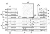
도 1 내지 도 3을 참조하면, 인쇄회로기판(100)은 제1 절연층(110), 제2 절연층(120), 제3 절연층(130), 회로패턴(141, 141, 143, 144, 145, 146, 147, 148), 비아(V1, V2, V3, V4, V5, V6, V7), 보호층(151, 152)을 포함한다.1 to 3, the printed
제1 절연층(110)은 인쇄회로기판(100)의 중앙에 배치된 절연층일 수 있다. The first insulating
제1 절연층(110)의 상부에는 제2 절연층(120)이 배치된다.A second insulating
또한, 제1 절연층(110)의 하부에는 제3 절연층(130)이 배치된다.In addition, a third
이때, 도면 상에는 제1 절연층(110)이 인쇄회로기판(100)의 전체 적층 구조에서, 정중앙층에 배치되는 것으로 도시하였으나, 이에 한정되지는 않는다. 즉, 상기 제1 절연층(110)은 인쇄회로기판(100)의 전체 적층 구조에서, 상부측에 치우친 위치에 배치될 수도 있으며, 이와 반대로 하부측에 치우친 위치에 배치될 수도 있을 것이다.In this case, in the drawings, the first insulating
제1 절연층(110)의 상부에는 제2 절연층(120)이 배치된다. 이때, 제2 절연층(120)은 복수의 층 구조를 가진다. 예를 들어, 제2 절연층(120)은 상기 제1 절연층(110)의 상면 위에 배치된 제2-1 절연층(121)과, 상기 제2-1 절연층(121)의 상면 위에 배치된 제2-2 절연층(122)과, 상기 제2-2 절연층(122)의 상면 위에 배치된 제2-3 절연층(123)을 포함할 수 있다. 이때, 도면 상에는 상기 제2 절연층(120)이 3층 구조를 가지는 것으로 도시하였으나, 이에 한정되지 않는다. 즉, 제2 절연층(120)은 2층 이하로 구성될 수도 있을 것이며, 이와 다르게 4층 이상의 구조를 가지며 구성될 수도 있을것이다.A second insulating
또한, 제1 절연층(110)의 하부에는 제3 절연층(130)이 배치된다. 이때, 제3 절연층(130)은 복수의 층 구조를 가진다. 예를 들어, 제3 절연층(130)은 상기 제1 절연층(110)의 하면 아래에 배치된 제3-1 절연층(131)과, 상기 제3-1 절연층(131)의 하면 아래에 배치된 제3-2 절연층(132)과, 상기 제3-2 절연층(132)의 하면 아래에 배치된 제3-3 절연층(133)을 포함할 수 있다. 이때, 도면 상에는 상기 제3 절연층(130)이 3층 구조를 가지는 것으로 도시하였으나, 이에 한정되지 않는다. 즉, 제2 절연층(130)은 2층 이하로 구성될 수도 있을 것이며, 이와 다르게 4층 이상의 구조를 가지며 구성될 수도 있을것이다.In addition, a third
또한, 도면 상에는 인쇄회로기판(100)이 절연층을 기준으로 7층 구조를 가지는 것으로 도시하였으나, 이에 한정되지 않는다. 예를 들어, 인쇄회로기판(100)은 절연층을 기준으로 6층 이하의 층수를 가질 수도 있으며, 이와 다르게 8층 이상의 층수를 가질 수도 있을 것이다.Further, in the drawings, the printed
제1 절연층(110), 제2 절연층(120) 및 제3 절연층(130)은 배선을 변경할 수 있는 전기 회로가 편성되어 있는 기판으로, 표면에 회로패턴들을 형성할 수 있는 절연 재료로 만들어진 프린트, 배선판 및 절연기판을 모두 포함할 수 있다. The first insulating
예를 들어, 제1 절연층(110), 제2 절연층(120) 및 제3 절연층(130) 중 적어도 하나는 리지드(rigid)하거나 또는 플렉서블(flexible)할 수 있다. 예를 들어, 상기 제1 절연층(110), 제2 절연층(120) 및 제3 절연층(130) 중 적어도 하나는 유리 또는 플라스틱을 포함할 수 있다. 자세하게, 상기 제1 절연층(110), 제2 절연층(120) 및 제3 절연층(130) 중 적어도 하나는, 소다라임유리(soda lime glass) 또는 알루미노실리케이트유리 등의 화학 강화/반강화유리를 포함하거나, 폴리이미드(Polyimide, PI), 폴리에틸렌 테레프탈레이트(polyethylene terephthalate, PET), 프로필렌 글리콜(propylene glycol, PPG) 폴리 카보네이트(PC) 등의 강화 혹은 연성 플라스틱을 포함하거나 사파이어를 포함할 수 있다.For example, at least one of the first insulating
또한, 상기 제1 절연층(110), 제2 절연층(120) 및 제3 절연층(130) 중 적어도 하나는 광등방성 필름을 포함할 수 있다. 일례로, 상기 제1 절연층(110), 제2 절연층(120) 및 제3 절연층(130) 중 적어도 하나는 COC(Cyclic Olefin Copolymer), COP(Cyclic Olefin Polymer), 광등방 폴리카보네이트(polycarbonate, PC) 또는 광등방 폴리메틸메타크릴레이트(PMMA) 등을 포함할 수 있다.In addition, at least one of the first insulating
또한, 상기 제1 절연층(110), 제2 절연층(120) 및 제3 절연층(130) 중 적어도 하나는 부분적으로 곡면을 가지면서 휘어질 수 있다. 즉, 제1 절연층(110), 제2 절연층(120) 및 제3 절연층(130) 중 적어도 하나는 부분적으로는 평면을 가지고, 부분적으로는 곡면을 가지면서 휘어질 수 있다. 자세하게, 상기 제1 절연층(110), 제2 절연층(120) 및 제3 절연층(130) 중 적어도 하나는 끝단이 곡면을 가지면서 휘어지거나 랜덤한 곡률을 포함한 표면을 가지며 휘어지거나 구부러질 수 있다.In addition, at least one of the first insulating
또한, 상기 제1 절연층(110), 제2 절연층(120) 및 제3 절연층(130) 중 적어도 하나는 유연한 특성을 가지는 플렉서블(flexible) 기판일 수 있다. 또한, 상기 제1 절연층(110), 제2 절연층(120) 및 제3 절연층(130) 중 적어도 하나는 커브드(curved) 또는 벤디드(bended) 기판일 수 있다. 이때, 제1 절연층(110), 제2 절연층(120) 및 제3 절연층(130) 중 적어도 하나는 회로 설계를 근거로 회로부품을 접속하는 전기배선을 배선 도형으로 표현하며, 절연물 상에 전기도체를 재현할 수 있다. 또한 제1 절연층(110), 제2 절연층(120) 및 제3 절연층(130) 중 적어도 하나는 전기 부품을 탑재하고 이들을 회로적으로 연결하는 배선을 형성할 수 있으며, 부품의 전기적 연결기능 외의 부품들을 기계적으로 고정시켜줄 수 있다.In addition, at least one of the first insulating
상기 제1 절연층(110), 제2 절연층(120) 및 제3 절연층(130)으 표면에는 회로 패턴들이 배치될 수 있다.Circuit patterns may be disposed on surfaces of the first insulating
예를 들어, 제1 절연층(110)의 상면에는 제1 회로 패턴(141)이 배치될 수 있다. 이때, 제1 회로 패턴(141)은 상호 일정 간격 이격되면서, 상기 제1 절연층(110)의 상면에 복수 개 배치될 수 있다.For example, a
제1 절연층(110)의 하면에는 제2 회로 패턴(142)이 배치될 수 있다. 제2 회로 패턴(142)은 상호 일정 간격 이격되면서, 상기 제1 절연층(110)의 하면에 복수 개 배치될 수 있다.A
또한, 제2 절연층(120)의 표면에도 회로패턴들이 배치될 수 있다. 예를 들어, 제2-1 절연층(121)의 상면에는 상호 일정 간격 이격되며 복수의 제3 회로 패턴(143)이 배치될 수 있다. 또한, 제2-2 절연층(122)의 상면에는 상호 일정 간격 이격되며 복수의 제4 회로 패턴(144)이 배치될 수 있다. 또한, 제2-3 절연층(123)의 상면에는 상호 일정 간격 이격되며 복수의 제5 회로 패턴(145)이 배치될 수 있다.Also, circuit patterns may be disposed on the surface of the second insulating
또한, 제3 절연층(130)의 표면에도 회로 패턴들이 배치될 수 있다. 예를 들어, 제3-1 절연층(131)의 하면에는 상호 일정 간격 이격되며 복수의 제6 회로 패턴(146)이 배치될 수 있다. 또한, 제3-2 절연층(132)의 하면에는 상호 일정 간격 이격되며 복수의 제7 회로 패턴(147)이 배치될 수 있다. 또한, 제3-3 절연층(133)의 하면에는 상호 일정 간격 이격되며 복수의 제8 회로 패턴(148)이 배치될 수 있다.Also, circuit patterns may be disposed on the surface of the third insulating
한편, 상기와 같은 제1 내지 제8 회로 패턴(141, 142, 143, 144, 145, 146, 147, 148)은 전기적 신호를 전달하는 배선으로, 전기 전도성이 높은 금속물질로 형성될 수 있다. 이를 위해, 상기 제1 내지 제8 회로 패턴(141, 142, 143, 144, 145, 146, 147, 148)은 금(Au), 은(Ag), 백금(Pt), 티타늄(Ti), 주석(Sn), 구리(Cu) 및 아연(Zn) 중에서 선택되는 적어도 하나의 금속 물질로 형성될 수 있다. 또한 상기 제1 내지 제8 회로 패턴(141, 142, 143, 144, 145, 146, 147, 148)은 본딩력이 우수한 금(Au), 은(Ag), 백금(Pt), 티타늄(Ti), 주석(Sn), 구리(Cu), 아연(Zn) 중에서 선택되는 적어도 하나의 금속 물질을 포함하는 페이스트 또는 솔더 페이스트로 형성될 수 있다. 바람직하게, 상기 제1 내지 제8 회로 패턴(141, 142, 143, 144, 145, 146, 147, 148)은 전기전도성이 높으면서 가격이 비교적 저렴한 구리(Cu)로 형성될 수 있다. Meanwhile, the first to
상기 제1 내지 제8 회로 패턴(141, 142, 143, 144, 145, 146, 147, 148)은 통상적인 인쇄회로기판의 제조 공정인 어디티브 공법(Additive process), 서브트렉티브 공법(Subtractive Process), MSAP(Modified Semi Additive Process) 및 SAP(Semi Additive Process) 공법 등으로 가능하며 여기에서는 상세한 설명은 생략한다. The first to eighth circuit patterns (141, 142, 143, 144, 145, 146, 147, 148) are an additive process and a subtractive process, which are conventional printed circuit board manufacturing processes. ), MSAP (Modified Semi Additive Process) and SAP (Semi Additive Process) methods, etc., and detailed descriptions are omitted here.
한편, 제1 회로 패턴(141)은 상기 제1 절연층(110)의 상면에 배치되면서, 캐비티(160)를 통해 노출되는 패드(141a)를 포함할 수 있다. 상기 패드(141a)는 상기 캐비티(160) 내에 실장되는 전자 소자(추후 설명)와 전기적으로 연결될 수 있다. 예를 들어, 패드(141a)는 상기 캐비티(160) 내에 실장되는 전자 소자와 와이어를 통해 연결되는 와이어 본딩 패드일 수 있다. 이와 다르게, 패드(141a)는 상기 캐비티(160) 내에 실장되는 전자 소자의 단자와 직접 연결되는 플립칩 본딩 패드일 수 있다. 이에 대해서는 하기에서 더욱 상세히 설명하기로 한다.Meanwhile, the
한편, 제1 내지 제8 회로 패턴(141, 142, 143, 144, 145, 146, 147, 148)은 각각 층간 도통을 위한 비아와 연결되는 패턴과, 신호 전달을 위한 패턴과, 전자 소자 등과 연결되는 패드를 포함할 수 있다.Meanwhile, the first to
제1 절연층(110), 제2 절연층(120) 및 제3 절연층(130)에는 서로 다른 층에 배치된 회로패턴들을 상호 전기적으로 연결하는 비아(V1, V2, V3, V4, V5, V6, V7)가 배치될수 있다. 비아(V1, V2, V3, V4, V5, V6, V7)는 상기 제1 절연층(110), 제2 절연층(120) 및 제3 절연층(130) 중 적어도 어느 하나를 관통하며 배치될 수 있다. 그리고, 비아(V1, V2, V3, V4, V5, V6, V7)의 양단은 서로 다른 절연층에 배치된 회로패턴들과 각각 연결되며, 그에 따라 전기적 신호를 전달할 수 있다.Vias V1, V2, V3, V4, V5, which electrically connect circuit patterns disposed on different layers to each other, in the first insulating
제1 절연층(110)에는 제1 비아(V1)가 배치될 수 있다. 제1 비아(V1)는 상기 제1 절연층(110)의 상면 및 하면을 관통하며 배치될 수 있다. 제1 비아(V1)는 제1 절연층(110)의 상면에 배치된 제1 회로 패턴(141)과 상기 제1 절연층(110)의 하면에 배치된 제2 회로 패턴(142)을 전기적으로 연결할 수 있다.A first via V1 may be disposed in the first insulating
제2 절연층(120)에는 복수의 비아가 배치될 수 있다. 즉, 제2-1 절연층(121)에는 제2 비아(V2)가 배치될 수 있다. 제2 비아(V2)는 제1 절연층(110)의 상면에 배치된 제1 회로 패턴(141)과, 상기 제2-1 절연층(121)의 상면에 배치된 제3 회로 패턴(143)을 전기적으로 연결할 수 있다.A plurality of vias may be disposed in the second insulating
또한, 제2-2 절연층(122)에는 제3 비아(V3)가 배치될 수 있다. 제3 비아(V3)는 상기 제2-2 절연층(122)의 상면에 배치된 제4 회로 패턴(144)과 상기 제2-1 절연층(121)의 상면에 배치된 제3 회로 패턴(143)을 전기적으로 연결할 수 있다.In addition, a third via V3 may be disposed in the 2-2
또한, 제2-3 절연층(123)에는 제4 비아(V4)가 배치될 수 있다. 제4 비아(V4)는 상기 제2-3 절연층(123)의 상면에 배치된 제5 회로 패턴(145)과 상기 제2-2 절연층(122)의 상면에 배치된 제4 회로 패턴(144)을 전기적으로 연결할 수 있다.Also, a fourth via V4 may be disposed in the 2-3rd
제3 절연층(130)에는 복수의 비아가 배치될 수 있다. 즉, 제3-1 절연층(131)에는 제5 비아(V5)가 배치될 수 있다. 제5 비아(V5)는 제1 절연층(110)의 하면에 배치된 제2 회로 패턴(142)과, 상기 제3-1 절연층(131)의 하면에 배치된 제6 회로 패턴(146)을 전기적으로 연결할 수 있다.A plurality of vias may be disposed in the third insulating
또한, 제3-2 절연층(132)에는 제6 비아(V6)가 배치될 수 있다. 제6 비아(V6)는 상기 제3-2 절연층(132)의 하면에 배치된 제7 회로 패턴(147)과 상기 제3-1 절연층(131)의 하면에 배치된 제6 회로 패턴(146)을 전기적으로 연결할 수 있다.In addition, a sixth via V6 may be disposed in the 3-2th
또한, 제3-3 절연층(133)에는 제7 비아(V7)가 배치될 수 있다. 제7 비아(V7)는 상기 제3-3 절연층(133)의 하면에 배치된 제8 회로 패턴(148)과 상기 제3-2 절연층(132)의 하면에 배치된 제7 회로 패턴(147)을 전기적으로 연결할 수 있다.In addition, a seventh via V7 may be disposed in the 3-3
한편, 상기 비아(V1, V2, V3, V4, V5, V6, V7)는 상기 제1 절연층(110), 제2 절연층(120) 및 제3 절연층(130) 중 어느 하나의 절연층만을 관통할 수 있으며, 이와 다르게 복수의 절연층을 공통으로 관통하며 배치될 수도 있다. 이에 따라, 비아(V1, V2, V3, V4, V5, V6, V7)는 서로 이웃하는 절연층이 아닌 적어도 2층 이상 떨어진 절연층의 표면 상에 배치된 회로패턴들을 서로 연결할 수도 있을 것이다.On the other hand, the vias V1, V2, V3, V4, V5, V6, V7 are only one of the first insulating
한편, 상기 비아(V1, V2, V3, V4, V5, V6, V7)는 상기 복수의 절연층 중 적어도 하나의 절연층을 관통하는 관통 홀(도시하지 않음) 내부를 전도성 물질로 충진하여 형성할 수 있다.Meanwhile, the vias V1, V2, V3, V4, V5, V6, and V7 are formed by filling the inside of a through hole (not shown) penetrating at least one of the plurality of insulating layers with a conductive material. I can.
상기 관통 홀은 기계, 레이저 및 화학 가공 중 어느 하나의 가공 방식에 의해 형성될 수 있다. 상기 관통 홀이 기계 가공에 의해 형성되는 경우에는 밀링(Milling), 드릴(Drill) 및 라우팅(Routing) 등의 방식을 사용할 수 있고, 레이저 가공에 의해 형성되는 경우에는 UV나 Co2 레이저 방식을 사용할 수 있으며, 화학 가공에 의해 형성되는 경우에는 아미노실란, 케톤류 등을 포함하는 약품을 이용하여 상기 복수의 절연층 중 적어도 하나의 절연층을 개방할 수 있다.The through hole may be formed by any one of mechanical, laser, and chemical processing. When the through hole is formed by machining, methods such as milling, drilling, and routing can be used, and when formed by laser processing, UV or Co 2 laser method is used. In the case of forming by chemical processing, at least one of the plurality of insulating layers may be opened using a chemical containing aminosilane, ketones, or the like.
한편, 상기 레이저에 의한 가공은 광학 에너지를 표면에 집중시켜 재료의 일부를 녹이고 증발시켜, 원하는 형태를 취하는 절단 방법으로, 컴퓨터 프로그램에 의한 복잡한 형성도 쉽게 가공할 수 있고, 다른 방법으로는 절단하기 어려운 복합 재료도 가공할 수 있다. On the other hand, the laser processing is a cutting method that takes a desired shape by concentrating optical energy on the surface to melt and evaporate a part of the material, and it is possible to easily process complex formations by a computer program. Even difficult composite materials can be processed.
또한, 상기 레이저에 의한 가공은 절단 직경이 최소 0.005mm까지 가능하며, 가공 가능한 두께 범위로 넓은 장점이 있다.In addition, the laser processing has a cutting diameter of at least 0.005mm, and has a wide range of possible thicknesses.
상기 레이저 가공 드릴로, YAG(Yttrium Aluminum Garnet)레이저나 Co2 레이저나 자외선(UV) 레이저를 이용하는 것이 바람직하다. YAG 레이저는 동박층 및 절연층 모두를 가공할 수 있는 레이저이고, Co2 레이저는 절연층만 가공할 수 있는 레이저이다.As the laser processing drill, it is preferable to use a YAG (Yttrium Aluminum Garnet) laser, a Co 2 laser, or an ultraviolet (UV) laser. YAG laser is a laser capable of processing both copper foil layers and insulating layers, and Co 2 laser is a laser capable of processing only insulating layers.
상기 관통 홀이 형성되면, 상기 관통 홀 내부를 전도성 물질로 충진하여 상기 비아(V1, V2, V3, V4, V5, V6, V7)를 형성할 수 있다. 상기 비아(V1, V2, V3, V4, V5, V6, V7)를 형성하는 금속 물질은 구리(Cu), 은(Ag), 주석(Sn), 금(Au), 니켈(Ni) 및 팔라듐(Pd) 중에서 선택되는 어느 하나의 물질일 수 있으며, 상기 전도성 물질 충진은 무전해 도금, 전해 도금, 스크린 인쇄(Screen Printing), 스퍼터링(Sputtering), 증발법(Evaporation), 잉크젯팅 및 디스펜싱 중 어느 하나 또는 이들의 조합된 방식을 이용할 수 있다.When the through hole is formed, the vias V1, V2, V3, V4, V5, V6, and V7 may be formed by filling the inside of the through hole with a conductive material. Metal materials forming the vias (V1, V2, V3, V4, V5, V6, V7) are copper (Cu), silver (Ag), tin (Sn), gold (Au), nickel (Ni), and palladium ( Pd) may be any one material selected from, and the conductive material filling may be any of electroless plating, electroplating, screen printing, sputtering, evaporation, ink jetting, and dispensing. One or a combination thereof may be used.
한편, 제1 절연층(110), 제2 절연층(120) 및 제3 절연층(130) 중 최외곽에 배치된 절연층의 표면에는 보호층(151, 152)이 배치될 수 있다. 예를 들어, 복수의 절연층 중 최상부에 배치된 절연층의 상면에는 제1 보호층(151)이 배치될 수 있다. 예를 들어, 제2 절연층(120) 중 최상부에 배치된 제2-3 절연층(123)의 상면에는 제1 보호층(151)이 배치될 수 있다. 또한, 복수의 절연층 중 최하부에 배치된 절연층의 하면에는 제2 보호층(152)이 배치될 수 있다. 예를 들어, 제3 절연층(130) 중 최하부에 배치된 제3-3 절연층(133)의 하면에는 제2 보호층(152)이 배치될 수 있다.Meanwhile, the
상기 제1 보호층(151) 및 제2 보호층(152)은 각각 개구부를 가질 수 있다. 예를들어, 제1 보호층(151)은 제2-3 절연층(123)의 상면에 배치된 제5 회로 패턴(145) 중 노출되어야 하는 제5 회로 패턴의 표면을 노출하는 개구부를 가질 수 있다. Each of the first and second
또한, 제2 보호층(152)은 제3-3 절연층(133)의 하면에 배치된 제8 회로 패턴(148) 중 노출되어야 하는 제8 회로 패턴의 표면을 노출하는 개구부를 가질 수 있다.In addition, the
이러한 제1 보호층(151) 및 제2 보호층(152)은 절연성 물질을 포함할 수 있다. 제1 보호층(151) 및 제2 보호층(152)은 회로패턴들의 표면을 보호하기 위해 도포된 후 가열하여 경화될 수 있는 다양한 물질을 포함할 수 있다. 상기 제1 보호층(151) 및 제2 보호층(152)은 레지스트(resist)층일 수 있다. 예를 들어, 제1 보호층(151) 및 제2 보호층(152)은 유기고분자 물질을 포함하는 솔더 레지스트층일 수 있다. 일예로, 상기 제1 보호층(151) 및 제2 보호층(152)은 에폭시 아크릴레이트 계열의 수지를 포함할 수 있다. 자세하게, 제1 보호층(151) 및 제2 보호층(152)은 수지, 경화제, 광개시제, 안료, 용매, 필러, 첨가제, 아크릴 계열의 모노머 등을 포함할 수 있다. 다만, 실시 예는 이에 한정되지 않고, 상기 제1 보호층(151) 및 제2 보호층(152)은 포토솔더 레지스트층, 커버레이(cover-lay) 및 고분자 물질 중 어느 하나일 수 있음은 물론이다.The
상기 제1 보호층(151) 및 제2 보호층(152)의 두께는 1㎛ 내지 20㎛일 수 있다. 상기 제1 보호층(151) 및 제2 보호층(152)의 두께는 1㎛ 내지 15㎛일 수 있다. 예를 들어, 상기 제1 보호층(151) 및 제2 보호층(152)의 두께는 5㎛ 내지 20㎛일 수 있다. 상기 제1 보호층(151) 및 제2 보호층(152)의 두께가 20㎛ 초과인 경우에는 인쇄회로기판(100)의 두께가 증가할 수 있다. 상기 제1 보호층(151) 및 제2 보호층(152)의 두께가 1㎛ 미만인 경우에는 인쇄회로기판(100)에 포함된 회로 패턴들의 신뢰성이 저하될 수 있다. The first and second
한편, 제2 절연층(120)에는 캐비티(160)가 형성될 수 있다. 이때, 상기 캐비티(160)는 복수의 층으로 구성되는 제2 절연층(120) 내에 배치될 수 있다. 이때, 캐비티(160)는 상기 복수의 층으로 구성된 제2 절연층(120) 중 적어도 하나의 절연층을 관통하며 배치되고, 적어도 다른 하나의 절연층을 비관통하며 배치될 수 있다.Meanwhile, a
즉, 일반적인 캐비티(160)는 절연층을 관통하며 배치된다. 이에 따라, 캐비티(160)가 배치될 위치에서, 상기 캐비티(160)와 수평 방향으로 중첩되는 절연층은 존재하지 않게 된다. 예를 들어, 비교 예에서의 캐비티는 상기 제2 절연층(120)의 전체를 관통하며 배치된다. 예를 들어, 비교 예에서의 캐비티는 제2-1 절연층(121)의 하면 및 제2-3 절연층(123)의 상면을 관통하며 배치된다. That is, the
이와 다르게, 실시 예에서의 캐비티는 캐비티가 배치될 위치에서, 상기 캐비티(160)와 수직으로 중첩되는 절연층 중 적어도 하나의 절연층은 관통하면서, 적어도 다른 하나의 절연층은 관통하지 않는다.In contrast, the cavity in the embodiment penetrates at least one of the insulating layers vertically overlapping with the
즉, 실시 예에서의 캐비티(160)는 상기 제2 절연층(120)에 배치된다. 즉, 캐비티(160)는 제2-1 절연층(121), 제2-2 절연층(122) 및 제2-3 절연층(123) 내에 배치된다. That is, the
이때, 비교 예의 인쇄회로기판의 구조에서의 캐비티는 상기 제2-1 절연층(121), 제2-2 절연층(122) 및 제2-3 절연층(123)을 모두 관통하며 배치된다. 이에 따라, 비교 예의 인쇄회로기판에는 캐비티와 수직으로 중첩되는 영역에서의 제1 절연층의 상면은 노출된다. 즉, 비교 예의 인쇄회로기판에서의 상기 캐비티와 수직으로 중첩되는 제1 절연층의 상면에는 제2 절연층(보다 명확하게는, 제2-1 절연층)이 존재하지 않는다.In this case, the cavity in the structure of the printed circuit board of the comparative example is disposed to penetrate through all of the 2-1
이에 반하여, 실시 예에서의 인쇄회로기판(100)에서의 캐비티(160)는 제2-1 절연층(121) 및 제2-2 절연층(122)을 관통하면서, 상기 제2-3 절연층(123)을 비관통하며 배치될 수 있다. On the other hand, the
즉, 캐비티(160)는 제2-1 절연층(121) 내에 배치되는 제1 파트(P1)와, 제2-2 절연층(122) 내에 배치되는 제2 파트(P2)와, 제2-3 절연층(123) 내에 배치되는 제3 파트(P3)를 포함할 수 있다. 여기에서, 실시 예에서의 제2 절연층(122)이 3층 구조를 가짐에 따라 상기 캐비티(160)가 제1 내지 제3파트(P1, P2, P3)로 구성되는 것으로 도시하였으나, 이에 한정되지는 않는다. 예를 들어, 제2 절연층(120)이 2층 구조를 가지는 경우, 상기 캐비티(160)는 제1 및 제2 파트만을 포함할 수 있다. 예를 들어, 상기 제2 절연층(122)이 5층 구조를 가지는 경우, 상기 캐비티(160)는 제1 내지 제5 파트를 포함할 수 있다. 다만, 실시 예에서의 캐비티(160)는 최하부에 배치된 파트가 관통홀 형상이 아닌 홈 형상을 가진다는 것에 그 특징이 있다.That is, the
상기 제1 파트(P1)는, 상기 제2-1 절연층(121) 내에 배치될 수 있다. 이때, 제1 파트(P1)는, 상기 제2-1 절연층(121) 내에 배치되며, 상기 캐비티(160)의 하부 영역을 형성하는 홈(Groove)일 수 있다.The first part P1 may be disposed in the 2-1
상기 제2 파트(P2)는 상기 제2-2 절연층(122) 내에 배치될 수 있다. 상기 제2 파트(P2)는 상기 제2-2 절연층(122) 내에 배치되며, 상기 캐비티(160)의 중앙 영역을 형성하는 관통 홀일 수 있다. The second part P2 may be disposed in the 2-2
상기 제3 파트(P3)는 상기 제2-3 절연층(123) 내에 배치될 수 있다. 상기 제3 파트(P3)는 상기 제2-3 절연층(123) 내에 배치되며, 상기 캐비티(160)의 상부 영역을 형성하는 관통 홀일 수 있다. The third part P3 may be disposed in the 2-3rd
즉, 캐비티(160)는 상기 제1 파트(P1), 제2 파트(P2) 및 제3 파트(P3)의 조합으로 구성될 수 있다. 이때, 상기 제1 파트(P1)의 두께는 상기 제2-1 절연층(121)의 두께보다 작을 수 있다. 따라서, 상기 캐비티(160)는 상기 제2-1 절연층(121)을 비관통하며 형성될 수 있다. That is, the
다시 말해서, 제2-1 절연층(121)은 상기 캐비티(160)와 수직 방향으로 오버랩되는 영역 상에 배치되는 제1 영역(R1)과, 상기 제1 영역(R1)을 제외한 제2 영역(R2)을 포함할 수 있다. 그리고, 상기 제1 영역(R1)의 두께는 상기 제2 영역(R2)의 두께와 다를 수 있다.In other words, the 2-1
바람직하게, 상기 제2 영역(R2)의 두께(H1)는 상기 제2-1 절연층(121)이 가지는 두께일 수 있다. Preferably, the thickness H1 of the second region R2 may be the thickness of the 2-1
상기 제2 영역(R2)의 두께(H1)는 20㎛ 내지 100㎛일 수 있다. 예를 들어, 상기 제2 영역(R2)의 두께(H1)는 25㎛ 내지 50㎛의 두께를 가질 수 있다. 예를 들어, 상기 제2 영역(R2)의 두께(H1)는 30㎛ 내지 40㎛의 두께를 가질 수 있다. 상기 제2 영역(R2)의 두께(H1)가 100㎛를 초과하는 경우에는 전체적인 인쇄회로기판(100)의 두께가 증가할 수 있다. 상기 제2 영역(R2)의 두께(H1)가 상기 20㎛ 미만인 경우에는 패드(141a)나, 제1 회로 패턴을 안정적으로 보호할 수 없다. 또한, 상기 제2 영역(R2)의 두께(H1)가 상기 20㎛ 미만인 경우에는, 전자 소자를 실장하는 공정에서 상기 제2-1 절연층(121)이 열/압력 등에 취약할 수 있다.The thickness H1 of the second region R2 may be 20 μm to 100 μm. For example, the thickness H1 of the second region R2 may have a thickness of 25 μm to 50 μm. For example, the thickness H1 of the second region R2 may have a thickness of 30 μm to 40 μm. When the thickness H1 of the second region R2 exceeds 100 μm, the overall thickness of the printed
상기 제1 영역(R1)의 두께(H2)는 상기 제2 영역의 두께(H1)보다 작을 수 있다. 상기 제1 영역(R1)의 두께(H2)는 상기 패드(141a)의 두께(H3)에 의해 결정될 수 있다. 바람직하게, 상기 제1 영역(R1)의 두께(H2)는 상기 패드(141a)의 두께(H3)보다 작을 수 있다. The thickness H2 of the first region R1 may be smaller than the thickness H1 of the second region. The thickness H2 of the first region R1 may be determined by the thickness H3 of the
바람직하게, 상기 패드(141a)의 두께(H3)는 상기 제2 영역(R2)의 두께(H1)보다 작을 수 있다. 예를 들어, 상기 패드(141a)의 두께(H3)는 5㎛ 내지 30㎛일 수 있다.Preferably, the thickness H3 of the
그리고, 상기 제1 영역(R1)의 두께(H2)는 상기 패드(141a)의 두께(H3)보다 작을 수 있다. 예를들어, 제1 영(R1)역의 두께(H2)는 3㎛ 내지 25㎛일 수 있다. 따라서, 상기 제2-1 절연층(121)의 상기 제1 영역(R1)은 상기 제1 절연층(110) 상에 배치된다. 이때, 제2-1 절연층(121)의 상기 제1 영역(R1)은 상기 제1 절연층(110) 상에 배치되는 패드(141a)의 상면을 노출할 수 있다. In addition, the thickness H2 of the first region R1 may be smaller than the thickness H3 of the
즉, 실시 예에서는 전자 소자를 실장시키기 위해, 상기 제2 절연층(120)을 관통하며 캐비티(160)를 형성하지 않고, 상기 제2 절연층(120)의 적어도 일부(상기 제2-1 절연층(121)의 제1 영역)를 상기 제1 절연층(110) 상에 잔존시킨 상태로 캐비티(160)를 형성한다.That is, in the embodiment, in order to mount an electronic device, at least a part of the second insulating
이때, 상기 잔존한 상기 제2 절연층(120)의 일부의 두께(H2)는 상기 캐비티(160) 상에서 노출되어야 하는 패드(141a)의 두께(H3)보다 작다. 이에 따라, 실시 예에서는 상기 패드(141a) 상에 전자 소자를 실장하는데 영향을 주지 않고 상기 패드(141a)의 형상을 유지시키면서 상기 캐비티(160)를 형성할 수 있다.In this case, the thickness H2 of a portion of the remaining second insulating
즉, 종래에는 상기와 같은 복수의 절연층 내에 캐비티를 형성하기 위해서, 보호 레이어나 스탑 레이어를 제1 절연층 상에 배치한 상태에서 캐비티 형성 공정을 진행하였다. 이에 따라, 종래에는 원하는 깊이(제2 절연층을 모두 관통하는 깊이)만큼 캐비티를 형성할 수 있었다. 다만, 종래에는 상기 캐비티가 형성된 이후에 상기 보호 레이어나 스탑 레이어를 제거하는 에칭 공정을 진행해야만 했다. 이에 따라, 종래에는 상기 보호 레이어나 스탑 레이어를 제거하는 에칭 공정 중에 상기 제1 절연층 상에 배치되는 패드의 일부도 함께 제거되며, 이에 따라 상기 패드의 신뢰성에 문제가 발생할 수 있다. 이때, 샌드블러스트(sand blast)나 레이저 공정 시에 필요한 보호 레이어나 스탑 레이어의 두께는 3um 내지 10um 수준이며, 이에 따라 상기 에칭 공정 시 상기 패드의 전체 두께 중 상기 보호 레이어나 스탑 레이어의 두께에 대응하는 만큼 제거되는 문제가 있었다.That is, conventionally, in order to form cavities in the plurality of insulating layers as described above, a cavity forming process was performed while a protective layer or a stop layer is disposed on the first insulating layer. Accordingly, in the related art, a cavity could be formed to a desired depth (the depth which penetrates all the second insulating layers). However, in the related art, after the cavity is formed, an etching process for removing the protective layer or the stop layer has to be performed. Accordingly, in the related art, a part of the pad disposed on the first insulating layer is also removed during the etching process of removing the protective layer or the stop layer, which may cause a problem in reliability of the pad. At this time, the thickness of the protective layer or the stop layer required for the sand blast or laser process is 3 um to 10 um, and accordingly, the thickness of the protective layer or the stop layer among the total thickness of the pad during the etching process There was a problem that was eliminated as much as it responded.
이에 따라, 실시 예에서는 상기 보호 레이어나 스탑 레이어를 형성시키지 않은 상태에서 캐비티를 용이하게 형성할 수 있도록 하며, 이에 따라 상기 보호 레이어나 스탑 레이어의 제거 공정 중에 발생하는 신뢰성 문제를 해결하도록 한다.Accordingly, in the embodiment, the cavity can be easily formed without the protection layer or the stop layer being formed, thereby solving the reliability problem that occurs during the removal process of the protection layer or the stop layer.
그리고 이는 상기 캐비티를 형성하는 공정 조건의 컨트롤을 통해 상기 제2-1 절연층(121)을 관통하지 않는 상태로 상기 캐비티(160)를 형성하도록 한다.In addition, this allows the
이때, 상기 캐비티(160)는 샌드블러스트 공정에 의해 형성될 수 있다. 샌드블러스트 공정에 의해 형성될 수 있다. 샌드블러스트 공정은 모래와 같은 연마제를 고압의 공기와 함께 노즐로부터 분사하여 기판 등의 표면에 충돌시켜 상기 기판 상에 원하는 형상의 관통 홀이나 캐비티를 형성하는 공정을 의미한다. 또한, 상기 캐비티(160)는 샌드블러스트 공정이 아닌 레이저 공정에 의해 형성될 수 있으며, 레이저 공정에 의한 형성 시에도 레이어 공정 조건의 컨트롤을 통해 상기 캐비티(160)를 원하는 깊이만큼 형성할 수 있다. 이하에서는, 상기 캐비티(160)가 샌드블러스트에 의해 형성되는 것으로 하여 설명하기로 하나, 실시 예는 이에 한정되지 않는다.In this case, the
여기에서, 상기 보호 레이어나 스탑 레이어가 없는 상태에서, 상기 샌드블러스트 공정을 통해 원하는 깊이까지 캐비티를 형성하는게 쉽지 않다. 이때, 실시 예에서는 상기 캐비티(160)가 가져야 하는 최소 깊이 및 최대 깊이 사이의 범위를 기준으로 상기 샌드블러스트의 공정 조건을 컨트롤 하여 원하는 깊이까지 상기 캐비티(160)를 형성할 수 있도록 한다. 여기에서 상기 컨트롤되는 공정 조건은 샌드 블러스트 공정 속도 및 압력을 포함할 수 있다. 즉, 상기 샌드블러스트 공정 진행 시간을 고정한 상태에서 상기 공정 속도 및 압력 조건을 변경함에 따라 상기 캐비티(160)의 깊이를 um 단위로 컨트롤 가능하다. 이에 따라, 실시 예에서는 상기 샌드블러스트 공정 속도 및 압력을 조정하여 상기 캐비티가 가져야 하는 최소 깊이 및 최대 깊이 사이의 범위 내에서 상기 캐비티(160)를 형성할 수 있도록 한다. 상기 캐비티(160)의 최대 깊이는 상기 제2 절연층(120)의 전체 두께보다 작을 수 있다. 또한, 상기 캐비티(160)의 최소 깊이는 상기 제2 절연층(120)의 전체 두께에서 상기 패드(141a)의 두께를 뺀 깊이보다 클 수 있다. 이에 따라, 실시 예에서는 상기 제2 절연층(120) 중 제2-1 절연층(121)의 제1 영역(R1)의 상면이 상기 제1 절연층(110)의 상면보다 높으면서 상기 패드(141a)의 상면보다는 낮게 위치하도록 한다.Here, in the absence of the protective layer or the stop layer, it is not easy to form a cavity to a desired depth through the sandblasting process. In this case, in the embodiment, the
한편, 도 2 및 도 3을 참조하면, 상기 캐비티(160)는 내벽(S1) 및 바닥면(S2)을 포함한다. Meanwhile, referring to FIGS. 2 and 3, the
상기 캐비티(160)의 내벽(S1) 및 바닥면(S2)은 일정 표면 거칠기를 가질 수 있다. 이때, 실시 예에서는 상기 캐비티(160)의 내벽(S1) 및 바닥면(S2)이 일정 표면 거칠기를 가지도록 추가적인 공정을 진행하는 것이 아니라, 상기 캐비티(160)를 형성하기 위한 샌드블러스트 공정 시에 상기 표면 거칠기가 형성되도록 할 수 있다. The inner wall S1 and the bottom surface S2 of the
다시 말해서, 상기 캐비티(160)의 바닥면(S2)은 상기 제2-1 절연층(121)의 제1 영역(R1)의 상면을 의미할 수 있다. 그리고, 상기 제2-1 절연층(121)의 제1 영역(R1)의 상면의 높이는 일정하지 않고, 위치에 따라 편차를 가질 수 있다. In other words, the bottom surface S2 of the
도 4은 제1 실시 예에 따른 패키지 기판을 나타낸 도면이다.4 is a diagram illustrating a package substrate according to the first embodiment.
도 4를 참조하면, 실시 예에서의 패키지 기판(200)은 도 1에 도시한 인쇄회로기판(100) 및 상기 인쇄회로기판(100)의 캐비티(160) 내에 실장된 전자소자(180)를 포함한다.Referring to FIG. 4, the
도 1에서 설명한 인쇄회로기판(100)은 전자소자(180)를 실장하기 위한 패키지 기판(200)으로 이용될 수 있다. The printed
이때, 상기 인쇄회로기판(100)에 대해서는 도1에서 이미 상세하게 설명하였으므로, 이에 대한 설명은 생략하기로 한다.In this case, since the printed
인쇄회로기판(100)은 캐비티(160)를 포함하고, 상기 캐비티(160)에는 패드(141a)가 노출될 수 있다. 이때, 상기 캐비티(160) 내에서 상기 패드(141a)가 형성된 영역을 제외한 나머지 영역에는 상기 제2-1 절연층(121)이 배치될 수 있다. 다만, 상기 제2-1 절연층(121)의 제1 영역(R1)의 높이는 상기 패드(141a)의 높이보다 낮다. 이에 따라 상기 전자소자(180)는 상기 제1 영역(R1) 상의 상기 제2-1 절연층(121)에 의해 영향을 받지 않고, 상기 패드(141a) 상에 안정적으로 실장될 수 있다. 다시 말해서, 상기 패드(141a)의 높이보다 상기 제2-1 절연층(121)의 상기 제1 영역(R1)의 높이가 높다면, 상기 전자소자(180)는 상기 패드(141a) 상에 기울어진 상태로 실장될 수 있으며, 더 나아가 상기 패드(141a)와 전기적 접속 상태에 불량이 발생할 수 있다. The printed
이때, 상기 전자소자(180)는 인쇄회로기판(100)의 캐비티(160) 내에 배치되는 전자 부품일 수 있으며, 이는 능동 소자와 수동 소자로 구분될 수 있다. 그리고, 상기 능동 소자는 비선형 부분을 적극적으로 이용한 소자이고, 수동 소자는 선형 및 비선형 특성이 모두 존재하여도 비선형 특성은 이용하지 않는 소자를 의미한다. 그리고, 상기 수동 소자에는 트랜지스터, IC 반도체 칩 등이 포함될 수 있으며, 상기 수동 소자에는 콘덴서, 저항 및 인덕터 등을 포함할 수 있다. 상기 수동 소자는 능동 소자인 반도체 칩의 신호 처리 속도를 높이거나, 필터링 기능 등을 수행하기 위해, 통상의 인쇄회로기판에 실장된다.In this case, the
한편, 상기 패드(141a) 상에는 접속부(170)가 배치될 수 있다. 상기 접속부(170)의 평면 형상은 사각형일 수 있다. 상기 접속부(170)는 상기 패드(141a) 상에 배치되어, 상기 전자소자(180)를 고정하면서 상기 전자소자(180)와 상기 패드(141a) 사이를 전기적으로 연결한다. 이를 위해, 패드(141a)는 전도성 물질로 형성될 수 있다. 일 예로 상기 접속부(170)는 솔더 볼일 수 있다. 상기 접속부(170)는 솔더에 이종 성분의 물질이 함유될 수 있다. 상기 솔더는 SnCu, SnPb, SnAgCu 중 적어도 어느 하나로 구성될 수 있다. 그리고, 상기 이종 성분의 물질은 Al, Sb, Bi, Cu, Ni, In, Pb, Ag, Sn, Zn, Ga, Cd 및 Fe 중 어느 하나를 포함할 수 있다.Meanwhile, a
한편, 상기 전자소자(180)의 상면은 상기 인쇄회로기판(100)의 최상층의 표면보다 높게 위치할 수 있다. 다만, 실시 예는 이에 한정되지 않으며, 상기 전자소자(180)의 종류에 따라 상기 전자소자(180)의 상면이 상기 인쇄회로기판(100)의 최상층의 표면과 동일 높이에 배치될 수 있으며, 이와 다르게 낮게 배치될 수도 있을 것이다.Meanwhile, an upper surface of the
도 5는 제2 실시 예에 따른 패키지 기판을 나타낸 도면이다.5 is a diagram illustrating a package substrate according to a second embodiment.
도 5를 참조하면, 실시 예에서의 패키지 기판(200A)은 도 1에 도시한 인쇄회로기판(100) 및 상기 인쇄회로기판(100)의 캐비티(160) 내에 실장된 전자소자(180a)를 포함한다.Referring to FIG. 5, the
또한, 패키지 기판(200A)은 상기 캐비티(160) 내에 배치되며, 상기 전자소자(180a)를 덮는 몰딩층(190)을 더 포함한다.In addition, the
상기 몰딩층(190)은 선택적으로 상기 캐비티(160) 내에 배치되어, 상기 캐비티(160) 내에 실장된 전자소자(180a)를 보호할 수 있다. The molding layer 190 may be selectively disposed in the
상기 몰딩층(190)은 몰딩용 수지로 구성될 수 있으며, 예를 들어, EMC(Epoxy molding compound)일 수 있다. 다만, 실시 예는 이에 한정되지 않으며, 상기 몰딩층(190)은 EMC 이외에도 다양한 다른 몰딩용 수지로 구성될 수도 있을 것이다.The molding layer 190 may be formed of a molding resin, and may be, for example, an epoxy molding compound (EMC). However, the embodiment is not limited thereto, and the molding layer 190 may be formed of various other molding resins in addition to EMC.
도 1에서 설명한 인쇄회로기판(100)은 전자소자(180a)를 실장하기 위한 패키지 기판(200A)으로 이용될 수 있다. The printed
인쇄회로기판(100)은 캐비티(160)를 포함하고, 상기 캐비티(160)에는 패드(141a)가 노출될 수 있다. 이때, 상기 캐비티(160) 내에서 상기 패드(141a)가 형성된 영역을 제외한 나머지 영역에는 상기 제2-1 절연층(121)이 배치될 수 있다. 다만, 상기 제2-1 절연층(121)의 제1 영역(R1)의 높이는 상기 패드(141a)의 높이보다 낮다. 이에 따라 상기 전자소자(180a)는 상기 제1 영역(R1) 상의 상기 제2-1 절연층(121)에 의해 영향을 받지 않고, 상기 패드(141a) 상에 안정적으로 실장될 수 있다. 다시 말해서, 상기 패드(141a)의 높이보다 상기 제2-1 절연층(121)의 상기 제1 영역(R1)의 높이가 높다면, 상기 전자소자(180a)는 상기 패드(141a) 상에 기울어진 상태로 실장될 수 있으며, 더 나아가 상기 패드(141a)와 전기적 접속 상태에 불량이 발생할 수 있다. The printed
한편, 실시 예에서의 캐비티(160)의 내벽(S1) 및 바닥면(S2)은 평탄하지 않고, 일정 굴곡을 가질 수 있다. 다시 말해서, 캐비티(160)의 내벽(S1) 및 바닥면(S2)은 일정 수준 이상의 표면 거칠기를 가질 수 있다. 즉, 캐비티(160)의 내벽(S1) 및 바닥면(S2)은 조도를 가질 수 있다.Meanwhile, in the embodiment, the inner wall S1 and the bottom surface S2 of the
실시 예에서의 몰딩층(190)은 상기 캐비티(160)의 내벽(S1) 및 바닥면(S2)과 접촉하며 배치된다. 이때, 상기 캐비티(160)의 내벽(S1) 및 바닥면(S2)은 평탄하지 않고 일정 굴곡을 가진다. 상기와 같은 캐비티(160)의 구조는 상기 몰딩층(190)과의 접촉하는 표면면적을 증가시킬 수 있으며, 이에 따라 상기 몰딩층(190)과 인쇄회로기판(100) 사이의 접합력을 향상시킬 수 있다. In the embodiment, the molding layer 190 is disposed in contact with the inner wall S1 and the bottom surface S2 of the
실시 예에 의하면, 인쇄회로기판은 캐비티를 포함한다. 이때, 상기 캐비티(160)는 제2 절연층(120)을 관통하는 구조가 아닌 비관통하는 구조를 가진다. 이때, 상기 캐비티(160)는 제1 절연층(110) 상에 배치된 패드(141a)를 노출한다. 그리고, 상기 캐비티(160)의 바닥면은 상기 패드(141a)의 상면보다 낮게 위치한다. 이에 따라, 실시 예에서는 상기 캐비티(160)를 형성하기 위해 추가적인 레이어를 형성하지 않아도 되며, 이에 따른 공정 수를 줄일 수 있다. 또한, 실시 예에서는 상기 추가적인 레이어를 제거하는 공정에서 발생하는 상기 패드(141a)의 두께 변화나 형상 변화에 의한 손실을 해결할 수 있으며, 이에 따른 제품 신뢰성을 향상시킬 수 있다.According to an embodiment, the printed circuit board includes a cavity. In this case, the
또한, 실시 예에 의하면 인쇄회로기판의 캐비티(160)는 내벽(S1) 및 바닥면(S2)을 포함한다. 이때, 상기 캐비티(160)의 내벽(S1) 및 바닥면(S2)은 평탄하지 않고 일정 표면 거칠기를 가질 수 있다. 또한, 상기 캐비티(160) 내의 패드(141a) 상에는 전자소자가 실장될 수 있다. 또한, 몰딩층(190)은 상기 캐비티(160) 내에 배치되어 상기 전자소자를 덮을 수 있다. 이때, 상기 캐비티(160)의 내벽 및 바닥면(S2)은 일정 표면 거칠기를 가짐에 따라 상기 몰딩층(190)과의 접촉하는 표면면적을 증가시킬 수 있으며, 이에 따른 상기 몰딩층(190)의 몰딩 시의 접합력을 향상시킬 수 있다. In addition, according to an embodiment, the
이하에서는, 첨부된 도면을 참조하여 실시 예에 따른 인쇄회로기판의 제조 방법에 대해 설명하기로 한다.Hereinafter, a method of manufacturing a printed circuit board according to an embodiment will be described with reference to the accompanying drawings.
도 6 내지 도 11은 도 1에 도시된 인쇄회로기판의 제조 방법을 공정순으로 나타낸 도면이다.6 to 11 are diagrams illustrating a method of manufacturing the printed circuit board shown in FIG. 1 in order of processes.
도 6을 참조하면, 제1 절연층(110)을 준비하고, 상기 제1 절연층(110)의 표면에 제1 및 제2 회로 패턴(141, 142)을 형성할 수 있으며, 상기 제1 절연층(110)을 관통하며 상기 제1 및 제2 회로 패턴(141, 142)을 전기적으로 연결하는 제1 비아(V1)를 형성할 수 있다.Referring to FIG. 6, a first insulating
상기 제 1 절연층(110)은 프리프레그일 수 있다. 상기 프리프레그(PPG)는 반경화 상태에서 흐름성 및 점착성이 좋고, 접착제 층 및 절연재 층으로 이용되는 섬유 강화 복합재료용의 중간 기재로 사용되는데, 강화섬유에 매트릭스 수지를 예비 함침한 성형 재료이다. 이러한 프리프레그를 적층하여 가열/가압하여 수지를 경화시킴으로써 성형품이 형성된다. 즉, 프리프레그(Prepreg)는 유리섬유(Glass fiber)에 수지(BT/Epoxy, FR4, FR5 등)가 함침되어 B-stage까지 경화된 재료를 말한다The first insulating
즉, 상기 제 1 절연층(110)은 열경화성 또는 열가소성 고분자 기판, 세라믹 기판, 유-무기 복합 소재 기판, 또는 유리 섬유 함침 기판일 수 있으며, 고분자 수지를 포함하는 경우, 에폭시계 절연 수지를 포함할 수 있으며, 이와 달리 폴리 이미드계 수지를 포함할 수도 있다.That is, the first insulating
즉, 상기 제 1 절연층(110)은 배선을 변경할 수 있는 전기 회로가 편성되어 있는 판으로, 절연기판 표면에 도체 패턴을 형성할 수 있는 절연 재료로 만들어진, 프린트, 배선판 및 절연기판을 모두 포함할 수 있다.That is, the first insulating
상기 제 1 절연층(110)의 표면에는 금속층(미도시)이 적층된다. 상기 금속층은 상기 제 1 절연층(110) 위에 구리를 포함하는 금속을 무전해 도금하여 형성될 수 있다. 또한, 상기 금속층은 상기 제 1 절연층(110)에 무전해 도금을 하여 형성하는 것과는 달리, CCL(Copper Clad Laminate)을 사용할 수 있다.A metal layer (not shown) is deposited on the surface of the first insulating
상기 금속층을 무전해 도금하여 형성하는 경우, 상기 제 1 절연층(110)의 상면에 조도를 부여하여 도금이 원활히 수행되도록 할 수 있다. 그리고, 상기 금속층을 패터닝하여, 상기 제 1 절연층(110)의 상면 및 하면에 각각 제 1 및 제2 회로 패턴(141, 142)을 형성한다. 이때, 상기 제 1 회로 패턴(141)은 추후 상기 제 1 절연층(110) 위에 실장될 전자소자(180, 180a)와 접속부(170)를 통해 연결되는 패드(141a)를 포함할 수 있다. When the metal layer is formed by electroless plating, roughness may be applied to the upper surface of the first insulating
상기와 같은 제1 및 제2 회로패턴(141, 142)은 통상적인 인쇄회로기판의 제조 공정인 어디티브 공법(Additive process), 서브트렉티브 공법(Subtractive Process), MSAP(Modified Semi Additive Process) 및 SAP(Semi Additive Process) 공법 등으로 가능하며 여기에서는 상세한 설명은 생략한다. The first and
다음으로, 도 7을 참조하면 상기 제1 절연층(110)의 상부 및 하부에 각각 제2 절연층(120) 및 제3 절연층(130)을 적층하는 공정을 진행할 수 있다. Next, referring to FIG. 7, a process of laminating the second insulating
이때 제2 절연층(120)은 복수의 층 구조를 가진다. 예를 들어, 제2 절연층(120)은 상기 제1 절연층(110)의 상면 위에 배치된 제2-1 절연층(121)과, 상기 제2-1 절연층(121)의 상면 위에 배치된 제2-2 절연층(122)과, 상기 제2-2 절연층(122)의 상면 위에 배치된 제2-3 절연층(123)을 포함할 수 있다. At this time, the second insulating
또한, 제3 절연층(130)은 복수의 층 구조를 가진다. 예를 들어, 제3 절연층(130)은 상기 제1 절연층(110)의 하면 아래에 배치된 제3-1 절연층(131)과, 상기 제3-1 절연층(131)의 하면 아래에 배치된 제3-2 절연층(132)과, 상기 제3-2 절연층(132)의 하면 아래에 배치된 제3-3 절연층(133)을 포함할 수 있다. In addition, the third insulating
또한, 제2 절연층(120)의 표면에 회로패턴을 형성하는 공정을 진행할 수 있다. 예를 들어, 제2-1 절연층(121)의 상면에 상호 일정 간격 이격되며 복수의 제3 회로 패턴(143)을 형성하는 공정을 진행할 수 있다. 또한, 제2-2 절연층(122)의 상면에 상호 일정 간격 이격되는 복수의 제4 회로 패턴(144)을 형성하는 공정을 진행할 수 있다. 또한, 제2-3 절연층(123)의 상면에 상호 일정 간격 이격되며 배치되는 복수의 제5 회로 패턴(145)을 형성하는 공정을 진행할 수 있다. 있다.In addition, a process of forming a circuit pattern on the surface of the second insulating
또한, 제3 절연층(130)의 표면에 회로 패턴을 형성하는 공정을 진행할 수 있다. 예를 들어, 제3-1 절연층(131)의 하면에 상호 일정 간격 이격되며 배치되는 복수의 제6 회로 패턴(146)을 형성하는 공정을 진행할 수 있다. 또한, 제3-2 절연층(132)의 하면에 상호 일정 간격 이격되며 배치되는 복수의 제7 회로 패턴(147)을 형성하는 공정을 진행할 수 있다. 또한, 제3-3 절연층(133)의 하면에 상호 일정 간격 이격되며 배치되는 복수의 제8 회로 패턴(148)을 형성하는 공정을 진행할 수 있다.In addition, a process of forming a circuit pattern on the surface of the third insulating
또한, 상기 1 절연층(110), 제2 절연층(120) 및 제3 절연층(130)에는 서로 다른 층에 배치된 회로패턴들을 상호 전기적으로 연결하는 비아(V1, V2, V3, V4, V5, V6, V7)를 형성하는 공정을 진행할 수 있다. Further, the first insulating
다음으로, 도 8을 참조하면 제2 절연층(120)에의 캐비티 영역 상에 캐비티(160)를 형성하는 공정을 진행할 수 있다. 이때, 상기 캐비티(160)는 복수의 층으로 구성되는 제2 절연층(120) 내에 형성할 수 있다. Next, referring to FIG. 8, a process of forming the
이때, 상기 캐비티(160)는 샌드블러스트 공정에 의해 형성될 수 있다. 샌드블러스트 공정에 의해 형성될 수 있다. 샌드블러스트 공정은 샌드블러스트 장비(300)를 이용하여 모래와 같은 연마제(310)를 고압의 공기와 함께 노즐로부터 분사하여 기판 등의 표면에 충돌시켜 상기 기판 상에 원하는 형상의 관통 홀이나 캐비티를 형성하는 공정을 의미한다.In this case, the
여기에서, 상기 보호 레이어나 스탑 레이어가 없는 상태에서, 상기 샌드블러스트 공정을 통해 원하는 깊이까지 캐비티를 형성하는게 쉽지 않다. 이때, 실시 예에서는 상기 캐비티(160)가 가져야 하는 최소 깊이 및 최대 깊이 사이의 범위를 기준으로 상기 샌드블러스트의 공정 조건을 컨트롤 하여 원하는 깊이까지 상기 캐비티(160)를 형성할 수 있도록 한다. 여기에서 상기 컨트롤되는 공정 조건은 샌드 블러스트 공정 속도 및 압력을 포함할 수 있다. 즉, 상기 샌드블러스트 공정 진행 시간을 고정한 상태에서 상기 공정 속도 및 압력 조건을 변경함에 따라 상기 캐비티(160)의 깊이를 um 단위로 컨트롤 가능하다. 이에 따라, 실시 예에서는 상기 샌드블러스트 공정 속도 및 압력을 조정하여 상기 캐비티가 가져야 하는 최소 깊이 및 최대 깊이 사이의 범위 내에서 상기 캐비티(160)를 형성할 수 있도록 한다. 상기 캐비티(160)의 최대 깊이는 상기 제2 절연층(120)의 전체 두께보다 작을 수 있다. 또한, 상기 캐비티(160)의 최소 깊이는 상기 제2 절연층(120)의 전체 두께에서 상기 패드(141a)의 두께를 뺀 깊이보다 클 수 있다.Here, in the absence of the protective layer or the stop layer, it is not easy to form a cavity to a desired depth through the sandblasting process. In this case, in the embodiment, the
도 9를 참조하면, 샌드블러스트의 공정 조건의 변화에 따른 캐비티(160)의 깊이 변화에 발생하는 것을 확인할 수 있다.Referring to FIG. 9, it can be seen that the change in the depth of the
도 9의 (a)는 제1 공정 조건으로 캐비티(160)를 형성할 시에 나타나는 제2-1 절연층(121)의 제1 영역(R1)의 두께(H3)를 나타낸 것이다. 예를 들어, 상기 제1 공정 조건은 제1 컨베어 속도 조건을 포함할 수 있으며, 이는 19mm/min일 수 있다. 즉, 제1 컨베어 속도 조건으로 캐비티(160)를 형성하는 경우, 상기 제2-1 절연층(121)의 제1 영역(R1)의 두께(H3)는 12um 내지 15um 범위를 가지는 것을 확인할 수 있다.FIG. 9A shows the thickness H3 of the first region R1 of the 2-1
도 9의 (b)는 제2 공정 조건으로 캐비티(160)를 형성할 시에 나타나는 제2-1 절연층(121)의 제1 영역(R1)의 두께(H3)를 나타낸 것이다. 예를 들어, 상기 제2 공정 조건은 제2 컨베어 속도 조건을 포함할 수 있으며, 이는 19.5mm/min일 수 있다. 즉, 제2 컨베어 속도 조건으로 캐비티(160)를 형성하는 경우, 상기 제2-1 절연층(121)의 제1 영역(R1)의 두께(H3)는 15um 내지 17um 범위를 가지는 것을 확인할 수 있다.FIG. 9B shows the thickness H3 of the first region R1 of the 2-1
도 9의 (c)는 제3 공정 조건으로 캐비티(160)를 형성할 시에 나타나는 제2-1 절연층(121)의 제1 영역(R1)의 두께(H3)를 나타낸 것이다. 예를 들어, 상기 제3 공정 조건은 제3 컨베어 속도 조건을 포함할 수 있으며, 이는 20mm/min일 수 있다. 즉, 제1 컨베어 속도 조건으로 캐비티(160)를 형성하는 경우, 상기 제2-1 절연층(121)의 제1 영역(R1)의 두께(H3)는 20um 내지 55um 범위를 가지는 것을 확인할 수 있다.FIG. 9C shows the thickness H3 of the first region R1 of the 2-1
따라서, 실시 예에서는 상기 캐비티(160)가 가져야 하는 제1 영역(R1)의 두께 범위를 기준으로 상기 컨베어 속도 조건을 컨트롤하여 원하는 깊이만큼의 캐비티(160)를 형성할 수 있도록 한다.Accordingly, in the embodiment, the conveyor speed condition is controlled based on the thickness range of the first region R1 that the
도 10을 참조하면, 상기와 같은 컨베어 속도 조건과 같은 샌드블러스트의 공정 조건을 컨트롤하여, 상기 제2 절연층(120) 내에 캐비티(160)를 형성한다. Referring to FIG. 10, the
이때, 캐비티(160)는 상기 복수의 층으로 구성된 제2 절연층(120) 중 적어도 하나의 절연층을 관통하며 배치되고, 적어도 다른 하나의 절연층을 비관통하며 배치될 수 있다.In this case, the
즉, 실시 예에서의 캐비티(160)는 상기 제2 절연층(120)에 배치된다. 즉, 캐비티(160)는 제2-1 절연층(121), 제2-2 절연층(122) 및 제2-3 절연층(123) 내에 배치된다. 캐비티(160)는 제2-1 절연층(121) 내에 배치되는 제1 파트(P1)와, 제2-2 절연층(122) 내에 배치되는 제2 파트(P2)와, 제2-3 절연층(123) 내에 배치되는 제3 파트(P3)를 포함할 수 있다. 상기 제1 파트(P1)는, 상기 제2-1 절연층(121) 내에 배치될 수 있다. 이때, 제1 파트(P1)는, 상기 제2-1 절연층(121) 내에 배치되며, 상기 캐비티(160)의 하부 영역을 형성하는 홈(Groove)일 수 있다. 상기 제2 파트(P2)는 상기 제2-2 절연층(122) 내에 배치될 수 있다. 상기 제2 파트(P2)는 상기 제2-2 절연층(122) 내에 배치되며, 상기 캐비티(160)의 중앙 영역을 형성하는 관통 홀일 수 있다. 상기 제3 파트(P3)는 상기 제2-3 절연층(123) 내에 배치될 수 있다. 상기 제3 파트(P3)는 상기 제2-3 절연층(123) 내에 배치되며, 상기 캐비티(160)의 상부 영역을 형성하는 관통 홀일 수 있다. That is, the
즉, 캐비티(160)는 상기 제1 파트(P1), 제2 파트(P2) 및 제3 파트(P3)의 조합으로 구성될 수 있다. 이때, 상기 제1 파트(P1)의 두께는 상기 제2-1 절연층(121)의 두께보다 작을 수 있다. 따라서, 상기 캐비티(160)는 상기 제2-1 절연층(121)을 비관통하며 형성될 수 있다. That is, the
다시 말해서, 제2-1 절연층(121)은 상기 캐비티(160)와 수직 방향으로 오버랩되는 영역 상에 배치되는 제1 영역(R1)과, 상기 제1 영역(R1)을 제외한 제2 영역(R2)을 포함할 수 있다. 그리고, 상기 제1 영역(R1)의 두께는 상기 제2 영역(R2)의 두께와 다를 수 있다.In other words, the 2-1
바람직하게, 상기 제2 영역(R2)의 두께(H1)는 상기 제2-1 절연층(121)이 가지는 두께일 수 있다. Preferably, the thickness H1 of the second region R2 may be the thickness of the 2-1
상기 제2 영역(R2)의 두께(H1)는 20㎛ 내지 100㎛일 수 있다. 예를 들어, 상기 제2 영역(R2)의 두께(H1)는 25㎛ 내지 50㎛의 두께를 가질 수 있다. 예를 들어, 상기 제2 영역(R2)의 두께(H1)는 30㎛ 내지 40㎛의 두께를 가질 수 있다. 상기 제2 영역(R2)의 두께(H1)가 100㎛를 초과하는 경우에는 전체적인 인쇄회로기판(100)의 두께가 증가할 수 있다. 상기 제2 영역(R2)의 두께(H1)가 상기 20㎛ 미만인 경우에는 패드(141a)나, 제1 회로 패턴을 안정적으로 보호할 수 없다. 또한, 상기 제2 영역(R2)의 두께(H1)가 상기 20㎛ 미만인 경우에는, 전자 소자를 실장하는 공정에서 상기 제2-1 절연층(121)이 열/압력 등에 취약할 수 있다.The thickness H1 of the second region R2 may be 20 μm to 100 μm. For example, the thickness H1 of the second region R2 may have a thickness of 25 μm to 50 μm. For example, the thickness H1 of the second region R2 may have a thickness of 30 μm to 40 μm. When the thickness H1 of the second region R2 exceeds 100 μm, the overall thickness of the printed
상기 제1 영역(R1)의 두께(H2)는 상기 제2 영역의 두께(H1)보다 작을 수 있다. 상기 제1 영역(R1)의 두께(H2)는 상기 패드(141a)의 두께(H3)에 의해 결정될 수 있다. 바람직하게, 상기 제1 영역(R1)의 두께(H2)는 상기 패드(141a)의 두께(H3)보다 작을 수 있다. The thickness H2 of the first region R1 may be smaller than the thickness H1 of the second region. The thickness H2 of the first region R1 may be determined by the thickness H3 of the
바람직하게, 상기 패드(141a)의 두께(H3)는 상기 제2 영역(R2)의 두께(H1)보다 작을 수 있다. 예를 들어, 상기 패드(141a)의 두께(H3)는 5㎛ 내지 30㎛일 수 있다.Preferably, the thickness H3 of the
그리고, 상기 제1 영역(R1)의 두께(H2)는 상기 패드(141a)의 두께(H3)보다 작을 수 있다. 예를들어, 제1 영(R1)역의 두께(H2)는 3㎛ 내지 25㎛일 수 있다. 따라서, 상기 제2-1 절연층(121)의 상기 제1 영역(R1)은 상기 제1 절연층(110) 상에 배치된다. 이때, 제2-1 절연층(121)의 상기 제1 영역(R1)은 상기 제1 절연층(110) 상에 배치되는 패드(141a)의 상면을 노출할 수 있다. In addition, the thickness H2 of the first region R1 may be smaller than the thickness H3 of the
즉, 실시 예에서는 전자 소자를 실장시키기 위해, 상기 제2 절연층(120)을 관통하며 캐비티(160)를 형성하지 않고, 상기 제2 절연층(120)의 적어도 일부(상기 제2-1 절연층(121)의 제1 영역)를 상기 제1 절연층(110) 상에 잔존시킨 상태로 캐비티(160)를 형성한다.That is, in the embodiment, in order to mount an electronic device, at least a part of the second insulating
이때, 상기 잔존한 상기 제2 절연층(120)의 일부의 두께(H2)는 상기 캐비티(160) 상에서 노출되어야 하는 패드(141a)의 두께(H3)보다 작다. 이에 따라, 실시 예에서는 상기 패드(141a) 상에 전자 소자를 실장하는데 영향을 주지 않고 상기 패드(141a)의 형상을 유지시키면서 상기 캐비티(160)를 형성할 수 있다.In this case, the thickness H2 of a portion of the remaining second insulating
이에 따라, 실시 예에서는 상기 보호 레이어나 스탑 레이어를 형성시키지 않은 상태에서 캐비티를 용이하게 형성할 수 있도록 하며, 이에 따라 상기 보호 레이어나 스탑 레이어의 제거 공정 중에 발생하는 신뢰성 문제를 해결하도록 한다.Accordingly, in the embodiment, the cavity can be easily formed without the protection layer or the stop layer being formed, thereby solving the reliability problem that occurs during the removal process of the protection layer or the stop layer.
그리고 이는 상기 캐비티를 형성하는 공정 조건의 컨트롤을 통해 상기 제2-1 절연층(121)을 관통하지 않는 상태로 상기 캐비티(160)를 형성하도록 한다.In addition, this allows the
이에 따라, 실시 예에서는 상기 제2 절연층(120) 중 제2-1 절연층(121)의 제1 영역(R1)의 상면이 상기 제1 절연층(110)의 상면보다 높으면서 상기 패드(141a)의 상면보다는 낮게 위치하도록 한다. Accordingly, in an embodiment, the upper surface of the first region R1 of the second insulating
또한, 상기 캐비티(160)의 내벽(S1) 및 바닥면(S2)은 일정 표면 거칠기를 가질 수 있다. 이때, 실시 예에서는 상기 캐비티(160)의 내벽(S1) 및 바닥면(S2)이 일정 표면 거칠기를 가지도록 추가적인 공정을 진행하는 것이 아니라, 상기 캐비티(160)를 형성하기 위한 샌드블러스트 공정 시에 상기 표면 거칠기가 형성되도록 할 수 있다. Further, the inner wall S1 and the bottom surface S2 of the
다시 말해서, 상기 캐비티(160)의 바닥면(S2)은 상기 제2-1 절연층(121)의 제1 영역(R1)의 상면을 의미할 수 있다. 그리고, 상기 제2-1 절연층(121)의 제1 영역(R1)의 상면의 높이는 일정하지 않고, 위치에 따라 편차를 가질 수 있다. In other words, the bottom surface S2 of the
다음으로, 도 11을 참조하면 상기 제2 절연층(120) 및 제3 절연층(130)의 최외곽에 보호층(151, 152)을 형성한다.Next, referring to FIG. 11,
예를 들어, 복수의 절연층 중 최상부에 배치된 절연층의 상면에는 제1 보호층(151)이 배치될 수 있다. 예를 들어, 제2 절연층(120) 중 최상부에 배치된 제2-3 절연층(123)의 상면에는 제1 보호층(151)이 배치될 수 있다. 또한, 복수의 절연층 중 최하부에 배치된 절연층의 하면에는 제2 보호층(152)이 배치될 수 있다. 예를 들어, 제3 절연층(130) 중 최하부에 배치된 제3-3 절연층(133)의 하면에는 제2 보호층(152)이 배치될 수 있다.For example, the first
상기 제1 보호층(151) 및 제2 보호층(152)은 각각 개구부를 가질 수 있다. 예를들어, 제1 보호층(151)은 제2-3 절연층(123)의 상면에 배치된 제5 회로 패턴(145) 중 노출되어야 하는 제5 회로 패턴의 표면을 노출하는 개구부를 가질 수 있다. Each of the first and second
또한, 제2 보호층(152)은 제3-3 절연층(133)의 하면에 배치된 제8 회로 패턴(148) 중 노출되어야 하는 제8 회로 패턴의 표면을 노출하는 개구부를 가질 수 있다.In addition, the
이러한 제1 보호층(151) 및 제2 보호층(152)은 절연성 물질을 포함할 수 있다. 제1 보호층(151) 및 제2 보호층(152)은 회로패턴들의 표면을 보호하기 위해 도포된 후 가열하여 경화될 수 있는 다양한 물질을 포함할 수 있다. 상기 제1 보호층(151) 및 제2 보호층(152)은 레지스트(resist)층일 수 있다. 예를 들어, 제1 보호층(151) 및 제2 보호층(152)은 유기고분자 물질을 포함하는 솔더 레지스트층일 수 있다. 일예로, 상기 제1 보호층(151) 및 제2 보호층(152)은 에폭시 아크릴레이트 계열의 수지를 포함할 수 있다. 자세하게, 제1 보호층(151) 및 제2 보호층(152)은 수지, 경화제, 광개시제, 안료, 용매, 필러, 첨가제, 아크릴 계열의 모노머 등을 포함할 수 있다. 다만, 실시 예는 이에 한정되지 않고, 상기 제1 보호층(151) 및 제2 보호층(152)은 포토솔더 레지스트층, 커버레이(cover-lay) 및 고분자 물질 중 어느 하나일 수 있음은 물론이다.The
상기 제1 보호층(151) 및 제2 보호층(152)의 두께는 1㎛ 내지 20㎛일 수 있다. 상기 제1 보호층(151) 및 제2 보호층(152)의 두께는 1㎛ 내지 15㎛일 수 있다. 예를 들어, 상기 제1 보호층(151) 및 제2 보호층(152)의 두께는 5㎛ 내지 20㎛일 수 있다. 상기 제1 보호층(151) 및 제2 보호층(152)의 두께가 20㎛ 초과인 경우에는 인쇄회로기판(100)의 두께가 증가할 수 있다. 상기 제1 보호층(151) 및 제2 보호층(152)의 두께가 1㎛ 미만인 경우에는 인쇄회로기판(100)에 포함된 회로 패턴들의 신뢰성이 저하될 수 있다. The first and second
실시 예에 의하면, 인쇄회로기판은 캐비티를 포함한다. 이때, 상기 캐비티(160)는 제2 절연층(120)을 관통하는 구조가 아닌 비관통하는 구조를 가진다. 이때, 상기 캐비티(160)는 제1 절연층(110) 상에 배치된 패드(141a)를 노출한다. 그리고, 상기 캐비티(160)의 바닥면은 상기 패드(141a)의 상면보다 낮게 위치한다. 이에 따라, 실시 예에서는 상기 캐비티(160)를 형성하기 위해 추가적인 레이어를 형성하지 않아도 되며, 이에 따른 공정 수를 줄일 수 있다. 또한, 실시 예에서는 상기 추가적인 레이어를 제거하는 공정에서 발생하는 상기 패드(141a)의 두께 변화나 형상 변화에 의한 손실을 해결할 수 있으며, 이에 따른 제품 신뢰성을 향상시킬 수 있다.According to an embodiment, the printed circuit board includes a cavity. In this case, the
또한, 실시 예에 의하면 인쇄회로기판의 캐비티(160)는 내벽(S1) 및 바닥면(S2)을 포함한다. 이때, 상기 캐비티(160)의 내벽(S1) 및 바닥면(S2)은 평탄하지 않고 일정 표면 거칠기를 가질 수 있다. 또한, 상기 캐비티(160) 내의 패드(141a) 상에는 전자소자가 실장될 수 있다. 또한, 몰딩층(190)은 상기 캐비티(160) 내에 배치되어 상기 전자소자를 덮을 수 있다. 이때, 상기 캐비티(160)의 내벽 및 바닥면(S2)은 일정 표면 거칠기를 가짐에 따라 상기 몰딩층(190)과의 접촉하는 표면면적을 증가시킬 수 있으며, 이에 따른 상기 몰딩층(190)의 몰딩 시의 접합력을 향상시킬 수 있다. In addition, according to an embodiment, the
이상에서 실시예들에 설명된 특징, 구조, 효과 등은 적어도 하나의 실시예에 포함되며, 반드시 하나의 실시예에만 한정되는 것은 아니다. 나아가, 각 실시예에서 예시된 특징, 구조, 효과 등은 실시예들이 속하는 분야의 통상의 지식을 가지는 자에 의해 다른 실시예들에 대해서도 조합 또는 변형되어 실시 가능하다. 따라서 이러한 조합과 변형에 관계된 내용들은 실시예의 범위에 포함되는 것으로 해석되어야 할 것이다.Features, structures, effects, and the like described in the embodiments above are included in at least one embodiment, and are not necessarily limited to only one embodiment. Further, the features, structures, effects, etc. illustrated in each embodiment may be implemented by combining or modifying other embodiments by a person having ordinary knowledge in the field to which the embodiments belong. Therefore, contents related to such combinations and modifications should be interpreted as being included in the scope of the embodiments.
이상에서 실시예를 중심으로 설명하였으나 이는 단지 예시일 뿐 실시예를 한정하는 것이 아니며, 실시예가 속하는 분야의 통상의 지식을 가진 자라면 본 실시예의 본질적인 특성을 벗어나지 않는 범위에서 이상에 예시되지 않은 여러 가지의 변형과 응용이 가능함을 알 수 있을 것이다. 예를 들어, 실시예에 구체적으로 나타난 각 구성 요소는 변형하여 실시할 수 있는 것이다. 그리고 이러한 변형과 응용에 관계된 차이점들은 첨부된 청구 범위에서 설정하는 실시예의 범위에 포함되는 것으로 해석되어야 할 것이다.Although the embodiments have been described above, these are only examples and are not intended to limit the embodiments, and those of ordinary skill in the field to which the embodiments belong are not departing from the essential characteristics of the embodiments. It will be seen that branch transformation and application are possible. For example, each component specifically shown in the embodiment can be modified and implemented. And differences related to these modifications and applications should be construed as being included in the scope of the embodiments set in the appended claims.
Claims (16)
상기 제1 절연층 위에 배치되고, 캐비티를 포함하는 제2 절연층; 및
상기 제1 절연층 위에 배치되고, 상기 캐비티를 통해 노출되는 패드를 포함하고,
상기 제2 절연층은,
상기 캐비티가 형성되는 영역의 상기 제1 절연층의 상면 위에 배치되는 제1 부분; 및
상기 제1 부분 이외의 제2 부분을 포함하고,
상기 제1 부분의 두께는,
상기 제2 부분의 두께보다 작은
인쇄회로기판.A first insulating layer;
A second insulating layer disposed on the first insulating layer and including a cavity; And
A pad disposed on the first insulating layer and exposed through the cavity,
The second insulating layer,
A first portion disposed on an upper surface of the first insulating layer in a region where the cavity is formed; And
Including a second portion other than the first portion,
The thickness of the first part is,
Less than the thickness of the second part
Printed circuit board.
상기 제2 절연층의 상기 제1 부분의 상면은,
상기 패드의 상면보다 낮게 위치하는
인쇄회로기판.The method of claim 1,
The top surface of the first portion of the second insulating layer,
Positioned lower than the upper surface of the pad
Printed circuit board.
상기 제2 절연층은,
상기 제1 절연층 위에 배치되는 제2-1 절연층; 및
상기 제2-1 절연층 위에 배치되는 제2-2 절연층을 포함하고,
상기 캐비티는,
상기 제2-1 절연층 내에 배치되는 제1 파트; 및
상기 제2-2 절연층 내에 배치되는 제2 파트를 포함하는
인쇄회로기판.The method of claim 1,
The second insulating layer,
A 2-1 insulating layer disposed on the first insulating layer; And
Including a 2-2 insulating layer disposed on the 2-1 insulating layer,
The cavity,
A first part disposed in the 2-1 insulating layer; And
Including a second part disposed in the 2-2 insulating layer
Printed circuit board.
상기 제1 파트는,
상기 제2-1 절연층을 비관통하고,
상기 제2 파트는,
상기 제2-2 절연층을 관통하는
인쇄회로기판.The method of claim 3,
The first part,
Non-penetrating the 2-1 insulating layer,
The second part,
Penetrating the 2-2 insulating layer
Printed circuit board.
상기 캐비티의 상부폭은,
상기 캐비티의 하부폭보다 큰
인쇄회로기판.The method of claim 1,
The upper width of the cavity is,
Larger than the lower width of the cavity
Printed circuit board.
상기 제2-1 절연층은,
상기 제2 절연층의 상기 제1 파트에 대응하는 제1 영역; 및
상기 제2 절연층의 상기 제2 파트에 대응하는 제2 영역을 포함하고,
상기 제1 영역의 두께는,
상기 제2 영역의 두께보다 작은
인쇄회로기판.The method of claim 3,
The 2-1 insulating layer,
A first region corresponding to the first part of the second insulating layer; And
Including a second region corresponding to the second part of the second insulating layer,
The thickness of the first region is,
Smaller than the thickness of the second region
Printed circuit board.
상기 제2 절연층의 상기 제1 영역의 상면은,
상기 패드의 상면보다 낮게 위치하는
인쇄회로기판.The method of claim 6,
A top surface of the first region of the second insulating layer,
Positioned lower than the upper surface of the pad
Printed circuit board.
상기 제2 절연층의 상기 제1 영역의 상면은 표면 굴곡을 가지는
인쇄회로기판.The method of claim 6,
The upper surface of the first region of the second insulating layer has a surface curvature
Printed circuit board.
상기 제1 절연층 위에 배치되고, 캐비티를 포함하는 제2 절연층;
상기 제1 절연층 위에 배치되고, 상기 캐비티를 통해 노출되는 패드;
상기 패드 위에 배치되는 접속부; 및
상기 접속부 위에 배치되는 전자소자를 포함하고,
상기 제2 절연층은,
상기 제1 절연층 위에 배치되는 제2-1 절연층; 및
상기 제2-1 절연층 위에 배치되는 제2-2 절연층을 포함하고,
상기 캐비티는,
상기 제2-1 절연층 내에 배치되는 제1 파트; 및
상기 제2-2 절연층 내에 배치되는 제2 파트를 포함하며,
상기 제2-1 절연층은,
상기 제2 절연층의 상기 제1 파트에 대응하는 제1 영역; 및
상기 제2 절연층의 상기 제2 파트에 대응하는 제2 영역을 포함하고,
상기 제1 영역의 두께는,
상기 제2 영역의 두께보다 작은
패키지 기판.A first insulating layer;
A second insulating layer disposed on the first insulating layer and including a cavity;
A pad disposed on the first insulating layer and exposed through the cavity;
A connection part disposed on the pad; And
Including an electronic device disposed on the connection,
The second insulating layer,
A 2-1 insulating layer disposed on the first insulating layer; And
Including a 2-2 insulating layer disposed on the 2-1 insulating layer,
The cavity,
A first part disposed in the 2-1 insulating layer; And
Including a second part disposed within the 2-2 insulating layer,
The 2-1 insulating layer,
A first region corresponding to the first part of the second insulating layer; And
Including a second region corresponding to the second part of the second insulating layer,
The thickness of the first region is,
Smaller than the thickness of the second region
Package substrate.
상기 제1 파트는,
상기 제2-1 절연층을 비관통하고,
상기 제2 파트는,
상기 제2-2 절연층을 관통하는
패키지 기판.The method of claim 9,
The first part,
Non-penetrating the 2-1 insulating layer,
The second part,
Penetrating the 2-2 insulating layer
Package substrate.
상기 제2 절연층의 상기 제1 영역의 상면은,
상기 패드의 상면보다 낮게 위치하는
패키지 기판.The method of claim 9,
A top surface of the first region of the second insulating layer,
Positioned lower than the upper surface of the pad
Package substrate.
상기 제2 절연층의 상기 제1 영역의 상면은 표면 굴곡을 가지며,
상기 캐비티 내에 배치되고, 상기 전자 소자의 적어도 일부를 덮는 몰딩층을 포함하는
패키지 기판.The method of claim 10,
The upper surface of the first region of the second insulating layer has a surface curvature,
And a molding layer disposed in the cavity and covering at least a portion of the electronic device
Package substrate.
상기 제1 절연층의 상면에 패드를 형성하고,
상기 제1 절연층의 상면 위에 상기 패드를 덮는 제2 절연층을 형성하고,
상기 제2 절연층의 일부를 개방하는 캐비티 형성 공정을 진행하여 상기 패드의 상면을 노출하는 캐비티를 형성하는 것을 포함하고,
상기 제2 절연층은,
상기 제1 절연층 위에 배치되는 제2-1 절연층; 및
상기 제2-1 절연층 위에 배치되는 제2-2 절연층을 포함하고,
상기 캐비티는,
상기 제2-1 절연층 내에 배치되는 제1 파트; 및
상기 제2-2 절연층 내에 배치되는 제2 파트를 포함하며,
상기 제1 파트의 바닥면의 적어도 일부는 상기 패드의 상면보다 높게 위치하고,
상기 캐비티의 상기 제1 및 제2 파트는,
상기 캐비티 형성 공정 시의 공정 조건의 컨트롤을 통해 형성되는
인쇄회로기판의 제조 방법.Preparing a first insulating layer,
Forming a pad on the upper surface of the first insulating layer,
Forming a second insulating layer covering the pad on the upper surface of the first insulating layer,
Forming a cavity exposing an upper surface of the pad by performing a cavity forming process of opening a part of the second insulating layer,
The second insulating layer,
A 2-1 insulating layer disposed on the first insulating layer; And
Including a 2-2 insulating layer disposed on the 2-1 insulating layer,
The cavity,
A first part disposed in the 2-1 insulating layer; And
Including a second part disposed within the 2-2 insulating layer,
At least a portion of the bottom surface of the first part is positioned higher than the top surface of the pad,
The first and second parts of the cavity,
Formed through the control of the process conditions during the cavity formation process
Method of manufacturing a printed circuit board.
상기 캐비티는,
샌드블러스트 또는 레이저 공정에 의해 형성되며,
상기 공정 조건은,
공정 속도 및 압력 중 적어도 하나를 포함하는
인쇄회로기판의 제조 방법.The method of claim 13,
The cavity,
Formed by sandblasting or laser processing,
The process conditions are,
Including at least one of process speed and pressure
Method of manufacturing a printed circuit board.
상기 제2-1 절연층은,
상기 제2 절연층의 상기 제1 파트에 대응하는 제1 영역; 및
상기 제2 절연층의 상기 제2 파트에 대응하는 제2 영역을 포함하고,
상기 제1 영역의 두께는,
상기 제2 영역의 두께보다 작으며,
상기 제2 절연층의 상기 제1 영역의 상면은,
상기 패드의 상면보다 낮게 위치하는
인쇄회로기판의 제조 방법.The method of claim 13,
The 2-1 insulating layer,
A first region corresponding to the first part of the second insulating layer; And
Including a second region corresponding to the second part of the second insulating layer,
The thickness of the first region is,
Is smaller than the thickness of the second region,
A top surface of the first region of the second insulating layer,
Positioned lower than the upper surface of the pad
Method of manufacturing a printed circuit board.
상기 제2 절연층의 상기 제1 영역의 상면은 상기 샌드블러스트 또는 레이저 공정에 의해 표면 굴곡을 가지는
인쇄회로기판의 제조 방법.The method of claim 15,
The top surface of the first region of the second insulating layer has surface curvature by the sandblast or laser process.
Method of manufacturing a printed circuit board.
Priority Applications (5)
| Application Number | Priority Date | Filing Date | Title |
|---|---|---|---|
| KR1020190074959A KR20210000105A (en) | 2019-06-24 | 2019-06-24 | Printed circuit board, package board and manufacturing method thereof |
| US17/621,810 US11842893B2 (en) | 2019-06-24 | 2020-06-24 | Printed circuit board and package substrate including same |
| PCT/KR2020/008232 WO2020262961A1 (en) | 2019-06-24 | 2020-06-24 | Printed circuit board and package substrate including same |
| CN202080046886.7A CN114026969A (en) | 2019-06-24 | 2020-06-24 | Printed circuit board and package substrate including the same |
| US18/383,531 US20240055340A1 (en) | 2019-06-24 | 2023-10-25 | Printed circuit board and package substrate including same |
Applications Claiming Priority (1)
| Application Number | Priority Date | Filing Date | Title |
|---|---|---|---|
| KR1020190074959A KR20210000105A (en) | 2019-06-24 | 2019-06-24 | Printed circuit board, package board and manufacturing method thereof |
Publications (1)
| Publication Number | Publication Date |
|---|---|
| KR20210000105A true KR20210000105A (en) | 2021-01-04 |
Family
ID=74060269
Family Applications (1)
| Application Number | Title | Priority Date | Filing Date |
|---|---|---|---|
| KR1020190074959A KR20210000105A (en) | 2019-06-24 | 2019-06-24 | Printed circuit board, package board and manufacturing method thereof |
Country Status (4)
| Country | Link |
|---|---|
| US (2) | US11842893B2 (en) |
| KR (1) | KR20210000105A (en) |
| CN (1) | CN114026969A (en) |
| WO (1) | WO2020262961A1 (en) |
Cited By (10)
| Publication number | Priority date | Publication date | Assignee | Title |
|---|---|---|---|---|
| WO2022231016A1 (en) * | 2021-04-26 | 2022-11-03 | 엘지이노텍 주식회사 | Circuit board and package substrate comprising same |
| WO2022231017A1 (en) * | 2021-04-26 | 2022-11-03 | 엘지이노텍 주식회사 | Circuit board and package substrate comprising same |
| WO2023018234A1 (en) * | 2021-08-10 | 2023-02-16 | 엘지이노텍 주식회사 | Circuit board |
| WO2023018235A1 (en) * | 2021-08-10 | 2023-02-16 | 엘지이노텍 주식회사 | Circuit board |
| WO2023043188A1 (en) * | 2021-09-16 | 2023-03-23 | 엘지이노텍 주식회사 | Circuit board and semiconductor package comprising same |
| WO2023080721A1 (en) * | 2021-11-05 | 2023-05-11 | 엘지이노텍 주식회사 | Circuit board |
| WO2023096462A1 (en) * | 2021-11-29 | 2023-06-01 | 엘지이노텍 주식회사 | Circuit board |
| WO2023096458A1 (en) * | 2021-11-29 | 2023-06-01 | 엘지이노텍 주식회사 | Circuit board |
| WO2023113386A1 (en) * | 2021-12-13 | 2023-06-22 | 엘지이노텍 주식회사 | Circuit board |
| WO2023121406A1 (en) * | 2021-12-23 | 2023-06-29 | 엘지이노텍 주식회사 | Circuit board |
Family Cites Families (17)
| Publication number | Priority date | Publication date | Assignee | Title |
|---|---|---|---|---|
| CN101098588B (en) | 2000-02-25 | 2011-01-26 | 揖斐电株式会社 | Multilayer printed circuit board |
| TW591671B (en) | 2001-06-27 | 2004-06-11 | Shinetsu Chemical Co | Substrate for flexible printed wiring |
| WO2004077560A1 (en) * | 2003-02-26 | 2004-09-10 | Ibiden Co., Ltd. | Multilayer printed wiring board |
| TW200930173A (en) * | 2007-12-31 | 2009-07-01 | Phoenix Prec Technology Corp | Package substrate having embedded semiconductor element and fabrication method thereof |
| KR101067223B1 (en) | 2009-06-10 | 2011-09-22 | 삼성전기주식회사 | Package substrate |
| KR101304359B1 (en) | 2012-04-18 | 2013-09-11 | 대덕전자 주식회사 | Method of manufacturing a cavity printed circuit board |
| KR101814113B1 (en) | 2012-11-02 | 2018-01-02 | 삼성전기주식회사 | Method for manufacturing of printed circuit board |
| CN203015273U (en) | 2012-12-24 | 2013-06-19 | 奥特斯(中国)有限公司 | Printed circuit board |
| KR101976602B1 (en) * | 2012-12-26 | 2019-05-10 | 엘지이노텍 주식회사 | Printed circuit board and manufacturing method thereof |
| KR20150092881A (en) * | 2014-02-06 | 2015-08-17 | 엘지이노텍 주식회사 | Pcb, package substrate and a manufacturing method thereof |
| KR102212967B1 (en) | 2014-02-06 | 2021-02-08 | 엘지이노텍 주식회사 | Embedded printed circuit substrate |
| US9754928B2 (en) * | 2014-07-17 | 2017-09-05 | Taiwan Semiconductor Manufacturing Company, Ltd. | SMD, IPD, and/or wire mount in a package |
| JP2017050312A (en) | 2015-08-31 | 2017-03-09 | イビデン株式会社 | Printed wiring board and manufacturing method for printed wiring board |
| KR102469199B1 (en) | 2015-12-08 | 2022-11-21 | 삼성전기주식회사 | Printed circuit board and electronic component package having the same |
| KR20170086921A (en) | 2016-01-19 | 2017-07-27 | 삼성전기주식회사 | Package substrate and method for manufacturing the same |
| KR101726568B1 (en) | 2016-02-24 | 2017-04-27 | 대덕전자 주식회사 | Method of manufacturing printed circuit board |
| KR102501905B1 (en) | 2017-11-09 | 2023-02-21 | 삼성전기주식회사 | Printed circuit board and method for manufacturing the same |
-
2019
- 2019-06-24 KR KR1020190074959A patent/KR20210000105A/en not_active Application Discontinuation
-
2020
- 2020-06-24 US US17/621,810 patent/US11842893B2/en active Active
- 2020-06-24 CN CN202080046886.7A patent/CN114026969A/en active Pending
- 2020-06-24 WO PCT/KR2020/008232 patent/WO2020262961A1/en active Application Filing
-
2023
- 2023-10-25 US US18/383,531 patent/US20240055340A1/en active Pending
Cited By (10)
| Publication number | Priority date | Publication date | Assignee | Title |
|---|---|---|---|---|
| WO2022231016A1 (en) * | 2021-04-26 | 2022-11-03 | 엘지이노텍 주식회사 | Circuit board and package substrate comprising same |
| WO2022231017A1 (en) * | 2021-04-26 | 2022-11-03 | 엘지이노텍 주식회사 | Circuit board and package substrate comprising same |
| WO2023018234A1 (en) * | 2021-08-10 | 2023-02-16 | 엘지이노텍 주식회사 | Circuit board |
| WO2023018235A1 (en) * | 2021-08-10 | 2023-02-16 | 엘지이노텍 주식회사 | Circuit board |
| WO2023043188A1 (en) * | 2021-09-16 | 2023-03-23 | 엘지이노텍 주식회사 | Circuit board and semiconductor package comprising same |
| WO2023080721A1 (en) * | 2021-11-05 | 2023-05-11 | 엘지이노텍 주식회사 | Circuit board |
| WO2023096462A1 (en) * | 2021-11-29 | 2023-06-01 | 엘지이노텍 주식회사 | Circuit board |
| WO2023096458A1 (en) * | 2021-11-29 | 2023-06-01 | 엘지이노텍 주식회사 | Circuit board |
| WO2023113386A1 (en) * | 2021-12-13 | 2023-06-22 | 엘지이노텍 주식회사 | Circuit board |
| WO2023121406A1 (en) * | 2021-12-23 | 2023-06-29 | 엘지이노텍 주식회사 | Circuit board |
Also Published As
| Publication number | Publication date |
|---|---|
| US20240055340A1 (en) | 2024-02-15 |
| CN114026969A (en) | 2022-02-08 |
| WO2020262961A1 (en) | 2020-12-30 |
| US11842893B2 (en) | 2023-12-12 |
| US20220262713A1 (en) | 2022-08-18 |
Similar Documents
| Publication | Publication Date | Title |
|---|---|---|
| US11842893B2 (en) | Printed circuit board and package substrate including same | |
| US20220377902A1 (en) | Printed circuit board | |
| CN106165554B (en) | Printed circuit board, package substrate and manufacturing method thereof | |
| KR20210121776A (en) | Printed circuit board, package board and manufacturing method thereof | |
| US11039536B2 (en) | Printed circuit board and printed circuit board strip | |
| KR20210112779A (en) | Printed circuit board, package board and manufacturing method thereof | |
| KR20210024840A (en) | Printed circuit board and manufacturing method thereof | |
| KR20210024870A (en) | Printed circuit board and package board | |
| KR20220037713A (en) | Circuit board, package board and manufacturing method thereof | |
| EP3927123A1 (en) | Circuit board | |
| KR20220001183A (en) | Printed circuit board, package board and manufacturing method thereof | |
| US20240138077A1 (en) | Circuit board and package substrate comprising same | |
| CN114451072A (en) | Printed circuit board | |
| US20240120243A1 (en) | Circuit board and package substrate comprising same | |
| KR20210030733A (en) | The method for manufacturing the printed circuit board | |
| CN113491175B (en) | Circuit board | |
| CN113196890B (en) | Printed circuit board with improved heat dissipation | |
| US20230290716A1 (en) | Circuit board | |
| CN116889106A (en) | Circuit board and package substrate including the same | |
| KR20220001202A (en) | Printed circuit board, package board and manufacturing method thereof | |
| KR20220001193A (en) | Printed circuit board, package board and manufacturing method thereof | |
| KR20230023492A (en) | Circuit board and package substrate having the same | |
| JP2022536272A (en) | printed circuit board | |
| KR20230030995A (en) | Circuit board and package board | |
| JP2023529907A (en) | Circuit board {CIRCUIT BOARD} |
Legal Events
| Date | Code | Title | Description |
|---|---|---|---|
| A201 | Request for examination | ||
| E902 | Notification of reason for refusal |