KR20200080342A - Coatings for enhancement of properties and performance of substrate articles and apparatus - Google Patents
Coatings for enhancement of properties and performance of substrate articles and apparatus Download PDFInfo
- Publication number
- KR20200080342A KR20200080342A KR1020207018617A KR20207018617A KR20200080342A KR 20200080342 A KR20200080342 A KR 20200080342A KR 1020207018617 A KR1020207018617 A KR 1020207018617A KR 20207018617 A KR20207018617 A KR 20207018617A KR 20200080342 A KR20200080342 A KR 20200080342A
- Authority
- KR
- South Korea
- Prior art keywords
- coating
- ald
- metal
- alumina
- layer
- Prior art date
Links
Images


Classifications
-
- C—CHEMISTRY; METALLURGY
- C23—COATING METALLIC MATERIAL; COATING MATERIAL WITH METALLIC MATERIAL; CHEMICAL SURFACE TREATMENT; DIFFUSION TREATMENT OF METALLIC MATERIAL; COATING BY VACUUM EVAPORATION, BY SPUTTERING, BY ION IMPLANTATION OR BY CHEMICAL VAPOUR DEPOSITION, IN GENERAL; INHIBITING CORROSION OF METALLIC MATERIAL OR INCRUSTATION IN GENERAL
- C23C—COATING METALLIC MATERIAL; COATING MATERIAL WITH METALLIC MATERIAL; SURFACE TREATMENT OF METALLIC MATERIAL BY DIFFUSION INTO THE SURFACE, BY CHEMICAL CONVERSION OR SUBSTITUTION; COATING BY VACUUM EVAPORATION, BY SPUTTERING, BY ION IMPLANTATION OR BY CHEMICAL VAPOUR DEPOSITION, IN GENERAL
- C23C16/00—Chemical coating by decomposition of gaseous compounds, without leaving reaction products of surface material in the coating, i.e. chemical vapour deposition [CVD] processes
- C23C16/44—Chemical coating by decomposition of gaseous compounds, without leaving reaction products of surface material in the coating, i.e. chemical vapour deposition [CVD] processes characterised by the method of coating
- C23C16/4401—Means for minimising impurities, e.g. dust, moisture or residual gas, in the reaction chamber
- C23C16/4404—Coatings or surface treatment on the inside of the reaction chamber or on parts thereof
-
- C—CHEMISTRY; METALLURGY
- C23—COATING METALLIC MATERIAL; COATING MATERIAL WITH METALLIC MATERIAL; CHEMICAL SURFACE TREATMENT; DIFFUSION TREATMENT OF METALLIC MATERIAL; COATING BY VACUUM EVAPORATION, BY SPUTTERING, BY ION IMPLANTATION OR BY CHEMICAL VAPOUR DEPOSITION, IN GENERAL; INHIBITING CORROSION OF METALLIC MATERIAL OR INCRUSTATION IN GENERAL
- C23C—COATING METALLIC MATERIAL; COATING MATERIAL WITH METALLIC MATERIAL; SURFACE TREATMENT OF METALLIC MATERIAL BY DIFFUSION INTO THE SURFACE, BY CHEMICAL CONVERSION OR SUBSTITUTION; COATING BY VACUUM EVAPORATION, BY SPUTTERING, BY ION IMPLANTATION OR BY CHEMICAL VAPOUR DEPOSITION, IN GENERAL
- C23C28/00—Coating for obtaining at least two superposed coatings either by methods not provided for in a single one of groups C23C2/00 - C23C26/00 or by combinations of methods provided for in subclasses C23C and C25C or C25D
- C23C28/04—Coating for obtaining at least two superposed coatings either by methods not provided for in a single one of groups C23C2/00 - C23C26/00 or by combinations of methods provided for in subclasses C23C and C25C or C25D only coatings of inorganic non-metallic material
- C23C28/044—Coating for obtaining at least two superposed coatings either by methods not provided for in a single one of groups C23C2/00 - C23C26/00 or by combinations of methods provided for in subclasses C23C and C25C or C25D only coatings of inorganic non-metallic material coatings specially adapted for cutting tools or wear applications
-
- B—PERFORMING OPERATIONS; TRANSPORTING
- B01—PHYSICAL OR CHEMICAL PROCESSES OR APPARATUS IN GENERAL
- B01D—SEPARATION
- B01D67/00—Processes specially adapted for manufacturing semi-permeable membranes for separation processes or apparatus
-
- C—CHEMISTRY; METALLURGY
- C23—COATING METALLIC MATERIAL; COATING MATERIAL WITH METALLIC MATERIAL; CHEMICAL SURFACE TREATMENT; DIFFUSION TREATMENT OF METALLIC MATERIAL; COATING BY VACUUM EVAPORATION, BY SPUTTERING, BY ION IMPLANTATION OR BY CHEMICAL VAPOUR DEPOSITION, IN GENERAL; INHIBITING CORROSION OF METALLIC MATERIAL OR INCRUSTATION IN GENERAL
- C23C—COATING METALLIC MATERIAL; COATING MATERIAL WITH METALLIC MATERIAL; SURFACE TREATMENT OF METALLIC MATERIAL BY DIFFUSION INTO THE SURFACE, BY CHEMICAL CONVERSION OR SUBSTITUTION; COATING BY VACUUM EVAPORATION, BY SPUTTERING, BY ION IMPLANTATION OR BY CHEMICAL VAPOUR DEPOSITION, IN GENERAL
- C23C14/00—Coating by vacuum evaporation, by sputtering or by ion implantation of the coating forming material
- C23C14/22—Coating by vacuum evaporation, by sputtering or by ion implantation of the coating forming material characterised by the process of coating
- C23C14/24—Vacuum evaporation
- C23C14/243—Crucibles for source material
-
- C—CHEMISTRY; METALLURGY
- C23—COATING METALLIC MATERIAL; COATING MATERIAL WITH METALLIC MATERIAL; CHEMICAL SURFACE TREATMENT; DIFFUSION TREATMENT OF METALLIC MATERIAL; COATING BY VACUUM EVAPORATION, BY SPUTTERING, BY ION IMPLANTATION OR BY CHEMICAL VAPOUR DEPOSITION, IN GENERAL; INHIBITING CORROSION OF METALLIC MATERIAL OR INCRUSTATION IN GENERAL
- C23C—COATING METALLIC MATERIAL; COATING MATERIAL WITH METALLIC MATERIAL; SURFACE TREATMENT OF METALLIC MATERIAL BY DIFFUSION INTO THE SURFACE, BY CHEMICAL CONVERSION OR SUBSTITUTION; COATING BY VACUUM EVAPORATION, BY SPUTTERING, BY ION IMPLANTATION OR BY CHEMICAL VAPOUR DEPOSITION, IN GENERAL
- C23C14/00—Coating by vacuum evaporation, by sputtering or by ion implantation of the coating forming material
- C23C14/22—Coating by vacuum evaporation, by sputtering or by ion implantation of the coating forming material characterised by the process of coating
- C23C14/50—Substrate holders
-
- C—CHEMISTRY; METALLURGY
- C23—COATING METALLIC MATERIAL; COATING MATERIAL WITH METALLIC MATERIAL; CHEMICAL SURFACE TREATMENT; DIFFUSION TREATMENT OF METALLIC MATERIAL; COATING BY VACUUM EVAPORATION, BY SPUTTERING, BY ION IMPLANTATION OR BY CHEMICAL VAPOUR DEPOSITION, IN GENERAL; INHIBITING CORROSION OF METALLIC MATERIAL OR INCRUSTATION IN GENERAL
- C23C—COATING METALLIC MATERIAL; COATING MATERIAL WITH METALLIC MATERIAL; SURFACE TREATMENT OF METALLIC MATERIAL BY DIFFUSION INTO THE SURFACE, BY CHEMICAL CONVERSION OR SUBSTITUTION; COATING BY VACUUM EVAPORATION, BY SPUTTERING, BY ION IMPLANTATION OR BY CHEMICAL VAPOUR DEPOSITION, IN GENERAL
- C23C16/00—Chemical coating by decomposition of gaseous compounds, without leaving reaction products of surface material in the coating, i.e. chemical vapour deposition [CVD] processes
- C23C16/04—Coating on selected surface areas, e.g. using masks
- C23C16/042—Coating on selected surface areas, e.g. using masks using masks
-
- C—CHEMISTRY; METALLURGY
- C23—COATING METALLIC MATERIAL; COATING MATERIAL WITH METALLIC MATERIAL; CHEMICAL SURFACE TREATMENT; DIFFUSION TREATMENT OF METALLIC MATERIAL; COATING BY VACUUM EVAPORATION, BY SPUTTERING, BY ION IMPLANTATION OR BY CHEMICAL VAPOUR DEPOSITION, IN GENERAL; INHIBITING CORROSION OF METALLIC MATERIAL OR INCRUSTATION IN GENERAL
- C23C—COATING METALLIC MATERIAL; COATING MATERIAL WITH METALLIC MATERIAL; SURFACE TREATMENT OF METALLIC MATERIAL BY DIFFUSION INTO THE SURFACE, BY CHEMICAL CONVERSION OR SUBSTITUTION; COATING BY VACUUM EVAPORATION, BY SPUTTERING, BY ION IMPLANTATION OR BY CHEMICAL VAPOUR DEPOSITION, IN GENERAL
- C23C16/00—Chemical coating by decomposition of gaseous compounds, without leaving reaction products of surface material in the coating, i.e. chemical vapour deposition [CVD] processes
- C23C16/04—Coating on selected surface areas, e.g. using masks
- C23C16/045—Coating cavities or hollow spaces, e.g. interior of tubes; Infiltration of porous substrates
-
- C—CHEMISTRY; METALLURGY
- C23—COATING METALLIC MATERIAL; COATING MATERIAL WITH METALLIC MATERIAL; CHEMICAL SURFACE TREATMENT; DIFFUSION TREATMENT OF METALLIC MATERIAL; COATING BY VACUUM EVAPORATION, BY SPUTTERING, BY ION IMPLANTATION OR BY CHEMICAL VAPOUR DEPOSITION, IN GENERAL; INHIBITING CORROSION OF METALLIC MATERIAL OR INCRUSTATION IN GENERAL
- C23C—COATING METALLIC MATERIAL; COATING MATERIAL WITH METALLIC MATERIAL; SURFACE TREATMENT OF METALLIC MATERIAL BY DIFFUSION INTO THE SURFACE, BY CHEMICAL CONVERSION OR SUBSTITUTION; COATING BY VACUUM EVAPORATION, BY SPUTTERING, BY ION IMPLANTATION OR BY CHEMICAL VAPOUR DEPOSITION, IN GENERAL
- C23C16/00—Chemical coating by decomposition of gaseous compounds, without leaving reaction products of surface material in the coating, i.e. chemical vapour deposition [CVD] processes
- C23C16/22—Chemical coating by decomposition of gaseous compounds, without leaving reaction products of surface material in the coating, i.e. chemical vapour deposition [CVD] processes characterised by the deposition of inorganic material, other than metallic material
- C23C16/30—Deposition of compounds, mixtures or solid solutions, e.g. borides, carbides, nitrides
- C23C16/40—Oxides
- C23C16/403—Oxides of aluminium, magnesium or beryllium
-
- C—CHEMISTRY; METALLURGY
- C23—COATING METALLIC MATERIAL; COATING MATERIAL WITH METALLIC MATERIAL; CHEMICAL SURFACE TREATMENT; DIFFUSION TREATMENT OF METALLIC MATERIAL; COATING BY VACUUM EVAPORATION, BY SPUTTERING, BY ION IMPLANTATION OR BY CHEMICAL VAPOUR DEPOSITION, IN GENERAL; INHIBITING CORROSION OF METALLIC MATERIAL OR INCRUSTATION IN GENERAL
- C23C—COATING METALLIC MATERIAL; COATING MATERIAL WITH METALLIC MATERIAL; SURFACE TREATMENT OF METALLIC MATERIAL BY DIFFUSION INTO THE SURFACE, BY CHEMICAL CONVERSION OR SUBSTITUTION; COATING BY VACUUM EVAPORATION, BY SPUTTERING, BY ION IMPLANTATION OR BY CHEMICAL VAPOUR DEPOSITION, IN GENERAL
- C23C16/00—Chemical coating by decomposition of gaseous compounds, without leaving reaction products of surface material in the coating, i.e. chemical vapour deposition [CVD] processes
- C23C16/22—Chemical coating by decomposition of gaseous compounds, without leaving reaction products of surface material in the coating, i.e. chemical vapour deposition [CVD] processes characterised by the deposition of inorganic material, other than metallic material
- C23C16/30—Deposition of compounds, mixtures or solid solutions, e.g. borides, carbides, nitrides
- C23C16/40—Oxides
- C23C16/404—Oxides of alkaline earth metals
-
- C—CHEMISTRY; METALLURGY
- C23—COATING METALLIC MATERIAL; COATING MATERIAL WITH METALLIC MATERIAL; CHEMICAL SURFACE TREATMENT; DIFFUSION TREATMENT OF METALLIC MATERIAL; COATING BY VACUUM EVAPORATION, BY SPUTTERING, BY ION IMPLANTATION OR BY CHEMICAL VAPOUR DEPOSITION, IN GENERAL; INHIBITING CORROSION OF METALLIC MATERIAL OR INCRUSTATION IN GENERAL
- C23C—COATING METALLIC MATERIAL; COATING MATERIAL WITH METALLIC MATERIAL; SURFACE TREATMENT OF METALLIC MATERIAL BY DIFFUSION INTO THE SURFACE, BY CHEMICAL CONVERSION OR SUBSTITUTION; COATING BY VACUUM EVAPORATION, BY SPUTTERING, BY ION IMPLANTATION OR BY CHEMICAL VAPOUR DEPOSITION, IN GENERAL
- C23C16/00—Chemical coating by decomposition of gaseous compounds, without leaving reaction products of surface material in the coating, i.e. chemical vapour deposition [CVD] processes
- C23C16/22—Chemical coating by decomposition of gaseous compounds, without leaving reaction products of surface material in the coating, i.e. chemical vapour deposition [CVD] processes characterised by the deposition of inorganic material, other than metallic material
- C23C16/30—Deposition of compounds, mixtures or solid solutions, e.g. borides, carbides, nitrides
- C23C16/40—Oxides
- C23C16/405—Oxides of refractory metals or yttrium
-
- C—CHEMISTRY; METALLURGY
- C23—COATING METALLIC MATERIAL; COATING MATERIAL WITH METALLIC MATERIAL; CHEMICAL SURFACE TREATMENT; DIFFUSION TREATMENT OF METALLIC MATERIAL; COATING BY VACUUM EVAPORATION, BY SPUTTERING, BY ION IMPLANTATION OR BY CHEMICAL VAPOUR DEPOSITION, IN GENERAL; INHIBITING CORROSION OF METALLIC MATERIAL OR INCRUSTATION IN GENERAL
- C23C—COATING METALLIC MATERIAL; COATING MATERIAL WITH METALLIC MATERIAL; SURFACE TREATMENT OF METALLIC MATERIAL BY DIFFUSION INTO THE SURFACE, BY CHEMICAL CONVERSION OR SUBSTITUTION; COATING BY VACUUM EVAPORATION, BY SPUTTERING, BY ION IMPLANTATION OR BY CHEMICAL VAPOUR DEPOSITION, IN GENERAL
- C23C16/00—Chemical coating by decomposition of gaseous compounds, without leaving reaction products of surface material in the coating, i.e. chemical vapour deposition [CVD] processes
- C23C16/44—Chemical coating by decomposition of gaseous compounds, without leaving reaction products of surface material in the coating, i.e. chemical vapour deposition [CVD] processes characterised by the method of coating
- C23C16/4412—Details relating to the exhausts, e.g. pumps, filters, scrubbers, particle traps
-
- C—CHEMISTRY; METALLURGY
- C23—COATING METALLIC MATERIAL; COATING MATERIAL WITH METALLIC MATERIAL; CHEMICAL SURFACE TREATMENT; DIFFUSION TREATMENT OF METALLIC MATERIAL; COATING BY VACUUM EVAPORATION, BY SPUTTERING, BY ION IMPLANTATION OR BY CHEMICAL VAPOUR DEPOSITION, IN GENERAL; INHIBITING CORROSION OF METALLIC MATERIAL OR INCRUSTATION IN GENERAL
- C23C—COATING METALLIC MATERIAL; COATING MATERIAL WITH METALLIC MATERIAL; SURFACE TREATMENT OF METALLIC MATERIAL BY DIFFUSION INTO THE SURFACE, BY CHEMICAL CONVERSION OR SUBSTITUTION; COATING BY VACUUM EVAPORATION, BY SPUTTERING, BY ION IMPLANTATION OR BY CHEMICAL VAPOUR DEPOSITION, IN GENERAL
- C23C16/00—Chemical coating by decomposition of gaseous compounds, without leaving reaction products of surface material in the coating, i.e. chemical vapour deposition [CVD] processes
- C23C16/44—Chemical coating by decomposition of gaseous compounds, without leaving reaction products of surface material in the coating, i.e. chemical vapour deposition [CVD] processes characterised by the method of coating
- C23C16/448—Chemical coating by decomposition of gaseous compounds, without leaving reaction products of surface material in the coating, i.e. chemical vapour deposition [CVD] processes characterised by the method of coating characterised by the method used for generating reactive gas streams, e.g. by evaporation or sublimation of precursor materials
- C23C16/4481—Chemical coating by decomposition of gaseous compounds, without leaving reaction products of surface material in the coating, i.e. chemical vapour deposition [CVD] processes characterised by the method of coating characterised by the method used for generating reactive gas streams, e.g. by evaporation or sublimation of precursor materials by evaporation using carrier gas in contact with the source material
-
- C—CHEMISTRY; METALLURGY
- C23—COATING METALLIC MATERIAL; COATING MATERIAL WITH METALLIC MATERIAL; CHEMICAL SURFACE TREATMENT; DIFFUSION TREATMENT OF METALLIC MATERIAL; COATING BY VACUUM EVAPORATION, BY SPUTTERING, BY ION IMPLANTATION OR BY CHEMICAL VAPOUR DEPOSITION, IN GENERAL; INHIBITING CORROSION OF METALLIC MATERIAL OR INCRUSTATION IN GENERAL
- C23C—COATING METALLIC MATERIAL; COATING MATERIAL WITH METALLIC MATERIAL; SURFACE TREATMENT OF METALLIC MATERIAL BY DIFFUSION INTO THE SURFACE, BY CHEMICAL CONVERSION OR SUBSTITUTION; COATING BY VACUUM EVAPORATION, BY SPUTTERING, BY ION IMPLANTATION OR BY CHEMICAL VAPOUR DEPOSITION, IN GENERAL
- C23C16/00—Chemical coating by decomposition of gaseous compounds, without leaving reaction products of surface material in the coating, i.e. chemical vapour deposition [CVD] processes
- C23C16/44—Chemical coating by decomposition of gaseous compounds, without leaving reaction products of surface material in the coating, i.e. chemical vapour deposition [CVD] processes characterised by the method of coating
- C23C16/455—Chemical coating by decomposition of gaseous compounds, without leaving reaction products of surface material in the coating, i.e. chemical vapour deposition [CVD] processes characterised by the method of coating characterised by the method used for introducing gases into reaction chamber or for modifying gas flows in reaction chamber
- C23C16/45523—Pulsed gas flow or change of composition over time
- C23C16/45525—Atomic layer deposition [ALD]
- C23C16/45544—Atomic layer deposition [ALD] characterized by the apparatus
-
- C—CHEMISTRY; METALLURGY
- C23—COATING METALLIC MATERIAL; COATING MATERIAL WITH METALLIC MATERIAL; CHEMICAL SURFACE TREATMENT; DIFFUSION TREATMENT OF METALLIC MATERIAL; COATING BY VACUUM EVAPORATION, BY SPUTTERING, BY ION IMPLANTATION OR BY CHEMICAL VAPOUR DEPOSITION, IN GENERAL; INHIBITING CORROSION OF METALLIC MATERIAL OR INCRUSTATION IN GENERAL
- C23C—COATING METALLIC MATERIAL; COATING MATERIAL WITH METALLIC MATERIAL; SURFACE TREATMENT OF METALLIC MATERIAL BY DIFFUSION INTO THE SURFACE, BY CHEMICAL CONVERSION OR SUBSTITUTION; COATING BY VACUUM EVAPORATION, BY SPUTTERING, BY ION IMPLANTATION OR BY CHEMICAL VAPOUR DEPOSITION, IN GENERAL
- C23C16/00—Chemical coating by decomposition of gaseous compounds, without leaving reaction products of surface material in the coating, i.e. chemical vapour deposition [CVD] processes
- C23C16/44—Chemical coating by decomposition of gaseous compounds, without leaving reaction products of surface material in the coating, i.e. chemical vapour deposition [CVD] processes characterised by the method of coating
- C23C16/455—Chemical coating by decomposition of gaseous compounds, without leaving reaction products of surface material in the coating, i.e. chemical vapour deposition [CVD] processes characterised by the method of coating characterised by the method used for introducing gases into reaction chamber or for modifying gas flows in reaction chamber
- C23C16/45523—Pulsed gas flow or change of composition over time
- C23C16/45525—Atomic layer deposition [ALD]
- C23C16/45553—Atomic layer deposition [ALD] characterized by the use of precursors specially adapted for ALD
-
- C—CHEMISTRY; METALLURGY
- C23—COATING METALLIC MATERIAL; COATING MATERIAL WITH METALLIC MATERIAL; CHEMICAL SURFACE TREATMENT; DIFFUSION TREATMENT OF METALLIC MATERIAL; COATING BY VACUUM EVAPORATION, BY SPUTTERING, BY ION IMPLANTATION OR BY CHEMICAL VAPOUR DEPOSITION, IN GENERAL; INHIBITING CORROSION OF METALLIC MATERIAL OR INCRUSTATION IN GENERAL
- C23C—COATING METALLIC MATERIAL; COATING MATERIAL WITH METALLIC MATERIAL; SURFACE TREATMENT OF METALLIC MATERIAL BY DIFFUSION INTO THE SURFACE, BY CHEMICAL CONVERSION OR SUBSTITUTION; COATING BY VACUUM EVAPORATION, BY SPUTTERING, BY ION IMPLANTATION OR BY CHEMICAL VAPOUR DEPOSITION, IN GENERAL
- C23C16/00—Chemical coating by decomposition of gaseous compounds, without leaving reaction products of surface material in the coating, i.e. chemical vapour deposition [CVD] processes
- C23C16/44—Chemical coating by decomposition of gaseous compounds, without leaving reaction products of surface material in the coating, i.e. chemical vapour deposition [CVD] processes characterised by the method of coating
- C23C16/455—Chemical coating by decomposition of gaseous compounds, without leaving reaction products of surface material in the coating, i.e. chemical vapour deposition [CVD] processes characterised by the method of coating characterised by the method used for introducing gases into reaction chamber or for modifying gas flows in reaction chamber
- C23C16/45523—Pulsed gas flow or change of composition over time
- C23C16/45525—Atomic layer deposition [ALD]
- C23C16/45555—Atomic layer deposition [ALD] applied in non-semiconductor technology
-
- C—CHEMISTRY; METALLURGY
- C23—COATING METALLIC MATERIAL; COATING MATERIAL WITH METALLIC MATERIAL; CHEMICAL SURFACE TREATMENT; DIFFUSION TREATMENT OF METALLIC MATERIAL; COATING BY VACUUM EVAPORATION, BY SPUTTERING, BY ION IMPLANTATION OR BY CHEMICAL VAPOUR DEPOSITION, IN GENERAL; INHIBITING CORROSION OF METALLIC MATERIAL OR INCRUSTATION IN GENERAL
- C23C—COATING METALLIC MATERIAL; COATING MATERIAL WITH METALLIC MATERIAL; SURFACE TREATMENT OF METALLIC MATERIAL BY DIFFUSION INTO THE SURFACE, BY CHEMICAL CONVERSION OR SUBSTITUTION; COATING BY VACUUM EVAPORATION, BY SPUTTERING, BY ION IMPLANTATION OR BY CHEMICAL VAPOUR DEPOSITION, IN GENERAL
- C23C16/00—Chemical coating by decomposition of gaseous compounds, without leaving reaction products of surface material in the coating, i.e. chemical vapour deposition [CVD] processes
- C23C16/56—After-treatment
-
- C—CHEMISTRY; METALLURGY
- C23—COATING METALLIC MATERIAL; COATING MATERIAL WITH METALLIC MATERIAL; CHEMICAL SURFACE TREATMENT; DIFFUSION TREATMENT OF METALLIC MATERIAL; COATING BY VACUUM EVAPORATION, BY SPUTTERING, BY ION IMPLANTATION OR BY CHEMICAL VAPOUR DEPOSITION, IN GENERAL; INHIBITING CORROSION OF METALLIC MATERIAL OR INCRUSTATION IN GENERAL
- C23C—COATING METALLIC MATERIAL; COATING MATERIAL WITH METALLIC MATERIAL; SURFACE TREATMENT OF METALLIC MATERIAL BY DIFFUSION INTO THE SURFACE, BY CHEMICAL CONVERSION OR SUBSTITUTION; COATING BY VACUUM EVAPORATION, BY SPUTTERING, BY ION IMPLANTATION OR BY CHEMICAL VAPOUR DEPOSITION, IN GENERAL
- C23C28/00—Coating for obtaining at least two superposed coatings either by methods not provided for in a single one of groups C23C2/00 - C23C26/00 or by combinations of methods provided for in subclasses C23C and C25C or C25D
- C23C28/04—Coating for obtaining at least two superposed coatings either by methods not provided for in a single one of groups C23C2/00 - C23C26/00 or by combinations of methods provided for in subclasses C23C and C25C or C25D only coatings of inorganic non-metallic material
- C23C28/042—Coating for obtaining at least two superposed coatings either by methods not provided for in a single one of groups C23C2/00 - C23C26/00 or by combinations of methods provided for in subclasses C23C and C25C or C25D only coatings of inorganic non-metallic material including a refractory ceramic layer, e.g. refractory metal oxides, ZrO2, rare earth oxides
-
- H—ELECTRICITY
- H01—ELECTRIC ELEMENTS
- H01L—SEMICONDUCTOR DEVICES NOT COVERED BY CLASS H10
- H01L21/00—Processes or apparatus adapted for the manufacture or treatment of semiconductor or solid state devices or of parts thereof
- H01L21/67—Apparatus specially adapted for handling semiconductor or electric solid state devices during manufacture or treatment thereof; Apparatus specially adapted for handling wafers during manufacture or treatment of semiconductor or electric solid state devices or components ; Apparatus not specifically provided for elsewhere
-
- B—PERFORMING OPERATIONS; TRANSPORTING
- B01—PHYSICAL OR CHEMICAL PROCESSES OR APPARATUS IN GENERAL
- B01D—SEPARATION
- B01D2239/00—Aspects relating to filtering material for liquid or gaseous fluids
- B01D2239/04—Additives and treatments of the filtering material
- B01D2239/0471—Surface coating material
- B01D2239/0478—Surface coating material on a layer of the filter
-
- B—PERFORMING OPERATIONS; TRANSPORTING
- B01—PHYSICAL OR CHEMICAL PROCESSES OR APPARATUS IN GENERAL
- B01D—SEPARATION
- B01D2239/00—Aspects relating to filtering material for liquid or gaseous fluids
- B01D2239/12—Special parameters characterising the filtering material
- B01D2239/1216—Pore size
-
- B—PERFORMING OPERATIONS; TRANSPORTING
- B01—PHYSICAL OR CHEMICAL PROCESSES OR APPARATUS IN GENERAL
- B01D—SEPARATION
- B01D39/00—Filtering material for liquid or gaseous fluids
- B01D39/14—Other self-supporting filtering material ; Other filtering material
- B01D39/20—Other self-supporting filtering material ; Other filtering material of inorganic material, e.g. asbestos paper, metallic filtering material of non-woven wires
- B01D39/2027—Metallic material
Abstract
본원에는 다양한 기판 제품, 구조체, 물질 및 설비에 도포될 수 있는 코팅이 기재된다. 다양한 용도에서, 기판은, 금속의 산화물, 질화물, 플루오르화물 또는 염화물이 형성되기 쉬운 금속 표면을 포함하고, 이 때 상기 금속 표면은, 사용시 이 금속 표면과 반응성이어서 기판 제품, 구조체, 물질 또는 설비에 유해한 반응 생성물을 생성시키는 기체, 고체 또는 액체와 접촉하도록 구성되어 있다. 상기 금속 표면은, 코팅된 표면과 반응성 기체와의 반응을 방지하고/하거나 기판 제품 또는 설비의 전기적, 화학적, 열적 또는 구조적 특성을 달리 개선하는 보호 코팅으로 코팅된다. 금속 표면을 코팅하는 다양한 방법 및 사용되는 코팅 물질을 선택하는 방법이 기재된다.Described herein are coatings that can be applied to various substrate products, structures, materials and equipment. In a variety of applications, the substrate comprises a metal surface prone to the formation of oxides, nitrides, fluorides or chlorides of the metal, where the metal surface is reactive with the metal surface when in use, which is harmful to the substrate product, structure, material or installation. It is configured to come into contact with gases, solids or liquids that produce a reaction product. The metal surface is coated with a protective coating that prevents the reaction of the coated surface with a reactive gas and/or otherwise improves the electrical, chemical, thermal or structural properties of the substrate product or equipment. Various methods of coating a metal surface and methods of selecting the coating material used are described.
Description
본원은 일반적으로 예컨대 바람직하지 못한 산화물, 질화물, 플루오르화물, 염화물, 또는 다른 할로겐화물 오염물질이 형성되기 쉬운 표면을 갖는 구조체 및 장치와 관련하여 다양한 기판 제품 및 설비에 도포될 수 있는 코팅에 관한 것이다. 구체적인 양태에서, 본원은 반도체 제조 설비 및 그의 성능을 향상시키는 방법, 더욱 구체적으로는 반도체 제조 설비에서 육염화이알루미늄 증기의 존재와 관련하여 오염 및 입자 침착이 일어나기 쉬운 반도체 제조 설비, 및 이러한 불리한 오염 및 입자 침착에 대항하는 조성물 및 방법에 관한 것이다.This application relates generally to coatings that can be applied to a variety of substrate products and installations, such as structures and devices having surfaces prone to undesirable oxide, nitride, fluoride, chloride, or other halide contaminants. In a specific aspect, the present application relates to a semiconductor manufacturing facility and a method for improving its performance, more specifically a semiconductor manufacturing facility prone to contamination and particle deposition in relation to the presence of aluminum dichloride vapor in the semiconductor manufacturing facility, and such adverse contamination and It relates to compositions and methods against particle deposition.
관련 출원에 대한 교차 참조Cross reference to related applications
본원은 하기 U.S. 특허 가출원에 대해 미국 특허법 제119조 하에서의 우선권을 주장한다: 왈드프리드(Carlo Waldfried) 등의 명의로 2015년 2월 13일자로 출원된 U.S. 특허 가출원 제 62/116,181 호("THIN FILM ATOMIC LAYER DEPOSITION COATINGS"); 헨드릭스(Bryan C. Hendrix) 등의 명의로 2015년 5월 28일자로 출원된 U.S. 특허 가출원 제 62/167,890 호("COATINGS TO PREVENT TRANSPORT OF TRACE METALS BY AL2CL6 VAPOR"); 헨드릭스 등의 명의로 2015년 7월 2일자로 출원된 U.S. 특허 가출원 제 62/188,333 호("COATINGS FOR ENHANCEMENT OF PROPERTIES AND PERFORMANCE OF SUBSTRATE ARTICLES AND APPARATUS"); 및 헨드릭스 등의 명의로 2015년 9월 21일자로 출원된 U.S. 특허 가출원 제 62/221,594 호("COATINGS FOR ENHANCEMENT OF PROPERTIES AND PERFORMANCE OF SUBSTRATE ARTICLES AND APPARATUS"). 이러한 U.S. 특허 가출원 제 61/116,181 호, 제 62/167,890 호, 제 62/188,333 호, 및 제 62/221,594 호의 개시내용은 각각 본원에 참고로 인용된다.U.S. Claims priority under provisions of section 119 of the United States Patent Law for patent provisional applications: U.S., filed February 13, 2015 in the name of Carlo Waldfried, et al. Patent Provisional Application No. 62/116,181 ("THIN FILM ATOMIC LAYER DEPOSITION COATINGS"); U.S. filed May 28, 2015 in the name of Bryan C. Hendrix, etc. Patent Provisional Application No. 62/167,890 ("COATINGS TO PREVENT TRANSPORT OF TRACE METALS BY AL2CL6 VAPOR"); U.S. filed on July 2, 2015 in the name of Hendricks et al. Patent Provisional Application No. 62/188,333 ("COATINGS FOR ENHANCEMENT OF PROPERTIES AND PERFORMANCE OF SUBSTRATE ARTICLES AND APPARATUS"); And U.S. filed on September 21, 2015 in the name of Hendricks et al. Patent Provisional Application No. 62/221,594 ("COATINGS FOR ENHANCEMENT OF PROPERTIES AND PERFORMANCE OF SUBSTRATE ARTICLES AND APPARATUS"). These U.S. The disclosures of patent provisional applications 61/116,181, 62/167,890, 62/188,333, and 62/221,594 are each incorporated herein by reference.
다수의 분야에서, 바람직하지 못한 산화물, 질화물 및 할로겐화물(예컨대, 플루오르화물 및/또는 염화물) 오염물질이 형성되기 쉬운 알루미늄, 애노드화된 알루미늄, 석영, 스테인레스 강 등의 표면과 같은, 오염물질(이는 관련 제품, 설비 또는 물질의 사용, 효용 또는 기능을 방해함)이 형성되기 쉬운 표면을 포함하는 구조체, 물질 및 장치를 만나게 된다. In many fields, contaminants (such as surfaces of aluminum, anodized aluminum, quartz, stainless steel, and the like, which are prone to undesirable oxide, nitride, and halide (e.g., fluoride and/or chloride) contaminants) You will encounter structures, materials and devices that include surfaces prone to formation of related products, equipment or materials that interfere with their use, utility or function).
반도체 제조 분야에서는, 알루미늄 및 알루미늄-함유 물질이 폭넓게 사용된다. 금속화 물질로서의 알루미늄은 나노규모의 집적 회로 용도에서 구리에 의해 상당히 대체되었지만, 그럼에도 불구하고 알루미늄은 여전히 와이어 결합 및 연결 물질로서 널리 사용될 뿐만 아니라, 박막 물질, 예컨대 차단층으로서의 AlN 박막, 압전 장치 구성요소, 저온 캐쏘드 물질 등에, 또한 LED 및 다른 광전자 장치, 또는 유전체, 유전성 도판트, 차단층, 광학 코팅 등으로서의 Al2O3 층 같은 용도를 위해 화합물 반도체 조성물에 사용되고 있다. In the field of semiconductor manufacturing, aluminum and aluminum-containing materials are widely used. Aluminum as a metallization material has been significantly replaced by copper in nanoscale integrated circuit applications, but nevertheless aluminum is still widely used as a wire bonding and connecting material, as well as thin film materials such as AlN thin films as barrier layers, piezoelectric device construction Urea, low temperature cathode materials, etc., are also used in compound semiconductor compositions for applications such as LEDs and other optoelectronic devices, or Al 2 O 3 layers as dielectrics, dielectric dopants, barrier layers, optical coatings, and the like.
이러한 용도중 다수에서, 할로겐 기체는 장치 제조 작업에서 필름을 가공하기 위한 반도체 제조 설비에, 또는 반도체 제조 설비의 표면 및 구성요소 상에 축적된 오염물질 침착물의 제거를 위한 동시 유동(co-flow) 세정제로서 사용된다. 이들 할로겐 기체는 클로로 물질을 포함할 수 있으며, 이 물질은 설비, 예컨대 웨이퍼, 또는 설비의 표면 또는 구성요소에 존재하는 알루미늄과 접촉할 때 반응에 의해 육염화이알루미늄(Al2Cl6) 증기를 형성할 수 있다. 이러한 육염화이알루미늄 증기는 다시 반도체 제조 설비의 스테인레스 강 표면 및 구성요소를 공격하고 크롬, 철 및 니켈 같은 금속의 측정가능한 양을 가공되는 웨이퍼로 수송하는 역할을 할 수 있다. In many of these uses, halogen gas is co-flow to a semiconductor manufacturing facility for processing films in device manufacturing operations, or for removal of contaminant deposits accumulated on the surfaces and components of the semiconductor manufacturing facility. Used as a cleaning agent. These halogen gases may contain chloro materials, which react with aluminum present on the surface or components of a facility, such as a wafer, or facility, to form aluminum dichloride (Al 2 Cl 6 ) vapors by reaction. can do. This aluminum hexachloride vapor can again serve to attack the stainless steel surfaces and components of semiconductor manufacturing facilities and transport measurable amounts of metals such as chromium, iron and nickel to the wafer being processed.
다른 부류의 용도에서는 알루미늄 함유 필름을 침착시키는데 Al2Cl6 증기를 사용한다. 공급 시약으로서 트리메틸 알루미늄을 사용하여 ALD에 의해 Al2O3를 광범위하게 침착시키지만, 그럼에도 불구하고 트리메틸 알루미늄은 상당한 안전 및 규제 비용이 들어가는 자연 발화성 액체이다. Al2Cl6 증기는 미국 메사추세츠주에 소재하는 엔테그리스, 인코포레이티드(Entegris, Inc.)에서 상표명 ProE-Vap로 시판하고 있는 유형의 고체 기화기 같은 고체 기화기에서 고체 AlCl3 위에서 용이하게 생성될 수 있다. In another class of applications, Al 2 Cl 6 vapors are used to deposit aluminum-containing films. But using trimethyl aluminum as a reagent supply a wide range of Al 2 O 3 deposited by ALD, nevertheless trimethyl aluminum is pyrophoric liquid significant safety and regulatory costs. Al 2 Cl 6 vapors are readily produced on solid AlCl 3 in solid vaporizers, such as solid vaporizers of the type sold under the tradename ProE-Vap by Entegris, Inc. of Massachusetts, USA. Can.
반도체 및 제조 설비의 스테인레스 강 구성요소는 316 스테인레스 강 또는 일반적으로 전해 연마되는 다른 스테인레스 강 합금으로 제조될 수 있다. 이러한 전해 연마는 통상적으로 크롬, 철, 니켈 및 다른 합금 성분을 함유하는 부동 산화물의 층으로 코팅된 표면을 남긴다. 또한, 이러한 금속 성분은 자연적인 산화 공정에 의해 상응하는 산화물의 표면 흔적을 형성시킬 수 있다. 그 결과, 육염화이알루미늄이 이러한 금속 산화물과 만나는 경우, 금속 산화물은 육염화이알루미늄과 반응하여, 웨이퍼 및 반도체 장치 또는 장치 전구체 구조체로 수송될 수 있고 미량 금속을 침착시키거나 또는 설비에서 제조되는 제품을 달리 손상시킬 수 있는 상응하는 증기상 메탈로알루미늄 염화물 화합물을 형성시킨다. 다르게는, 금속 산화물은 Al2Cl6 증기와 반응하여, Al2O3, 및 장치 구조체로 수송되고 손상을 야기할 수 있는 미립자 금속 염화물을 형성시킬 수 있다. 또한, AlCl3 고체는 금속 산화물 표면과 접촉하여, 증기 메탈로알루미늄 염화물 또는 고체 염화물 입자를 형성시킬 수 있다. The stainless steel components of semiconductor and manufacturing facilities can be made of 316 stainless steel or other stainless steel alloys that are generally electropolished. This electropolishing usually leaves the surface coated with a layer of antifreeze oxide containing chromium, iron, nickel and other alloying components. In addition, these metal components can form surface traces of the corresponding oxides by natural oxidation processes. As a result, when aluminum hexachloride meets these metal oxides, the metal oxide reacts with the aluminum hexachloride, which can be transported to wafers and semiconductor devices or device precursor structures and deposit trace metals or products manufactured in equipment. Aluminum chloride compounds are formed from the corresponding vapor phase metals that can otherwise be damaged. Alternatively, the metal oxide can react with Al 2 Cl 6 vapors to form Al 2 O 3 , and particulate metal chlorides that can be transported to the device structure and cause damage. In addition, the AlCl 3 solid can contact the metal oxide surface to form aluminum chloride or solid chloride particles as a vapor metal.
결과적으로, 이러한 반도체 제조 설비 및 다른 박막 침착 또는 에칭 설비에서 금속 표면 및 구성요소와 육염화이알루미늄의 유해한 상호작용을 억제하는 것은 상당한 개선점이 될 것이다.As a result, suppressing the detrimental interaction of metal surfaces and components with aluminum dichloride in these semiconductor manufacturing facilities and other thin film deposition or etching facilities would be a significant improvement.
또한, 조밀하고 핀홀이 없으며 결함이 없고, 부품의 전기적 절연, 부품을 동형(conformal) 코팅하는 능력, 내약품성 및 에칭 저항성, 내식성, 확산 차단 특성 및 접착 층 특성 같은 다른 코팅 품질 및 이점을 제공하는, 다양한 산업용 코팅에 대한 요구가 지속되고 있다. In addition, it is dense, pinhole-free, defect-free, providing electrical insulation of parts, the ability to conformally coat parts, chemical resistance and etch resistance, corrosion resistance, diffusion barrier properties, and other coating qualities such as adhesion layer properties. , The demand for various industrial coatings continues.
본원은 일반적으로 다양한 기판 제품, 구조체, 물질 및 설비에 도포될 수 있는 코팅에 관한 것이고, 구체적인 양태에서는 반도체 제조 설비 및 그의 성능을 향상시키는 방법, 더욱 구체적으로는 반도체 제조 설비에서 육염화이알루미늄과 관련되어 오염 및 입자 침착이 일어나기 쉬운 반도체 제조 설비, 및 이러한 불리한 오염 및 입자 침착에 대항하는 조성물 및 방법에 관한 것이다.The present application relates generally to coatings that can be applied to a variety of substrate products, structures, materials and equipment, and in specific embodiments, to semiconductor manufacturing equipment and methods for improving its performance, and more specifically to aluminum dichloride in semiconductor manufacturing equipment. It relates to a semiconductor manufacturing facility that is prone to contamination and particle deposition, and a composition and method against such adverse contamination and particle deposition.
본원은 하나의 양태에서 금속의 산화물, 질화물 또는 할로겐화물이 형성되기 쉬운 금속 표면이 반응성 기체와 코팅된 표면의 반응을 방지하는 보호 코팅으로 코팅되는, 금속의 산화물, 질화물 또는 할로겐화물이 형성되기 쉬운 금속 표면을 포함하는 구조체, 물질 또는 장치에 관한 것이며, 이 때 상기 금속 표면은 상기 구조체, 물질 또는 장치의 사용 또는 작동시에 이러한 금속 산화물, 질화물 또는 할로겐화물과 반응성이어서 상기 구조체, 물질 또는 장치 및 그의 사용 및 작동에 유해한 반응 생성물을 형성시키는 기체, 고체 또는 액체와 접촉하도록 구성되어 있다. Herein, in one embodiment, a metal surface prone to metal oxide, nitride, or halide is coated with a protective coating that prevents the reaction of a reactive gas with the coated surface, where metal oxide, nitride, or halide is prone to formation. A structure, material or device comprising a metal surface, wherein the metal surface is reactive with these metal oxides, nitrides or halides during use or operation of the structure, material or device such that the structure, material or device and It is configured to contact gases, solids or liquids that form reaction products that are detrimental to their use and operation.
하나의 양태에서, 본원은 금속의 산화물, 질화물 또는 할로겐화물이 형성되기 쉬운 금속 표면이 반응성 기체와 코팅된 표면의 반응을 방지하는 보호 코팅으로 코팅되는, 금속의 산화물, 질화물 또는 할로겐화물이 형성되기 쉬운 금속 표면을 포함하는 반도체 제조 장치에 관한 것이며, 이 때 상기 금속 표면은 상기 장치의 작동시에 이러한 금속 산화물, 질화물 또는 할로겐화물과 반응성이어서 상기 장치 및 그의 작동에 유해한 반응 생성물, 예를 들어 미립자 반응 생성물 및/또는 증기 반응 생성물을 형성시키는 기체, 고체 또는 액체와 접촉하도록 구성되어 있다. In one aspect, an oxide, nitride or halide of a metal is formed herein, wherein a metal surface prone to formation of an oxide, nitride or halide of the metal is coated with a protective coating that prevents the reaction of the reactive gas with the coated surface. It relates to a semiconductor manufacturing apparatus comprising an easy metal surface, wherein the metal surface is reactive with these metal oxides, nitrides or halides during operation of the device, and thus reaction products harmful to the device and its operation, eg particulates It is configured to contact a gas, solid or liquid that forms a reaction product and/or a vapor reaction product.
본원의 추가적인 양태는 금속의 산화물, 질화물 또는 할로겐화물이 형성되기 쉬운 금속 표면을 반응성 기체와 코팅된 표면의 반응을 방지하는 보호 코팅으로 코팅함을 포함하는, 금속의 산화물, 질화물 또는 할로겐화물이 형성되기 쉬운 금속 표면을 포함하는 구조체, 물질 또는 장치의 성능을 개선하는 방법에 관한 것이며, 이 때 상기 금속 표면은 상기 구조체, 물질 또는 장치의 사용 또는 작동시에 이러한 금속 산화물, 질화물 또는 할로겐화물과 반응성이어서 상기 구조체, 물질 또는 장치 및 그의 사용 및 작동에 유해한 반응 생성물을 형성시키는 기체, 고체 또는 액체와 접촉하도록 구성되어 있다. An additional aspect of the present application includes forming a metal oxide, nitride, or halide, which is prone to formation of an oxide, nitride, or halide of the metal with a protective coating that prevents the reaction of the reactive gas with the coated surface. A method of improving the performance of a structure, material or device comprising a prone metal surface, wherein the metal surface is reactive with these metal oxides, nitrides or halides during use or operation of the structure, material or device It is then configured to contact the structures, materials or devices and gases, solids or liquids that form reaction products harmful to their use and operation.
다른 양태에서, 본원은 금속의 산화물, 질화물 또는 할로겐화물이 형성되기 쉬운 금속 표면을 반응성 기체와 코팅된 표면의 반응을 방지하는 보호 코팅으로 코팅함을 포함하는, 금속의 산화물, 질화물 또는 할로겐화물이 형성되기 쉬운 금속 표면을 포함하는 반도체 제조 장치의 성능을 개선하는 방법에 관한 것이며, 이 때 상기 금속 표면은 상기 장치의 작동시에 이러한 금속 산화물, 질화물 또는 할로겐화물과 반응성이어서 상기 장치 및 그의 작동에 유해한 반응 생성물, 예를 들어 미립자 반응 생성물 및/또는 증기 반응 생성물을 형성시키는 기체, 고체 또는 액체와 접촉하도록 구성되어 있다. In another aspect, the present disclosure includes oxide, nitride or halide of a metal comprising coating a metal surface prone to formation of oxide, nitride or halide of the metal with a protective coating that prevents the reaction of the reactive gas with the coated surface. It relates to a method for improving the performance of a semiconductor manufacturing apparatus comprising a metal surface that is likely to be formed, wherein the metal surface is reactive with these metal oxides, nitrides or halides during operation of the device, thereby providing It is configured to contact gases, solids or liquids that form harmful reaction products, such as particulate reaction products and/or vapor reaction products.
또 다른 양태에서, 본원은 반응성 고체와 접촉하는 반도체 제조 장치의 성능을 개선함에 관한 것이다.In another aspect, the present application relates to improving the performance of semiconductor manufacturing devices in contact with reactive solids.
본원의 추가적인 양태에 따라, 산업용 박막 원자 층 침착 코팅이 제공된다. 본원에 따른 박막 코팅은 본원의 상세한 설명에 기재된다.According to a further aspect of the present application, an industrial thin film atomic layer deposition coating is provided. Thin film coatings according to the present application are described in the detailed description herein.
본원의 또 다른 양태는 상이한 ALD 생성물의 층을 포함하는 복합 ALD 코팅에 관한 것이다.Another aspect of the present application relates to a composite ALD coating comprising layers of different ALD products.
본원의 추가적인 양태는 하나 이상의 ALD 층 및 ALD 층이 아닌 하나 이상의 침착된 층을 포함하는 복합 코팅에 관한 것이다.Additional aspects herein relate to a composite coating comprising one or more ALD layers and one or more deposited layers that are not ALD layers.
다른 양태에서, 본원은 ALD 필름 성장을 방지하는데 효과적인 표면 종결 물질의 층의 패턴을 기판 상에 형성시킴을 포함하는, 기판 상에 패턴화된 ALD 코팅을 형성시키는 방법에 관한 것이다.In another aspect, the present invention relates to a method of forming a patterned ALD coating on a substrate, comprising forming a pattern of layers of surface termination material on the substrate effective to prevent ALD film growth.
다른 양태에서, 본원은 물질의 약화된 표면 상에 약화된 부분을 채우고/채우거나 밀봉하는 두께로 ALD 코팅을 도포함을 포함하는, 물질의 약화된 표면을 채우고/채우거나 밀봉하는 방법에 관한 것이다.In another aspect, the present disclosure relates to a method of filling and/or sealing a weakened surface of a material, including applying an ALD coating to a thickness that fills and/or seals the weakened portion on the weakened surface of the material. .
본원의 추가적인 양태는 섬유 및/또는 입자의 매트릭스를 포함하는 필터에 관한 것으로, 이 때 상기 섬유 및/또는 입자는 금속 및/또는 중합체 물질로 이루어지고, 상기 섬유 및/또는 입자의 매트릭스는 그 위에 ALD 코팅을 가지며, 상기 ALD 코팅은 상기 ALD 코팅을 그 위에 갖지 않는 섬유 및/또는 입자의 상응하는 매트릭스와 비교하여 섬유 및/또는 입자의 매트릭스의 공극 부피를 5%보다 많이 변화시키지 않으며, 상기 섬유 및/또는 입자가 금속으로 이루어지는 경우 상기 ALD 코팅은 금속을 포함하고 ALD 코팅의 금속은 섬유 및/또는 입자의 금속과 상이하다.A further aspect herein relates to a filter comprising a matrix of fibers and/or particles, wherein the fibers and/or particles are made of a metal and/or polymeric material, and the matrix of fibers and/or particles is thereon. Having an ALD coating, the ALD coating does not change the void volume of the matrix of fibers and/or particles by more than 5% compared to the corresponding matrix of fibers and/or particles without the ALD coating thereon, and the fibers And/or if the particles are made of metal, the ALD coating comprises a metal and the metal of the ALD coating is different from the metal of the fibers and/or particles.
본원의 또 다른 양태는 기체 또는 증기 스트림의 공급원으로부터 반도체 가공 도구로의 기체 또는 증기 스트림용 유동 경로를 제공하고, 유동 경로에서 필터를 통해 기체 또는 증기 스트림을 유동시켜 스트림으로부터 관련없는 고체 물질을 제거함을 포함하는, 반도체 가공 도구로 기체 또는 증기 스트림을 전달하는 방법에 관한 것으로, 이 때 상기 필터는 본원에서 다양하게 기재되는 본원의 필터를 포함한다.Another aspect of the present application provides a flow path for a gas or vapor stream from a source of gas or vapor stream to a semiconductor processing tool, and flows the gas or vapor stream through a filter in the flow path to remove unrelated solid materials from the stream. It relates to a method of delivering a gas or vapor stream to a semiconductor processing tool, wherein the filter comprises a filter herein described variously herein.
본원은 추가적인 양태에서 알루미나의 ALD 코팅으로 코팅된 스테인레스 강 섬유 및/또는 입자의 소결된 매트릭스를 포함하는 필터에 관한 것으로, 이 때 상기 소결된 매트릭스는 1 내지 40㎛, 예를 들면 10 내지 20㎛ 직경의 공극을 포함하고, 상기 ALD 코팅은 2 내지 500nm의 두께를 갖는다.In a further aspect the present application relates to a filter comprising a sintered matrix of stainless steel fibers and/or particles coated with an ALD coating of alumina, wherein the sintered matrix is 1 to 40 μm, for example 10 to 20 μm It contains pores of diameter, and the ALD coating has a thickness of 2 to 500 nm.
본원의 다른 양태는 기화되어야 하는 고체 물질에 대한 지지 표면을 포함하는 내부 부피를 한정하는 용기를 포함하는 고체 기화기 장치에 관한 것으로, 이 때 상기 지지 표면의 적어도 일부는 그 위에 ALD 코팅을 갖는다.Another aspect of the present application relates to a solid vaporizer device comprising a container defining an interior volume comprising a support surface for a solid material to be vaporized, wherein at least a portion of the support surface has an ALD coating thereon.
본원은 하나 이상의 층으로 이루어진 박막 코팅에 관한 것으로, 이 때 상기 하나 이상의 층은 원자 층 침착에 의해 침착된다.The present application relates to a thin film coating consisting of one or more layers, wherein the one or more layers are deposited by atomic layer deposition.
본원의 또 다른 양태는 1000Å을 초과하는 필름 두께를 갖는 ALD 코팅에 관한 것이다.Another aspect of the present application relates to an ALD coating having a film thickness exceeding 1000
본 발명의 추가적인 양태는 매우 조밀하고 핀홀이 없는 무결함 층을 포함하는 ALD 코팅에 관한 것이다.A further aspect of the invention relates to an ALD coating comprising a very dense and pinhole free defect free layer.
본원의 또 다른 양태는 규소 웨이퍼 상에서 집적 회로 장치 외의 부품 표면 상에 침착된 박막 코팅에 관한 것이다.Another aspect of the present application relates to a thin film coating deposited on the surface of a component other than an integrated circuit device on a silicon wafer.
추가적인 양태에서, 본원은 절연 금속 산화물 및 금속으로 이루어진 ALD 코팅에 관한 것이다.In a further aspect, the present application relates to an ALD coating made of an insulating metal oxide and metal.
본원의 또 다른 양태는 20℃ 내지 400℃의 온도에서 침착될 수 있는 ALD 코팅에 관한 것이다.Another aspect of the present application relates to an ALD coating that can be deposited at temperatures between 20°C and 400°C.
본원의 추가적인 양태는 한정된 화학량론을 갖는 단일 필름을 포함하는 ALD 코팅에 관한 것이다.Additional aspects herein relate to ALD coatings comprising a single film with limited stoichiometry.
본원의 다른 양태는 상이한 침착 기법에 의해 침착된 하나 이상의 다른 층과 함께 ALD 층을 포함하는 박막 코팅에 관한 것이다.Another aspect herein relates to a thin film coating comprising an ALD layer along with one or more other layers deposited by different deposition techniques.
또 다른 양태에서, 본원은 2㎛를 초과하지 않는 코팅 두께를 갖는 다층 ALD 코팅에 관한 것이다.In another aspect, the present application relates to a multilayer ALD coating having a coating thickness not exceeding 2 μm.
본원의 다른 양태는 산화물, 알루미나, 옥시질화알루미늄, 이트리아, 이트리아-알루미나 믹스, 산화규소, 옥시질화규소, 전이금속 산화물, 전이금속 옥시-질화물, 희토류 금속 산화물, 및 희토류 금속 옥시-질화물로 이루어진 군으로부터 선택되는 물질의 ALD 코팅에 관한 것이다.Another aspect of the present application is made of oxide, alumina, aluminum oxynitride, yttria, yttria-alumina mix, silicon oxide, silicon oxynitride, transition metal oxide, transition metal oxy-nitride, rare earth metal oxide, and rare earth metal oxy-nitride ALD coating of materials selected from the group.
본원의 추가적인 양태는 기판 부품을 ALD 코팅으로 균일하게 코팅하고 원치 않는 코팅 물질을 마스크를 통해 에칭해냄을 포함하는, 기판 부품 상에 패턴화된 ALD 코팅을 형성시키는 방법에 관한 것이다.A further aspect herein relates to a method of forming a patterned ALD coating on a substrate component, including uniformly coating the substrate component with an ALD coating and etching the unwanted coating material through a mask.
본원의 또 다른 방법 양태는 부품의 구역을 마스킹하고; 부품을 ALD 코팅으로 코팅하고; 부품의 마스크 구역으로부터 ALD 코팅을 제거함을 포함하는, 기판 부품 상에 패턴화된 ALD 코팅을 형성시키는 방법에 관한 것이다.Another method aspect herein masks a region of a part; Parts were coated with ALD coating; A method of forming a patterned ALD coating on a substrate component, including removing the ALD coating from the mask region of the component.
본원의 또 다른 방법 양태는 ALD 필름 성장을 차단하는 표면 종결 성분을 포함하는 물질로 기판 부품을 패턴화시키고; 패턴화된 기판 부품을 ALD 코팅으로 코팅함을 포함하는, 기판 부품 상에 패턴화된 ALD 코팅을 형성시키는 방법에 관한 것이다.Another method aspect herein patterns a substrate part with a material comprising a surface termination component that blocks ALD film growth; A method of forming a patterned ALD coating on a substrate component, including coating the patterned substrate component with an ALD coating.
본원의 추가적인 양태는 조밀하고 핀홀이 없는 무결함 전기 절연 ALD 코팅을 기판 부품에 도포함을 포함하는, 기판 부품을 전기 절연시키는 방법에 관한 것이다.A further aspect of the present application relates to a method of electrically insulating a substrate component, comprising applying a dense, pinhole-free, defect-free electrically insulating ALD coating to the substrate component.
본원은 또 다른 양태에서 내약품성 및 에칭 저항성 특징을 갖는 ALD 코팅을 포함하는, 기판 표면 상의 코팅에 관한 것이다.In another aspect, the present application relates to a coating on a substrate surface, including an ALD coating having chemical and etch resistance characteristics.
본원의 다른 양태는 ALD 내식성 코팅을 포함하는, 기판 표면 상의 코팅에 관한 것이다.Another aspect herein relates to a coating on a substrate surface, including an ALD corrosion resistant coating.
본원의 추가적인 양태는 ALD 확산 차단 층을 포함하는, 기판 표면 상의 코팅에 관한 것이다.Additional aspects herein relate to coatings on a substrate surface, comprising an ALD diffusion barrier layer.
본원의 또 다른 양태는 ALD 접착 층을 포함하는, 기판 표면 상의 코팅에 관한 것이다.Another aspect of the present application relates to a coating on a substrate surface, comprising an ALD adhesive layer.
본원의 또 다른 양태는 ALD 표면 밀봉 층을 포함하는, 기판 표면 상의 코팅에 관한 것이다.Another aspect of the present application relates to a coating on a substrate surface, comprising an ALD surface sealing layer.
다른 양태에서, 본원은 내약품성 ALD 코팅으로 코팅된 섬유상 금속 막을 포함하는 다공성 필터에 관한 것이다.In another aspect, the present application relates to a porous filter comprising a fibrous metal film coated with a chemical resistant ALD coating.
본원의 추가적인 양태는 ALD 코팅으로 코팅되지 않은 상응하는 다공성 물질 매트릭스에 비해 다공성 금속 매트릭스의 평균 공극 크기가 ALD 코팅에 의해 감소되는, ALD 코팅으로 코팅된 다공성 물질 매트릭스를 포함하는 필터에 관한 것이다.A further aspect herein relates to a filter comprising a matrix of porous material coated with an ALD coating, wherein the average pore size of the porous metal matrix is reduced by ALD coating compared to a corresponding matrix of porous material not coated with ALD coating.
본원의 다른 양태는 코팅 두께가 필터에서의 상응하는 공극 크기 구배를 제공하도록 방향성 있게 변화되는, ALD 코팅으로 코팅된 다공성 물질 매트릭스를 포함하는 필터에 관한 것이다.Another aspect of the present application relates to a filter comprising a matrix of porous material coated with an ALD coating, wherein the coating thickness is directionally varied to provide a corresponding pore size gradient in the filter.
추가적인 양태에서, 본원은 ALD 코팅으로 다공성 물질 매트릭스를 코팅하여 다공성 물질 매트릭스의 평균 공극 크기를 감소시키는, 다공성 필터를 제조하는 방법에 관한 것이다.In a further aspect, the present application relates to a method of making a porous filter, wherein the porous material matrix is coated with an ALD coating to reduce the average pore size of the porous material matrix.
다른 양태에서, 본원은 내부 부피를 한정하는 용기, 전구체 증기를 용기로부터 방출하도록 구성된 출구, 및 고체 전구체 물질을 기화시켜 전구체 증기를 생성시키기 위하여 이들 고체 전구체 물질을 지지하도록 적합화된 용기의 내부 부피 내의 지지 구조체를 포함하는 고체 기화기 장치에 관한 것으로, 이 때 상기 고체 전구체 물질은 알루미늄 전구체를 포함하고, 상기 내부 부피에서 표면적의 적어도 일부는 알루미나 코팅으로 코팅된다.In another aspect, provided herein is an interior volume of a container defining an interior volume, an outlet configured to discharge precursor vapor from the container, and a container adapted to support these solid precursor materials to vaporize the solid precursor material to produce precursor vapor. A solid vaporizer device comprising an inner support structure, wherein the solid precursor material comprises an aluminum precursor, and at least a portion of the surface area in the interior volume is coated with an alumina coating.
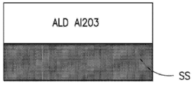
본원의 추가적인 양태는 스테인레스 강 구조체, 물질 또는 장치를 알루미나 코팅으로 코팅함을 포함하는, 사용되거나 작동될 때 할로겐화알루미늄에 노출되는 스테인레스 강 구조체, 물질 또는 장치의 내식성을 향상시키는 방법에 관한 것이다.A further aspect herein relates to a method of improving corrosion resistance of a stainless steel structure, material or device exposed to aluminum halide when used or in operation, comprising coating the stainless steel structure, material or device with an alumina coating.
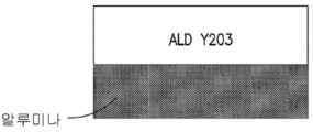
본원의 다른 양태는 사용되거나 작동될 때 에칭 매질에 노출되는 반도체 가공 에칭 구조체, 구성요소 또는 장치에 관한 것으로, 이 때 상기 구조체, 구성요소 또는 장치는 이트리아 층을 포함하는 코팅으로 코팅되고, 상기 이트리아 층은 임의적으로는 상기 코팅에서 알루미나 층 위에 놓인다.Another aspect of the present application relates to a semiconductor processing etch structure, component or device that is exposed to an etching medium when used or operated, wherein the structure, component or device is coated with a coating comprising an yttria layer, and wherein the The yttria layer optionally overlies the alumina layer in the coating.
본원의 또 다른 양태는 사용되거나 작동될 때 에칭 매질에 노출되는 반도체 가공 에칭 구조체, 구성요소 또는 장치의 내식성 및 에칭 저항성을 향상시키는 방법에 관한 것으로, 이 때 상기 방법은 이트리아 층을 포함하는 코팅으로 상기 구조체, 구성요소 또는 장치를 코팅함을 포함하고, 상기 이트리아 층은 임의적으로는 상기 코팅에서 알루미나 층 위에 놓인다.Another aspect of the present disclosure relates to a method of improving corrosion resistance and etching resistance of a semiconductor processed etch structure, component or device exposed to an etch medium when used or operated, wherein the method comprises a coating comprising an yttria layer With coating the structure, component or device, the yttria layer optionally overlying the alumina layer in the coating.
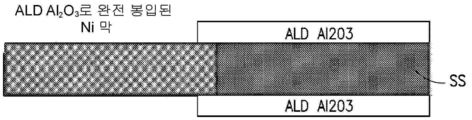
다른 양태에서, 본원은 알루미나 코팅으로 봉입된 니켈 막을 포함하는 에칭 챔버 확산판에 관한 것이다.In another aspect, the present application relates to an etching chamber diffuser plate comprising a nickel film encapsulated with an alumina coating.
본원의 추가적인 양태는 니켈 막을 알루미나의 봉입 코팅으로 코팅함을 포함하는, 니켈 막을 포함하는 에칭 챔버 확산판의 내식성 및 에칭 저항성을 향상시키는 방법에 관한 것이다.A further aspect of the present disclosure relates to a method of improving corrosion resistance and etching resistance of an etching chamber diffuser plate comprising a nickel film, comprising coating the nickel film with an encapsulating coating of alumina.
다른 양태에서, 본원은 사용되거나 작동될 때 할로겐화물 매질에 노출되는 증착 가공 구조체, 구성요소 또는 장치에 관한 것으로, 이 때 상기 구조체, 구성요소 또는 장치는 이트리아의 ALD 기본 코팅 및 이트리아의 PVD 상부 코팅(over coating)을 포함하는 이트리아의 코팅으로 코팅된다.In another aspect, the present application relates to a vapor deposition processing structure, component or device that is exposed to a halide medium when used or operated, wherein the structure, component or device is an ALD base coating of yttria and PVD of yttria. It is coated with a coating of yttria, including an over coating.
또 다른 양태에서, 본원은 이트리아의 ALD 기본 코팅 및 이트리아의 PVD 상부 코팅을 포함하는 이트리아의 코팅으로 구조체, 구성요소 또는 장치를 코팅함을 포함하는, 사용되거나 작동될 때 할로겐화물 매질에 노출되는 증착 가공 구조체, 구성요소 또는 장치의 내식성 및 에칭 저항성을 향상시키는 방법에 관한 것이다.In another aspect, the present application is directed to a halide medium when used or in operation comprising coating a structure, component or device with a coating of yttria comprising an ALD base coating of yttria and a PVD top coating of yttria. It relates to a method for improving the corrosion resistance and etching resistance of an exposed deposition processing structure, component or device.
본원의 또 다른 양태는 알루미나 확산 차단 층으로 내표면 상에서 코팅된 석영 봉입(envelope) 구조체에 관한 것이다.Another aspect of the present application relates to a quartz envelope structure coated on an inner surface with an alumina diffusion barrier layer.
본원의 추가적인 양태는 석영 봉입 구조체의 내표면을 알루미나 확산 차단 층으로 코팅함을 포함하는, 작동시에 수은 확산이 이루어지기 쉬운 석영 봉입 구조체 내로의 수은 확산을 감소시키는 방법에 관한 것이다.A further aspect of the present application relates to a method of reducing mercury diffusion into a quartz encapsulation structure where mercury diffusion is likely to occur in operation, comprising coating the inner surface of the quartz encapsulation structure with an alumina diffusion barrier layer.
본원의 또 다른 양태는 사용되거나 작동될 때 플라즈마 및 1000V가 넘는 전압에 노출되는 플라즈마 공급 구조체, 구성요소 또는 장치에 관한 것으로, 이 때 상기 구조체, 구성요소 또는 장치의 플라즈마-습윤되는 표면은 알루미나의 ALD 코팅으로 코팅되고, 상기 알루미나 코팅은 옥시질화알루미늄의 PVD 코팅으로 상부 코팅된다.Another aspect of the present application relates to a plasma supply structure, component or device that is exposed to a plasma and voltage above 1000 V when used or operated, wherein the plasma-wet surface of the structure, component or device is alumina. It is coated with ALD coating, and the alumina coating is top coated with PVD coating of aluminum oxynitride.
하나의 양태에서 본원은 사용되거나 작동될 때 플라즈마 및 1000V가 넘는 전압에 노출되는 플라즈마 공급 구조체, 구성요소 또는 장치의 사용 수명을 향상시키는 방법에 관한 것으로, 이 때 상기 방법은 상기 구조체, 구성요소 또는 장치의 플라즈마-습윤되는 표면을 알루미나의 ALD 코팅으로 코팅하고, 상기 알루미나 코팅을 옥시질화알루미늄의 PVD 코팅으로 상부 코팅함을 포함한다.In one aspect, the present application relates to a method of improving the service life of a plasma supply structure, component or device that is exposed to a plasma and a voltage in excess of 1000 V when used or operated, wherein the method comprises: And coating the plasma-wet surface of the device with an ALD coating of alumina, and top coating the alumina coating with a PVD coating of aluminum oxynitride.
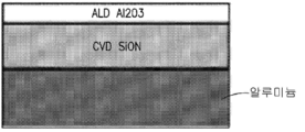
본원은 다른 양태에서 알루미나의 기본 층, 그 위의 니켈 전극 층, 니켈 전극 층 위의 ALD 알루미나 전기 격리(stand-off) 층, ALD 알루미나 전기 격리 층 위의 PVD 옥시질화알루미늄 열 팽창 완충 층, 및 PVD 옥시질화알루미늄 열 팽창 완충 층 위의 CVD 옥시질화규소 웨이퍼 접촉 표면 및 전기 스페이서 층을 포함하는 유전성 적층체(dielectric stack)에 관한 것이다.In another aspect, the present disclosure provides a base layer of alumina, a nickel electrode layer thereon, an ALD alumina electrical stand-off layer over the nickel electrode layer, a PVD aluminum oxynitride thermal expansion buffer layer over the ALD alumina electrical isolation layer, and A dielectric stack comprising an electrical spacer layer and an CVD silicon oxynitride wafer contact surface over a PVD aluminum oxynitride thermal expansion buffer layer.
본원은 다른 양태에서 하기 다층 코팅중 하나로 코팅된 알루미늄 표면을 포함하는 플라즈마 활성화 구조체, 구성요소 또는 장치에 관한 것이다: (i) 알루미늄 표면 상의 CVD 규소의 기본 코팅, 및 CVD 규소의 기본 코팅 위의 ALD 지르코니아 층, 및 (ii) 알루미늄 표면 상의 CVD 옥시질화규소 기본 코팅, 및 CVD 옥시질화규소 기본 코팅 상의 ALD 알루미나 층.The present application relates to a plasma activated structure, component or device comprising an aluminum surface coated with one of the following multilayer coatings in another aspect: (i) a base coating of CVD silicon on an aluminum surface, and an ALD over base coating of CVD silicon Zirconia layer, and (ii) CVD silicon oxynitride base coating on aluminum surface, and ALD alumina layer on CVD silicon oxynitride base coating.
본원의 또 다른 양태는 하기 다층 코팅중 하나로 알루미늄 표면을 코팅함을 포함하는, 플라즈마 활성화 구조체, 구성요소 또는 장치의 알루미늄 표면의 입자 형성 및 금속 오염을 감소시키는 방법에 관한 것이다: (i) 알루미늄 표면 상의 CVD 규소의 기본 코팅, 및 CVD 규소의 기본 코팅 위의 ALD 지르코니아 층, 및 (ii) 알루미늄 표면 상의 CVD 옥시질화규소 기본 코팅, 및 CVD 옥시질화규소 기본 코팅 상의 ALD 알루미나 층.Another aspect of the present application relates to a method of reducing particle formation and metal contamination of an aluminum surface of a plasma activated structure, component or device comprising coating an aluminum surface with one of the following multilayer coatings: (i) aluminum surface Basic coating of CVD silicon on top, and ALD zirconia layer over basic coating of CVD silicon, and (ii) CVD silicon oxynitride basic coating on aluminum surface, and ALD alumina layer on CVD silicon oxynitride basic coating.
다공성 매트릭스 필터가 본원의 다른 양태에서 고려되는데, 상기 다공성 매트릭스 필터는 스테인레스 강, 니켈 또는 티탄으로 이루어진 막을 포함하고, 상기 막은 20 내지 2000㎛의 코팅 침투 깊이까지 알루미나로 봉입된다.A porous matrix filter is contemplated in another aspect of the present application, wherein the porous matrix filter comprises a membrane made of stainless steel, nickel or titanium, and the membrane is sealed with alumina to a coating penetration depth of 20 to 2000 μm.
상응하는 방법 양태에서, 본원은 스테인레스 강, 니켈 또는 티탄으로 이루어진 막을 20 내지 2000㎛의 코팅 침투 깊이까지 알루미나로 봉입시킴을 포함하는, 다공성 매트릭스 필터를 제조하는 방법에 관한 것이다.In a corresponding method aspect, the present application relates to a method of making a porous matrix filter comprising encapsulating a membrane made of stainless steel, nickel or titanium with alumina to a coating penetration depth of 20 to 2000 μm.
본원의 다른 양태, 특징 및 실시양태는 뒤이은 상세한 설명 및 첨부된 특허청구범위로부터 더욱 충분히 명백해질 것이다.Other aspects, features, and embodiments herein will become more fully apparent from the detailed description that follows and the appended claims.
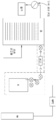
도 1은 본원의 한 양태에 따른 반도체 웨이퍼 가공 도구의 침착로의 개략도이다.
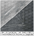
도 2는 AlCl3를 기화시켜 Al2Cl6 증기를 형성하기 위한 앰풀 형태로 고체 공급원 전달 기화기를 이용하는, Al2Cl6 증기를 사용하여 웨이퍼를 코팅하기 위한 본원의 다른 양태에 따른 침착로 공정 시스템의 개략도이며, 여기에서 앰풀의 트레이 및 내표면은 Al2O3로 코팅되고 또한 앰풀의 밸브, 관 및 필터도 모두 Al2O3로 코팅된다.
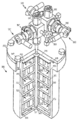
도 3은 홀더에 의해 지지되는 물질로부터의 증기와 기체의 접촉을 촉진시키기 위하여 홀더를 갖는 기화기 용기의 부분 절단 사시도이다.
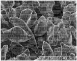
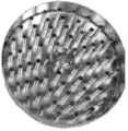
도 4는 본원의 다른 양태에 따라 필터 요소에 유용하게 사용되는 유형의 다공성 금속 프릿(frit) 표면의 15K 배율의 현미경 사진이다.
도 5는 AlCl3에 노출되지 않은 전해 연마된 316L 스테인레스 강의 표면의 20,000배 배율의 현미경 사진이다.
도 6은 무수성 환경에서 120℃에서 10일동안 AlCl3에 노출시킨 후 전해 연마된 316L 스테인레스 강 표면의 1000배 배율의 현미경 사진이다.
도 7은 AlCl3에 노출되지 않은 전해 연마된 316L 스테인레스 강의 단면의 50,000배 배율의 현미경 사진이다.
도 8은 무수성 환경에서 120℃에서 AlCl3에 10일간 노출된 후 코팅되지 않은 316L 스테인레스 강의 20,000배 배율의 현미경 사진이다.
도 9는 표면을 따라 다수개의 피트(pit)를 보여주는, 무수성 환경에서 120℃에서 AlCl3에 10일간 노출된 후 전해 연마된 316L 스테인레스 강의 35,000배 배율의 현미경 사진이다.
도 10은 10일동안 120℃에서 무수 AlCl3에 노출되기 전에, 트리메틸 알루미늄 및 물을 사용하여 Al2O3의 100 ALD 사이클에 의해 코팅된 전해 연마된 316L 스테인레스 강의 35,000배 배율의 현미경 사진이다.
도 11은 10일동안 120℃에서 무수 AlCl3에 노출되기 전에, 트리메틸 알루미늄 및 물을 사용하여 Al2O3의 1000 ALD 사이클에 의해 코팅된 전해 연마된 316L 스테인레스 강의 35,000배 배율의 현미경 사진이다.
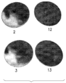
도 12는 155℃에서 AlCl3에 9일간 노출된 후 사진을 찍은, 샘플 스테인레스 강 쿠폰(샘플 쿠폰 2 및 3은 470Å 두께의 알루미나 코팅으로 코팅되고, 샘플 쿠폰 12 및 13은 코팅되지 않음)의 합성 사진이다.
도 13은 10일동안 220℃에서 WCl5에 노출된 후 알루미나-코팅된 스테인레스 강 샘플의 상부-하향 주사 전자 현미경(SEM) 현미경사진이다.
도 14는 10일동안 220℃에서 WCl5에 노출된 후 도 13의 샘플중 코팅 가장자리의 집속 이온 빔(FIB) 단면이다.
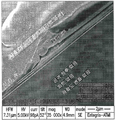
도 15는 알루미늄 공정에서 삼염화알루미늄(AlCl3) 고체 전구체 전달을 위해 기화기 앰풀에 유용하게 사용되는 스테인레스 강 홀더의 사시도이며, 여기에서 삼염화알루미늄 전구체는 홀더에 의해 지지되고 기화되어, 기화기 앰풀로부터 방출하기 위하여 또한 알루미늄 공정으로의 관련 유동 회로를 통해 수송하기 위하여 삼염화알루미늄 전구체 증기를 형성시킨다.
도 16은 기화기 앰풀의 사용 및 작동시에 홀더가 겪게 되는 삼염화알루미늄(AlCl3) 노출을 포함하는 부식성 환경에서 알루미나 코팅에 의해 스테인레스 강 표면이 봉입되도록 알루미나 코팅으로 원자 층 침착에 의해 코팅된 도 15에 도시된 유형의 스테인레스 강 홀더의 사시도이다.
도 17은 내식성을 제공하고 기판과의 화학 반응을 방지하며 사용시 금속 오염을 감소시키기 위하여, 스테인레스 강 기판에 원자 층 침착에 의해 도포되는 알루미나 코팅의 개략적인 입면도이다.
도 18은 이트리아(Y2O3)로 코팅된 플라즈마 에칭 장치의 채널을 도시한다.
도 19는 알루미나 위에 원자 층 침착에 의해 도포되는 이트리아 코팅의 개략적인 입면도이다.
도 20은 알루미나 코팅으로 코팅된, 스테인레스 강 프레임 및 니켈 필터 막을 포함하는 확산판 어셈블리의 사진이다.
도 21은 스테인레스 강 프레임 및 니켈 막이 ALD 알루미나로 봉입된 확산판 어셈블리의 개략적인 입면도이다.
도 22는 알루미늄 기판, 알루미나의 ALD 코팅, 및 AlON의 PVD 코팅을 포함하는 코팅 구조체의 개략적인 입면도이다.
도 23은 알루미나 기판이 그 위에 전극 금속을 갖고, 그 위에 ALD 알루미나의 전기 격리 층이 있으며, 그 위에 옥시질화알루미늄의 PVD 코팅이 있고, 그 위에 화학적 증착(CVD) 침착된 옥시질화규소(SiON) 층이 있는, 고온 척(hot chuck) 구성요소에 유용한 유전성 적층체의 층 구조의 개략적인 입면도이다.
도 24는 CVD Si 층 위에 지르코니아의 ALD 층이 있는, 알루미늄 기판 상의 규소의 화학적 증착-도포된 층을 포함하는 다층 적층체의 개략적인 입면도이다.
도 25는 알루미늄 기판 상의 옥시질화규소의 CVD 층 및 CVD SiON 코팅 층 상의 알루미나의 ALD 층을 포함하는 다층 적층체의 개략적인 입면도이다.
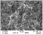
도 26은 전자 층 침착에 의해 알루미나로 코팅된, 1.5mm 벽 두께 및 2 내지 4㎛의 공극 크기를 갖는 다공성 물질의 현미경 사진이다.
도 27은 ALD에 의해 침착된 알루미나로 완전히 봉입된, 스테인레스 강, 니켈, 티탄 또는 다른 적합한 물질로 이루어진 막을 포함하는 봉입된 막의 개략도이다.
도 28은 코팅이 35㎛의 코팅 침투 깊이를 갖는 알루미나인, 코팅된 필터의 현미경 사진이다.
도 29는 코팅이 175㎛의 코팅 침투 깊이를 갖는 알루미나인, 코팅된 필터의 현미경 사진이다.1 is a schematic diagram of a deposition furnace of a semiconductor wafer processing tool according to one aspect of the present application.
2 is AlCl 3 vaporization by Al 2 Cl to 6 ampoule form for forming a vapor using a solid source delivery carburetor, the process system to a deposition according to a further aspect of the present application for coating a wafer with a Al 2 Cl 6 Steam A schematic diagram of the ampoule, wherein the tray and inner surface of the ampoule are coated with Al 2 O 3 , and the valves, tubes and filters of the ampoule are all coated with Al 2 O 3 .
3 is a partially cut-away perspective view of a vaporizer container having a holder to facilitate contact of vapor and gas from the material supported by the holder.
4 is a micrograph of 15K magnification of a porous metal frit surface of the type useful for filter elements according to another aspect of the present application.
FIG. 5 is a photomicrograph of 20,000 times magnification of the surface of an electropolished 316L stainless steel not exposed to AlCl 3 .
FIG. 6 is a micrograph of 1000x magnification of an electropolished 316L stainless steel surface after exposure to AlCl 3 for 10 days at 120° C. in an anhydrous environment.
FIG. 7 is a photomicrograph of a magnification of 50,000 times the cross section of an electropolished 316L stainless steel not exposed to AlCl 3 .
8 is a micrograph of 20,000 times magnification of uncoated 316L stainless steel after being exposed to AlCl 3 for 10 days at 120° C. in an anhydrous environment.
9 is a micrograph of 35,000 times magnification of electrolytically polished 316L stainless steel after 10 days of exposure to AlCl 3 at 120° C. in an anhydrous environment, showing multiple pits along the surface.
FIG. 10 is a microscope picture of 35,000 times magnification of electropolished 316L stainless steel coated by 100 ALD cycles of Al 2 O 3 with trimethyl aluminum and water before exposure to anhydrous AlCl 3 at 120° C. for 10 days.
FIG. 11 is a microscope picture of 35,000 times magnification of electropolished 316L stainless steel coated by 1000 ALD cycles of Al 2 O 3 with trimethyl aluminum and water before exposure to anhydrous AlCl 3 at 120° C. for 10 days.
FIG. 12 is a synthesis of sample stainless steel coupons (
13 is a top-down scanning electron microscope (SEM) micrograph of an alumina-coated stainless steel sample after exposure to WCl 5 at 220° C. for 10 days.
14 is a focused ion beam (FIB) cross-section of the coating edge of the sample of FIG. 13 after exposure to WCl 5 at 220° C. for 10 days.
15 is a perspective view of a stainless steel holder useful for use in a vaporizer ampoule for the delivery of an aluminum trichloride (AlCl 3 ) solid precursor in an aluminum process, wherein the aluminum trichloride precursor is supported and vaporized by a holder to release from the vaporizer ampoule In order to also transport the aluminum trichloride precursor vapor for transport through the relevant flow circuit to the aluminum process.
FIG. 16 is coated by atomic layer deposition with alumina coating such that the stainless steel surface is encapsulated by alumina coating in a corrosive environment that includes aluminum trichloride (AlCl 3 ) exposure experienced by the holder during use and operation of the vaporizer ampoule. Is a perspective view of a stainless steel holder of the type shown in.
17 is a schematic elevational view of an alumina coating applied by atomic layer deposition on a stainless steel substrate to provide corrosion resistance, prevent chemical reactions with the substrate, and reduce metal contamination in use.
18 shows a channel of a plasma etching apparatus coated with yttria (Y 2 O 3 ).
19 is a schematic elevational view of an yttria coating applied by atomic layer deposition over alumina.
20 is a photograph of a diffuser plate assembly comprising a stainless steel frame and a nickel filter membrane, coated with an alumina coating.
21 is a schematic elevational view of a diffuser plate assembly in which a stainless steel frame and nickel film are sealed with ALD alumina.
22 is a schematic elevational view of a coating structure comprising an aluminum substrate, an ALD coating of alumina, and a PVD coating of AlON.
FIG. 23 shows an alumina substrate with an electrode metal thereon, an electrical isolation layer of ALD alumina thereon, a PVD coating of aluminum oxynitride thereon, and a silicon oxynitride (SiON) layer deposited thereon by chemical vapor deposition (CVD) This is a schematic elevational view of the layer structure of a dielectric laminate useful for hot chuck components.
24 is a schematic elevational view of a multi-layer laminate comprising a chemical vapor-deposited layer of silicon on an aluminum substrate, with an ALD layer of zirconia over the CVD Si layer.
25 is a schematic elevational view of a multi-layer laminate comprising a CVD layer of silicon oxynitride on an aluminum substrate and an ALD layer of alumina on a CVD SiON coating layer.
FIG. 26 is a micrograph of a porous material coated with alumina by electron layer deposition, having a 1.5 mm wall thickness and a pore size of 2 to 4 μm.
27 is a schematic view of an encapsulated membrane comprising a membrane made of stainless steel, nickel, titanium, or other suitable material, completely encapsulated with alumina deposited by ALD.
28 is a micrograph of the coated filter, wherein the coating is alumina with a coating penetration depth of 35 μm.
29 is a micrograph of the coated filter, wherein the coating is alumina with a coating penetration depth of 175 μm.
본 발명은 일반적으로 다양한 기판 제품, 물질, 구조체 및 설비에 도포될 수 있는 코팅에 관한 것이다. 다양한 양태에서, 본원은 반도체 제조 설비 및 그의 성능을 향상시키는 방법에 관한 것이고, 더욱 구체적으로는 반도체 제조 설비에서 육염화이알루미늄의 존재에 수반되는 오염 및 입자 침착이 일어나기 쉬운 이러한 반도체 제조 설비, 및 이러한 불리한 오염 및 입자 침착에 대항할 수 있는 조성물 및 방법에 관한 것이다.The present invention relates generally to coatings that can be applied to a variety of substrate products, materials, structures and equipment. In various aspects, the present application relates to a semiconductor manufacturing facility and a method for improving its performance, and more specifically, such a semiconductor manufacturing facility that is susceptible to contamination and particle deposition accompanying the presence of aluminum hexachloride in the semiconductor manufacturing facility, and It relates to compositions and methods that can combat adverse contamination and particle deposition.
본원에 사용되는 경우, 예컨대 C1-C12 알킬에서 탄소 수 범위의 표시는, 이 언급된 범위에서 각각의 중간에 끼이는 탄소 수 및 임의의 다른 언급되거나 중간에 끼인 탄소 수 값이 포괄되도록, 이러한 범위 내의 구성 탄소 수 일부분 각각을 포함하고자 하며, 명시된 탄소 수 범위 내의 탄소 수의 부분 범위는 본 발명의 영역 내에서 더 작은 탄소 수 범위에 독립적으로 포함될 수 있고 탄소 수 또는 수들을 특정적으로 배제하는 탄소 수의 범위가 본 발명에 포함되며 명시된 범위의 탄소 수 한도중 어느 하나 또는 둘 다를 배제하는 부분 범위도 본 발명에 포함되는 것으로 생각된다. 따라서, C1-C12 알킬은 메틸, 에틸, 프로필, 부틸, 펜틸, 헥실, 헵틸, 옥틸, 노닐, 데실, 운데실 및 도데실(이러한 유형의 직쇄뿐만 아니라 분지된 기도 포함함)을 포함하고자 한다. 그러므로, 치환기 잔기에 넓게 적용될 수 있는 탄소 수 범위의 표시, 예를 들어 C1-C12는 본 발명의 특정 실시양태에서 탄소 수 범위가 치환기 잔기의 더 넓은 내역 내의 탄소 수 범위를 갖는 잔기의 부분집합으로서 추가로 제한되게 할 수 있음을 알아야 한다. 예로서, 탄소수 범위, 예컨대 C1-C12 알킬은 본 발명의 특정 실시양태에서 C1-C4 알킬, C2-C8 알킬, C2-C4 알킬, C3-C5 알킬 또는 넓은 탄소 수 범위 내의 임의의 다른 부분 범위를 포괄하도록 더욱 제한적으로 명시될 수 있다. 달리 말해, 탄소 수 범위는 이러한 범위가 적용되는 치환기, 잔기 또는 화합물에 대해서 이 범위의 탄소 수 종류 각각을 선택 군(이로부터 선택 군의 일원중 특정적인 하나가 연속적인 탄소 수 부분 범위로서 또는 이러한 선택 군 내의 특정 탄소 수 종류로서 선택될 수 있음)으로서 확정적으로 기재하는 것으로 간주된다. As used herein, an indication of a carbon number range, such as in C 1 -C 12 alkyl, is intended to cover the carbon number values interposed between each other and any other mentioned or intervened carbon number values in this stated range, It is intended to include each of the constituent carbon number portions within this range, and a partial range of carbon numbers within the specified carbon number range may be independently included in a smaller carbon number range within the scope of the present invention and specifically exclude carbon numbers or numbers. It is contemplated that ranges of carbon numbers to be included in the present invention and subranges excluding either or both of the carbon number limits in the specified ranges are also included in the present invention. Thus, C 1 -C 12 alkyl is intended to include methyl, ethyl, propyl, butyl, pentyl, hexyl, heptyl, octyl, nonyl, decyl, undecyl and dodecyl (including straight chains of this type as well as branched airways). do. Therefore, an indication of a carbon number range that can be broadly applied to a substituent residue, e.g., C 1 -C 12, is a portion of a residue having a carbon number range within a broader specification of the substituent residues in certain embodiments of the present invention. It should be noted that it can be further restricted as a set. By way of example, a carbon number range, such as C 1 -C 12 alkyl, in certain embodiments of the invention C 1 -C 4 alkyl, C 2 -C 8 alkyl, C 2 -C 4 alkyl, C 3 -C 5 alkyl or broad It can be more restrictively specified to cover any other subrange within the carbon number range. In other words, the carbon number range is selected from each of the carbon number types of this range for the substituent, residue or compound to which this range applies, from which a specific one of the members of the selection group is a continuous carbon number subrange or such It can be selected as a specific carbon number type in the selected group).
명시된 범위, 수치 값 제한(예를 들어, 동일하지 않음, 제한보다 더 큼, 더 작음)뿐만 아니라, 산화 상태 및 특정 형태, 전하 상태 및 본원의 넓은 영역 내에서 도판트 공급원, 주입 물질 및 화합물에 적용될 수 있는 조성을 결정하는 다른 변수에 대해서 화학량론적 계수 및 원자, 작용기, 이온 또는 잔기의 수를 명시하는 수치 값에 동일한 구성 및 선택 융통성이 적용될 수 있다. Specified ranges, numerical value limits (e.g., not equal, greater than, less than limit), as well as oxidation states and specific forms, charge states, and dopant sources, implant materials and compounds within a broad range herein The same configuration and selection flexibility can be applied to stoichiometric coefficients and numerical values specifying the number of atoms, functional groups, ions or moieties for other variables that determine the composition that can be applied.
본원에 사용되는 "알킬"은 메틸, 에틸, 프로필, 이소프로필, 부틸, s-부틸, t-부틸, 펜틸 및 이소펜틸 등을 포함하지만 이들로 한정되지는 않는다. 본원에 사용되는 "아릴"은 탄소 원자 6 내지 10개의 불포화 방향족 탄소환상 기인 벤젠 또는 벤젠 유도체로부터 유도되는 탄화수소를 포함한다. 아릴은 단일 고리 또는 다중 고리를 가질 수 있다. 본원에 사용되는 용어 "아릴"은 치환된 아릴도 포함한다. 예는 페닐, 나프틸, 자일렌, 페닐에탄, 치환된 페닐, 치환된 나프틸, 치환된 자일렌, 치환된 페닐에탄 등을 포함하지만, 이들로 국한되지는 않는다. 본원에 사용되는 "사이클로알킬"은 사이클로프로필, 사이클로부틸, 사이클로펜틸, 사이클로헥실 등을 포함하지만, 이들로 한정되지는 않는다. 본원의 모든 화학식에서, 탄소 수의 범위는 명시된 범위에서 탄소 수의 종결점 값 중간의 탄소 원자의 수를 함유하는 모든 잔기 및 특정 범위의 종결점 값과 동일한 탄소 원자의 수를 함유하는 잔기를 포함하여 일련의 연속적인 다른 탄소-함유 잔기를 명시하는 것으로 간주되는데, 예를 들어 C1-C6은 C1, C2, C3, C4, C5 및 C6을 포함하고, 이러한 더 넓은 범위 각각은 그의 부분 범위로서 이러한 범위 내의 탄소 수를 참조하여 추가로 한정적으로 명시될 수 있다. 그러므로, 예를 들어 범위 C1-C6은 더 넓은 범위의 영역 내의 C1-C3, C1-C4, C2-C6, C4-C6 등과 같은 부분 범위를 포함하고 이러한 부분 범위를 명시함으로써 추가로 한정될 수 있다. As used herein, "alkyl" includes, but is not limited to, methyl, ethyl, propyl, isopropyl, butyl, s-butyl, t-butyl, pentyl and isopentyl, and the like. As used herein, "aryl" includes hydrocarbons derived from benzene or benzene derivatives having 6 to 10 unsaturated aromatic carbocyclic groups. Aryl can have a single ring or multiple rings. As used herein, the term "aryl" also includes substituted aryl. Examples include, but are not limited to, phenyl, naphthyl, xylene, phenylethane, substituted phenyl, substituted naphthyl, substituted xylene, substituted phenylethane, and the like. “Cycloalkyl” as used herein includes, but is not limited to, cyclopropyl, cyclobutyl, cyclopentyl, cyclohexyl, and the like. In all of the formulas herein, the range of carbon numbers includes all residues containing the number of carbon atoms in the range of the carbon number's endpoint value in the specified range and residues containing the same number of carbon atoms as the specific range of endpoint values. It is considered to indicate a series of other carbon-containing residues in series, for example C 1 -C 6 includes C 1 , C 2 , C 3 , C 4 , C 5 and C 6 , and these broader Each of the ranges can be further limitedly specified by referring to the number of carbons within these ranges as their subranges. Thus, for example, the range C 1 -C 6 includes subranges such as C 1 -C 3 , C 1 -C 4 , C 2 -C 6 , C 4 -C 6 and the like within a wider range of regions, and such portions It can be further limited by specifying the scope.
본원은 한 양태에서 금속의 산화물, 질화물 또는 할로겐화물(플루오르화물, 염화물, 요오드화물 및/또는 브롬화물)이 형성되기 쉬운 금속 표면이 반응성 기체와 코팅된 표면의 반응을 방지하는 보호 코팅으로 코팅되는, 금속의 산화물, 질화물 또는 할로겐화물(플루오르화물, 염화물, 요오드화물 및/또는 브롬화물)이 형성되기 쉬운 금속 표면을 포함하는 구조체, 물질 또는 장치에 관한 것이며, 이 때 상기 금속 표면은 이러한 구조체, 물질 또는 장치의 사용 또는 작동시에 상기 금속 산화물, 질화물 또는 할로겐화물과 반응성이어서 구조체, 물질 또는 장치 및 그의 사용 또는 작동에 유해한 반응 생성물을 생성시키는 기체, 고체 또는 액체와 접촉되도록 구성되어 있다. Herein, in one aspect, metal surfaces prone to the formation of oxides, nitrides or halides (fluoride, chloride, iodide and/or bromide) of the metal are coated with a protective coating that prevents the reaction of the reactive gas with the coated surface, A structure, material or device comprising a metal surface prone to the formation of oxides, nitrides or halides of metals (fluoride, chloride, iodide and/or bromide), wherein the metal surface is such a structure, material or It is configured to be in contact with the metal oxide, nitride or halide during use or operation of the device, thereby contacting a structure, material or device and a gas, solid or liquid that produces a reaction product harmful to its use or operation.
하나의 양태에서, 본원은 금속의 산화물, 질화물 또는 할로겐화물이 형성되기 쉬운 금속 표면이 반응성 기체와 코팅된 표면의 반응을 방지하는 보호 코팅으로 코팅되는, 금속의 산화물, 질화물 또는 할로겐화물이 형성되기 쉬운 금속 표면을 포함하는 반도체 제조 장치에 관한 것이며, 이 때 상기 금속 표면은 이러한 장치의 사용 또는 작동시에 상기 금속과 반응성이어서 장치 및 그의 사용 또는 작동에 유해한 반응 생성물을 생성시키는 기체, 고체 또는 액체와 접촉되도록 구성되어 있다. In one aspect, an oxide, nitride or halide of a metal is formed herein, wherein a metal surface prone to formation of an oxide, nitride or halide of the metal is coated with a protective coating that prevents the reaction of the reactive gas with the coated surface. It relates to a semiconductor manufacturing apparatus comprising an easy metal surface, wherein the metal surface is reactive with the metal during use or operation of such a device to produce a gas, solid or liquid that is hazardous to the device and its use or operation. It is configured to contact with.
이러한 반도체 제조 장치에서, 금속 산화물은 다양한 실시양태에서 Cr, Fe, Co 및 Ni중 하나 이상의 하나 이상의 산화물을 포함할 수 있거나, 또는 다른 실시양태에서 금속 산화물은 Cr, Fe 및 Ni중 하나 이상의 하나 이상의 산화물을 포함할 수 있다. 금속 질화물은 예를 들어 암모니아가 존재할 때 가공 동안 암모니아의 존재하에 철 또는 코발트로부터 형성될 수 있으며, 생성되는 질화철 또는 질화코발트는 이어 AlCl3 또는 TiCl4와 반응한다. 금속 할로겐화물은 에칭 공정 또는 세정 사이클 작업 동안 금속 표면 상에 형성될 수 있다. 다양한 실시양태에서 금속 표면은 스테인레스 강 표면을 포함할 수 있다. 특정 실시양태에서, 금속 산화물, 질화물 또는 할로겐화물과 반응성이어서 장치 및 그의 사용 또는 작동에 유해한 반응 생성물을 생성시키는 기체는 Al2Cl6를 포함한다.In such a semiconductor manufacturing apparatus, the metal oxide may include one or more oxides of Cr, Fe, Co, and Ni in various embodiments, or in other embodiments the metal oxide may be one or more of Cr, Fe, and Ni. Oxides. Metal nitrides can be formed from iron or cobalt in the presence of ammonia during processing when, for example, ammonia is present, and the resulting iron nitride or cobalt nitride then reacts with AlCl 3 or TiCl 4 . Metal halides may be formed on the metal surface during the etching process or cleaning cycle operation. In various embodiments the metal surface can include a stainless steel surface. In certain embodiments, the gas that is reactive with the metal oxide, nitride, or halide to produce a reaction product harmful to the device and its use or operation includes Al 2 Cl 6 .
특정 용도에서 보호 코팅은 Al2O3, 화학식 MO(여기에서, M은 Ca, Mg 또는 Be임)의 산화물, 화학식 M'O2(여기에서, M'은 화학량론적으로 허용가능한 금속임)의 산화물, 및 화학식 Ln2O3(여기에서, Ln은 란탄족 원소, 예를 들어 La, Sc 또는 Y임)의 산화물로 이루어진 군으로부터 선택되는 코팅 물질중 하나 이상을 포함할 수 있다. 더욱 일반적으로, 보호 코팅은 장치의 작동시 금속 표면과 접촉하는 물질과의 반응의 자유 에너지가 0 이상인 금속 산화물을 포함할 수 있다. In certain applications the protective coating is of Al 2 O 3 , an oxide of the formula MO (where M is Ca, Mg or Be), of the formula M'O 2 (where M'is a stoichiometrically acceptable metal). Oxide, and a coating material selected from the group consisting of oxides of the formula Ln 2 O 3 (where Ln is a lanthanide element, such as La, Sc or Y). More generally, the protective coating may include a metal oxide in which the free energy of reaction with a material in contact with the metal surface during operation of the device is zero or more.
본원의 추가적인 양태는 금속의 산화물, 질화물 또는 할로겐화물이 형성되기 쉬운 금속 표면을 반응성 기체와 코팅된 표면의 반응을 방지하는 보호 코팅으로 코팅함을 포함하는, 금속의 산화물, 질화물 또는 할로겐화물이 형성되기 쉬운 금속 표면을 포함하는 구조체, 물질 또는 장치의 성능을 개선하는 방법에 관한 것이며, 이 때 상기 금속 표면은 이러한 구조체, 물질 또는 장치의 사용 또는 작동시에 상기 금속 산화물, 질화물 또는 할로겐화물과 반응성이어서 구조체, 물질 또는 장치 및 그의 사용 또는 작동에 유해한 반응 생성물을 생성시키는 기체, 고체 또는 액체와 접촉되도록 구성되어 있다.An additional aspect of the present application includes forming a metal oxide, nitride, or halide, which is prone to formation of an oxide, nitride, or halide of the metal with a protective coating that prevents the reaction of the reactive gas with the coated surface. A method for improving the performance of a structure, material or device comprising a prone metal surface, wherein the metal surface is reactive with the metal oxide, nitride or halide in use or operation of such structure, material or device It is then configured to contact structures, materials or devices and gases, solids or liquids that produce reaction products harmful to their use or operation.
다른 양태에서, 본원은 금속의 산화물, 질화물 또는 할로겐화물이 형성되기 쉬운 금속 표면을 반응성 기체와 코팅된 표면의 반응을 방지하는 보호 코팅으로 코팅함을 포함하는, 금속의 산화물, 질화물 또는 할로겐화물이 형성되기 쉬운 금속 표면을 포함하는 반도체 제조 장치의 성능을 개선하는 방법에 관한 것이며, 이 때 상기 금속 표면은 이러한 장치의 사용 또는 작동시에 상기 금속 산화물, 질화물 또는 할로겐화물과 반응성이어서 장치 및 그의 사용 또는 작동에 유해한 반응 생성물을 생성시키는 기체와 접촉되도록 구성되어 있다.In another aspect, the present disclosure includes oxide, nitride or halide of a metal comprising coating a metal surface prone to formation of oxide, nitride or halide of the metal with a protective coating that prevents the reaction of the reactive gas with the coated surface. It relates to a method for improving the performance of a semiconductor manufacturing apparatus comprising a metal surface that is likely to be formed, wherein the metal surface is reactive with the metal oxide, nitride or halide during use or operation of such a device, and the device and use thereof Or is configured to come into contact with a gas that produces a reaction product that is harmful to operation.
다양한 실시양태에서 금속 산화물, 질화물 또는 할로겐화물은 Cr, Fe, Co 및 Ni중 하나 이상의 하나 이상의 산화물, 질화물 또는 할로겐화물을 포함할 수 있고, 다른 실시양태에서는 Cr, Fe 및 Ni중 하나 이상의 하나 이상의 산화물, 질화물 또는 할로겐화물, 또는 임의의 다른 적합한 금속 산화물, 질화물 또는 할로겐화물 물질을 포함할 수 있다. 금속 표면은 예를 들어 스테인레스 강을 포함할 수 있다. 금속 산화물, 질화물 또는 할로겐화물과 반응성이어서 구조체, 물질 또는 장치 및 그의 사용 또는 작동에 유해한 반응 생성물을 형성하는 기체는 Al2Cl6를 포함할 수 있다. In various embodiments the metal oxide, nitride or halide may include one or more oxides, nitrides or halides of Cr, Fe, Co and Ni, and in other embodiments one or more of Cr, Fe and Ni Oxide, nitride or halide, or any other suitable metal oxide, nitride or halide material. The metal surface may include stainless steel, for example. Gases that are reactive with metal oxides, nitrides or halides to form structures, materials or devices and reaction products harmful to their use or operation may include Al 2 Cl 6 .
전술한 방법에서 금속 표면에 도포되는 보호 코팅은 Al2O3, 화학식 MO(여기에서, M은 Ca, Mg 또는 Be임)의 산화물, 화학식 M'O2(여기에서, M'은 화학량론적으로 허용가능한 금속임)의 산화물, 및 화학식 Ln2O3(여기에서, Ln은 란탄족 원소, 예를 들어 La, Sc 또는 Y임)의 산화물로 이루어진 군으로부터 선택되는 코팅 물질중 하나 이상을 포함할 수 있다. 더욱 일반적으로, 보호 코팅은 상기 구조체, 물질 또는 장치의 사용 또는 작동시 금속 표면과 접촉하는 기체와의 반응의 자유 에너지가 0 이상인 금속 산화물을 포함할 수 있다. In the above-described method, the protective coating applied to the metal surface is Al 2 O 3 , an oxide of the formula MO (where M is Ca, Mg or Be), and the formula M'O 2 (where M'is stoichiometrically Oxide of an acceptable metal), and a coating material selected from the group consisting of oxides of the formula Ln 2 O 3 (where Ln is a lanthanide element, for example La, Sc or Y) Can. More generally, the protective coating may include a metal oxide in which the free energy of reaction with a gas contacting the metal surface during use or operation of the structure, material or device is zero or more.
보호 코팅은 임의의 적합한 기법에 의해 본원의 방법에서 금속 표면에 도포될 수 있으며, 특정 용도에서 코팅 작업은 보호 코팅의 물리적 증착(PVD), 화학적 증착(CVD), 용액 침착, 또는 원자 층 침착(ALD)을 포함할 수 있다. The protective coating may be applied to the metal surface in the methods herein by any suitable technique, and in certain applications the coating operation may include physical deposition (PVD), chemical vapor deposition (CVD), solution deposition, or atomic layer deposition of the protective coating ( ALD).
ALD는 금속 표면에 보호 코팅을 도포하기에 바람직한 기법이다. 특정 용도에서, 플라즈마-향상 ALD는 금속 표면 상에 보호 코팅을 형성시키기 위한 ALD 방법으로서 아용될 수 있다. 다양한 ALD 실시양태에서, 보호 코팅은 Al2O3를 포함할 수 있다. 이러한 보호 코팅은 예컨대 트리메틸알루미늄과 오존이 순환 ALD 공정에 사용되어 보호 코팅을 형성하는 일련의 공정을 포함하는 원자 층 침착에 의해, 또는 다르게는 트리메틸알루미늄과 물이 순환 ALD 공정에 사용되어 보호 코팅을 형성하는 일련의 공정을 포함하는 원자 층 침착에 의해 도포될 수 있다. ALD is the preferred technique for applying a protective coating to a metal surface. In certain applications, plasma-enhanced ALD can be utilized as an ALD method to form a protective coating on a metal surface. In various ALD embodiments, the protective coating can include Al 2 O 3 . Such protective coatings are, for example, by atomic layer deposition comprising a series of processes in which trimethylaluminum and ozone are used in a circulating ALD process to form a protective coating, or alternatively trimethylaluminum and water are used in a circulating ALD process to provide a protective coating. It can be applied by atomic layer deposition including a series of forming processes.
방법의 다른 ALD 실행에서, 보호 코팅은 화학식 MO(여기에서, M은 Ca, Mg 또는 Be임)의 금속 산화물을 포함할 수 있다. 그의 도포를 위해, 원자 층 침착은 사이클로펜타디에닐 M 화합물과 오존을 순환 ALD 공정에 사용하여 보호 코팅을 형성하는 일련의 공정, 또는 사이클로펜타디에닐 M 화합물과 물을 순환 ALD 공정에 사용하여 보호 코팅을 형성하는 일련의 공정, 또는 M 베타-디케토네이트 화합물과 오존을 순환 ALD 공정에 사용하여 보호 코팅을 형성하는 일련의 공정, 또는 임의의 적합한 일련의 공정 및 금속 산화물 전구체 화합물을 포함할 수 있다. H, C1-C10 알킬(선형, 분지형 또는 환상 포화 또는 불포화), 방향족, 헤테로환상, 알콕시, 사이클로알킬, 실릴, 실릴알킬, 실릴아미드, 트리메틸실릴 실릴-치환된 알킬, 트리알킬실릴-치환된 알킨, 및 트리알킬실릴아미도-치환된 알킨, 디알킬아미드, 에틸렌, 아세틸렌, 알킨, 치환된 알켄, 치환된 알킨, 디엔, 사이클로펜타디에닐 알렌, 아민, 알킬 아민 또는 2좌 배위자(bidendate) 아민, 암모니아, RNH2(여기에서, R은 유기, 예컨대 하이드로카빌 치환기임), 아미디네이트, 구아니디네이트, 디아자디엔 사이클로펜타디에닐, 옥심, 하이드록시아민, 아세테이트, 베타-디케토네이트, 베타-케토이미네이트, 니트릴, 니트레이트, 설페이트, 포스페이트, 할로, 하이드록실, 치환된 하이드록실, 및 이들의 조합과 유도체를 포함하는(이들로 한정되지는 않음) 다양한 전구체 리간드를 보호 코팅의 침착에 사용할 수 있다. In other ALD implementations of the method, the protective coating can include a metal oxide of the formula MO (where M is Ca, Mg or Be). For its application, atomic layer deposition uses a cyclopentadienyl M compound and ozone in a circulating ALD process to form a protective coating, or a cyclopentadienyl M compound and water in a circulating ALD process to protect It may include a series of processes to form a coating, or a series of processes to form a protective coating using M beta-diketonate compound and ozone in a circulating ALD process, or any suitable series of processes and metal oxide precursor compounds. have. H, C 1 -C 10 alkyl (linear, branched or cyclic saturated or unsaturated), aromatic, heterocyclic, alkoxy, cycloalkyl, silyl, silylalkyl, silylamide, trimethylsilyl silyl-substituted alkyl, trialkylsilyl- Substituted alkynes, and trialkylsilylamido-substituted alkynes, dialkylamides, ethylene, acetylene, alkynes, substituted alkenes, substituted alkynes, dienes, cyclopentadienyl allenes, amines, alkyl amines, or bidentate ligands ( bidendate) amine, ammonia, RNH 2 (where R is an organic, such as hydrocarbyl substituent), amidinate, guanidinate, diazadiene cyclopentadienyl, oxime, hydroxyamine, acetate, beta- Various precursor ligands including, but not limited to, diketonates, beta-ketoiminates, nitriles, nitrates, sulfates, phosphates, halo, hydroxyls, substituted hydroxyls, and combinations and derivatives thereof. It can be used for the deposition of protective coatings.
보호 코팅을 금속 표면에 도포하는 방법의 또 다른 ALD 실행에서, 보호 코팅은 화학식 Ln2O3(여기에서, Ln은 란탄족 원소임)의 금속 산화물을 포함할 수 있다. Ln은 예컨대 La, Sc 또는 Y일 수 있다. 란탄족 산화물 보호 코팅을 도포함에 있어서, 원자 층 침착은 사이클로펜타디에닐 Ln 화합물과 오존을 순환 ALD 공정에 사용하여 보호 코팅을 형성시키는 일련의 공정, 또는 사이클로펜타디에닐 Ln 화합물과 물을 순환 ALD 공정에 사용하여 보호 코팅을 형성하는 일련의 공정, 또는 Ln 베타-디케토네이트 화합물과 오존을 순환 ALD 공정에 사용하여 보호 코팅을 형성하는 일련의 공정, 또는 임의의 적합한 일련의 공정 및 란탄족 전구체 화합물을 포함할 수 있다.In another ALD implementation of a method of applying a protective coating to a metal surface, the protective coating can include a metal oxide of the formula Ln 2 O 3 (where Ln is a lanthanide element). Ln may be, for example, La, Sc or Y. In applying the lanthanide oxide protective coating, atomic layer deposition uses a cyclopentadienyl Ln compound and ozone in a circulating ALD process to form a protective coating, or a cyclopentadienyl Ln compound and water circulating ALD A series of processes to form a protective coating using a process, or a series of processes to form a protective coating using Ln beta-diketonate compound and ozone in a circulating ALD process, or any suitable series of processes and lanthanide precursors Compounds.
보호 코팅은 임의의 적합한 두께, 예를 들어 5nm 내지 5㎛의 코팅 두께로 금속 표면에 코팅될 수 있다. The protective coating can be coated on the metal surface in any suitable thickness, for example a coating thickness of 5 nm to 5 μm.
다양한 실시양태에서, 금속 표면은 금속 표면을 보호 코팅으로 코팅하는 동안 25℃ 내지 400℃일 수 있다. 다른 실시양태에서, 이러한 금속 표면은 코팅 작업 동안 150℃ 내지 350℃일 수 있다. 또 다른 실시양태에서, 금속 표면의 온도는 그에 보호 코팅을 도포하기 위해 다른 범위일 수 있다. In various embodiments, the metal surface can be between 25°C and 400°C while coating the metal surface with a protective coating. In other embodiments, these metal surfaces may be between 150°C and 350°C during coating operations. In another embodiment, the temperature of the metal surface can be in a different range to apply a protective coating to it.
반도체 제조 작업에서 화학적 공격 및 오염물질의 수송 같은 본원에 의해 해결되는 문제는 특히 웨이퍼가 미소전자 장치 및 다른 반도체 제조 제품의 제조를 위해 가공되는 스테인레스 강 로에서 특히 격심하다. 이러한 로에서, 육염화이알루미늄 증기의 유동은 Al2Cl6 증기가 시스템을 통해 이동할 때 측정가능한 수준의 Cr, Fe 및 Ni를 웨이퍼로 수송하는 것으로 밝혀졌다. 측정되는 흐름 수준은 천연 산화에 의해 또는 전해 연마에 의해 스테인레스 강, 예컨대 316L 스테인레스 강의 표면 상에 남겨지는 이러한 금속의 상응하는 산화물의 제거와 일치한다.The problems addressed by the present application, such as chemical attack and transport of contaminants in semiconductor manufacturing operations, are particularly acute in stainless steel furnaces where wafers are processed for the manufacture of microelectronic devices and other semiconductor manufacturing products. In this furnace, the flow of aluminum hexachloride vapor has been found to transport measurable levels of Cr, Fe and Ni to the wafer as the Al 2 Cl 6 vapor moves through the system. The measured flow level is consistent with the removal of the corresponding oxides of these metals left on the surface of stainless steel, such as 316L stainless steel by natural oxidation or by electropolishing.
본원은 Al2Cl6와 반응하지 않는 물질의 코팅으로 로의 표면 및 구성요소를 코팅함으로써 이 문제를 해결한다. 이는 스테인레스 강 표면 및 구성요소로부터 표면 산화물, 질화물 및 할로겐화물을 제거하여 Al2Cl6와 반응하지 않도록 하는 해결책보다 훨씬 더 바람직한 해결책을 달성하는데, 왜냐하면 이러한 표면 및 구성요소를 산소, 질소 및 할로겐에 노출시키게 되는 주위 수분 누출 또는 유지보수가 항상 낮은 수준으로 존재하기 때문이다. 또한, 금속 산화물, 질화물 및 할로겐화물을 반응에 의해 제거하기 위해 Al2Cl6가 로를 통해 다량으로 유동되어야 하는 경우, 이러한 해결책은 도구 처리량을 심각하게 떨어뜨리게 되고 성공가능한 해결책이 되지 못한다.The present application solves this problem by coating the surface and components of the furnace with a coating of a material that does not react with Al 2 Cl 6 . This achieves a much more desirable solution than a solution that removes surface oxides, nitrides and halides from stainless steel surfaces and components so that they do not react with Al 2 Cl 6 , because these surfaces and components are added to oxygen, nitrogen and halogens. This is because there is always a low level of ambient water leakage or maintenance to be exposed. In addition, when Al 2 Cl 6 must be flowed in large quantities through a furnace to remove metal oxides, nitrides and halides by reaction, this solution seriously degrades tool throughput and is not a successful solution.
본원은 대조적으로 로 또는 다른 반도체 제조 설비에서의 표면 및 구성요소의 코팅을 사용하여, 표면 및 구성요소가 부동태화되고 Al2Cl6와 반응하지 않도록 한다. 논의된 바와 같이, 코팅은 유리하게는 Al2O3, 화학식 MO(여기에서, M은 Ca, Mg 또는 Be임)의 산화물, 화학식 M'O2(여기에서, M'은 화학량론적으로 허용가능한 금속임)의 산화물, 및 화학식 Ln2O3(여기에서, Ln은 란탄족 원소, 예를 들어 La, Sc 또는 Y임)의 산화물로 이루어진 군으로부터 선택되는 코팅 물질중 하나 이상을 포함한다. The present application, by contrast, uses coatings of surfaces and components in furnaces or other semiconductor manufacturing facilities to ensure that the surfaces and components are passivated and do not react with Al 2 Cl 6 . As discussed, the coating is advantageously Al 2 O 3 , an oxide of the formula MO (where M is Ca, Mg or Be), the formula M′O 2 (where M′ is stoichiometrically acceptable Metal) and one or more coating materials selected from the group consisting of oxides of the formula Ln 2 O 3 (where Ln is a lanthanide element such as La, Sc or Y).
코팅은 물리적 증착(PVD), 화학적 증착(CVD), 용액 침착 및 원자 층 침착(ALD) 기법을 비롯한, 반도체 제조 설비의 표면 및 구성요소 상에서 연속적인 동형 코팅을 생성시키는 임의의 적합한 방식으로 도포될 수 있다. The coating may be applied in any suitable way to produce a continuous homogeneous coating on the surface and components of a semiconductor manufacturing facility, including physical vapor deposition (PVD), chemical vapor deposition (CVD), solution deposition and atomic layer deposition (ALD) techniques. Can.
ALD 침착은 필터 요소 및 관 내부를 코팅하는데 특히 유리하다. 트리메틸알루미늄/오존(TMA/O3) 또는 트리메틸알루미늄/물(TMA/H2O)은 Al2O3를 침착시키는데 유용한 조성물이다. 금속 M 또는 Ln의 사이클로펜타디에닐 화합물을 사용하여, 오존(O3) 또는 수증기(H2O)를 사용하는 순환 ALD 공정에서 MO 또는 Ln2O3를 침착시킬 수 있다. M 또는 Ln의 베타-디케토네이트를 사용하여, 베타-디케토네이트 금속 전구체의 반응성 펄스가 O3의 펄스와 교대하는 순환 ALD 공정에서 MO 또는 Ln2O3를 침착시킬 수 있다. ALD deposition is particularly advantageous for coating filter elements and tube interiors. Trimethylaluminum/ozone (TMA/O 3 ) or trimethylaluminum/water (TMA/H 2 O) are useful compositions for depositing Al 2 O 3 . The cyclopentadienyl compound of metal M or Ln can be used to deposit MO or Ln 2 O 3 in a circulating ALD process using ozone (O 3 ) or water vapor (H 2 O). Use diketonates, beta-beta-diketonates Ln M or a reactive pulse of the metal precursor capable of depositing the MO or Ln 2 O 3 in cycle ALD process to shift the pulse of O 3.
산화알루미늄 보호 코팅을 침착시키기 위하여, 금속의 전구체, 예컨대 트리메틸알루미늄이 오존 또는 물 같은 호산소성(oxic) 성분과 함께 선택되며, 예컨대 150℃ 내지 350℃일 수 있는 기판 온도 및 5nm 내지 5㎛의 코팅 두께와 함께 TMA/퍼지/H2O/퍼지의 ALD 시퀀스 또는 TMA/퍼지/O3/퍼지의 시퀀스를 예시적으로 포함할 수 있는 코팅 조건이 확인된다. 이어, 특정 반응기 및 코팅되는 표면 또는 구성요소의 기하학적 형태에 대해 공정 시퀀스의 펄스 및 펄스 시간이 결정될 수 있다. To deposit the aluminum oxide protective coating, a precursor of metal, such as trimethylaluminum, is selected along with an oxic component such as ozone or water, for example a substrate temperature which can be 150°C to 350°C and a coating of 5nm to 5㎛ Coating conditions are identified that can exemplarily include a sequence of TMA/Purge/H 2 O/Purge ALD or TMA/Purge/O 3 /Purge with thickness. The pulse and pulse time of the process sequence can then be determined for the specific reactor and the geometry of the surface or component being coated.
일반적인 해결책으로서, 하기 방법에 기초하여 육염화이알루미늄으로부터 표면을 보호하기에 적합한 금속 산화물 및 금속 할로겐화물 증기로부터 표면을 보호하는데 적합한 금속 산화물이 선택될 수 있다. As a general solution, a metal oxide suitable for protecting the surface from aluminum hexachloride based on the following method and a metal oxide suitable for protecting the surface from metal halide vapor can be selected.
반도체 설비에서 육염화이알루미늄 노출이 일어나는 온도가 먼저 명시되고, 이어 반도체 제조 설비의 표면 및 구성요소의 금속과 이러한 표면 및 구성요소와 접촉하는 화학 시약의 화학 반응이 확인된다. 명시된 온도에서의 이들 화학 반응에 대해, 예컨대 아래 표 1에서 보이는 바와 같이 엔탈피 및 엔트로피 변화뿐만 아니라 자유 에너지 및 반응 상수가 확인될 수 있다. The temperature at which the aluminum hexachloride exposure occurs in a semiconductor facility is first specified, followed by the chemical reaction of the metals of the surfaces and components of the semiconductor manufacturing facility and the chemical reagents contacting these surfaces and components. For these chemical reactions at specified temperatures, enthalpy and entropy changes as well as free energy and reaction constants can be identified, for example, as shown in Table 1 below.

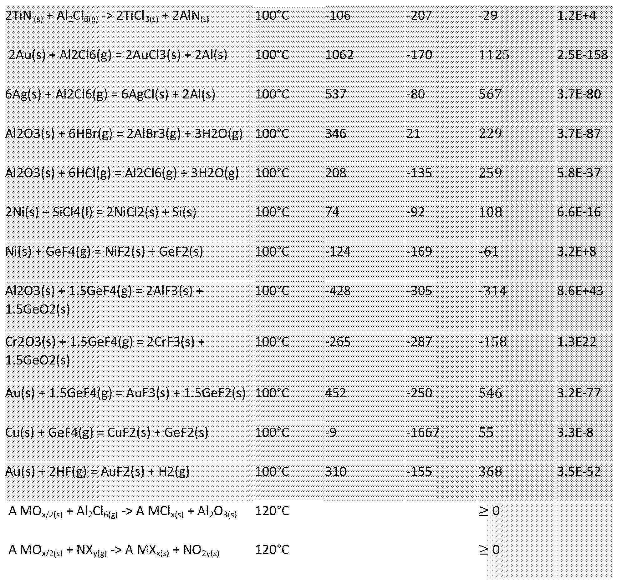
상기 표에서, A는 몰수이고, X는 할로겐화물이며, N은 임의의 금속이다. 예를 들어, NXy는 HfCl4 또는 WCl6일 수 있다.In the above table, A is mole number, X is halide, and N is any metal. For example, NX y can be HfCl 4 or WCl 6 .
표 1의 첫째 줄의 반응은 반도체 제조 설비에서 금속의 부식을 야기하지 않는데, 왜냐하면 반응의 자유 에너지가 양이기 때문이다. 그러나, 표 1의 두번째 줄의 반응은 부식을 야기할 수 있다. 스테인레스 강 반도체 제조 설비의 표면 산화물을 Cr2O3에서 Al2O3로 변화시킴으로써, 반응 구동력이 0이 되어간다. 다르게는, 표 1의 세번째 줄에서 보이는 바와 같이, 보호 산화물은 반응의 자유 에너지가 0 이상인 임의의 금속 산화물 MOx(여기에서, x는 화학량론적으로 적절한 값을 가짐)로부터 선택될 수 있다. 또한, 표 1의 네번째 줄에서 보이는 바와 같이, 일반적인 금속 할로겐화물 증기 NXy(예컨대, NF3)가 전달되는 경우, 보호 산화물은 반응의 자유 에너지가 0 이상인 금속 산화물 MOx로부터 선택될 수 있다. The reaction in the first row of Table 1 does not cause corrosion of the metal in the semiconductor manufacturing facility, because the free energy of the reaction is positive. However, the reaction in the second row of Table 1 can cause corrosion. By changing the surface oxide of the stainless steel semiconductor manufacturing facility from Cr 2 O 3 to Al 2 O 3 , the reaction driving force becomes zero. Alternatively, as shown in the third row of Table 1, the protective oxide can be selected from any metal oxide MO x (where x has a stoichiometrically appropriate value) with a free energy of reaction equal to or greater than zero. In addition, as shown in the fourth row of Table 1, when a typical metal halide vapor NX y (eg, NF 3 ) is delivered, the protective oxide may be selected from metal oxide MO x where the free energy of the reaction is zero or more.
본원의 보호 코팅을 이용하여 NF3, Al2Cl6, HfCl4, TiCl4, ZrCl4, WCl6, WCl5, VCl4, NbCl5, TaCl5 및 다른 금속 염화물 같은 부식성 시약에 대해 보호할 수 있다. 예를 들면, Al2O3를 이들 부식성 시약에 대한 보호 코팅 물질로서 사용할 수 있다. 플루오르, 염소, 브롬, 플루오르화수소, 염화수소, 브롬화수소, 이플루오르화제논, 삼플루오르화붕소, 사플루오르화규소, 사플루오르화게르마늄, 삼플루오르화인, 삼플루오르화비소, 삼염화붕소, 사염화규소, 오존 같은 기체 또는 증기로서 전달될 수 있는 반도체 물질은 부식 행태를 매개할 수 있고, Al2O3 코팅을 유용하게 사용하여 이러한 부식성 시약에 대해 보호 필름을 제공할 수 있다. 사염화티탄은 상당히 부식성이고 Y2O3에 대해 양의 ΔG를 갖는다.The protective coatings herein can be used to protect against corrosive reagents such as NF 3 , Al 2 Cl 6 , HfCl 4 , TiCl 4 , ZrCl 4 , WCl 6 , WCl 5 , VCl 4 , NbCl 5 , TaCl 5 and other metal chlorides. have. For example, Al 2 O 3 can be used as a protective coating material for these corrosive reagents. Fluorine, chlorine, bromine, hydrogen fluoride, hydrogen chloride, hydrogen bromide, non-fluorinated agent, boron trifluoride, silicon tetrafluoride, germanium tetrafluoride, phosphorus trifluoride, arsenic trifluoride, boron trichloride, silicon tetrachloride, ozone Semiconductor materials that can be delivered as the same gas or vapor can mediate corrosion behavior, and an Al 2 O 3 coating can be usefully used to provide a protective film against these corrosive reagents. Titanium tetrachloride is quite corrosive and has a positive ΔG for Y 2 O 3 .
구체적인 실시양태에서, Al2O3는 스테인레스 강 표면의 브롬화수소 노출에 대해 양의 ΔG를 갖는 보호 코팅 물질로서 사용된다. 다른 실시양태에서는, Al2O3가 스테인레스 강 표면의 염화수소 노출에 대해 양의 ΔG를 갖는 보호 코팅 물질로서 사용된다. 또 다른 실시양태에서는, 스테인레스 강 표면의 사염화규소 노출에 대해 양의 ΔG를 갖는 보호 코팅 물질로서 니켈이 사용된다. In a specific embodiment, Al 2 O 3 is used as a protective coating material with a positive ΔG for exposure to hydrogen bromide on stainless steel surfaces. In another embodiment, Al 2 O 3 is used as a protective coating material having a positive ΔG for exposure to hydrogen chloride on the stainless steel surface. In another embodiment, nickel is used as a protective coating material with a positive ΔG for exposure to silicon tetrachloride on the stainless steel surface.
추가적인 실시양태에서, 사플루오르화게르마늄에의 노출시 스테인레스 강 표면 상에서 양의 ΔG를 갖는 보호 코팅은 니켈, Al2O3 , Cr2O3, 금, 질화티탄(TiN) 같은 질화물, 유리 및 구리중 임의의 것을 포함할 수 있다. 사플루오르화게르마늄을 사용한 부동태화가 표면 Ni-F, Cr-F 및 Fe-F 물질(이는 니켈 또는 스테인레스 강 위에 놓이는 NiF2, CrF3 또는 FeF3 층으로서 생각될 수 있음)의 형성으로 인해 스테인레스 강에 대해 효과적이다.In a further embodiment, the protective coating with a positive ΔG on the stainless steel surface upon exposure to germanium tetrafluoride is nickel, Al 2 O 3 , Cr 2 O 3 , gold, nitrides such as titanium nitride (TiN), glass and copper It may include any of. Passivation with germanium tetrafluoride is due to the formation of surface Ni-F, Cr-F and Fe-F materials (which can be thought of as NiF 2 , CrF 3 or FeF 3 layers overlying nickel or stainless steel) stainless steel It is effective against.
다른 실시양태에서, 금은 스테인레스 강 표면의 플루오르화수소 노출에 대해 양의 ΔG를 갖는 보호 코팅 물질로서 사용된다.In another embodiment, gold is used as a protective coating material with a positive ΔG for exposure to hydrogen fluoride on a stainless steel surface.
다양한 실시양태에서, 스테인레스 강 및 탄소 강용 보호 코팅은 니켈 같은 금속 및 금속 합금을 포함한다. 다른 실시양태에서, 이러한 작업을 위한 보호 코팅은 상표면 테플론(Teflon)® 및 칼레즈(Kalrez)®로 시판되고 있는 물질의 보호 코팅을 비롯하여 폴리테트라플루오로에틸렌(PEFE) 또는 PTFE-유사 물질 같은 중합체 물질을 포함할 수 있다. 보호 코팅은 또한 하이드라이드 기체에의 노출에 의해 야기되는 스테인레스 강의 약화(embrittlement)를 피하기 위하여 사용될 수 있고, 이러한 보호 코팅은 알루미늄, 구리 또는 금 같은 물질로 제조될 수 있거나 또는 달리 이러한 물질을 포함할 수 있다. In various embodiments, protective coatings for stainless steel and carbon steel include metals and metal alloys, such as nickel. In other embodiments, protective coatings for such operations include polytetrafluoroethylene (PEFE) or PTFE-like materials, including protective coatings of materials commercially available under the trade names Teflon® and Kalez®. Polymer materials. Protective coatings can also be used to avoid stainless steel embrittlement caused by exposure to hydride gases, and these protective coatings can be made of materials such as aluminum, copper or gold, or otherwise include such materials Can.
표면 상에 보호 코팅이 제공되는 반응성 시약은 고체, 액체 및/또는 기체 형태일 수 있고, 혼합물 또는 하나 이상의 용매를 포함하는 용액일 수 있다. Reactive reagents that are provided with a protective coating on the surface can be in solid, liquid and/or gaseous form, and can be a mixture or a solution comprising one or more solvents.
더욱 일반적으로 ΔG와 관련하여, 압력 또는 온도 변화에 의해 10-4<K<10+4의 범위에서 안정성이 변동될 수 있으며, K>10+4인 경우에는 임의의 조건 하에서 부식이 거의 없어진다.More generally with respect to ΔG, stability can be varied in the range of 10 −4 <K<10 +4 by pressure or temperature change, and when K>10 +4 , corrosion is almost eliminated under any conditions.
ALD 또는 다른 기상 침착 기법에 의해 형성되는 본원의 조밀하고 핀홀이 없는 코팅은 천연 산화물 표면과는 구별된다. 천연 산화물 필름은 전형적으로 실온에서 또는 실온 근처에서 형성되고, 결정질이며, 이러한 천연 산화물 필름에 관련된 산화는 불완전할 수 있다. 이러한 천연 산화물 필름은 본원의 기상 침착 코팅, 예컨대 ALD 코팅보다 더 반응성이다. 본원의 조밀하고 두꺼우며 핀홀이 없는 기상 침착 코팅은 비정질이고 동형이다.The dense, pinhole-free coatings formed by ALD or other vapor deposition techniques are distinct from natural oxide surfaces. Natural oxide films are typically formed at or near room temperature, are crystalline, and the oxidation associated with these natural oxide films may be incomplete. These natural oxide films are more reactive than the vapor deposition coatings herein, such as ALD coatings. The dense, thick, pinhole-free vapor deposition coatings herein are amorphous and homogeneous.
본원에 따라 형성되는 스테인레스 강 상의 알루미나 코팅의 경우, Al2O3 코팅의 침착 전에 세정 또는 다른 전처리 단계를 이용할 수 있다. 예를 들면, 본원의 특정 실행에서 바람직하거나 유리할 수 있는 바와 같이 전해 연마 또는 감소 처리, 또는 이러한 처리의 조합을 이용할 수 있다. 임의의 다른 적합한 세정 또는 전처리 단계를 추가로 또는 선택적으로 사용할 수 있다. For alumina coatings on stainless steel formed according to the present application, cleaning or other pretreatment steps can be used prior to deposition of the Al 2 O 3 coating. For example, electropolishing or reducing treatment, or a combination of these treatments, may be used as may be desirable or advantageous in certain implementations herein. Any other suitable cleaning or pretreatment steps can be used additionally or alternatively.
삼염화알루미늄과 관련하여, AlCl3가 용매에, 또는 오일 또는 그리스(grease)에 용해되지 않지만, 예컨대 기화기가 가열될 때 기화를 위해 AlCl3 또는 다른 화학약품이 제공되는 고체 전달 기화기에서 오일 또는 그리스가 열 전달제로서 존재하여 용기로부터 분배되는 증기 스트림을 제공할 수 있음을 알게 된다. 예를 들어, 전달되어야 하는 AlCl3 또는 다른 화학약품을 고비점 불활성 오일 또는 그리스와 혼합하여, 고체 전달 용기에서 트레이 또는 다른 지지 표면 상으로 로딩되는 페이스트를 형성할 수 있다. 오일 또는 그리스는 열 전달제로서, 또한 작은 입자를 포획하고 이들 입자가 증기 유동에 연행되지 않게 방지하는 매질로서 작용한다. 이들 포획된 작은 입자는 기화됨으로써 열 전달제를 통과하고 궁극적으로는 기화기 용기에서 빠져나올 때까지 오일 또는 그리스에 보유된다. 이러한 방식으로, 오일 또는 그리스는 열 전달율을 개선할 수 있고, 기화기의 더 낮은 전달 온도가 달성될 수 있게 한다.With respect to aluminum trichloride, AlCl 3 is not soluble in a solvent, or in oil or grease, but oil or grease is present in a solid delivery vaporizer where, for example, AlCl 3 or other chemicals are provided for vaporization when the vaporizer is heated. It will be appreciated that it can exist as a heat transfer agent to provide a vapor stream distributed from the vessel. For example, AlCl 3 or other chemicals to be delivered can be mixed with a high boiling point inert oil or grease to form a paste that is loaded onto a tray or other support surface in a solid delivery vessel. Oil or grease acts as a heat transfer agent and also as a medium to trap small particles and prevent them from entraining the vapor flow. These trapped small particles vaporize and pass through the heat transfer agent and ultimately remain in the oil or grease until exiting the vaporizer vessel. In this way, oil or grease can improve the heat transfer rate and allow a lower transfer temperature of the vaporizer to be achieved.
이제, 도면을 참조하면, 도 1은 본원의 한 양태에 따른 반도체 웨이퍼 가공 도구(100)의 침착 로(102)의 개략도이다.Referring now to the drawings, FIG. 1 is a schematic diagram of a
로(102)는 도시된 바와 같이 내부 부피를 라이너(110) 내의 내부피(108) 및 라이너 외부의 외부 부피(106)로 분리하는 라이너(110)가 배치되는 가열된 내부 부피(104)를 한정한다. 웨이퍼가 로에서 공정 기체와 접촉할 수 있도록, 웨이퍼(114)가 장착된 웨이퍼 캐리어(112)가 라이너(110) 내의 내부피(108)에 위치한다.
도 1에 도시되어 있는 바와 같이, 제 1 공정 기체가 제 1 공정 기체 공급 라인(118)을 통해 제 1 공정 기체 공급원(116)으로부터 로의 내부피(108)로 공급될 수 있다. 유사한 방식으로, 제 2 공정 기체가 제 2 공정 기체 공급 라인(122)을 통해 제 2 공정 기체 공급원(120)으로부터 로의 내부피(108)로 공급될 수 있다. 제 1 및 제 2 공정 기체는 도구의 작업시 동시에 또는 연속적으로 로에 도입될 수 있다. 제 1 공정 기체는 예를 들어 웨이퍼 캐리어(112)의 웨이퍼 기판 상에 금속 성분을 증착시키기 위한 유기 금속 전구체를 포함할 수 있다. 제 2 공정 기체는 예를 들어 할로겐화물 세정 기체를 포함할 수 있다. 로의 내부피(108)에 도입된 기체는 라이너 내에서 상향 유동하고, 라이너(110)의 상부 개방 말단에서 흘러나갈 때 환상 외부 부피(106)에서 하향 유동한다. 이 기체는 이어 방출 라인(124)에서 로로부터 감쇠 단위장치(126)로 흘러나가고, 여기에서 로로부터의 유출 기체가 처리되어 그로부터 유해 성분이 제거되며, 처리된 기체는 배기 라인(128)에서 추가적인 처리 또는 다른 처분을 위해 방출된다. 감쇠 단위장치(126)는 습식 및/또는 건식 스크러버, 촉매에 의한 산화 장치, 또는 다른 적합한 감쇠 설비를 포함할 수 있다. As shown in FIG. 1, the first process gas may be supplied from the first
본원에 따라, 로 및 라이너 구성요소의 표면이 육염화이알루미늄(이는 로 안의 웨이퍼(114)가 의도된 목적에 모자라거나 또는 심지어 쓸모없게 되도록 함)으로부터의 화학적 공격에 저항하도록 이들 표면을 Al2O3 층으로 코팅한다.In accordance with the present application, these surfaces are Al 2 O so that the surfaces of the furnace and liner components are resistant to chemical attack from aluminum hexachloride (which causes the
도 2는 AlCl3를 기화시켜 Al2Cl6 증기를 형성시키기 위한 앰풀 형태의 고체 공급원 전달 기화기를 사용하는, Al2Cl6 증기를 사용하여 웨이퍼를 코팅하기 위한 본원의 다른 양태에 따른 침착 로 공정 시스템의 개략도이며, 이 때 상기 앰풀의 트레이 및 내표면은 Al2O3로 코팅되며 앰풀 하류의 밸브, 관 및 필터도 모두 Al2O3로 코팅된다. Figure 2 is a process at the deposition in accordance with another aspect of the present application for coating a wafer using, Al 2 Cl 6 steam using the Al 2 Cl 6 solid source of ampoule form for forming the vapor delivery vaporizer to vaporize the AlCl 3 A schematic diagram of the system, wherein the tray and inner surface of the ampoule are coated with Al 2 O 3 and the valves, tubes and filters downstream of the ampoule are also coated with Al 2 O 3 .
도시된 바와 같이, 앰풀에는 공급 용기("Ar")로부터의 아르곤 캐리어 기체가 공급되고, 캐리어 기체는 물질 유동 제어기("MFC")를 함유하는 캐리어 기체 공급 라인을 통해 앰풀로 유동된다. 앰풀에서는, 트레이 상에 지지되는 고체 AlCl3를 기화시키기 위하여 앰풀을 가열함으로써 생성되는 Al2Cl6 증기와 캐리어 기체가 접촉하고, 기화된 Al2Cl6는 웨이퍼(여기에는 Al2Cl6 증기로부터 알루미늄이 침착됨)를 함유하는 로로 유동된다. 도시된 바와 같이 침착을 위한 공동 반응물이 로로의 공동 반응물 공급 라인에 의해 로로 도입될 수 있다. 로를 통한 유체 유동은 펌프 및 압력 제어 밸브 어셈블리에 의해 제어되어, 로 내의 조건을 침착 작업에 적절하게 유지한다.As shown, the ampoule is supplied with argon carrier gas from a supply vessel (“Ar”), and the carrier gas is flowed into the ampoule through a carrier gas supply line containing a mass flow controller (“MFC”). In the ampoule, the Al 2 Cl 6 vapor produced by heating the ampoule to vaporize the solid AlCl 3 supported on the tray is in contact with the carrier gas, and the vaporized Al 2 Cl 6 is a wafer (here from the Al 2 Cl 6 vapor. Aluminum is deposited) into the furnace. As shown, the co-reactants for deposition can be introduced into the furnace by a co-reactant supply line to the furnace. Fluid flow through the furnace is controlled by a pump and pressure control valve assembly, keeping conditions within the furnace appropriate for deposition operations.
언급된 바와 같이, 앰풀의 트레이 및 내표면은 앰풀 하류의 모든 유동 회로 표면 및 구성요소에서와 마찬가지로 Al2O3로 코팅되어 육염화이알루미늄 증기에 의한 공격을 방지한다. 유동 회로 내의 필터는 금속 필터 요소를 갖는, 미국 매사추세츠주 빌러리카 소재의 엔테그리스, 인코포레이티드에서 상표명 웨이퍼가드(Wafergard)™ 및 가스켓가드(Gasketgard)™로 시판중인 유형의 것일 수 있다. As mentioned, the tray and inner surface of the ampoule are coated with Al 2 O 3 as in all flow circuit surfaces and components downstream of the ampoule to prevent attack by aluminum dichloride vapor. The filters in the flow circuit can be of the type commercially available under the trade names Wafergard™ and Gasketgard™ from Entegris, Inc. of Billerica, Mass., with metal filter elements.
도 3은 도 2의 침착 로 공정 시스템에 사용하기 적합한 유형의 기화기 앰풀의 일부가 절단된 사시도이다. 기화기 앰풀은 기체와 홀더에 의해 지지되는 물질로부터의 증기 사이의 접촉을 촉진하기 위하여 홀더를 갖는 용기(300)를 포함한다. 용기는 개별적인 지지 표면(311, 321, 331, 341, 351 및 361)을 한정하는 복수개의 홀더(310, 320, 330, 340, 350 및 360)를 갖는다. 용기는 표면(301)을 갖는 바닥 벽과 측벽(302)을 가져서, 용기(300)에서 대략 원통형 내부 영역을 한정하도록 하고, 용기(300) 상부 또는 그 근처에는 대략 원형 개구가 존재한다. 특정 실시양태에서 대략 원통형 내부 영역의 내경은 예를 들어 약 3인치 내지 약 6인치일 수 있다. 3 is a cut-away perspective view of a portion of a vaporizer ampoule of a type suitable for use in the deposition furnace process system of FIG. 2; The vaporizer ampoule includes a
용기(300)가 일체형 본체를 갖는 것으로 도 3에 도시되어 있으나, 용기는 별도의 부분으로부터 제조될 수 있다. 이 용기는 가공 설비로 전달하기 위하여 물질을 기화시키기 위한 앰풀을 제공한다. Although the
도 3에 도시되어 있는 바와 같이, 홀더(310)는 바닥 표면(301) 위에서 지지 표면(311)을 한정하도록 바닥 표면(301) 위에 위치할 수 있고, 홀더(320)는 지지 표면(311) 위에서 지지 표면(321)을 한정하도록 홀더(310) 위에 위치할 수 있고, 홀더(330)는 지지 표면(321) 위에서 지지 표면(331)을 한정하도록 홀더(320) 위에 위치할 수 있고, 홀더(340)는 지지 표면(331) 위에서 지지 표면(341)을 한정하도록 홀더(330) 위에 위치할 수 있고, 홀더(350)는 지지 표면(341) 위에서 지지 표면(351)을 한정하도록 홀더(340) 위에 위치할 수 있고, 홀더(360)는 지지 표면(351) 위에서 지지 표면(361)을 한정하도록 홀더(350) 위에 위치할 수 있다. 도 3에는 6개의 홀더(310, 320, 330, 340, 350 및 360)를 사용하는 것으로 도시되어 있으나, 임의의 적합한 수의 홀더를 기화기의 다양한 실시양태에서 사용할 수 있다. As shown in FIG. 3, the
도 3에 도시되어 있는 바와 같이, 대략 환형 지지체(304)가 용기(300)의 내부 영역에서 바닥 표면(301) 상에 위치하여, 홀더(310)를 바닥 표면(301) 위로 지지할 수 있다. 이어, 관(305)이 용기(300)의 내부 영역의 대략 중심 부위에서 홀더(360, 350, 340, 330, 320 및 310)의 개구를 통해 홀더(310)와 바닥 표면(301) 사이의 위치로 연장될 수 있다. As shown in FIG. 3, an approximately
일례로서, 도 3의 기화기는 관(305)의 말단에 배플 또는 확산기를 연결함으로써 변형되어 바닥 표면(301) 상에 지지되는 물질 위로의 직접적인 기체 유동을 도울 수 있다. 기체가 기화되어야 하는 물질을 지지하는 최저 홀더에서 또는 그 근처에서 도입되는 실시양태에서, 도입된 기체는 임의의 적합한 구조체를 이용하여 최저 홀더에 의해 지지되는 물질 위로 및/또는 물질을 통해 유동하도록 유도될 수 있다. As an example, the vaporizer of FIG. 3 can be modified by connecting a baffle or diffuser to the end of the
도 3에 도시된 바와 같이, 용기(300)는 용기(300) 꼭대기의 개구 둘레에 칼라를 가질 수 있고, 뚜껑(306)을 칼라 위에 위치시키고 예컨대 나사(307) 같은 나사를 사용하여 칼라에 고정시킬 수 있다. 임의적으로는 칼라 꼭대기의 개구 둘레에 홈을 한정하여, 용기(300)와 뚜껑(3060) 사이에 O-링(308)을 위치시키는데 도움을 줄 수 있다. O-링(308)은 예컨대 테플론®, 임의의 적합한 엘라스토머, 또는 예를 들어 스테인레스 강 같은 임의의 적합한 금속 등의 임의의 적합한 물질로 제조될 수 있다. 뚜껑(306)은 뚜껑(306)의 대략 중심 영역을 통해 개구를 한정할 수 있고, 이 개구를 통해 적어도 부분적으로는 관(305)에 의해 한정되는 통로 또는 입구가 용기(300)의 내부 영역 내로 연장될 수 있다. 뚜껑(306)이 용기(300)의 칼라에 고정될 때, 뚜껑(306)을 O-링(308) 쪽으로 가압하여 뚜껑(306)을 칼라 위에 밀봉시키는데 도움을 줄 수 있으며, 관(306) 둘레에서 칼라 쪽으로 가압하여 뚜껑(306)을 홀더(360, 350, 340, 330, 320 및 310) 쪽으로 가압하는데 도움을 줄 수 있다. 이어, 홀더(360, 350, 340, 330, 320 및 310)의 O-링을 압축시켜 홀더(360, 350, 340, 330, 320 및 310)를 서로에 대해 및/또는 관(305)에 대해 밀봉시키는데 도움을 줄 수 있다. 입구 연결장치(391)를 갖는 밸브(381)를 관(305)에 연결하여 용기(300) 내로의 기체의 도입을 조절하는데 도움을 줄 수 있다. 또한, 뚜껑(306)은 개구를 한정할 수 있고, 이를 통해 적어도 부분적으로는 관에 의해 한정되는 통로 또는 출구가 용기(300) 내로 연장될 수 있다. 출구 연결장치(392)를 갖는 밸브(382)를 관에 연결하여, 용기로부터의 기체 전달을 조절하는데 도움을 줄 수 있다. As shown in FIG. 3, the
도 3에 도시된 바와 같이, 대량 원형 프릿(370)을 상부 홀더(360) 위에 위치시켜, 뚜껑(306)을 통해 한정되는 출구를 통해 전달하기 전에 홀더(360)에 의해 지지되는 물질 위로 유도되는 기체 유동으로부터 고체 물질을 여과하는데 도움을 줄 수 있다. 프릿(370)은 프릿(370)의 대략 중심 영역을 통해 대략 원형 개구를 한정할 수 있고, 이를 통해 관(305)이 연장될 수 있다. 뚜껑(306)이 용기(300)에 고정될 때 임의의 적합한 구조체를 사용하여 임의의 적합한 방식으로 프릿(370)을 홀더(360) 위로 가압하여, 프릿(370)을 홀더(360) 위에 밀봉시키는데 도움을 줄 수 있다. 기화기는 프릿(370)에 부가하여 또는 이 대신에 용기(300)로부터의 기체 전달을 위한 통로 또는 출구에 위치하는 프릿 및/또는 홀더(310, 320, 330, 340, 350 및 360)중 하나 이상을 통한 하나 이상의 통로에 위치하는 하나 이상의 프릿을 포함할 수 있다. 기화기의 프릿(들)도 Al2O3로 코팅될 수 있다. 유사한 방식으로, 기화기의 임의의 다른 내부 구성요소를 Al2O3로 코팅하여, 기화기의 내부 부피의 모든 표면 및 구성요소가 Al2O3로 코팅되도록 할 수 있다. As shown in FIG. 3, a bulk
도 3의 기화기에서는, 밸브(381, 382) 사이에서 연결되는 관(395)에 의해 한정되는 우회 통로를 이용하여, 밸브(381, 382), 입구 연결장치(391) 및/또는 출구 연결장치(392)를 퍼지시키는데 도움을 줄 수 있다. 밸브(383)를 임의적으로 관(395)에 연결하여, 우회 통로를 통한 유체 유동을 조절하는데 도움을 줄 수 있다. 입구/출구 연결장치(397)을 임의적으로 이용하여, 용기(300)의 내부 영역에 대한 추가적인 입구/출구를 한정하는데 도움을 줌으로써, 내부 영역을 퍼지시키는데 도움을 줄 수 있다. In the carburetor of FIG. 3, the
도 4는 본원의 다른 양태에 따라 필터 요소에 유용하게 사용되는 유형의 다공성 금속 프릿의 표면의 15K 배율의 현미경 사진이다.4 is a micrograph of 15K magnification of the surface of a porous metal frit of the type useful for filter elements according to another aspect of the present application.
프릿의 높은 표면적은 유리하게는 ALD에 의해 코팅될 수 있으며, 이 때 금속 전구체 및 산화성 공동 반응물은 별도의 자기-한정 펄스에서 표면에 도달한다. 프릿을 Al2O3로 코팅하기 위하여, 트리메틸알루미늄 및 물 또는 O3/O2 혼합물의 교대하는 펄스를 사용할 수 있다. 구체적인 조건은 모든 표면이 코팅될 때까지 각 단계의 펄스 길이를 증가시킴으로써 실험적으로 결정될 수 있다. 100 내지 400℃의 침착 온도를 이용하여 구체적인 실시양태에서 유용한 필름을 침착시킬 수 있다. The high surface area of the frit can advantageously be coated by ALD, where the metal precursor and oxidative co-reactants reach the surface in separate self-limiting pulses. To coat the frit with Al 2 O 3 , alternating pulses of trimethylaluminum and water or an O 3 /O 2 mixture can be used. The specific conditions can be determined experimentally by increasing the pulse length of each step until all surfaces are coated. Films useful in specific embodiments can be deposited using a deposition temperature of 100 to 400°C.
본원의 폭 넓은 실행에 예컨대 AlCl3, 다른 AlR3(알킬) 화합물(이 때, R3은 유기 잔기임), 또는 다른 휘발성 Al 화합물 같은 다른 알루미늄 공급원을 사용할 수 있음을 알게 될 것이다. N2O, O2, 알콜, 퍼산화물 등과 같은 다른 산소 공급원을 또한 알루미늄 공급 시약과 함께 사용하여, 본원의 이러한 실행에서 Al2O3 또는 관련된 AlOx 물질을 침착시킬 수 있다.It will be appreciated that other aluminum sources such as AlCl 3 , other AlR 3 (alkyl) compounds (where R 3 is an organic moiety), or other volatile Al compounds may be used in the broad practice herein. Other oxygen sources such as N 2 O, O 2 , alcohols, peroxides, etc. can also be used in conjunction with aluminum feed reagents to deposit Al 2 O 3 or related AlO x materials in this practice herein.
본원의 특징 및 이점은 하기 실시예에 의해 더욱 충분히 기재되는데, 이들 실시예는 본원의 이해를 돕기 위한 예시적인 특성을 갖는다.The features and advantages herein are more fully described by the following examples, which have exemplary properties to aid understanding of the present application.
실시예 1Example 1
전해 연마된 316L 스테인레스 강 샘플을 이소프로판올로 세정하여 표면을 깨끗하게 만들었다. 2개의 샘플을 원자 층 침착(ALD)에 의해 Al2O3로 코팅하였다. 하나의 샘플은 트리메틸알루미늄/퍼지/물/퍼지의 100 ALD 사이클을 거쳤고, 다른 하나의 샘플은 동일한 ALD 공정의 1000 사이클을 거쳤다. 침착 온도는 150℃였다. 2개의 샘플은 코팅하지 않았다. 2개의 코팅된 샘플 및 하나의 코팅되지 않은 샘플을, 수분 또는 산소가 샘플 또는 AlCl3와 상호작용하지 않도록 방지하기 위하여 질소-퍼지되는 글로브박스에서, 고체 AlCl3 분말을 갖는 유리 앰풀 내로 로딩하였다. 이어, 유리 앰풀을 PTFE 캡으로 밀봉하였다. AlCl3 및 스테인레스 강 샘플을 갖는 앰풀을 10일동안 120℃로 가열하였다. 10일이 끝난 후, 앰풀을 냉각시키고 다시 글로브박스 내로 갖고 왔다. 이 불활성 환경 하에서 샘플을 AlCl3로부터 제거하였다. 샘플의 질량 증가는 0.4 내지 0.7mg(<0.15%)이었다. 모든 표면은 육안으로 깨끗해 보였다. 이어, 이들 세 개의 샘플 및 AlCl3에 노출되지 않은 추가의 샘플을 상부 표면에서 주사 전자 현미경(SEM)으로 시험하고, 이어 집속 이온 빔(FIB)에 의해 절단하여 표면 공격이 있는지의 여부를 결정하였다.The electropolished 316L stainless steel sample was cleaned with isopropanol to make the surface clean. The two samples were coated with Al 2 O 3 by atomic layer deposition (ALD). One sample went through 100 ALD cycles of trimethylaluminum/purge/water/purge, and the other sample went through 1000 cycles of the same ALD process. The deposition temperature was 150°C. Two samples were uncoated. Two coated samples and one uncoated sample were loaded into a glass ampoule with solid AlCl 3 powder in a nitrogen-purged glovebox to prevent moisture or oxygen from interacting with the sample or AlCl 3 . The glass ampoule was then sealed with a PTFE cap. The ampoule with AlCl 3 and stainless steel samples was heated to 120° C. for 10 days. After 10 days, the ampoule was cooled and brought back into the glovebox. Samples were removed from AlCl 3 under this inert environment. The mass gain of the sample was 0.4 to 0.7 mg (<0.15%). All surfaces were visually clean. These three samples and additional samples not exposed to AlCl 3 were then tested by scanning electron microscopy (SEM) on the top surface, and then cut by focused ion beam (FIB) to determine whether there was a surface attack. .
도 5는 AlCl3에 노출되지 않은 샘플의 표면 이미지를 도시한다. 이 샘플의 표면은 깨끗하고 스테인레스 강의 주요 원소, 즉 Fe, Cr 및 Ni를 보여준다.5 shows the surface image of a sample not exposed to AlCl 3 . The surface of this sample is clean and shows the major elements of stainless steel: Fe, Cr and Ni.
도 6은 AlCl3에 노출된 코팅되지 않은 샘플을 보여준다. 이 샘플 상에 상당한 표면 잔류물이 있고 스테인레스 강의 주성분에 Al 및 Cl이 부가되어 있음을 볼 수 있다.6 shows an uncoated sample exposed to AlCl 3 . It can be seen that there are significant surface residues on this sample and Al and Cl are added to the main components of the stainless steel.
도 7은 AlCl3에 노출되지 않은 샘플의 단면을 보여준다. 표면 공격이 없음이 명백하다.7 shows a cross-section of a sample not exposed to AlCl 3 . It is clear that there is no surface attack.
도 8은 AlCl3에 노출된 코팅되지 않은 샘플을 도시한다. Al- 및 Cl-함유 잔류물을 갖는 구역 아래에 0.1 내지 0.2마이크론의 표면 공격이 있었음이 명백하도록 표면에 대해 비교되는 선이 있다.8 shows an uncoated sample exposed to AlCl 3 . Below the zone with Al- and Cl-containing residues is a line that compares to the surface to make it clear that there was a surface attack of 0.1 to 0.2 microns.
도 9는 표면 코팅 없이 AlCl3에 노출된 샘플의 다른 구역을 보여준다. 처리되지 않은 스테인레스 강 표면에 천연 산화물이 존재한다. 이 구역에서는, 다수개의 피트가 명백히 보인다.9 shows another section of the sample exposed to AlCl 3 without surface coating. Natural oxides are present on the untreated stainless steel surface. In this area, multiple feet are clearly visible.
대조적으로, 도 10은 120℃에서 AlCl3에 노출되기 전에 TMA/H2O 100 사이클의 코팅을 가진 표면의 단면을 도시한다. 이 경우, 표면에 접착된 Al- 및 Cl-함유 잔류물이 여전히 존재하지만, 스테인레스 강 표면의 임의의 공격의 증거는 없다.In contrast, FIG. 10 shows a cross-section of a surface with a coating of TMA/H 2 O 100 cycles before exposure to AlCl 3 at 120°C. In this case, Al- and Cl-containing residues adhered to the surface still exist, but there is no evidence of any attack on the stainless steel surface.
마찬가지로, 도 11은 120℃에서 AlCl3에 노출되기 전에 TMA/H2O 1000 사이클의 코팅을 가진 표면의 단면을 도시한다. 이 경우, 표면에 접착된 Al- 및 Cl-함유 잔류물이 여전히 존재하지만, 스테인레스 강 표면의 임의의 공격의 증거는 없다.Likewise, FIG. 11 shows a cross-section of a surface with a coating of TMA/H 2 O 1000 cycles before exposure to AlCl 3 at 120°C. In this case, Al- and Cl-containing residues adhered to the surface still exist, but there is no evidence of any attack on the stainless steel surface.
실시예 2Example 2
구체적인 실험적 평가에서, 첫 번째 시험에서는 삼염화알루미늄(AlCl3)에 노출시켜, 또한 두 번째 시험에서는 오염화텅스텐(WCl5)에 노출시켜, 알루미나 코팅의 효능을 평가하였다.In a specific experimental evaluation, the efficacy of the alumina coating was evaluated by exposure to aluminum trichloride (AlCl 3 ) in the first test and tungsten contaminant (WCl 5 ) in the second test.
첫 번째 시험에서는, 전해 연마된 316L 스테인레스 강의 샘플 쿠폰을 Al2O3 470Å으로 코팅하거나 코팅하지 않았다. 각 유형의 샘플 하나를 고체 AlCl3가 든 2개의 용기중 하나에 위치시켰다. 두 용기 모두를 로딩하고 밀봉하고 N2 퍼지되는 글로브박스(0.1ppm 미만의 O2 및 H2O 수준) 내부에서 헬륨으로 3psig까지 가압하였다. 외부(outboard) He 누출 시험은 용기중 하나가 1E-6scc/s(이는 측정의 분석 한계임) 미만의 누출율을 가졌고 다른 하나의 용기가 2.5E-6scc/s의 누출율을 가진 것으로 결정하였다. 용기를 동일한 오븐에서 155℃로 9일간 가열하고 냉각시키고, 글로브박스에서 쿠폰을 제거하였다. 표 2는 다양한 쿠폰의 질량 변화를 보여준다.In the first test, sample coupons of electropolished 316L stainless steel were coated with or without Al 2 O 3 470 mm 3 . One sample of each type was placed in one of two containers with solid AlCl 3 . Both vessels were loaded, sealed and pressurized to 3 psig with helium inside an N 2 purged glovebox (O 2 and H 2 O levels below 0.1 ppm). The outboard He leak test determined that one of the containers had a leak rate of less than 1E-6scc/s (which is the analytical limit of measurement) and the other container had a leak rate of 2.5E-6scc/s. . The vessel was heated and cooled to 155°C for 9 days in the same oven, and the coupon was removed from the glove box. Table 2 shows the mass change of various coupons.
도 12는 155℃에서 AlCl3에 9일간 노출된 후 표 2의 샘플 쿠폰의 합성 사진이며, 여기에서 개별적인 쿠폰은 표 2에 기재된 것과 동일한 ID 번호로 확인된다.표 2로부터, 용기의 측정가능한 누출이 있는 경우에만 질량 변화가 칭량가능하다는 것이 명백하다. 이 부식성 노출에서, 표 2에 기재된 샘플의 질량 손실 및 도 12의 개별적인 샘플 쿠폰의 합성 사진은 코팅된 샘플 쿠폰(2)이 155℃에서 AlCl3에 9일간 노출된 후 코팅되지 않은 샘플 쿠폰(12)보다 상당히 더 우수한 상태로 있음을 보여준다. XRF에 의해 측정된 Al2O3 코팅 두께는 변화가 없었다.FIG. 12 is a composite photo of the sample coupon of Table 2 after 9 days of exposure to AlCl 3 at 155° C., where individual coupons are identified with the same ID number as described in Table 2. From Table 2, measurable leak of the container It is clear that the mass change is only measurable in this case. In this corrosive exposure, the mass loss of the samples listed in Table 2 and a composite photo of the individual sample coupons in FIG. 12 show that the
두 번째 시험에서는, 전해 연마된 316L 스테인레스 강의 샘플 쿠폰을 Al2O3 470Å 두께 코팅으로 코팅하거나 코팅하지 않았다. 샘플 쿠폰을 고체 WCl5가 든 용기에 넣었으며, 개별적인 용기에서 165℃, 180℃ 및 220℃의 온도 조건을 유지하였다. 모든 용기를 로딩하고 N2 퍼지되는 글로브박스(O2 및 H2O 수준은 0.1ppm 미만임) 내에서 밀봉하였다. 이어, 용기를 오븐에서 10일간 가열하고 냉각한 후, 샘플 쿠폰을 글로브박스에서 개별적인 용기로부터 제거하였다.In the second test, sample coupons of electropolished 316L stainless steel were coated with or without Al 2 O 3 470 mm thick coating. Sample coupons were placed in a container with solid WCl 5 and temperature conditions of 165°C, 180°C and 220°C were maintained in individual containers. All containers were loaded and sealed in an N 2 purged glovebox (O 2 and H 2 O levels less than 0.1 ppm). The vessel was then heated and cooled for 10 days in an oven, and then sample coupons were removed from the individual vessels in the glovebox.
x-선 형광(XRF) 분광 기법에 의해 두께를 측정하여, 최초 측정된 두께로부터 알루미나 코팅의 코팅 두께 면에서의 변화를 평가하였다. 표 3은 WCl5에 노출되기 전 및 후 Al2O3 두께의 XRF 측정치를 함유하며, 이 때 2개의 샘플 쿠폰은 이러한 노출시 165℃에서 10일간 유지시켰고, 2개의 샘플 쿠폰은 이러한 노출시 180℃에서 10일간 유지시켰으며, 1개의 샘플 쿠폰은 이러한 노출시 220℃에서 10일간 유지시켰다. 에칭 공정시 코팅 약 15 내지 30Å이 전형적으로 에칭되었다.The thickness was measured by x-ray fluorescence (XRF) spectroscopy technique to evaluate the change in coating thickness of the alumina coating from the first measured thickness. Table 3 contains XRF measurements of Al 2 O 3 thickness before and after exposure to WCl 5 , where two sample coupons were maintained at 165° C. for 10 days during this exposure, and two sample coupons were 180 during this exposure. The sample was maintained at 10°C for 10 days, and one sample coupon was maintained at 220°C for 10 days upon exposure. During the etching process, about 15 to 30
도 13은 220℃에서 10일간 WCl5에 노출된 샘플의 상부-하향 주사 전자 현미경(SEM) 현미경사진이고, 도 14는 이러한 샘플에서 코팅의 가장자리의 집속 이온 빔(FIB) 단면이다. 이 두 번째 시험에서 코팅된 샘플 및 코팅되지 않은 샘플은 육안에 의해 또는 SEM 시험에 의해 또는 중량 변화에 의해 부식의 징후를 보이지 않았다. 그러나, 더 높은 온도에서는 상당량의 Al2O3 코팅이 제거되었다. 165℃에서의 두 샘플은 모두 세정 공정에 일치되는 양으로 에칭되었다. 180℃에서의 샘플중 하나는 세정에 상응하는 27Å을 상실하였으나, 다른 하나의 샘플은 약 66Å의 두께를 상실하였고 이는 세정시 상실보다 상당히 더 높은 값이다. 220℃에서는, 알루미나 코팅이 일부 구역(더 밝은 구역)에서는 제거되고 다른 구역(더 어두운 구역)에서는 완전하게 유지되는 도 13에 도시된 바와 같이 코팅의 약 60%가 제거되었다. 도 14에서, 현미경사진은 오른쪽에 완전하게 유지되는 코팅을 보여주고 코팅된 구역의 가장자리는 화살표로 표시된다.13 is a top-down scanning electron microscope (SEM) micrograph of a sample exposed to WCl 5 for 10 days at 220° C., and FIG. 14 is a focused ion beam (FIB) cross-section of the edge of the coating in this sample. The coated and uncoated samples in this second test showed no signs of corrosion by the naked eye or by SEM testing or by weight change. However, at higher temperatures, a significant amount of Al 2 O 3 coating was removed. Both samples at 165°C were etched in an amount consistent with the cleaning process. One of the samples at 180° C. lost 27
본원이 예시적으로 반도체 제조 설비에 관한 것이긴 하지만, 공정 설비에서의 표면이, 작업시 산화물과 반응하여 이러한 설비를 이용하여 제조되는 제품 및 이러한 설비를 이용하여 수행되는 공정에 유해한 반응 생성물을 생성시키는 증기 상 성분에 의해 공격을 받기 쉬운, 평면 패널 디스플레이, 태양 전지, 태양광 패널 등과 같은 다른 제품을 제조하기 위한 다른 기체 가공 장치에, 본원의 보호 코팅 해결책이 마찬가지로 적용될 수 있음을 알게 될 것이다. Although the present application is illustratively related to a semiconductor manufacturing facility, a surface in a processing facility reacts with oxides during work to produce products manufactured using such equipment and reaction products harmful to processes performed using such equipment. It will be appreciated that the protective coating solution herein can likewise be applied to other gas processing devices for manufacturing other products, such as flat panel displays, solar cells, solar panels, etc., which are susceptible to attack by vapor phase components.
아래에는 박막 원자 층 침착 코팅에 관련된 본원의 추가적인 양태가 기재된다.Below, additional aspects of the present application relating to thin film atomic layer deposition coatings are described.
다양한 조성물 및 방법이 기재되었으나, 본 발명은 기재된 특정한 분자, 조성물, 디자인, 방법 또는 프로토콜로 한정되지 않음(왜냐하면 이들은 변할 수 있기 때문에)을 알아야 한다. 또한, 본원에 사용되는 용어는 특정 버전 또는 실시양태를 기재하는 목적만을 위한 것이며 본 발명의 영역을 한정하고자 하지 않음을 알아야 한다.While various compositions and methods have been described, it should be understood that the invention is not limited to the particular molecules, compositions, designs, methods or protocols described (because they can vary). In addition, it should be understood that the terminology used herein is for the purpose of describing specific versions or embodiments only and is not intended to limit the scope of the invention.
본원에 사용되는 단수형은 문맥상 명백하게 달리 해석되지 않는 한 복수 인용물을 포함한다. 그러므로, 예를 들어 "층"을 인용하는 것은 당 업자에게 공지되어 있는 하나 이상의 층 및 그의 등가물 등을 인용하는 것이다. 달리 한정되지 않는 한, 본원에 사용되는 모든 기술적 용어 및 과학적 용어는 당 업자가 통상적으로 아는 것과 동일한 의미를 갖는다.As used herein, the singular form includes the plural citation unless the context clearly indicates otherwise. Thus, for example, citing “layer” refers to one or more layers known to those skilled in the art and equivalents thereof. Unless otherwise limited, all technical and scientific terms used herein have the same meaning as commonly understood by one of ordinary skill in the art.
본원에 기재된 것과 유사하거나 본원에 기재된 것의 등가물인 방법 및 물질을, 본원의 실시양태의 실행 또는 시험에 사용할 수 있다. 본원에 언급되는 모든 간행물은 본원에 참고로 인용된다. 본원에서 특허청구되는 발명이 종래의 발명 때문에 이러한 간행물에 선행하는 것으로 인정되지 않는다고 간주되어야 하는 것은 아니다. "임의적임" 또는 "임의적으로"는 후속 기재되는 사건 또는 상황이 일어날 수 있거나 일어나지 않을 수 있고 이 기재가 사건이 일어나는 경우 및 일어나지 않는 경우를 포함함을 의미한다. 본원의 모든 수치 값은 명시적으로 표시되든 표시되지 않든 상관없이 용어 "약"으로 수식될 수 있다. 용어 "약"은 일반적으로 당 업자가 인용된 값에 상응하는 것으로(즉, 유사한 기능 또는 결과를 갖는 것으로) 생각하는 수치의 범위를 가리킨다. 일부 실시양태에서, 용어 "약"은 언급된 값의 ±10%를 가리키고, 다른 실시양태에서 용어 "약"은 언급된 값의 ±2%를 가리킨다. 조성물 및 방법이 다양한 성분 및 단계를 "포함하는"이라는 용어로 기재되지만, 이러한 용어는 본질적으로 닫힌 또는 닫힌 일원의 군을 한정하는 것으로 해석되어서는 안된다.Methods and materials similar to those described herein or equivalent to those described herein can be used in the practice or testing of embodiments herein. All publications mentioned herein are incorporated herein by reference. It is not to be considered that the invention claimed herein is not admitted to precede this publication because of the prior invention. "Random" or "optionally" means that the event or situation that is subsequently described may or may not occur, and that the description includes when and when the event occurs. All numerical values herein can be modified with the term "about", whether explicitly indicated or not. The term “about” generally refers to a range of values that a person considers to correspond to the recited value (ie, to have a similar function or result). In some embodiments, the term “about” refers to ±10% of the stated value, and in other embodiments the term “about” refers to ±2% of the stated value. Although the compositions and methods are described in terms of “comprising” various components and steps, these terms should not be construed as limiting the group of essentially closed or closed members.
본원에 사용되는 용어 "필름"은 1000㎛ 미만, 예를 들어 이 값으로부터 원자 단일 층 두께 값까지의 두께를 갖는 침착된 물질의 층을 가리킨다. 다양한 실시양태에서, 본 발명의 실행시 침착된 물질 층의 필름 두께는 관련되는 특정 용도에 따라 예를 들어 100, 50, 20, 10 또는 1㎛ 미만일 수 있거나, 또는 다양한 박막 체계에서는 200, 100, 50, 20 또는 10nm 미만일 수 있다. 본원에 사용되는 용어 "박막"은 1㎛ 미만의 두께를 갖는 물질의 층을 의미한다.The term “film” as used herein refers to a layer of deposited material having a thickness of less than 1000 μm, for example from this value to the atomic single layer thickness value. In various embodiments, the film thickness of a layer of material deposited in the practice of the present invention may be less than, for example, 100, 50, 20, 10 or 1 μm, or 200, 100, in various thin film systems, depending on the particular application involved. It may be less than 50, 20 or 10 nm. The term "thin film" as used herein means a layer of material having a thickness of less than 1 μm.
본원이 하나 이상의 실행과 관련하여 본원에 기재되었으나, 당 업자는 본원을 읽고 이해한 바에 기초하여 상응하는 변화 및 변형을 이끌어내게 된다. 본원은 이러한 변화 및 변형을 모두 포함한다. 또한, 본원의 특정 특징 또는 양태가 몇 가지 실행중 하나만과 관련하여 개시되었으나, 이러한 특징 또는 양태는 임의의 소정 또는 특정 용도에 요구되고 유리할 수 있는 바와 같이 다른 실행의 하나 이상의 다른 특징 또는 양태와 결합될 수 있다. 뿐만 아니라, 용어 "포함하다", "갖는", "가지다", "갖고" 또는 이들의 변형 용어가 본원에 사용되는 한도내에서, 이 용어는 용어 "포함하는"과 유사한 방식으로 포함하고자 한다. 또한, 용어 "예시적인"은 최선이라기보다는 일례를 의미할 뿐이다. 또한, 본원에 묘사된 특징, 층 및/또는 요소는 간단하게 하고 용이하게 이해하도록 하기 위하여 서로에 대한 특정 치수 및/또는 배향으로 예시 및/또는 교시되고, 실제 치수 및/또는 배향은 본원에 도시되고/되거나 교시된 것과는 실질적으로 상이할 수 있음을 또한 알아야 한다.Although this application has been described herein in connection with one or more implementations, those skilled in the art will elicit corresponding changes and modifications based on reading and understanding the application. This application includes all such changes and modifications. In addition, while certain features or aspects herein have been disclosed in connection with only one of several implementations, these features or aspects are combined with one or more other features or aspects of other implementations as may be required and advantageous for any given or specific use. Can be. In addition, to the extent that the terms “include”, “having”, “having”, “having” or variations thereof are used herein, the term is intended to be included in a manner similar to the term “comprising”. Also, the term “exemplary” is meant to be an example rather than the best. Also, features, layers, and/or elements depicted herein are illustrated and/or taught in specific dimensions and/or orientations relative to each other for simplicity and ease of understanding, and actual dimensions and/or orientations are shown herein. It should also be appreciated that it may and/or may be substantially different from what is taught.
그러므로, 본원은 그의 특징, 양태 또는 실시양태와 관련하여 본원에 다양하게 기재된 바와 같이 특정 실행에서 이러한 특징, 양태 및 실시양태중 일부 또는 모두를 포함하거나, 이들로 이루어지거나, 본질적으로 이들로 이루어질 수 있으며, 이의 요소 및 구성요소는 본원의 다양한 다른 실행을 구성하도록 합쳐진다. 따라서 본원은 다양하게 치환 및 조합되는 이러한 특징, 양태 및 실시양태, 또는 이들중 선택된 하나 또는 여럿이 본원의 영역 내에 속하는 것으로 고려한다. 또한, 본원은 본원의 다른 실시양태와 관련하여 본원에 개시된 임의의 하나 이상의 특정 특징, 양태 또는 요소를 배제함으로써 한정될 수 있는 실시양태를 고려한다.Therefore, the present application may include, consist of, or consist essentially of, some or all of these features, aspects and embodiments in a particular implementation as variously described herein in connection with its features, aspects or embodiments, , Elements and components thereof are incorporated to constitute various other implementations herein. Accordingly, the present application contemplates that various features and embodiments, or one or more of these characteristics, aspects and embodiments, which are substituted and combined, fall within the scope of the present application. In addition, the present application contemplates embodiments that may be defined by excluding any one or more specific features, aspects or elements disclosed herein in connection with other embodiments herein.
본원의 한 양태에 따라, 하나 이상의 층으로 구성되는 박막 코팅이 제공되며, 이 때 하나 이상의 층은 원자 층 침착에 의해 침착된다.According to one aspect of the present application, a thin film coating consisting of one or more layers is provided, wherein the one or more layers are deposited by atomic layer deposition.
본원의 양태에 따라, 하기가 제공된다:According to aspects herein, the following are provided:
- 1Å보다 큰 필름 두께, 일부 용도에서는 10,000Å보다 큰 필름 두께를 갖는 ALD 코팅.-ALD coating with a film thickness greater than 1 mm2 and in some applications greater than 10,000 mm2.
- 매우 조밀하고 핀홀이 없는 무결함 층을 제공하는 ALD 코팅.-ALD coating providing a very dense, pinhole-free, flawless layer.
- 다수개의 부품 상에 침착시키고자 하는(그러나 Si 웨이퍼 상에서 제조되는 실제 IC 장치(트랜지스터)의 경우에는 직접은 아님) 박막 코팅.-Thin film coating that is intended to be deposited on multiple parts (but not directly in the case of actual IC devices (transistors) manufactured on Si wafers).
- ALD 코팅은 알루미나(Al2O3), 이트리아(Y2O3), 지르코니아(ZrO2), 티타니아(TiO2) 등과 같은 절연 금속 산화물, 및 백금, 니오브 또는 니켈 같은 금속으로 이루어질 수 있다. -ALD coating can be made of insulating metal oxides such as alumina (Al 2 O 3 ), yttria (Y 2 O 3 ), zirconia (ZrO 2 ), titania (TiO 2 ), and metals such as platinum, niobium or nickel .
- ALD 코팅은 RT(실온) 내지 400℃에서 침착될 수 있다.-ALD coating can be deposited at RT (room temperature) to 400°C.
- ALD 코팅은 예컨대 1μ 두께의 알루미나 층 같은 한정된 화학량론을 갖는 단일 필름, 또는 예를 들어 {0.25μ 티타니아+0.5μ 알루미나+0.25μ 지르코니아} 같은 수 개의 층, 또는 예를 들어 {1개의 원자 층 티타니아+2개의 원자 층 알루미나}×n(여기에서, n은 1 내지 10,000임) 같은 진정한 다층 구조체, 또는 이들의 조합일 수 있다. -ALD coating is a single film with a limited stoichiometry, for example a 1 μ thick alumina layer, or several layers, for example {0.25 μ titania+0.5 μ alumina+0.25 μ zirconia}, or for example {1 atomic layer Titania+2 atomic layer alumina}×n (where n is 1 to 10,000), or a multi-layer structure, or a combination thereof.
- ALD 층이 PE-CVD, PVD, 스핀-온 또는 졸-겔 침착, 대기 플라즈마 침착 등과 같은 상이한 침착 기법에 의해 침착된 다른 층과 조합된 박막 코팅.-ALD layer thin film coating combined with other layers deposited by different deposition techniques such as PE-CVD, PVD, spin-on or sol-gel deposition, atmospheric plasma deposition, etc.
- 1μ 내지 100μ의 총 필름 두께.-Total film thickness from 1 μ to 100 μ.
- 전체 적층체의 ALD 코팅 두께 부분이 2μ 이하임(2μ은 하나 이상의 개별적인 층임).-The ALD coating thickness portion of the entire laminate is 2 μ or less (2 μ is one or more individual layers).
- 알루미나, 옥시질화알루미늄, 이트리아, 이트리아-알루미나 믹스, 산화규소, 옥시질화규소, 전이금속 산화물, 전이금속 옥시-질화물, 희토류 금속 산화물, 희토류 금속 옥시-질화물 같은 산화물의 군으로부터 선택되는 다른 코팅 물질.-Other coatings selected from the group of oxides such as alumina, aluminum oxynitride, yttria, yttria-alumina mix, silicon oxide, silicon oxynitride, transition metal oxide, transition metal oxy-nitride, rare earth metal oxide, rare earth metal oxy-nitride matter.
- ALD 코팅을 패턴화하는 능력.-The ability to pattern ALD coatings.
- 방법 1: 부품을 균일하게 코팅한 다음 마스크를 통해 원치 않는 물질을 에칭함(기계적, 예를 들어 비드 블라스트, 물리적, 예를 들어 플라즈마 이온, 또는 화학적, 예컨대 플라즈마 또는 습식 에칭에 의해 에칭해낼 수 있음).-Method 1: Uniformly coat the part and then etch unwanted material through the mask (can be etched mechanically, for example by bead blast, physical, for example plasma ion, or chemically, for example plasma or wet etching has exist).
- 방법 2: 원치 않는 구역을 마스킹하고, ALD 코팅한 다음, 마스킹된 구역을 제거함. 마스크는 밀봉된 시트, 또는 고정 비품 또는 포토레지스트(박리 기법)일 수 있다.-Method 2: Mask the unwanted area, ALD coated and then remove the masked area. The mask can be a sealed sheet, or a fixture or photoresist (peeling technique).
- 방법 3: ALD 필름 성장을 차단하는 표면 종결 층으로 기판 상에 패턴을 생성시킴. 예를 들어, H2O 및 TMA(트리메틸알루미늄)에 대한 점착 계수가 "0"인 표면 종결 층을 사용할 수 있다. 본원에 사용되는 표면 종결 층은 자가-한정 층, 예를 들어 자가-한정 ALD 층이다. 본원에 사용되는 점착 계수는 표면에 흡착되거나 "들러붙는" 흡착제 원자(또는 분자)의 수 대 동일한 기간 동안 그 표면 상에 충돌하는 아이템의 총 수의 비이다.-Method 3: Create a pattern on the substrate with a surface termination layer that blocks ALD film growth. For example, a surface termination layer having an adhesion coefficient of “0” for H 2 O and TMA (trimethylaluminum) can be used. The surface termination layer as used herein is a self-limiting layer, for example a self-limiting ALD layer. The coefficient of adhesion as used herein is the ratio of the number of adsorbent atoms (or molecules) adsorbed or "sticking" to a surface to the total number of items impinging on that surface for the same period of time.
본원의 양태에 따라, 하기 용도가 제공된다:According to aspects herein, the following uses are provided:
용도:purpose:
- 부품의 조밀하고 핀홀 없는 무결함 전기 절연.-Compact, pinhole-free, fault-free electrical insulation of parts.
- 높은 종횡비의 특징부를 갖는 부품을 코팅하는 능력. 예: (1) 깊은 구멍, 채널 및 3차원 특징부가 있는 부품, (2) 나사 및 너트 같은 장비, (3) 다공성 막, 필터, 3차원 망상조직 구조체, (4) 연속 공극 매트릭스를 갖는 구조체.-Ability to coat parts with high aspect ratio features. Examples: (1) deep holes, parts with channels and three-dimensional features, (2) equipment such as screws and nuts, (3) porous membranes, filters, three-dimensional network structures, and (4) structures with a continuous pore matrix.
- 전기 절연 층: 높은 유전성 파괴 강도 및 높은 전기 저항(낮은 누전). 이는 ALD Al2O3로 달성됨. 티타니아-알루미나-지르코니아(TAZ)의 다층을 사용하면 전기 절연체 성능을 추가로 개선시킨다. 다양한 다층 구성이 있다:-Electrical insulation layer: high dielectric breakdown strength and high electrical resistance (low leakage). This was achieved with ALD Al 2 O 3 . The use of titania-alumina-zirconia (TAZ) multilayers further improves electrical insulator performance. There are various multilayer configurations:
Xnm TiO2 + Ynm Al2O3 + Znm ZrO2 Xnm TiO 2 + Ynm Al 2 O 3 + Znm ZrO 2
[Unm TiO2 + Vnm Al2O3 + Wnm ZrO2T] × n[Unm TiO 2 + Vnm Al 2 O 3 + Wnm ZrO 2 T] × n
Xnm TiO2 + [Vnm Al2O3 + Wnm ZrO2T] × m 등.Xnm TiO 2 + [Vnm Al 2 O 3 + Wnm ZrO 2 T] × m etc.
여기에서, X, Y, Z, U, V 및 W는 각각 0.02nm 내지 500nm일 수 있고, n 및 m은 각각 2 내지 2000일 수 있다. Here, X, Y, Z, U, V, and W may be 0.02 nm to 500 nm, respectively, and n and m may be 2 to 2000, respectively.
- 내약품성 및 에칭 저항성 코팅: ALD 층은 알루미나, 이트리아, 세리아 등일 수 있다. 전체 에칭 저항성 코팅은 (1) ALD 층으로만 구성될 수 있고, (2) PVD, CVD 및 ALD의 조합으로 이루어질 수 있으며, (3) ALD가 이후 더욱 상세하게 논의되는 바와 같이 상부 코팅되고 밀봉제 층으로서의 역할을 할 수 있으며, (4) ALD가 하부 층이어서 강건항 토대를 제공할 수 있고, (5) ALD가 CVD 코팅 층 및/또는 PVD 코팅 층 사이에 끼일 수 있다.-Chemical resistant and etching resistant coating: ALD layer can be alumina, yttria, ceria, etc. The entire etch resistant coating can consist of (1) only an ALD layer, (2) a combination of PVD, CVD and ALD, and (3) an ALD top coated and sealant as discussed in more detail below. It can serve as a layer, (4) ALD can be a lower layer to provide a strong term foundation, and (5) ALD can be sandwiched between a CVD coated layer and/or a PVD coated layer.
- ALD 코팅은 고급(advanced) 배터리, 기체 필터, 액체 필터, 전기-도금 도구 구성요소, 플라즈마-습윤되는 구성요소(플루오르 및 다른 할로겐 공격에 대해 보호하기 위하여) 등과 같은 용도에 내약품성을 제공할 수 있다.-ALD coatings provide chemical resistance to applications such as advanced batteries, gas filters, liquid filters, electro-plating tool components, plasma-wetting components (to protect against fluorine and other halogen attacks), etc. Can.
- ALD 코팅은 내식성 코팅으로서의 역할을 할 수 있다. -ALD coating can serve as a corrosion-resistant coating.
- 확산 차단 층; 조밀하고 핀홀이 없는 동형 ALD 층은 탁월한 미량 금속 확산 차단 특징을 제공한다.-Diffusion barrier layer; The dense, pinhole-free homogeneous ALD layer provides excellent trace metal diffusion barrier properties.
- ALD 층은 아래에 놓이는 기판(유리, 석영, 알루미늄, 애노드화된 알루미늄, 알루미나, 스테인레스 강, 규소, SiOx, AlON 등)과 위에 놓이는 코팅 층(PVD 이트리아, PVD AlON, PVD Al2O3, CVD SiOx, CVD SiOxNy, CVD Al2O3, CVD AlOxNy, DLC, Si, SiC 등) 사이의 접착 층으로서의 역할을 할 수 있다. -ALD layer is the underlying substrate (glass, quartz, aluminum, anodized aluminum, alumina, stainless steel, silicon, SiO x , AlON, etc.) and the underlying coating layer (PVD yttria, PVD AlON, PVD Al 2 O 3 , CVD SiO x , CVD SiO x N y , CVD Al 2 O 3 , CVD AlO x N y , DLC, Si, SiC, etc.).
본원의 다른 양태에 따라, ALD-침착된 표면 밀봉 층을 코팅에 사용한다. ALD(원자 층 침착)는 둘 이상의 교대하는 전구체의 화학적 흡착을 이용하여 매우 조밀하고 거의 완벽하게 배열된(물리적으로, 또한 화학량론적으로) 박막을 형성하는 확립된 기법이다. 이 기법은 정밀하게 제어되는 필름 성장을 허용하고, 거의 100% 동형이며, 매우 높은 종횡비의 특징부 내를 비롯하여 전구체 기체가 도달할 수 있는 임의의 표면 위치에서 필름을 성장시킨다. 이와 관련하여, ALD-침착되는 밀봉 코팅을 하기 용도에 사용할 수 있다:According to another aspect of the present application, an ALD-deposited surface sealing layer is used for coating. ALD (Atomic Layer Deposition) is an established technique for forming very dense and almost perfectly aligned (physically and stoichiometrically) thin films using chemical adsorption of two or more alternating precursors. This technique allows for precisely controlled film growth, and grows the film at any surface location that the precursor gas can reach, including within features of nearly 100% homogeneous, very high aspect ratio. In this regard, ALD-deposited sealing coatings can be used for the following applications:
(1) 기존 표면 위를 코팅 및 밀봉하여, 이 표면/부품의 향상되고 탁월한 특성을 제공함, (1) Coating and sealing on the existing surface, providing improved and excellent properties of this surface/part,
(2) CVD, PVD, 분무 또는 다른 코팅 위에 ALD 밀봉 코팅을 도포하여, 코팅의 결함에 대한 밀봉제를 제공함, 예를 들어(2) Applying an ALD sealing coating over CVD, PVD, spraying or other coatings to provide a sealant for defects in the coating, e.g.
(i) 코팅 표면 근처의 임의의 균열을 채우고, 따라서 부식성의 에칭 환경에 불투과성인 표면을 제공함, (i) filling any cracks near the coating surface, thus providing a surface impermeable to a corrosive etching environment,
(ii) 임의의 거대 공극, 코팅 결함, 관입부(intrusion) 등을 채우고 밀봉하여, 기체 및 액체에 대해 불투과성이고 제어되는 매끈한 동형 밀봉 층으로 종결되는 코팅 표면 층을 제공함,(ii) filling and sealing any macro voids, coating defects, intrusions, etc., to provide a coating surface layer that is impermeable to gases and liquids and terminates with a controlled smooth homogeneous sealing layer,
(iii) 코팅의 표면 조도 및 전체적인 표면적을 감소시키고, 따라서 부식성 환경에서 최소한으로만 공격받는 매끈하고 조밀한 표면 층을 제공함,(iii) reducing the surface roughness and overall surface area of the coating, thus providing a smooth and dense surface layer that is minimally attacked in corrosive environments,
(iv) 상부 코팅으로 조밀하고 매끈하게 밀봉된 표면을 제공함으로써 입자 생성을 최소화하고, 경도, 인성 및 내긁힘성을 개선함.(iv) Minimize particle generation and improve hardness, toughness and scratch resistance by providing a dense, smoothly sealed surface with a top coating.
본원의 다양한 양태에서, ALD 밀봉제는 (a) 개선된 에칭 저항성 및 내식성, 및/또는 (b) 감소된 마찰, 마모 및 개선된 기계적 내마모성을 필요로 하는 부품 및 표면에 도포될 수 있다. In various embodiments herein, the ALD sealant can be applied to parts and surfaces that require (a) improved etch resistance and corrosion resistance, and/or (b) reduced friction, wear and improved mechanical wear resistance.
동시에 ALD 밀봉 층은 확산 차단벽으로서의 역할도 할 수 있으며, 이는 표면 전기 특성 뿐만 아니라 친수성 및 소수성 같은 표면 종결 특성을 제어하는 능력을 갖는다.At the same time, the ALD sealing layer can also serve as a diffusion barrier, which has the ability to control surface electrical properties as well as surface termination properties such as hydrophilicity and hydrophobicity.
본원의 추가적인 양태는 알루미나, 이트리아 또는 이 유형의 다른 코팅 같은 내약품성 코팅을 갖는 섬유상 금속 막을 이용하는 ALD 기법의 사용을 포함한다. ALD 기법은 기체가 섬유상 막 위에서 다공성 필터 및 코팅을 침투하여 부식성 기체에 대한 저항성을 제공하도록 할 수 있다.Additional aspects herein include the use of ALD techniques using fibrous metal films with chemically resistant coatings such as alumina, yttria or other coatings of this type. The ALD technique allows the gas to penetrate the porous filter and coating over the fibrous membrane to provide resistance to corrosive gases.
본원의 이 양태는 작은 미크론 크기의 개구를 침투하고 섬유 상에서 균일하게 코팅할 수 있는 침착 기체에 기초한 기법을 제공한다.This aspect of the present application provides a technique based on a deposition gas that can penetrate small micron-sized openings and uniformly coat on the fibers.
본원의 이 양태는 미국 매사추세츠주 빌러리카 소재의 엔테그리스, 인코포레이티드에서 제조된 4μ Ni-계 기체 필터 상에 알루미나 코팅을 침착시킴으로써 입증되었다.This aspect of the present application was demonstrated by depositing an alumina coating on a 4μ Ni-based gas filter manufactured by Entegris, Inc. of Billerica, Massachusetts.
본원의 ALD 기법은 1) 필터의 미크론 크기의 공극 같은 작은 특징부 내로의 코팅 침투(완벽한 도포율을 보장함), 2) 섬유의 밀폐성 밀봉(따라서, 필터 막을 보호함), 3) 이 기법을 이용하여 다양하고 상이한 코팅을 침착시킬 수 있는 것과 같은 다양한 이점을 제공한다.The ALD technique herein includes 1) coating penetration into small features, such as micron-sized pores of the filter (to ensure a perfect coverage), 2) sealing sealing of the fibers (and thus protecting the filter membrane), 3) this technique It provides various advantages such as being able to deposit various and different coatings.
본원은 또한 코팅되는 기판 제품 또는 설비의 가공 특징을 개선하기 위한 ALD 코팅의 용도를 고려한다. 예를 들어, 기판 제품의 어닐링 동안 발생될 수 있는 블리스터링(blistering) 또는 다른 바람직하지 못한 현상(다층 필름 제품의 층사이의 열 팽창 계수의 미스매치 때문에)에 대항하기 위해 ALD 필름을 사용할 수 있다. 그러므로, ALD 필름을 다층 필름 구조체에 사용하여, 이러한 물질 특성 차이를 경감시키거나 또는 최종 생성물 제품의 전기적, 화학적, 열적 및 다른 성능 특성을 개선할 수 있다. The present application also contemplates the use of ALD coatings to improve the processing characteristics of coated substrate products or equipment. For example, ALD films can be used to combat blistering or other undesirable phenomena that may occur during annealing of a substrate product (due to mismatch in thermal expansion coefficient between layers of a multi-layer film product). . Therefore, ALD films can be used in multi-layer film structures to alleviate these material property differences or improve electrical, chemical, thermal and other performance properties of the final product product.
본원은 또한 유체 취급 장치의 사용시 화학적 공격의 위험을 제공할 수 있는 유체 취급 장치의 유체-접촉 표면을 보호하기 위한 ALD 코팅의 용도를 고려한다. 이러한 장치는 예를 들어 기체를 반도체 제조 도구에 공급하기 위해 사용되는 유체 저장 및 분배 패키지를 포함할 수 있으며, 여기에서 유체는 유동 경로 구성요소 및 하류 공정 설비에 불리하게 영향을 끼칠 수 있다. 특정 용도에서 특정 문제를 야기할 수 있는 유체는 붕소 또는 게르마늄의 플루오르화물 같은 할로겐화물 기체를 포함할 수 있다. 따라서, 본원의 코팅을 사용하여 이들 및 다른 용도에서 공정 설비, 유동 회로 및 시스템 구성요소의 성능을 향상시킬 수 있다. The present application also contemplates the use of ALD coatings to protect the fluid-contacting surface of a fluid handling device that may present a risk of chemical attack when using the fluid handling device. Such devices can include, for example, fluid storage and distribution packages used to supply gas to semiconductor manufacturing tools, where fluids can adversely affect flow path components and downstream processing equipment. Fluids that can cause certain problems in certain applications may include halide gases such as boron or fluoride of germanium. Thus, the coatings herein can be used to improve the performance of process equipment, flow circuitry and system components in these and other applications.
추가적인 양태에서, 본원은 상이한 ALD 생성물의 층을 포함하는 복합 ALD 코팅에 관한 것이다. 상이한 ALD 생성물은 임의의 적합한 유형일 수 있고, 예를 들어 상이한 금속 산화물, 예컨대 티타니아, 알루미나, 지르코니아, 화학식 MO(여기에서, M은 Ca, Mg 또는 Be임)의 산화물, 화학식 M'O2(여기에서, M'은 화학량론적으로 허용가능한 금속임)의 산화물, 및 화학식 Ln2O3(여기에서, Ln은 La, Sc 또는 Y 같은 란탄족 원소임)의 산화물로 이루어진 군으로부터 선택되는 둘 이상의 금속 산화물을 포함할 수 있다. 다른 실시양태에서, 복합 ALD 코팅은 하나 이상의 알루미나 층을 포함할 수 있다. 또 다른 실시양태에서, 복합 ALD 코팅은 티타니아, 또는 지르코니아, 또는 다른 적합한 물질의 하나 이상의 층을 포함할 수 있다. In a further aspect, the present application relates to a composite ALD coating comprising layers of different ALD products. The different ALD products can be of any suitable type, for example different metal oxides, such as titania, alumina, zirconia, oxides of formula MO (where M is Ca, Mg or Be), formula M'O 2 (here In, M'is two or more metals selected from the group consisting of oxides of stoichiometrically acceptable metals, and oxides of the formula Ln 2 O 3 (where Ln is a lanthanide element such as La, Sc or Y) Oxides. In other embodiments, the composite ALD coating can include one or more layers of alumina. In another embodiment, the composite ALD coating can include one or more layers of titania, or zirconia, or other suitable material.
이러한 복합 ALD 코팅은 상이한 ALD 생성물로서 상이한 금속, 예를 들어 백금, 니오브 및 니켈로 이루어진 군으로부터 선택되는 둘 이상의 금속을 포함할 수 있다. 임의의 적합한 상이한 금속을 사용할 수 있다. Such composite ALD coatings may contain different metals as different ALD products, for example two or more metals selected from the group consisting of platinum, niobium and nickel. Any suitable different metal can be used.
다른 실시양태에서, 상이한 ALD 생성물은 복합 코팅의 제 1 층의 제 1 ALD 생성물로서 금속 산화물 물질, 및 복합 코팅의 제 2 층의 제 2 ALD 생성물로서 금속을 포함할 수 있다. 금속 산화물 물질은 예를 들어 알루미나, 티타니아 및 지르코니아로 이루어진 군으로부터 선택될 수 있고, 금속은 백금, 니오브 및 니켈로 이루어진 군으로부터 선택된다.In other embodiments, different ALD products may include metal oxide material as the first ALD product of the first layer of the composite coating, and metal as the second ALD product of the second layer of the composite coating. The metal oxide material can be selected from the group consisting of alumina, titania and zirconia, for example, and the metal is selected from the group consisting of platinum, niobium and nickel.
상기 기재된 복합 ALD 코팅은 코팅에 임의의 적합한 수의 층, 예를 들어 2 내지 10,000개의 층을 가질 수 있다. The composite ALD coatings described above can have any suitable number of layers in the coating, for example 2 to 10,000 layers.
다른 양태에서 본원은 하나 이상의 ALD 층 및 ALD 층이 아닌 하나 이상의 침착된 층을 포함하는 복합 코팅에 관한 것이다. 복합 코팅은 예를 들어 ALD 층이 아닌 하나 이상의 침착된 층이 CVD 층, PE-CVD 층, PVD 층, 스핀-온 층, 분무된 층, 졸 겔 층, 및 대기 플라즈마 침착 층으로 이루어진 군으로부터 선택되도록 구성될 수 있다. 다양한 실시양태에서, 복합 코팅중 층은 알루미나, 옥시질화알루미늄, 이트리아, 이트리아-알루미나, 산화규소, 옥시질화규소, 전이금속 산화물, 전이금속 옥시-질화물, 희토류 금속 산화물 및 희토류 금속 옥시-질화물로 이루어진 군으로부터 선택되는 물질의 하나 이상의 층을 포함할 수 있다. In another aspect, the present application relates to a composite coating comprising one or more ALD layers and one or more deposited layers that are not ALD layers. The composite coating is selected, for example, from the group consisting of a CVD layer, a PE-CVD layer, a PVD layer, a spin-on layer, a sprayed layer, a sol gel layer, and an atmospheric plasma deposition layer, wherein at least one deposited layer other than the ALD layer is It can be configured as possible. In various embodiments, the layer in the composite coating is alumina, aluminum oxynitride, yttria, yttria-alumina, silicon oxide, silicon oxynitride, transition metal oxide, transition metal oxy-nitride, rare earth metal oxide and rare earth metal oxy-nitride. It may include one or more layers of materials selected from the group consisting of.
본원은 ALD 필름 성장을 방지하는데 효과적인 표면 종결 물질의 층의 기판 상에서 패턴을 형성함을 포함하는, 기판 상에 패턴화된 ALD 코팅을 형성시키는 방법을 추가로 고려한다. 특정 실행시 이러한 표면 종결 물질은 물 및 트리메틸알루미늄에 대해 본질적으로 0의 점착 계수를 나타낼 수 있다. 다양한 실시양태에서, ALD 코팅은 알루미나를 포함할 수 있다. The application further contemplates a method of forming a patterned ALD coating on a substrate, including forming a pattern on the substrate of a layer of surface termination material effective to prevent ALD film growth. In certain implementations these surface termination materials can exhibit an essentially zero adhesion coefficient for water and trimethylaluminum. In various embodiments, the ALD coating can include alumina.
본원은 물질의 표면 결함 상에 이 결함을 채우고/채우거나 밀봉하는 두께로 ALD 코팅을 도포함을 포함하는, 물질의 표면 결함을 채우고/채우거나 밀봉하는 방법을 추가로 고려한다. 결함은 임의의 유형일 수 있고, 예를 들어 균열, 모양 상의 결함, 공극, 핀홀, 불연속점, 관입부, 표면 조도 및 표면 거칠음으로 이루어진 군으로부터 선택될 수 있다. The present application further contemplates a method of filling and/or sealing surface defects of a material, including the application of an ALD coating to a thickness that fills and/or seals the defects on the surface defects of the material. The defects can be of any type and can be selected from the group consisting of cracks, shape defects, voids, pinholes, discontinuities, penetrations, surface roughness and surface roughness, for example.
본원의 다른 양태는 금속 및/또는 중합에 물질로 제조되는 섬유 및/또는 입자의 매트릭스를 포함하는 필터에 관한 것으로, 이 때 상기 섬유 및/또는 입자의 매트릭스는 그 위에 ALD 코팅을 갖고, ALD 코팅은 섬유 및/또는 입자의 매트릭스의 공극 부피를 상기 ALD 코팅을 위에 갖지 않는 섬유 및/또는 입자의 상응하는 매트릭스에 비해 5%보다 많이 변화시키지 않고, 상기 섬유 및/또는 입자가 금속으로 제조되는 경우 ALD 코팅은 금속을 포함하고, ALD 코팅의 금속은 섬유 및/또는 입자의 금속과 상이하다.Another aspect of the present application relates to a filter comprising a matrix of fibers and/or particles made of a material for metal and/or polymerization, wherein the matrix of fibers and/or particles has an ALD coating thereon, ALD coating When the void volume of the matrix of silver fibers and/or particles is not changed by more than 5% compared to the corresponding matrix of fibers and/or particles without the ALD coating, and the fibers and/or particles are made of metal The ALD coating comprises a metal, and the metal of the ALD coating is different from the metal of the fibers and/or particles.
필터는 유체를 여과하기 위하여 섬유 및/또는 입자의 매트릭스를 통해 유체를 유동시키도록 구성되는 하우징에서 상기 섬유 및/또는 입자의 매트릭스로 구성될 수 있다. 다양한 실시양태에서, ALD 코팅은 적합한 유형의 전이금속, 금속 산화물, 또는 전이금속 산화물을 포함할 수 있다. 예를 들어, ALD 코팅은 티타니아, 알루미나, 지르코니아, 화학식 MO(여기에서, M은 Ca, Mg 또는 Be임)의 산화물, 및 화학식 Ln2O3(여기에서, Ln은 La, Sc 또는 Y 같은 란탄족 원소임)의 산화물로 이루어진 군으로부터 선되는 금속 산화물을 포함할 수 있다. 다양한 실행에서 ALD 코팅은 알루미나를 포함한다. 필터의 매트릭스는 니켈 섬유 및/또는 입자, 스테인레스 강 섬유 및/또는 입자, 또는 중합체 물질(예컨대, 폴리테트라플루오로에틸렌) 같은 다른 물질의 섬유 및/또는 입자를 포함할 수 있다. 필터는 다양한 실시양태에서, 임의의 적합한 직경의 공극을 포함할 수 있다. 예를 들어, 공극은 일부 실시양태에서 1㎛ 내지 40㎛일 수 있고, 일부 실시양태에서는 20㎛ 미만, 10㎛ 미만, 5㎛ 미만 또는 임의의 적합한 값일 수 있으며, 다른 실시양태에서는 1 내지 10㎛, 1 내지 20㎛, 20 내지 40㎛, 또는 임의의 적합한 값의 범위일 수 있다. ALD 코팅 자체는 임의의 적합한 두께를 가질 수 있고, 다양한 실시양태에서는 2 내지 500nm의 두께를 가질 수 있다. 일반적으로, 특정 최종 사용 또는 용도에 적절한 임의의 적합한 공극 크기 및 두께 특징을 이용할 수 있다. The filter can be composed of a matrix of fibers and/or particles in a housing configured to flow fluid through a matrix of fibers and/or particles to filter the fluid. In various embodiments, the ALD coating can include suitable types of transition metals, metal oxides, or transition metal oxides. For example, ALD coatings include titania, alumina, zirconia, oxides of the formula MO (where M is Ca, Mg or Be), and lanthanum such as Ln 2 O 3 (where Ln is La, Sc or Y) Metal oxide selected from the group consisting of oxides of group elements). In various implementations, ALD coatings include alumina. The matrix of the filter can include nickel fibers and/or particles, stainless steel fibers and/or particles, or fibers and/or particles of other materials such as polymeric materials (eg, polytetrafluoroethylene). The filter can include pores of any suitable diameter, in various embodiments. For example, the voids can be 1 μm to 40 μm in some embodiments, less than 20 μm, less than 10 μm, less than 5 μm, or any suitable value in some embodiments, and 1 to 10 μm in other embodiments. , 1 to 20 μm, 20 to 40 μm, or any suitable value. The ALD coating itself can have any suitable thickness, and in various embodiments can have a thickness of 2 to 500 nm. In general, any suitable pore size and thickness characteristic suitable for a particular end use or application can be used.
필터는 그의 보유 등급과 관련하여 적합한 특징을 가질 수 있다. 예를 들면, 특정 실시양태에서 필터의 보유 등급은 30표준리터/분의 기체 유동 이하의 기체 유량에서 3nm보다 큰 입자의 경우 9의 대수 감소 값에 의해 특징지워질 수 있다. 본원의 ALD-코팅된 필터는 필터가 특정 유속에서 가장 침투성인 입자 크기, 즉 9LRV에서 결정되는 예컨대 99.9999999%의 제거율 같은 높은 제거 효율을 달성해야 하는 다양한 용도에 사용될 수 있다. 9LRV 등급을 평가하는 시험 방법은 루보(Rubow, K. L.) 및 데이비스(Davis, C. B.)의 문헌["Particle Penetration Characteristics of Porous Metal Filter Media For High Purity Gas Filtration", Proceedings of the 37rd Annual Technical Meeting of the Institute of Environmental Sciences, pp. 834-840 (1991)]; 루보, 프로즈(D.S. Prause) 및 아이젠만(M. R. Eisenmann)의 문헌["A Low Pressure Drop Sintered Metal Filter for Ultra-High Purity Gas Systems", Proc. of the 43rd Annual Tehnical Meeting of the Institute of Environmental Sciences, (1997)]; 및 반도체 설비 및 물질 국제(SEMI) 시험 방법 SEMI F38-0699["Test Method for Efficiency Qualification of Point-of-Use Gas Filters"]에 기재되어 있으며, 이들 문헌은 모두 본원에 참고로 인용된다.The filter may have suitable characteristics in relation to its retention class. For example, in certain embodiments, the filter's retention rating can be characterized by a logarithmic reduction value of 9 for particles larger than 3 nm at gas flow rates of less than 30 standard liters/minute of gas flow. The ALD-coated filters herein can be used in a variety of applications where the filter must achieve a high removal efficiency, such as a 99.9999999% removal rate determined at 9LRV, the most permeable particle size at a particular flow rate. The test method for evaluating the 9LRV grade is "Particle Penetration Characteristics of Porous Metal Filter Media For High Purity Gas Filtration", Proceedings of the 37rd Annual Technical Meeting of the Institute of Environmental Sciences, pp. 834-840 (1991)]; D. S. Prause and M. R. Eisenmann, "A Low Pressure Drop Sintered Metal Filter for Ultra-High Purity Gas Systems", Proc. of the 43rd Annual Tehnical Meeting of the Institute of Environmental Sciences, (1997)]; And Semiconductor Equipment and Materials International (SEMI) Test Method SEMI F38-0699 ["Test Method for Efficiency Qualification of Point-of-Use Gas Filters"], all of which are incorporated herein by reference.
본원에 따라 ALD에 의해 보호 코팅으로 코팅될 수 있는 소결된 금속 필터/확산판은 U.S. 특허 제 5,114,447 호, 제 5,487,771 호, 및 제 8,932,381 호 및 U.S. 특허 공보 제 2013/0305673 호에 기재되어 있는 소결된 금속 필터/확산판을 포함한다.A sintered metal filter/diffusion plate that can be coated with a protective coating by ALD according to the present application is described in U.S. Patent Nos. 5,114,447, 5,487,771, and 8,932,381 and U.S. Sintered metal filters/diffuser plates described in patent publication no. 2013/0305673.
본원에 따라 보호 코팅으로 코팅된 기체 필터는 다양하게 구성될 수 있다. 예시적인 특정 실시양태에서, 필터는 1 내지 40㎛, 또는 1 내지 20㎛, 또는 20 내지 40㎛, 또는 다른 적합한 값의 공극 크기를 가질 수 있다. 이러한 기체 필터는 스테인레스 강 및 니켈 구성으로 존재할 수 있다. 둘 다 공격적인 기체 환경에 노출될 때 금속 오염이 이루어지기 쉽다. 이러한 기체 필터의 필터 매트릭스를, 본 발명에 따라 ALD 코팅 기법을 이용하여 알루미나의 화학적으로 불활성이고 강건한 박막으로 상부 코팅할 수 있다. ALD 공정은 임의의 수의 침착 사이클, 예를 들어 100 내지 5000 사이클을 포함할 수 있다. 특정 실행에서는, 예컨대 200℃ 내지 300℃(예를 들어, 250℃)일 수 있는 온도에서 긴 대기 및 퍼지 시간을 이용하는 트리메틸알루미늄/H2O 공정을 이용하여 50 내지 1500 사이클(사이클당 0.75Å 내지 1.25Å, 예컨대 1.1Å/사이클의 침착)로 ALD 알루미나 필름을 침착시킬 수 있다. The gas filter coated with the protective coating according to the present application may be variously configured. In certain exemplary embodiments, the filter may have a pore size of 1 to 40 μm, or 1 to 20 μm, or 20 to 40 μm, or other suitable value. These gas filters can be present in stainless steel and nickel configurations. Both are prone to metal contamination when exposed to aggressive gaseous environments. The filter matrix of such a gas filter can be top coated with a chemically inert and robust thin film of alumina using the ALD coating technique according to the present invention. The ALD process can include any number of deposition cycles, for example 100 to 5000 cycles. In certain implementations, for example, 50 to 1500 cycles (0.75 kPa per cycle) using a trimethylaluminum/H 2 O process using a long atmosphere and purge time at a temperature that can be, for example, 200° C. to 300° C. (eg 250° C.). ALD alumina film can be deposited at 1.25 kPa, eg 1.1 kPa/cycle).
ALD 알루미나 코팅 공정을 수행하여 예를 들어 다양한 실시양태에서 15nm 내지 200nm일 수 있는 기체 필터 상의 알루미나 코팅 두께를 제공할 수 있다. 다른 실시양태에서, ALD 알루미나 코팅 두께는 20nm 내지 50nm일 수 있다. The ALD alumina coating process can be performed to provide an alumina coating thickness on a gas filter, which can be, for example, 15 nm to 200 nm in various embodiments. In other embodiments, the ALD alumina coating thickness can be 20 nm to 50 nm.
ALD 코팅 기법에 의해 제조되는 상기 기체 필터 코팅은 산화알루미늄 필름중 알루미늄 함량을 변화시키도록 수행될 수 있다. 예를 들어, 이러한 필름의 알루미늄 함량은 다양한 실시양태에서 25원자% 내지 40원자%일 수 있다. 다른 실시양태에서, 알루미늄 함량은 28원자% 내지 35원자%이고, 또 다른 실시양태에서 ALD 코팅의 알루미늄 함량은 산화알루미늄 필름의 30원자% 내지 32원자%이다.The gas filter coating prepared by the ALD coating technique can be performed to change the aluminum content in the aluminum oxide film. For example, the aluminum content of such films can be from 25 atomic% to 40 atomic% in various embodiments. In another embodiment, the aluminum content is from 28 atomic% to 35 atomic%, and in another embodiment, the aluminum content of the ALD coating is between 30 atomic% and 32 atomic% of the aluminum oxide film.
다른 예시적인 실시양태에서, 기체 필터는 2 내지 5㎛의 공극 크기를 갖는 인-라인 금속 기체 필터를 포함하며, 이 때 필터는 티탄 필터 매트릭스를 포함하고, ALD 알루미나 코팅은 10nm 내지 40nm, 예를 들어 20nm일 수 있는 두께를 갖는다. 또 다른 실시양태에서, 기체 필터는 2 내지 5㎛의 공극 크기를 갖는 니켈계 기체 필터 매트릭스를 포함할 수 있는데, 여기에서 ALD 알루미나 코팅은 10nm 내지 40nm, 예컨대 20nm일 수 있는 두께를 갖는다.In another exemplary embodiment, the gas filter comprises an in-line metal gas filter having a pore size of 2 to 5 μm, wherein the filter comprises a titanium filter matrix, and the ALD alumina coating is 10 nm to 40 nm, for example For example, it has a thickness that can be 20 nm. In another embodiment, the gas filter can include a nickel-based gas filter matrix having a pore size of 2 to 5 μm, wherein the ALD alumina coating has a thickness that can be 10 nm to 40 nm, such as 20 nm.
본원의 보호 코팅은 유체 저장 및 분배 용기, 고체 시약 기화기 용기 등과 같은 화학 시약 공급 패키지에서 표면을 코팅하는데 또한 사용될 수 있다. 이러한 유체 저장 및 분배 용기는 이러한 용기에 저장되고 이러한 용기로부터 분배되어야 하는 물질 이외에 저장되는 물질을 위한 저장 매질(이로부터 물질 저장 패키지의 용기로부터 저장된 물질이 분배되기 위하여 방출될 수 있음)도 다양하게 함유할 수 있다. 이러한 저장 매질은 유체가 가역적으로 흡착되는 물리적 흡착제, 가역적인 유체 저장을 위한 이온성 저장 매질 등을 포함할 수 있다. 예를 들어, 2008년 3월 6일자로 공개된 국제 특허 공개 WO 2008/028170 호(이는 본원에 참고로 인용됨)에 개시되어 있는 유형의 고체 전달 패키지는 그의 내표면이 본원의 보호 코팅으로 코팅될 수 있다. The protective coatings herein can also be used to coat surfaces in chemical reagent supply packages, such as fluid storage and distribution containers, solid reagent vaporizer containers, and the like. These fluid storage and dispensing vessels also have a variety of storage media for substances that are stored in these vessels and that are to be dispensed from such vessels (from which the stored substances can be released to be dispensed from the containers in the substance storage package). It can contain. Such a storage medium may include a physical adsorbent to which fluid is reversibly adsorbed, an ionic storage medium for reversible fluid storage, and the like. For example, a solid delivery package of the type disclosed in International Patent Publication WO 2008/028170 published March 6, 2008, which is incorporated herein by reference, has its inner surface coated with a protective coating herein. Can be.
공급 용기의 내표면이 본원의 보호 코팅으로 코팅되는 다른 유형의 화학 시약 공급 패키지, 예를 들어 삼플루오르화붕소, 사플루오르화게르마늄, 사플루오르화규소, 및 반도체 제품, 평면 패널 디스플레이 및 태양광 패널의 제조에 사용되는 다른 기체 같은 기체를 전달하기 위한 내부 압력-조절 유체 공급 용기가 사용될 수 있다. Other types of chemical reagent supply packages, such as boron trifluoride, germanium tetrafluoride, silicon tetrafluoride, and semiconductor products, wherein the inner surface of the supply container is coated with the protective coating herein, flat panel displays and solar panels An internal pressure-regulating fluid supply container for delivering a gas, such as other gases used in the manufacture of, can be used.
본원의 추가적인 양태는 기체 또는 증기 스트림의 공급원으로부터 반도체 가공 도구로의 기체 또는 증기 스트림용 유동 경로를 제공하고, 유동 경로에서 필터를 통해 기체 또는 증기 스트림을 유동시켜 스트림으로부터 관련없는 고체 물질을 제거함을 포함하는, 기체 또는 증기 스트림을 반도체 가공 도구로 전달하는 방법에 관한 것이며, 이 때 상기 필터는 본원에 다양하게 기재된 유형의 필터를 포함한다.An additional aspect of the present disclosure provides a flow path for a gas or vapor stream from a source of gas or vapor stream to a semiconductor processing tool and flows the gas or vapor stream through a filter in the flow path to remove unrelated solid materials from the stream. It relates to a method of delivering a gas or vapor stream comprising, to a semiconductor processing tool, wherein the filter comprises a filter of the type variously described herein.
이러한 방법에서, 기체 또는 증기 스트림은 임의의 적합한 유체 물질을 포함할 수 있으며, 구체적인 실시양태에서 이러한 스트림은 육염화이알루미늄을 포함한다. 이러한 유체 용도에 유용한 구체적인 필터는 알루미나를 포함하는 ALD 코팅을 포함하며, 이 때 매트릭스는 스테인레스 강 섬유 및/또는 입자를 포함한다.In this method, the gas or vapor stream can include any suitable fluid material, and in specific embodiments, the stream comprises aluminum hexachloride. Specific filters useful for such fluid applications include ALD coatings comprising alumina, where the matrix comprises stainless steel fibers and/or particles.
전술한 방법에서 반도체 가공 도구는 임의의 적합한 유형일 수 있고, 예를 들어 증착로를 포함할 수 있다. The semiconductor processing tool in the method described above can be of any suitable type, and can include, for example, a deposition furnace.
상기 언급된 바와 같이, 필터는 ALD 코팅 및 매트릭스 면에서 변할 수 있다. 구체적인 실시양태에서, 필터는 알루미나의 ALD 코팅으로 코팅된 스테인레스 강 섬유 및/또는 입자의 소결된 매트릭스를 포함하며, 이 때 상기 소결된 매트릭스는 1 내지 40㎛, 예를 들어 1 내지 20㎛, 1 내지 10㎛, 10 내지 20㎛의 직경 또는 다른 적합한 공극 직경 값의 범위를 갖는 공극을 포함하고, 이러한 임의의 실시양태에서 ALD 코팅은 2 내지 500nm의 두께를 갖는다.As mentioned above, the filter can vary in terms of ALD coating and matrix. In a specific embodiment, the filter comprises a sintered matrix of stainless steel fibers and/or particles coated with an ALD coating of alumina, wherein the sintered matrix is 1 to 40 μm, for example 1 to 20 μm, 1 To 10 μm, 10 to 20 μm in diameter, or other suitable pore diameter range of pores, and in any of these embodiments the ALD coating has a thickness of 2 to 500 nm.
본원은 다른 양태에서 소결된 금속 매트릭스 필터 단독에 의해 제공되는 용량을 넘어 특수하게 맞추어진 필터를 수득하기 위한, 미세 여과 용도에서 공극 크기 제어를 위한 ALD의 용도에 관한 것이다. 이와 관련하여, 소결된 금속 매트릭스 필터에서 공극 크기를 제어하는 것은 표적 공극 크기가 5㎛ 미만으로 수축됨에 따라 점점 더 어려워진다. 본원에 따라, ALD 코팅을 사용하여 고도의 공극 크기 및 공극 크기 분포의 제어로 공극 크기를 효과적으로 수축시킬 수 있다. ALD에 의해 침착된 코팅이 다른 용도에 사용되는 것보다 실질적으로 더 두꺼울 수 있으나, ALD는 예컨대 알루미나의 ALD 코팅을 이용하여 내약품성 이점을 여전히 달성하면서 공극 크기 및 공극 크기 분포의 탁월한 제어 가능성을 제공한다. The present application relates to the use of ALD for pore size control in microfiltration applications to obtain filters tailored specifically beyond the capacity provided by sintered metal matrix filters alone in other embodiments. In this regard, controlling the pore size in the sintered metal matrix filter becomes increasingly difficult as the target pore size shrinks below 5 μm. According to the present application, the ALD coating can be used to effectively shrink the pore size by controlling the high pore size and pore size distribution. Although the coating deposited by ALD may be substantially thicker than that used for other applications, ALD provides excellent controllability of pore size and pore size distribution while still achieving chemical resistance benefits using, for example, ALD coating of alumina. do.
그러므로, 소결된 금속 매트릭스 물질의 ALD 코팅은 소결된 금속 매트릭스 구조체 상에 상당한 두께로 도포될 수 있으며, 코팅 두께는 코팅된 금속 매트릭스 구조체에서의 공극 크기를 매우 낮은 수준, 예컨대 미크론 미만의 공극 크기 수준으로 감소시키는 그러한 크기이다.Therefore, the ALD coating of the sintered metal matrix material can be applied at a significant thickness on the sintered metal matrix structure, the coating thickness being such that the pore size in the coated metal matrix structure is at a very low level, such as a pore size level of less than microns. It is such a size to reduce.
이러한 해결책은 공극 구배, 예를 들어 기체 입구 표면에서 기체 방출 표면까지의 공극 구배를 갖는 필터를 생성시키는 데에도 이용될 수 있는데, 여기에서는 비교적 더 큰 크기의 공극이 필터의 기체 입구 표면에 존재하고 비교적 더 작은 크기의 공극이 필터의 기체 방출 표면에 존재하며, 필터의 개별적인 표면 사이에 공극 구배가 존재한다. 이러한 공극 구배가 존재하면, 예컨대 필터의 입구 쪽에서 더 큰 입자를 포획하고 필터의 출구 쪽에서 더 작은 입자를 포획하여 전체적으로 매우 효과적인 여과 작용이 달성되도록 필터를 사용할 수 있다.This solution can also be used to create a filter with a pore gradient, for example a pore gradient from the gas inlet surface to the gas discharge surface, where relatively larger size pores are present at the filter's gas inlet surface and Relatively smaller size pores are present at the outgassing surface of the filter, and there is a void gradient between the individual surfaces of the filter. If such a void gradient is present, the filter can be used, for example, to capture larger particles at the inlet side of the filter and smaller particles at the outlet side of the filter to achieve a very effective filtration action overall.
그러므로, 본원은 ALD 코팅으로 코팅된 다공성 물질 매트릭스를 포함하는 필터를 고려하며, 이 때 다공성 금속 매트릭스의 공극 크기는 ALD 코팅으로 코팅되지 않은 상응하는 다공성 물질 매트릭스에 비해 ALD 코팅에 의해 감소된다(예를 들어, ALD 코팅에 의해 평균 공극 크기가 5% 내지 95% 감소됨).Therefore, the present application contemplates a filter comprising a matrix of porous material coated with an ALD coating, where the pore size of the porous metal matrix is reduced by ALD coating compared to a corresponding matrix of porous material not coated with an ALD coating (eg For example, the average pore size is reduced by 5% to 95% by ALD coating).
본원은 또한 코팅 두께가 방향성 있게 변화하여 필터에 예컨대 상기 기재된 바와 같이 필터의 입구 면에서 출구 표면까지 상응하는 공극 크기 구배를 제공하는, ALD 코팅으로 코팅된 다공성 물질 매트릭스를 포함하는 필터를 고려한다.The present application also contemplates a filter comprising a matrix of porous material coated with an ALD coating, where the coating thickness changes directionally to give the filter a corresponding pore size gradient from the inlet face to the outlet surface of the filter, as described above.
본원의 다른 양태는 ALD 코팅으로 다공성 물질 매트릭스를 코팅하여 다공성 물질 매트릭스의 평균 공극 크기를 감소시킴을 포함하는, 다공성 필터의 제조 방법에 관한 것이다. 이 방법을 이용하여 다공성 물질 매트릭스의 평균 공극 크기의 예정된 감소 및/또는 다공성 물질 매트릭스에서의 방향성 있게 변화되는 공극 크기 구배를 달성할 수 있다. Another aspect of the present application relates to a method of making a porous filter comprising coating a porous material matrix with an ALD coating to reduce the average pore size of the porous material matrix. This method can be used to achieve a predetermined reduction in the average pore size of the matrix of porous materials and/or a directionally varying pore size gradient in the matrix of porous materials.
상기 임의의 양태 및 실시양태에서 다공성 물질 매트릭스는 예컨대 티탄, 스테인레스 강 또는 다른 금속 매트릭스 물질의 소결된 금속 매트릭스를 포함할 수 있다. In any of the above aspects and embodiments, the porous material matrix can include, for example, a sintered metal matrix of titanium, stainless steel or other metal matrix material.
다른 양태에서, 본원은 지지 표면의 적어도 일부가 ALD 코팅을 갖는, 기화되어야 하는 고체 물질에 대한 지지 표면을 포함하는 내부 부피를 한정하는 용기를 포함하는 고체 기화기 장치에 관한 것이다. 지지 표면은, 지지 표면이 용기의 내표면을 포함하도록, 용기 벽 표면 및/또는 용기의 바닥, 또는 벽 및/또는 바닥 표면과 일체형으로 형성되는 연장된 표면 같은 용기의 내표면을 포함할 수 있고/있거나, 지지 표면은 기화되어야 하는 고체 물질에 대한 지지 표면을 제공하는 트레이 같은 내부 부피 안의 지지 부재의 표면을 포함할 수 있다. 트레이는 부분적으로 또는 완전히 ALD 코팅으로 코팅될 수 있다. 다른 실시양태에서, 용기는 각각 고체 물질에 대한 지지 표면을 제공하는 수직으로 이격된 트레이의 어레이를 함유할 수 있다. 이러한 어레이의 트레이 각각은 ALD 코팅으로 코팅될 수 있다. In another aspect, the present application relates to a solid vaporizer device comprising a container defining an interior volume comprising a supporting surface for a solid material to be vaporized, wherein at least a portion of the supporting surface has an ALD coating. The support surface can include the inner surface of the container such as the container wall surface and/or the bottom of the container, or an extended surface integrally formed with the wall and/or bottom surface, such that the support surface includes the inner surface of the container, / Or, the support surface can include the surface of the support member in an interior volume such as a tray that provides a support surface for the solid material to be vaporized. The tray can be partially or fully coated with an ALD coating. In other embodiments, the container may contain an array of vertically spaced trays, each providing a support surface for the solid material. Each of the trays in this array can be coated with an ALD coating.
용기는 내부 부피를 한정짓는 용기의 내벽 표면(ALD 코팅으로 코팅됨)을 갖도록 제조될 수 있다. ALD 코팅은 예를 들어 2 내지 500nm의 두께를 갖는 알루미나를 포함할 수 있다. 임의의 전술한 실시양태에서 ALD 코팅에 의해 코팅된 지지 표면은 스테인레스 강 표면일 수 있다. 기화기 용기 자체는 스테인레스 강으로 제조될 수 있다. 기화기 장치는 용기의 지지 표면, 예컨대 용기의 내부 표면 안의 적층된 트레이의 지지 표면 상에 기화가능한 고체 물질을 함유하는 고체-로딩된 상태로 제공될 수 있다. 기화가능한 고체 물질은 임의의 적합한 유형일 수 있고, 예를 들어 증착 또는 이온 주입 작업의 전구체 물질을 포함할 수 있다. 기화가능한 고체 물질은 유기 금속 화합물, 또는 삼염화알루미늄 같은 금속 할로겐화물 화합물을 포함할 수 있다. 용기의 지지 표면에 도포된 ALD 코팅이 기화가능한 특정 고체 물질에 특이적으로 적합화될 수 있음을 알게 될 것이다. 또한, ALD 코팅이 용기의 벽 및 바닥 표면뿐만 아니라 용기의 내부 부피에 배치되는 기화가능한 고체용의 임의의 트레이 또는 다른 지지 구조체에 의해 제공되는 표면을 비롯하여 용기의 내부 부피 안의 모든 내표면에 도포될 수 있음을 알게 될 것이다.The container can be made to have an inner wall surface (coated with ALD coating) of the container that defines the inner volume. The ALD coating can include, for example, alumina having a thickness of 2 to 500 nm. In any of the foregoing embodiments, the support surface coated by the ALD coating can be a stainless steel surface. The vaporizer container itself can be made of stainless steel. The vaporizer device may be provided in a solid-loaded state containing vaporizable solid material on the support surface of the container, such as the stacked tray's support surface within the container's inner surface. The vaporizable solid material can be of any suitable type and can include, for example, precursor materials for deposition or ion implantation operations. The vaporizable solid material may include an organometallic compound or a metal halide compound such as aluminum trichloride. It will be appreciated that the ALD coating applied to the support surface of the container can be specifically adapted to certain vaporizable solid materials. In addition, the ALD coating may be applied to all inner surfaces in the inner volume of the container, including surfaces provided by any tray or other support structure for vaporizable solids disposed in the inner volume of the container as well as the wall and bottom surfaces of the container. You will find out.
이어지는 기재내용은 본원에 기재된 코팅 기법의 특정 특징, 양태 또는 특성을 예시하는, 본원의 코팅된 기판 제품, 소자 및 장치의 다양한 예시적인 예에 간한 것이다.The description that follows is based on various illustrative examples of coated substrate products, devices and devices herein, illustrating certain features, aspects or properties of the coating techniques described herein.
본원에 따른 알루미나 코팅은 본원에서 이미 기재된 바와 같이 도 3에 도시된 유형의 앰풀 같은 기화기 앰풀에 사용되는 홀더의 표면에 도포될 수 있다. 도 15는 알루미늄 공정에 삼염화알루미늄(AlCl3) 고체 전구체를 전달하기 위한 기화기 앰플에 유용하게 사용되는 스테인레스 강 홀더의 사시도인데, 이 안에서 삼염화알루미늄 전구체가 홀더에 의해 지지되고 기화되어, 기화기 앰풀로부터 방출시키고 관련 유동 회로를 통해 알루미늄 공정으로 수송하기 위해 삼염화알루미늄 전구체 증기를 형성시킨다. 알루미늄 공정은 예를 들어 적합한 웨이퍼 기판 상에서 및/또는 내에서 반도체 장치 구조체를 금속화시키기 위해 이용될 수 있다. The alumina coating according to the present application can be applied to the surface of a holder used in a vaporizer ampoule, such as the ampoule of the type shown in FIG. 3, as already described herein. 15 is a perspective view of a stainless steel holder usefully used in a vaporizer ampoule for delivering an aluminum trichloride (AlCl 3 ) solid precursor to an aluminum process, in which the aluminum trichloride precursor is supported and vaporized by a holder, released from the vaporizer ampoule And the aluminum trichloride precursor vapor is formed for transport to the aluminum process through the associated flow circuit. The aluminum process can be used, for example, to metallize semiconductor device structures on and/or within a suitable wafer substrate.
도 16은 기화기 앰풀의 사용 및 작업시 홀더가 겪게 되는 삼염화알루미늄(AlCl3) 노출을 비롯한 부식성 환경에서 알루미나 코팅에 의해 스테인레스 강 표면이 봉입되도록, 원자 층 침착에 의해 알루미나 코팅으로 코팅된, 도 15에 도시된 유형의 스테인레스 강 홀더의 사시도이다. 이러한 알루미나 코팅에 의해, 홀더는 부식에 대해 보호되고, 전구체 증기의 금속 오염이 실질적으로 감소된다. 홀더의 이러한 알루미나 코팅에 부가하여, 기화기 앰풀의 전체 내표면 및 앰풀의 외표면도 마찬가지로 코팅하여, 알루미늄 공정용 전구체 증기를 발생시키기 위해 또는 다른 용도를 위해 삼염화알루미늄(AlCl3) 고체 전구체를 기화시키고자 하는 삼염화알루미늄 고체 전구체의 가공으로부터 유도되는 부식성 환경에 대해 연장된 보호를 제공할 수 있다. FIG. 16 is coated with an alumina coating by atomic layer deposition such that the stainless steel surface is encapsulated by alumina coating in a corrosive environment, including exposure to aluminum trichloride (AlCl 3 ) that the holder experiences during use and operation of the vaporizer ampoule; FIG. Is a perspective view of a stainless steel holder of the type shown in. With this alumina coating, the holder is protected against corrosion and the metal contamination of the precursor vapor is substantially reduced. In addition to this alumina coating of the holder, the entire inner surface of the vaporizer ampoule and the outer surface of the ampoule are coated as well, to vaporize the aluminum trichloride (AlCl 3 ) solid precursor to generate precursor vapor for the aluminum process or for other uses. It can provide extended protection against corrosive environments resulting from the processing of aluminum trichloride solid precursors.
홀더 및/또는 다른 기화기 앰풀 작업의 표면 상의 알루미나 코팅은 임의의 적합한 두께일 수 있고, 예를 들어 20nm 내지 250nm 이상일 수 있다. 다양한 실시양태에서, 홀더 표면 상의 코팅 두께는 50 내지 125nm일 수 있다. 상응하는 수의 침착 사이클 및 침착 시간동안 상응하는 증착 공정을 수행함으로써 임의의 적합한 두께의 알루미나 코팅을 도포할 수 있음을 알게 될 것이며, 이 때 적합한 두께는 금속 표면에 목적하는 수준의 내식 보호를 제공하는데 적절한 것으로 실험적인 방법에 의해 결정된다.The alumina coating on the surface of the holder and/or other vaporizer ampoule operation can be of any suitable thickness, for example 20 nm to 250 nm or more. In various embodiments, the coating thickness on the holder surface can be 50-125 nm. It will be appreciated that alumina coatings of any suitable thickness can be applied by performing a corresponding deposition process for a corresponding number of deposition cycles and deposition times, where suitable thickness provides the desired level of corrosion protection to the metal surface. It is appropriate to be determined by experimental methods.
도 17은 기화기 앰풀에 사용되는 고체 전구체 홀더에서의 도포에서 상기 기재된 바와 같이 스테인레스 강 기판에 원자 층 침착에 의해 도포된 알루미나 코팅의 개략적인 입면도이다. 알루미나 코팅은 내식성을 제공하고, 기판과의 화학 반응을 방지하며, 삼염화알루미늄 전구체 증기 발생을 위한 기화기의 사용시 금속 오염을 감소시킨다.17 is a schematic elevational view of an alumina coating applied by atomic layer deposition to a stainless steel substrate as described above in application in a solid precursor holder used in a vaporizer ampoule. The alumina coating provides corrosion resistance, prevents chemical reaction with the substrate, and reduces metal contamination when using a vaporizer for the generation of an aluminum trichloride precursor vapor.
다른 용도에서는, 에칭 장치 또는 장치 구성요소의 표면, 예를 들어 플라즈마 에칭 설비에 사용되는 주입기 노즐의 표면에 이트리아 코팅을 도포할 수 있다. 도 18은 이트리아(Y2O3)로 코팅된 플라즈마 에칭 장치의 채널을 도시한다. 이트리아는 종횡비가 높은 특징부 같은 복잡한 형상의 표면 및 부품에 적합한 에칭 저항성 코팅을 제공한다. 원자 층 침착에 의해 침착되는 경우, 이트리아는 에칭에 대해 저항성인 조밀하고 핀홀이 없는 동형 코팅을 형성하고, 이러한 이트리아 코팅을 갖지 않는 표면에 비해 실질적으로 감소된 입자 발산 및 침식을 제공한다.In other applications, an yttria coating can be applied to the surface of an etch device or device component, such as an injector nozzle used in a plasma etch facility. 18 shows a channel of a plasma etching apparatus coated with yttria (Y 2 O 3 ). Yttria provides an etch resistant coating suitable for complex shaped surfaces and parts, such as high aspect ratio features. When deposited by atomic layer deposition, yttria forms a dense, pinhole-free homogeneous coating that is resistant to etching, and provides substantially reduced particle divergence and erosion compared to surfaces without such yttria coating.
이트리아 코팅은 도 19의 개략적인 입면도에서와 같이 알루미나 위에 원자 층 침착에 의해 도포될 수 있다. 플라즈마 에칭 설비 및 설비 구성요소에 도포될 때, ALD 이트리아 층은 향상된 내식성 및 에칭 저항성을 제공하여, 아래에 놓인 표면을 클로로- 및 플루오로- 및 다른 할로겐계 플라즈마에의 노출 같은 유해한 플라즈마 노출에 대해 보호한다. 이로써, ALD 이트리아 층은 원치 않는 입자의 발생을 감소시키고, 표면이 이트리아 코팅으로 코팅된 플라즈마 에칭 설비의 부품의 수명을 증가시킨다.The yttria coating can be applied by atomic layer deposition over alumina, as in the schematic elevation of FIG. 19. When applied to plasma etching plants and equipment components, the ALD yttria layer provides improved corrosion resistance and etch resistance, so that the underlying surface is exposed to harmful plasma exposures such as exposure to chloro- and fluoro- and other halogen-based plasmas. Protect against. As such, the ALD yttria layer reduces the generation of unwanted particles and increases the lifespan of parts of the plasma etch facility where the surface is coated with an yttria coating.
다른 용도에서는, 에칭 챔버 장치에 사용되는 로드 락(load lock) 구성요소가 사용시 에칭 챔버로부터의 잔류 에칭 화학물질에 노출되어 금속 구성요소의 심각한 부식을 야기한다. 예로는 니켈 또는 다른 금속 또는 금속 합금으로 제조되는 필터 막을 갖는 확산판(이는 스테인레스 강 또는 다른 금속 또는 금속 합금으로 구성될 수 있음)이 있다. 이러한 확산판 어셈블리를 알루미나 코팅으로 코팅하여 확산판 및 필터 막을 봉입 및 보호할 수 있다. 필터 막의 완벽한 봉입에 의해, 막의 부식이 방지된다.In other applications, the load lock component used in the etch chamber device is exposed to residual etch chemicals from the etch chamber in use, causing severe corrosion of the metal component. An example is a diffuser plate with a filter film made of nickel or other metal or metal alloy (which can be composed of stainless steel or other metal or metal alloy). The diffuser plate assembly can be coated with an alumina coating to enclose and protect the diffuser plate and filter membrane. By completely encapsulating the filter membrane, corrosion of the membrane is prevented.
도 20은 알루미나 코팅으로 코팅된, 스테인레스 강 프레임 및 니켈 필터 막을 포함하는 확산판 어셈블리의 사진이다. 도 21은 스테인레스 강 프레임 및 니켈 막이 ALD 알루미나로 봉입된, 확산판 어셈블리의 개략적인 입면도이다. ALD 코팅은 유해한 화학약품, 예를 들어 브롬화수소계 화학약품에 대해 보호하는 내식성 및 에칭 저항성 층을 제공하여, 입자를 감소시키고 어셈블리의 수명을 증가시킨다.20 is a photograph of a diffuser plate assembly comprising a stainless steel frame and a nickel filter membrane, coated with an alumina coating. 21 is a schematic elevational view of a diffuser plate assembly in which a stainless steel frame and nickel film are encapsulated with ALD alumina. The ALD coating provides a corrosion-resistant and etch-resistant layer that protects against harmful chemicals, such as hydrogen bromide-based chemicals, reducing particles and increasing assembly life.
다른 용도는 ALD 가공으로부터의 염소계 전구체 및 챔버 세정 작업으로부터 플루오르계 플라즈마에 노출되는 반도체 가공 설비에 관한 것이다. 이러한 용도에서는, 이트리아 코팅을 사용하여 우수한 에칭 저항성을 제공하고 복잡한 형상을 갖는 부품을 코팅할 수 있다. 이러한 용도에서의 한 해결책은 이트리아의 물리적 증착(PVD)과 원자 층 침착(ALD)의 조합을 이용하는 것인데, ALD는 종횡비가 높은 특징부 및 중요 요소의 보다 얇은 코팅을 위해 이용되고, PVD의 더 두꺼운 코팅은 나머지 부품을 위한 것이다. 이러한 용도에서, 이트리아 ALD 층은 내식성 및 에칭 저항성, 플루오르계 화학약품 및 플루오르계 플라즈마에 대한 보호를 제공하고, 입자 발생을 감소시키며, 이트리아 보호 코팅으로 코팅된 부품의 수명을 증가시킨다.Other uses relate to chlorine-based precursors from ALD processing and semiconductor processing equipment exposed to fluorine-based plasmas from chamber cleaning operations. In these applications, yttria coatings can be used to provide good etch resistance and to coat parts with complex shapes. One solution in this application is to use a combination of yttria's physical vapor deposition (PVD) and atomic layer deposition (ALD), where ALD is used for thinner coating of high aspect ratio features and critical elements, and more of PVD. The thick coating is for the rest of the parts. In this application, the yttria ALD layer provides corrosion resistance and etch resistance, protection against fluorine-based chemicals and fluorine-based plasmas, reduces particle generation, and increases the lifetime of components coated with the yttria protective coating.
추가적인 용도는 UV 경화 작업의 라인 후방 말단(GEOL) 및 라인 전방 말단(FEOL)에 사용되는 자외선(UV) 경화 램프의 전구 같은 석영 봉입 구조체의 코팅에 관한 것이다. 전구가 석영으로 제조되는 것과 같은 UV 램프의 작동시, 수은은 관련된 고온, 예를 들어 1000℃에서 작업 동안 석영 내로 확산되고, 이러한 수은 확산은 UV 램프를 열화시키고 그의 작동 사용 수명을 현저히 단축시키게 된다. 석영 봉입(전구) 물질 내로의 이러한 수은 이동에 대항하기 위하여, 전구의 내표면에 알루미나 및/또는 이트리아를 코팅하여, 석영 봉입 물질 내로의 수은의 침입에 대한 확산 차단 층을 제공한다. Additional uses relate to the coating of quartz-encapsulated structures, such as bulbs of ultraviolet (UV) curing lamps used in the line rear end (GEOL) and line front end (FEOL) of UV curing operations. When operating a UV lamp, such as a bulb made of quartz, mercury diffuses into the quartz during operation at associated high temperatures, such as 1000° C., and this mercury diffusion degrades the UV lamp and significantly shortens its operational service life. . To counter this mercury migration into the quartz encapsulation (bulb) material, alumina and/or yttria are coated on the inner surface of the bulb to provide a diffusion barrier layer against the intrusion of mercury into the quartz encapsulation material.
더욱 구체적으로, 알루미나 코팅은 내식성을 부여하고, 기판과의 화학 반응을 방지하며, 금속 오염을 감소시켜, 기체 라인, 밸브, 관, 하우징 등과 같은 구성요소의 작동 사용 수명이 상응하게 연장되도록 하기 위하여, 다양한 유형의 금속 구성요소를 상부 코팅하고 봉입하는데 사용될 수 있다. 원자 층 침착을 이용함으로써, 복잡한 내표면 기하학적 형태를 갖는 부품을 비롯한 부품의 내표면을 코팅할 수 있고, 알루미나 또는 다른 보호 코팅의 층을 사용하여 기판 표면 상에 조밀하고 핀홀이 없는 동형 보호 층을 제공할 수 있다. More specifically, the alumina coating imparts corrosion resistance, prevents chemical reaction with the substrate, and reduces metal contamination, so that the operational service life of components such as gas lines, valves, tubes, housings, etc. is correspondingly extended. , Can be used to top coat and enclose various types of metal components. By using atomic layer deposition, it is possible to coat the inner surfaces of parts, including parts with complex inner surface geometries, and use a layer of alumina or other protective coating to form a dense, pinhole-free homogeneous protective layer on the substrate surface. Can provide.
본원의 보호 코팅의 다른 용도는 반도체 제조 및 평면 패널 디스플레이 제조 뿐만 아니라 태양광 패널 제조에 사용되는 것과 같은 플라즈마 공급원 표면의 보호 코팅이다. 이러한 플라즈마 공급원은 임의의 적합한 유형의 것일 수 있으며, 예를 들어 암모니아 플라즈마, 수소 플라즈마, 삼플루오르화질소 플라즈마 및 다른 다양한 물질의 플라즈마를 발생시킬 수 있다. 플라즈마-습윤된 부품의 표면을 애노드화시키는 대신에 보호 코팅을 사용하여, 수소(H*) 및 플루오르(F*) 표면 재조합 및 높은 격리 전압(예컨대, 1000V보다 높음)을 수용하면서, 예를 들어 NF3 플라즈마에의 1000시간 이상 노출 같은 향상된 플라즈마 에칭 저항성을 제공할 수 있다. Other uses of the protective coatings herein are protective coatings of plasma source surfaces such as those used in semiconductor manufacturing and flat panel display manufacturing as well as solar panel manufacturing. This plasma source can be of any suitable type, and can generate, for example, ammonia plasma, hydrogen plasma, nitrogen trifluoride plasma and plasma of various other materials. Instead of anodizing the surface of the plasma-wetted part, a protective coating is used to accommodate hydrogen (H * ) and fluorine (F * ) surface recombination and high isolation voltages (eg, higher than 1000 V), for example NF 3 Can provide improved plasma etch resistance, such as exposure to plasma for over 1000 hours.
알루미늄 기판, 알루미나의 ALD 코팅 및 AlON의 PVD 코팅을 도시하는 도 22의 개략적인 입면도에 도시되어 있는 바와 같이, 알루미늄 기판은 알루미나의 ALD 코팅을 포함할 수 있고, 그 위에는 옥시질화알루미늄(AlON)의 물리적 증착(PVD) 코팅이 침착될 수 있다. 개별적인 알루미나 및 옥시질화알루미늄 코팅의 두께는 임의의 적합한 두께일 수 있다. 예로서, 알루미나 코팅의 두께는 0.05 내지 5㎛일 수 있고, PVD 코팅의 두께는 2 내지 25㎛일 수 있다. 구체적인 실시양태에서, 알루미나 코팅은 1㎛의 두께를 갖고, PVD AlON 코팅은 10㎛의 두께를 갖는다. 구조체에서, PVD AlON 코팅은 장치에 에칭 저항성 및 플라즈마 표면 재조합능을 제공하고, 알루미나 코팅은 에칭 저항성을 제공하는 것 이외에 전기 격리 코팅을 제공한다.As shown in the schematic elevational view of FIG. 22 showing the aluminum substrate, the ALD coating of alumina and the PVD coating of AlON, the aluminum substrate can include an ALD coating of alumina, on top of which is aluminum oxynitride (AlON). A physical vapor deposition (PVD) coating can be deposited. The thickness of the individual alumina and aluminum oxynitride coatings can be any suitable thickness. As an example, the thickness of the alumina coating may be 0.05 to 5 μm, and the thickness of the PVD coating may be 2 to 25 μm. In a specific embodiment, the alumina coating has a thickness of 1 μm and the PVD AlON coating has a thickness of 10 μm. In structures, PVD AlON coatings provide etch resistance and plasma surface recombination capabilities to the device, and alumina coatings provide electrical isolation coatings in addition to providing etch resistance.
추가적인 용도는 도 23에 도시되어 있는 층 구조를 가질 수 있는 고온 척 구성요소용 유전성 적층체에 관한 것이다. 도시된 바와 같이, 알루미나 기판은 전극 금속, 예를 들어 니켈을 갖고, 그 위에는 ALD 알루미나의 전기 격리 층이 있다. 알루미나 층 위에는 옥시질화알루미늄의 PVD 코팅이 침착되고, AlON 층 위에는 화학적 증착(CVD)된 옥시질화규소(SiON)의 층이 침착된다. 이 층 구조에서, CVD SiON 층은 접촉 표면과 전기 스페이서의 세정 통로를 제공하고, PVD AlON 층은 열 팽창 계수(CTE) 완충 층을 제공하며, 알루미나의 ALD 층은 전기 격리 층을 제공하고, 니켈은 알루미나 기판 상에 전극 금속 층을 제공한다. Additional uses relate to dielectric laminates for high temperature chuck components that may have the layer structure shown in FIG. 23. As shown, the alumina substrate has an electrode metal, for example nickel, on top of which is an electrically insulating layer of ALD alumina. A PVD coating of aluminum oxynitride is deposited on the alumina layer, and a chemical vapor deposition (CVD) layer of silicon oxynitride (SiON) is deposited on the AlON layer. In this layer structure, the CVD SiON layer provides the contact surface and the cleaning passage of the electrical spacer, the PVD AlON layer provides the thermal expansion coefficient (CTE) buffer layer, and the ALD layer of alumina provides the electrical isolation layer, nickel Provides an electrode metal layer on a silver alumina substrate.
또 다른 용도는 알루미늄 부품이 도 24 및 도 25에 도시된 다층 적층체를 비롯한 다층 적층체로 코팅되는, 플라즈마 활성화 챔버의 플라즈나 활성화 척 구성요소에 관한 것이다. 도 24의 다층 적층체는 알루미늄 기판 상에 화학적 증착 도포된 규소 층 및 CVD Si 층 상에 지르코니아의 ALD 층을 포함한다. 이 다층 적층체에서, 지르코니아의 ALD 층은 접촉 표면에 대한 깨끗하고 조밀한 통로를 제공하여 확산 차단 층 및 전기 격리 절연체로서의 역할을 하는 기능을 한다. CVD 규소 층은 알루미늄 기판 상에 깨끗한 완충 층을 제공한다. 도 25의 다층 적층체는 알루미늄 기판 상에 옥시질화규소의 CVD 층을 포함하고, CVD SiON 코팅 층 상에 알루미나의 ALD 층을 포함하는데, 이 때 ALD 알루미나 층은 전기 격리 층, 확산 차단 층, 및 접촉 표면에 대한 깨끗하고 조밀한 통로를 제공하는 층으로서 기능한다. CVD SiON 층은 다층 코팅 구조체에 깨끗한 완충 층을 제공한다.Another use relates to a plasma or activation chuck component of a plasma activated chamber, in which aluminum components are coated with a multilayer stack, including the multilayer stack shown in FIGS. 24 and 25. The multilayer laminate of Figure 24 includes a silicon layer chemically deposited on an aluminum substrate and an ALD layer of zirconia on a CVD Si layer. In this multi-layer laminate, the ALD layer of zirconia functions as a diffusion barrier layer and electrical isolation insulator by providing a clean and dense passage to the contact surface. The CVD silicon layer provides a clean buffer layer on the aluminum substrate. The multilayer laminate of FIG. 25 includes a CVD layer of silicon oxynitride on an aluminum substrate, and an ALD layer of alumina on a CVD SiON coating layer, wherein the ALD alumina layer is an electrical isolation layer, a diffusion barrier layer, and contact It functions as a layer that provides a clean and dense passageway to the surface. The CVD SiON layer provides a clean buffer layer for the multilayer coating structure.
본원의 코팅 기법의 추가적인 용도는 알루미나 같은 코팅을 원자 층 침착에 의해 침착시킬 수 있고 필터 물질의 다공성 매트릭스에서 침투 깊이 및 코팅 두께를 독립적으로 제어할 수 있게 하는, 다공성 매트릭스 및 필터 제품의 코팅에 관한 것이다. 제품 및 그의 특정 최종 용도에 따라 부분적인 알루미나 코팅 침투 또는 완전한 알루미늄 코팅 침투를 이용할 수 있다. A further use of the coating technique herein relates to the coating of porous matrices and filter products, which allows a coating such as alumina to be deposited by atomic layer deposition and to independently control penetration depth and coating thickness in the porous matrix of filter material. will be. Partial alumina coating penetration or full aluminum coating penetration can be used depending on the product and its specific end use.
도 26은 원자 층 침착에 의해 알루미나로 코팅된, 1.5mm의 벽 두께 및 2 내지 4㎛의 공극 크기를 갖는 다공성 물질의 현미경 사진이다. 도 27은 스테인레스 강, 니켈, 티탄 또는 다른 적합한 물질로 제조되는 막(이는 ALD에 의해 침착되는 알루미나로 완전히 봉입되어 내식성 및 에칭 저항성, 화학적 공격에 대한 보호, 입자 발생 감소 및 금속 오염 감소를 갖는 봉입된 막을 제공함)을 포함하는, 봉입된 막의 개략도이다. 26 is a micrograph of a porous material coated with alumina by atomic layer deposition, having a wall thickness of 1.5 mm and a pore size of 2 to 4 μm. 27 is a membrane made of stainless steel, nickel, titanium or other suitable material (which is completely enclosed with alumina deposited by ALD to provide corrosion resistance and etching resistance, protection against chemical attack, particle generation reduction and metal contamination reduction) Schematic) of the enclosed membrane.
나타낸 바와 같이 원자 층 침착의 사용은 코팅 침투 깊이 및 코팅 두께를 독립적으로 제어하는 능력을 제공한다. 20nm 내지 250nm의 공칭 공극 크기, 예컨대 100nm 수준의 공칭 공극 크기를 갖는 초미세 막 같은 초미세 막의 공극 크기 및 유동 제한을 제어하는데 이 능력을 유용하게 이용한다.The use of atomic layer deposition, as shown, provides the ability to independently control coating penetration depth and coating thickness. This ability is useful to control the pore size and flow limitations of ultrafine membranes, such as ultrafine membranes with nominal pore sizes of 20 nm to 250 nm, such as nominal pore sizes on the order of 100 nm.
도 28은 35㎛의 코팅 침투 깊이를 갖는 코팅된 필터(여기에서, 코팅은 알루미나임)의 현미경 사진이다. 도 29는 175㎛의 코팅 침투 깊이를 갖는 코팅된 필터(여기에서, 코팅은 알루미나임)의 현미경 사진이다. FIG. 28 is a micrograph of a coated filter having a coating penetration depth of 35 μm (here, the coating is alumina). FIG. 29 is a micrograph of a coated filter having a coating penetration depth of 175 μm (where coating is alumina).
본원의 전술한 개시내용과 일관되게, 본원은 하나의 양태에서 내부 부피를 한정하는 용기, 전구체 증기를 용기로부터 방출시키도록 구성되는 출구, 및 고체 전구체 물질을 기화시켜 전구체 증기를 생성시키기 위하여 상기 고체 전구체 물질을 지지하는데 적합화된 용기의 내부 부피 안의 지지 구조체를 포함하는 고체 기화기 장치에 관한 것이며, 이 때 상기 고체 전구체 물질은 알루미늄 전구체를 포함하고, 상기 내부 부피 내의 표면 구역의 적어도 일부는 알루미나 코팅으로 코팅된다. 이러한 고체 증기 장치의 다양한 실시양태에서, 표면 구역은 지지 구조체의 표면 구역, 및 상기 내부 부피 내의 용기의 표면 구역중 하나 이상을 포함할 수 있다. 다른 실시양태에서, 표면 구역은 지지 구조체의 표면 구역, 및 상기 내부 부피 안의 용기의 표면 구역을 포함할 수 있다. 또 다른 실시양태에서, 알루미나 코팅으로 코팅되는 내부 부피 안의 표면 구역은 스테인레스 강을 포함한다. 고체 기화기 장치의 다양한 실행에서, 알루미나 코팅은 20 내지 125nm의 두께를 가질 수 있다. 알루미나 코팅은 예컨대 상기 임의의 양태 및 실시양태에서 ALD 알루미나 코팅을 포함할 수 있다. Consistent with the foregoing disclosure herein, in one aspect, the present application provides a vessel defining an interior volume, an outlet configured to expel precursor vapor from the vessel, and the solid to vaporize the solid precursor material to produce precursor vapor. A solid vaporizer device comprising a support structure in an interior volume of a container adapted to support a precursor material, wherein the solid precursor material comprises an aluminum precursor, and at least a portion of the surface region within the interior volume is coated with alumina. Is coated with. In various embodiments of such a solid vapor apparatus, the surface region can include one or more of the surface region of the support structure, and the surface region of the container within the interior volume. In other embodiments, the surface region can include a surface region of the support structure, and a surface region of the container in the interior volume. In another embodiment, the surface area in the interior volume coated with the alumina coating comprises stainless steel. In various implementations of the solid vaporizer device, the alumina coating can have a thickness of 20 to 125 nm. The alumina coating can include, for example, an ALD alumina coating in any of the above aspects and embodiments.
다른 양태에서 본원은 스테인레스 강 구조체, 물질 또는 장치를 알루미나 코팅으로 코팅함을 포함하는, 사용 또는 작동시 할로겐화알루미늄에 노출되는 스테인레스 강 구조체, 물질 또는 장치의 내식성을 향상시키는 방법에 관한 것이다. 이러한 방법에서 알루미나 코팅은 예를 들어 20 내지 125nm의 두께를 가질 수 있다. 알루미나 코팅은 예를 들어 원자 층 침착에 의해 도포될 수 있다. In another aspect, the present application relates to a method of improving corrosion resistance of a stainless steel structure, material or device exposed to aluminum halide during use or operation, comprising coating the stainless steel structure, material or device with an alumina coating. The alumina coating in this method can have a thickness of, for example, 20 to 125 nm. The alumina coating can be applied, for example, by atomic layer deposition.
추가적인 양태에서 본원은 이트리아 층을 포함하는 코팅으로 코팅되는, 사용 또는 작동시 에칭 매질에 노출되는 반도체 가공 에칭 구조체, 구성요소 또는 장치에 관한 것이며, 이 때 이트리아 층은 임의적으로는 상기 코팅에서 알루미나 층 위에 놓인다. 에칭 구조체, 구성요소 또는 장치는 예를 들어 에칭 장치 주입기 노즐을 포함할 수 있다. In a further aspect the present application relates to a semiconductor processing etch structure, component or device that is exposed to an etching medium in use or operation, coated with a coating comprising a layer of yttria, wherein the yttria layer is optionally in the coating. It is placed on the alumina layer. The etch structure, component or device can include, for example, an etch device injector nozzle.
본원의 다른 양태는 반도체 가공 에칭 구조체, 구성요소 또는 장치를 이트리아 층을 포함하는 코팅으로 코팅함을 포함하는, 사용 또는 작동시 에칭 매질에 노출되는 반도체 가공 에칭 구조체, 구성요소 또는 장치의 내식성 및 에칭 저항성을 향상시키는 방법에 관한 것이며, 이 때 상기 이트리아 층은 임의적으로는 상기 코팅에서 알루미나 층 위에 놓인다.Other aspects of the present disclosure include corrosion resistance of a semiconductor processing etch structure, component or device exposed to an etching medium during use or operation, including coating the semiconductor processing etch structure, component or device with a coating comprising an yttria layer, and It relates to a method of improving etch resistance, wherein the yttria layer is optionally overlaid on the alumina layer in the coating.
본원의 또 다른 양태는 알루미나 코팅으로 봉입되는 니켈 막을 포함하는 에칭 챔버 확산판에 관한 것이다. 이러한 에칭 챔버 확산판에서, 알루미나 코팅은 ALD 알루미나 코팅을 포함할 수 있다. Another aspect of the present application relates to an etching chamber diffuser plate comprising a nickel film encapsulated with an alumina coating. In such etch chamber diffusion plates, the alumina coating can include an ALD alumina coating.
본원의 추가적인 양태는 니켈 막을 알루미나의 봉입 코팅으로 코팅함을 포함하는, 니켈 막을 포함하는 에칭 챔버 확산판의 내식성 및 에칭 저항성을 향상시키는 방법에 관한 것이다. 알루미나의 코팅은 예컨대 ALD 코팅을 포함할 수 있다. A further aspect of the present disclosure relates to a method of improving corrosion resistance and etching resistance of an etching chamber diffuser plate comprising a nickel film, comprising coating the nickel film with an encapsulating coating of alumina. The coating of alumina can include, for example, an ALD coating.
본원은 다른 양태에서 증착 가공 구조체, 구성요소 또는 장치가 이트리아의 ALD 기본 코팅 및 이트리아의 PVD 상부 코팅을 포함하는 이트리아의 코팅으로 코팅되는, 사용 또는 작동시 할로겐화물 매질에 노출되는 증착 가공 구조체, 구성요소 또는 장치에 관한 것이다. 이러한 구조체, 구성요소 또는 장치에서, 이트리아의 ALD 기본 코팅 및 이트리아의 PVD 상부 코팅으로 코팅되는 표면은 알루미늄을 포함할 수 있다. Described herein is a deposition processing structure, component or device in another aspect coated with an yttria coating comprising an yttria ALD base coating and an yttria PVD top coating, exposed to a halide medium during use or operation. It relates to a structure, component or device. In such structures, components or devices, the surface coated with the ALD base coating of Yttria and the PVD top coating of Ytria may comprise aluminum.
본원의 추가적인 양태는 이트리아의 ALD 기본 코팅 및 이트리아의 PVD 상부 코팅을 포함하는 이트리아의 코팅으로 구조체, 구성요소 또는 장치를 코팅함을 포함하는, 사용 또는 작동시 할로겐화물 매질에 노출되는 증착 가공 구조체, 구성요소 또는 장치의 내식성 및 에칭 저항성을 향상시키는 방법에 관한 것이다. 상기 나타낸 바와 같이, 구조체, 구성요소 또는 장치는 이트리아의 코팅으로 코팅되는 알루미늄 표면을 포함할 수 있다. Additional embodiments herein include deposition of yttria, including coating of structures, components or devices with yttria's ALD base coating and yttria's PVD top coating, which are exposed to halide media during use or operation. It relates to a method for improving the corrosion resistance and etching resistance of a processed structure, component or device. As indicated above, the structure, component or device can include an aluminum surface coated with a coating of Yttria.
본원의 다른 양태는 내표면 상에서 알루미늄 확산 차단 층으로 코팅되는 석영 봉입 구조체에 관한 것이다.Another aspect of the present application relates to a quartz encapsulation structure coated with an aluminum diffusion barrier layer on the inner surface.
본원의 상응하는 양태는 석영 봉입 구조체의 내표면을 알루미나 확산 차단 층으로 코팅함을 포함하는, 작동시 수은 확산이 이루어지기 쉬운 석영 봉입 구조체 내로의 수은 확산을 감소시키는 방법에 관한 것이다.A corresponding aspect herein relates to a method of reducing mercury diffusion into a quartz encapsulation structure where mercury diffusion is likely to occur during operation, comprising coating the inner surface of the quartz encapsulation structure with an alumina diffusion barrier layer.
본원은 추가적인 양태에서, 구조체, 구성요소 또는 장치의 플라즈마-습윤된 표면이 알루미나의 ALD 코팅으로 코팅되는, 사용 또는 작동시 플라즈마 및 1000V를 초과하는 전압에 노출되는 플라즈마 공급 구조체, 구성요소 또는 장치에 관한 것이며, 이 때 상기 알루미나 코팅은 옥시질화알루미늄의 PVD 코팅으로 상부 코팅된다. 플라즈마-습윤된 표면은 예를 들어 알루미늄 또는 옥시질화알루미늄을 포함할 수 있다.In a further aspect, the present disclosure is directed to a plasma supply structure, component, or device in which the plasma-wet surface of the structure, component or device is exposed to plasma and voltages in excess of 1000 V in use or operation, coated with an ALD coating of alumina. In this case, the alumina coating is coated with PVD coating of aluminum oxynitride. The plasma-wet surface can include, for example, aluminum or aluminum oxynitride.
본원의 추가적인 양태는 구조체, 구성요소 또는 장치의 플라즈마-습윤된 표면을 알루미나의 ALD 코팅으로 코팅하고, 상기 알루미나 코팅을 옥시질화알루미늄의 PVD 코팅으로 상부 코팅함을 포함하는, 사용 또는 작동시 플라즈마 및 1000V가 넘는 전압에 노출되는 플라즈마 공급 구조체, 구성요소 또는 장치의 사용 수명을 향상시키는 방법에 관한 것이다. 상기 나타낸 바와 같이, 플라즈마-습윤된 표면은 알루미늄 또는 옥시질화알루미늄을 포함할 수 있다. A further aspect of the present application includes plasma and plasma in use or operation, comprising coating a plasma-wet surface of a structure, component, or device with an ALD coating of alumina, and top coating the alumina coating with a PVD coating of aluminum oxynitride. It relates to a method for improving the service life of a plasma supply structure, component or device exposed to a voltage exceeding 1000 V. As indicated above, the plasma-wet surface can include aluminum or aluminum oxynitride.
본원의 추가적인 양태는 알루미나의 기본 층, 그 위의 니켈 전극 층, 니켈 전극 층 위의 ALD 알루미나 전기 격리 층, ALD 알루미나 전기 격리 층 위의 PVD 옥시질화알루미늄 열 팽창 완충 층, 및 PVD 옥시질화알루미늄 열 팽창 완충 층 위의 CVD 옥시질화규소 웨이퍼 접촉 표면 및 전기 스페이서 층을 포함하는 연속적인 층을 포함하는 유전성 적층체에 관한 것이다.Additional embodiments herein include a base layer of alumina, a nickel electrode layer thereon, an ALD alumina electrical isolation layer over the nickel electrode layer, a PVD aluminum oxynitride thermal expansion buffer layer over the ALD alumina electrical isolation layer, and a PVD aluminum oxynitride column A dielectric laminate comprising a continuous layer comprising an electrical spacer layer and an CVD silicon oxynitride wafer contact surface over the expansion buffer layer.
하기 (i) 및 (ii)의 다층 코팅중 하나로 코팅된 알루미늄 표면을 포함하는 플라즈마 활성화 구조체, 구성요소 또는 장치가 본원의 다른 양태에서 고려된다: (i) 알루미늄 표면 위의 CVD 규소의 기본 코팅, 및 CVD 규소의 기본 코팅 위의 ALD 지르코니아 층; 및 (ii) 알루미늄 표면 상의 CVD 옥시질화규소의 기본 코팅, 및 CVD 옥시질화규소의 기본 코팅 위의 ALD 알루미나 층.Plasma activated structures, components or devices comprising an aluminum surface coated with one of the multilayer coatings of (i) and (ii) below are contemplated in other aspects of the present application: (i) a basic coating of CVD silicon on an aluminum surface, And an ALD zirconia layer over the base coating of CVD silicon; And (ii) a base coating of CVD silicon oxynitride on the aluminum surface, and an ALD alumina layer over the base coating of CVD silicon oxynitride.
알루미늄 표면을 하기 (i) 및 (ii)의 다층 코팅중 하나로 코팅함을 포함하는, 플라즈마 활성화 구조체, 구성요소 또는 장치의 알루미늄 표면에서 입자 형성 및 금속 오염을 감소시키는 상응하는 방법이 고려된다: (i) 알루미늄 표면 위의 CVD 규소의 기본 코팅, 및 CVD 규소의 기본 코팅 위의 ALD 지르코니아 층; 및 (ii) 알루미늄 표면 상의 CVD 옥시질화규소의 기본 코팅, 및 CVD 옥시질화규소의 기본 코팅 위의 ALD 알루미나 층.Corresponding methods for reducing particle formation and metal contamination on the aluminum surface of plasma activated structures, components or devices, including coating the aluminum surface with one of the multilayer coatings of (i) and (ii) below are contemplated: ( i) a base coating of CVD silicon on the aluminum surface, and an ALD zirconia layer on the base coating of CVD silicon; And (ii) a base coating of CVD silicon oxynitride on the aluminum surface, and an ALD alumina layer over the base coating of CVD silicon oxynitride.
본원은 다른 양태에서, 막이 20 내지 2000㎛의 코팅 침투 깊이까지 알루미나로 봉입되는, 스테인레스 강, 니켈 또는 티탄으로 제조된 막을 포함하는 다공성 매트릭스 필터를 고려한다. 더욱 구체적으로는, 다양한 실시양태에서, 공극은 10 내지 1000nm의 공칭 공극 크기를 가질 수 있다. In another aspect, a contemplated porous matrix filter comprising a membrane made of stainless steel, nickel or titanium, in which the membrane is encapsulated with alumina to a coating penetration depth of 20 to 2000 μm. More specifically, in various embodiments, the pores can have a nominal pore size of 10 to 1000 nm.
본원의 다른 양태는 스테인레스 강, 니켈 또는 티탄으로 제조된 막을 20 내지 2000㎛의 코팅 침투 깊이까지 알루미나로 봉입함을 포함하는, 다공성 매트릭스 필터를 제조하는 방법에 관한 것이며, 이러한 방법의 특정 실시양태에서 봉입은 알루미나의 ALD를 포함하고, 방법은 다공성 매트릭스 필터에 10 내지 1000nm의 공칭 공극 크기를 갖는 기공률을 제공하도록 수행된다.Another aspect of the present application relates to a method of making a porous matrix filter, comprising encapsulating a membrane made of stainless steel, nickel or titanium with alumina to a coating penetration depth of 20 to 2000 μm, in certain embodiments of this method The encapsulation includes ALD of alumina, and the method is performed to provide porosity with a nominal pore size of 10 to 1000 nm to the porous matrix filter.
특정 양태, 특징 및 예시적인 실시양태를 참조하여 본원을 기재하였으나, 본원의 기재내용에 기초하여 당 업자가 스스로 알게 되는 바와 같이, 본원의 효용이 그렇게 한정되지 않으며 오히려 다수의 다양한 다른 변화, 변형 및 다른 실시양태로 확장되고 이들을 포함함을 알게 될 것이다. 상응하게, 이후 특허청구되는 본원은 그의 원리 및 영역 내에 이러한 변화, 변형 및 다른 실시양태를 모두 포함하는 것으로 넓게 간주 및 해석되고자 한다.Although the present application has been described with reference to specific aspects, features, and exemplary embodiments, as the person skilled in the art knows based on the description of the present application, the utility of the present application is not so limited, and rather, many various other changes, modifications, and It will be appreciated that it extends to and includes other embodiments. Correspondingly, the following claims are intended to be broadly regarded and interpreted as including all such changes, modifications, and other embodiments within their principles and scope.
Claims (10)
상기 금속 막은 스테인레스 강, 니켈, 또는 티탄으로 형성되는, 다공성 매트릭스 필터.According to claim 1,
The metal film is formed of stainless steel, nickel, or titanium, porous matrix filter.
상기 금속 막은 스테인레스 강 섬유, 입자, 또는 이들 모두의 소결된 매트릭스인, 다공성 매트릭스 필터.According to claim 1,
The metallic membrane is a sintered matrix of stainless steel fibers, particles, or both, porous matrix filter.
상기 금속 산화물 코팅은, 티타니아, 알루미나, 지르코니아, 화학식 MO(여기에서, M은 Ca, Mg 또는 Be임)의 산화물, 화학식 M'O2(여기에서, M'은 화학량론적으로 허용가능한 금속임)의 산화물, 및 화학식 Ln2O3(여기에서, Ln은 란탄족 원소, La, Sc 또는 Y임)의 산화물로 이루어진 군으로부터 선택되는 금속 산화물을 포함하는, 다공성 매트릭스 필터. According to claim 1,
The metal oxide coating is titania, alumina, zirconia, oxide of formula MO (where M is Ca, Mg or Be), formula M'O 2 (where M'is a stoichiometrically acceptable metal) A porous matrix filter comprising an oxide of and a metal oxide selected from the group consisting of oxides of the formula Ln 2 O 3 (where Ln is a lanthanide element, La, Sc or Y).
상기 금속 산화물 코팅은 알루미나 코팅인, 다공성 매트릭스 필터.According to claim 1,
The metal oxide coating is alumina coating, porous matrix filter.
상기 금속 산화물 코팅은 2 내지 500nm 범위의 두께를 갖는 ALD 코팅인, 다공성 매트릭스 필터.According to claim 1,
The metal oxide coating is an ALD coating having a thickness in the range of 2 to 500 nm, a porous matrix filter.
상기 금속 산화물 코팅은, 상기 다공성 매트릭스 필터 내에서 상응하는 공극 크기 구배를 제공하도록 방향성 있게 변화하는 두께를 갖는 ALD 코팅인, 다공성 매트릭스 필터.According to claim 1,
The metal oxide coating is an ALD coating with a thickness that changes directionally to provide a corresponding pore size gradient within the porous matrix filter.
상기 ALD 코팅은, 금속 섬유, 금속 입자, 또는 금속 섬유와 금속 입자 모두의 매트릭스의 공극 부피를, 금속 섬유, 금속 입자, 또는 금속 섬유와 금속 입자 모두의 매트릭스에 상응하되 위에 ALD 코팅이 없는 매트릭스에 비하여, 5% 초과로는 변화시키지 않고,
상기 매트릭스는 1 내지 40㎛ 범위의 직경의 공극을 특징으로 하는, 필터.A filter comprising a metal fiber, metal particles, or a matrix of both metal fibers and metal particles, and an ALD coating thereon,
The ALD coating, the metal fiber, metal particles, or the pore volume of the matrix of both metal fibers and metal particles, the metal fibers, metal particles, or a matrix of both metal fibers and metal particles corresponding to the matrix without ALD coating on In comparison, it does not change above 5%,
The matrix is characterized by pores with a diameter ranging from 1 to 40 μm.
상기 코팅 두께는 방향성 있게 변화하여 필터 내에 상응하는 공극 크기 구배를 제공하는, 다공성 매트릭스 필터의 제조 방법.The method of claim 9,
The method of manufacturing a porous matrix filter, wherein the coating thickness changes directionally to provide a corresponding pore size gradient in the filter.
Priority Applications (1)
| Application Number | Priority Date | Filing Date | Title |
|---|---|---|---|
| KR1020217024498A KR20210099193A (en) | 2015-02-13 | 2016-02-13 | Coatings for enhancement of properties and performance of substrate articles and apparatus |
Applications Claiming Priority (9)
| Application Number | Priority Date | Filing Date | Title |
|---|---|---|---|
| US201562116181P | 2015-02-13 | 2015-02-13 | |
| US62/116,181 | 2015-02-13 | ||
| US201562167890P | 2015-05-28 | 2015-05-28 | |
| US62/167,890 | 2015-05-28 | ||
| US201562188333P | 2015-07-02 | 2015-07-02 | |
| US62/188,333 | 2015-07-02 | ||
| US201562221594P | 2015-09-21 | 2015-09-21 | |
| US62/221,594 | 2015-09-21 | ||
| PCT/US2016/017910 WO2016131024A1 (en) | 2015-02-13 | 2016-02-13 | Coatings for enhancement of properties and performance of substrate articles and apparatus |
Related Parent Applications (1)
| Application Number | Title | Priority Date | Filing Date |
|---|---|---|---|
| KR1020197032408A Division KR20190126202A (en) | 2015-02-13 | 2016-02-13 | Coatings for enhancement of properties and performance of substrate articles and apparatus |
Related Child Applications (1)
| Application Number | Title | Priority Date | Filing Date |
|---|---|---|---|
| KR1020217024498A Division KR20210099193A (en) | 2015-02-13 | 2016-02-13 | Coatings for enhancement of properties and performance of substrate articles and apparatus |
Publications (1)
| Publication Number | Publication Date |
|---|---|
| KR20200080342A true KR20200080342A (en) | 2020-07-06 |
Family
ID=56615146
Family Applications (9)
| Application Number | Title | Priority Date | Filing Date |
|---|---|---|---|
| KR1020217027767A KR20210111885A (en) | 2015-02-13 | 2016-02-13 | Coatings for enhancement of properties and performance of substrate articles and apparatus |
| KR1020207024695A KR20200103890A (en) | 2015-02-13 | 2016-02-13 | Coatings for enhancement of properties and performance of substrate articles and apparatus |
| KR1020207018617A KR20200080342A (en) | 2015-02-13 | 2016-02-13 | Coatings for enhancement of properties and performance of substrate articles and apparatus |
| KR1020197032408A KR20190126202A (en) | 2015-02-13 | 2016-02-13 | Coatings for enhancement of properties and performance of substrate articles and apparatus |
| KR1020227026969A KR20220113847A (en) | 2015-02-13 | 2016-02-13 | Coatings for enhancement of properties and performance of substrate articles and apparatus |
| KR1020217020147A KR20210083394A (en) | 2015-02-13 | 2016-02-13 | Coatings for enhancement of properties and performance of substrate articles and apparatus |
| KR1020217024498A KR20210099193A (en) | 2015-02-13 | 2016-02-13 | Coatings for enhancement of properties and performance of substrate articles and apparatus |
| KR1020187025617A KR20180100734A (en) | 2015-02-13 | 2016-02-13 | Coatings for enhancement of properties and performance of substrate articles and apparatus |
| KR1020177025589A KR20170117490A (en) | 2015-02-13 | 2016-02-13 | Coatings to improve the properties and performance of substrate products and devices |
Family Applications Before (2)
| Application Number | Title | Priority Date | Filing Date |
|---|---|---|---|
| KR1020217027767A KR20210111885A (en) | 2015-02-13 | 2016-02-13 | Coatings for enhancement of properties and performance of substrate articles and apparatus |
| KR1020207024695A KR20200103890A (en) | 2015-02-13 | 2016-02-13 | Coatings for enhancement of properties and performance of substrate articles and apparatus |
Family Applications After (6)
| Application Number | Title | Priority Date | Filing Date |
|---|---|---|---|
| KR1020197032408A KR20190126202A (en) | 2015-02-13 | 2016-02-13 | Coatings for enhancement of properties and performance of substrate articles and apparatus |
| KR1020227026969A KR20220113847A (en) | 2015-02-13 | 2016-02-13 | Coatings for enhancement of properties and performance of substrate articles and apparatus |
| KR1020217020147A KR20210083394A (en) | 2015-02-13 | 2016-02-13 | Coatings for enhancement of properties and performance of substrate articles and apparatus |
| KR1020217024498A KR20210099193A (en) | 2015-02-13 | 2016-02-13 | Coatings for enhancement of properties and performance of substrate articles and apparatus |
| KR1020187025617A KR20180100734A (en) | 2015-02-13 | 2016-02-13 | Coatings for enhancement of properties and performance of substrate articles and apparatus |
| KR1020177025589A KR20170117490A (en) | 2015-02-13 | 2016-02-13 | Coatings to improve the properties and performance of substrate products and devices |
Country Status (8)
| Country | Link |
|---|---|
| US (3) | US20180044800A1 (en) |
| EP (3) | EP3257070A4 (en) |
| JP (9) | JP2018506859A (en) |
| KR (9) | KR20210111885A (en) |
| CN (5) | CN107615462A (en) |
| SG (2) | SG11201706564UA (en) |
| TW (4) | TWI758744B (en) |
| WO (1) | WO2016131024A1 (en) |
Cited By (1)
| Publication number | Priority date | Publication date | Assignee | Title |
|---|---|---|---|---|
| WO2023172544A1 (en) * | 2022-03-08 | 2023-09-14 | Entegris, Inc. | Devices and method for delivering molybdenum vapor |
Families Citing this family (282)
| Publication number | Priority date | Publication date | Assignee | Title |
|---|---|---|---|---|
| US9394608B2 (en) | 2009-04-06 | 2016-07-19 | Asm America, Inc. | Semiconductor processing reactor and components thereof |
| US8802201B2 (en) | 2009-08-14 | 2014-08-12 | Asm America, Inc. | Systems and methods for thin-film deposition of metal oxides using excited nitrogen-oxygen species |
| US20130023129A1 (en) | 2011-07-20 | 2013-01-24 | Asm America, Inc. | Pressure transmitter for a semiconductor processing environment |
| US9017481B1 (en) | 2011-10-28 | 2015-04-28 | Asm America, Inc. | Process feed management for semiconductor substrate processing |
| US10714315B2 (en) | 2012-10-12 | 2020-07-14 | Asm Ip Holdings B.V. | Semiconductor reaction chamber showerhead |
| US20160376700A1 (en) | 2013-02-01 | 2016-12-29 | Asm Ip Holding B.V. | System for treatment of deposition reactor |
| US11015245B2 (en) | 2014-03-19 | 2021-05-25 | Asm Ip Holding B.V. | Gas-phase reactor and system having exhaust plenum and components thereof |
| US10858737B2 (en) | 2014-07-28 | 2020-12-08 | Asm Ip Holding B.V. | Showerhead assembly and components thereof |
| US9890456B2 (en) | 2014-08-21 | 2018-02-13 | Asm Ip Holding B.V. | Method and system for in situ formation of gas-phase compounds |
| US10941490B2 (en) | 2014-10-07 | 2021-03-09 | Asm Ip Holding B.V. | Multiple temperature range susceptor, assembly, reactor and system including the susceptor, and methods of using the same |
| KR20210111885A (en) * | 2015-02-13 | 2021-09-13 | 엔테그리스, 아이엔씨. | Coatings for enhancement of properties and performance of substrate articles and apparatus |
| US10276355B2 (en) | 2015-03-12 | 2019-04-30 | Asm Ip Holding B.V. | Multi-zone reactor, system including the reactor, and method of using the same |
| US9828672B2 (en) | 2015-03-26 | 2017-11-28 | Lam Research Corporation | Minimizing radical recombination using ALD silicon oxide surface coating with intermittent restoration plasma |
| US10458018B2 (en) | 2015-06-26 | 2019-10-29 | Asm Ip Holding B.V. | Structures including metal carbide material, devices including the structures, and methods of forming same |
| JP6662520B2 (en) * | 2015-10-02 | 2020-03-11 | 国立大学法人山形大学 | Inner surface coating method and apparatus |
| US10211308B2 (en) | 2015-10-21 | 2019-02-19 | Asm Ip Holding B.V. | NbMC layers |
| US20160046408A1 (en) * | 2015-10-27 | 2016-02-18 | L'Air Liquide, Société Anonyme pour l'Etude et l'Exploitation des Procédés Georges Claude | Internally coated vessel for housing a metal halide |
| US11139308B2 (en) | 2015-12-29 | 2021-10-05 | Asm Ip Holding B.V. | Atomic layer deposition of III-V compounds to form V-NAND devices |
| US10529554B2 (en) | 2016-02-19 | 2020-01-07 | Asm Ip Holding B.V. | Method for forming silicon nitride film selectively on sidewalls or flat surfaces of trenches |
| WO2017149205A1 (en) | 2016-03-04 | 2017-09-08 | Beneq Oy | A plasma etch-resistant film and a method for its fabrication |
| US10865475B2 (en) | 2016-04-21 | 2020-12-15 | Asm Ip Holding B.V. | Deposition of metal borides and silicides |
| US10190213B2 (en) | 2016-04-21 | 2019-01-29 | Asm Ip Holding B.V. | Deposition of metal borides |
| US11326253B2 (en) | 2016-04-27 | 2022-05-10 | Applied Materials, Inc. | Atomic layer deposition of protective coatings for semiconductor process chamber components |
| US10367080B2 (en) | 2016-05-02 | 2019-07-30 | Asm Ip Holding B.V. | Method of forming a germanium oxynitride film |
| US11453943B2 (en) | 2016-05-25 | 2022-09-27 | Asm Ip Holding B.V. | Method for forming carbon-containing silicon/metal oxide or nitride film by ALD using silicon precursor and hydrocarbon precursor |
| US9850573B1 (en) | 2016-06-23 | 2017-12-26 | Applied Materials, Inc. | Non-line of sight deposition of erbium based plasma resistant ceramic coating |
| US10612137B2 (en) | 2016-07-08 | 2020-04-07 | Asm Ip Holdings B.V. | Organic reactants for atomic layer deposition |
| US9859151B1 (en) | 2016-07-08 | 2018-01-02 | Asm Ip Holding B.V. | Selective film deposition method to form air gaps |
| US20180016678A1 (en) | 2016-07-15 | 2018-01-18 | Applied Materials, Inc. | Multi-layer coating with diffusion barrier layer and erosion resistant layer |
| US9812320B1 (en) | 2016-07-28 | 2017-11-07 | Asm Ip Holding B.V. | Method and apparatus for filling a gap |
| KR102532607B1 (en) | 2016-07-28 | 2023-05-15 | 에이에스엠 아이피 홀딩 비.브이. | Substrate processing apparatus and method of operating the same |
| US9887082B1 (en) | 2016-07-28 | 2018-02-06 | Asm Ip Holding B.V. | Method and apparatus for filling a gap |
| US10643826B2 (en) | 2016-10-26 | 2020-05-05 | Asm Ip Holdings B.V. | Methods for thermally calibrating reaction chambers |
| US11532757B2 (en) | 2016-10-27 | 2022-12-20 | Asm Ip Holding B.V. | Deposition of charge trapping layers |
| US10714350B2 (en) | 2016-11-01 | 2020-07-14 | ASM IP Holdings, B.V. | Methods for forming a transition metal niobium nitride film on a substrate by atomic layer deposition and related semiconductor device structures |
| US10229833B2 (en) | 2016-11-01 | 2019-03-12 | Asm Ip Holding B.V. | Methods for forming a transition metal nitride film on a substrate by atomic layer deposition and related semiconductor device structures |
| KR102546317B1 (en) | 2016-11-15 | 2023-06-21 | 에이에스엠 아이피 홀딩 비.브이. | Gas supply unit and substrate processing apparatus including the same |
| KR20180068582A (en) | 2016-12-14 | 2018-06-22 | 에이에스엠 아이피 홀딩 비.브이. | Substrate processing apparatus |
| US11447861B2 (en) | 2016-12-15 | 2022-09-20 | Asm Ip Holding B.V. | Sequential infiltration synthesis apparatus and a method of forming a patterned structure |
| US11581186B2 (en) | 2016-12-15 | 2023-02-14 | Asm Ip Holding B.V. | Sequential infiltration synthesis apparatus |
| KR20180070971A (en) | 2016-12-19 | 2018-06-27 | 에이에스엠 아이피 홀딩 비.브이. | Substrate processing apparatus |
| US10269558B2 (en) | 2016-12-22 | 2019-04-23 | Asm Ip Holding B.V. | Method of forming a structure on a substrate |
| US10867788B2 (en) | 2016-12-28 | 2020-12-15 | Asm Ip Holding B.V. | Method of forming a structure on a substrate |
| US11390950B2 (en) | 2017-01-10 | 2022-07-19 | Asm Ip Holding B.V. | Reactor system and method to reduce residue buildup during a film deposition process |
| KR20210146421A (en) | 2017-01-16 | 2021-12-03 | 엔테그리스, 아이엔씨. | Articles coated with a fluoro-annealed film |
| US10186400B2 (en) | 2017-01-20 | 2019-01-22 | Applied Materials, Inc. | Multi-layer plasma resistant coating by atomic layer deposition |
| US10468261B2 (en) | 2017-02-15 | 2019-11-05 | Asm Ip Holding B.V. | Methods for forming a metallic film on a substrate by cyclical deposition and related semiconductor device structures |
| US10975469B2 (en) * | 2017-03-17 | 2021-04-13 | Applied Materials, Inc. | Plasma resistant coating of porous body by atomic layer deposition |
| US10529563B2 (en) | 2017-03-29 | 2020-01-07 | Asm Ip Holdings B.V. | Method for forming doped metal oxide films on a substrate by cyclical deposition and related semiconductor device structures |
| KR102457289B1 (en) | 2017-04-25 | 2022-10-21 | 에이에스엠 아이피 홀딩 비.브이. | Method for depositing a thin film and manufacturing a semiconductor device |
| US10770286B2 (en) | 2017-05-08 | 2020-09-08 | Asm Ip Holdings B.V. | Methods for selectively forming a silicon nitride film on a substrate and related semiconductor device structures |
| US10892156B2 (en) | 2017-05-08 | 2021-01-12 | Asm Ip Holding B.V. | Methods for forming a silicon nitride film on a substrate and related semiconductor device structures |
| US10886123B2 (en) | 2017-06-02 | 2021-01-05 | Asm Ip Holding B.V. | Methods for forming low temperature semiconductor layers and related semiconductor device structures |
| DE102017113515B4 (en) * | 2017-06-20 | 2019-01-24 | Infineon Technologies Ag | Method for forming an electrically conductive contact and electronic device |
| US11306395B2 (en) | 2017-06-28 | 2022-04-19 | Asm Ip Holding B.V. | Methods for depositing a transition metal nitride film on a substrate by atomic layer deposition and related deposition apparatus |
| KR20190009245A (en) | 2017-07-18 | 2019-01-28 | 에이에스엠 아이피 홀딩 비.브이. | Methods for forming a semiconductor device structure and related semiconductor device structures |
| US11374112B2 (en) | 2017-07-19 | 2022-06-28 | Asm Ip Holding B.V. | Method for depositing a group IV semiconductor and related semiconductor device structures |
| US11018002B2 (en) | 2017-07-19 | 2021-05-25 | Asm Ip Holding B.V. | Method for selectively depositing a Group IV semiconductor and related semiconductor device structures |
| US10541333B2 (en) | 2017-07-19 | 2020-01-21 | Asm Ip Holding B.V. | Method for depositing a group IV semiconductor and related semiconductor device structures |
| US10590535B2 (en) | 2017-07-26 | 2020-03-17 | Asm Ip Holdings B.V. | Chemical treatment, deposition and/or infiltration apparatus and method for using the same |
| US10692741B2 (en) | 2017-08-08 | 2020-06-23 | Asm Ip Holdings B.V. | Radiation shield |
| US10770336B2 (en) | 2017-08-08 | 2020-09-08 | Asm Ip Holding B.V. | Substrate lift mechanism and reactor including same |
| US11769682B2 (en) | 2017-08-09 | 2023-09-26 | Asm Ip Holding B.V. | Storage apparatus for storing cassettes for substrates and processing apparatus equipped therewith |
| US11139191B2 (en) | 2017-08-09 | 2021-10-05 | Asm Ip Holding B.V. | Storage apparatus for storing cassettes for substrates and processing apparatus equipped therewith |
| US11830730B2 (en) | 2017-08-29 | 2023-11-28 | Asm Ip Holding B.V. | Layer forming method and apparatus |
| US11056344B2 (en) | 2017-08-30 | 2021-07-06 | Asm Ip Holding B.V. | Layer forming method |
| US11295980B2 (en) | 2017-08-30 | 2022-04-05 | Asm Ip Holding B.V. | Methods for depositing a molybdenum metal film over a dielectric surface of a substrate by a cyclical deposition process and related semiconductor device structures |
| KR102491945B1 (en) | 2017-08-30 | 2023-01-26 | 에이에스엠 아이피 홀딩 비.브이. | Substrate processing apparatus |
| KR102630301B1 (en) | 2017-09-21 | 2024-01-29 | 에이에스엠 아이피 홀딩 비.브이. | Method of sequential infiltration synthesis treatment of infiltrateable material and structures and devices formed using same |
| US10844484B2 (en) | 2017-09-22 | 2020-11-24 | Asm Ip Holding B.V. | Apparatus for dispensing a vapor phase reactant to a reaction chamber and related methods |
| US10658205B2 (en) | 2017-09-28 | 2020-05-19 | Asm Ip Holdings B.V. | Chemical dispensing apparatus and methods for dispensing a chemical to a reaction chamber |
| US10403504B2 (en) | 2017-10-05 | 2019-09-03 | Asm Ip Holding B.V. | Method for selectively depositing a metallic film on a substrate |
| US11279656B2 (en) | 2017-10-27 | 2022-03-22 | Applied Materials, Inc. | Nanopowders, nanoceramic materials and methods of making and use thereof |
| US10923344B2 (en) | 2017-10-30 | 2021-02-16 | Asm Ip Holding B.V. | Methods for forming a semiconductor structure and related semiconductor structures |
| KR102005565B1 (en) * | 2017-11-03 | 2019-07-30 | 한국원자력연구원 | Grinding and polishing apparatus and manufacturing mehtod for the same |
| US10910262B2 (en) | 2017-11-16 | 2021-02-02 | Asm Ip Holding B.V. | Method of selectively depositing a capping layer structure on a semiconductor device structure |
| US11022879B2 (en) | 2017-11-24 | 2021-06-01 | Asm Ip Holding B.V. | Method of forming an enhanced unexposed photoresist layer |
| KR102597978B1 (en) | 2017-11-27 | 2023-11-06 | 에이에스엠 아이피 홀딩 비.브이. | Storage device for storing wafer cassettes for use with batch furnaces |
| US11639811B2 (en) | 2017-11-27 | 2023-05-02 | Asm Ip Holding B.V. | Apparatus including a clean mini environment |
| CN111448640A (en) | 2017-12-07 | 2020-07-24 | 朗姆研究公司 | Oxidation protection layer in room conditioning |
| US10760158B2 (en) * | 2017-12-15 | 2020-09-01 | Lam Research Corporation | Ex situ coating of chamber components for semiconductor processing |
| US11390943B2 (en) * | 2017-12-18 | 2022-07-19 | Entegris, Inc. | Chemical resistant multi-layer coatings applied by atomic layer deposition |
| US10872771B2 (en) | 2018-01-16 | 2020-12-22 | Asm Ip Holding B. V. | Method for depositing a material film on a substrate within a reaction chamber by a cyclical deposition process and related device structures |
| US11486042B2 (en) * | 2018-01-18 | 2022-11-01 | Viavi Solutions Inc. | Silicon coating on hard shields |
| KR20200108016A (en) | 2018-01-19 | 2020-09-16 | 에이에스엠 아이피 홀딩 비.브이. | Method of depositing a gap fill layer by plasma assisted deposition |
| TW202325889A (en) | 2018-01-19 | 2023-07-01 | 荷蘭商Asm 智慧財產控股公司 | Deposition method |
| US11018047B2 (en) | 2018-01-25 | 2021-05-25 | Asm Ip Holding B.V. | Hybrid lift pin |
| USD880437S1 (en) | 2018-02-01 | 2020-04-07 | Asm Ip Holding B.V. | Gas supply plate for semiconductor manufacturing apparatus |
| US11081345B2 (en) | 2018-02-06 | 2021-08-03 | Asm Ip Holding B.V. | Method of post-deposition treatment for silicon oxide film |
| US11685991B2 (en) | 2018-02-14 | 2023-06-27 | Asm Ip Holding B.V. | Method for depositing a ruthenium-containing film on a substrate by a cyclical deposition process |
| US10896820B2 (en) | 2018-02-14 | 2021-01-19 | Asm Ip Holding B.V. | Method for depositing a ruthenium-containing film on a substrate by a cyclical deposition process |
| KR102636427B1 (en) | 2018-02-20 | 2024-02-13 | 에이에스엠 아이피 홀딩 비.브이. | Substrate processing method and apparatus |
| US10975470B2 (en) | 2018-02-23 | 2021-04-13 | Asm Ip Holding B.V. | Apparatus for detecting or monitoring for a chemical precursor in a high temperature environment |
| US11473195B2 (en) | 2018-03-01 | 2022-10-18 | Asm Ip Holding B.V. | Semiconductor processing apparatus and a method for processing a substrate |
| US11629406B2 (en) | 2018-03-09 | 2023-04-18 | Asm Ip Holding B.V. | Semiconductor processing apparatus comprising one or more pyrometers for measuring a temperature of a substrate during transfer of the substrate |
| US11114283B2 (en) | 2018-03-16 | 2021-09-07 | Asm Ip Holding B.V. | Reactor, system including the reactor, and methods of manufacturing and using same |
| KR102646467B1 (en) | 2018-03-27 | 2024-03-11 | 에이에스엠 아이피 홀딩 비.브이. | Method of forming an electrode on a substrate and a semiconductor device structure including an electrode |
| US11230766B2 (en) | 2018-03-29 | 2022-01-25 | Asm Ip Holding B.V. | Substrate processing apparatus and method |
| US11088002B2 (en) | 2018-03-29 | 2021-08-10 | Asm Ip Holding B.V. | Substrate rack and a substrate processing system and method |
| KR102501472B1 (en) | 2018-03-30 | 2023-02-20 | 에이에스엠 아이피 홀딩 비.브이. | Substrate processing method |
| US10443126B1 (en) | 2018-04-06 | 2019-10-15 | Applied Materials, Inc. | Zone-controlled rare-earth oxide ALD and CVD coatings |
| US11639547B2 (en) * | 2018-05-03 | 2023-05-02 | Applied Materials, Inc. | Halogen resistant coatings and methods of making and using thereof |
| TW202344708A (en) | 2018-05-08 | 2023-11-16 | 荷蘭商Asm Ip私人控股有限公司 | Methods for depositing an oxide film on a substrate by a cyclical deposition process and related device structures |
| JP2021138972A (en) * | 2018-05-09 | 2021-09-16 | 株式会社高純度化学研究所 | Container for evaporation raw material |
| US20190348261A1 (en) * | 2018-05-09 | 2019-11-14 | Asm Ip Holding B.V. | Apparatus for use with hydrogen radicals and method of using same |
| KR20190129718A (en) | 2018-05-11 | 2019-11-20 | 에이에스엠 아이피 홀딩 비.브이. | Methods for forming a doped metal carbide film on a substrate and related semiconductor device structures |
| KR102596988B1 (en) | 2018-05-28 | 2023-10-31 | 에이에스엠 아이피 홀딩 비.브이. | Method of processing a substrate and a device manufactured by the same |
| US11718913B2 (en) | 2018-06-04 | 2023-08-08 | Asm Ip Holding B.V. | Gas distribution system and reactor system including same |
| US11270899B2 (en) | 2018-06-04 | 2022-03-08 | Asm Ip Holding B.V. | Wafer handling chamber with moisture reduction |
| US11286562B2 (en) | 2018-06-08 | 2022-03-29 | Asm Ip Holding B.V. | Gas-phase chemical reactor and method of using same |
| US10797133B2 (en) | 2018-06-21 | 2020-10-06 | Asm Ip Holding B.V. | Method for depositing a phosphorus doped silicon arsenide film and related semiconductor device structures |
| KR102568797B1 (en) | 2018-06-21 | 2023-08-21 | 에이에스엠 아이피 홀딩 비.브이. | Substrate processing system |
| WO2020002995A1 (en) | 2018-06-27 | 2020-01-02 | Asm Ip Holding B.V. | Cyclic deposition methods for forming metal-containing material and films and structures including the metal-containing material |
| WO2020003000A1 (en) | 2018-06-27 | 2020-01-02 | Asm Ip Holding B.V. | Cyclic deposition methods for forming metal-containing material and films and structures including the metal-containing material |
| KR20200002519A (en) | 2018-06-29 | 2020-01-08 | 에이에스엠 아이피 홀딩 비.브이. | Method for depositing a thin film and manufacturing a semiconductor device |
| US10612136B2 (en) | 2018-06-29 | 2020-04-07 | ASM IP Holding, B.V. | Temperature-controlled flange and reactor system including same |
| US10388513B1 (en) | 2018-07-03 | 2019-08-20 | Asm Ip Holding B.V. | Method for depositing silicon-free carbon-containing film as gap-fill layer by pulse plasma-assisted deposition |
| US10755922B2 (en) | 2018-07-03 | 2020-08-25 | Asm Ip Holding B.V. | Method for depositing silicon-free carbon-containing film as gap-fill layer by pulse plasma-assisted deposition |
| US10767789B2 (en) | 2018-07-16 | 2020-09-08 | Asm Ip Holding B.V. | Diaphragm valves, valve components, and methods for forming valve components |
| US11667575B2 (en) | 2018-07-18 | 2023-06-06 | Applied Materials, Inc. | Erosion resistant metal oxide coatings |
| US11053591B2 (en) | 2018-08-06 | 2021-07-06 | Asm Ip Holding B.V. | Multi-port gas injection system and reactor system including same |
| US10883175B2 (en) | 2018-08-09 | 2021-01-05 | Asm Ip Holding B.V. | Vertical furnace for processing substrates and a liner for use therein |
| US10829852B2 (en) | 2018-08-16 | 2020-11-10 | Asm Ip Holding B.V. | Gas distribution device for a wafer processing apparatus |
| US11430674B2 (en) | 2018-08-22 | 2022-08-30 | Asm Ip Holding B.V. | Sensor array, apparatus for dispensing a vapor phase reactant to a reaction chamber and related methods |
| US11024523B2 (en) | 2018-09-11 | 2021-06-01 | Asm Ip Holding B.V. | Substrate processing apparatus and method |
| KR20200030162A (en) | 2018-09-11 | 2020-03-20 | 에이에스엠 아이피 홀딩 비.브이. | Method for deposition of a thin film |
| US11049751B2 (en) | 2018-09-14 | 2021-06-29 | Asm Ip Holding B.V. | Cassette supply system to store and handle cassettes and processing apparatus equipped therewith |
| CN110970344A (en) | 2018-10-01 | 2020-04-07 | Asm Ip控股有限公司 | Substrate holding apparatus, system including the same, and method of using the same |
| US11232963B2 (en) | 2018-10-03 | 2022-01-25 | Asm Ip Holding B.V. | Substrate processing apparatus and method |
| KR102592699B1 (en) | 2018-10-08 | 2023-10-23 | 에이에스엠 아이피 홀딩 비.브이. | Substrate support unit and apparatuses for depositing thin film and processing the substrate including the same |
| KR102605121B1 (en) | 2018-10-19 | 2023-11-23 | 에이에스엠 아이피 홀딩 비.브이. | Substrate processing apparatus and substrate processing method |
| KR102546322B1 (en) | 2018-10-19 | 2023-06-21 | 에이에스엠 아이피 홀딩 비.브이. | Substrate processing apparatus and substrate processing method |
| USD948463S1 (en) | 2018-10-24 | 2022-04-12 | Asm Ip Holding B.V. | Susceptor for semiconductor substrate supporting apparatus |
| US20200131634A1 (en) * | 2018-10-26 | 2020-04-30 | Asm Ip Holding B.V. | High temperature coatings for a preclean and etch apparatus and related methods |
| US11087997B2 (en) | 2018-10-31 | 2021-08-10 | Asm Ip Holding B.V. | Substrate processing apparatus for processing substrates |
| KR20200051105A (en) | 2018-11-02 | 2020-05-13 | 에이에스엠 아이피 홀딩 비.브이. | Substrate support unit and substrate processing apparatus including the same |
| US11572620B2 (en) | 2018-11-06 | 2023-02-07 | Asm Ip Holding B.V. | Methods for selectively depositing an amorphous silicon film on a substrate |
| US11031242B2 (en) | 2018-11-07 | 2021-06-08 | Asm Ip Holding B.V. | Methods for depositing a boron doped silicon germanium film |
| US10847366B2 (en) | 2018-11-16 | 2020-11-24 | Asm Ip Holding B.V. | Methods for depositing a transition metal chalcogenide film on a substrate by a cyclical deposition process |
| US10818758B2 (en) | 2018-11-16 | 2020-10-27 | Asm Ip Holding B.V. | Methods for forming a metal silicate film on a substrate in a reaction chamber and related semiconductor device structures |
| US11217444B2 (en) | 2018-11-30 | 2022-01-04 | Asm Ip Holding B.V. | Method for forming an ultraviolet radiation responsive metal oxide-containing film |
| KR102636428B1 (en) | 2018-12-04 | 2024-02-13 | 에이에스엠 아이피 홀딩 비.브이. | A method for cleaning a substrate processing apparatus |
| US11180847B2 (en) * | 2018-12-06 | 2021-11-23 | Applied Materials, Inc. | Atomic layer deposition coatings for high temperature ceramic components |
| US11158513B2 (en) | 2018-12-13 | 2021-10-26 | Asm Ip Holding B.V. | Methods for forming a rhenium-containing film on a substrate by a cyclical deposition process and related semiconductor device structures |
| JP2020096183A (en) | 2018-12-14 | 2020-06-18 | エーエスエム・アイピー・ホールディング・ベー・フェー | Method of forming device structure using selective deposition of gallium nitride, and system for the same |
| JP7161192B2 (en) * | 2018-12-17 | 2022-10-26 | 国立大学法人山形大学 | LAMINATED COATING LAYER, METHOD FOR FORMING LAMINATED COATING LAYER, AND METHOD FOR DETERMINING LAMINATED STRUCTURE |
| TWI819180B (en) | 2019-01-17 | 2023-10-21 | 荷蘭商Asm 智慧財產控股公司 | Methods of forming a transition metal containing film on a substrate by a cyclical deposition process |
| KR20200091543A (en) | 2019-01-22 | 2020-07-31 | 에이에스엠 아이피 홀딩 비.브이. | Semiconductor processing device |
| CN111524788B (en) | 2019-02-01 | 2023-11-24 | Asm Ip私人控股有限公司 | Method for topologically selective film formation of silicon oxide |
| JP6901153B2 (en) * | 2019-02-07 | 2021-07-14 | 株式会社高純度化学研究所 | Solid vaporization supply system for metal halogen compounds for thin film formation. |
| JP6887688B2 (en) * | 2019-02-07 | 2021-06-16 | 株式会社高純度化学研究所 | A container for evaporative raw materials and a solid vaporization supply system using the container for evaporative raw materials |
| JP2020136677A (en) | 2019-02-20 | 2020-08-31 | エーエスエム・アイピー・ホールディング・ベー・フェー | Periodic accumulation method for filing concave part formed inside front surface of base material, and device |
| KR20200102357A (en) | 2019-02-20 | 2020-08-31 | 에이에스엠 아이피 홀딩 비.브이. | Apparatus and methods for plug fill deposition in 3-d nand applications |
| TW202044325A (en) | 2019-02-20 | 2020-12-01 | 荷蘭商Asm Ip私人控股有限公司 | Method of filling a recess formed within a surface of a substrate, semiconductor structure formed according to the method, and semiconductor processing apparatus |
| KR102626263B1 (en) | 2019-02-20 | 2024-01-16 | 에이에스엠 아이피 홀딩 비.브이. | Cyclical deposition method including treatment step and apparatus for same |
| TW202100794A (en) | 2019-02-22 | 2021-01-01 | 荷蘭商Asm Ip私人控股有限公司 | Substrate processing apparatus and method for processing substrate |
| CN113474717B (en) | 2019-02-28 | 2024-02-06 | 索尼集团公司 | Contact lens, contact lens pair and wearing equipment |
| KR20200108242A (en) | 2019-03-08 | 2020-09-17 | 에이에스엠 아이피 홀딩 비.브이. | Method for Selective Deposition of Silicon Nitride Layer and Structure Including Selectively-Deposited Silicon Nitride Layer |
| KR20200108243A (en) | 2019-03-08 | 2020-09-17 | 에이에스엠 아이피 홀딩 비.브이. | Structure Including SiOC Layer and Method of Forming Same |
| KR20200108248A (en) | 2019-03-08 | 2020-09-17 | 에이에스엠 아이피 홀딩 비.브이. | STRUCTURE INCLUDING SiOCN LAYER AND METHOD OF FORMING SAME |
| US10858741B2 (en) | 2019-03-11 | 2020-12-08 | Applied Materials, Inc. | Plasma resistant multi-layer architecture for high aspect ratio parts |
| US11371145B2 (en) | 2019-03-15 | 2022-06-28 | Halliburton Energy Services, Inc. | Depositing coatings on and within a housing, apparatus, or tool using a coating system positioned therein |
| US11371137B2 (en) | 2019-03-15 | 2022-06-28 | Halliburton Energy Services, Inc. | Depositing coatings on and within housings, apparatus, or tools |
| KR20200116033A (en) | 2019-03-28 | 2020-10-08 | 에이에스엠 아이피 홀딩 비.브이. | Door opener and substrate processing apparatus provided therewith |
| CN110055529A (en) * | 2019-04-01 | 2019-07-26 | 沈阳富创精密设备有限公司 | A method of preparing double-layer ceramic layer |
| KR20200116855A (en) | 2019-04-01 | 2020-10-13 | 에이에스엠 아이피 홀딩 비.브이. | Method of manufacturing semiconductor device |
| KR20200123380A (en) | 2019-04-19 | 2020-10-29 | 에이에스엠 아이피 홀딩 비.브이. | Layer forming method and apparatus |
| KR20200125453A (en) | 2019-04-24 | 2020-11-04 | 에이에스엠 아이피 홀딩 비.브이. | Gas-phase reactor system and method of using same |
| WO2020219702A1 (en) * | 2019-04-26 | 2020-10-29 | Entegris, Inc. | Vaporization vessel and method |
| KR20200130118A (en) | 2019-05-07 | 2020-11-18 | 에이에스엠 아이피 홀딩 비.브이. | Method for Reforming Amorphous Carbon Polymer Film |
| KR20200130121A (en) | 2019-05-07 | 2020-11-18 | 에이에스엠 아이피 홀딩 비.브이. | Chemical source vessel with dip tube |
| US11118263B2 (en) * | 2019-05-10 | 2021-09-14 | Applied Materials, Inc. | Method for forming a protective coating film for halide plasma resistance |
| KR20200130652A (en) | 2019-05-10 | 2020-11-19 | 에이에스엠 아이피 홀딩 비.브이. | Method of depositing material onto a surface and structure formed according to the method |
| JP2020188255A (en) | 2019-05-16 | 2020-11-19 | エーエスエム アイピー ホールディング ビー.ブイ. | Wafer boat handling device, vertical batch furnace, and method |
| USD947913S1 (en) | 2019-05-17 | 2022-04-05 | Asm Ip Holding B.V. | Susceptor shaft |
| USD975665S1 (en) | 2019-05-17 | 2023-01-17 | Asm Ip Holding B.V. | Susceptor shaft |
| USD935572S1 (en) | 2019-05-24 | 2021-11-09 | Asm Ip Holding B.V. | Gas channel plate |
| USD922229S1 (en) | 2019-06-05 | 2021-06-15 | Asm Ip Holding B.V. | Device for controlling a temperature of a gas supply unit |
| KR20200141002A (en) | 2019-06-06 | 2020-12-17 | 에이에스엠 아이피 홀딩 비.브이. | Method of using a gas-phase reactor system including analyzing exhausted gas |
| KR20200143254A (en) | 2019-06-11 | 2020-12-23 | 에이에스엠 아이피 홀딩 비.브이. | Method of forming an electronic structure using an reforming gas, system for performing the method, and structure formed using the method |
| USD944946S1 (en) | 2019-06-14 | 2022-03-01 | Asm Ip Holding B.V. | Shower plate |
| USD931978S1 (en) | 2019-06-27 | 2021-09-28 | Asm Ip Holding B.V. | Showerhead vacuum transport |
| KR20210005515A (en) | 2019-07-03 | 2021-01-14 | 에이에스엠 아이피 홀딩 비.브이. | Temperature control assembly for substrate processing apparatus and method of using same |
| JP2021015791A (en) | 2019-07-09 | 2021-02-12 | エーエスエム アイピー ホールディング ビー.ブイ. | Plasma device and substrate processing method using coaxial waveguide |
| CN112216646A (en) | 2019-07-10 | 2021-01-12 | Asm Ip私人控股有限公司 | Substrate supporting assembly and substrate processing device comprising same |
| KR20210010307A (en) | 2019-07-16 | 2021-01-27 | 에이에스엠 아이피 홀딩 비.브이. | Substrate processing apparatus |
| KR20210010820A (en) | 2019-07-17 | 2021-01-28 | 에이에스엠 아이피 홀딩 비.브이. | Methods of forming silicon germanium structures |
| CN112239858A (en) * | 2019-07-17 | 2021-01-19 | 皮考逊公司 | Method for producing corrosion-resistant coated articles, corrosion-resistant coated articles and use thereof |
| KR20210010816A (en) | 2019-07-17 | 2021-01-28 | 에이에스엠 아이피 홀딩 비.브이. | Radical assist ignition plasma system and method |
| US11643724B2 (en) | 2019-07-18 | 2023-05-09 | Asm Ip Holding B.V. | Method of forming structures using a neutral beam |
| CN112242296A (en) | 2019-07-19 | 2021-01-19 | Asm Ip私人控股有限公司 | Method of forming topologically controlled amorphous carbon polymer films |
| CN112309843A (en) | 2019-07-29 | 2021-02-02 | Asm Ip私人控股有限公司 | Selective deposition method for achieving high dopant doping |
| CN112309900A (en) | 2019-07-30 | 2021-02-02 | Asm Ip私人控股有限公司 | Substrate processing apparatus |
| CN112309899A (en) | 2019-07-30 | 2021-02-02 | Asm Ip私人控股有限公司 | Substrate processing apparatus |
| US11587814B2 (en) | 2019-07-31 | 2023-02-21 | Asm Ip Holding B.V. | Vertical batch furnace assembly |
| US11227782B2 (en) | 2019-07-31 | 2022-01-18 | Asm Ip Holding B.V. | Vertical batch furnace assembly |
| US11587815B2 (en) | 2019-07-31 | 2023-02-21 | Asm Ip Holding B.V. | Vertical batch furnace assembly |
| KR20210018759A (en) | 2019-08-05 | 2021-02-18 | 에이에스엠 아이피 홀딩 비.브이. | Liquid level sensor for a chemical source vessel |
| WO2021030557A1 (en) * | 2019-08-13 | 2021-02-18 | Pt Creations | Synthetic diamond jewelry and fabrication method thereof |
| USD965524S1 (en) | 2019-08-19 | 2022-10-04 | Asm Ip Holding B.V. | Susceptor support |
| USD965044S1 (en) | 2019-08-19 | 2022-09-27 | Asm Ip Holding B.V. | Susceptor shaft |
| JP2021031769A (en) | 2019-08-21 | 2021-03-01 | エーエスエム アイピー ホールディング ビー.ブイ. | Production apparatus of mixed gas of film deposition raw material and film deposition apparatus |
| USD930782S1 (en) | 2019-08-22 | 2021-09-14 | Asm Ip Holding B.V. | Gas distributor |
| USD940837S1 (en) | 2019-08-22 | 2022-01-11 | Asm Ip Holding B.V. | Electrode |
| USD979506S1 (en) | 2019-08-22 | 2023-02-28 | Asm Ip Holding B.V. | Insulator |
| KR20210024423A (en) | 2019-08-22 | 2021-03-05 | 에이에스엠 아이피 홀딩 비.브이. | Method for forming a structure with a hole |
| USD949319S1 (en) | 2019-08-22 | 2022-04-19 | Asm Ip Holding B.V. | Exhaust duct |
| KR20210024420A (en) | 2019-08-23 | 2021-03-05 | 에이에스엠 아이피 홀딩 비.브이. | Method for depositing silicon oxide film having improved quality by peald using bis(diethylamino)silane |
| US11286558B2 (en) | 2019-08-23 | 2022-03-29 | Asm Ip Holding B.V. | Methods for depositing a molybdenum nitride film on a surface of a substrate by a cyclical deposition process and related semiconductor device structures including a molybdenum nitride film |
| KR20210029090A (en) | 2019-09-04 | 2021-03-15 | 에이에스엠 아이피 홀딩 비.브이. | Methods for selective deposition using a sacrificial capping layer |
| KR20210029663A (en) | 2019-09-05 | 2021-03-16 | 에이에스엠 아이피 홀딩 비.브이. | Substrate processing apparatus |
| US11976357B2 (en) | 2019-09-09 | 2024-05-07 | Applied Materials, Inc. | Methods for forming a protective coating on processing chamber surfaces or components |
| US11562901B2 (en) | 2019-09-25 | 2023-01-24 | Asm Ip Holding B.V. | Substrate processing method |
| CN112593212B (en) | 2019-10-02 | 2023-12-22 | Asm Ip私人控股有限公司 | Method for forming topologically selective silicon oxide film by cyclic plasma enhanced deposition process |
| TW202129060A (en) | 2019-10-08 | 2021-08-01 | 荷蘭商Asm Ip控股公司 | Substrate processing device, and substrate processing method |
| KR20210043460A (en) | 2019-10-10 | 2021-04-21 | 에이에스엠 아이피 홀딩 비.브이. | Method of forming a photoresist underlayer and structure including same |
| KR20210045930A (en) | 2019-10-16 | 2021-04-27 | 에이에스엠 아이피 홀딩 비.브이. | Method of Topology-Selective Film Formation of Silicon Oxide |
| US11637014B2 (en) | 2019-10-17 | 2023-04-25 | Asm Ip Holding B.V. | Methods for selective deposition of doped semiconductor material |
| KR20210047808A (en) | 2019-10-21 | 2021-04-30 | 에이에스엠 아이피 홀딩 비.브이. | Apparatus and methods for selectively etching films |
| US11646205B2 (en) | 2019-10-29 | 2023-05-09 | Asm Ip Holding B.V. | Methods of selectively forming n-type doped material on a surface, systems for selectively forming n-type doped material, and structures formed using same |
| KR20210054983A (en) | 2019-11-05 | 2021-05-14 | 에이에스엠 아이피 홀딩 비.브이. | Structures with doped semiconductor layers and methods and systems for forming same |
| US11501968B2 (en) | 2019-11-15 | 2022-11-15 | Asm Ip Holding B.V. | Method for providing a semiconductor device with silicon filled gaps |
| KR20210062561A (en) | 2019-11-20 | 2021-05-31 | 에이에스엠 아이피 홀딩 비.브이. | Method of depositing carbon-containing material on a surface of a substrate, structure formed using the method, and system for forming the structure |
| CN112951697A (en) | 2019-11-26 | 2021-06-11 | Asm Ip私人控股有限公司 | Substrate processing apparatus |
| KR20210065848A (en) | 2019-11-26 | 2021-06-04 | 에이에스엠 아이피 홀딩 비.브이. | Methods for selectivley forming a target film on a substrate comprising a first dielectric surface and a second metallic surface |
| CN112885693A (en) | 2019-11-29 | 2021-06-01 | Asm Ip私人控股有限公司 | Substrate processing apparatus |
| CN112885692A (en) | 2019-11-29 | 2021-06-01 | Asm Ip私人控股有限公司 | Substrate processing apparatus |
| JP2021090042A (en) | 2019-12-02 | 2021-06-10 | エーエスエム アイピー ホールディング ビー.ブイ. | Substrate processing apparatus and substrate processing method |
| KR20210070898A (en) | 2019-12-04 | 2021-06-15 | 에이에스엠 아이피 홀딩 비.브이. | Substrate processing apparatus |
| WO2021119000A1 (en) * | 2019-12-09 | 2021-06-17 | Entegris, Inc. | Diffusion barriers made from multiple barrier materials, and related articles and methods |
| JP2021097227A (en) | 2019-12-17 | 2021-06-24 | エーエスエム・アイピー・ホールディング・ベー・フェー | Method of forming vanadium nitride layer and structure including vanadium nitride layer |
| US11527403B2 (en) | 2019-12-19 | 2022-12-13 | Asm Ip Holding B.V. | Methods for filling a gap feature on a substrate surface and related semiconductor structures |
| KR20210089077A (en) | 2020-01-06 | 2021-07-15 | 에이에스엠 아이피 홀딩 비.브이. | Gas supply assembly, components thereof, and reactor system including same |
| KR20210095050A (en) | 2020-01-20 | 2021-07-30 | 에이에스엠 아이피 홀딩 비.브이. | Method of forming thin film and method of modifying surface of thin film |
| TW202130846A (en) | 2020-02-03 | 2021-08-16 | 荷蘭商Asm Ip私人控股有限公司 | Method of forming structures including a vanadium or indium layer |
| KR20210100010A (en) | 2020-02-04 | 2021-08-13 | 에이에스엠 아이피 홀딩 비.브이. | Method and apparatus for transmittance measurements of large articles |
| US11776846B2 (en) | 2020-02-07 | 2023-10-03 | Asm Ip Holding B.V. | Methods for depositing gap filling fluids and related systems and devices |
| US11781243B2 (en) | 2020-02-17 | 2023-10-10 | Asm Ip Holding B.V. | Method for depositing low temperature phosphorous-doped silicon |
| US11876356B2 (en) | 2020-03-11 | 2024-01-16 | Asm Ip Holding B.V. | Lockout tagout assembly and system and method of using same |
| KR20210116240A (en) | 2020-03-11 | 2021-09-27 | 에이에스엠 아이피 홀딩 비.브이. | Substrate handling device with adjustable joints |
| KR20210117157A (en) | 2020-03-12 | 2021-09-28 | 에이에스엠 아이피 홀딩 비.브이. | Method for Fabricating Layer Structure Having Target Topological Profile |
| KR20210124042A (en) | 2020-04-02 | 2021-10-14 | 에이에스엠 아이피 홀딩 비.브이. | Thin film forming method |
| TW202146689A (en) | 2020-04-03 | 2021-12-16 | 荷蘭商Asm Ip控股公司 | Method for forming barrier layer and method for manufacturing semiconductor device |
| TW202145344A (en) | 2020-04-08 | 2021-12-01 | 荷蘭商Asm Ip私人控股有限公司 | Apparatus and methods for selectively etching silcon oxide films |
| US11658014B2 (en) * | 2020-04-11 | 2023-05-23 | Applied Materials, Inc. | Apparatuses and methods of protecting nickel and nickel containing components with thin films |
| US11821078B2 (en) | 2020-04-15 | 2023-11-21 | Asm Ip Holding B.V. | Method for forming precoat film and method for forming silicon-containing film |
| CN113555279A (en) | 2020-04-24 | 2021-10-26 | Asm Ip私人控股有限公司 | Method of forming vanadium nitride-containing layers and structures including the same |
| TW202146831A (en) | 2020-04-24 | 2021-12-16 | 荷蘭商Asm Ip私人控股有限公司 | Vertical batch furnace assembly, and method for cooling vertical batch furnace |
| KR20210132600A (en) | 2020-04-24 | 2021-11-04 | 에이에스엠 아이피 홀딩 비.브이. | Methods and systems for depositing a layer comprising vanadium, nitrogen, and a further element |
| KR20210134226A (en) | 2020-04-29 | 2021-11-09 | 에이에스엠 아이피 홀딩 비.브이. | Solid source precursor vessel |
| KR20210134869A (en) | 2020-05-01 | 2021-11-11 | 에이에스엠 아이피 홀딩 비.브이. | Fast FOUP swapping with a FOUP handler |
| KR20210141379A (en) | 2020-05-13 | 2021-11-23 | 에이에스엠 아이피 홀딩 비.브이. | Laser alignment fixture for a reactor system |
| TW202147383A (en) | 2020-05-19 | 2021-12-16 | 荷蘭商Asm Ip私人控股有限公司 | Substrate processing apparatus |
| KR20210145078A (en) | 2020-05-21 | 2021-12-01 | 에이에스엠 아이피 홀딩 비.브이. | Structures including multiple carbon layers and methods of forming and using same |
| TW202201602A (en) | 2020-05-29 | 2022-01-01 | 荷蘭商Asm Ip私人控股有限公司 | Substrate processing device |
| TW202218133A (en) | 2020-06-24 | 2022-05-01 | 荷蘭商Asm Ip私人控股有限公司 | Method for forming a layer provided with silicon |
| TW202217953A (en) | 2020-06-30 | 2022-05-01 | 荷蘭商Asm Ip私人控股有限公司 | Substrate processing method |
| TW202219628A (en) | 2020-07-17 | 2022-05-16 | 荷蘭商Asm Ip私人控股有限公司 | Structures and methods for use in photolithography |
| TW202204662A (en) | 2020-07-20 | 2022-02-01 | 荷蘭商Asm Ip私人控股有限公司 | Method and system for depositing molybdenum layers |
| KR20220027026A (en) | 2020-08-26 | 2022-03-07 | 에이에스엠 아이피 홀딩 비.브이. | Method and system for forming metal silicon oxide and metal silicon oxynitride |
| US11788189B2 (en) | 2020-08-27 | 2023-10-17 | Halliburton Energy Services, Inc. | Depositing coatings on and within housings, apparatus, or tools utilizing pressurized cells |
| US11788187B2 (en) | 2020-08-27 | 2023-10-17 | Halliburton Energy Services, Inc. | Depositing coatings on and within housings, apparatus, or tools utilizing counter current flow of reactants |
| USD990534S1 (en) | 2020-09-11 | 2023-06-27 | Asm Ip Holding B.V. | Weighted lift pin |
| USD1012873S1 (en) | 2020-09-24 | 2024-01-30 | Asm Ip Holding B.V. | Electrode for semiconductor processing apparatus |
| TW202229613A (en) | 2020-10-14 | 2022-08-01 | 荷蘭商Asm Ip私人控股有限公司 | Method of depositing material on stepped structure |
| KR20220053482A (en) | 2020-10-22 | 2022-04-29 | 에이에스엠 아이피 홀딩 비.브이. | Method of depositing vanadium metal, structure, device and a deposition assembly |
| TW202223136A (en) | 2020-10-28 | 2022-06-16 | 荷蘭商Asm Ip私人控股有限公司 | Method for forming layer on substrate, and semiconductor processing system |
| TW202235675A (en) | 2020-11-30 | 2022-09-16 | 荷蘭商Asm Ip私人控股有限公司 | Injector, and substrate processing apparatus |
| CN114639631A (en) | 2020-12-16 | 2022-06-17 | Asm Ip私人控股有限公司 | Fixing device for measuring jumping and swinging |
| TW202231903A (en) | 2020-12-22 | 2022-08-16 | 荷蘭商Asm Ip私人控股有限公司 | Transition metal deposition method, transition metal layer, and deposition assembly for depositing transition metal on substrate |
| USD980814S1 (en) | 2021-05-11 | 2023-03-14 | Asm Ip Holding B.V. | Gas distributor for substrate processing apparatus |
| USD1023959S1 (en) | 2021-05-11 | 2024-04-23 | Asm Ip Holding B.V. | Electrode for substrate processing apparatus |
| USD980813S1 (en) | 2021-05-11 | 2023-03-14 | Asm Ip Holding B.V. | Gas flow control plate for substrate processing apparatus |
| USD981973S1 (en) | 2021-05-11 | 2023-03-28 | Asm Ip Holding B.V. | Reactor wall for substrate processing apparatus |
| US11729909B2 (en) | 2021-07-20 | 2023-08-15 | Honeywell Federal Manufacturing & Technologies, Llc | Multi-layered diamond-like carbon coating for electronic components |
| USD990441S1 (en) | 2021-09-07 | 2023-06-27 | Asm Ip Holding B.V. | Gas flow control plate |
| US11961896B2 (en) | 2021-09-14 | 2024-04-16 | Honeywell Federal Manufacturing & Technologies, Llc | Diamond-like carbon coating for passive and active electronics |
| FR3128708B1 (en) * | 2021-10-28 | 2024-04-05 | Safran Ceram | Process for transferring at least one metal oxide onto and into a carbon fibrous preform |
| US20230323531A1 (en) * | 2022-04-06 | 2023-10-12 | Applied Materials, Inc. | Coating interior surfaces of complex bodies by atomic layer deposition |
| US20230420259A1 (en) * | 2022-06-09 | 2023-12-28 | Applied Materials, Inc. | Selective etch of a substrate |
| WO2024090212A1 (en) * | 2022-10-26 | 2024-05-02 | 東京エレクトロン株式会社 | Method for manufacturing member having gas flowpath, and member having gas flowpath |
| CN116354740B (en) * | 2023-03-30 | 2024-02-06 | 中国科学院上海硅酸盐研究所 | Alumina ceramic-steel composite structure and preparation method thereof |
Family Cites Families (67)
| Publication number | Priority date | Publication date | Assignee | Title |
|---|---|---|---|---|
| US4680085A (en) * | 1986-04-14 | 1987-07-14 | Ovonic Imaging Systems, Inc. | Method of forming thin film semiconductor devices |
| JPH0818883B2 (en) * | 1986-05-16 | 1996-02-28 | エヌオーケー株式会社 | Porous filter manufacturing method |
| US4877480A (en) * | 1986-08-08 | 1989-10-31 | Digital Equipment Corporation | Lithographic technique using laser for fabrication of electronic components and the like |
| US4888114A (en) * | 1989-02-10 | 1989-12-19 | E. I. Du Pont De Nemours And Company | Sintered coating for porous metallic filter surfaces |
| US5114447A (en) | 1991-03-12 | 1992-05-19 | Mott Metallurgical Corporation | Ultra-high efficiency porous metal filter |
| EP0627256B1 (en) | 1993-06-04 | 1996-12-04 | Millipore Corporation | High-efficiency metal filter element and process for the manufacture thereof |
| JP3600321B2 (en) * | 1995-08-25 | 2004-12-15 | 日本精線株式会社 | Precision filter for high purity gas and method for producing the same |
| JP3677329B2 (en) * | 1995-09-25 | 2005-07-27 | 新東工業株式会社 | Filter for treating carbon-based fine particles in exhaust gas and carbon-based fine particle processing apparatus using the same |
| JPH10272317A (en) * | 1997-03-31 | 1998-10-13 | Kubota Corp | Porous material with high corrosion resistance at high temperature, and filter for high temperature exhaust gas |
| US5942039A (en) * | 1997-05-01 | 1999-08-24 | Applied Materials, Inc. | Self-cleaning focus ring |
| JPH1121601A (en) * | 1997-07-07 | 1999-01-26 | Kubota Corp | Composite layered porous material, and its manufacture |
| JPH11104421A (en) * | 1997-10-02 | 1999-04-20 | Toray Ind Inc | Platy filter medium |
| JPH11222679A (en) * | 1998-02-04 | 1999-08-17 | Hitachi Ltd | Cvd apparatus and production of semiconductor device |
| JP2000042320A (en) * | 1998-07-27 | 2000-02-15 | Suzuki Sogyo Co Ltd | Functional filter |
| TW514996B (en) * | 1999-12-10 | 2002-12-21 | Tokyo Electron Ltd | Processing apparatus with a chamber having therein a high-corrosion-resistant sprayed film |
| US6432308B1 (en) * | 2000-09-25 | 2002-08-13 | Graver Technologies, Inc. | Filter element with porous nickel-based alloy substrate and metal oxide membrane |
| JP4435111B2 (en) * | 2001-01-11 | 2010-03-17 | 株式会社日立国際電気 | ALD apparatus and method for manufacturing semiconductor device |
| JP2002314072A (en) * | 2001-04-19 | 2002-10-25 | Nec Corp | Semiconductor device with high dielectric thin film and manufacturing method therefor, and film-forming method for dielectric film |
| DE10222609B4 (en) * | 2002-04-15 | 2008-07-10 | Schott Ag | Process for producing structured layers on substrates and methodically coated substrate |
| KR100471408B1 (en) * | 2003-06-30 | 2005-03-14 | 주식회사 하이닉스반도체 | Method for patterning a metal wire in semiconductor device |
| JP4534565B2 (en) * | 2004-04-16 | 2010-09-01 | 株式会社デンソー | Method for producing ceramic porous |
| JP4865214B2 (en) * | 2004-12-20 | 2012-02-01 | 東京エレクトロン株式会社 | Film formation method and storage medium |
| GB2423634A (en) * | 2005-02-25 | 2006-08-30 | Seiko Epson Corp | A patterning method for manufacturing high resolution structures |
| US7666494B2 (en) * | 2005-05-04 | 2010-02-23 | 3M Innovative Properties Company | Microporous article having metallic nanoparticle coating |
| JP5028755B2 (en) * | 2005-06-23 | 2012-09-19 | 東京エレクトロン株式会社 | Surface treatment method for semiconductor processing equipment |
| CN101010448B (en) * | 2005-06-23 | 2010-09-29 | 东京毅力科创株式会社 | Constitutional member for semiconductor processing apparatus and method for producing same |
| WO2007042373A1 (en) * | 2005-10-11 | 2007-04-19 | Nv Bekaert Sa | Coated porous metal medium |
| US8993055B2 (en) * | 2005-10-27 | 2015-03-31 | Asm International N.V. | Enhanced thin film deposition |
| KR100771546B1 (en) * | 2006-06-29 | 2007-10-31 | 주식회사 하이닉스반도체 | Methods for fabricating capacitor of memory device and capacitor structure thereby |
| WO2008013873A2 (en) * | 2006-07-25 | 2008-01-31 | Cunningham David W | Incandescent lamp incorporating infrared-reflective coating system, and lighting fixture incorporating such a lamp |
| US20080241805A1 (en) | 2006-08-31 | 2008-10-02 | Q-Track Corporation | System and method for simulated dosimetry using a real time locating system |
| WO2008034190A1 (en) * | 2006-09-21 | 2008-03-27 | Queensland University Of Technology | Metal oxide nanofibre filter |
| JP2008120654A (en) * | 2006-11-15 | 2008-05-29 | Nihon Ceratec Co Ltd | Ceramic-coated member and method of manufacturing the same |
| US8097105B2 (en) * | 2007-01-11 | 2012-01-17 | Lam Research Corporation | Extending lifetime of yttrium oxide as a plasma chamber material |
| US7782569B2 (en) * | 2007-01-18 | 2010-08-24 | Sae Magnetics (Hk) Ltd. | Magnetic recording head and media comprising aluminum oxynitride underlayer and a diamond-like carbon overcoat |
| JP5412294B2 (en) * | 2007-02-14 | 2014-02-12 | 本田技研工業株式会社 | Fabrication method of spatially dispersed nanostructures controlled in size by atomic layer deposition |
| US20090041986A1 (en) * | 2007-06-21 | 2009-02-12 | 3M Innovative Properties Company | Method of making hierarchical articles |
| US20090081356A1 (en) * | 2007-09-26 | 2009-03-26 | Fedorovskaya Elena A | Process for forming thin film encapsulation layers |
| US20090159005A1 (en) * | 2007-12-21 | 2009-06-25 | Epicrew Corporation | Coatings for semiconductor processing equipment |
| US8129029B2 (en) * | 2007-12-21 | 2012-03-06 | Applied Materials, Inc. | Erosion-resistant plasma chamber components comprising a metal base structure with an overlying thermal oxidation coating |
| WO2010093761A1 (en) * | 2009-02-12 | 2010-08-19 | Anocap, Llc | Sintered and nanopore electric capacitor, electrochemical capacitor and battery and method of making the same |
| US20100123993A1 (en) * | 2008-02-13 | 2010-05-20 | Herzel Laor | Atomic layer deposition process for manufacture of battery electrodes, capacitors, resistors, and catalyzers |
| US8084193B2 (en) * | 2008-07-12 | 2011-12-27 | International Business Machines Corporation | Self-segregating multilayer imaging stack with built-in antireflective properties |
| CN102458624B (en) | 2009-06-18 | 2015-06-03 | 恩特格林斯公司 | Sintered porous material comprising particles of different average sizes |
| KR101714814B1 (en) * | 2009-09-22 | 2017-03-09 | 쓰리엠 이노베이티브 프로퍼티즈 컴파니 | Method of applying atomic layer deposition coatings onto porous non-ceramic substrates |
| US8216640B2 (en) * | 2009-09-25 | 2012-07-10 | Hermes-Epitek Corporation | Method of making showerhead for semiconductor processing apparatus |
| US8852685B2 (en) * | 2010-04-23 | 2014-10-07 | Lam Research Corporation | Coating method for gas delivery system |
| JP2012011081A (en) * | 2010-07-02 | 2012-01-19 | Daito Giken:Kk | Game machine |
| CN108359957A (en) * | 2010-10-29 | 2018-08-03 | 应用材料公司 | Deposition ring and electrostatic chuck for physical vapor deposition chamber |
| SG192249A1 (en) | 2011-02-04 | 2013-09-30 | Entegris Inc | Porous metal body of sintered metal powders and metal fibers |
| WO2012138671A2 (en) * | 2011-04-04 | 2012-10-11 | The Regents Of The University Of Colorado | Highly porous ceramic material and method of use and forming same |
| US20130064973A1 (en) * | 2011-09-09 | 2013-03-14 | Taiwan Semiconductor Manufacturing Company, Ltd. | Chamber Conditioning Method |
| RU2611519C2 (en) * | 2011-10-06 | 2017-02-27 | Басф Корпорейшн | Method of applying sorbent coating on substrate, support, and/or substrate coated with support |
| US8759234B2 (en) * | 2011-10-17 | 2014-06-24 | Taiwan Semiconductor Manufacturing Company, Ltd. | Deposited material and method of formation |
| US20140287230A1 (en) * | 2011-11-10 | 2014-09-25 | Research Triangle Institute | Nanostructured polymer-inorganic fiber media |
| US9089800B2 (en) * | 2012-02-03 | 2015-07-28 | Msp Corporation | Method and apparatus for vapor and gas filtration |
| PL2628822T3 (en) * | 2012-02-15 | 2016-04-29 | Picosun Oy | Current insulated bearing components and bearings |
| KR102100520B1 (en) * | 2012-03-27 | 2020-04-14 | 노벨러스 시스템즈, 인코포레이티드 | Tungsten feature fill with nucleation inhibition |
| FI20125988A (en) * | 2012-09-24 | 2014-03-25 | Optitune Oy | A method for modifying n-type silicon substrate |
| US9128384B2 (en) * | 2012-11-09 | 2015-09-08 | Taiwan Semiconductor Manufacturing Company, Ltd. | Method of forming a pattern |
| US20140174955A1 (en) * | 2012-12-21 | 2014-06-26 | Qualcomm Mems Technologies, Inc. | High flow xef2 canister |
| US8623770B1 (en) * | 2013-02-21 | 2014-01-07 | HGST Netherlands B.V. | Method for sidewall spacer line doubling using atomic layer deposition of a titanium oxide |
| US9850568B2 (en) * | 2013-06-20 | 2017-12-26 | Applied Materials, Inc. | Plasma erosion resistant rare-earth oxide based thin film coatings |
| US8921236B1 (en) * | 2013-06-21 | 2014-12-30 | Eastman Kodak Company | Patterning for selective area deposition |
| KR20210111885A (en) * | 2015-02-13 | 2021-09-13 | 엔테그리스, 아이엔씨. | Coatings for enhancement of properties and performance of substrate articles and apparatus |
| JP6832772B2 (en) * | 2017-03-29 | 2021-02-24 | 株式会社クボタ | Planting work machine |
| JP7011983B2 (en) * | 2018-07-11 | 2022-01-27 | 日立Astemo株式会社 | Arithmetic system, arithmetic unit |
-
2016
- 2016-02-13 KR KR1020217027767A patent/KR20210111885A/en not_active IP Right Cessation
- 2016-02-13 CN CN201680018518.5A patent/CN107615462A/en active Pending
- 2016-02-13 KR KR1020207024695A patent/KR20200103890A/en not_active IP Right Cessation
- 2016-02-13 KR KR1020207018617A patent/KR20200080342A/en active Application Filing
- 2016-02-13 KR KR1020197032408A patent/KR20190126202A/en not_active IP Right Cessation
- 2016-02-13 SG SG11201706564UA patent/SG11201706564UA/en unknown
- 2016-02-13 EP EP16750039.6A patent/EP3257070A4/en active Pending
- 2016-02-13 CN CN201811031909.8A patent/CN109023303A/en active Pending
- 2016-02-13 CN CN202010448514.9A patent/CN111519166A/en active Pending
- 2016-02-13 CN CN202010449411.4A patent/CN111593324A/en active Pending
- 2016-02-13 KR KR1020227026969A patent/KR20220113847A/en not_active Application Discontinuation
- 2016-02-13 EP EP20176113.7A patent/EP3739079A1/en active Pending
- 2016-02-13 CN CN202111192285.XA patent/CN113930746A/en active Pending
- 2016-02-13 KR KR1020217020147A patent/KR20210083394A/en active Application Filing
- 2016-02-13 KR KR1020217024498A patent/KR20210099193A/en not_active IP Right Cessation
- 2016-02-13 KR KR1020187025617A patent/KR20180100734A/en active Application Filing
- 2016-02-13 US US15/550,630 patent/US20180044800A1/en not_active Abandoned
- 2016-02-13 KR KR1020177025589A patent/KR20170117490A/en active Search and Examination
- 2016-02-13 EP EP18192796.3A patent/EP3460093A3/en not_active Withdrawn
- 2016-02-13 SG SG10201807630PA patent/SG10201807630PA/en unknown
- 2016-02-13 JP JP2017542099A patent/JP2018506859A/en active Pending
- 2016-02-13 WO PCT/US2016/017910 patent/WO2016131024A1/en active Application Filing
- 2016-02-15 TW TW109119338A patent/TWI758744B/en active
- 2016-02-15 TW TW111104567A patent/TW202218871A/en unknown
- 2016-02-15 TW TW108132575A patent/TWI717012B/en active
- 2016-02-15 TW TW105104340A patent/TWI710471B/en active
-
2018
- 2018-09-05 JP JP2018166431A patent/JP2019035150A/en active Pending
- 2018-09-06 US US16/123,149 patent/US20190100842A1/en active Pending
-
2020
- 2020-01-23 JP JP2020009288A patent/JP6909883B2/en active Active
- 2020-04-10 JP JP2020070683A patent/JP2020128594A/en active Pending
- 2020-05-29 JP JP2020093800A patent/JP2020168625A/en active Pending
- 2020-06-10 US US16/898,149 patent/US20200378011A1/en active Pending
-
2021
- 2021-07-26 JP JP2021121282A patent/JP2021181622A/en active Pending
-
2022
- 2022-03-03 JP JP2022032577A patent/JP2022084687A/en active Pending
- 2022-10-14 JP JP2022165444A patent/JP2023011660A/en active Pending
-
2023
- 2023-11-06 JP JP2023189066A patent/JP2024023231A/en active Pending
Cited By (1)
| Publication number | Priority date | Publication date | Assignee | Title |
|---|---|---|---|---|
| WO2023172544A1 (en) * | 2022-03-08 | 2023-09-14 | Entegris, Inc. | Devices and method for delivering molybdenum vapor |
Also Published As
Similar Documents
| Publication | Publication Date | Title |
|---|---|---|
| JP6909883B2 (en) | Coatings to enhance the properties and performance of substrate articles and equipment | |
| KR102481950B1 (en) | Multi-layer coating with diffusion barrier layer and erosion resistant layer | |
| US10961620B2 (en) | Plasma etch-resistant film and a method for its fabrication | |
| JP2024001007A (en) | Ultrathin conformal coatings for electrostatic dissipation in semiconductor process tools | |
| KR20220084395A (en) | Hafnium Aluminum Oxide Coatings Deposited by Atomic Layer Deposition | |
| CN117355630A (en) | Plasma resistant coating, associated production method and use |
Legal Events
| Date | Code | Title | Description |
|---|---|---|---|
| A107 | Divisional application of patent | ||
| E902 | Notification of reason for refusal | ||
| AMND | Amendment | ||
| E601 | Decision to refuse application | ||
| X091 | Application refused [patent] | ||
| AMND | Amendment | ||
| X601 | Decision of rejection after re-examination | ||
| A107 | Divisional application of patent |