KR20190120366A - Retaining device - Google Patents
Retaining device Download PDFInfo
- Publication number
- KR20190120366A KR20190120366A KR1020197029102A KR20197029102A KR20190120366A KR 20190120366 A KR20190120366 A KR 20190120366A KR 1020197029102 A KR1020197029102 A KR 1020197029102A KR 20197029102 A KR20197029102 A KR 20197029102A KR 20190120366 A KR20190120366 A KR 20190120366A
- Authority
- KR
- South Korea
- Prior art keywords
- resistor
- resistance
- pair
- line
- conductive line
- Prior art date
Links
Images


Classifications
-
- H—ELECTRICITY
- H01—ELECTRIC ELEMENTS
- H01L—SEMICONDUCTOR DEVICES NOT COVERED BY CLASS H10
- H01L21/00—Processes or apparatus adapted for the manufacture or treatment of semiconductor or solid state devices or of parts thereof
- H01L21/67—Apparatus specially adapted for handling semiconductor or electric solid state devices during manufacture or treatment thereof; Apparatus specially adapted for handling wafers during manufacture or treatment of semiconductor or electric solid state devices or components ; Apparatus not specifically provided for elsewhere
- H01L21/683—Apparatus specially adapted for handling semiconductor or electric solid state devices during manufacture or treatment thereof; Apparatus specially adapted for handling wafers during manufacture or treatment of semiconductor or electric solid state devices or components ; Apparatus not specifically provided for elsewhere for supporting or gripping
- H01L21/6831—Apparatus specially adapted for handling semiconductor or electric solid state devices during manufacture or treatment thereof; Apparatus specially adapted for handling wafers during manufacture or treatment of semiconductor or electric solid state devices or components ; Apparatus not specifically provided for elsewhere for supporting or gripping using electrostatic chucks
- H01L21/6833—Details of electrostatic chucks
-
- H—ELECTRICITY
- H01—ELECTRIC ELEMENTS
- H01L—SEMICONDUCTOR DEVICES NOT COVERED BY CLASS H10
- H01L21/00—Processes or apparatus adapted for the manufacture or treatment of semiconductor or solid state devices or of parts thereof
- H01L21/67—Apparatus specially adapted for handling semiconductor or electric solid state devices during manufacture or treatment thereof; Apparatus specially adapted for handling wafers during manufacture or treatment of semiconductor or electric solid state devices or components ; Apparatus not specifically provided for elsewhere
- H01L21/67005—Apparatus not specifically provided for elsewhere
- H01L21/67011—Apparatus for manufacture or treatment
- H01L21/67098—Apparatus for thermal treatment
- H01L21/67103—Apparatus for thermal treatment mainly by conduction
-
- H—ELECTRICITY
- H01—ELECTRIC ELEMENTS
- H01L—SEMICONDUCTOR DEVICES NOT COVERED BY CLASS H10
- H01L21/00—Processes or apparatus adapted for the manufacture or treatment of semiconductor or solid state devices or of parts thereof
- H01L21/67—Apparatus specially adapted for handling semiconductor or electric solid state devices during manufacture or treatment thereof; Apparatus specially adapted for handling wafers during manufacture or treatment of semiconductor or electric solid state devices or components ; Apparatus not specifically provided for elsewhere
- H01L21/67005—Apparatus not specifically provided for elsewhere
- H01L21/67242—Apparatus for monitoring, sorting or marking
- H01L21/67248—Temperature monitoring
-
- H—ELECTRICITY
- H01—ELECTRIC ELEMENTS
- H01L—SEMICONDUCTOR DEVICES NOT COVERED BY CLASS H10
- H01L21/00—Processes or apparatus adapted for the manufacture or treatment of semiconductor or solid state devices or of parts thereof
- H01L21/67—Apparatus specially adapted for handling semiconductor or electric solid state devices during manufacture or treatment thereof; Apparatus specially adapted for handling wafers during manufacture or treatment of semiconductor or electric solid state devices or components ; Apparatus not specifically provided for elsewhere
- H01L21/683—Apparatus specially adapted for handling semiconductor or electric solid state devices during manufacture or treatment thereof; Apparatus specially adapted for handling wafers during manufacture or treatment of semiconductor or electric solid state devices or components ; Apparatus not specifically provided for elsewhere for supporting or gripping
-
- H—ELECTRICITY
- H05—ELECTRIC TECHNIQUES NOT OTHERWISE PROVIDED FOR
- H05B—ELECTRIC HEATING; ELECTRIC LIGHT SOURCES NOT OTHERWISE PROVIDED FOR; CIRCUIT ARRANGEMENTS FOR ELECTRIC LIGHT SOURCES, IN GENERAL
- H05B1/00—Details of electric heating devices
- H05B1/02—Automatic switching arrangements specially adapted to apparatus ; Control of heating devices
- H05B1/0227—Applications
- H05B1/023—Industrial applications
- H05B1/0233—Industrial applications for semiconductors manufacturing
-
- H—ELECTRICITY
- H05—ELECTRIC TECHNIQUES NOT OTHERWISE PROVIDED FOR
- H05B—ELECTRIC HEATING; ELECTRIC LIGHT SOURCES NOT OTHERWISE PROVIDED FOR; CIRCUIT ARRANGEMENTS FOR ELECTRIC LIGHT SOURCES, IN GENERAL
- H05B3/00—Ohmic-resistance heating
- H05B3/20—Heating elements having extended surface area substantially in a two-dimensional plane, e.g. plate-heater
- H05B3/22—Heating elements having extended surface area substantially in a two-dimensional plane, e.g. plate-heater non-flexible
- H05B3/28—Heating elements having extended surface area substantially in a two-dimensional plane, e.g. plate-heater non-flexible heating conductor embedded in insulating material
- H05B3/283—Heating elements having extended surface area substantially in a two-dimensional plane, e.g. plate-heater non-flexible heating conductor embedded in insulating material the insulating material being an inorganic material, e.g. ceramic
-
- H—ELECTRICITY
- H05—ELECTRIC TECHNIQUES NOT OTHERWISE PROVIDED FOR
- H05B—ELECTRIC HEATING; ELECTRIC LIGHT SOURCES NOT OTHERWISE PROVIDED FOR; CIRCUIT ARRANGEMENTS FOR ELECTRIC LIGHT SOURCES, IN GENERAL
- H05B3/00—Ohmic-resistance heating
- H05B3/68—Heating arrangements specially adapted for cooking plates or analogous hot-plates
- H05B3/74—Non-metallic plates, e.g. vitroceramic, ceramic or glassceramic hobs, also including power or control circuits
-
- H—ELECTRICITY
- H05—ELECTRIC TECHNIQUES NOT OTHERWISE PROVIDED FOR
- H05B—ELECTRIC HEATING; ELECTRIC LIGHT SOURCES NOT OTHERWISE PROVIDED FOR; CIRCUIT ARRANGEMENTS FOR ELECTRIC LIGHT SOURCES, IN GENERAL
- H05B2203/00—Aspects relating to Ohmic resistive heating covered by group H05B3/00
- H05B2203/002—Heaters using a particular layout for the resistive material or resistive elements
-
- H—ELECTRICITY
- H05—ELECTRIC TECHNIQUES NOT OTHERWISE PROVIDED FOR
- H05B—ELECTRIC HEATING; ELECTRIC LIGHT SOURCES NOT OTHERWISE PROVIDED FOR; CIRCUIT ARRANGEMENTS FOR ELECTRIC LIGHT SOURCES, IN GENERAL
- H05B2213/00—Aspects relating both to resistive heating and to induction heating, covered by H05B3/00 and H05B6/00
- H05B2213/07—Heating plates with temperature control means
Abstract
판상 부재의 각 세그먼트의 온도 측정의 정밀도를 향상시키는 것에 의해, 판상 부재의 흡착면의 온도 분포의 균일성을 향상시킨다. 유지 장치는, 제 1 방향과 대략 직교하는 제 1 표면을 갖는 판상 부재와, 판상 부재의 적어도 일부를 제 1 방향과 직교하는 방향으로 나란한 복수의 세그먼트로 가상적으로 분할했을 때의 각 세그먼트에 배치된 발열용 저항체 및 측온용 저항체와, 발열용 저항체 및 측온용 저항체에 대한 급전 경로를 구성하는 급전부를 구비하고, 판상 부재의 제 1 표면 상에 대상물을 유지하는 장치이다. 측온용 저항체는, 제 1 방향에 있어서의 위치가 발열용 저항체와는 상이하다. 적어도 1 개의 측온용 저항체인 특정 측온용 저항체는, 제 1 방향에 있어서의 위치가 서로 상이하며, 또한 서로 직렬로 접속된 복수층의 저항체 요소를 갖는다.By improving the precision of the temperature measurement of each segment of a plate member, the uniformity of the temperature distribution of the adsorption surface of a plate member is improved. The holding device is arranged in each segment when the plate-like member having a first surface substantially orthogonal to the first direction and a plurality of segments are virtually divided into at least a portion of the plate-like member in a direction orthogonal to the first direction. It is an apparatus provided with the heat generating resistor and the temperature resistance resistor, and the power supply part which comprises the power supply path | route to the heat generating resistor and the resistance thermometer for temperature measurement, and hold | maintains an object on the 1st surface of a plate-shaped member. In the resistance thermometer for temperature measurement, the position in the first direction is different from the resistance resistor for heat generation. The specific resistance thermometer for at least one temperature resistance resistor has a plurality of layers of resistor elements that are different from each other in the first direction and are connected in series with each other.
Description
본 명세서에 개시되는 기술은, 대상물을 유지하는 유지 장치에 관한 것이다.The technique disclosed herein relates to a holding apparatus for holding an object.
예를 들어 반도체를 제조할 때에 웨이퍼를 유지하는 유지 장치로서 정전 척이 사용된다. 정전 척은, 세라믹스판과, 세라믹스판의 내부에 형성된 척 전극을 구비하고 있고, 척 전극에 전압이 인가됨으로써 발생하는 정전 인력을 이용하여, 세라믹스판의 표면 (이하, 「흡착면」이라고 한다) 에 웨이퍼를 흡착시켜 유지한다.For example, an electrostatic chuck is used as a holding device for holding a wafer when manufacturing a semiconductor. The electrostatic chuck has a ceramic plate and a chuck electrode formed inside the ceramic plate, and the surface of the ceramic plate using an electrostatic attraction generated by applying a voltage to the chuck electrode (hereinafter referred to as "adsorption surface"). The wafer is adsorbed and held on the substrate.
정전 척의 흡착면에 유지된 웨이퍼의 온도 분포가 불균일해지면, 웨이퍼에 대한 각 처리 (성막, 에칭 등) 의 정밀도가 저하될 우려가 있기 때문에, 정전 척에는 웨이퍼의 온도 분포를 가능한 한 균일하게 하는 성능이 요구된다. 그 때문에, 예를 들어, 세라믹스판의 내부에 발열용 저항체가 형성된다. 발열용 저항체에 전압이 인가되면, 발열용 저항체가 발열함으로써 세라믹스판이 가열되고, 세라믹스판의 흡착면에 유지된 웨이퍼가 가열된다. 세라믹스판의 내부에 형성된 온도 센서 (예를 들어, 열전쌍) 에 의해 측정된 온도에 기초하여 발열용 저항체에 대한 인가 전압을 제어함으로써, 세라믹스판의 흡착면의 온도 제어 (즉, 웨이퍼의 온도 제어) 가 이루어진다.If the temperature distribution of the wafer held on the suction surface of the electrostatic chuck becomes uneven, the accuracy of each process (film formation, etching, etc.) on the wafer may be deteriorated. Therefore, the electrostatic chuck has the capability of making the wafer temperature distribution as uniform as possible. Is required. Therefore, for example, a heat generating resistor is formed inside the ceramic plate. When a voltage is applied to the heat generating resistor, the heat generating resistor generates heat so that the ceramic plate is heated, and the wafer held on the suction surface of the ceramic plate is heated. Temperature control of the adsorption surface of the ceramic plate (i.e. temperature control of the wafer) by controlling the applied voltage to the heating resistor based on the temperature measured by the temperature sensor (e.g., thermocouple) formed inside the ceramic plate. Is done.
웨이퍼의 온도 분포의 균일성을 더욱 향상시키기 위해서, 세라믹스판의 전부 또는 일부가 복수의 가상적인 영역 (이하, 「세그먼트」라고 한다) 으로 분할되고, 각 세그먼트에 발열용 저항체가 배치된 구성이 채용되는 경우가 있다. 이와 같은 구성에 의하면, 세라믹스판의 각 세그먼트에 배치된 발열용 저항체에 대한 인가 전압을 개별적으로 제어함으로써 각 세그먼트의 온도를 개별적으로 제어할 수 있고, 그 결과, 세라믹스판의 흡착면의 온도 분포의 균일성 (즉, 웨이퍼의 온도 분포의 균일성) 을 더욱 향상시킬 수 있다.In order to further improve the uniformity of the temperature distribution of the wafer, all or part of the ceramic plate is divided into a plurality of virtual regions (hereinafter referred to as "segments"), and a configuration in which a heat generating resistor is arranged in each segment is employed. It may become. According to such a structure, the temperature of each segment can be controlled individually by individually controlling the voltage applied to the heat generating resistors arranged in each segment of the ceramic plate, and as a result, the temperature distribution of the adsorption surface of the ceramic plate Uniformity (that is, uniformity of the temperature distribution of the wafer) can be further improved.
이와 같은 세라믹스판이 복수의 세그먼트로 가상적으로 분할된 구성에서는, 각 세그먼트에 전용의 온도 센서를 배치하는 것은 곤란하다. 그 때문에, 세라믹스판의 각 세그먼트에, 발열용 저항체와는 별도로, 측온용 저항체를 배치하는 기술이 알려져 있다 (예를 들어, 특허문헌 1 참조). 측온용 저항체는, 온도가 변화하면 저항값이 변화하기 때문에, 각 측온용 저항체의 저항값을 측정함으로써, 각 측온용 저항체가 배치된 세그먼트의 온도를 측정할 수 있다.In the configuration in which such ceramic plates are virtually divided into a plurality of segments, it is difficult to arrange a dedicated temperature sensor in each segment. Therefore, the technique which arrange | positions a resistance thermometer for temperature measurement to each segment of a ceramic plate separately from a heat generating resistor is known (for example, refer patent document 1). Since a resistance value changes with temperature when a resistance for temperature measurement changes, it is possible to measure the temperature of the segment in which each resistance temperature measurement resistance is arrange | positioned by measuring the resistance value of each resistance measurement resistance.
그러나, 세라믹스판의 각 세그먼트에 측온용 저항체를 배치하는 상기 종래의 기술에서는, 측온용 저항체의 저항값에 기초하는 온도 측정의 분해능 (감도) 이 불충분하다는 등의 이유에서 각 세그먼트의 온도 측정의 정밀도의 면에서 향상의 여지가 있고, 나아가서는, 세라믹스판의 흡착면의 온도 분포의 균일성 (웨이퍼의 온도 분포의 균일성) 의 면에서 향상의 여지가 있다.However, in the conventional technique in which the resistance thermometer for temperature measurement is arranged on each segment of the ceramic plate, the accuracy of the temperature measurement of each segment is insufficient for the reason that the resolution (sensitivity) of the temperature measurement based on the resistance value of the resistance thermometer is insufficient. There is room for improvement, and furthermore, there is room for improvement in terms of the uniformity of the temperature distribution (uniformity of the temperature distribution of the wafer) of the adsorption surface of the ceramic sheet.
또한, 이와 같은 과제는, 정전 인력을 이용하여 웨이퍼를 유지하는 정전 척에 한하지 않고, 판상 부재를 구비하고, 판상 부재의 표면 상에 대상물을 유지하는 유지 장치 일반에 공통된 과제이다.Moreover, such a subject is not only the electrostatic chuck which hold | maintains a wafer using an electrostatic attraction but is a subject common to the holding apparatus general which has a plate-shaped member, and hold | maintains an object on the surface of a plate-shaped member.
본 명세서에서는, 상기 서술한 과제를 해결하는 것이 가능한 기술을 개시한다.In this specification, the technique which can solve the above-mentioned subject is disclosed.
본 명세서에 개시되는 기술은, 예를 들어, 이하의 형태로서 실현하는 것이 가능하다.The technique disclosed in this specification can be implemented as the following forms, for example.
(1) 본 명세서에 개시되는 유지 장치는, 제 1 방향과 대략 직교하는 제 1 표면을 갖는 판상 부재와, 상기 판상 부재의 적어도 일부를 상기 제 1 방향과 직교하는 방향으로 나란한 복수의 세그먼트로 가상적으로 분할했을 때의 각 상기 세그먼트에 배치된 발열용 저항체와, 각 상기 세그먼트에 배치되고, 상기 제 1 방향에 있어서의 위치가 상기 발열용 저항체와는 상이한 측온용 저항체와, 상기 발열용 저항체 및 상기 측온용 저항체에 대한 급전 경로를 구성하는 급전부를 구비하고, 상기 판상 부재의 상기 제 1 표면 상에 대상물을 유지하는 유지 장치에 있어서, 적어도 1 개의 상기 측온용 저항체인 특정 측온용 저항체는, 상기 제 1 방향에 있어서의 위치가 서로 상이하며, 또한 서로 직렬로 접속된 복수층의 저항체 요소를 갖는다. 본 유지 장치에 의하면, 적어도 1 개의 측온용 저항체인 특정 측온용 저항체에 대해, 특정 측온용 저항체가 단층 구성인 형태와 비교하여, 특정 측온용 저항체를 1 개의 세그먼트에 수용하면서, 그 저항값을 높게 할 수 있다. 특정 측온용 저항체의 저항값이 높아지면, 특정 측온용 저항체의 저항값에 기초하는 온도 측정의 분해능 (감도) 은 향상된다. 따라서, 본 유지 장치에 의하면, 특정 측온용 저항체의 저항값에 기초하는 온도 측정의 분해능을 향상시키는 것에 의해 특정 측온용 저항체가 배치된 세그먼트의 온도 측정의 정밀도를 향상시킬 수 있어, 그 세그먼트에 배치된 발열용 저항체를 사용한 그 세그먼트의 온도 제어의 정밀도를 향상시킬 수 있고, 그 결과, 판상 부재의 제 1 표면의 온도 분포의 균일성 (즉, 제 1 표면에 유지되는 대상물의 온도 분포의 균일성) 을 향상시킬 수 있다.(1) The holding device disclosed in this specification is virtually divided into a plate-like member having a first surface substantially perpendicular to a first direction, and a plurality of segments in which at least a portion of the plate-like member is arranged in a direction orthogonal to the first direction. The heat generating resistor arranged in each said segment at the time of dividing into the said part, The resistance thermometer for temperature measurement arrange | positioned in each said segment, and a position in the said 1st direction differs from the said heat generating resistor, The said heat generating resistor and said In the holding apparatus which comprises the feed part which comprises the feeding path with respect to a resistance thermometer for temperature measurement, and hold | maintains an object on the said 1st surface of the said plate-shaped member, The specific temperature resistance resistor which is at least 1 said temperature resistance resistor is said, The positions in the first direction are different from each other and have a plurality of layers of resistor elements connected in series with each other. According to this holding | maintenance apparatus, about the specific resistance thermometer which is at least 1 temperature resistance resistor, compared with the form which a specific resistance thermometer is single-layered structure, the resistance value is made high while accommodating a specific resistance thermometer for one segment. can do. When the resistance value of the specific resistance thermometer is increased, the resolution (sensitivity) of the temperature measurement based on the resistance value of the specific resistance thermometer is improved. Therefore, according to this holding apparatus, by improving the resolution of the temperature measurement based on the resistance value of the specific resistance thermometer, the accuracy of the temperature measurement of the segment in which the specific resistance thermometer is arrange | positioned can be improved, and it arrange | positions in the segment The precision of temperature control of the segment using the generated heat generating resistor can be improved, and as a result, the uniformity of the temperature distribution of the first surface of the plate-shaped member (that is, the uniformity of the temperature distribution of the object held on the first surface) ) Can be improved.
(2) 상기 유지 장치에 있어서, 상기 급전부는, 제 1 도전 라인과 제 2 도전 라인으로 구성된 라인쌍을 갖는 드라이버와, 1 쌍의 급전 단자와, 상기 라인쌍을 구성하는 상기 제 1 도전 라인을, 일방의 상기 급전 단자에 전기적으로 접속하는 제 1 급전측 비아와, 상기 라인쌍을 구성하는 상기 제 2 도전 라인을, 타방의 상기 급전 단자에 전기적으로 접속하는 제 2 급전측 비아를 갖는 급전측 비아쌍과, 하나의 상기 측온용 저항체의 일단을, 상기 라인쌍을 구성하는 상기 제 1 도전 라인에 전기적으로 접속하는 제 1 저항체측 비아와, 상기 하나의 측온용 저항체의 타단을, 상기 라인쌍을 구성하는 상기 제 2 도전 라인에 전기적으로 접속하는 제 2 저항체측 비아를 갖는 저항체측 비아쌍을 구비하고, 상기 특정 측온용 저항체에 전기적으로 접속된 상기 라인쌍을 구성하는 상기 제 1 도전 라인과 상기 제 2 도전 라인의 적어도 일방은, 상기 제 1 방향에 있어서의 위치가 서로 상이하며, 또한 서로 병렬로 접속된 복수층의 도전 라인 요소를 갖는 구성으로 해도 된다. 본 유지 장치에 의하면, 드라이버에 포함되는 라인쌍을 구성하는 각 도전 라인의 저항값을 상대적으로 낮게 하고, 특정 측온용 저항체의 저항값을 상대적으로 높게 할 수 있다. 따라서, 본 유지 장치에 의하면, 특정 측온용 저항체의 저항값에 기초하는 온도 측정의 분해능을 향상시키는 것에 의해 특정 측온용 저항체가 배치된 세그먼트의 온도 측정의 정밀도를 향상시킬 수 있고, 그 결과, 판상 부재의 제 1 표면의 온도 분포의 균일성 (즉, 제 1 표면에 유지되는 대상물의 온도 분포의 균일성) 을 향상시킬 수 있다. 또, 본 유지 장치에 의하면, 드라이버에 포함되는 라인쌍을 구성하는 각 도전 라인의 저항값을 상대적으로 낮게 할 수 있기 때문에, 특정 측온용 저항체와 라인쌍을 포함하는 전기 회로의 저항값에서 차지하는, (다른 세그먼트의 온도의 영향을 받는) 라인쌍의 저항값의 비율을 낮출 수 있다. 따라서, 본 유지 장치에 의하면, 특정 측온용 저항체를 사용한 세그먼트의 온도 측정의 정밀도를 효과적으로 향상시킬 수 있고, 그 결과, 판상 부재의 제 1 표면의 온도 분포의 균일성 (즉, 제 1 표면에 유지되는 대상물의 온도 분포의 균일성) 을 효과적으로 향상시킬 수 있다.(2) In the holding device, the power supply unit includes a driver having a line pair composed of a first conductive line and a second conductive line, a pair of feed terminals, and the first conductive line constituting the line pair. A feed side having a first feed side via electrically connected to one of the feed terminals and a second feed side via electrically connecting the second conductive line constituting the line pair to the other feed terminal; A pair of vias, a first resistor side via electrically connecting one end of the one resistance thermometer for temperature measurement to the first conductive line constituting the line pair, and the other end of the one resistance thermometer for temperature measurement. And a pair of resistor side vias having a second resistor side via electrically connected to the second conductive line constituting the second conductive line, wherein the line pair is electrically connected to the specific resistance thermometer. Property of the first at least one of the conductive lines and the second conductive line is, the first position in the first direction differ from each other, and also it is possible to have a structure having a conductive line element of the plurality of layers are connected in parallel to each other. According to the holding device, the resistance value of each conductive line constituting the line pair included in the driver can be made relatively low, and the resistance value of the specific resistance thermometer can be made relatively high. Therefore, according to this holding apparatus, by improving the resolution of the temperature measurement based on the resistance value of the specific resistance thermometer, the accuracy of the temperature measurement of the segment in which the specific resistance thermometer is arrange | positioned can be improved, As a result, a plate shape The uniformity of the temperature distribution of the first surface of the member (that is, the uniformity of the temperature distribution of the object held on the first surface) can be improved. Moreover, according to this holding apparatus, since the resistance value of each conductive line which comprises the line pair included in a driver can be made relatively low, it occupies in the resistance value of the electrical resistance circuit containing a specific resistance thermometer and a line pair, It is possible to lower the ratio of the resistance value of the line pair (affected by the temperature of other segments). Therefore, according to this holding apparatus, the precision of the temperature measurement of the segment using the specific resistance thermometer can be improved effectively, and as a result, the uniformity of the temperature distribution of the 1st surface of a plate-shaped member (namely, it hold | maintains on a 1st surface) Uniformity of the temperature distribution of the target object) can be effectively improved.
(3) 상기 유지 장치에 있어서, 상기 급전부는, 복수의 제 1 도전 라인과 복수의 제 2 도전 라인을 갖는 드라이버와, 적어도 1 쌍의 급전 단자와, 상기 복수의 제 1 도전 라인을, 1 쌍의 상기 급전 단자를 구성하는 일방의 급전 단자에 전기적으로 접속하는 제 1 급전측 비아와, 상기 복수의 제 2 도전 라인을, 상기 1 쌍의 급전 단자를 구성하는 타방의 급전 단자에 전기적으로 접속하는 제 2 급전측 비아를 갖는 급전측 비아쌍과, 각 상기 측온용 저항체를, 상기 제 1 도전 라인과 상기 제 2 도전 라인에 전기적으로 접속하는 저항체측 비아쌍을 구비하고, 각 상기 제 1 도전 라인 및 각 상기 제 2 도전 라인은, 모두, 복수의 상기 측온용 저항체에 전기적으로 접속되어 있고, 각 상기 측온용 저항체에 전기적으로 접속되는 상기 제 1 도전 라인과 상기 제 2 도전 라인의 조합은, 상기 측온용 저항체마다 상이한 구성으로 해도 된다. 본 유지 장치에 의하면, 비교적 적은 수의 도전 라인에 의해 각 측온용 저항체에 대한 개별의 급전 경로를 구성할 수 있다. 그 결과, 각 도전 라인의 선폭을 비교적 넓게 함으로써 각 도전 라인의 저항값을 상대적으로 낮게 하고, 측온용 저항체의 저항값을 상대적으로 높게 할 수 있다. 따라서, 본 유지 장치에 의하면, 측온용 저항체의 저항값에 기초하는 온도 측정의 분해능을 향상시키는 것에 의해 판상 부재의 각 세그먼트의 온도 측정의 정밀도를 향상시킬 수 있고, 그 결과, 판상 부재의 제 1 표면의 온도 분포의 균일성 (즉, 제 1 표면에 유지되는 대상물의 온도 분포의 균일성) 을 향상시킬 수 있다. 또, 본 유지 장치에 의하면, 드라이버에 포함되는 라인쌍을 구성하는 각 도전 라인의 저항값을 상대적으로 낮게 할 수 있기 때문에, 측온용 저항체와 라인쌍을 포함하는 전기 회로의 저항값에서 차지하는, (다른 세그먼트의 온도의 영향을 받는) 라인쌍의 저항값의 비율을 낮출 수 있다. 따라서, 본 유지 장치에 의하면, 측온용 저항체를 사용한 각 세그먼트의 온도 측정의 정밀도를 효과적으로 향상시킬 수 있고, 판상 부재의 제 1 표면의 온도 분포의 균일성 (즉, 제 1 표면에 유지되는 대상물의 온도 분포의 균일성) 을 효과적으로 향상시킬 수 있다.(3) In the holding device, the power supply unit includes a driver having a plurality of first conductive lines and a plurality of second conductive lines, at least one pair of feed terminals, and the plurality of first conductive lines. A first feed side via that electrically connects to one feed terminal constituting the feed terminal of the plurality of second conductive lines and the other feed terminal that constitutes the pair of feed terminals. A pair of feed side vias having a second feed side via and a pair of resistor side vias electrically connecting the resistance thermometers for the temperature measurement to the first conductive line and the second conductive line; And each of the second conductive lines is electrically connected to a plurality of resistance thermometers for temperature measurement, and each of the first conductive lines and second conductive lines electrically connected to the resistance thermometers for temperature measurement. The combination may have a different configuration for each of the resistance thermometers for temperature measurement. According to this holding device, a separate feed path for each resistance thermometer for relatively small number of conductive lines can be configured. As a result, by making the line width of each conductive line relatively wide, the resistance value of each conductive line can be made relatively low, and the resistance value of a resistance thermometer for temperature measurement can be made relatively high. Therefore, according to this holding | maintenance apparatus, the precision of the temperature measurement of each segment of a plate-shaped member can be improved by improving the resolution of the temperature measurement based on the resistance value of a resistance thermometer for temperature measurement, As a result, the 1st of a plate-shaped member The uniformity of the temperature distribution of the surface (that is, the uniformity of the temperature distribution of the object held on the first surface) can be improved. In addition, according to the holding device, since the resistance value of each conductive line constituting the line pair included in the driver can be made relatively low, it occupies the resistance value of the electric circuit including the resistance thermometer for temperature measurement and the line pair ( It is possible to lower the ratio of the resistance value of the line pair (affected by the temperature of other segments). Therefore, according to this holding apparatus, the precision of the temperature measurement of each segment using the resistance thermometer for temperature can be improved effectively, and the uniformity of the temperature distribution of the 1st surface of a plate-shaped member (namely, the object of which is hold | maintained on a 1st surface) Uniformity of temperature distribution) can be effectively improved.
(4) 상기 유지 장치에 있어서, 추가로, 상기 판상 부재에 있어서의 상기 제 1 표면과는 반대측의 표면에 대향하도록 배치되고, 내부에 냉매 유로가 형성된 베이스 부재를 구비하고, 상기 특정 측온용 저항체는, 동일한 상기 세그먼트에 배치된 상기 발열용 저항체와 비교하여, 상기 베이스 부재에 가까운 위치에 배치되어 있는 것을 특징으로 하는 구성으로 해도 된다. 본 유지 장치에 의하면, 제 1 방향에 있어서, 가열을 위한 발열용 저항체와 냉각을 위한 냉매 유로 사이의 위치에, 특정 측온용 저항체가 배치되게 되기 때문에, 특정 측온용 저항체를 사용한 세그먼트의 온도 측정의 정밀도를 더욱 향상시킬 수 있고, 그 결과, 판상 부재의 제 1 표면의 온도 분포의 균일성 (즉, 제 1 표면에 유지되는 대상물의 온도 분포의 균일성) 을 더욱 향상시킬 수 있다.(4) In the said holding apparatus, Furthermore, it is arrange | positioned so that it may oppose the surface on the opposite side to the said 1st surface in the said plate-shaped member, Comprising: The base member with a refrigerant | coolant flow path formed inside, The said specific temperature resistance resistor It is good also as a structure characterized by being arrange | positioned near the said base member compared with the said heat generating resistor arrange | positioned at the said said segment. According to the holding device, in the first direction, the specific resistance thermometer is arranged at a position between the heating resistor for heating and the refrigerant flow path for cooling, so that the temperature measurement of the segment using the specific resistance thermometer is performed. The precision can be further improved, and as a result, the uniformity of the temperature distribution of the first surface of the plate-shaped member (that is, the uniformity of the temperature distribution of the object held on the first surface) can be further improved.
(5) 상기 유지 장치에 있어서, 상기 급전부는, 제 1 도전 라인과 제 2 도전 라인으로 구성된 라인쌍을 갖는 드라이버와, 1 쌍의 급전 단자와, 상기 라인쌍을 구성하는 상기 제 1 도전 라인을, 일방의 상기 급전 단자에 전기적으로 접속하는 제 1 급전측 비아와, 상기 라인쌍을 구성하는 상기 제 2 도전 라인을, 타방의 상기 급전 단자에 전기적으로 접속하는 제 2 급전측 비아를 갖는 급전측 비아쌍과, 하나의 상기 측온용 저항체의 일단을, 상기 라인쌍을 구성하는 상기 제 1 도전 라인에 전기적으로 접속하는 제 1 저항체측 비아와, 상기 하나의 측온용 저항체의 타단을, 상기 라인쌍을 구성하는 상기 제 2 도전 라인에 전기적으로 접속하는 제 2 저항체측 비아를 갖는 저항체측 비아쌍을 구비하고, 상기 특정 측온용 저항체에 전기적으로 접속된 상기 라인쌍을 구성하는 상기 제 1 도전 라인과 상기 제 2 도전 라인의 적어도 일방의 선폭은, 상기 특정 측온용 저항체의 선폭보다 굵은 구성으로 해도 된다. 본 유지 장치에 의하면, 라인쌍의 저항값을 상대적으로 낮게 하고, 특정 측온용 저항체의 저항값을 상대적으로 높게 할 수 있다. 이와 같이, 본 유지 장치에 의하면, 특정 측온용 저항체의 저항값을 상대적으로 높게 할 수 있기 때문에, 특정 측온용 저항체의 저항값에 기초하는 온도 측정의 분해능 (감도) 을 향상시키는 것에 의해 특정 측온용 저항체가 배치된 세그먼트의 온도 측정의 정밀도를 향상시킬 수 있고, 그 결과, 세라믹스판의 제 1 표면의 온도 분포의 균일성 (즉, 제 1 표면에 유지되는 대상물의 온도 분포의 균일성) 을 향상시킬 수 있다. 또, 본 유지 장치에 의하면, 드라이버에 포함되는 라인쌍의 저항값을 상대적으로 낮게 할 수 있기 때문에, 특정 측온용 저항체와 라인쌍을 포함하는 전기 회로의 저항값에서 차지하는, (다른 세그먼트의 온도의 영향을 받는) 라인쌍의 저항값의 비율을 낮출 수 있다. 따라서, 본 유지 장치에 의하면, 특정 측온용 저항체를 사용한 세그먼트의 온도 측정의 정밀도를 향상시킬 수 있고, 그 결과, 세라믹스판의 제 1 표면의 온도 분포의 균일성 (즉, 제 1 표면에 유지되는 대상물의 온도 분포의 균일성) 을 향상시킬 수 있다.(5) In the holding device, the power supply unit includes a driver having a line pair composed of a first conductive line and a second conductive line, a pair of feed terminals, and the first conductive line constituting the line pair. A feed side having a first feed side via electrically connected to one of the feed terminals and a second feed side via electrically connecting the second conductive line constituting the line pair to the other feed terminal; A pair of vias, a first resistor side via electrically connecting one end of the one resistance thermometer for temperature measurement to the first conductive line constituting the line pair, and the other end of the one resistance thermometer for temperature measurement. A resistor pair via pair having a resistor-side via pair electrically connected to the second conductive line constituting the second conductive line, wherein the pair of lines electrically connected to the specific temperature-sensitive resistor are obtained. The line width of at least one of the said 1st conductive line and the said 2nd conductive line to be formed may be made thicker than the line width of the said specific-temperature resistance resistor. According to the holding device, the resistance value of the line pair can be made relatively low, and the resistance value of the specific resistance thermometer can be made relatively high. As described above, according to the holding device, since the resistance value of the specific resistance thermometer can be made relatively high, the specific temperature measurement is performed by improving the resolution (sensitivity) of the temperature measurement based on the resistance value of the specific resistance thermometer. It is possible to improve the accuracy of the temperature measurement of the segment on which the resistor is disposed, and as a result, to improve the uniformity of the temperature distribution of the first surface of the ceramic plate (that is, the uniformity of the temperature distribution of the object held on the first surface). You can. In addition, according to the holding device, since the resistance value of the line pair included in the driver can be made relatively low, it occupies in the resistance value of the electrical circuit including the specific resistance thermometer and the line pair (the temperature of the other segment It is possible to lower the ratio of the resistance value of the line pair affected). Therefore, according to this holding apparatus, the precision of the temperature measurement of the segment which used the specific resistance thermometer for temperature can be improved, and as a result, the uniformity of the temperature distribution of the 1st surface of a ceramic plate (that is, maintained on a 1st surface) Uniformity of the temperature distribution of the object) can be improved.
(6) 상기 유지 장치에 있어서, 상기 드라이버는, 연신 방향을 따른 길이가 L1 이고 선폭이 W1 인 상기 도전 라인과, 연신 방향을 따른 길이가 L2 (단, L2 > L1) 이고 선폭이 W2 (단, W2 > W1) 인 상기 도전 라인을 포함하는 구성으로 해도 된다. 본 유지 장치에 의하면, 드라이버에 포함되는 각 도전 라인의 저항값을 서로 근접시킬 수 있어, 측온용 저항체와 도전 라인을 포함하는 전기 회로의 저항값에서 차지하는, 도전 라인의 저항값의 편차를 저감할 수 있다. 따라서, 본 유지 장치에 의하면, 측온용 저항체를 사용한 세그먼트의 온도 측정의 정밀도를 효과적으로 향상시킬 수 있고, 그 결과, 세라믹스판의 제 1 표면의 온도 분포의 균일성 (즉, 제 1 표면에 유지되는 대상물의 온도 분포의 균일성) 을 효과적으로 향상시킬 수 있다.(6) In the holding device, the driver includes the conductive line having a length L1 along the stretching direction and a line width W1, a length along the stretching direction L2 (where L2 > L1) and a line width W2 (stage) It is good also as a structure containing the said conductive line whose W2> W1). According to this holding device, the resistance value of each conductive line included in the driver can be brought close to each other, and the variation in the resistance value of the conductive line occupied by the resistance value of the electric circuit including the resistance thermometer for temperature measurement and the conductive line can be reduced. Can be. Therefore, according to this holding apparatus, the precision of the temperature measurement of the segment using the resistance thermometer for temperature measurement can be improved effectively, As a result, the uniformity of the temperature distribution of the 1st surface of a ceramic plate (namely, it is maintained on a 1st surface) Uniformity of the temperature distribution of the object) can be effectively improved.
(7) 상기 유지 장치에 있어서, 상기 제 1 방향과 평행한 임의의 가상 평면에 상기 특정 측온용 저항체와, 상기 특정 측온용 저항체와 동일한 상기 세그먼트에 배치된 상기 발열용 저항체를 투영했을 때, 상기 가상 평면에 평행하며, 또한 상기 제 1 방향과 직교하는 제 2 방향에 있어서, 상기 특정 측온용 저항체의 투영의 양단의 위치는, 상기 발열용 저항체의 투영의 양단 사이의 위치인 구성으로 해도 된다. 본 유지 장치에서는, 제 1 방향에서 볼 때, 특정 측온용 저항체를, 그 특정 측온용 저항체와 동일한 세그먼트에 배치된 발열용 저항체와 비교하고, 세그먼트에 있어서의 보다 내측의 위치 (세그먼트의 경계로부터 보다 멀어진 위치) 에 배치할 수 있다. 따라서, 본 유지 장치에 의하면, 어느 세그먼트에 배치된 특정 측온용 저항체의 온도 (저항값) 가 다른 세그먼트의 온도의 영향을 받는 것을 억제할 수 있기 때문에 특정 측온용 저항체를 사용한 세그먼트의 온도 측정의 정밀도를 향상시킬 수 있고, 그 결과, 세라믹스판의 제 1 표면의 온도 분포의 균일성 (즉, 제 1 표면에 유지되는 대상물의 온도 분포의 균일성) 을 향상시킬 수 있다.(7) The said holding apparatus WHEREIN: When projecting the said specific temperature resistance resistor and the said heat resistance resistor arrange | positioned in the same segment as the said specific temperature resistance resistor in arbitrary virtual planes parallel to a said 1st direction, In the 2nd direction parallel to an imaginary plane, and orthogonal to a said 1st direction, the position of the both ends of the projection of the said specific temperature resistance resistor may be a structure between the both ends of the projection of the said heat generating resistor. In the present holding device, when viewed from the first direction, the specific resistance thermometer is compared with the heat generating resistor disposed in the same segment as the specific resistance thermometer, and the position inside the segment (more from the boundary of the segment). Far away). Therefore, according to this holding apparatus, since the temperature (resistance value) of the specific resistance thermometer for a certain segment can be suppressed from the influence of the temperature of another segment, the precision of the temperature measurement of the segment using the specific resistance thermometer is Can be improved, and as a result, the uniformity of the temperature distribution of the first surface of the ceramic plate (that is, the uniformity of the temperature distribution of the object held on the first surface) can be improved.
(8) 상기 유지 장치에 있어서, 상기 세라믹스판의 내부에 있어서, 상기 특정 측온용 저항체와 다른 상기 측온용 저항체의 사이에, 상기 세라믹스판보다 열전도율이 낮은 단열층이 형성되어 있는 구성으로 해도 된다. 본 유지 장치에 의하면, 어느 세그먼트에 배치된 특정 측온용 저항체의 온도 (저항값) 가 다른 세그먼트의 온도의 영향을 받는 것을 효과적으로 억제할 수 있다. 따라서, 본 유지 장치에 의하면, 특정 측온용 저항체를 사용한 세그먼트의 온도 측정의 정밀도를 효과적으로 향상시킬 수 있어, 세라믹스판의 제 1 표면의 온도 분포의 균일성 (즉, 제 1 표면에 유지되는 대상물의 온도 분포의 균일성) 을 효과적으로 향상시킬 수 있다.(8) In the holding device, a heat insulating layer having a lower thermal conductivity than the ceramic plate may be formed between the specific temperature measuring resistor and the other temperature measuring resistor in the ceramic plate. According to this holding device, it is possible to effectively suppress that the temperature (resistance value) of the specific resistance thermometer for a certain segment is affected by the temperature of another segment. Therefore, according to this holding apparatus, the accuracy of the temperature measurement of the segment using the specific resistance thermometer can be improved effectively, and the uniformity of the temperature distribution of the 1st surface of a ceramic plate (namely, the object hold | maintained on a 1st surface) Uniformity of temperature distribution) can be effectively improved.
또한, 본 명세서에 개시되는 기술은, 여러 가지 형태로 실현하는 것이 가능하며, 예를 들어, 유지 장치, 정전 척, CVD 히터 등의 히터 장치, 진공 척, 그들의 제조 방법 등의 형태로 실현되는 것이 가능하다.In addition, the technique disclosed in this specification can be implement | achieved in various forms, For example, it is implement | achieved in the form of a holding apparatus, an electrostatic chuck, heater apparatuses, such as a CVD heater, a vacuum chuck, their manufacturing method, etc. It is possible.
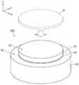
도 1 은 제 1 실시형태에 있어서의 정전 척 (100) 의 외관 구성을 개략적으로 나타내는 사시도이다.
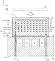
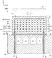
도 2 는 제 1 실시형태에 있어서의 정전 척 (100) 의 XZ 단면 구성을 개략적으로 나타내는 설명도이다.
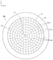
도 3 은 제 1 실시형태에 있어서의 정전 척 (100) 의 XY 평면 구성을 개략적으로 나타내는 설명도이다.
도 4 는 제 1 실시형태에 있어서의 정전 척 (100) 의 발열용 저항체층 (50), 발열 저항체용 드라이버 (51), 측온용 저항체층 (60), 및 측온 저항체용 드라이버 (70) 의 구성을 모식적으로 나타내는 설명도이다.
도 5 는 1 개의 세그먼트 (SE) 에 배치된 1 개의 발열용 저항체 (500) 의 XY 단면 구성을 모식적으로 나타내는 설명도이다.
도 6 은 1 개의 세그먼트 (SE) 에 배치된 1 개의 측온용 저항체 (600) 를 구성하는 제 1 저항체 요소 (610) 의 XY 단면 구성을 모식적으로 나타내는 설명도이다.
도 7 은 제 1 실시형태의 변형예에 있어서의 정전 척 (100) 의 발열용 저항체층 (50), 발열 저항체용 드라이버 (51), 측온용 저항체층 (60), 및 측온 저항체용 드라이버 (70) 의 구성을 모식적으로 나타내는 설명도이다.
도 8 은 제 2 실시형태에 있어서의 정전 척 (100a) 의 발열용 저항체층 (50), 발열 저항체용 드라이버 (51), 측온용 저항체층 (60), 및 측온 저항체용 드라이버 (70) 의 구성을 모식적으로 나타내는 설명도이다.
도 9 는 제 3 실시형태에 있어서의 정전 척 (100b) 의 XZ 단면 구성을 개략적으로 나타내는 설명도이다.
도 10 은 제 3 실시형태에 있어서의 정전 척 (100b) 의 발열용 저항체층 (50), 발열 저항체용 드라이버 (51), 측온용 저항체층 (60), 및 측온 저항체용 드라이버 (70) 의 구성을 모식적으로 나타내는 설명도이다.
도 11 은 제 4 실시형태에 있어서의 정전 척 (100c) 의 XZ 단면 구성을 개략적으로 나타내는 설명도이다.
도 12 는 제 4 실시형태에 있어서의 정전 척 (100c) 의 측온 저항체용 드라이버 (70) 의 XY 평면 구성을 모식적으로 나타내는 설명도이다.1 is a perspective view schematically showing an external configuration of an
2 is an explanatory diagram schematically showing an XZ cross-sectional configuration of the
3 is an explanatory diagram schematically showing the XY plane configuration of the
FIG. 4 shows the configuration of the heat generating
FIG. 5: is explanatory drawing which shows typically the XY cross-sectional structure of one
FIG. 6: is explanatory drawing which shows typically the XY cross-sectional structure of the
Fig. 7 shows a heat generating
FIG. 8 shows the configuration of the heat generating
FIG. 9 is an explanatory diagram schematically showing an XZ cross-sectional configuration of the
FIG. 10 shows the configuration of the heat generating
FIG. 11 is an explanatory diagram schematically showing an XZ cross-sectional configuration of the electrostatic chuck 100c in the fourth embodiment.
FIG. 12: is explanatory drawing which shows typically the XY plane structure of the
A. 제 1 실시형태 : A. First Embodiment
A-1. 정전 척 (100) 의 구성 : A-1. Configuration of the electrostatic chuck 100:
도 1 은, 제 1 실시형태에 있어서의 정전 척 (100) 의 외관 구성을 개략적으로 나타내는 사시도이고, 도 2 는, 제 1 실시형태에 있어서의 정전 척 (100) 의 XZ 단면 구성을 개략적으로 나타내는 설명도이고, 도 3 은, 제 1 실시형태에 있어서의 정전 척 (100) 의 XY 평면 (상면) 구성을 개략적으로 나타내는 설명도이다. 각 도면에는, 방향을 특정하기 위한 서로 직교하는 XYZ 축이 도시되어 있다. 본 명세서에서는, 편의적으로, Z 축 정 (正) 방향을 상방향이라고 하고, Z 축 부 (負) 방향을 하방향이라고 하기로 하지만, 정전 척 (100) 은 실제로는 그러한 방향과는 상이한 방향으로 설치되어도 된다.1 is a perspective view schematically showing an external configuration of an
정전 척 (100) 은, 대상물 (예를 들어 웨이퍼 (W)) 을 정전 인력에 의해 흡착하여 유지하는 장치로, 예를 들어 반도체 제조 장치의 진공 챔버 내에서 웨이퍼 (W) 를 고정시키기 위해서 사용된다. 정전 척 (100) 은, 소정의 배열 방향 (본 실시형태에서는 상하 방향 (Z 축 방향)) 으로 나란하게 배치된 세라믹스판 (10) 및 베이스 부재 (20) 를 구비한다. 세라믹스판 (10) 과 베이스 부재 (20) 는, 세라믹스판 (10) 의 하면 (S2) (도 2 참조) 과 베이스 부재 (20) 의 상면 (S3) 이 상기 배열 방향으로 대향하도록 배치된다.The
세라믹스판 (10) 은, 상기 서술한 배열 방향 (Z 축 방향) 과 대략 직교하는 대략 원형 평면상의 상면 (이하, 「흡착면」이라고 한다) (S1) 을 갖는 판상 부재로, 세라믹스 (예를 들어, 알루미나나 질화알루미늄 등) 에 의해 형성되어 있다. 세라믹스판 (10) 의 직경은 예를 들어 50 ㎜ ∼ 500 ㎜ 정도 (통상은 200 ㎜ ∼ 350 ㎜ 정도) 이고, 세라믹스판 (10) 의 두께는 예를 들어 1 ㎜ ∼ 10 ㎜ 정도이다. 세라믹스판 (10) 의 흡착면 (S1) 은, 특허청구범위에 있어서의 제 1 표면에 상당하고, Z 축 방향은, 특허청구범위에 있어서의 제 1 방향에 상당한다. 또, 본 명세서에서는, Z 축 방향과 직교하는 방향을 「면방향」이라고 한다.The
도 2 에 나타내는 바와 같이, 세라믹스판 (10) 의 내부에는, 도전성 재료 (예를 들어, 텅스텐, 몰리브덴, 백금 등) 에 의해 형성된 척 전극 (40) 이 배치되어 있다. Z 축 방향에서 볼 때의 척 전극 (40) 의 형상은, 예를 들어 대략 원형이다. 척 전극 (40) 에 전원 (도시 생략) 으로부터 전압이 인가되면, 정전 인력이 발생하고, 이 정전 인력에 의해 웨이퍼 (W) 가 세라믹스판 (10) 의 흡착면 (S1) 에 흡착 고정된다.As shown in FIG. 2, the
세라믹스판 (10) 의 내부에는, 또한, 각각 도전성 재료 (예를 들어, 텅스텐, 몰리브덴, 백금 등) 에 의해 형성된, 발열용 저항체층 (50) 과, 발열 저항체용 드라이버 (51) 와, 측온용 저항체층 (60) 과, 측온 저항체용 드라이버 (70) 와, 각종 비아가 배치되어 있다. 본 실시형태에서는, 발열용 저항체층 (50) 은 척 전극 (40) 보다 하측에 배치되고, 발열 저항체용 드라이버 (51) 는 발열용 저항체층 (50) 보다 하측에 배치되고, 측온용 저항체층 (60) 은, 발열 저항체용 드라이버 (51) 보다 하측에 배치되고, 측온 저항체용 드라이버 (70) 는 측온용 저항체층 (60) 보다 하측에 배치되어 있다. 이들의 구성에 대해서는, 나중에 상세히 서술한다. 또한, 이와 같은 구성의 세라믹스판 (10) 은, 예를 들어, 세라믹스 그린 시트를 복수 장 제조하고, 소정의 세라믹스 그린 시트에 비아 구멍의 형성이나 메탈라이즈 페이스트의 인쇄 등의 가공을 실시하여, 이들 세라믹스 그린 시트를 열 압착하고, 절단 등의 가공을 실시한 다음 소성함으로써 제조할 수 있다.Inside the
베이스 부재 (20) 는, 예를 들어 세라믹스판 (10) 과 같은 직경의, 또는 세라믹스판 (10) 보다 직경이 큰 원형 평면의 판상 부재이고, 예를 들어 금속 (알루미늄이나 알루미늄 합금 등) 에 의해 형성되어 있다. 베이스 부재 (20) 의 직경은 예를 들어 220 ㎜ ∼ 550 ㎜ 정도 (통상은 220 ㎜ ∼ 350 ㎜) 이고, 베이스 부재 (20) 의 두께는 예를 들어 20 ㎜ ∼ 40 ㎜ 정도이다.The
베이스 부재 (20) 는, 세라믹스판 (10) 의 하면 (S2) 과 베이스 부재 (20) 의 상면 (S3) 사이에 배치된 접착층 (30) 에 의해, 세라믹스판 (10) 에 접합되어 있다. 접착층 (30) 은, 예를 들어 실리콘계 수지나 아크릴계 수지, 에폭시계 수지 등의 접착재에 의해 구성되어 있다. 접착층 (30) 의 두께는, 예를 들어 0.1 ㎜ ∼ 1 ㎜ 정도이다.The
베이스 부재 (20) 의 내부에는 냉매 유로 (21) 가 형성되어 있다. 냉매 유로 (21) 에 냉매 (예를 들어, 불소계 불활성 액체나 물 등) 가 흐르면, 베이스 부재 (20) 가 냉각되고, 접착층 (30) 을 개재한 베이스 부재 (20) 와 세라믹스판 (10) 사이의 전열 (열 흡수) 에 의해 세라믹스판 (10) 이 냉각되어, 세라믹스판 (10) 의 흡착면 (S1) 에 유지된 웨이퍼 (W) 가 냉각된다. 이로써, 웨이퍼 (W) 의 온도 제어가 실현된다.The
A-2. 발열용 저항체층 (50) 및 발열 저항체용 드라이버 (51) 의 구성 : A-2. Configuration of the heat generating
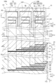
상기 서술한 바와 같이, 세라믹스판 (10) 의 내부에는, 발열용 저항체층 (50) 와 발열 저항체용 드라이버 (51) 가 배치되어 있다 (도 2 참조). 도 4 는, 발열용 저항체층 (50) 및 발열 저항체용 드라이버 (51) 의 구성 (및 측온용 저항체층 (60), 측온 저항체용 드라이버 (70) 의 구성) 을 모식적으로 나타내는 설명도이다. 도 4 의 상단에는, 발열용 저항체층 (50) 의 일부의 XZ 단면 구성이 모식적으로 나타나 있고, 도 4 의 중단에는, 발열 저항체용 드라이버 (51) 의 일부의 XY 평면 구성이 모식적으로 나타나 있다.As described above, the heat generating
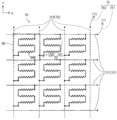
여기서, 도 3 에 나타내는 바와 같이, 본 실시형태의 정전 척 (100) 에서는, 세라믹스판 (10) 이, 면 방향 (Z 축 방향과 직교하는 방향) 으로 나란한 복수의 세그먼트 (SE) 로 가상적으로 분할되어 있다. 보다 구체적으로는, Z 축 방향에서 볼 때, 세라믹스판 (10) 이, 흡착면 (S1) 의 중심점 (P1) 을 중심으로 하는 동심원상의 복수의 제 1 경계선 (BL1) 에 의해 복수의 가상적인 환상 영역 (단, 중심점 (P1) 을 포함하는 영역만은 원형상 영역) 으로 분할되고, 또한 각 환상 영역이, 흡착면 (S1) 의 직경 방향으로 연장되는 복수의 제 2 경계선 (BL2) 에 의해 흡착면 (S1) 의 원주 방향으로 나란한 복수의 가상적인 영역인 세그먼트 (SE) 로 분할되어 있다.As shown in FIG. 3, in the
도 4 에 나타내는 바와 같이, 발열용 저항체층 (50) 은, 복수의 발열용 저항체 (500) 를 포함하고 있다. 복수의 발열용 저항체 (500) 의 각각은, 세라믹스판 (10) 에 설정된 복수의 세그먼트 (SE) 의 하나에 배치되어 있다. 즉, 본 실시형태의 정전 척 (100) 에서는, 복수의 세그먼트 (SE) 의 각각에, 1 개의 발열용 저항체 (500) 가 배치되어 있다.As shown in FIG. 4, the heat generating
도 5 는, 1 개의 세그먼트 (SE) 에 배치된 1 개의 발열용 저항체 (500) 의 XY 단면 구성을 모식적으로 나타내는 설명도이다. 도 5 에 나타내는 바와 같이, 발열용 저항체 (500) 는, 발열용 저항체 (500) 의 양단을 구성하는 1 쌍의 패드부 (504) 와, 1 쌍의 패드부 (504) 의 사이를 연결하는 선상의 저항선부 (502) 를 구비한다. 본 실시형태에서는, 저항선부 (502) 는, Z 축 방향에서 볼 때, 세그먼트 (SE) 내의 각 위치를 가능한 한 치우침없이 통과하는 형상으로 되어 있다. 다른 세그먼트 (SE) 에 배치된 발열용 저항체 (500) 의 구성도 동일하다.FIG. 5: is explanatory drawing which shows typically the XY cross-sectional structure of one
또, 정전 척 (100) 은, 각 발열용 저항체 (500) 에 대한 급전을 위한 구성을 구비하고 있다. 구체적으로는, 정전 척 (100) 에는, 1 쌍의 단자용 구멍 (도시 생략) 이 형성되어 있고, 각 단자용 구멍에는 급전 단자 (도시 생략) 가 수용되어 있다.Moreover, the
또, 상기 서술한 발열 저항체용 드라이버 (51) 도, 각 발열용 저항체 (500) 에 대한 급전을 위한 구성의 일부이다. 도 4 에 나타내는 바와 같이, 발열 저항체용 드라이버 (51) 는, 제 1 도전 라인 (511) 및 제 2 도전 라인 (512) 으로 구성된 복수의 라인쌍 (510) 을 포함하고 있다. 또한, 도 4 에 나타내는 예에서는, 제 2 도전 라인 (512) 은, 복수의 라인쌍 (510) 에 공유되어 있다. 라인쌍 (510) 마다 개별적인 제 2 도전 라인 (512) 이 준비되어도 된다. 제 1 도전 라인 (511) 및 제 2 도전 라인 (512) 의 각각은, 비아나 전극 패드 (모두 도시 생략) 등을 통해 서로 상이한 급전 단자에 전기적으로 접속되어 있다.In addition, the above-described heat generating
또, 도 4 및 도 5 에 나타내는 바와 같이, 1 개의 라인쌍 (510) 을 구성하는 제 1 도전 라인 (511) 은, 비아쌍 (53) 을 구성하는 일방의 비아 (531) 를 통해, 발열용 저항체 (500) 의 일단 (패드부 (504)) 에 전기적으로 접속되어 있고, 그 라인쌍 (510) 을 구성하는 제 2 도전 라인 (512) 은, 그 비아쌍 (53) 을 구성하는 타방의 비아 (532) 를 통해, 그 발열용 저항체 (500) 의 타단 (패드부 (504)) 에 전기적으로 접속되어 있다.4 and 5, the first
전원 (도시 생략) 으로부터 급전 단자, 전극 패드, 비아, 라인쌍 (510), 및 비아쌍 (53) 을 통해 발열용 저항체 (500) 에 전압이 인가되면, 발열용 저항체 (500) 가 발열한다. 이로써, 발열용 저항체 (500) 가 배치된 세그먼트 (SE) 가 가열된다. 세라믹스판 (10) 의 각 세그먼트 (SE) 에 배치된 발열용 저항체 (500) 에 대한 인가 전압을 개별적으로 제어함으로써, 각 세그먼트 (SE) 의 온도를 개별적으로 제어할 수 있다.When a voltage is applied to the
A-3. 측온용 저항체층 (60) 및 측온 저항체용 드라이버 (70) 의 구성 : A-3. Configuration of the
상기 서술한 바와 같이, 세라믹스판 (10) 의 내부에는, 측온용 저항체층 (60) 과 측온 저항체용 드라이버 (70) 가 배치되어 있다 (도 2 참조). 도 4 의 상단에는, 측온용 저항체층 (60) 의 일부의 XZ 단면 구성이 모식적으로 나타나 있고, 도 4 의 하단에는, 측온 저항체용 드라이버 (70) 의 일부의 XY 평면 구성이 모식적으로 나타나 있다. 또한, 측온 저항체용 드라이버 (70) 는, 특허청구범위에 있어서의 드라이버에 상당한다.As described above, the
도 2 및 도 4 에 나타내는 바와 같이, 측온용 저항체층 (60) 은, Z 축 방향에 있어서의 위치가 서로 상이한 3 개의 층 (상측에서부터 순서대로 제 1 저항체층 (61), 제 2 저항체층 (62), 제 3 저항체층 (63)) 으로 구성되어 있다. 도 4 에 나타내는 바와 같이, 이와 같은 3 개의 층으로 구성된 측온용 저항체층 (60) 은, 복수의 측온용 저항체 (600) 를 포함하고 있다. 복수의 측온용 저항체 (600) 의 각각은, 세라믹스판 (10) 에 설정된 복수의 세그먼트 (SE) 의 하나에 배치되어 있다. 즉, 본 실시형태의 정전 척 (100) 에서는, 복수의 세그먼트 (SE) 의 각각에, 1 개의 측온용 저항체 (600) 가 배치되어 있다. 또한, 상기 서술한 바와 같이, 본 실시형태의 정전 척 (100) 에서는, 측온용 저항체층 (60) 은 발열용 저항체층 (50) 보다 하측에 위치하기 때문에, 각 세그먼트 (SE) 에 있어서, 측온용 저항체 (600) 는, 발열용 저항체 (500) 보다 하측 (즉, 발열용 저항체 (500) 와 비교하여 베이스 부재 (20) 에 가까운 쪽) 에 위치한다.As shown in FIG. 2 and FIG. 4, the resistance-
도 4 에 나타내는 바와 같이, 각 측온용 저항체 (600) 는, 제 1 저항체층 (61) 에 포함되는 제 1 저항체 요소 (610) 와, 제 2 저항체층 (62) 에 포함되는 제 2 저항체 요소 (620) 와, 제 3 저항체층 (63) 에 포함되는 제 3 저항체 요소 (630) 를 포함하고 있다. 도 6 은, 1 개의 세그먼트 (SE) 에 배치된 1 개의 측온용 저항체 (600) 를 구성하는 제 1 저항체 요소 (610) 의 XY 단면 구성을 모식적으로 나타내는 설명도이다. 도 6 에는, 참고를 위해, 동일 세그먼트 (SE) 에 배치된 발열용 저항체 (500) 의 면방향의 위치를 파선으로 나타내고 있다. 도 6 에 나타내는 바와 같이, 제 1 저항체 요소 (610) 는, 제 1 저항체 요소 (610) 의 양단을 구성하는 1 쌍의 패드부 (614) 와, 1 쌍의 패드부 (614) 의 사이를 연결하는 선상의 저항선부 (612) 를 구비한다. 또한, 측온용 저항체 (600) 를 구성하는 다른 저항체 요소 (제 2 저항체 요소 (620) 및 제 3 저항체 요소 (630)) 의 구성은, 도 6 에 나타내는 제 1 저항체 요소 (610) 의 구성과 동일하다. 즉, 제 2 저항체 요소 (620) 및 제 3 저항체 요소 (630) 의 각각은, 1 쌍의 패드부와, 1 쌍의 패드부의 사이를 연결하는 선상의 저항선부를 구비하고 있다. 또한, 제 2 저항체 요소 (620) 및 제 3 저항체 요소 (630) 의 패드부나 저항선부의 위치나 형상은, 반드시 제 1 저항체 요소 (610) 의 패드부나 저항선부의 위치나 형상과 동일하지 않아도 된다.As shown in FIG. 4, each
도 4 에 나타내는 바와 같이, 제 1 저항체 요소 (610) 의 일방의 단부 (P12) (구체적으로는, 상기 서술한 패드부 (614)) 는, 비아 (64) 를 통해, 제 2 저항체 요소 (620) 의 일방의 단부 (P22) 에 전기적으로 접속되어 있다. 또, 제 2 저항체 요소 (620) 의 타방의 단부 (P21) 는, 다른 비아 (65) 를 통해, 제 3 저항체 요소 (630) 의 일방의 단부 (P31) 에 전기적으로 접속되어 있다. 즉, 측온용 저항체 (600) 를 구성하는 3 개의 저항체 요소 (제 1 저항체 요소 (610), 제 2 저항체 요소 (620), 제 3 저항체 요소 (630)) 는, 서로 직렬로 접속되어 있다.As shown in FIG. 4, one end P12 (specifically, the
또, 정전 척 (100) 은, 각 측온용 저항체 (600) 에 대한 급전을 위한 구성을 구비하고 있다. 구체적으로는, 도 2 에 나타내는 바와 같이, 정전 척 (100) 에는, 베이스 부재 (20) 의 하면 (S4) 으로부터 세라믹스판 (10) 의 내부에 이르는 1 쌍의 단자용 구멍 (22) 이 형성되어 있고, 각 단자용 구멍 (22) 에는 급전 단자 (12) 가 수용되어 있다.Moreover, the
또, 상기 서술한 측온 저항체용 드라이버 (70) 도, 각 측온용 저항체 (600) 에 대한 급전을 위한 구성의 일부이다. 도 4 에 나타내는 바와 같이, 측온 저항체용 드라이버 (70) 는, 제 1 도전 라인 (711) 및 제 2 도전 라인 (712) 으로 구성된 복수의 라인쌍 (710) 을 포함하고 있다. 도 2 및 도 4 에 나타내는 바와 같이, 라인쌍 (710) 을 구성하는 제 1 도전 라인 (711) 은, 급전측 비아쌍 (75) 을 구성하는 일방의 급전측 비아 (751), 및 전극 패드쌍 (77) 을 구성하는 일방의 전극 패드 (771) 를 통해, 일방의 급전 단자 (12) 에 전기적으로 접속되어 있고, 그 라인쌍 (710) 을 구성하는 제 2 도전 라인 (712) 은, 그 급전측 비아쌍 (75) 을 구성하는 타방의 급전측 비아 (752), 및 그 전극 패드쌍 (77) 을 구성하는 타방의 전극 패드 (772) 를 통해, 타방의 급전 단자 (12) 에 전기적으로 접속되어 있다. 또한, 도 4 에는, 1 개의 라인쌍 (710) 에 대한 급전측 비아쌍 (75) 을 대표적으로 도시하고, 다른 라인쌍 (710) 에 대한 급전측 비아쌍 (75) 의 도시를 생략하였다. 급전측 비아 (751) 는, 특허청구범위에 있어서의 제 1 급전측 비아에 상당하고, 급전측 비아 (752) 는, 특허청구범위에 있어서의 제 2 급전측 비아에 상당한다.Moreover, the above-mentioned
또, 도 2, 도 4 및 도 6 에 나타내는 바와 같이, 라인쌍 (710) 을 구성하는 제 1 도전 라인 (711) 은, 저항체측 비아쌍 (73) 을 구성하는 일방의 저항체측 비아 (731) 를 통해, 측온용 저항체 (600) 의 일단 (보다 상세하게는, 측온용 저항체 (600) 를 구성하는 제 1 저항체 요소 (610) 의 하나의 단부 (P11) 인 패드부 (614)) 에 전기적으로 접속되어 있고, 그 라인쌍 (710) 을 구성하는 제 2 도전 라인 (712) 은, 그 저항체측 비아쌍 (73) 을 구성하는 타방의 저항체측 비아 (732) 를 통해, 그 측온용 저항체 (600) 의 타단 (보다 상세하게는, 측온용 저항체 (600) 를 구성하는 제 3 저항체 요소 (630) 의 하나의 단부 (P32) 인 패드부) 에 전기적으로 접속되어 있다. 저항체측 비아 (731) 는, 특허청구범위에 있어서의 제 1 저항체측 비아에 상당하고, 저항체측 비아 (732) 는, 특허청구범위에 있어서의 제 2 저항체측 비아에 상당한다.2, 4, and 6, the first
전원 (도시 생략) 으로부터 1 쌍의 급전 단자 (12), 전극 패드쌍 (77), 급전측 비아쌍 (75), 라인쌍 (710), 및 저항체측 비아쌍 (73) 을 통해 측온용 저항체 (600) 에 전압이 인가되면, 측온용 저항체 (600) 에 전류가 흐른다. 측온용 저항체 (600) 는, 온도가 변화하면 저항값이 변화하는 도전성 재료 (예를 들어, 텅스텐, 몰리브덴, 백금 등) 에 의해 형성되어 있다. 구체적으로는, 측온용 저항체 (600) 는, 온도가 높아질수록 저항값이 높아진다. 또, 정전 척 (100) 은, 측온용 저항체 (600) 에 인가된 전압과 측온용 저항체 (600) 에 흐르는 전류를 측정하기 위한 구성 (예를 들어, 전압계나 전류계 (모두 도시 생략)) 를 가지고 있다. 그 때문에, 본 실시형태의 정전 척 (100) 에서는, 측온용 저항체 (600) 의 전압의 측정치와 측온용 저항체 (600) 의 전류의 측정치에 기초하여, 측온용 저항체 (600) 의 온도를 측정 (특정) 할 수 있다.A resistor for temperature measurement from a power supply terminal (not shown) through a pair of
상기 서술한 방법에 의해 세라믹스판 (10) 에 배치된 각 측온용 저항체 (600) 의 온도를 개별적으로 측정함으로써, 세라믹스판 (10) 의 각 세그먼트 (SE) 의 온도를 실시간으로 개별적으로 측정할 수 있다. 그 때문에, 본 실시형태의 정전 척 (100) 에서는, 세라믹스판 (10) 의 각 세그먼트 (SE) 의 온도 측정 결과에 기초하여, 각 세그먼트 (SE) 에 배치된 발열용 저항체 (500) 에 대한 인가 전압을 개별적으로 제어함으로써, 각 세그먼트 (SE) 의 온도를 높은 정밀도로 제어할 수 있다. 따라서, 본 실시형태의 정전 척 (100) 에 의하면, 세라믹스판 (10) 의 흡착면 (S1) 의 온도 분포의 균일성 (즉, 웨이퍼 (W) 의 온도 분포의 균일성) 을 향상시킬 수 있다. 또한, 상기 서술한 발열용 저항체 (500) 및 측온용 저항체 (600) 에 대한 급전 경로를 형성하기 위한 구성을, 일괄하여 급전부 (80) 라고 부른다 (도 2 참조).By individually measuring the temperature of the resistance thermometer for temperature measurement arranged on the
여기서, 도 6 에는, Z 축 방향과 평행한 가상 평면 (VS) (보다 구체적으로는, X 축에 평행한 가상 평면 (VS)) 에, 측온용 저항체 (600) 를 구성하는 제 1 저항체 요소 (610) 와, 그 측온용 저항체 (600) 와 동일 세그먼트 (SE) 에 배치된 발열용 저항체 (500) 를 투영했을 때의, 제 1 저항체 요소 (610) 의 투영 (投影) (601) 과, 발열용 저항체 (500) 의 투영 (501) 이 나타나 있다. 도 6 에 나타내는 바와 같이, 제 1 저항체 요소 (610) 의 투영 (601) 의 양단 (EP11, EP12) 의 위치는, 발열용 저항체 (500) 의 투영 (501) 의 양단 (EP21, EP22) 사이의 위치로 되어 있다. 이와 같이, 본 실시형태의 정전 척 (100) 에서는, Z 축 방향과 평행한 임의의 가상 평면 (VS) 에, 제 1 저항체 요소 (610) 와, 그 측온용 저항체 (600) 와 동일 세그먼트 (SE) 에 배치된 발열용 저항체 (500) 를 투영했을 때, 가상 평면 (VS) 에 평행하며, 또한 Z 축 방향과 직교하는 방향 (도 6 의 예에서는 X 축 방향) 에 있어서, 제 1 저항체 요소 (610) 의 투영의 양단의 위치는, 발열용 저항체 (500) 의 투영의 양단 사이의 위치이다.6 shows a first resistor element constituting the
또, 제 2 저항체 요소 (620) 및 제 3 저항체 요소 (630) 에 대해서도, 동일하게, 제 2 저항체 요소 (620) (또는 제 3 저항체 요소 (630)) 의 투영의 양단의 위치는, 발열용 저항체 (500) 의 투영의 양단 사이의 위치이다. 따라서, 3 개의 저항체 요소 (제 1 저항체 요소 (610), 제 2 저항체 요소 (620), 제 3 저항체 요소 (630)) 로 구성된 측온용 저항체 (600) 에 대해서도, Z 축 방향과 평행한 임의의 가상 평면에, 측온용 저항체 (600) 와, 그 측온용 저항체 (600) 와 동일 세그먼트 (SE) 내에 배치된 발열용 저항체 (500) 를 투영했을 때, 가상 평면에 평행하며, 또한 Z 축 방향과 직교하는 방향에 있어서, 측온용 저항체 (600) 의 투영의 양단의 위치는, 발열용 저항체 (500) 의 투영의 양단 사이의 위치가 된다. 또한, 이와 같은 특징은, 측온용 저항체 (600) 가, Z 축 방향에서 볼 때, 그 측온용 저항체 (600) 와 동일 세그먼트 (SE) 에 배치된 발열용 저항체 (500) 와 비교하여, 세그먼트 (SE) 에 있어서의, 보다 내측의 위치 (세그먼트 (SE) 의 경계로부터 보다 먼 위치) 에 배치되어 있는 것을 의미한다.Similarly with respect to the
또, 도 4 에 나타내는 바와 같이, 본 실시형태의 정전 척 (100) 에서는, 측온 저항체용 드라이버 (70) 에 포함되는 각 도전 라인 (제 1 도전 라인 (711) 또는 제 2 도전 라인 (712)) 의 선폭이 서로 동일하지 않다. 보다 상세하게는, 도전 라인 (711, 712) 의 길이 (L) 가 길수록, 도전 라인 (711, 712) 의 선폭 (W) 이 굵어지고 있다. 예를 들어, 도 4 에 나타내는 측온 저항체용 드라이버 (70) 에 포함되는 6 개의 도전 라인 (711, 712) 의 길이를 도면의 상측에 나타낸 것부터 순서대로 L1, L2, L3, L4, L5, L6 으로 하고, 그들의 선폭을 동일 순서대로 W1, W2, W3, W4, W5, W6 으로 하면, 이하의 관계 (1) 및 (2) 가 성립되어 있다. 그 때문에, 측온 저항체용 드라이버 (70) 에 포함되는 각 도전 라인 (711, 712) 의 저항값은, 서로 가까운 값으로 되어 있다. 또한, 도전 라인 (711, 712) 의 길이 (L) 란, 그 도전 라인 (711, 712) 에 있어서의 하나의 도전 부재 (예를 들어, 측온용 저항체 (600)) 와의 접속을 위한 비아의 중심 (비아가 복수 존재하는 경우에는, 복수의 비아의 중심점을 정점으로 하는 다각형의 도심 (圖心)) 으로부터, 그 도전 라인 (711, 712) 에 있어서의 다른 도전 부재 (예를 들어, 전극 패드 (771)) 와의 접속을 위한 비아의 중심 (동일) 까지의, 연신 방향을 따른 치수 (크기) 를 의미한다. 또, 도전 라인 (711, 712) 의 폭 (W) 이란, 그 도전 라인 (711, 712) 의 연신 방향과 직교하는 방향을 따른 치수 (크기) 를 의미한다.In addition, as shown in FIG. 4, in the
L1 < L2 < L3 < L4 < L5 < L6 ··· (1) L1 <L2 <L3 <L4 <L5 <L6 ... (1)
W1 < W2 < W3 < W4 < W5 < W6 ··· (2) W1 <W2 <W3 <W4 <W5 <W6 ... (2)
또, 도 4 에 나타내는 바와 같이, 본 실시형태의 정전 척 (100) 에서는, 측온 저항체용 드라이버 (70) 에 포함되는 라인쌍 (710) 을 구성하는 제 1 도전 라인 (711) 및 제 2 도전 라인 (712) 의 선폭은, 그 라인쌍 (710) 에 전기적으로 접속된 측온용 저항체 (600) 의 선폭 (구체적으로는, 측온용 저항체 (600) 를 구성하는 제 1 저항체 요소 (610), 제 2 저항체 요소 (620), 제 3 저항체 요소 (630) 의 저항선부의 선폭) 보다 굵어지고 있다. 예를 들어, 도 4 에 나타난 3 개의 세그먼트 (SE) 중, 가장 좌측에 위치하는 세그먼트 (SE) 에 배치된 측온용 저항체 (600) 에 전기적으로 접속된 라인쌍 (710) 을 구성하는 제 1 도전 라인 (711) 의 선폭 (W5) 및 제 2 도전 라인 (712) 의 선폭 (W6) 은, 모두, 그 측온용 저항체 (600) 의 선폭보다 굵어지고 있다.In addition, as shown in FIG. 4, in the
또한, 발열용 저항체 (500) 와, 측온용 저항체 (600) 와, 발열 저항체용 드라이버 (51) 와, 측온 저항체용 드라이버 (70) 는, 하기의 관점 중 적어도 하나에 있어서 서로 상이하다. In addition, the
(1) 재료의 비저항 (Ω·m) 에 대해 (1) About the specific resistance (Ωm) of the material
발열 저항체용 드라이버 (51) 의 재료의 비저항은, 발열용 저항체 (500) 의 재료의 비저항의 95 % 이하이다.The specific resistance of the material of the heat generating
측온 저항체용 드라이버 (70) 의 재료의 비저항은, 측온용 저항체 (600) 의 재료의 비저항의 95 % 이하이다.The specific resistance of the material of the
(2) 재료의 저항 온도 계수 (ppm/℃) 에 대해(2) About resistance temperature coefficient (ppm / ° C) of the material
측온용 저항체 (600) 의 재료의 저항 온도 계수는, 발열용 저항체 (500) 의 재료의 저항 온도 계수의 110 % 이상이다. The resistance temperature coefficient of the material of the resistance thermometer for temperature measurement is 110% or more of the resistance temperature coefficient of the material of the
측온용 저항체 (600) 의 재료의 저항 온도 계수는, 측온 저항체용 드라이버 (70) 의 재료의 저항 온도 계수의 110 % 이상이다.The resistance temperature coefficient of the material of the
(3) 패턴 형상에 대해 (3) About pattern shape
발열용 저항체 (500) 는, 세그먼트 (SE) 전체에 균일적인 피치로 배선되고, 온도 평활화를 위해, 온도 특이점이 없도록, 일부분이 패턴 폭 조정되어 있다. 또, 발열용 저항체 (500) 는, 저항을 높게 하기 위해서, 상하 방향으로 나란한 복수층의 요소가 직렬 접속된 구성이어도 된다.The
측온용 저항체 (600) 는, 세그먼트 (SE) 의 온도를 측정하고자 하는 포인트를 중심으로 배선된다. 세그먼트 (SE) 간의 경계에는, 인접 세그먼트 (SE) 의 온도 영향이 있기 때문에, 측온용 저항체 (600) 는, 그 경계를 가능한 한 피해서 배선된다. 측온용 저항체 (600) 는, 온도 특이점에 대한 패턴 조정이 필요 없기 때문에, 측온용 저항체 (600) 의 선폭은, 발열용 저항체 (500) 의 선폭과 비교하여, 가늘며, 또한 균일화되어 있다. 측온용 저항체 (600) 는, 저항을 높게 하기 위해서, 상하 방향으로 나란한 복수층의 요소가 직렬 접속된 구성이어도 된다. The
발열 저항체용 드라이버 (51) 는, 발열용 저항체 (500) 와의 접속 지점 (비아) 으로부터 급전 단자와의 접속 지점 (비아) 까지, 가능한 한 최단 루트로, 또한 굵은 폭으로 배선되고, 되접히는 지점 등은 존재하지 않는다. 발열 저항체용 드라이버 (51) 는, 저항을 낮게 하기 위해서, 상하 방향으로 나란한 복수층의 요소가 병렬 접속된 구성이어도 된다. 또한, 발열 저항체용 드라이버 (51) 는, 발열용 저항체 (500) 와의 접속 지점 (비아) 으로부터 급전 단자와의 접속 지점 (비아) 까지의 사이에 장애물이 있는 경우에는, 상하 방향으로 나란한 복수층의 요소가 직렬 접속된 구성이어도 된다.The heat
측온 저항체용 드라이버 (70) 는, 발열 저항체용 드라이버 (51) 와 마찬가지로, 측온용 저항체 (600) 와의 접속 지점 (비아) 으로부터 급전 단자와의 접속 지점 (비아) 까지, 가능한 한 최단 루트로, 또한 굵은 폭으로 배선되고, 되접히는 지점 등은 존재하지 않는다. 측온 저항체용 드라이버 (70) 는, 저항을 낮게 하기 위해서, 상하 방향으로 나란한 복수층의 요소가 병렬 접속된 구성이어도 된다. 또한, 측온 저항체용 드라이버 (70) 는, 측온용 저항체 (600) 와의 접속 지점 (비아) 으로부터 급전 단자와의 접속 지점 (비아) 까지의 사이에 장애물이 있는 경우에는, 상하 방향으로 나란한 복수층의 요소가 직렬 접속된 구성이어도 된다.The driver for
A-4. 본 실시형태의 효과 : A-4. Effect of this embodiment:
이상 설명한 바와 같이, 제 1 실시형태의 정전 척 (100) 은, Z 축 방향과 대략 직교하는 대략 평면상의 흡착면 (S1) 을 갖는 세라믹스판 (10) 을 구비하고, 세라믹스판 (10) 의 흡착면 (S1) 상에 대상물 (예를 들어 웨이퍼 (W)) 을 유지하는 유지 장치이다. 정전 척 (100) 은, 세라믹스판 (10) 을 면방향으로 나란한 복수의 세그먼트 (SE) 로 가상적으로 분할했을 때의 각 세그먼트 (SE) 내에 배치된 발열용 저항체 (500) 및 측온용 저항체 (600) 와, 발열용 저항체 (500) 및 측온용 저항체 (600) 에 대한 급전 경로를 구성하는 급전부 (80) 를 구비한다. 각 세그먼트 (SE) 에 있어서, 측온용 저항체 (600) 의 Z 축 방향에 있어서의 위치는, 발열용 저항체 (500) 의 위치와는 상이하다. 또, 제 1 실시형태의 정전 척 (100) 에서는, 각 측온용 저항체 (600) 는, Z 축 방향에 있어서의 위치가 서로 상이하며, 또한 서로 직렬로 접속된 3 층의 저항체 요소 (제 1 저항체 요소 (610), 제 2 저항체 요소 (620), 제 3 저항체 요소 (630)) 를 갖는다. 그 때문에, 제 1 실시형태의 정전 척 (100) 에서는, 측온용 저항체 (600) 가 단층 구성인 형태와 비교하여, 측온용 저항체 (600) 를 1 개의 세그먼트 (SE) 내에 수용하면서, 그 저항값을 높게 할 수 있다. 측온용 저항체 (600) 의 저항값이 높아지면, 측온용 저항체 (600) 의 저항값에 기초하는 온도 측정의 분해능 (감도) 은 향상된다. 따라서, 제 1 실시형태의 정전 척 (100) 에 의하면, 측온용 저항체 (600) 의 저항값에 기초하는 온도 측정의 분해능을 향상시키는 것에 의해 세라믹스판 (10) 의 각 세그먼트 (SE) 의 온도 측정의 정밀도를 향상시킬 수 있어, 각 세그먼트 (SE) 에 배치된 발열용 저항체 (500) 를 사용한 각 세그먼트 (SE) 의 온도 제어의 정밀도를 향상시킬 수 있고, 그 결과, 세라믹스판 (10) 의 흡착면 (S1) 의 온도 분포의 균일성 (즉, 웨이퍼 (W) 의 온도 분포의 균일성) 을 향상시킬 수 있다.As explained above, the
또, 제 1 실시형태의 정전 척 (100) 은, 추가로, 세라믹스판 (10) 에 있어서의 흡착면 (S1) 과는 반대측의 표면 (S2) 에 대향하도록 배치된 베이스 부재 (20) 를 구비한다. 베이스 부재 (20) 의 내부에는, 냉매 유로 (21) 가 형성되어 있다. 각 측온용 저항체 (600) 는, 동일 세그먼트 (SE) 내에 배치된 발열용 저항체 (500) 와 비교하여, 베이스 부재 (20) 에 가까운 위치에 배치되어 있다. 상기 서술한 바와 같이, 제 1 실시형태의 정전 척 (100) 에서는, 발열용 저항체 (500) 에 의한 가열에 추가하여, 베이스 부재 (20) 의 냉매 유로 (21) 에 공급되는 냉매에 의한 냉각 (열 흡수) 을 이용하여, 세라믹스판 (10) 의 온도 제어가 실시된다. 제 1 실시형태의 정전 척 (100) 에서는, Z 축 방향에 있어서, 가열을 위한 발열용 저항체 (500) 와 냉각을 위한 냉매 유로 (21) 의 사이의 위치에 각 측온용 저항체 (600) 가 배치되게 되므로, 측온용 저항체 (600) 를 사용한 각 세그먼트 (SE) 의 온도 측정의 정밀도를 더욱 향상시킬 수 있고, 그 결과, 세라믹스판 (10) 의 흡착면 (S1) 의 온도 분포의 균일성 (즉, 웨이퍼 (W) 의 온도 분포의 균일성) 을 더욱 향상시킬 수 있다.Moreover, the
또, 제 1 실시형태의 정전 척 (100) 에서는, 발열용 저항체 (500) 및 측온용 저항체 (600) 에 대한 급전 경로를 구성하는 급전부 (80) 가, 측온 저항체용 드라이버 (70) 와, 1 쌍의 급전 단자 (12) 와, 급전측 비아쌍 (75) 과, 저항체측 비아쌍 (73) 을 구비한다. 측온 저항체용 드라이버 (70) 는, 제 1 도전 라인 (711) 과 제 2 도전 라인 (712) 으로 구성된 라인쌍 (710) 을 갖는다. 급전측 비아쌍 (75) 은, 측온 저항체용 드라이버 (70) 에 포함되는 라인쌍 (710) 을 구성하는 제 1 도전 라인 (711) 을, 일방의 급전 단자 (12) 에 전기적으로 접속하기 위한 급전측 비아 (751) 와, 상기 라인쌍 (710) 을 구성하는 제 2 도전 라인 (712) 를, 타방의 급전 단자 (12) 에 전기적으로 접속하기 위한 급전측 비아 (752) 를 갖는다. 저항체측 비아쌍 (73) 은, 측온용 저항체 (600) 의 일단을, 상기 라인쌍 (710) 을 구성하는 제 1 도전 라인 (711) 에 전기적으로 접속하는 저항체측 비아 (731) 와, 그 측온용 저항체 (600) 의 타단을, 상기 라인쌍 (710) 을 구성하는 제 2 도전 라인 (712) 에 전기적으로 접속하는 저항체측 비아 (732) 를 갖는다. 또, 제 1 실시형태의 정전 척 (100) 에서는, 측온용 저항체 (600) 에 전기적으로 접속된 라인쌍 (710) 을 구성하는 제 1 도전 라인 (711) 및 제 2 도전 라인 (712) 의 선폭은, 상기 측온용 저항체 (600) 의 선폭보다 굵다. 그 때문에, 제 1 실시형태의 정전 척 (100) 에 의하면, 측온 저항체용 드라이버 (70) 에 포함되는 라인쌍 (710) 을 구성하는 각 도전 라인 (711, 712) 의 저항값을 상대적으로 낮게 하고, 측온용 저항체 (600) 의 저항값을 상대적으로 높게 할 수 있다.Moreover, in the
또한, 각 도전 라인 (711, 712) 이나 측온용 저항체 (600) 의 저항 온도 계수는, 대체로, 그 형성 재료의 종류에 의해 정해진다. 각 도전 라인 (711, 712) 이나 측온용 저항체 (600) 의 형성에 사용할 수 있는 재료는 어느 정도 한정된 재료이고 (세라믹스와 동시 소성할 수 있는 재료로, 예를 들어, 텅스텐, 몰리브덴, 백금 등), 그들의 저항 온도 계수에는 거의 차이가 없기 때문에, 형성 재료의 선택에 의해 측온용 저항체 (600) 의 저항값을 상대적으로 높게 하는 것은 곤란하다. 그 때문에, 본 실시형태에서는, 각 도전 라인 (711, 712) 이나 측온용 저항체 (600) 의 굵기를 조정함으로써, 측온용 저항체 (600) 의 저항값을 상대적으로 높게 하는 것을 실현하고 있는 것이다. 또, 비저항에 대해서는 절연체 (예를 들어, 알루미나) 를 혼합하는 것에 의해 높게 할 수 있기 때문에, 상기 서술한 측온용 저항체 (600) 의 저항값을 상대적으로 높게 하는 수단에, 그와 같은 비저항을 변경하는 수단을 병용해도 된다.In addition, the resistance temperature coefficients of the
이와 같이, 제 1 실시형태의 정전 척 (100) 에 의하면, 측온용 저항체 (600) 의 저항값을 상대적으로 높게 할 수 있기 때문에, 측온용 저항체 (600) 의 저항값에 기초하는 온도 측정의 분해능을 향상시키는 것에 의해 세라믹스판 (10) 의 각 세그먼트 (SE) 의 온도 측정의 정밀도를 향상시킬 수 있고, 그 결과, 세라믹스판 (10) 의 흡착면 (S1) 의 온도 분포의 균일성 (즉, 웨이퍼 (W) 의 온도 분포의 균일성) 을 향상시킬 수 있다. 또, 각 측온용 저항체 (600) 는, 세그먼트 (SE) 내에 수용되기 때문에, 측온용 저항체 (600) 의 저항값이 다른 세그먼트 (SE) 의 온도의 영향을 받을 우려는 적지만, 측온 저항체용 드라이버 (70) 에 포함되는 라인쌍 (710) 을 구성하는 각 도전 라인 (711, 712) 은, 그 도전 라인 (711, 712) 에 전기적으로 접속된 측온용 저항체 (600) 가 수용되는 세그먼트 (SE) 내에는 포함되지 않고, 다른 세그먼트 (SE) 안을 통과하도록 배치되기 때문에 (도 4 참조), 각 도전 라인 (711, 712) 의 저항값은, 다른 세그먼트 (SE) 의 온도의 영향을 받는다. 상기 서술한 바와 같이, 제 1 실시형태의 정전 척 (100) 에 의하면, 측온 저항체용 드라이버 (70) 에 포함되는 라인쌍 (710) 을 구성하는 각 도전 라인 (711, 712) 의 저항값을 상대적으로 낮게 할 수 있기 때문에, 측온용 저항체 (600) 와 라인쌍 (710) 을 포함하는 전기 회로의 저항값에서 차지하는, (다른 세그먼트 (SE) 의 온도의 영향을 받는) 라인쌍 (710) 의 저항값의 비율을 낮출 수 있다. 따라서, 제 1 실시형태의 정전 척 (100) 에 의하면, 측온용 저항체 (600) 를 사용한 각 세그먼트 (SE) 의 온도 측정의 정밀도를 효과적으로 향상시킬 수 있어, 세라믹스판 (10) 의 흡착면 (S1) 의 온도 분포의 균일성 (즉, 웨이퍼 (W) 의 온도 분포의 균일성) 을 효과적으로 향상시킬 수 있다.Thus, according to the
또, 본 실시형태의 정전 척 (100) 에서는, 측온 저항체용 드라이버 (70) 에 포함되는 각 도전 라인 (제 1 도전 라인 (711) 및 제 2 도전 라인 (712)) 에 대해, 도전 라인 (711, 712) 의 길이 (L) 가 길수록, 도전 라인 (711, 712) 의 선폭 (W) 이 굵어지고 있다. 그 때문에, 본 실시형태의 정전 척 (100) 에 의하면, 측온 저항체용 드라이버 (70) 에 포함되는 각 도전 라인 (711, 712) 의 저항값을 서로 근접시킬 수 있어, 측온용 저항체 (600) 와 도전 라인 (711, 712) 을 포함하는 전기 회로의 저항값에서 차지하는, 도전 라인 (711, 712) 의 저항값의 편차를 저감할 수 있다. 따라서, 본 실시형태의 정전 척 (100) 에 의하면, 측온용 저항체 (600) 를 사용한 각 세그먼트 (SE) 의 온도 측정의 정밀도를 효과적으로 향상시킬 수 있어, 세라믹스판 (10) 의 흡착면 (S1) 의 온도 분포의 균일성 (즉, 웨이퍼 (W) 의 온도 분포의 균일성) 을 효과적으로 향상시킬 수 있다.In addition, in the
또, 본 실시형태의 정전 척 (100) 에서는, Z 축 방향과 평행한 임의의 가상 평면 (VS) 에, 측온용 저항체 (600) 와, 상기 측온용 저항체 (600) 와 동일 세그먼트 (SE) 내에 배치된 발열용 저항체 (500) 를 투영했을 때, 가상 평면 (VS) 에 평행하며, 또한 Z 축 방향과 직교하는 방향에 있어서, 측온용 저항체 (600) 의 투영 (601) 의 양단 (EP11, EP12) 의 위치는, 발열용 저항체 (500) 의 투영 (501) 의 양단 (EP21, EP22) 사이의 위치이다. 그 때문에, 본 실시형태의 정전 척 (100) 에서는, Z 축 방향에서 볼 때, 측온용 저항체 (600) 를, 그 측온용 저항체 (600) 와 동일 세그먼트 (SE) 에 배치된 발열용 저항체 (500) 와 비교하여, 세그먼트 (SE) 에 있어서의 보다 내측의 위치 (세그먼트 (SE) 의 경계로부터 보다 먼 위치) 에 배치할 수 있다. 따라서, 본 실시형태의 정전 척 (100) 에 의하면, 어느 세그먼트 (SE) 에 배치된 측온용 저항체 (600) 의 온도 (저항값) 가 다른 세그먼트 (SE) 의 온도의 영향을 받는 것을 억제할 수 있기 때문에, 측온용 저항체 (600) 를 사용한 각 세그먼트 (SE) 의 온도 측정의 정밀도를 향상시킬 수 있고, 그 결과, 세라믹스판 (10) 의 흡착면 (S1) 의 온도 분포의 균일성 (즉, 웨이퍼 (W) 의 온도 분포의 균일성) 을 향상시킬 수 있다.Moreover, in the
A-5. 제 1 실시형태의 변형예 : A-5. Modifications of the first embodiment:
도 7 은, 제 1 실시형태의 변형예에 있어서의 정전 척 (100) 의 발열용 저항체층 (50), 발열 저항체용 드라이버 (51), 측온용 저항체층 (60), 및 측온 저항체용 드라이버 (70) 의 구성을 모식적으로 나타내는 설명도이다. 도 7 에 나타내는 제 1 실시형태의 변형예의 정전 척 (100) 의 구성은, 상기 서술한 제 1 실시형태의 정전 척 (100) 의 구성과 비교하여, 발열용 저항체 (500) 에 접속되는 2 개의 도전 라인 중의 일방이, 그 발열용 저항체 (500) 와 동일 세그먼트 (SE) 에 배치된 측온용 저항체 (600) 에 접속되는 2 개의 도전 라인 중 일방과 공통화되어 있는 점이 상이하다. 예를 들어, 도 7 에 나타난 3 개의 세그먼트 (SE) 중, 가장 우측에 위치하는 세그먼트 (SE) 에 배치된 발열용 저항체 (500) 의 일단은, 발열 저항체용 드라이버 (51) 에 포함되는 제 1 도전 라인 (511) 에 전기적으로 접속되어 있지만, 발열용 저항체 (500) 의 타단은, 그 세그먼트 (SE) 에 배치된 측온용 저항체 (600) 에 전기적으로 접속된 라인쌍 (710) 을 구성하는 제 2 도전 라인 (712) 에 전기적으로 접속되어 있다 (그 때문에, 비아쌍 (53) 을 구성하는 비아 (532) 와 저항체측 비아쌍 (73) 을 구성하는 저항체측 비아 (732) 가 공통화되어 있다). 이와 같은 구성이어도, 발열용 저항체 (500) 및 측온용 저항체 (600) 에 대한 인가 전압을 개별적으로 제어할 수 있어, 측온용 저항체 (600) 를 사용한 각 세그먼트 (SE) 의 온도 측정 결과에 기초하는 발열용 저항체 (500) 를 사용한 각 세그먼트 (SE) 의 온도 제어를 실현할 수 있다.Fig. 7 shows a heat generating
B. 제 2 실시형태 : B. Second Embodiment
도 8 은, 제 2 실시형태에 있어서의 정전 척 (100a) 의 발열용 저항체층 (50), 발열 저항체용 드라이버 (51), 측온용 저항체층 (60), 및 측온 저항체용 드라이버 (70) 의 구성을 모식적으로 나타내는 설명도이다. 이하에서는, 제 2 실시형태의 정전 척 (100a) 의 구성 중, 상기 서술한 제 1 실시형태의 정전 척 (100) 의 구성과 동일한 구성에 대해서는 동일한 부호를 부여함으로써 그 설명을 적절히 생략한다.Fig. 8 shows the heat generating
도 8 에 나타내는 바와 같이, 제 2 실시형태의 정전 척 (100a) 의 구성은, 상기 서술한 제 1 실시형태의 정전 척 (100) 의 구성과 비교하여, 세라믹스판 (10) 의 내부의 측온용 저항체 (600) 와 다른 측온용 저항체 (600) 의 사이에, 단열층 (11) 이 형성되어 있는 점이 상이하다. 단열층 (11) 은, 세라믹스판 (10) 을 구성하는 재료보다 열전도율이 낮은 부분으로, 예를 들면, 공동 (空洞) 이다. 혹은, 단열층 (11) 은, 세라믹스판 (10) 의 내부의 구멍에, 세라믹스판 (10) 을 구성하는 재료보다 열전도율이 낮은 재료가 충전된 구성이다. 단열층 (11) 은, Z 축 방향에서 볼 때, 각 측온용 저항체 (600) 를 단속적 또는 연속적으로 둘러싸도록 배치되어 있다. 또한, 이와 같은 구성의 세라믹스판 (10) 은, 예를 들어, 상기 서술한 제 1 실시형태에 있어서의 세라믹스판 (10) 의 제조 방법에 있어서, 세라믹스 그린 시트 상의 단열층 (11) 에 상당하는 위치에 구멍을 형성하는 가공을 실시하거나, 그러한 구멍에 열전도율이 낮은 재료를 충전하거나 함으로써 제조할 수 있다.As shown in FIG. 8, the structure of the
이상 설명한 바와 같이, 제 2 실시형태의 정전 척 (100a) 에서는, 세라믹스판 (10) 의 내부에 있어서, 측온용 저항체 (600) 와 다른 측온용 저항체 (600) 의 사이에, 세라믹스판 (10) 보다 열전도율이 낮은 단열층 (11) 이 형성되어 있다. 그 때문에, 제 2 실시형태의 정전 척 (100a) 에 의하면, 어느 세그먼트 (SE) 에 배치된 측온용 저항체 (600) 의 온도 (저항값) 가 다른 세그먼트 (SE) 의 온도의 영향을 받는 것을 효과적으로 억제할 수 있다. 따라서, 제 2 실시형태의 정전 척 (100a) 에 의하면, 측온용 저항체 (600) 를 사용한 각 세그먼트 (SE) 의 온도 측정의 정밀도를 효과적으로 향상시킬 수 있어, 세라믹스판 (10) 의 흡착면 (S1) 의 온도 분포의 균일성 (즉, 웨이퍼 (W) 의 온도 분포의 균일성) 을 효과적으로 향상시킬 수 있다.As described above, in the
C. 제 3 실시형태 : C. Third Embodiment
도 9 는, 제 3 실시형태에 있어서의 정전 척 (100b) 의 XZ 단면 구성을 개략적으로 나타내는 설명도이고, 도 10 은, 제 3 실시형태에 있어서의 정전 척 (100b) 의 발열용 저항체층 (50), 발열 저항체용 드라이버 (51), 측온용 저항체층 (60), 및 측온 저항체용 드라이버 (70) 의 구성을 모식적으로 나타내는 설명도이다. 이하에서는, 제 3 실시형태의 정전 척 (100b) 의 구성 중, 상기 서술한 제 1 실시형태의 정전 척 (100) 의 구성과 동일한 구성에 대해서는 동일한 부호를 부여함으로써 그 설명을 적절히 생략한다.FIG. 9 is an explanatory diagram schematically showing the XZ cross-sectional structure of the
도 9 에 나타내는 바와 같이, 제 3 실시형태의 정전 척 (100b) 의 구성은, 상기 서술한 제 1 실시형태의 정전 척 (100) 의 구성과 비교하여, 측온 저항체용 드라이버 (70) 가, 제 1 측온 저항체용 드라이버층 (71) 와 제 2 측온 저항체용 드라이버층 (72) 의 2 층 구성인 점이 상이하다.As shown in FIG. 9, the structure of the
또, 도 10 에 나타내는 바와 같이, 제 3 실시형태의 정전 척 (100b) 에서는, 측온 저항체용 드라이버 (70) 에 있어서, 각 측온용 저항체 (600) 에 전기적으로 접속되는 라인쌍 (710) 을 구성하는 제 1 도전 라인 (711) 이, 제 1 측온 저항체용 드라이버층 (71) 에 포함되는 제 1 도전 라인 요소 (781) 와, 제 2 측온 저항체용 드라이버층 (72) 에 포함되는 제 2 도전 라인 요소 (782) 를 가지고 있다. 제 1 도전 라인 요소 (781) 및 제 2 도전 라인 요소 (782) 는, Z 축 방향에 있어서의 위치가 서로 상이하며, 또한 서로 병렬로 접속되어 있다.In addition, as shown in FIG. 10, in the
마찬가지로, 제 3 실시형태의 정전 척 (100b) 에서는, 측온 저항체용 드라이버 (70) 에 있어서, 각 측온용 저항체 (600) 에 전기적으로 접속되는 라인쌍 (710) 을 구성하는 제 2 도전 라인 (712) 이, 제 1 측온 저항체용 드라이버층 (71) 에 포함되는 제 1 도전 라인 요소 (791) 와, 제 2 측온 저항체용 드라이버층 (72) 에 포함되는 제 2 도전 라인 요소 (792) 를 가지고 있다. 제 1 도전 라인 요소 (791) 및 제 2 도전 라인 요소 (792) 는, Z 축 방향에 있어서의 위치가 서로 상이하며, 또한 서로 병렬로 접속되어 있다.Similarly, in the
이상 설명한 바와 같이, 제 3 실시형태의 정전 척 (100b) 에서는, 각 측온용 저항체 (600) 에 전기적으로 접속된 라인쌍 (710) 을 구성하는 제 1 도전 라인 (711) 및 제 2 도전 라인 (712) 이, Z 축 방향에 있어서의 위치가 서로 상이하며, 또한 서로 병렬로 접속된 2 층의 도전 라인 요소 (제 1 도전 라인 요소 (781, 791) 및 제 2 도전 라인 요소 (782, 792)) 를 갖는다. 그 때문에, 제 3 실시형태의 정전 척 (100b) 에 의하면, 측온 저항체용 드라이버 (70) 에 포함되는 라인쌍 (710) 을 구성하는 각 도전 라인 (711, 712) 의 저항값을 상대적으로 낮게 하고, 측온용 저항체 (600) 의 저항값을 상대적으로 높게 할 수 있다. 따라서, 제 3 실시형태의 정전 척 (100b) 에 의하면, 측온용 저항체 (600) 의 저항값에 기초하는 온도 측정의 분해능을 향상시키는 것에 의해 세라믹스판 (10) 의 각 세그먼트 (SE) 의 온도 측정의 정밀도를 향상시킬 수 있고, 그 결과, 세라믹스판 (10) 의 흡착면 (S1) 의 온도 분포의 균일성 (즉, 웨이퍼 (W) 의 온도 분포의 균일성) 을 향상시킬 수 있다. 또, 제 3 실시형태의 정전 척 (100b) 에 의하면, 측온 저항체용 드라이버 (70) 에 포함되는 라인쌍 (710) 을 구성하는 각 도전 라인 (711, 712) 의 저항값을 상대적으로 낮게 할 수 있기 때문에, 측온용 저항체 (600) 와 라인쌍 (710) 을 포함하는 전기 회로의 저항값에서 차지하는, (다른 세그먼트 (SE) 의 온도의 영향을 받는) 라인쌍 (710) 의 저항값의 비율을 낮출 수 있다. 따라서, 제 3 실시형태의 정전 척 (100b) 에 의하면, 측온용 저항체 (600) 를 사용한 각 세그먼트 (SE) 의 온도 측정의 정밀도를 효과적으로 향상시킬 수 있고, 그 결과, 세라믹스판 (10) 의 흡착면 (S1) 의 온도 분포의 균일성 (즉, 웨이퍼 (W) 의 온도 분포의 균일성) 을 효과적으로 향상시킬 수 있다.As described above, in the
D. 제 4 실시형태 : D. Fourth Embodiment:
도 11 은, 제 4 실시형태에 있어서의 정전 척 (100c) 의 XZ 단면 구성을 개략적으로 나타내는 설명도이고, 도 12 는, 제 4 실시형태에 있어서의 정전 척 (100c) 의 측온 저항체용 드라이버 (70) 의 XY 평면 구성을 모식적으로 나타내는 설명도이다. 이하에서는, 제 4 실시형태의 정전 척 (100c) 의 구성 중, 상기 서술한 제 1 실시형태의 정전 척 (100) 의 구성과 동일한 구성에 대해서는 동일한 부호를 부여함으로써 그 설명을 적절히 생략한다.FIG. 11: is explanatory drawing which shows the XZ cross-sectional structure of the electrostatic chuck 100c in 4th embodiment roughly, and FIG. 12 is the driver for temperature resistance resistors of the electrostatic chuck 100c in 4th embodiment. It is explanatory drawing which shows the XY plane structure of 70) typically. In the following, among the configurations of the electrostatic chuck 100c of the fourth embodiment, the same reference numerals are given to the same configuration as the configuration of the
도 11 에 나타내는 바와 같이, 제 4 실시형태의 정전 척 (100c) 의 구성은, 상기 서술한 제 1 실시형태의 정전 척 (100) 의 구성과 비교하여, 측온 저항체용 드라이버 (70) 가, 제 1 측온 저항체용 드라이버층 (71) 과 제 2 측온 저항체용 드라이버층 (72) 의 2 층 구성인 점이 상이하다.As shown in FIG. 11, the structure of the electrostatic chuck 100c of 4th Embodiment is compared with the structure of the
또, 도 12 에 나타내는 바와 같이, 제 4 실시형태의 정전 척 (100c) 에서는, 측온 저항체용 드라이버 (70) 로서, 이른바 크로스링크 형식의 드라이버가 채용되어 있다. 즉, 측온 저항체용 드라이버 (70) 는, 복수의 제 1 도전 라인 (711) 과, 복수의 제 2 도전 라인 (712) 을 구비한다. 본 실시형태에서는, 각 제 1 도전 라인 (711) 은 X 축 방향과 대략 평행하게 연신되도록 배치되고, 각 제 2 도전 라인 (712) 은 Y 축 방향과 대략 평행하게 연신되도록 배치되어 있다. 복수의 제 1 도전 라인 (711) 은, 제 1 측온 저항체용 드라이버층 (71) 에 포함되고, 복수의 제 2 도전 라인 (712) 은, 제 2 측온 저항체용 드라이버층 (72) 에 포함된다. 또한, 도 12 에서는, 도시의 형편상, 제 1 도전 라인 (711) 과 제 2 도전 라인 (712) 의 양방을 나타내고 있지만, 실제로는, 제 1 도전 라인 (711) 과 제 2 도전 라인 (712) 은, Z 축 방향에 있어서의 위치가 서로 상이하다.As shown in FIG. 12, in the electrostatic chuck 100c of the fourth embodiment, a so-called crosslink type driver is employed as the
각 제 1 도전 라인 (711) 은, 급전측 비아쌍 (75) 을 구성하는 일방의 급전측 비아 (751), 및 전극 패드쌍 (77) (도 11) 을 구성하는 일방의 전극 패드 (771) 를 통해, 일방의 급전 단자 (12) 에 전기적으로 접속되어 있고, 각 제 2 도전 라인 (712) 은, 급전측 비아쌍 (75) 을 구성하는 타방의 급전측 비아 (752), 및 전극 패드쌍 (77) 을 구성하는 타방의 전극 패드 (772) 를 통해, 타방의 급전 단자 (12) 에 전기적으로 접속되어 있다. 또한, 도 12 에는, 1 개의 제 1 도전 라인 (711) 및 1 개의 제 2 도전 라인 (712) 에 대한 급전측 비아쌍 (75) 을 대표적으로 도시하고, 다른 도전 라인 (711, 712) 에 대한 급전측 비아쌍 (75) 의 도시를 생략하였다. 급전측 비아 (751) 는, 특허청구범위에 있어서의 제 1 급전측 비아에 상당하고, 급전측 비아 (752) 는, 특허청구범위에 있어서의 제 2 급전측 비아에 상당한다.Each first
또, 세라믹스판 (10) 의 각 세그먼트 (SE) 에 배치된 측온용 저항체 (600) 는, 저항체측 비아쌍 (73) 을 구성하는 일방의 저항체측 비아 (731) 를 통해, 하나의 제 1 도전 라인 (711) 에 전기적으로 접속되며, 또한,저항체측 비아쌍 (73) 을 구성하는 타방의 저항체측 비아 (732) 를 통해, 하나의 제 2 도전 라인 (712) 에 전기적으로 접속되어 있다. 또, 각 제 1 도전 라인 (711) 및 각 제 2 도전 라인 (712) 은, 모두, 복수의 측온용 저항체 (600) 에 전기적으로 접속되어 있다. 이 때, 측온용 저항체 (600) 에 전기적으로 접속되는 제 1 도전 라인 (711) 과 제 2 도전 라인 (712) 의 조합은, 측온용 저항체 (600) 마다 상이하다. 예를 들어, 도 12 에 나타내는 9 개의 측온용 저항체 (600) 중, 가장 좌상측에 위치하는 측온용 저항체 (600) 는, 도 12 에 나타내는 4 개의 제 1 도전 라인 (711) 중 맨 위에 나타난 제 1 도전 라인 (711) 과, 4 개의 제 2 도전 라인 (712) 중 제일 왼쪽에 나타난 제 2 도전 라인 (712) 의 조합에 접속되어 있다. 또, 도 12 에 나타내는 9 개의 측온용 저항체 (600) 중, 가장 우상측에 위치하는 측온용 저항체 (600) 는, 4 개의 제 1 도전 라인 (711) 중의 맨 위에 나타난 제 1 도전 라인 (711) 과, 4 개의 제 2 도전 라인 (712) 중의 왼쪽에서 3 번째에 나타난 제 2 도전 라인 (712) 의 조합에 접속되어 있다. 저항체측 비아 (731) 는, 특허청구범위에 있어서의 제 1 저항체측 비아에 상당하고, 저항체측 비아 (732) 는, 특허청구범위에 있어서의 제 2 저항체측 비아에 상당한다.In addition, the resistance thermometer for temperature measurement arrange | positioned in each segment SE of the
제 4 실시형태의 정전 척 (100c) 에서는, 세라믹스판 (10) 의 각 세그먼트 (SE) 에 배치된 측온용 저항체 (600) 가 순서대로 선택되고, 선택된 측온용 저항체 (600) 에 대해, 1 쌍의 급전 단자 (12), 전극 패드쌍 (77), 급전측 비아쌍 (75), 도전 라인 (711, 712) 을 통해 전원 (도시 생략) 으로부터의 전압이 인가된다. 즉, 측온 저항체용 드라이버 (70) 에 포함되는 복수의 제 1 도전 라인 (711) 중, 순서대로 선택된 1 개의 제 1 도전 라인 (711) 이 온 상태 (도통 상태) 가 되고, 측온 저항체용 드라이버 (70) 에 포함되는 복수의 제 2 도전 라인 (712) 중, 순서대로 선택된 1 개의 제 2 도전 라인 (712) 이 온 상태 (도통 상태) 가 된다. 함께 온 상태가 된 제 1 도전 라인 (711) 과 제 2 도전 라인 (712) 의 조합에 접속된 측온용 저항체 (600) 에 대해, 전원으로부터의 전압이 인가된다. 이로써, 측온용 저항체 (600) 에 전류가 흐르고, 측온용 저항체 (600) 에 인가된 전압과 측온용 저항체 (600) 에 흐르는 전류에 기초하여 측온용 저항체 (600) 의 온도 (측온용 저항체 (600) 가 배치된 세그먼트 (SE) 의 온도) 가 측정된다. 제 1 도전 라인 (711) 의 선택 및 제 2 도전 라인 (712) 의 선택이 반복됨으로써, 세라믹스판 (10) 의 각 세그먼트 (SE) 에 배치된 측온용 저항체 (600) 가 순서대로 전압 인가의 대상이 되고, 세라믹스판 (10) 의 각 세그먼트 (SE) 의 온도가 순서대로 측정된다. 그 때문에, 본 실시형태의 정전 척 (100c) 에서는, 세라믹스판 (10) 의 각 세그먼트 (SE) 의 온도 측정 결과에 기초하여 각 세그먼트 (SE) 에 배치된 발열용 저항체 (500) 에 대한 인가 전압을 개별적으로 제어함으로써, 각 세그먼트 (SE) 의 온도를 개별적으로 제어할 수 있고, 그 결과, 세라믹스판 (10) 의 흡착면 (S1) 의 온도 분포의 균일성 (즉, 웨이퍼 (W) 의 온도 분포의 균일성) 을 향상시킬 수 있다.In the electrostatic chuck 100c of the fourth embodiment, the resistance thermometers for temperature measurement disposed on each segment SE of the
이상 설명한 바와 같이, 제 4 실시형태의 정전 척 (100c) 에서는, 급전부 (80) 가, 측온 저항체용 드라이버 (70) 와, 1 쌍의 급전 단자 (12) 와, 급전측 비아쌍 (75) 과, 저항체측 비아쌍 (73) 을 구비한다. 측온 저항체용 드라이버 (70) 는, 복수의 제 1 도전 라인 (711) 과 복수의 제 2 도전 라인 (712) 을 갖는다. 급전측 비아쌍 (75) 은, 복수의 제 1 도전 라인 (711) 을, 1 쌍의 급전 단자 (12) 를 구성하는 일방의 급전 단자 (12) 에 전기적으로 접속하는 제 1 급전측 비아 (751) 와, 복수의 제 2 도전 라인 (712) 을, 1 쌍의 급전 단자 (12) 를 구성하는 타방의 급전 단자 (12) 에 전기적으로 접속하는 제 2 급전측 비아 (752) 를 갖는다. 저항체측 비아쌍 (73) 은, 각 측온용 저항체 (600) 를, 제 1 도전 라인 (711) 과 제 2 도전 라인 (712) 에 전기적으로 접속한다. 측온용 저항체 (600) 에 전기적으로 접속되는 제 1 도전 라인 (711) 과 제 2 도전 라인 (712) 의 조합은, 측온용 저항체 (600) 마다 상이하다. 이와 같이, 제 4 실시형태의 정전 척 (100c) 에서는, 측온 저항체용 드라이버 (70) 로서, 이른바 크로스링크 형식의 드라이버가 채용되어 있다. 그 때문에, 제 4 실시형태의 정전 척 (100c) 에서는, 비교적 적은 수의 도전 라인 (711, 712) 에 의해 각 측온용 저항체 (600) 에 대한 개별적인 급전 경로를 구성할 수 있다. 그 결과, 각 도전 라인 (711, 712) 의 선폭을 비교적 넓게 함으로써, 측온 저항체용 드라이버 (70) 에 포함되는 각 도전 라인 (711, 712) 의 저항값을 상대적으로 낮게 하고, 측온용 저항체 (600) 의 저항값을 상대적으로 높게 할 수 있다. 따라서, 제 4 실시형태의 정전 척 (100c) 에 의하면, 측온용 저항체 (600) 의 저항값에 기초하는 온도 측정의 분해능을 향상시키는 것에 의해 세라믹스판 (10) 의 각 세그먼트 (SE) 의 온도 측정의 정밀도를 향상시킬 수 있고, 그 결과, 세라믹스판 (10) 의 흡착면 (S1) 의 온도 분포의 균일성 (즉, 웨이퍼 (W) 의 온도 분포의 균일성) 을 향상시킬 수 있다. 또, 제 4 실시형태의 정전 척 (100c) 에 의하면, 측온 저항체용 드라이버 (70) 에 포함되는 라인쌍 (710) 을 구성하는 각 도전 라인 (711, 712) 의 저항값을 상대적으로 낮게 할 수 있기 때문에, 측온용 저항체 (600) 와 라인쌍 (710) 을 포함하는 전기 회로의 저항값에서 차지하는, (다른 세그먼트 (SE) 의 온도의 영향을 받는) 라인쌍 (710) 의 저항값의 비율을 낮출 수 있다. 따라서, 제 4 실시형태의 정전 척 (100c) 에 의하면, 측온용 저항체 (600) 를 사용한 각 세그먼트 (SE) 의 온도 측정의 정밀도를 효과적으로 향상시킬 수 있어, 세라믹스판 (10) 의 흡착면 (S1) 의 온도 분포의 균일성 (즉, 웨이퍼 (W) 의 온도 분포의 균일성) 을 효과적으로 향상시킬 수 있다.As described above, in the electrostatic chuck 100c of the fourth embodiment, the
E. 그 밖의 변형예 : E. Other Modifications:
본 명세서에서 개시되는 기술은, 상기 서술한 실시형태에 한정되는 것은 아니고, 그 요지를 일탈하지 않는 범위에 있어서 여러 가지 형태로 변형할 수 있으며, 예를 들어 다음과 같은 변형도 가능하다.The technique disclosed in this specification is not limited to the above-mentioned embodiment, It can deform | transform in various forms in the range which does not deviate from the summary, For example, the following modification is also possible.
상기 실시형태에 있어서의 정전 척 (100) 의 구성은 어디까지나 일례이며, 여러 가지로 변형 가능하다. 예를 들어, 상기 실시형태에서는, 각 측온용 저항체 (600) 가, Z 축 방향에 있어서의 위치가 서로 상이하며, 또한 서로 직렬로 접속된 3 개의 저항체 요소 (제 1 저항체 요소 (610), 제 2 저항체 요소 (620), 제 3 저항체 요소 (630)) 로 구성되어 있지만, 각 측온용 저항체 (600) 가, Z 축 방향에 있어서의 위치가 서로 상이하며, 또한 서로 직렬로 접속된 2 개 또는 4 개 이상의 저항체 요소로 구성되어 있다고 해도 된다. 이와 같은 구성에서도, 측온용 저항체 (600) 의 저항값을 높게 함으로써 측온용 저항체 (600) 의 저항값에 기초하는 온도 측정의 분해능을 향상시킬 수 있어, 측온용 저항체 (600) 에 의한 세라믹스판 (10) 의 세그먼트 (SE) 의 온도 측정의 정밀도를 향상시킬 수 있다. 또한, 각 측온용 저항체 (600) 는, 반드시 전부가 복수층의 저항체 요소로 구성되어 있을 필요는 없으며, 일부는 단층의 저항체 요소로 구성되어 있는 것으로 해도 된다.The configuration of the
또, 상기 실시형태에서는, 측온 저항체용 드라이버 (70) 에 포함되는 라인쌍 (710) 을 구성하는 제 1 도전 라인 (711) 및 제 2 도전 라인 (712) 의 선폭이, 그 라인쌍 (710) 에 전기적으로 접속된 측온용 저항체 (600) 의 선폭보다 굵은 것으로 하고 있지만, 제 1 도전 라인과 제 2 도전 라인의 일방의 선폭만이, 측온용 저항체 (600) 의 선폭보다 굵은 것으로 해도 된다. 이와 같은 구성에서도, 측온용 저항체 (600) 의 저항값을 상대적으로 높게 함으로써 측온용 저항체 (600) 의 저항값에 기초하는 온도 측정의 분해능을 향상시킬 수 있어, 측온용 저항체 (600) 에 의한 세라믹스판 (10) 의 세그먼트 (SE) 의 온도 측정의 정밀도를 향상시킬 수 있음과 함께, 도전 라인 (제 1 도전 라인 (711) 또는 제 2 도전 라인 (712)) 의 저항값을 상대적으로 낮게 함으로써 측온용 저항체 (600) 와 라인쌍 (710) 을 포함하는 전기 회로의 저항값에서 차지하는 라인쌍 (710) 의 저항값의 비율을 낮출 수 있어, 측온용 저항체 (600) 를 사용한 각 세그먼트 (SE) 의 온도 측정의 정밀도를 효과적으로 향상시킬 수 있다. 또한, 반드시 측온 저항체용 드라이버 (70) 에 포함되는 라인쌍 (710) 을 구성하는 제 1 도전 라인 (711) 및/또는 제 2 도전 라인 (712) 의 선폭이 그 라인쌍 (710) 에 전기적으로 접속된 측온용 저항체 (600) 의 선폭보다 굵을 필요는 없고, 제 1 도전 라인 (711) 및 제 2 도전 라인 (712) 의 선폭이 그 측온용 저항체 (600) 의 선폭 이하인 것으로 해도 된다.Moreover, in the said embodiment, the line width of the 1st
또, 상기 실시형태에서는, 측온 저항체용 드라이버 (70) 에 포함되는 각 도전 라인 (711, 712) 의 길이 (L) 가 길수록 도전 라인 (711, 712) 의 선폭 (W) 이 굵어지고 있지만, 측온 저항체용 드라이버 (70) 에 포함되는 모든 도전 라인 (711, 712) 에 대해 상기 관계가 성립하고 있을 필요는 없으며, 적어도 2 개의 도전 라인 (711, 712) 에 대해 상기 관계가 성립하고 있으면 된다. 즉, 측온 저항체용 드라이버 (70) 가, 연신 방향을 따른 길이가 L2 이고 선폭이 W1 인 도전 라인 (711, 712) 과, 연신 방향을 따른 길이가 L2 (단, L2 > L1) 이고 선폭이 W2 (단, W2 > W1) 인 도전 라인 (711, 712) 을 포함하고 있으면 된다. 이와 같은 구성에서도, 적어도 2 개의 도전 라인 (711, 712) 의 저항값을 서로 근접시키는 것에 의해, 도전 라인 (711, 712) 의 저항값의 편차를 저감할 수 있어, 측온용 저항체 (600) 를 사용한 각 세그먼트 (SE) 의 온도 측정의 정밀도를 효과적으로 향상시킬 수 있다. 또한, 반드시 측온 저항체용 드라이버 (70) 가, 길이가 L2 이고 선폭이 W1 인 도전 라인과, 길이가 L2 (단, L2 > L1) 이고 선폭이 W2 (단, W2 > W1) 인 도전 라인을 포함할 필요는 없다. 예를 들어, 측온 저항체용 드라이버 (70) 에 포함되는 각 도전 라인 (711, 712) 의 선폭은 모두 대략 동일한 것으로 해도 된다.Moreover, in the said embodiment, although the line length W of the
또, 상기 실시형태에서는, Z 축 방향과 평행한 임의의 가상 평면 (VS) 에, 측온용 저항체 (600) 와, 상기 측온용 저항체 (600) 와 동일 세그먼트 (SE) 내에 배치된 발열용 저항체 (500) 를 투영했을 때, 가상 평면 (VS) 에 평행하며, 또한 Z 축 방향과 직교하는 방향에 있어서, 측온용 저항체 (600) 의 투영 (601) 의 양단 (EP11, EP12) 의 위치는, 발열용 저항체 (500) 의 투영 (501) 의 양단 (EP21, EP22) 사이의 위치인 것으로 하고 있지만, 반드시 이와 같은 구성일 필요는 없다.Moreover, in the said embodiment, the heating resistance resistor arrange | positioned in the same segment SE as the resistance thermometer for temperature measurement, and the resistance thermometer for
또, 상기 제 3 실시형태에서는, 각 측온용 저항체 (600) 에 전기적으로 접속된 라인쌍 (710) 을 구성하는 제 1 도전 라인 (711) 및 제 2 도전 라인 (712) 이, Z 축 방향에 있어서의 위치가 서로 상이하며, 또한 서로 병렬로 접속된 2 층의 도전 라인 요소 (제 1 도전 라인 요소 (781, 791) 및 제 2 도전 라인 요소 (782, 792)) 를 가지고 있지만, 제 1 도전 라인 (711) 및 제 2 도전 라인 (712) 이, Z 축 방향에 있어서의 위치가 서로 상이하며, 또한 서로 병렬로 접속된 3 층 이상의 도전 라인 요소를 가지고 있는 것으로 해도 된다. 또, 제 1 도전 라인 (711) 과 제 2 도전 라인 (712) 의 일방만이, Z 축 방향에 있어서의 위치가 서로 상이하며, 또한 서로 병렬로 접속된 2 층 (또는 3 층 이상) 의 도전 라인 요소를 가지고 있는 것으로 해도 된다. 이와 같은 구성에서도, 측온용 저항체 (600) 의 저항값을 상대적으로 높게 함으로써 측온용 저항체 (600) 의 저항값에 기초하는 온도 측정의 분해능을 향상시킬 수 있어, 측온용 저항체 (600) 에 의한 세라믹스판 (10) 의 세그먼트 (SE) 의 온도 측정의 정밀도를 향상시킬 수 있음과 함께, 도전 라인 (711, 712) 의 저항값을 상대적으로 낮게 함으로써 측온용 저항체 (600) 와 라인쌍 (710) 을 포함하는 전기 회로의 저항값에서 차지하는 라인쌍 (710) 의 저항값의 비율을 낮출 수 있어, 측온용 저항체 (600) 를 사용한 각 세그먼트 (SE) 의 온도 측정의 정밀도를 효과적으로 향상시킬 수 있다. 또한, 반드시 각 측온용 저항체 (600) 에 전기적으로 접속되는 라인쌍 (710) 을 구성하는 제 1 도전 라인 (711) 및/또는 제 2 도전 라인 (712) 이, Z 축 방향에 있어서의 위치가 서로 상이하며, 또한 서로 병렬로 접속된 2 층 (또는 3 층 이상) 의 도전 라인 요소를 가지고 있을 필요는 없다.Moreover, in the said 3rd Embodiment, the 1st
또, 상기 실시형태에서는, 정전 척 (100) 의 내부에 배치된 각 도전성 부재의 Z 축 방향에 있어서의 위치에 관하여, 상측 (흡착면 (S1) 에 가까운 쪽) 에서부터 순서대로, 척 전극 (40), 발열용 저항체층 (50), 발열 저항체용 드라이버 (51), 측온용 저항체층 (60), 측온 저항체용 드라이버 (70) 의 순으로 배치되어 있지만, 이들 중 적어도 2 개의 층의 위치 관계가 반대로 되어도 된다. 예를 들어, 상기 실시형태에서는, 측온용 저항체층 (60) 이 발열용 저항체층 (50) 보다 하측에 위치하지만 (그 결과, 각 세그먼트 (SE) 에 있어서 측온용 저항체 (600) 가 발열용 저항체 (500) 보다 하측에 위치하지만), 측온용 저항체층 (60) 이 발열용 저항체층 (50) 보다 상측에 위치하는 것 (그 결과, 각 세그먼트 (SE) 에 있어서 측온용 저항체 (600) 가 발열용 저항체 (500) 보다 상측에 위치하는 것) 으로 해도 된다. 또, 발열용 저항체층 (50) 등이, 세라믹스판 (10) 의 내부가 아니라 표면에 배치되어 있어도 된다.Moreover, in the said embodiment, the
또, 상기 실시형태에서는, 각 측온용 저항체 (600) 가 측온 저항체용 드라이버 (70) 를 통해 1 쌍의 급전 단자 (12) 에 전기적으로 접속되어 있지만, 각 측온용 저항체 (600) 가 측온 저항체용 드라이버 (70) 를 통하지 않고 1 쌍의 급전 단자 (12) 에 전기적으로 접속되어 있어도 된다. 또, 정전 척 (100) 이 복수의 측온 저항체용 드라이버 (70) 를 구비하고, 정전 척 (100) 에 형성된 복수의 측온용 저항체 (600) 중의 일부가 하나의 측온 저항체용 드라이버 (70) 에 도통되고, 복수의 측온용 저항체 (600) 중의 다른 일부가 다른 측온 저항체용 드라이버 (70) 에 도통되는 것으로 해도 된다.In addition, in the said embodiment, although each
또, 상기 실시형태에 있어서, 측온용 저항체 (600) 에 대한 급전을 위한 구성의 일부 (예를 들어, 급전 단자, 비아, 도전 라인 등) 가, 발열용 저항체 (500) 에 대한 급전을 위해서도 이용되는 것으로 해도 되고, 반대로, 발열용 저항체 (500) 에 대한 급전을 위한 구성의 일부 (예를 들어, 급전 단자, 비아, 도전 라인 등) 가, 측온용 저항체 (600) 에 대한 급전을 위해서도 이용되는 것으로 해도 된다. 또, 상기 실시형태에 있어서, 각 비아는, 단수의 비아에 의해 구성되어도 되고, 복수의 비아의 그룹에 의해 구성되어도 된다.In the above embodiment, a part of the configuration for feeding power to the resistance thermometer 600 (for example, a power supply terminal, vias, conductive lines, etc.) is also used for feeding power to the
또, 상기 실시형태에 있어서의 세그먼트 (SE) 의 설정 양태는, 임의로 변경 가능하다. 예를 들어, 상기 실시형태에서는, 각 세그먼트 (SE) 가 흡착면 (S1) 의 원주 방향으로 나란하도록 복수의 세그먼트 (SE) 가 설정되어 있지만, 각 세그먼트 (SE) 가 격자상으로 나란하도록 복수의 세그먼트 (SE) 가 설정되어도 된다. 또, 예를 들어, 상기 실시형태에서는, 정전 척 (100) 의 전체가 복수의 세그먼트 (SE) 로 가상적으로 분할되어 있지만, 정전 척 (100) 의 일부분이 복수의 세그먼트 (SE) 로 가상적으로 분할되어 있어도 된다.In addition, the setting aspect of the segment SE in the said embodiment can be changed arbitrarily. For example, in the said embodiment, although several segment SE is set so that each segment SE may align in the circumferential direction of the adsorption surface S1, a plurality of segments SE are arranged so that each segment SE may align in a lattice form. The segment SE may be set. For example, in the said embodiment, although the whole of the
또, 상기 서술한 측온용 저항체 (600) 의 각 구성 (각 특징) 은, 정전 척 (100) 이 구비하는 모든 측온용 저항체 (600) 에 있어서 실현되고 있을 필요는 없고, 적어도 1 개의 측온용 저항체 (600) 에 있어서 실현되고 있으면 된다. 또한, 정전 척 (100) 이 구비하는 측온용 저항체 (600) 중, 상기 서술한 측온용 저항체 (600) 의 각 구성 (각 특징) 을 구비하는 측온용 저항체 (600) 는, 특허청구범위에 있어서의 특정 측온용 저항체에 상당한다.In addition, each structure (each characteristic) of the resistance thermometer for temperature measurement mentioned above does not need to be implement | achieved in all the
또, 상기 실시형태에서는, 세라믹스판 (10) 의 내부에 1 개의 척 전극 (40) 이 형성된 단일극 방식이 채용되고 있지만, 세라믹스판 (10) 의 내부에 1 쌍의 척 전극 (40) 이 형성된 쌍극 방식이 채용되어도 된다. 또, 상기 실시형태의 정전 척 (100) 에 있어서의 각 부재를 형성하는 재료는 어디까지나 예시이며, 각 부재가 다른 재료에 의해 형성되어도 된다. 예를 들어, 상기 실시형태에서는, 정전 척 (100) 이 판상의 세라믹스판 (10) 을 구비하고 있지만, 정전 척 (100) (또는 후술하는 다른 유지 장치) 이, 세라믹스판 (10) 대신에 다른 재료 (예를 들어, 수지) 에 의해 형성된 판상 부재를 구비하고 있어도 된다.Moreover, in the said embodiment, although the monopole system in which the one
또, 본 발명은, 정전 인력을 이용하여 웨이퍼 (W) 를 유지하는 정전 척 (100) 에 한정되지 않고, 세라믹스판의 표면 상에 대상물을 유지하는 다른 유지 장치 (예를 들어, CVD 히터 등의 히터 장치나 진공 척 등) 에도 적용 가능하다. 또한, 본 발명을 히터 장치에 적용한 경우에 있어서, 특정 측온용 저항체 (600) 를, 동일 세그먼트 (SE) 내에 배치된 발열용 저항체 (500) 보다 하측 (즉, 급전 단자의 인출면에 가까운 쪽) 에 배치하면, 급전 단자로부터 측온용 저항체 (600) 로의 배선이 Z 축 방향에 있어서 발열용 저항체층 (50) (발열용 저항체 (500)) 을 관통하는 일이 없어져, 발열용 저항체층 (50) (발열용 저항체 (500)) 의 설계상의 제약이 증가하는 것을 회피할 수 있기 때문에 바람직하다.Moreover, this invention is not limited to the
10 : 세라믹스판
11 : 단열층
12 : 급전 단자
20 : 베이스 부재
21 : 냉매 유로
22 : 단자용 구멍
30 : 접착층
40 : 척 전극
50 : 발열용 저항체층
51 : 발열 저항체용 드라이버
53 : 비아쌍
60 : 측온용 저항체층
61 : 제 1 저항체층
62 : 제 2 저항체층
63 : 제 3 저항체층
64 : 비아
65 : 비아
70 : 측온 저항체용 드라이버
71 : 제 1 측온 저항체용 드라이버층
72 : 제 2 측온 저항체용 드라이버층
73 : 저항체측 비아쌍
75 : 급전측 비아쌍
77 : 전극 패드쌍
80 : 급전부
100 : 정전 척
500 : 발열용 저항체
501 : 투영
502 : 저항선부
504 : 패드부
510 : 라인쌍
511 : 제 1 도전 라인
512 : 제 2 도전 라인
531 : 비아
532 : 비아
600 : 측온용 저항체
601 : 투영
610 : 제 1 저항체 요소
612 : 저항선부
614 : 패드부
620 : 제 2 저항체 요소
630 : 제 3 저항체 요소
710 : 라인쌍
711 : 제 1 도전 라인
712 : 제 2 도전 라인
731 : 저항체측 비아
732 : 저항체측 비아
751 : 급전측 비아
752 : 급전측 비아
771 : 전극 패드
772 : 전극 패드
781 : 제 1 도전 라인 요소
782 : 제 2 도전 라인 요소
791 : 제 1 도전 라인 요소
792 : 제 2 도전 라인 요소10: ceramic span
11: heat insulation layer
12: feed terminal
20: base member
21: refrigerant path
22: hole for the terminal
30: adhesive layer
40: chuck electrode
50: resistor layer for heat generation
51: driver for heat generating resistor
53: via pair
60: resistance layer for temperature measurement
61: first resistor layer
62: second resistor layer
63: third resistor layer
64: Via
65: Via
70 driver for RTD
71: driver layer for the first RTD
72: driver layer for the second RTD
73: resistor side via pair
75: feed side via pair
77: electrode pad pair
80: feeder
100: electrostatic chuck
500: resistor for heat generation
501 projection
502: resistance wire
504: pad portion
510: line pair
511: first conductive line
512: second conductive line
531: Via
532: Via
600: resistance thermometer
601 projection
610: first resistor element
612: resistance wire
614: pad portion
620: second resistor element
630: third resistor element
710: line pair
711: first challenge line
712: second conductive line
731: resistor side via
732: resistor side via
751: Feed Via
752: Feed Side Via
771: electrode pads
772: electrode pad
781: First Challenge Line Element
782: Second Challenge Line Element
791: First Challenge Line Element
792: second conductive line element
Claims (8)
상기 판상 부재의 적어도 일부를 상기 제 1 방향과 직교하는 방향으로 나란한 복수의 세그먼트로 가상적으로 분할했을 때의 각 상기 세그먼트에 배치된 발열용 저항체와,
각 상기 세그먼트에 배치되고, 상기 제 1 방향에 있어서의 위치가 상기 발열용 저항체와는 상이한 측온용 저항체와,
상기 발열용 저항체 및 상기 측온용 저항체에 대한 급전 경로를 구성하는 급전부를 구비하고, 상기 판상 부재의 상기 제 1 표면 상에 대상물을 유지하는 유지 장치에 있어서,
적어도 1 개의 상기 측온용 저항체인 특정 측온용 저항체는, 상기 제 1 방향에 있어서의 위치가 서로 상이하며, 또한 서로 직렬로 접속된 복수층의 저항체 요소를 갖는 것을 특징으로 하는, 유지 장치.A plate member having a first surface approximately orthogonal to the first direction,
A heat generating resistor disposed in each of the segments when at least a part of the plate member is virtually divided into a plurality of segments arranged in a direction orthogonal to the first direction;
A resistance measurement member disposed in each of the segments and having a position in the first direction different from the resistance resistor for the heat generation;
In the holding apparatus which comprises the feed part which comprises the power supply path | route with respect to the said heat generating resistor and the said temperature resistance resistor, and hold | maintains an object on the said 1st surface of the said plate-shaped member,
A specific temperature resistance resistor, which is at least one resistance thermometer for temperature measurement, has a plurality of layers of resistor elements different from each other in the first direction and connected in series with each other.
상기 급전부는,
제 1 도전 라인과 제 2 도전 라인으로 구성된 라인쌍을 갖는 드라이버와,
1 쌍의 급전 단자와,
상기 라인쌍을 구성하는 상기 제 1 도전 라인을, 일방의 상기 급전 단자에 전기적으로 접속하는 제 1 급전측 비아와, 상기 라인쌍을 구성하는 상기 제 2 도전 라인을, 타방의 상기 급전 단자에 전기적으로 접속하는 제 2 급전측 비아를 갖는 급전측 비아쌍과,
하나의 상기 측온용 저항체의 일단을, 상기 라인쌍을 구성하는 상기 제 1 도전 라인에 전기적으로 접속하는 제 1 저항체측 비아와, 상기 하나의 측온용 저항체의 타단을, 상기 라인쌍을 구성하는 상기 제 2 도전 라인에 전기적으로 접속하는 제 2 저항체측 비아를 갖는 저항체측 비아쌍을 구비하고,
상기 특정 측온용 저항체에 전기적으로 접속된 상기 라인쌍을 구성하는 상기 제 1 도전 라인과 상기 제 2 도전 라인의 적어도 일방은, 상기 제 1 방향에 있어서의 위치가 서로 상이하며, 또한 서로 병렬로 접속된 복수층의 도전 라인 요소를 갖는 것을 특징으로 하는, 유지 장치.The method of claim 1,
The feed section,
A driver having a line pair consisting of a first conductive line and a second conductive line,
With a pair of feed terminals,
A first feed side via that electrically connects the first conductive line constituting the line pair to one of the feed terminals, and the second conductive line constituting the line pair are electrically connected to the other feed terminal. A feed side via pair having a second feed side via connected to the
The first resistor side via which electrically connects one end of the resistance thermometer for one temperature to the first conductive line constituting the line pair, and the other end of the one resistance thermometer for temperature measurement, constitutes the line pair. A resistor-side via pair having a second resistor-side via electrically connected to a second conductive line,
At least one of the first conductive line and the second conductive line constituting the line pair electrically connected to the specific resistance thermometer is different from each other in the first direction and connected in parallel to each other. And a plurality of conductive line elements.
상기 급전부는,
복수의 제 1 도전 라인과 복수의 제 2 도전 라인을 갖는 드라이버와,
적어도 1 쌍의 급전 단자와,
상기 복수의 제 1 도전 라인을, 1 쌍의 상기 급전 단자를 구성하는 일방의 급전 단자에 전기적으로 접속하는 제 1 급전측 비아와, 상기 복수의 제 2 도전 라인을, 상기 1 쌍의 급전 단자를 구성하는 타방의 급전 단자에 전기적으로 접속하는 제 2 급전측 비아를 갖는 급전측 비아쌍과,
각 상기 측온용 저항체를, 상기 제 1 도전 라인과 상기 제 2 도전 라인에 전기적으로 접속하는 저항체측 비아쌍을 구비하고,
각 상기 제 1 도전 라인 및 각 상기 제 2 도전 라인은, 모두, 복수의 상기 측온용 저항체에 전기적으로 접속되어 있고,
각 상기 측온용 저항체에 전기적으로 접속되는 상기 제 1 도전 라인과 상기 제 2 도전 라인의 조합은, 상기 측온용 저항체마다 상이한 것을 특징으로 하는, 유지 장치.The method of claim 1,
The feed section,
A driver having a plurality of first conductive lines and a plurality of second conductive lines,
At least one pair of feed terminals,
A first feed side via that electrically connects the plurality of first conductive lines to one feed terminal constituting the pair of feed terminals, and the plurality of second conductive lines, the pair of feed terminals A feed side via pair having a second feed side via electrically connected to the other feed terminal to be configured;
A resistor-side via pair for electrically connecting each of the resistance thermometers for temperature measurement to the first conductive line and the second conductive line;
Each of the first conductive line and each of the second conductive lines is electrically connected to a plurality of resistance thermometers for temperature measurement.
The combination of the said 1st conductive line and the said 2nd conductive line electrically connected to each said resistance thermometer for temperature measurement differs for every said resistance thermometer for temperature holding.
추가로, 상기 판상 부재에 있어서의 상기 제 1 표면과는 반대측의 표면에 대향하도록 배치되고, 내부에 냉매 유로가 형성된 베이스 부재를 구비하고,
상기 특정 측온용 저항체는, 동일한 상기 세그먼트에 배치된 상기 발열용 저항체와 비교하여, 상기 베이스 부재에 가까운 위치에 배치되어 있는 것을 특징으로 하는, 유지 장치.The method according to any one of claims 1 to 3,
Furthermore, it is provided so that it may oppose the surface on the opposite side to the said 1st surface in the said plate member, The base member in which the refrigerant | coolant flow path was formed is provided,
The said specific temperature resistance resistor is arrange | positioned in the position near the said base member compared with the said heat generating resistor arranged in the said segment.
상기 급전부는,
제 1 도전 라인과 제 2 도전 라인으로 구성된 라인쌍을 갖는 드라이버와,
1 쌍의 급전 단자와,
상기 라인쌍을 구성하는 상기 제 1 도전 라인을, 일방의 상기 급전 단자에 전기적으로 접속하는 제 1 급전측 비아와, 상기 라인쌍을 구성하는 상기 제 2 도전 라인을, 타방의 상기 급전 단자에 전기적으로 접속하는 제 2 급전측 비아를 갖는 급전측 비아쌍과,
하나의 상기 측온용 저항체의 일단을, 상기 라인쌍을 구성하는 상기 제 1 도전 라인에 전기적으로 접속하는 제 1 저항체측 비아와, 상기 하나의 측온용 저항체의 타단을, 상기 라인쌍을 구성하는 상기 제 2 도전 라인에 전기적으로 접속하는 제 2 저항체측 비아를 갖는 저항체측 비아쌍을 구비하고,
상기 특정 측온용 저항체에 전기적으로 접속된 상기 라인쌍을 구성하는 상기 제 1 도전 라인과 상기 제 2 도전 라인의 적어도 일방의 선폭은, 상기 특정 측온용 저항체의 선폭보다 굵은 것을 특징으로 하는, 유지 장치.The method according to any one of claims 1 to 4,
The feed section,
A driver having a line pair consisting of a first conductive line and a second conductive line,
With a pair of feed terminals,
A first feed side via that electrically connects the first conductive line constituting the line pair to one of the feed terminals, and the second conductive line constituting the line pair are electrically connected to the other feed terminal. A feed side via pair having a second feed side via connected to the
The first resistor side via electrically connecting one end of the one resistance thermometer for temperature to the first conductive line constituting the line pair, and the other end of the one resistance thermometer for temperature measurement, the line pairs. A resistor side via pair having a second resistor side via electrically connected to a second conductive line,
At least one line width of the said 1st conductive line and said 2nd conductive line which comprise the said line pair electrically connected to the said specific temperature resistance resistor is thicker than the line width of the said specific temperature resistance resistor, It is characterized by the above-mentioned. .
상기 드라이버는,
연신 방향을 따른 길이가 L1 이고 선폭이 W1 인 상기 도전 라인과,
연신 방향을 따른 길이가 L2 (단, L2 > L1) 이고 선폭이 W2 (단, W2 > W1) 인 상기 도전 라인을 포함하는 것을 특징으로 하는, 유지 장치.The method of claim 5,
The driver,
The conductive line having a length L1 and a line width W1 along the stretching direction;
The holding device characterized by including the said electrically-conductive line of length L2 (L2> L1) and line width W2 (W2> W1) along a extending direction.
상기 제 1 방향과 평행한 임의의 가상 평면에 상기 특정 측온용 저항체와, 상기 특정 측온용 저항체와 동일한 상기 세그먼트에 배치된 상기 발열용 저항체를 투영했을 때, 상기 가상 평면에 평행하며, 또한 상기 제 1 방향과 직교하는 제 2 방향에 있어서, 상기 특정 측온용 저항체의 투영의 양단의 위치는, 상기 발열용 저항체의 투영의 양단 사이의 위치인 것을 특징으로 하는, 유지 장치.The method according to any one of claims 1 to 6,
When projecting the said specific temperature resistance resistor and the said heat resistance resistor arrange | positioned in the same segment as the said specific temperature resistance resistor, in arbitrary virtual planes parallel to a said 1st direction, it is parallel to the said virtual plane, and said said 1st In the 2nd direction orthogonal to a 1 direction, the position of the both ends of the projection of the said specific temperature resistance resistor is a position between both ends of the projection of the said heat generating resistor.
상기 판상 부재의 내부에 있어서, 상기 특정 측온용 저항체와 다른 상기 측온용 저항체의 사이에, 상기 판상 부재보다 열전도율이 낮은 단열층이 형성되어 있는 것을 특징으로 하는, 유지 장치.The method of claim 7, wherein
In the inside of the said plate-shaped member, the heat insulation layer with a lower thermal conductivity than the said plate-shaped member is formed between the said specific temperature resistance resistor and the said other temperature resistance resistor, The holding apparatus characterized by the above-mentioned.
Applications Claiming Priority (3)
| Application Number | Priority Date | Filing Date | Title |
|---|---|---|---|
| JP2017077401 | 2017-04-10 | ||
| JPJP-P-2017-077401 | 2017-04-10 | ||
| PCT/JP2018/014687 WO2018190257A1 (en) | 2017-04-10 | 2018-04-06 | Holding device |
Publications (2)
| Publication Number | Publication Date |
|---|---|
| KR20190120366A true KR20190120366A (en) | 2019-10-23 |
| KR102303306B1 KR102303306B1 (en) | 2021-09-16 |
Family
ID=63793416
Family Applications (1)
| Application Number | Title | Priority Date | Filing Date |
|---|---|---|---|
| KR1020197029102A KR102303306B1 (en) | 2017-04-10 | 2018-04-06 | holding device |
Country Status (6)
| Country | Link |
|---|---|
| US (1) | US11508600B2 (en) |
| JP (1) | JP6571880B2 (en) |
| KR (1) | KR102303306B1 (en) |
| CN (1) | CN110494970B (en) |
| TW (1) | TWI694532B (en) |
| WO (1) | WO2018190257A1 (en) |
Families Citing this family (7)
| Publication number | Priority date | Publication date | Assignee | Title |
|---|---|---|---|---|
| JP6762432B2 (en) * | 2018-02-16 | 2020-09-30 | 日本特殊陶業株式会社 | Holding device |
| JP7198635B2 (en) * | 2018-11-05 | 2023-01-04 | 日本特殊陶業株式会社 | holding device |
| JP2021132190A (en) * | 2020-02-21 | 2021-09-09 | 東京エレクトロン株式会社 | Substrate processing apparatus and mounting table |
| US11756820B2 (en) * | 2020-09-28 | 2023-09-12 | Toto Ltd. | Electrostatic chuck and semiconductor manufacturing apparatus |
| US11776836B2 (en) * | 2020-09-28 | 2023-10-03 | Toto Ltd. | Electrostatic chuck and semiconductor manufacturing apparatus |
| WO2023228853A1 (en) * | 2022-05-26 | 2023-11-30 | 東京エレクトロン株式会社 | Substrate processing apparatus |
| CN116403943A (en) * | 2023-04-21 | 2023-07-07 | 江苏微导纳米科技股份有限公司 | Heating plate, manufacturing method thereof and semiconductor device |
Citations (6)
| Publication number | Priority date | Publication date | Assignee | Title |
|---|---|---|---|---|
| JP2000012195A (en) * | 1998-06-29 | 2000-01-14 | Ibiden Co Ltd | Ceramic heater |
| JP2005347612A (en) * | 2004-06-04 | 2005-12-15 | Matsushita Electric Ind Co Ltd | Wafer tray, wafer burn-in unit, wafer-level burn-in apparatus using same unit, and temperature controlling method of semiconductor wafer |
| JP2008243990A (en) | 2007-03-26 | 2008-10-09 | Ngk Insulators Ltd | Substrate heating device |
| JP2010153730A (en) * | 2008-12-26 | 2010-07-08 | Omron Corp | Wiring structure, heater driving device, measuring device, and control system |
| JP2014075525A (en) * | 2012-10-05 | 2014-04-24 | Ngk Spark Plug Co Ltd | Layered heating element, electrostatic chuck, and ceramic heater |
| JP2014533431A (en) * | 2011-08-30 | 2014-12-11 | ワトロウ エレクトリック マニュファクチュアリング カンパニー | Thermal array system |
Family Cites Families (13)
| Publication number | Priority date | Publication date | Assignee | Title |
|---|---|---|---|---|
| JP3455473B2 (en) * | 1999-07-14 | 2003-10-14 | 三菱電機株式会社 | Thermal flow sensor |
| JP2002016072A (en) * | 2000-06-28 | 2002-01-18 | Toshiba Ceramics Co Ltd | Ceramic heater for heating semiconductor, and its manufacturing method |
| JP5210491B2 (en) * | 2006-02-03 | 2013-06-12 | 日立オートモティブシステムズ株式会社 | Thermal flow sensor |
| KR102226887B1 (en) * | 2012-02-29 | 2021-03-12 | 오아시스 머티리얼 코포레이션 | Transient liquid phase, pressureless joining of aluminum nitride components |
| US9538583B2 (en) * | 2013-01-16 | 2017-01-03 | Applied Materials, Inc. | Substrate support with switchable multizone heater |
| CN103874243B (en) * | 2014-03-27 | 2016-06-01 | 福建闽航电子有限公司 | The ceramic heating plate of a kind of band temperature control |
| JP6424010B2 (en) * | 2014-03-31 | 2018-11-14 | 株式会社美鈴工業 | Heater, fixing device including the same, image forming apparatus, heating device, and heater manufacturing method |
| US10186437B2 (en) * | 2015-10-05 | 2019-01-22 | Lam Research Corporation | Substrate holder having integrated temperature measurement electrical devices |
| JP6622052B2 (en) * | 2015-10-14 | 2019-12-18 | 日本特殊陶業株式会社 | Ceramic heater and electrostatic chuck |
| US9826574B2 (en) * | 2015-10-28 | 2017-11-21 | Watlow Electric Manufacturing Company | Integrated heater and sensor system |
| US10582570B2 (en) * | 2016-01-22 | 2020-03-03 | Applied Materials, Inc. | Sensor system for multi-zone electrostatic chuck |
| JP6725677B2 (en) * | 2017-02-01 | 2020-07-22 | 日本特殊陶業株式会社 | Holding device |
| JP6979279B2 (en) * | 2017-04-10 | 2021-12-08 | 日本特殊陶業株式会社 | Holding device |
-
2018
- 2018-04-06 CN CN201880023622.2A patent/CN110494970B/en active Active
- 2018-04-06 JP JP2018540182A patent/JP6571880B2/en active Active
- 2018-04-06 WO PCT/JP2018/014687 patent/WO2018190257A1/en active Application Filing
- 2018-04-06 US US16/603,631 patent/US11508600B2/en active Active
- 2018-04-06 KR KR1020197029102A patent/KR102303306B1/en active IP Right Grant
- 2018-04-10 TW TW107112230A patent/TWI694532B/en active
Patent Citations (6)
| Publication number | Priority date | Publication date | Assignee | Title |
|---|---|---|---|---|
| JP2000012195A (en) * | 1998-06-29 | 2000-01-14 | Ibiden Co Ltd | Ceramic heater |
| JP2005347612A (en) * | 2004-06-04 | 2005-12-15 | Matsushita Electric Ind Co Ltd | Wafer tray, wafer burn-in unit, wafer-level burn-in apparatus using same unit, and temperature controlling method of semiconductor wafer |
| JP2008243990A (en) | 2007-03-26 | 2008-10-09 | Ngk Insulators Ltd | Substrate heating device |
| JP2010153730A (en) * | 2008-12-26 | 2010-07-08 | Omron Corp | Wiring structure, heater driving device, measuring device, and control system |
| JP2014533431A (en) * | 2011-08-30 | 2014-12-11 | ワトロウ エレクトリック マニュファクチュアリング カンパニー | Thermal array system |
| JP2014075525A (en) * | 2012-10-05 | 2014-04-24 | Ngk Spark Plug Co Ltd | Layered heating element, electrostatic chuck, and ceramic heater |
Also Published As
| Publication number | Publication date |
|---|---|
| US11508600B2 (en) | 2022-11-22 |
| US20210090930A1 (en) | 2021-03-25 |
| JP6571880B2 (en) | 2019-09-04 |
| TWI694532B (en) | 2020-05-21 |
| JPWO2018190257A1 (en) | 2019-04-18 |
| CN110494970B (en) | 2023-03-07 |
| KR102303306B1 (en) | 2021-09-16 |
| CN110494970A (en) | 2019-11-22 |
| WO2018190257A1 (en) | 2018-10-18 |
| TW201903935A (en) | 2019-01-16 |
Similar Documents
| Publication | Publication Date | Title |
|---|---|---|
| KR20190120366A (en) | Retaining device | |
| CN108028221B (en) | Electrostatic chuck heater | |
| US10957574B2 (en) | Electrostatic chuck and substrate fixing apparatus | |
| US10295590B2 (en) | Probe card with temperature control function, inspection apparatus using the same, and inspection method | |
| JP7030420B2 (en) | Holding device | |
| JP6979279B2 (en) | Holding device | |
| KR102636178B1 (en) | Holding device | |
| JP7213656B2 (en) | holding device | |
| JP6850137B2 (en) | Holding device | |
| JP2019149434A (en) | Holding device | |
| JP6994953B2 (en) | Holding device | |
| JP2019054041A (en) | Holding device | |
| JP7164974B2 (en) | holding device | |
| JP7299756B2 (en) | holding device | |
| JP2021022630A (en) | Manufacturing method of holding device, and holding device | |
| JP2020009932A (en) | Retainer | |
| KR102659775B1 (en) | Heating apparatus | |
| JP7182910B2 (en) | holding device | |
| JP7278049B2 (en) | holding device | |
| JP6943774B2 (en) | Holding device | |
| JP6656959B2 (en) | Holding device | |
| JP2014029784A (en) | Heater including connection structure consisting of three zone resistors |
Legal Events
| Date | Code | Title | Description |
|---|---|---|---|
| A201 | Request for examination | ||
| E902 | Notification of reason for refusal | ||
| E701 | Decision to grant or registration of patent right | ||
| GRNT | Written decision to grant |