KR20180098987A - 반도체 제조 장치 - Google Patents
반도체 제조 장치 Download PDFInfo
- Publication number
- KR20180098987A KR20180098987A KR1020170025874A KR20170025874A KR20180098987A KR 20180098987 A KR20180098987 A KR 20180098987A KR 1020170025874 A KR1020170025874 A KR 1020170025874A KR 20170025874 A KR20170025874 A KR 20170025874A KR 20180098987 A KR20180098987 A KR 20180098987A
- Authority
- KR
- South Korea
- Prior art keywords
- bonding
- semiconductor chip
- flipper
- semiconductor
- substrate
- Prior art date
- Legal status (The legal status is an assumption and is not a legal conclusion. Google has not performed a legal analysis and makes no representation as to the accuracy of the status listed.)
- Granted
Links
Images


Classifications
-
- H01L21/52—
-
- H—ELECTRICITY
- H10—SEMICONDUCTOR DEVICES; ELECTRIC SOLID-STATE DEVICES NOT OTHERWISE PROVIDED FOR
- H10W—GENERIC PACKAGES, INTERCONNECTIONS, CONNECTORS OR OTHER CONSTRUCTIONAL DETAILS OF DEVICES COVERED BY CLASS H10
- H10W72/00—Interconnections or connectors in packages
- H10W72/071—Connecting or disconnecting
-
- H01L21/67712—
-
- H01L21/67721—
-
- H01L21/67796—
-
- H01L24/741—
-
- H—ELECTRICITY
- H10—SEMICONDUCTOR DEVICES; ELECTRIC SOLID-STATE DEVICES NOT OTHERWISE PROVIDED FOR
- H10P—GENERIC PROCESSES OR APPARATUS FOR THE MANUFACTURE OR TREATMENT OF DEVICES COVERED BY CLASS H10
- H10P72/00—Handling or holding of wafers, substrates or devices during manufacture or treatment thereof
- H10P72/30—Handling or holding of wafers, substrates or devices during manufacture or treatment thereof for conveying, e.g. between different workstations
- H10P72/32—Handling or holding of wafers, substrates or devices during manufacture or treatment thereof for conveying, e.g. between different workstations between different workstations
- H10P72/3206—Handling or holding of wafers, substrates or devices during manufacture or treatment thereof for conveying, e.g. between different workstations between different workstations the substrate being handled substantially vertically
-
- H—ELECTRICITY
- H10—SEMICONDUCTOR DEVICES; ELECTRIC SOLID-STATE DEVICES NOT OTHERWISE PROVIDED FOR
- H10P—GENERIC PROCESSES OR APPARATUS FOR THE MANUFACTURE OR TREATMENT OF DEVICES COVERED BY CLASS H10
- H10P72/00—Handling or holding of wafers, substrates or devices during manufacture or treatment thereof
- H10P72/30—Handling or holding of wafers, substrates or devices during manufacture or treatment thereof for conveying, e.g. between different workstations
- H10P72/32—Handling or holding of wafers, substrates or devices during manufacture or treatment thereof for conveying, e.g. between different workstations between different workstations
- H10P72/3212—Handling or holding of wafers, substrates or devices during manufacture or treatment thereof for conveying, e.g. between different workstations between different workstations the substrates to be conveyed not being semiconductor wafers or large planar substrates, e.g. chips or lead frames
-
- H—ELECTRICITY
- H10—SEMICONDUCTOR DEVICES; ELECTRIC SOLID-STATE DEVICES NOT OTHERWISE PROVIDED FOR
- H10P—GENERIC PROCESSES OR APPARATUS FOR THE MANUFACTURE OR TREATMENT OF DEVICES COVERED BY CLASS H10
- H10P72/00—Handling or holding of wafers, substrates or devices during manufacture or treatment thereof
- H10P72/30—Handling or holding of wafers, substrates or devices during manufacture or treatment thereof for conveying, e.g. between different workstations
- H10P72/38—Handling or holding of wafers, substrates or devices during manufacture or treatment thereof for conveying, e.g. between different workstations with angular orientation of workpieces
-
- H—ELECTRICITY
- H10—SEMICONDUCTOR DEVICES; ELECTRIC SOLID-STATE DEVICES NOT OTHERWISE PROVIDED FOR
- H10W—GENERIC PACKAGES, INTERCONNECTIONS, CONNECTORS OR OTHER CONSTRUCTIONAL DETAILS OF DEVICES COVERED BY CLASS H10
- H10W70/00—Package substrates; Interposers; Redistribution layers [RDL]
- H10W70/60—Insulating or insulated package substrates; Interposers; Redistribution layers
- H10W70/62—Insulating or insulated package substrates; Interposers; Redistribution layers characterised by their interconnections
- H10W70/65—Shapes or dispositions of interconnections
- H10W70/654—Top-view layouts
- H10W70/655—Fan-out layouts
-
- H—ELECTRICITY
- H10—SEMICONDUCTOR DEVICES; ELECTRIC SOLID-STATE DEVICES NOT OTHERWISE PROVIDED FOR
- H10W—GENERIC PACKAGES, INTERCONNECTIONS, CONNECTORS OR OTHER CONSTRUCTIONAL DETAILS OF DEVICES COVERED BY CLASS H10
- H10W72/00—Interconnections or connectors in packages
- H10W72/01—Manufacture or treatment
- H10W72/011—Apparatus therefor
-
- H—ELECTRICITY
- H10—SEMICONDUCTOR DEVICES; ELECTRIC SOLID-STATE DEVICES NOT OTHERWISE PROVIDED FOR
- H10W—GENERIC PACKAGES, INTERCONNECTIONS, CONNECTORS OR OTHER CONSTRUCTIONAL DETAILS OF DEVICES COVERED BY CLASS H10
- H10W72/00—Interconnections or connectors in packages
- H10W72/071—Connecting or disconnecting
- H10W72/072—Connecting or disconnecting of bump connectors
-
- H01L2021/60022—
-
- H01L2224/02379—
Landscapes
- Wire Bonding (AREA)
Abstract
Description
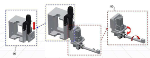
도 2는 종래 기술에 따른 반도체 제조 장치의 평면도이다.
도 3은 본 발명의 일 실시예에 따른 반도체 패키지 제조 장치의 평면도이다.
도 4는 본 발명의 다른 실시 예에 따른 반도체 장치의 평면도이다.
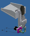
도 5는 도 1의 반도체 장치를 나타내는 사시도이다.
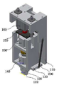
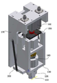
도 6은 본 발명에 따른 본딩 장치를 나타내는 사시도이다.
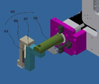
도 7은 본 발명에 따른 비젼 센서가 장착된 본딩 장치를 도시하는 사시도이다.
도 8 및 도 9는 종래 기술에 따른 플립퍼 장치를 나타내는 사시도이다.
도 10 및 도 11은 본 발명의 일 실시예에 따른 플립퍼의 구성을 나타내는 사시도이다.
도 12는 본 발명의 다른 실시예에 따른 플립퍼의 구성을 나타내는 사시도이다.
Claims (4)
- 슬라이딩 축에 연결되어 평행 이동 가능한 반도체 제조 장치의 플립퍼로서,
상기 플립퍼는 상기 슬라이딩 축에 직교하는 고정축 상에 배치되고, 상기 고정축 상에 배치된 플립 헤드를 구비하며,
상기 플립 헤드는 상기 고정축과 직교하는 암과, 상기 암에 직교하는 픽업부를 갖고,
상기 플립퍼는 상기 슬라이딩 축을 따라 평행 이동하는 동작과, 상기 플립 헤드를 180도 회전시켜 반도체 칩을 뒤집는 동작을 동시에 수행할 수 있는 반도체 제조 장치의 플립퍼.
- 제 1 항에 있어서,
상기 픽업부는 상기 고정축과 평행하게 배치되는 반도체 제조 장치의 플립퍼.
- 제 1 항에 있어서,
상기 플립퍼는 하나의 익스펜딩 스테이지와 본딩 장치를 수평 이동 가능하게 구성된 반도체 제조 장치의 플립퍼.
- 제 1 항에 있어서,
상기 플립퍼는 하나의 반도체 제조 장치에 두 개로 구성되는 반도체 제조 장치의 플립퍼.
Priority Applications (1)
| Application Number | Priority Date | Filing Date | Title |
|---|---|---|---|
| KR1020170025874A KR101944355B1 (ko) | 2017-02-28 | 2017-02-28 | 반도체 제조 장치 |
Applications Claiming Priority (1)
| Application Number | Priority Date | Filing Date | Title |
|---|---|---|---|
| KR1020170025874A KR101944355B1 (ko) | 2017-02-28 | 2017-02-28 | 반도체 제조 장치 |
Publications (2)
| Publication Number | Publication Date |
|---|---|
| KR20180098987A true KR20180098987A (ko) | 2018-09-05 |
| KR101944355B1 KR101944355B1 (ko) | 2019-01-31 |
Family
ID=63594758
Family Applications (1)
| Application Number | Title | Priority Date | Filing Date |
|---|---|---|---|
| KR1020170025874A Expired - Fee Related KR101944355B1 (ko) | 2017-02-28 | 2017-02-28 | 반도체 제조 장치 |
Country Status (1)
| Country | Link |
|---|---|
| KR (1) | KR101944355B1 (ko) |
Cited By (1)
| Publication number | Priority date | Publication date | Assignee | Title |
|---|---|---|---|---|
| CN111128771A (zh) * | 2019-12-19 | 2020-05-08 | 西北电子装备技术研究所(中国电子科技集团公司第二研究所) | 芯片基板大压力倒装键合调平台的自调平及锁定方法 |
Citations (3)
| Publication number | Priority date | Publication date | Assignee | Title |
|---|---|---|---|---|
| JP2006310480A (ja) * | 2005-04-27 | 2006-11-09 | Toshiba Corp | 半導体装置の製造装置および製造方法 |
| KR20080068876A (ko) * | 2005-12-22 | 2008-07-24 | 시바우라 메카트로닉스 가부시키가이샤 | 전자 부품의 실장 장치 및 실장 방법 |
| KR20110105535A (ko) * | 2010-03-19 | 2011-09-27 | 아메스산업(주) | 비전카메라 일체형 픽업유닛을 구비하는 플립칩 장착 장치 |
-
2017
- 2017-02-28 KR KR1020170025874A patent/KR101944355B1/ko not_active Expired - Fee Related
Patent Citations (3)
| Publication number | Priority date | Publication date | Assignee | Title |
|---|---|---|---|---|
| JP2006310480A (ja) * | 2005-04-27 | 2006-11-09 | Toshiba Corp | 半導体装置の製造装置および製造方法 |
| KR20080068876A (ko) * | 2005-12-22 | 2008-07-24 | 시바우라 메카트로닉스 가부시키가이샤 | 전자 부품의 실장 장치 및 실장 방법 |
| KR20110105535A (ko) * | 2010-03-19 | 2011-09-27 | 아메스산업(주) | 비전카메라 일체형 픽업유닛을 구비하는 플립칩 장착 장치 |
Cited By (1)
| Publication number | Priority date | Publication date | Assignee | Title |
|---|---|---|---|---|
| CN111128771A (zh) * | 2019-12-19 | 2020-05-08 | 西北电子装备技术研究所(中国电子科技集团公司第二研究所) | 芯片基板大压力倒装键合调平台的自调平及锁定方法 |
Also Published As
| Publication number | Publication date |
|---|---|
| KR101944355B1 (ko) | 2019-01-31 |
Similar Documents
| Publication | Publication Date | Title |
|---|---|---|
| US10896902B2 (en) | Systems and methods for efficient transfer of semiconductor elements | |
| CN107180772B (zh) | 芯片贴装装置以及半导体器件的制造方法 | |
| US12136563B2 (en) | Semiconductor manufacturing apparatus including bonding head | |
| KR102330577B1 (ko) | 전자 부품의 픽업 장치 및 실장 장치 | |
| KR102003130B1 (ko) | 반도체 제조 장치 및 반도체 장치의 제조 방법 | |
| KR20170042955A (ko) | 다이 본딩 장치 | |
| JP2009194306A (ja) | 部品供給装置 | |
| KR101605077B1 (ko) | 웨이퍼 상에 칩을 정밀하게 본딩하기 위한 장치 | |
| KR20170042957A (ko) | 반도체 다이들을 이송하기 위한 다이 셔틀 및 이를 포함하는 다이 본딩 장치 | |
| KR101944355B1 (ko) | 반도체 제조 장치 | |
| KR101939347B1 (ko) | 반도체 제조 장치 | |
| KR101946851B1 (ko) | 반도체 제조 장치 | |
| JP6847206B2 (ja) | ユニバーサルチップバッチボンディング装置及び方法 | |
| KR101794978B1 (ko) | 반도체 제조 장치의 플립퍼 | |
| KR101946843B1 (ko) | 반도체 제조 장치 | |
| KR102536175B1 (ko) | 다이 본딩 장치 | |
| KR101939343B1 (ko) | 반도체 제조 장치 | |
| KR101649073B1 (ko) | 반도체 패키지 제조를 위한 본딩 장치 | |
| US20240186174A1 (en) | Apparatus for manufacturing semiconductor devices and method of manufacturing semiconductor devices | |
| KR20170113773A (ko) | 반도체 패키지 제조를 위한 본딩 장치 | |
| KR101794977B1 (ko) | 반도체 제조 장치 | |
| KR101685910B1 (ko) | 반도체 패키지 제조 방법 | |
| KR20180083742A (ko) | 플립소자 핸들러 | |
| US20250385109A1 (en) | Semiconductor manufacturing apparatus including bonding head | |
| US10438922B2 (en) | Method and system for mounting components in semiconductor fabrication process |
Legal Events
| Date | Code | Title | Description |
|---|---|---|---|
| A201 | Request for examination | ||
| PA0109 | Patent application |
St.27 status event code: A-0-1-A10-A12-nap-PA0109 |
|
| PA0201 | Request for examination |
St.27 status event code: A-1-2-D10-D11-exm-PA0201 |
|
| D13-X000 | Search requested |
St.27 status event code: A-1-2-D10-D13-srh-X000 |
|
| D14-X000 | Search report completed |
St.27 status event code: A-1-2-D10-D14-srh-X000 |
|
| E902 | Notification of reason for refusal | ||
| PE0902 | Notice of grounds for rejection |
St.27 status event code: A-1-2-D10-D21-exm-PE0902 |
|
| E13-X000 | Pre-grant limitation requested |
St.27 status event code: A-2-3-E10-E13-lim-X000 |
|
| P11-X000 | Amendment of application requested |
St.27 status event code: A-2-2-P10-P11-nap-X000 |
|
| P13-X000 | Application amended |
St.27 status event code: A-2-2-P10-P13-nap-X000 |
|
| PG1501 | Laying open of application |
St.27 status event code: A-1-1-Q10-Q12-nap-PG1501 |
|
| E701 | Decision to grant or registration of patent right | ||
| PE0701 | Decision of registration |
St.27 status event code: A-1-2-D10-D22-exm-PE0701 |
|
| GRNT | Written decision to grant | ||
| PR0701 | Registration of establishment |
St.27 status event code: A-2-4-F10-F11-exm-PR0701 |
|
| PR1002 | Payment of registration fee |
St.27 status event code: A-2-2-U10-U11-oth-PR1002 Fee payment year number: 1 |
|
| PG1601 | Publication of registration |
St.27 status event code: A-4-4-Q10-Q13-nap-PG1601 |
|
| P14-X000 | Amendment of ip right document requested |
St.27 status event code: A-5-5-P10-P14-nap-X000 |
|
| R18-X000 | Changes to party contact information recorded |
St.27 status event code: A-5-5-R10-R18-oth-X000 |
|
| LAPS | Lapse due to unpaid annual fee | ||
| PC1903 | Unpaid annual fee |
St.27 status event code: A-4-4-U10-U13-oth-PC1903 Not in force date: 20220126 Payment event data comment text: Termination Category : DEFAULT_OF_REGISTRATION_FEE |
|
| PC1903 | Unpaid annual fee |
St.27 status event code: N-4-6-H10-H13-oth-PC1903 Ip right cessation event data comment text: Termination Category : DEFAULT_OF_REGISTRATION_FEE Not in force date: 20220126 |
|
| P22-X000 | Classification modified |
St.27 status event code: A-4-4-P10-P22-nap-X000 |
|
| P22-X000 | Classification modified |
St.27 status event code: A-4-4-P10-P22-nap-X000 |