KR20180098138A - 기존 토포그래피 위에 평탄화된 에칭 마스크 구조를 형성하는 방법 - Google Patents
기존 토포그래피 위에 평탄화된 에칭 마스크 구조를 형성하는 방법 Download PDFInfo
- Publication number
- KR20180098138A KR20180098138A KR1020180017407A KR20180017407A KR20180098138A KR 20180098138 A KR20180098138 A KR 20180098138A KR 1020180017407 A KR1020180017407 A KR 1020180017407A KR 20180017407 A KR20180017407 A KR 20180017407A KR 20180098138 A KR20180098138 A KR 20180098138A
- Authority
- KR
- South Korea
- Prior art keywords
- layer
- feature
- substrate
- stack
- features
- Prior art date
- Legal status (The legal status is an assumption and is not a legal conclusion. Google has not performed a legal analysis and makes no representation as to the accuracy of the status listed.)
- Granted
Links
Images


Classifications
-
- H01L21/0337—
-
- H—ELECTRICITY
- H10—SEMICONDUCTOR DEVICES; ELECTRIC SOLID-STATE DEVICES NOT OTHERWISE PROVIDED FOR
- H10P—GENERIC PROCESSES OR APPARATUS FOR THE MANUFACTURE OR TREATMENT OF DEVICES COVERED BY CLASS H10
- H10P76/00—Manufacture or treatment of masks on semiconductor bodies, e.g. by lithography or photolithography
- H10P76/40—Manufacture or treatment of masks on semiconductor bodies, e.g. by lithography or photolithography of masks comprising inorganic materials
- H10P76/408—Manufacture or treatment of masks on semiconductor bodies, e.g. by lithography or photolithography of masks comprising inorganic materials characterised by their sizes, orientations, dispositions, behaviours or shapes
- H10P76/4085—Manufacture or treatment of masks on semiconductor bodies, e.g. by lithography or photolithography of masks comprising inorganic materials characterised by their sizes, orientations, dispositions, behaviours or shapes characterised by the processes involved to create the masks
-
- H—ELECTRICITY
- H10—SEMICONDUCTOR DEVICES; ELECTRIC SOLID-STATE DEVICES NOT OTHERWISE PROVIDED FOR
- H10P—GENERIC PROCESSES OR APPARATUS FOR THE MANUFACTURE OR TREATMENT OF DEVICES COVERED BY CLASS H10
- H10P50/00—Etching of wafers, substrates or parts of devices
- H10P50/69—Etching of wafers, substrates or parts of devices using masks for semiconductor materials
- H10P50/691—Etching of wafers, substrates or parts of devices using masks for semiconductor materials for Group V materials or Group III-V materials
- H10P50/692—Etching of wafers, substrates or parts of devices using masks for semiconductor materials for Group V materials or Group III-V materials characterised by their composition, e.g. multilayer masks or materials
-
- G—PHYSICS
- G03—PHOTOGRAPHY; CINEMATOGRAPHY; ANALOGOUS TECHNIQUES USING WAVES OTHER THAN OPTICAL WAVES; ELECTROGRAPHY; HOLOGRAPHY
- G03F—PHOTOMECHANICAL PRODUCTION OF TEXTURED OR PATTERNED SURFACES, e.g. FOR PRINTING, FOR PROCESSING OF SEMICONDUCTOR DEVICES; MATERIALS THEREFOR; ORIGINALS THEREFOR; APPARATUS SPECIALLY ADAPTED THEREFOR
- G03F7/00—Photomechanical, e.g. photolithographic, production of textured or patterned surfaces, e.g. printing surfaces; Materials therefor, e.g. comprising photoresists; Apparatus specially adapted therefor
- G03F7/0002—Lithographic processes using patterning methods other than those involving the exposure to radiation, e.g. by stamping
-
- H01L21/0274—
-
- H01L21/76816—
-
- H—ELECTRICITY
- H10—SEMICONDUCTOR DEVICES; ELECTRIC SOLID-STATE DEVICES NOT OTHERWISE PROVIDED FOR
- H10P—GENERIC PROCESSES OR APPARATUS FOR THE MANUFACTURE OR TREATMENT OF DEVICES COVERED BY CLASS H10
- H10P14/00—Formation of materials, e.g. in the shape of layers or pillars
- H10P14/60—Formation of materials, e.g. in the shape of layers or pillars of insulating materials
- H10P14/63—Formation of materials, e.g. in the shape of layers or pillars of insulating materials characterised by the formation processes
- H10P14/6326—Deposition processes
- H10P14/6342—Liquid deposition, e.g. spin-coating, sol-gel techniques or spray coating
-
- H—ELECTRICITY
- H10—SEMICONDUCTOR DEVICES; ELECTRIC SOLID-STATE DEVICES NOT OTHERWISE PROVIDED FOR
- H10P—GENERIC PROCESSES OR APPARATUS FOR THE MANUFACTURE OR TREATMENT OF DEVICES COVERED BY CLASS H10
- H10P14/00—Formation of materials, e.g. in the shape of layers or pillars
- H10P14/60—Formation of materials, e.g. in the shape of layers or pillars of insulating materials
- H10P14/69—Inorganic materials
- H10P14/6902—Inorganic materials composed of carbon, e.g. alpha-C, diamond or hydrogen doped carbon
-
- H—ELECTRICITY
- H10—SEMICONDUCTOR DEVICES; ELECTRIC SOLID-STATE DEVICES NOT OTHERWISE PROVIDED FOR
- H10P—GENERIC PROCESSES OR APPARATUS FOR THE MANUFACTURE OR TREATMENT OF DEVICES COVERED BY CLASS H10
- H10P50/00—Etching of wafers, substrates or parts of devices
- H10P50/20—Dry etching; Plasma etching; Reactive-ion etching
- H10P50/28—Dry etching; Plasma etching; Reactive-ion etching of insulating materials
- H10P50/282—Dry etching; Plasma etching; Reactive-ion etching of insulating materials of inorganic materials
- H10P50/283—Dry etching; Plasma etching; Reactive-ion etching of insulating materials of inorganic materials by chemical means
-
- H—ELECTRICITY
- H10—SEMICONDUCTOR DEVICES; ELECTRIC SOLID-STATE DEVICES NOT OTHERWISE PROVIDED FOR
- H10P—GENERIC PROCESSES OR APPARATUS FOR THE MANUFACTURE OR TREATMENT OF DEVICES COVERED BY CLASS H10
- H10P50/00—Etching of wafers, substrates or parts of devices
- H10P50/69—Etching of wafers, substrates or parts of devices using masks for semiconductor materials
- H10P50/691—Etching of wafers, substrates or parts of devices using masks for semiconductor materials for Group V materials or Group III-V materials
- H10P50/693—Etching of wafers, substrates or parts of devices using masks for semiconductor materials for Group V materials or Group III-V materials characterised by their size, orientation, disposition, behaviour or shape, in horizontal or vertical plane
- H10P50/695—Etching of wafers, substrates or parts of devices using masks for semiconductor materials for Group V materials or Group III-V materials characterised by their size, orientation, disposition, behaviour or shape, in horizontal or vertical plane characterised by the process involved to create the mask, e.g. lift-off masks or sidewalls or to modify the mask
-
- H—ELECTRICITY
- H10—SEMICONDUCTOR DEVICES; ELECTRIC SOLID-STATE DEVICES NOT OTHERWISE PROVIDED FOR
- H10P—GENERIC PROCESSES OR APPARATUS FOR THE MANUFACTURE OR TREATMENT OF DEVICES COVERED BY CLASS H10
- H10P50/00—Etching of wafers, substrates or parts of devices
- H10P50/69—Etching of wafers, substrates or parts of devices using masks for semiconductor materials
- H10P50/691—Etching of wafers, substrates or parts of devices using masks for semiconductor materials for Group V materials or Group III-V materials
- H10P50/693—Etching of wafers, substrates or parts of devices using masks for semiconductor materials for Group V materials or Group III-V materials characterised by their size, orientation, disposition, behaviour or shape, in horizontal or vertical plane
- H10P50/696—Process specially adapted to improve the resolution of the mask
-
- H—ELECTRICITY
- H10—SEMICONDUCTOR DEVICES; ELECTRIC SOLID-STATE DEVICES NOT OTHERWISE PROVIDED FOR
- H10P—GENERIC PROCESSES OR APPARATUS FOR THE MANUFACTURE OR TREATMENT OF DEVICES COVERED BY CLASS H10
- H10P76/00—Manufacture or treatment of masks on semiconductor bodies, e.g. by lithography or photolithography
- H10P76/20—Manufacture or treatment of masks on semiconductor bodies, e.g. by lithography or photolithography of masks comprising organic materials
- H10P76/204—Manufacture or treatment of masks on semiconductor bodies, e.g. by lithography or photolithography of masks comprising organic materials of organic photoresist masks
- H10P76/2041—Photolithographic processes
-
- H—ELECTRICITY
- H10—SEMICONDUCTOR DEVICES; ELECTRIC SOLID-STATE DEVICES NOT OTHERWISE PROVIDED FOR
- H10P—GENERIC PROCESSES OR APPARATUS FOR THE MANUFACTURE OR TREATMENT OF DEVICES COVERED BY CLASS H10
- H10P76/00—Manufacture or treatment of masks on semiconductor bodies, e.g. by lithography or photolithography
- H10P76/40—Manufacture or treatment of masks on semiconductor bodies, e.g. by lithography or photolithography of masks comprising inorganic materials
- H10P76/405—Manufacture or treatment of masks on semiconductor bodies, e.g. by lithography or photolithography of masks comprising inorganic materials characterised by their composition, e.g. multilayer masks
-
- H—ELECTRICITY
- H10—SEMICONDUCTOR DEVICES; ELECTRIC SOLID-STATE DEVICES NOT OTHERWISE PROVIDED FOR
- H10P—GENERIC PROCESSES OR APPARATUS FOR THE MANUFACTURE OR TREATMENT OF DEVICES COVERED BY CLASS H10
- H10P95/00—Generic processes or apparatus for manufacture or treatments not covered by the other groups of this subclass
- H10P95/06—Planarisation of inorganic insulating materials
-
- H—ELECTRICITY
- H10—SEMICONDUCTOR DEVICES; ELECTRIC SOLID-STATE DEVICES NOT OTHERWISE PROVIDED FOR
- H10W—GENERIC PACKAGES, INTERCONNECTIONS, CONNECTORS OR OTHER CONSTRUCTIONAL DETAILS OF DEVICES COVERED BY CLASS H10
- H10W20/00—Interconnections in chips, wafers or substrates
- H10W20/01—Manufacture or treatment
- H10W20/071—Manufacture or treatment of dielectric parts thereof
- H10W20/081—Manufacture or treatment of dielectric parts thereof by forming openings in the dielectric parts
- H10W20/089—Manufacture or treatment of dielectric parts thereof by forming openings in the dielectric parts using processes for implementing desired shapes or dispositions of the openings, e.g. double patterning
Landscapes
- Physics & Mathematics (AREA)
- General Physics & Mathematics (AREA)
- Drying Of Semiconductors (AREA)
- Exposure Of Semiconductors, Excluding Electron Or Ion Beam Exposure (AREA)
- Laminated Bodies (AREA)
- Chemical & Material Sciences (AREA)
- Chemical Kinetics & Catalysis (AREA)
- General Chemical & Material Sciences (AREA)
- Shaping Of Tube Ends By Bending Or Straightening (AREA)
Abstract
Description
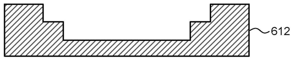
도 2는 고화된 패터닝된 층이 그 위에 형성된, 도 1에 도시된 기판의 단순화된 도면.
도 3은 도 2의 것과 유사한 패터닝된 층의 100nm 미만 피쳐의 기계적 강성도(영 모듈러스)의 단순화된 플롯.
도 4는 피쳐 종횡비의 함수로서 100nm 미만 피쳐를 지지하는데 필요한 기계적 강성도(영 모듈러스)의 단순화된 플롯.
또한, 도 5a 내지 도 5h는 다층 레지스트 스택 내로 그리고 그후 기판 내로의 패턴 전사 시퀀스의 단순화된 도면.
또한, 도 6a 내지 도 6i는 본 발명의 일 실시예에 따른 다층 레지스트 스택 내로의 그리고 그후 기판으로의 패턴 전사 시퀀스의 단순화된 도면.
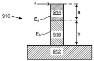
도 7은 도 6g에 도시된 것과 유사한 다층 레지스트 스택에 형성된 피쳐의 단순화된 도면.
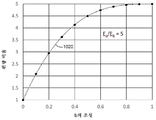
도 8은 그 재료 조성의 함수로서 도 7의 피쳐와 유사한 피쳐의 편향 비율의 단순화된 플롯.
도 9는 상이한 다층 레지스트 스택에 형성된 피쳐의 단순화된 도면.
도 10은 그 재료 조성의 함수로서의 도 9의 피쳐의 편향의 단순화된 플롯.


Claims (13)
- 비-평면(non-planar) 표면 변화가 있는 표면을 갖는 기판을 제공하는 단계;
상기 기판 위에 제1 기저층을 부착하는 단계로서, 형성되는 상기 제1 기저층이 아래에 있는 상기 기판의 비-평면 표면 변화에 대응하는 비평면 표면 변화를 갖는, 제1 기저층을 부착하는 단계, 및
상기 제1 기저층 위에 제2 평탄화층을 부착하는 단계
에 의해, 상기 기판 상에 다층 스택을 형성하는 단계;
상기 다층 스택 상에 하드 마스크를 피착하는 단계; 및
상기 하드 마스크 상에 패터닝된 층을 형성하는 단계를 포함하고,
형성된 상기 패터닝된 층은 피쳐(features)를 갖고,
상기 다층 스택은, 50nm 이하의 피쳐 치수 및 2.5:1 이상의 종횡비를 갖는 하나 이상의 에칭된 피쳐를 최소 피쳐 압궤(collapse)로 유지하는 데 충분한 복합 유효 기계적 강성도(Eeff)를 갖는, 방법. - 제1항에 있어서, 상기 하나 이상의 에칭된 피쳐는 5:1 이상의 종횡비를 갖는, 방법.
- 제1항에 있어서, 상기 다층 스택의 하나 이상의 에칭된 피쳐의 피쳐 압궤는, 동일한 조건 하에서 전체적으로 제2 평탄화 재료로 형성된 층으로 에칭된 동일한 피쳐와 비교하여 감소되는, 방법.
- 제3항에 있어서, 제2 평탄화 재료의 에칭 내성은 상기 제1 기저층의 에칭 내성의 30 % 이내인, 방법.
- 제1항에 있어서, 상기 패터닝된 층의 피쳐는 특정 임계 치수(CD)를 가지며, 상기 다층 스택의 에칭된 피쳐는 전체적으로 제1 기저층 재료로 형성된 층으로 에칭된 동일한 피쳐와 비교하여 더 높은 임계 치수(CD) 균일성을 유지하는, 방법.
- 제1항에 있어서, 상기 다층 스택은 피쳐 압궤없이 상기 하나 이상의 에칭된 피쳐를 유지하는 데 충분한 복합 유효 기계적 강성도(Eeff)를 가지는, 방법.
- 제1항 내지 제6항 중 어느 한 항에 있어서, 상기 형성된 패터닝된 층의 피쳐를 상기 다층 스택으로 에칭하는 하나 이상의 에칭 단계를 수행하는 단계를 더 포함하는, 방법.
- 제7항에 있어서, 상기 형성된 패터닝된 층의 피쳐를 상기 기판으로 전사하기 위해 하나 이상의 추가 에칭 단계를 수행하는 단계를 더 포함하는, 방법.
- 다층 스택이며,
비-평면 표면 변화가 있는 표면을 갖는 기판;
상기 기판의 표면 위에 형성되고, 상기 기판 표면의 비-평면 표면 변화에 대응하는 비-평면 표면 변화를 갖는 제1 탄소 층; 및
상기 제1 탄소 층 위에 형성되고 평면 표면을 갖는 제2 평탄화 층을 포함하며,
다층 스택은 2.5:1 이상의 종횡비에서 50nm 이하의 피쳐를 최소 피쳐 압궤로 유지하는 데 충분한 복합 유효 기계적 강성도(Eeff)를 갖는, 다층 스택. - 제9항에 있어서, 상기 다층 스택은, 5:1 이상의 종횡비에서 50nm 이하의 피쳐를 최소 피쳐 압궤로 유지하는 데 충분한 복합 유효 기계적 강성도(Eeff)를 갖는, 다층 스택.
- 제9항에 있어서, 상기 제2 평탄화 층의 에칭 내성은 제1 탄소 층의 에칭 내성의 30 % 이내인, 다층 스택.
- 디바이스를 제조하는 방법이며,
제8항의 방법에 따라 형성된 패터닝된 층의 피쳐를 기판으로 전사하는 단계, 및
상기 기판을 처리하여 디바이스를 제조하는 단계를 포함하는, 방법. - 제12항에 있어서, 상기 기판은 반도체 웨이퍼를 더 포함하며, 제조된 상기 디바이스는 반도체 디바이스인, 방법.
Applications Claiming Priority (2)
| Application Number | Priority Date | Filing Date | Title |
|---|---|---|---|
| US15/441,381 US10079152B1 (en) | 2017-02-24 | 2017-02-24 | Method for forming planarized etch mask structures over existing topography |
| US15/441,381 | 2017-02-24 |
Publications (2)
| Publication Number | Publication Date |
|---|---|
| KR20180098138A true KR20180098138A (ko) | 2018-09-03 |
| KR102253295B1 KR102253295B1 (ko) | 2021-05-20 |
Family
ID=63246983
Family Applications (1)
| Application Number | Title | Priority Date | Filing Date |
|---|---|---|---|
| KR1020180017407A Active KR102253295B1 (ko) | 2017-02-24 | 2018-02-13 | 기존 토포그래피 위에 평탄화된 에칭 마스크 구조를 형성하는 방법 |
Country Status (3)
| Country | Link |
|---|---|
| US (1) | US10079152B1 (ko) |
| JP (1) | JP7222606B2 (ko) |
| KR (1) | KR102253295B1 (ko) |
Cited By (1)
| Publication number | Priority date | Publication date | Assignee | Title |
|---|---|---|---|---|
| KR20210080218A (ko) * | 2019-12-20 | 2021-06-30 | 캐논 가부시끼가이샤 | 임프린트 시스템 내의 왜곡의 보정을 갖는 나노제조 방법 |
Families Citing this family (6)
| Publication number | Priority date | Publication date | Assignee | Title |
|---|---|---|---|---|
| JP7403961B2 (ja) * | 2019-03-19 | 2023-12-25 | キオクシア株式会社 | インプリント方法および半導体装置の製造方法 |
| JP7336303B2 (ja) * | 2019-07-31 | 2023-08-31 | キヤノン株式会社 | 物品製造方法、膜形成方法、型製造方法、物品製造システム、情報処理方法およびプログラム |
| US11656546B2 (en) | 2020-02-27 | 2023-05-23 | Canon Kabushiki Kaisha | Exposure apparatus for uniform light intensity and methods of using the same |
| US11349061B2 (en) * | 2020-06-08 | 2022-05-31 | International Business Machines Corporation | Glassy carbon mask for immersion implant and selective laser anneal |
| US11443940B2 (en) * | 2020-06-24 | 2022-09-13 | Canon Kabushiki Kaisha | Apparatus for uniform light intensity and methods of using the same |
| US20250013153A1 (en) * | 2023-07-06 | 2025-01-09 | Tokyo Electron Limited | Method of preventing pattern collapse |
Citations (4)
| Publication number | Priority date | Publication date | Assignee | Title |
|---|---|---|---|---|
| US20050184637A1 (en) * | 2004-01-29 | 2005-08-25 | Asahi Glass Company, Limited | Envelope for a flat panel display and flat panel display employing the envelope |
| US20130068720A1 (en) * | 2011-09-16 | 2013-03-21 | Shuichi Taniguchi | Pattern forming method |
| US20140227887A1 (en) * | 2011-09-06 | 2014-08-14 | Dongjin Semichem Co., Ltd. | Phenol-based self-crosslinking polymer and resist underlayer film composition including same |
| US20170003568A1 (en) * | 2014-01-30 | 2017-01-05 | Sony Corporation | Display unit and electronic apparatus |
Family Cites Families (15)
| Publication number | Priority date | Publication date | Assignee | Title |
|---|---|---|---|---|
| US6873087B1 (en) | 1999-10-29 | 2005-03-29 | Board Of Regents, The University Of Texas System | High precision orientation alignment and gap control stages for imprint lithography processes |
| US7077992B2 (en) | 2002-07-11 | 2006-07-18 | Molecular Imprints, Inc. | Step and repeat imprint lithography processes |
| US6932934B2 (en) | 2002-07-11 | 2005-08-23 | Molecular Imprints, Inc. | Formation of discontinuous films during an imprint lithography process |
| US7179396B2 (en) | 2003-03-25 | 2007-02-20 | Molecular Imprints, Inc. | Positive tone bi-layer imprint lithography method |
| US7396475B2 (en) | 2003-04-25 | 2008-07-08 | Molecular Imprints, Inc. | Method of forming stepped structures employing imprint lithography |
| US7157036B2 (en) | 2003-06-17 | 2007-01-02 | Molecular Imprints, Inc | Method to reduce adhesion between a conformable region and a pattern of a mold |
| US7790231B2 (en) | 2003-07-10 | 2010-09-07 | Brewer Science Inc. | Automated process and apparatus for planarization of topographical surfaces |
| US8076386B2 (en) | 2004-02-23 | 2011-12-13 | Molecular Imprints, Inc. | Materials for imprint lithography |
| US7998651B2 (en) | 2006-05-15 | 2011-08-16 | Asml Netherlands B.V. | Imprint lithography |
| US11392037B2 (en) | 2008-02-18 | 2022-07-19 | Nissan Chemical Industries, Ltd. | Resist underlayer film forming composition containing silicone having cyclic amino group |
| US8071275B2 (en) | 2008-04-10 | 2011-12-06 | Lexmark International, Inc. | Methods for planarizing unevenness on surface of wafer photoresist layer and wafers produced by the methods |
| KR101653195B1 (ko) | 2008-06-09 | 2016-09-01 | 보드 오브 리전츠 더 유니버시티 오브 텍사스 시스템 | 적응적 나노토포그래피 형상제작 |
| CN104137235B (zh) | 2012-01-19 | 2017-02-22 | 布鲁尔科技公司 | 含金刚烷基的非聚合物减反射组合物 |
| KR102292465B1 (ko) | 2013-08-19 | 2021-08-20 | 보드 오브 레젼츠, 더 유니버시티 오브 텍사스 시스템 | 나노미터 스케일 정확도를 갖는 사용자 정의 프로파일의 프로그램 가능한 박막 적층 방법 |
| WO2015037398A1 (ja) | 2013-09-11 | 2015-03-19 | Jsr株式会社 | 多層レジストプロセス用無機膜形成組成物及びパターン形成方法 |
-
2017
- 2017-02-24 US US15/441,381 patent/US10079152B1/en active Active
-
2018
- 2018-02-13 KR KR1020180017407A patent/KR102253295B1/ko active Active
- 2018-02-19 JP JP2018027233A patent/JP7222606B2/ja active Active
Patent Citations (5)
| Publication number | Priority date | Publication date | Assignee | Title |
|---|---|---|---|---|
| US20050184637A1 (en) * | 2004-01-29 | 2005-08-25 | Asahi Glass Company, Limited | Envelope for a flat panel display and flat panel display employing the envelope |
| US20140227887A1 (en) * | 2011-09-06 | 2014-08-14 | Dongjin Semichem Co., Ltd. | Phenol-based self-crosslinking polymer and resist underlayer film composition including same |
| US20130068720A1 (en) * | 2011-09-16 | 2013-03-21 | Shuichi Taniguchi | Pattern forming method |
| JP2013065725A (ja) * | 2011-09-16 | 2013-04-11 | Toshiba Corp | パターン形成方法 |
| US20170003568A1 (en) * | 2014-01-30 | 2017-01-05 | Sony Corporation | Display unit and electronic apparatus |
Cited By (1)
| Publication number | Priority date | Publication date | Assignee | Title |
|---|---|---|---|---|
| KR20210080218A (ko) * | 2019-12-20 | 2021-06-30 | 캐논 가부시끼가이샤 | 임프린트 시스템 내의 왜곡의 보정을 갖는 나노제조 방법 |
Also Published As
| Publication number | Publication date |
|---|---|
| KR102253295B1 (ko) | 2021-05-20 |
| JP2018142701A (ja) | 2018-09-13 |
| JP7222606B2 (ja) | 2023-02-15 |
| US20180247823A1 (en) | 2018-08-30 |
| US10079152B1 (en) | 2018-09-18 |
Similar Documents
| Publication | Publication Date | Title |
|---|---|---|
| KR102253295B1 (ko) | 기존 토포그래피 위에 평탄화된 에칭 마스크 구조를 형성하는 방법 | |
| US8012394B2 (en) | Template pattern density doubling | |
| US7960090B2 (en) | Pattern forming method, pattern formed thereby, mold, processing apparatus, and processing method | |
| US8961852B2 (en) | Templates having high contrast alignment marks | |
| US7140861B2 (en) | Compliant hard template for UV imprinting | |
| US7357876B2 (en) | Eliminating printability of sub-resolution defects in imprint lithography | |
| JP5404654B2 (ja) | テンプレート形成時の限界寸法制御 | |
| US10211051B2 (en) | Method of reverse tone patterning | |
| CN108020986B (zh) | 从形成在衬底上的固化图案层分离纳米压印模板的设备和方法 | |
| KR102379626B1 (ko) | 차광 재료를 구비한 나노임프린트 템플릿 및 제작 방법 | |
| JP2009182075A (ja) | インプリントによる構造体の製造方法 | |
| CN114097062B (zh) | 用于调整衬底上膜的应力过渡的方法 | |
| US8935981B2 (en) | High contrast alignment marks through multiple stage imprinting | |
| US7985530B2 (en) | Etch-enhanced technique for lift-off patterning | |
| JP5848386B2 (ja) | インサイチュ嵌込み構造物形成方法 | |
| US20100095862A1 (en) | Double Sidewall Angle Nano-Imprint Template | |
| KR20210080218A (ko) | 임프린트 시스템 내의 왜곡의 보정을 갖는 나노제조 방법 | |
| KR20220034874A (ko) | 스핀-온 및 cvd 증착된 유기 막의 평탄화를 위한 방법 | |
| TW202400507A (zh) | 用於製造壓印微影模板的方法、用於製造光學部件的方法以及用於製造光學元件的方法 | |
| US12085852B2 (en) | Template, method of forming a template, apparatus and method of manufacturing an article |
Legal Events
| Date | Code | Title | Description |
|---|---|---|---|
| PA0109 | Patent application |
St.27 status event code: A-0-1-A10-A12-nap-PA0109 |
|
| PG1501 | Laying open of application |
St.27 status event code: A-1-1-Q10-Q12-nap-PG1501 |
|
| A201 | Request for examination | ||
| PA0201 | Request for examination |
St.27 status event code: A-1-2-D10-D11-exm-PA0201 |
|
| E902 | Notification of reason for refusal | ||
| PE0902 | Notice of grounds for rejection |
St.27 status event code: A-1-2-D10-D21-exm-PE0902 |
|
| E13-X000 | Pre-grant limitation requested |
St.27 status event code: A-2-3-E10-E13-lim-X000 |
|
| P11-X000 | Amendment of application requested |
St.27 status event code: A-2-2-P10-P11-nap-X000 |
|
| P13-X000 | Application amended |
St.27 status event code: A-2-2-P10-P13-nap-X000 |
|
| E701 | Decision to grant or registration of patent right | ||
| PE0701 | Decision of registration |
St.27 status event code: A-1-2-D10-D22-exm-PE0701 |
|
| GRNT | Written decision to grant | ||
| PR0701 | Registration of establishment |
St.27 status event code: A-2-4-F10-F11-exm-PR0701 |
|
| PR1002 | Payment of registration fee |
St.27 status event code: A-2-2-U10-U11-oth-PR1002 Fee payment year number: 1 |
|
| PG1601 | Publication of registration |
St.27 status event code: A-4-4-Q10-Q13-nap-PG1601 |
|
| PR1001 | Payment of annual fee |
St.27 status event code: A-4-4-U10-U11-oth-PR1001 Fee payment year number: 4 |
|
| P22-X000 | Classification modified |
St.27 status event code: A-4-4-P10-P22-nap-X000 |