KR20170118503A - Coil Electronic Component - Google Patents
Coil Electronic Component Download PDFInfo
- Publication number
- KR20170118503A KR20170118503A KR1020160046375A KR20160046375A KR20170118503A KR 20170118503 A KR20170118503 A KR 20170118503A KR 1020160046375 A KR1020160046375 A KR 1020160046375A KR 20160046375 A KR20160046375 A KR 20160046375A KR 20170118503 A KR20170118503 A KR 20170118503A
- Authority
- KR
- South Korea
- Prior art keywords
- coil
- layer
- pattern
- insulating layer
- layers
- Prior art date
Links
- 230000003014 reinforcing effect Effects 0.000 claims abstract description 33
- 230000000149 penetrating effect Effects 0.000 claims abstract description 5
- 238000000034 method Methods 0.000 claims description 47
- 239000011810 insulating material Substances 0.000 claims description 8
- 229910000765 intermetallic Inorganic materials 0.000 claims description 6
- 239000010410 layer Substances 0.000 description 183
- 239000010949 copper Substances 0.000 description 16
- 230000008569 process Effects 0.000 description 16
- 239000000463 material Substances 0.000 description 12
- RYGMFSIKBFXOCR-UHFFFAOYSA-N Copper Chemical compound [Cu] RYGMFSIKBFXOCR-UHFFFAOYSA-N 0.000 description 11
- 238000004519 manufacturing process Methods 0.000 description 8
- 239000011889 copper foil Substances 0.000 description 7
- 238000007747 plating Methods 0.000 description 7
- PXHVJJICTQNCMI-UHFFFAOYSA-N Nickel Chemical compound [Ni] PXHVJJICTQNCMI-UHFFFAOYSA-N 0.000 description 6
- 229910052802 copper Inorganic materials 0.000 description 5
- 239000000945 filler Substances 0.000 description 5
- 238000010030 laminating Methods 0.000 description 5
- 239000000919 ceramic Substances 0.000 description 4
- 229920005989 resin Polymers 0.000 description 4
- 239000011347 resin Substances 0.000 description 4
- KDLHZDBZIXYQEI-UHFFFAOYSA-N Palladium Chemical compound [Pd] KDLHZDBZIXYQEI-UHFFFAOYSA-N 0.000 description 3
- 229910052751 metal Inorganic materials 0.000 description 3
- 239000002184 metal Substances 0.000 description 3
- 239000000654 additive Substances 0.000 description 2
- 230000000996 additive effect Effects 0.000 description 2
- 238000005530 etching Methods 0.000 description 2
- 238000003475 lamination Methods 0.000 description 2
- 239000007769 metal material Substances 0.000 description 2
- 230000004048 modification Effects 0.000 description 2
- 238000012986 modification Methods 0.000 description 2
- 229910052759 nickel Inorganic materials 0.000 description 2
- 238000000059 patterning Methods 0.000 description 2
- 239000010936 titanium Substances 0.000 description 2
- IJRKLHTZAIFUTB-UHFFFAOYSA-N 5-nitro-2-(2-phenylethylamino)benzoic acid Chemical compound OC(=O)C1=CC([N+]([O-])=O)=CC=C1NCCC1=CC=CC=C1 IJRKLHTZAIFUTB-UHFFFAOYSA-N 0.000 description 1
- 229910018072 Al 2 O 3 Inorganic materials 0.000 description 1
- 229910004298 SiO 2 Inorganic materials 0.000 description 1
- BQCADISMDOOEFD-UHFFFAOYSA-N Silver Chemical compound [Ag] BQCADISMDOOEFD-UHFFFAOYSA-N 0.000 description 1
- ATJFFYVFTNAWJD-UHFFFAOYSA-N Tin Chemical group [Sn] ATJFFYVFTNAWJD-UHFFFAOYSA-N 0.000 description 1
- RTAQQCXQSZGOHL-UHFFFAOYSA-N Titanium Chemical compound [Ti] RTAQQCXQSZGOHL-UHFFFAOYSA-N 0.000 description 1
- 229910052782 aluminium Inorganic materials 0.000 description 1
- XAGFODPZIPBFFR-UHFFFAOYSA-N aluminium Chemical compound [Al] XAGFODPZIPBFFR-UHFFFAOYSA-N 0.000 description 1
- 230000015556 catabolic process Effects 0.000 description 1
- 230000008859 change Effects 0.000 description 1
- 239000004020 conductor Substances 0.000 description 1
- 150000001879 copper Chemical class 0.000 description 1
- 230000008878 coupling Effects 0.000 description 1
- 238000010168 coupling process Methods 0.000 description 1
- 238000005859 coupling reaction Methods 0.000 description 1
- 238000006731 degradation reaction Methods 0.000 description 1
- 230000006866 deterioration Effects 0.000 description 1
- 238000010304 firing Methods 0.000 description 1
- 230000006872 improvement Effects 0.000 description 1
- 238000009413 insulation Methods 0.000 description 1
- 239000011229 interlayer Substances 0.000 description 1
- 238000003754 machining Methods 0.000 description 1
- 238000010899 nucleation Methods 0.000 description 1
- 239000011368 organic material Substances 0.000 description 1
- 229910052763 palladium Inorganic materials 0.000 description 1
- 230000003071 parasitic effect Effects 0.000 description 1
- 238000000206 photolithography Methods 0.000 description 1
- 239000011241 protective layer Substances 0.000 description 1
- 239000004065 semiconductor Substances 0.000 description 1
- 229910052709 silver Inorganic materials 0.000 description 1
- 239000004332 silver Substances 0.000 description 1
- 239000002356 single layer Substances 0.000 description 1
- 239000000758 substrate Substances 0.000 description 1
- 239000000454 talc Substances 0.000 description 1
- 229910052623 talc Inorganic materials 0.000 description 1
- 229920001187 thermosetting polymer Polymers 0.000 description 1
- 239000010409 thin film Substances 0.000 description 1
- 229910052719 titanium Inorganic materials 0.000 description 1
- 229910000859 α-Fe Inorganic materials 0.000 description 1
Images


Classifications
-
- H—ELECTRICITY
- H01—ELECTRIC ELEMENTS
- H01F—MAGNETS; INDUCTANCES; TRANSFORMERS; SELECTION OF MATERIALS FOR THEIR MAGNETIC PROPERTIES
- H01F27/00—Details of transformers or inductances, in general
- H01F27/28—Coils; Windings; Conductive connections
- H01F27/2804—Printed windings
-
- H—ELECTRICITY
- H01—ELECTRIC ELEMENTS
- H01F—MAGNETS; INDUCTANCES; TRANSFORMERS; SELECTION OF MATERIALS FOR THEIR MAGNETIC PROPERTIES
- H01F17/00—Fixed inductances of the signal type
- H01F17/0006—Printed inductances
- H01F17/0013—Printed inductances with stacked layers
-
- H—ELECTRICITY
- H01—ELECTRIC ELEMENTS
- H01F—MAGNETS; INDUCTANCES; TRANSFORMERS; SELECTION OF MATERIALS FOR THEIR MAGNETIC PROPERTIES
- H01F17/00—Fixed inductances of the signal type
- H01F17/04—Fixed inductances of the signal type with magnetic core
-
- H—ELECTRICITY
- H01—ELECTRIC ELEMENTS
- H01F—MAGNETS; INDUCTANCES; TRANSFORMERS; SELECTION OF MATERIALS FOR THEIR MAGNETIC PROPERTIES
- H01F27/00—Details of transformers or inductances, in general
- H01F27/28—Coils; Windings; Conductive connections
- H01F27/29—Terminals; Tapping arrangements for signal inductances
- H01F27/292—Surface mounted devices
-
- H—ELECTRICITY
- H01—ELECTRIC ELEMENTS
- H01F—MAGNETS; INDUCTANCES; TRANSFORMERS; SELECTION OF MATERIALS FOR THEIR MAGNETIC PROPERTIES
- H01F41/00—Apparatus or processes specially adapted for manufacturing or assembling magnets, inductances or transformers; Apparatus or processes specially adapted for manufacturing materials characterised by their magnetic properties
- H01F41/02—Apparatus or processes specially adapted for manufacturing or assembling magnets, inductances or transformers; Apparatus or processes specially adapted for manufacturing materials characterised by their magnetic properties for manufacturing cores, coils, or magnets
- H01F41/04—Apparatus or processes specially adapted for manufacturing or assembling magnets, inductances or transformers; Apparatus or processes specially adapted for manufacturing materials characterised by their magnetic properties for manufacturing cores, coils, or magnets for manufacturing coils
- H01F41/041—Printed circuit coils
-
- H—ELECTRICITY
- H05—ELECTRIC TECHNIQUES NOT OTHERWISE PROVIDED FOR
- H05K—PRINTED CIRCUITS; CASINGS OR CONSTRUCTIONAL DETAILS OF ELECTRIC APPARATUS; MANUFACTURE OF ASSEMBLAGES OF ELECTRICAL COMPONENTS
- H05K1/00—Printed circuits
- H05K1/02—Details
- H05K1/11—Printed elements for providing electric connections to or between printed circuits
- H05K1/115—Via connections; Lands around holes or via connections
-
- H—ELECTRICITY
- H01—ELECTRIC ELEMENTS
- H01F—MAGNETS; INDUCTANCES; TRANSFORMERS; SELECTION OF MATERIALS FOR THEIR MAGNETIC PROPERTIES
- H01F17/00—Fixed inductances of the signal type
- H01F17/0006—Printed inductances
- H01F17/0013—Printed inductances with stacked layers
- H01F2017/002—Details of via holes for interconnecting the layers
-
- H—ELECTRICITY
- H01—ELECTRIC ELEMENTS
- H01F—MAGNETS; INDUCTANCES; TRANSFORMERS; SELECTION OF MATERIALS FOR THEIR MAGNETIC PROPERTIES
- H01F27/00—Details of transformers or inductances, in general
- H01F27/28—Coils; Windings; Conductive connections
- H01F27/2804—Printed windings
- H01F2027/2809—Printed windings on stacked layers
Abstract
본 발명의 일 실시 형태에 따른 코일 전자 부품은 코일층 및 상기 코일층의 상부 및 하부 중 적어도 하나에 배치된 보강층을 포함하는 바디 및 상기 바디 외부에 형성된 외부 전극을 포함하며, 상기 코일층은 절연층, 코일 패턴 및 상기 절연층을 관통하여 상기 코일 패턴과 연결된 제1 도전성 비아를 포함하며, 상기 보강층은 상기 절연층보다 강성이 높은 구조이다.A coiled electronic component according to an embodiment of the present invention includes a body including a coil layer and a reinforcing layer disposed on at least one of upper and lower portions of the coil layer and an external electrode formed outside the body, Layer, a coil pattern, and a first conductive via penetrating the insulating layer and connected to the coil pattern, wherein the reinforcing layer has a higher rigidity than the insulating layer.
Description
본 발명은 코일 전자 부품에 관한 것이다.
The present invention relates to a coil electronic component.
코일 전자 부품에 해당하는 인덕터는 저항(resistor), 컨덴서(condenser)와 더불어 전자 회로를 이루는 부품중의 하나이며, 노이즈(noise) 제거나 LC 공진 회로를 이루는 부품 등으로 사용된다. 이 경우, 인덕터는 코일의 형태에 따라서 적층형, 권선형, 박막형 등 다양한 형태로 분류할 수 있다.
An inductor corresponding to a coil electronic component is one of components constituting an electronic circuit in addition to a resistor and a condenser, and is used as a component for forming noise or an LC resonance circuit. In this case, the inductor can be classified into various types such as a laminated type, a wound type, and a thin film type according to the shape of the coil.
일반적으로 인덕터는 절연 물질로 이루어진 바디 내에 코일이 내장된 형태이며 최근 소자의 소형화와 기능의 다양화 요구에 따라 코일 패턴을 미세하게 형성하려는 시도가 계속되어 있다. 여기서 사용되는 절연 물질의 경우 상대적으로 강성이 낮기 때문에 제품 제작 시 신뢰성 등이 문제될 수 있다.
Generally, an inductor is a coil in which a coil is embedded in a body made of an insulating material. Recently, an attempt has been made to finely form a coil pattern according to a demand for miniaturization of a device and diversification of functions. In the case of the insulating material used here, since the rigidity is relatively low, the reliability of the product may be a problem.
이에, 당 기술 분야에서는 코일 전자 부품의 구조적 안정성과 신뢰성을 향상할 필요가 있으며, 이는 부품의 크기가 작고 미세한 코일 패턴을 갖는 경우에 더욱 필요한 실정이다. 이와 관련하여, 본 발명은 일 목적으로서, 보호층을 갖는 바디를 사용함으로써 높은 강성을 갖는 코일 전자 부품을 제공하고자 한다.
Therefore, in the related art, it is necessary to improve the structural stability and reliability of the coil electronic component, which is more necessary when the component size is small and the coil pattern is fine. In this connection, the present invention aims to provide a coil electronic part having high rigidity by using a body having a protective layer as one object.
나아가, 본 발명의 다른 목적은 상술한 구조를 갖는 코일 전자 부품을 일괄 적층 공법을 이용하여 효과적으로 제조할 수 있는 방법을 제공하는 것이다.
Further, another object of the present invention is to provide a method by which a coil electronic component having the above-described structure can be effectively manufactured by using a batch lamination method.
상술한 과제를 해결하기 위한 방법으로, 본 발명은 일 형태를 통하여 코일 전자 부품의 신규한 구조를 제안하고자 하며, 구체적으로, 코일층 및 상기 코일층의 상부 및 하부 중 적어도 하나에 배치된 보강층을 포함하는 바디 및 상기 바디 외부에 형성된 외부 전극을 포함하며, 상기 코일층은 절연층, 코일 패턴 및 상기 절연층을 관통하여 상기 코일 패턴과 연결된 제1 도전성 비아를 포함하며, 상기 보강층은 상기 절연층보다 강성이 높은 구조이다.
According to one aspect of the present invention, there is provided a novel structure of a coil electronic component through an embodiment, and more particularly, a coil layer and a reinforcing layer disposed on at least one of the upper and lower portions of the coil layer. And an outer electrode formed outside the body, wherein the coil layer includes an insulating layer, a coil pattern, and a first conductive via penetrating the insulating layer and connected to the coil pattern, It is a structure with higher rigidity.
일 예에서, 상기 절연층은 감광성 절연재일 수 있다.In one example, the insulating layer may be a photosensitive insulating material.
일 예에서, 상기 코일층은 상기 절연층의 코너에 형성되어 상기 외부 전극과 연결된 연결 패턴을 더 포함할 수 있다.In one example, the coil layer may further include a connection pattern formed at a corner of the insulating layer and connected to the external electrode.
일 예에서, 상기 코일층은 복수 개 구비되어 일 방향으로 적층되며, 상기 복수의 코일층은 상기 절연층을 관통하여 상기 연결 패턴과 연결된 제2 도전성 비아를 더 포함할 수 있다.In one example, the plurality of coil layers are stacked in one direction, and the plurality of coil layers may further include a second conductive via connected to the connection pattern through the insulating layer.
일 예에서, 상기 복수의 코일층 중 최상부 및 최하부에 배치된 것은 상기 코일 패턴과 상기 연결 패턴이 연결된 형태일 수 있다.In one example, the coil pattern and the connection pattern may be connected to each other at the top and bottom of the plurality of coil layers.
일 예에서, 상기 복수의 코일층 중 최상부 및 최하부에 배치된 것을 제외한 나머지는 상기 코일 패턴과 상기 연결 패턴이 연결되어 있지 아니한 형태일 수 있다.In one embodiment, the coil pattern and the connection pattern are not connected to each other except for the uppermost and lowermost portions of the plurality of coil layers.
일 예에서, 상기 제2 도전성 비아는 Cu층 및 Sn층의 적층 구조일 수 있다.In one example, the second conductive via may be a stacked structure of a Cu layer and a Sn layer.
일 예에서, 상기 제2 도전성 비아는 인접한 다른 코일층에 포함된 것과 상기 적층 방향으로 오버랩 되지 않는 위치에 배치될 수 있다.In one example, the second conductive via may be disposed at a position that is not overlapped with that included in another adjacent coil layer and in the stacking direction.
일 예에서, 상기 제2 도전성 비아는 상기 복수의 코일층 전체를 관통하는 일체 구조일 수 있다.In one example, the second conductive via may be an integral structure penetrating the whole of the plurality of coil layers.
일 예에서, 상기 연결 패턴은 상부에서 보았을 때 'L'자 형상을 가질 수 있다.In one example, the connection pattern may have an 'L' shape when viewed from above.
일 예에서, 상기 코일층과 상기 보강층 사이에 배치되며, 상기 외부 전극과 연결된 연결 패턴을 구비하되 코일 패턴은 구비하지 않는 패드층을 더 포함할 수 있다.In one example, the pad layer may further include a pad layer disposed between the coil layer and the reinforcing layer, the pad layer having a connection pattern connected to the external electrode but not including a coil pattern.
일 예에서, 상기 코일 패턴은 일 표면이 노출되도록 상기 절연층에 부분 매립된 형태일 수 있다.In one example, the coil pattern may be partially buried in the insulating layer so that one surface is exposed.
일 예에서, 상기 보강층의 영률은 12 이상일 수 있다.In one example, the Young's modulus of the reinforcing layer may be 12 or more.
일 예에서, 상기 제1 도전성 비아는 Cu층 및 Sn층의 적층 구조일 수 있다.In one example, the first conductive via may be a stacked structure of a Cu layer and a Sn layer.
일 예에서, 상기 제1 도전성 비아는 상기 Sn층과 상기 코일 패턴의 계면에 형성된 금속간 화합물을 더 포함할 수 있다.In one example, the first conductive via may further include an intermetallic compound formed at an interface between the Sn layer and the coil pattern.
일 예에서, 상기 바디는 중심면을 기준으로 상하 비대칭 구조일 수 있다.In one example, the body may be vertically asymmetric with respect to the center plane.
일 예에서, 상기 바디는 중심부에 배치된 코어부를 더 포함하며, 상기 코일층은 상기 코어부 상하부에 배치될 수 있다.In one example, the body further includes a core portion disposed at a central portion, and the coil layer may be disposed at an upper portion of the core portion.
일 예에서, 상기 코일층 중 상기 코어부의 상부에 배치된 것과 하부에 배치된 것 모두 이에 포함된 제1 도전성 비아가 상기 코어부를 향하도록 배치될 수 있다.In one example, the first conductive vias disposed in the upper portion of the coil portion and the lower portion of the coil portion may be disposed to face the core portion.
일 예에서, 상기 코어부는 동박 적층판일 수 있다.
In one example, the core portion may be a copper clad laminate.
한편, 본 발명의 다른 측면은, 절연층, 코일 패턴 및 상기 절연층을 관통하여 상기 코일 패턴과 연결된 제1 도전성 비아를 포함하는 코일층을 복수 개 마련하는 단계와, 상기 절연층보다 강성이 높은 보강층을 마련하는 단계와, 상기 복수 개의 코일층과 상기 복수 개의 코일층의 상부 및 하부 중 적어도 한 곳에 상기 보강층을 일괄 적층하여 바디는 형성하는 단계 및 상기 바디의 외부에 외부 전극을 형성하는 단계를 포함하는 코일 전자 부품의 제조방법을 제공한다.
According to another aspect of the present invention, there is provided a method of manufacturing a semiconductor device, comprising the steps of: providing a plurality of coil layers including an insulating layer, a coil pattern, and a first conductive via connected to the coil pattern through the insulating layer; Forming a body by laminating the reinforcing layer on at least one of the plurality of coil layers and the upper and lower portions of the plurality of coil layers and forming an outer electrode on the outer side of the body; The present invention also provides a method of manufacturing a coiled electronic component.
일 예에서, 상기 코일층을 마련하는 단계는, 캐리어층의 표면에 상기 코일 패턴을 형성하는 단계와, 상기 코일 패턴을 덮도록 상기 절연층을 형성하는 단계 및 상기 절연층을 관통하여 상기 코일 패턴과 연결된 상기 제1 도전성 비아를 형성하는 단계를 포함할 수 있다.In one example, the step of providing the coil layer may include forming the coil pattern on the surface of the carrier layer, forming the insulating layer to cover the coil pattern, and forming the coil pattern And forming the first conductive via connected to the first conductive via.
일 예에서, 상기 코일층을 마련하는 단계는 상기 코일층으로부터 상기 캐리어층을 분리하는 단계를 더 포함할 수 있다.In one example, the step of providing the coil layer may further comprise separating the carrier layer from the coil layer.
일 예에서, 상기 코일층은 상기 캐리어층의 상면 및 하면에 모두 형성될 수 있다.In one example, the coil layer may be formed on both the top and bottom surfaces of the carrier layer.
본 발명의 일 실시 형태에서 제안하는 코일 전자 부품을 사용할 경우, 구조적 안정성과 신뢰성이 향상될 수 있다. 또한, 이러한 코일 전자 부품은 일괄 적층 공법을 통하여 효과적으로 제조될 수 있다.
When the coil electronic component proposed in the embodiment of the present invention is used, the structural stability and the reliability can be improved. Further, such coil electronic parts can be effectively manufactured through a batch lamination method.
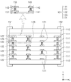
도 1은 본 발명의 일 실시 형태에 따른 코일 전자 부품을 개략적으로 나타낸 사시도이다.
도 2는 도 1의 실시 형태에서 채용될 수 있는 바디를 개략적으로 나타낸 분해사시도이다.
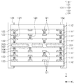
도 3은 도 1의 실시 형태에 따른 코일 전자 부품의 단면도로서, 제1 도전성 비아와 연결 패턴이 드러나도록 절단한 것이다.
도 4 내지 7은 본 발명의 변형된 실시 형태를 나타낸다.
도 8 및 도 9는 본 발명의 일 실시 형태의 코일 전자 부품에서 채용될 수 있는 연결 패턴의 형태를 개략적으로 나타낸 사시도이다.
도 10 내지 15는 본 발명의 일 실시 형태에 따른 코일 전자 부품의 제조방법을 나타내는 공정별 단면도이다.1 is a perspective view schematically showing a coil electronic component according to an embodiment of the present invention.
2 is an exploded perspective view schematically showing a body that can be employed in the embodiment of Fig.
Fig. 3 is a cross-sectional view of the coil electronic component according to the embodiment of Fig. 1, in which the first conductive via and the connection pattern are exposed.
Figures 4-7 illustrate a modified embodiment of the present invention.
Figs. 8 and 9 are perspective views schematically showing shapes of connection patterns that can be employed in a coil electronic component according to an embodiment of the present invention. Fig.
10 to 15 are cross-sectional views showing steps of a method of manufacturing a coil electronic component according to an embodiment of the present invention.
이하, 구체적인 실시형태 및 첨부된 도면을 참조하여 본 발명의 실시형태를 설명한다. 그러나, 본 발명의 실시형태는 여러 가지 다른 형태로 변형될 수 있으며, 본 발명의 범위가 이하 설명하는 실시형태로 한정되는 것은 아니다. 또한, 본 발명의 실시형태는 통상의 기술자에게 본 발명을 더욱 완전하게 설명하기 위해서 제공되는 것이다. 따라서, 도면에서의 요소들의 형상 및 크기 등은 보다 명확한 설명을 위해 과장될 수 있으며, 도면상의 동일한 부호로 표시되는 요소는 동일한 요소이다.
Hereinafter, embodiments of the present invention will be described with reference to specific embodiments and the accompanying drawings. However, the embodiments of the present invention can be modified into various other forms, and the scope of the present invention is not limited to the embodiments described below. Further, the embodiments of the present invention are provided for a more complete description of the present invention to the ordinary artisan. Accordingly, the shapes and sizes of the elements in the drawings may be exaggerated for clarity of description, and the elements denoted by the same reference numerals in the drawings are the same elements.
그리고 도면에서 본 발명을 명확하게 설명하기 위해서 설명과 관계없는 부분은 생략하고, 여러 층 및 영역을 명확하게 표현하기 위하여 두께를 확대하여 나타내었으며, 동일한 사상의 범위 내의 기능이 동일한 구성요소는 동일한 참조부호를 사용하여 설명한다. 나아가, 명세서 전체에서, 어떤 부분이 어떤 구성요소를 "포함"한다고 할 때, 이는 특별히 반대되는 기재가 없는 한 다른 구성요소를 제외하는 것이 아니라 다른 구성요소를 더 포함할 수 있는 것을 의미한다.
It is to be understood that, although the present invention has been described with reference to exemplary embodiments, it is to be understood that the invention is not limited to the disclosed embodiments, but, on the contrary, Will be described using the symbols. Further, throughout the specification, when an element is referred to as "including" an element, it means that the element may include other elements as well, without departing from the other elements unless specifically stated otherwise.
코일 전자 부품Coil electronic parts
도 1은 본 발명의 일 실시 형태에 따른 코일 전자 부품을 개략적으로 나타낸 사시도이다. 도 2는 도 1의 실시 형태에서 채용될 수 있는 바디를 개략적으로 나타낸 분해사시도이다. 도 3은 도 1의 실시 형태에 따른 코일 전자 부품의 단면도로서, 제1 도전성 비아와 연결 패턴이 드러나도록 절단한 것이다.
1 is a perspective view schematically showing a coil electronic component according to an embodiment of the present invention. 2 is an exploded perspective view schematically showing a body that can be employed in the embodiment of Fig. Fig. 3 is a cross-sectional view of the coil electronic component according to the embodiment of Fig. 1, in which the first conductive via and the connection pattern are exposed.
우선, 도 1, 도 2 및 도 3을 함께 참조하면, 코일 전자 부품(100)은 바디(110)와 그 외부에 형성된 외부 전극(131, 132)을 포함하는 구조이다. 바디(110)는 코일층(101) 및 보강층(112)을 포함하며, 여기서 보강층(112)은 코일층(101)을 이루는 절연층(111)보다 강성이 높아 바디(110)의 구조적 안정성을 향상시킬 수 있는 것으로서 도 3에 도시된 형태와 같이 코일층(101)의 상부 및 하부에 배치된다. 다만, 보강층(112)은 코일층(101)의 상부 및 하부 중 한 곳에만 배치될 수도 있다.
1, 2, and 3, the coiled
외부전극(131, 132)은 한 쌍으로 구성되며, 바디(110)의 길이 방향으로 대칭되는 위치에 배치될 수 있다. 외부전극(131, 132)은 바디(110)의 코일 패턴(111)과 접속되며 이를 사이에는 후술할 바와 같이 연결 패턴(122)이 제공될 수 있다. 외부전극(131, 132)의 구체적인 형태로서, 예컨대 최외층은 주석(Sn) 도금층이며, 그 하부에 니켈(Ni) 도금층이 형성된 구조를 사용할 수 있다.
The
이하, 도 2 및 도 3을 참조하여 바디(110)의 세부 구조를 더욱 상세히 설명한다.
Hereinafter, the detailed structure of the
코일층(101)은 복수 개 구비되어 일 방향으로 적층되며, 각각의 코일층(101)은 절연층(111), 코일 패턴(121) 및 절연층(111)을 관통하여 코일 패턴(121)과 연결된 제1 도전성 비아(123)를 포함한다. 이러한 형태에 의하여 코일층(101)의 코일 패턴(121)은 상기 적층 방향을 따라 코일 형태를 이루게 된다.
A plurality of
절연층(111)은 인덕터의 바디로 사용될 수 있는 물질 중 적절한 것을 선택할 수 있으며, 예컨대, 수지, 세라믹, 페라이트 등을 예로 들 수 있다. 본 실시 형태의 경우, 절연층(111)은 감광성 절연재를 이용할 수 있으며, 이에 의하여 포토 리소그래피 공정을 통한 미세 패턴의 구현이 가능할 수 있다. 즉, 감광성 절연재로 절연층(111)을 형성함으로써 제1 도전성 비아(123), 코일 패턴(121) 등을 미세하게 형성하여 부품(100)의 소형화 및 기능 향상에 기여할 수 있다. 이를 위하여 절연층(111)에는 예컨대 감광성 유기물이나 감광성 수지가 포함될 수 있다. 이 외에 절연층(111)에는 필러(Filler) 성분으로서 SiO2/Al2O3/BaSO4/Talc 등의 무기 성분이 더 포함될 수 있다.
The
코일 패턴(121)은 고 전도성 금속을 코일 형상으로 패터닝하여 얻어질 수 있으며, 예컨대, 동박 에칭(Cu foil etching)을 이용하는 텐팅(Tenting)법, 동도금을 이용하는 SAP(Semi Additive Process), MASP(Modified Semi Additive Process)등을 예로 들 수 있다. 코일 패턴(121)을 형성하기 위한 금속 물질의 경우, 구리(Cu), 은(Ag), 팔라듐(Pd), 알루미늄(Al), 니켈(Ni), 티타늄(Ti), 금(Au) 또는 백금(Pt) 등의 단독 또는 혼합 물질이 있다. 한편, 도 3에 도시된 형태와 같이 코일 패턴(121)은 일 표면이 노출되도록 절연층(111)에 부분 매립된 형태일 수 있으며, 이는 후술할 바와 같이 코일층(101) 각각을 따로 제작하는 과정에서 얻어질 수 있다. 여기서, 코일 패턴(121)의 일 표면이 노출된 구조는 해당 코일 패턴(121)과 동일 레벨이 존재하는 절연층(111)으로부터 노출된 형태를 의미한다. 또한, 코일층(101)을 개별적으로 마련하여 이를 적층하는 공법을 사용함으로써 바디(110)는 상하 비대칭 형태로 얻어질 수 있다. 즉, 도 3에 표현되어 있듯이, 바디(110)는 중심면을 기준으로 이에 포함된 코일층(101)과 연결 패턴(122) 등이 상하 비대칭 구조를 이룰 수 있다.
The
제1 도전성 비아(123)는 서로 다른 층에 위치한 코일 패턴(121)을 연결하기 위한 것이며, 도 3에 도시된 형태와 같이 다층 구조로 형성될 수 있다. 구체적으로, 제1 도전성 비아(123)는 Cu층(141) 및 Sn층(142)의 적층 구조를 포함하며, 이들은 예컨대, 적절한 도금 공정으로 얻어질 수 있다. 이 경우, Sn층(142)과 코일 패턴(143)의 계면에는 금속간 화합물(143)이 형성될 수 있다. 통상적인 빌드-업(Build-up) 방식의 PCB (Printed Circuit Board) 기술을 이용할 경우, 도전성 비아는 회로 패턴과 동일한 재질의 금속재료로 형성되기 때문에 금속간 화합물은 나타나지 않지만, 후술할 바와 같이 일괄 적층 공법을 사용할 경우 코일 패턴(121)을 이루는 물질과 제1 도전성 비아(123)를 이루는 물질, 예컨대, Sn이 확산 결합하여 전기적 접속이 효과적으로 이루어질 수 있다. 다만, 제1 도전성 비아(123)은 본 실시 형태와 같은 다층 구조로만 이루어지는 것은 아니며 단층 구조로 이루어질 수도 있을 것이다.
The first
상술한 바와 같이, 코일층(101)의 외곽에 배치되어 바디(110)의 커버를 이루는 보강층(112)은 절연층(111)보다 강성이 높다. 미세 패턴을 구현하기 위하여 감광성 물질을 사용하는 경우 절연층(111)의 강성은 저하될 수 있으며, 보강층(112)은 이러한 강성의 저하를 방지한다. 보강층(112)은 세라믹 등으로 이루어진 필러를 포함하며, 절연층(111)에 비하여 이러한 필러가 많이 충진됨으로써 높은 강성을 얻을 수 있다. 절연층(111)보다 강성이 높은 경우 보강층(112)의 이러한 기능이 구현될 수 있다 할 것이며, 구체적인 특성의 실제 예를 들자면, 보강층(112)의 영률(Young's modulus)은 약 12 이상일 수 있다. 또한, 본 실시 형태에서는 보강층(112)이 바디(110)의 상부와 하부에 각각 하나씩 적층된 형태를 설명하고 있지만, 필요에 따라 보강층(112)의 개수는 늘어날 수 있으며, 예컨대, 복수의 보강층(112)을 같은 위치에 적층할 수도 있을 것이다.
As described above, the reinforcing
한편, 본 실시 형태의 경우, 코일층(101)은 절연층(111)의 코너에 형성되어 외부 전극(131, 132)과 연결된 연결 패턴(122)을 포함할 수 있다. 연결 패턴(122)에 의하여 코일 패턴(121)과 외부 전극(131, 132)이 안정적으로 결합되며, 전기적 특성이 향상될 수 있다. 코일 패턴(121)과 마찬가지로 연결 패턴(122)은 Cu 등의 물질을 이용하여 형성될 수 있으며, 도 2에 도시된 형태와 같이 상부에서 보았을 때 'L'자 형상을 가질 수 있다. 이러한 'L'자 형상의 연결 패턴(122)에 의하여 외부 전극(131, 132)과의 결합력이 향상될 수 있다.
The
또한, 서로 다른 층에 배치된 연결 패턴(122)을 서로 연결하기 위하여 코일층(101)은 절연층(111)을 관통하여 연결 패턴(122)과 연결된 제2 도전성 비아(124)를 포함할 수 있다. 이 경우, 제2 도전성 비아(124)는 제1 도전성 비아(123)와 유사하거나 동일한 구조를 가질 수 있다. 구체적으로, 제2 도전성 비아(124)는 Cu층(151) 및 Sn층(152)의 적층 구조일 수 있으며, 이와 연결된 연결 패턴(122)과의 계면에는 금속간 화합물(153)이 형성될 수 있다.
The
연결 패턴(122)과 코일 패턴(121)의 연결 구조의 경우, 도 2에 도시된 형태와 같이, 복수의 코일층(101) 중 최상부 및 최하부에 배치된 것은 코일 패턴(121)과 연결 패턴(122)이 연결된 형태이다. 이와 반대로, 복수의 코일층(101) 중 최상부 및 최하부에 배치된 것을 제외한 나머지(중간에 배치된 4개의 코일층)는 코일 패턴(121)과 연결 패턴(122)이 연결되어 있지 아니한 형태이다.
In the case of the connection structure of the
한편, 본 실시 형태에서는 각 코일층(101)에 한 쌍의 연결 패턴(122)이 형성되어 한 쌍의 외부 전극(131, 132)과 접속된 형태를 나타내고 있지만, 연결 패턴(122)의 개수는 변화할 수 있다. 예컨대, 절연층(111)의 네 모서리 모두에 연결 패턴(122)이 형성될 수도 있다. 나아가, 연결 패턴(122)의 배치된 위치 역시 도 2에 도시된 형태에서 변화될 수 있으며, 예컨대, 절연층(111)에서 대각선 방향으로 서로 마주하는 2개의 코너에 한 쌍의 연결 패턴(122)이 형성될 수도 있다.
In the present embodiment, a pair of
또한, 본 실시 형태에서는 제2 도전성 비아(124)는 적층 방향으로 일정한 위치에 배치되어 있으나 필요에 따라 제2 도전성 비아(124)의 위치는 변경될 수 있으며, 도 8 및 도 9를 참조하여 이를 설명한다. 도 8 및 도 9는 본 발명의 일 실시 형태의 코일 전자 부품에서 채용될 수 있는 연결 패턴의 형태를 개략적으로 나타낸 사시도이다. 변형된 형태의 경우, 제2 도전성 비아(124`, 124``)는 인접한 다른 코일층에 포함된 것과 적층 방향으로 오버랩 되지 않는 위치에 배치되며, 이러한 예로서, 도 8 및 도 9에 도시된 형태와 같이 제2 도전성 비아(124`, 124``)는 적층 방향을 기준으로 지그재그 형태로 배열될 수 있다.
In this embodiment, the second conductive via 124 is disposed at a predetermined position in the stacking direction, but the position of the second conductive via 124 may be changed if necessary. Referring to FIGS. 8 and 9, Explain. Figs. 8 and 9 are perspective views schematically showing shapes of connection patterns that can be employed in a coil electronic component according to an embodiment of the present invention. Fig. In the modified form, the second conductive vias 124 'and 124''are disposed at positions that do not overlap in the stacking direction with those included in the adjacent other coil layers, and as an example, as shown in FIGS. 8 and 9 The second
이러한 지그재그 형태의 배열의 경우, 제2 도전성 비아(124`, 124``)의 작용하는 압력이 분산될 수 있으며, 이에 따라 바디(110)에서 내에서 발생할 수 있는 두께 편차 등의 공정 변수에 따른 영향을 저감할 수 있다. 즉, 적층형 인덕터의 경우 각 코일층(101) 간의 거리와 코일 패턴(121)의 두께 등에 따라 특성에 큰 변화를 보이는데, 절연층(111)과 코일 패턴(121) 등의 도체층은 경도 및 모듈러스 등의 특성이 다르다. 따라서, 열과 압력으로 압착 시 바디(110) 내에서는 두께 편차가 발생 할 수 있으며, 제2 도전성 비아(124`, 124``)를 지그재그 배치함으로써 이를 개선할 수 있는 것이다.
In this zigzag arrangement, the working pressure of the second
한편, 제2 도전성 비아(124`, 124``)의 형상은 도 8에 도시된 것과 같이 원 기둥일 수 있으며, 이와 달리, 도 8에 도시된 것과 같이 사각 기둥으로 형성하여 접촉 면적을 더욱 증가시킬 수도 있을 것이다.
The shape of the second conductive vias 124 'and 124' may be a circular column as shown in FIG. 8, or alternatively, may be formed as a square column as shown in FIG. 8 to further increase the contact area It can be done.
이하, 도 4 내지 7을 참조하여 본 발명의 변형된 실시 형태를 설명하되, 앞선 실시 형태에서 변경된 요소만을 다루기로 한다. 우선, 도 4의 실시 형태의 경우, 제2 도전성 비아(224)의 형태 면에서 앞선 실시 형태와 차이가 있다. 구체적으로 연결 패턴(122)의 층간 연결을 위하여 제2 도전성 비아(224)는 복수의 코일층(101) 전체를 관통하는 일체 구조로 제공될 수 있다. 이를 위하여 아래에서 설명할 공정과 달리 개별 코일층(101)의 제작 시 연결 패턴(122)과 접속된 비아를 따로 형성하지 않고, 코일층(101)을 적층한 후 이를 관통하는 스루홀을 형성할 수 있다. 이러한 스루홀을 충진하도록 Cu 등의 물질로 도금함으로써 복수의 코일층(101)을 관통하여 연결 패턴(122)과 접속된 제2 도전성 비아(224)를 구현할 수 있다.
Hereinafter, modified embodiments of the present invention will be described with reference to Figs. 4 to 7, but only the elements that have changed in the foregoing embodiments will be described. First, the embodiment of FIG. 4 differs from the preceding embodiment in terms of the shape of the second conductive via 224. Specifically, the second
다음으로 도 5의 실시 형태의 경우, 앞선 실시 형태에서 패드층(113)이 더 포함되며, 이는 코일층(101)과 보강층(112) 사이에 배치된다. 패드층(113)은 외부 전극(131, 132)과 연결된 연결 패턴(122)을 구비하는 점에서는 코일층(101)과 유사하지만, 코일 패턴(121)은 따로 구비하지 않는다. 이러한 패드층(113)은 코일 전자 부품(100)의 크기를 유지한 상태에서 코일층(101)의 크기나 코일 패턴(112)의 턴수 등을 조절하기 위하여 채용될 수 있다.
Next, in the case of the embodiment of FIG. 5, a
다음으로, 도 6의 실시 형태는 중심에 코어부(201)를 더 포함하는 형태로서 구조적인 안정성을 더욱 향상시킬 수 있다. 구체적으로, 바디(110)의 중심부에는 코어부(201)가 배치되며, 코일층(101`)은 코어부(201)의 상부 및 하부에 배치된 형태이다. 코어부(201)는 기재(202)와 그 표면에 형성된 도전성 패턴(203) 및 관통 배선(204)를 구비하여 코일 패턴(121) 및 연결 패턴(122)과 접속될 수 있다. 이러한 형태를 갖는 것으로서 동박 적층판(CCL)을 사용하고 이를 적절히 가공하여 코어부(201)를 형성할 수 있다.
Next, the embodiment of Fig. 6 can further improve the structural stability as a form including the
코어부(201)를 사용하는 본 변형 예의 경우, 코일층(101`) 중 코어부(201)의 상부에 배치된 것(도 6을 기준으로 코어부 위의 3개의 코일층)과 하부에 배치된 것(코어부 아래의 3개의 코일층) 모두 이에 포함된 제1 도전성 비아(123)가 코어부(201)를 향하도록 배치될 수 있다. 이러한 배치 형태는 복수의 코일층(101`)을 제작한 후 이들을 코어부(201)를 중심으로 적층하는 경우, 보다 안정적인 접속 구조를 얻기 위하여 채용될 수 있다.
In the case of this modification using the
다음으로, 도 7의 실시 형태의 경우, 도 1의 실시 형태와 외부 전극이 형성된 위치 면에서 차이가 있으며, 바디(110)는 동일한 것을 채용할 수 있다. 구체적으로 본 변형 예에서는 외부 전극(131`, 132`)이 연결 패턴(122)에 대응하는 영역, 즉, 바디(110)의 코너 영역에 형성될 수 있다. 바디(110)에서 외부 전극(131`, 132`)이 차지하는 영역이 최소화됨에 따라 불필요하게 발생할 수 있는 특성 저하, 예컨대, 코일 패턴과 외부 전극(131`, 132`)에 의하여 발생하는 기생 커패시턴스 등을 저감할 수 있다.
Next, in the case of the embodiment of Fig. 7, there is a difference between the embodiment of Fig. 1 and the position in which the external electrode is formed, and the
코일 전자 부품의 제조방법Manufacturing method of coil electronic parts
이하, 도 10 내지 15를 참조하여 상술한 구조를 갖는 코일 전자 부품의 제조방법의 일 예를 설명한다.
Hereinafter, an example of a method of manufacturing a coil electronic component having the above-described structure with reference to Figs. 10 to 15 will be described.
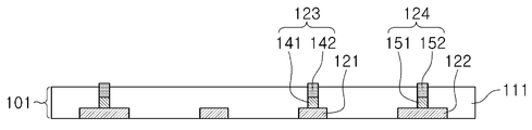
상술한 바와 같이 상술한 코일 전자 부품은 코일층과 보강층을 일괄 적층하는 방법으로 제조될 수 있으며, 그 예로서, 도 10 내지 14에 도시된 형태와 같이 절연층(111), 코일 패턴(121), 제1 도전성 비아(123) 등을 포함하는 개별 코일층(101)을 제작한다. 구체적으로, 우선 도 10 및 도 11에 도시된 형태와 같이, 캐리어층(301)을 마련하여 그 표면에 코일 패턴(121)을 형성한다. 이 경우, 코일 패턴(121)의 형성 과정에서 연결 패턴(122)도 함께 형성될 수 있다. 캐리어층(301)은 열 경화성 수지의 재질로 이루어질 수 있으며, 표면에는 동박층(302, 303)이 형성되어 있을 수 있다. 이에 따라, 캐리어층(301)은 동박 적층판(Copper Clad Laminate)의 형태로 제공될 수 있다. 동박층(302, 303)은 코일 패턴(121)의 형성을 위한 시드나 후속 공정에서 캐리어층(301)을 용이하기 분리하는 기능 등을 수행하며, 실시 형태에 따라서는 제외될 수도 있을 것이다.
As described above, the coil electronic component may be manufactured by a method of collectively laminating a coil layer and a reinforcing layer. For example, as shown in FIGS. 10 to 14, an insulating
코일 패턴(121)과 연결 패턴(122)은 동박층(303) 상에 마스크층을 적층 및 패터닝한 후 Cu 등을 도금하여 얻어질 수 있으며, 이후 상기 마스크층은 제거된다. 그리고, 코일 패턴(121)과 연결 패턴(122)은 캐리어층(301)의 상면 및 하면에 모두 형성되며, 이에 의하여 단일 공정으로 2개의 코일층(101)을 얻을 수 있다.
The
다음으로, 도 12에 도시된 형태와 같이, 코일 패턴(121) 및 연결 패턴(122)을 덮도록 절연층(111)을 형성하며, 절연층(111)은 캐리어층(301) 상면 및 하면 모두에 적용될 수 있다. 상술한 바와 같이, 절연층(111)은 감광성 절연재를 사용하며, 예컨대 진공 라미네이터를 이용하여 도포될 수 있다. 이 경우, 절연층(111)은 약 10-80um의 두께를 가질 수 있으며, 필요한 목적에 따라 금속이나 세라믹 필러를 함유할 수 있다. 또한, 절연층(111)에 포함되는 감광성 물질의 양에 의하여 절연층(111)의 경화도가 조절될 수 있으며, 열 경화성 물질과 감광성 물질을 2종 이상 혼합할 수도 있다.
12, an insulating
다음으로, 도 13에 도시된 형태와 같이, 코일 패턴(121)과 연결되도록 제1 도전성 비아(123)를 형성한다. 이를 위하여, 감광성 절연재인 절연층(111)을 UV 등으로 노광 및 현상하여 관통 홀을 형성한 후 이를 채우도록 Cu층(141)과 Sn층(142)을 도금 형성할 수 있다. 또한, 이와 같은 방식으로 Cu층(151)과 Sn층(152)을 포함하는 제2 도전성 비아(124)를 형성할 수 있다.
Next, as shown in FIG. 13, a first conductive via 123 is formed to be connected to the
다음으로, 도 14에 도시된 것과 같이 코일층(101)으로부터 캐리어층(301)을 분리하여 개별 코일층(101)을 얻으며, 도 13에서는 하나의 코일층(101)만을 도시하였다. 상술한 바와 같이 동박층(302)에 의하여 캐리어층(301)은 용이하게 분리될 수 있다. 또한, 코일층(101) 하부에 잔존하는 동박층(303)의 경우 당 기술 분야에서 알려진 에칭 공정을 적절히 적용하여 제거될 수 있다.
Next, as shown in Fig. 14, the
상술한 공정을 통하여 개별 코일층(101)을 필요한 개수만큼 제조하며, 이 경우, 각 코일층(101)에 포함된 코일 패턴(121)과 연결 패턴(122) 등의 형상은 서로 달라질 수 있을 것이다. 코일층(101)의 제작과 별도로 절연층(111)보다 강성이 높은 보강층(112)을 제작하며, 보강층(112)은 절연성 수지에 상대적으로 다량의 세라믹 필러를 포함할 수 있다. 이렇게 얻어진 코일층(101)과 보강층(112)을 도 15에 도시된 형태와 같이, 일괄적으로 적층하며, 이 경우 열과 압력을 가하여 적층 구조물을 얻을 수 있다. 이 경우, 강성 강화를 위하여 보강층(112)은 최상부와 최하부에 배치된다.
The required number of the individual coil layers 101 may be manufactured through the above-described processes. In this case, the shapes of the
이렇게 얻어진 바디는 따로 소성 공정을 거치지 않고도 안정적으로 층간 결합이 구현될 수 있다. 마지막으로 바디의 외부에 외부전극(131, 132)을 형성하여 상술한 코일 전자 부품(100)을 구현할 수 있으며, 외부전극(131, 132)은 도전성 페이스트를 도포하거나, 도금 공정 등을 이용하여 형성할 수 있을 것이다.
The resulting body can be stably interlaminar bonded without a separate firing step. Finally, the
본 실시 형태와 같이, 미리 제작된 코일층(101)과 보강층(112)을 한번에 적층하여 바디를 형성함으로써 각 층을 순차적으로 적층하는 공법과 비교하여 전체 공정 수와 공정 시간을 줄일 수 있으며, 이는 공정 비용 감소로 이어진다. 또한, 본 실시 형태에 따른 제조 방법의 경우, 코일층(101)의 개수나 두께를 적절히 조절함으로써 코일 전자 부품(100)의 크기, 전기적 특성 등의 사양을 효과적으로 구현하는 데에도 유리하다. 다만, 본 실시 형태에서는 코일층(101)과 보강층(112) 모두를 한번에 적층하였으나 코일층(101)과 보강층(112)의 개수에 따라 2회나 그 이상으로 나누어서 적층할 수도 있을 것이다.
The total number of processes and the process time can be reduced as compared with the method of stacking the layers in advance by laminating the
본 발명은 상술한 실시 형태 및 첨부된 도면에 의해 한정되는 것이 아니며, 첨부된 청구범위에 한정하고자 한다. 따라서, 청구범위에 기재된 본 발명의 기술적 사상을 벗어나지 않는 범위 내에서 당 기술분야의 통상의 지식을 가진 자에 의해 다양한 형태의 치환, 변형 및 변경이 가능할 것이며, 이 또한 본 발명의 범위에 속한다고 할 것이다.
The present invention is not limited to the above-described embodiments and the accompanying drawings, but is intended to be limited only by the appended claims. It will be apparent to those skilled in the art that various changes in form and details may be made therein without departing from the spirit and scope of the invention as defined by the appended claims. something to do.
100: 코일 전자 부품
101, 101`: 코일층
110: 바디
111, 111`: 절연층
112: 보강층
113: 패드층
121: 코일 패턴
122: 연결 패턴
123: 제1 도전성 비아
124, 124`, 124``: 제2 도전성 비아
131, 131`, 132, 132`: 외부 전극
141, 151: Cu층
142, 152: Sn층
143, 153: 금속간 화합물
201: 코어부
202: 기재
203: 도전성 패턴
204: 관통 배선
301: 캐리어층
302, 303: 동박층100: coil electronic parts
101, 101 ': coil layer
110: Body
111, 111`: insulating layer
112: reinforced layer
113: pad layer
121: Coil pattern
122: Connection pattern
123: First conductive vias
124, 124`, 124``: The second conductive vias
131, 131`, 132, 132`: external electrodes
141, 151: Cu layer
142, 152: Sn layer
143, 153: intermetallic compound
201: core portion
202: substrate
203: conductive pattern
204: Through-
301: Carrier layer
302, 303: copper foil layer
Claims (23)
상기 바디 외부에 형성된 외부 전극;을 포함하며,
상기 코일층은 절연층, 코일 패턴 및 상기 절연층을 관통하여 상기 코일 패턴과 연결된 제1 도전성 비아를 포함하며,
상기 보강층은 상기 절연층보다 강성이 높은 코일 전자 부품.
A body including a coil layer and a reinforcing layer disposed on at least one of an upper portion and a lower portion of the coil layer; And
And an outer electrode formed outside the body,
Wherein the coil layer includes an insulating layer, a coil pattern, and a first conductive via penetrating the insulating layer and connected to the coil pattern,
Wherein the reinforcing layer is higher in rigidity than the insulating layer.
상기 절연층은 감광성 절연재인 것을 특징으로 하는 코일 전자 부품.
The method according to claim 1,
Wherein the insulating layer is a photosensitive insulating material.
상기 코일층은 상기 절연층의 코너에 형성되어 상기 외부 전극과 연결된 연결 패턴을 더 포함하는 코일 전자 부품.
The method according to claim 1,
Wherein the coil layer further comprises a connection pattern formed at a corner of the insulating layer and connected to the external electrode.
상기 코일층은 복수 개 구비되어 일 방향으로 적층되며, 상기 복수의 코일층은 상기 절연층을 관통하여 상기 연결 패턴과 연결된 제2 도전성 비아를 더 포함하는 코일 전자 부품.
The method of claim 3,
Wherein the plurality of coil layers are stacked in one direction, and the plurality of coil layers further include a second conductive via connected to the connection pattern through the insulating layer.
상기 복수의 코일층 중 최상부 및 최하부에 배치된 것은 상기 코일 패턴과 상기 연결 패턴이 연결된 형태인 것을 특징으로 하는 코일 전자 부품.
5. The method of claim 4,
Wherein the coil pattern and the connection pattern are connected to each other at the top and bottom of the plurality of coil layers.
상기 복수의 코일층 중 최상부 및 최하부에 배치된 것을 제외한 나머지는 상기 코일 패턴과 상기 연결 패턴이 연결되어 있지 아니한 형태인 것을 특징으로 하는 코일 전자 부품.
6. The method of claim 5,
Wherein the coil pattern and the connection pattern are not connected to each other except for the uppermost and lowermost portions of the plurality of coil layers.
상기 제2 도전성 비아는 Cu층 및 Sn층의 적층 구조인 것을 특징으로 하는 코일 전자 부품.
5. The method of claim 4,
Wherein the second conductive via is a laminated structure of a Cu layer and a Sn layer.
상기 제2 도전성 비아는 인접한 다른 코일층에 포함된 것과 상기 적층 방향으로 오버랩 되지 않는 위치에 배치된 것을 특징으로 하는 코일 전자 부품.
5. The method of claim 4,
Wherein the second conductive via is disposed at a position not overlapping with that included in another adjacent coil layer and in the stacking direction.
상기 제2 도전성 비아는 상기 복수의 코일층 전체를 관통하는 일체 구조인 것을 특징으로 하는 코일 전자 부품.
5. The method of claim 4,
And the second conductive vias are integrated with each other through the entirety of the plurality of coil layers.
상기 연결 패턴은 상부에서 보았을 때 'L'자 형상을 갖는 것을 특징으로 하는 코일 전자 부품.
The method of claim 3,
Wherein the connection pattern has an L shape when viewed from above.
상기 코일층과 상기 보강층 사이에 배치되며, 상기 외부 전극과 연결된 연결 패턴을 구비하되 코일 패턴은 구비하지 않는 패드층을 더 포함하는 코일 전자 부품.
The method of claim 3,
And a pad layer disposed between the coil layer and the reinforcing layer and having a connection pattern connected to the external electrode, but not including a coil pattern.
상기 코일 패턴은 일 표면이 노출되도록 상기 절연층에 부분 매립된 형태인 것을 특징으로 하는 코일 전자 부품.
The method according to claim 1,
Wherein the coil pattern is partially buried in the insulating layer so that one surface thereof is exposed.
상기 보강층의 영률은 12 이상인 것을 특징으로 하는 코일 전자 부품.
The method according to claim 1,
And the Young's modulus of the reinforcing layer is 12 or more.
상기 제1 도전성 비아는 Cu층 및 Sn층의 적층 구조인 것을 특징으로 하는 코일 전자 부품.
The method according to claim 1,
Wherein the first conductive via is a laminated structure of a Cu layer and a Sn layer.
상기 제1 도전성 비아는 상기 Sn층과 상기 코일 패턴의 계면에 형성된 금속간 화합물을 더 포함하는 코일 전자 부품.
15. The method of claim 14,
Wherein the first conductive via further comprises an intermetallic compound formed at an interface between the Sn layer and the coil pattern.
상기 바디는 중심면을 기준으로 상하 비대칭 구조인 것을 특징으로 하는 코일 전자 부품.
The method according to claim 1,
Wherein the body is vertically asymmetric with respect to a center plane.
상기 바디는 중심부에 배치된 코어부를 더 포함하며, 상기 코일층은 상기 코어부 상하부에 배치된 것을 특징으로 하는 코일 전자 부품.
The method according to claim 1,
Wherein the body further comprises a core portion disposed at a central portion, and the coil layer is disposed at the upper and lower portions of the core portion.
상기 코일층 중 상기 코어부의 상부에 배치된 것과 하부에 배치된 것 모두 이에 포함된 제1 도전성 비아가 상기 코어부를 향하도록 배치된 것을 특징으로 하는 코일 전자 부품.
18. The method of claim 17,
Wherein the first conductive vias disposed in the upper portion of the coil portion and the lower portion of the coil layer are disposed to face the core portion.
상기 코어부는 동박 적층판인 것을 특징으로 하는 코일 전자 부품.
18. The method of claim 17,
Wherein the core portion is a copper-clad laminate.
상기 절연층보다 강성이 높은 보강층을 마련하는 단계;
상기 복수 개의 코일층과 상기 복수 개의 코일층의 상부 및 하부 중 적어도 한 곳에 상기 보강층을 일괄 적층하여 바디는 형성하는 단계; 및
상기 바디의 외부에 외부 전극을 형성하는 단계;
를 포함하는 코일 전자 부품의 제조방법.
Providing a plurality of coil layers including an insulating layer, a coil pattern, and a first conductive via penetrating the insulating layer and connected to the coil pattern;
Providing a reinforcing layer having higher rigidity than the insulating layer;
Stacking the reinforcing layers in at least one of the plurality of coil layers and the upper and lower portions of the plurality of coil layers to form a body; And
Forming an external electrode on the outside of the body;
Wherein the coil electronic component is a coil.
상기 코일층을 마련하는 단계는,
캐리어층의 표면에 상기 코일 패턴을 형성하는 단계와, 상기 코일 패턴을 덮도록 상기 절연층을 형성하는 단계 및 상기 절연층을 관통하여 상기 코일 패턴과 연결된 상기 제1 도전성 비아를 형성하는 단계를 포함하는 코일 전자 부품의 제조방법.
21. The method of claim 20,
The step of providing the coil layer may include:
Forming the coil pattern on the surface of the carrier layer; forming the insulating layer to cover the coil pattern; and forming the first conductive via through the insulating layer and connected to the coil pattern Of the coil.
상기 코일층을 마련하는 단계는 상기 코일층으로부터 상기 캐리어층을 분리하는 단계를 더 포함하는 코일 전자 부품의 제조방법.
22. The method of claim 21,
Wherein the step of providing the coil layer further comprises separating the carrier layer from the coil layer.
상기 코일층은 상기 캐리어층의 상면 및 하면에 모두 형성되는 것을 특징으로 하는 코일 전자 부품의 제조방법.22. The method of claim 21,
Wherein the coil layer is formed on both the upper surface and the lower surface of the carrier layer.
Priority Applications (3)
| Application Number | Priority Date | Filing Date | Title |
|---|---|---|---|
| KR1020160046375A KR101883046B1 (en) | 2016-04-15 | 2016-04-15 | Coil Electronic Component |
| JP2016098855A JP6880525B2 (en) | 2016-04-15 | 2016-05-17 | Manufacturing method of coil electronic parts and coil electronic parts |
| US15/232,325 US10650958B2 (en) | 2016-04-15 | 2016-08-09 | Coil electronic component |
Applications Claiming Priority (1)
| Application Number | Priority Date | Filing Date | Title |
|---|---|---|---|
| KR1020160046375A KR101883046B1 (en) | 2016-04-15 | 2016-04-15 | Coil Electronic Component |
Publications (2)
| Publication Number | Publication Date |
|---|---|
| KR20170118503A true KR20170118503A (en) | 2017-10-25 |
| KR101883046B1 KR101883046B1 (en) | 2018-08-24 |
Family
ID=60040130
Family Applications (1)
| Application Number | Title | Priority Date | Filing Date |
|---|---|---|---|
| KR1020160046375A KR101883046B1 (en) | 2016-04-15 | 2016-04-15 | Coil Electronic Component |
Country Status (3)
| Country | Link |
|---|---|
| US (1) | US10650958B2 (en) |
| JP (1) | JP6880525B2 (en) |
| KR (1) | KR101883046B1 (en) |
Cited By (2)
| Publication number | Priority date | Publication date | Assignee | Title |
|---|---|---|---|---|
| KR20190096212A (en) * | 2018-02-08 | 2019-08-19 | 삼성전기주식회사 | Inductor |
| KR20200070833A (en) * | 2018-12-10 | 2020-06-18 | 삼성전기주식회사 | Coil electronic component |
Families Citing this family (5)
| Publication number | Priority date | Publication date | Assignee | Title |
|---|---|---|---|---|
| JP6658415B2 (en) | 2016-09-08 | 2020-03-04 | 株式会社村田製作所 | Electronic components |
| KR101942732B1 (en) * | 2017-04-12 | 2019-01-28 | 삼성전기 주식회사 | Inductor and manufacturing method of the same |
| JP6838548B2 (en) * | 2017-12-07 | 2021-03-03 | 株式会社村田製作所 | Coil parts and their manufacturing methods |
| KR102004813B1 (en) | 2018-02-09 | 2019-07-29 | 삼성전기주식회사 | Coil component and manufacturing method for the same |
| JP7247818B2 (en) | 2019-08-29 | 2023-03-29 | 株式会社村田製作所 | multilayer inductor |
Family Cites Families (31)
| Publication number | Priority date | Publication date | Assignee | Title |
|---|---|---|---|---|
| JPS6041312A (en) * | 1983-08-16 | 1985-03-05 | Tdk Corp | Circuit element |
| JP3123209B2 (en) | 1992-05-01 | 2001-01-09 | 株式会社村田製作所 | Composite electronic components |
| JP2001345212A (en) * | 2000-05-31 | 2001-12-14 | Tdk Corp | Laminated electronic part |
| JP4055978B2 (en) | 2000-10-02 | 2008-03-05 | Tdk株式会社 | Manufacturing method of high frequency coil |
| JP2002359141A (en) * | 2001-05-31 | 2002-12-13 | Ngk Spark Plug Co Ltd | Manufacturing method of laminated electronic component |
| JP2002368524A (en) | 2001-06-11 | 2002-12-20 | Ajinomoto Co Inc | Coil production method and new coil |
| JP4374880B2 (en) * | 2003-03-27 | 2009-12-02 | 株式会社村田製作所 | Multilayer coil and manufacturing method thereof |
| JP2005277385A (en) * | 2004-02-27 | 2005-10-06 | Tdk Corp | Laminate chip inductor forming member and method of manufacturing laminate chip inductor comonent |
| JP2007134555A (en) * | 2005-11-11 | 2007-05-31 | Matsushita Electric Ind Co Ltd | Electronic component and its manufacturing method |
| CN101361146B (en) * | 2006-01-16 | 2011-09-07 | 株式会社村田制作所 | Method for manufacturing inductor |
| US7852186B2 (en) * | 2006-08-28 | 2010-12-14 | Avago Technologies Ecbu Ip (Singapore) Pte. Ltd. | Coil transducer with reduced arcing and improved high voltage breakdown performance characteristics |
| KR101174541B1 (en) * | 2007-02-02 | 2012-08-16 | 가부시키가이샤 무라타 세이사쿠쇼 | laminated coil component |
| JP2009130325A (en) * | 2007-11-28 | 2009-06-11 | Murata Mfg Co Ltd | Laminated electronic component |
| JP2009152347A (en) * | 2007-12-20 | 2009-07-09 | Panasonic Corp | Coil component, and manufacturing method thereof |
| CN102007551B (en) | 2008-04-28 | 2013-06-26 | 株式会社村田制作所 | Multilayer coil component and method for manufacturing the same |
| JP2009277972A (en) * | 2008-05-16 | 2009-11-26 | Panasonic Corp | Coil component and method of manufacturing the same |
| JP2010165975A (en) * | 2009-01-19 | 2010-07-29 | Murata Mfg Co Ltd | Laminated inductor |
| JP5543883B2 (en) * | 2010-09-24 | 2014-07-09 | 太陽誘電株式会社 | Common mode noise filter |
| KR101218985B1 (en) * | 2011-05-31 | 2013-01-04 | 삼성전기주식회사 | Chip-type coil component |
| CN103608875B (en) * | 2011-06-15 | 2016-06-29 | 株式会社村田制作所 | Electronic unit and manufacture method thereof |
| JP5765633B2 (en) * | 2011-12-22 | 2015-08-19 | 株式会社フジクラ | Printed wiring board and manufacturing method thereof |
| JP5962754B2 (en) | 2012-03-27 | 2016-08-03 | 株式会社村田製作所 | Electronic components |
| JP5761248B2 (en) * | 2013-04-11 | 2015-08-12 | 株式会社村田製作所 | Electronic components |
| JP5888289B2 (en) * | 2013-07-03 | 2016-03-16 | 株式会社村田製作所 | Electronic components |
| JP6064854B2 (en) * | 2013-09-30 | 2017-01-25 | 株式会社村田製作所 | Electronic component and manufacturing method thereof |
| JP6064860B2 (en) * | 2013-10-09 | 2017-01-25 | 株式会社村田製作所 | Composite electronic component and method of manufacturing composite electronic component |
| JP6425375B2 (en) * | 2013-10-11 | 2018-11-21 | 新光電気工業株式会社 | Coil substrate and method of manufacturing the same, inductor |
| JP6381432B2 (en) * | 2014-05-22 | 2018-08-29 | 新光電気工業株式会社 | Inductor, coil substrate, and method of manufacturing coil substrate |
| JP6564614B2 (en) * | 2014-05-22 | 2019-08-21 | 新光電気工業株式会社 | Inductor and method of manufacturing inductor |
| US10147533B2 (en) * | 2015-05-27 | 2018-12-04 | Samsung Electro-Mechanics Co., Ltd. | Inductor |
| JP6740668B2 (en) * | 2016-03-30 | 2020-08-19 | Tdk株式会社 | Thin film inductor |
-
2016
- 2016-04-15 KR KR1020160046375A patent/KR101883046B1/en active IP Right Grant
- 2016-05-17 JP JP2016098855A patent/JP6880525B2/en active Active
- 2016-08-09 US US15/232,325 patent/US10650958B2/en active Active
Cited By (2)
| Publication number | Priority date | Publication date | Assignee | Title |
|---|---|---|---|---|
| KR20190096212A (en) * | 2018-02-08 | 2019-08-19 | 삼성전기주식회사 | Inductor |
| KR20200070833A (en) * | 2018-12-10 | 2020-06-18 | 삼성전기주식회사 | Coil electronic component |
Also Published As
| Publication number | Publication date |
|---|---|
| US10650958B2 (en) | 2020-05-12 |
| KR101883046B1 (en) | 2018-08-24 |
| JP6880525B2 (en) | 2021-06-02 |
| JP2017191923A (en) | 2017-10-19 |
| US20170301453A1 (en) | 2017-10-19 |
Similar Documents
| Publication | Publication Date | Title |
|---|---|---|
| KR101883046B1 (en) | Coil Electronic Component | |
| JP6665838B2 (en) | Inductor components | |
| KR102260374B1 (en) | Inductor and method of maufacturing the same | |
| US10847300B2 (en) | Inductor and method of manufacturing the same | |
| KR102463330B1 (en) | Coil Electronic Component | |
| EP3104408B1 (en) | Package structure and method for manufacturing the same | |
| JP6614246B2 (en) | Capacitor built-in multilayer wiring board and manufacturing method thereof | |
| US20120055706A1 (en) | Printed circuit board and method of manufacturing the same | |
| JP7294584B2 (en) | Inductor and its manufacturing method | |
| KR102545033B1 (en) | Coil Electronic Component | |
| US10515755B2 (en) | Coil electronic component and method of manufacturing the same | |
| JP2008159973A (en) | Electronic component module and circuit board with built-in components incorporating the module | |
| KR102281452B1 (en) | A printed circuit board comprising embeded electronic component within and a method for manufacturing | |
| US11017936B2 (en) | Coil electronic component | |
| US10123418B1 (en) | Circuit board structure and manufacturing method thereof | |
| CN110087392B (en) | Circuit board structure and manufacturing method thereof | |
| KR101872525B1 (en) | Printed circuit board and method for manufacturing the same | |
| KR102574413B1 (en) | Coil electronic component | |
| KR102281458B1 (en) | Printed circuit board having an embedded device, semiconductor package and method of manufacturing the same | |
| KR101553474B1 (en) | Method of manufacturing embedded type printed circuit board and stack package including the embedded type printed circuit board | |
| JP7355051B2 (en) | Inductor components and electronic components | |
| JP4802575B2 (en) | Electric circuit board | |
| KR102172678B1 (en) | Printed circuit board and method for manufacturing the same | |
| JP2013219291A (en) | Electronic module | |
| CN115036110A (en) | Inductance component |
Legal Events
| Date | Code | Title | Description |
|---|---|---|---|
| A201 | Request for examination | ||
| E902 | Notification of reason for refusal | ||
| E701 | Decision to grant or registration of patent right | ||
| GRNT | Written decision to grant |