JP6425375B2 - Coil substrate and method of manufacturing the same, inductor - Google Patents
Coil substrate and method of manufacturing the same, inductor Download PDFInfo
- Publication number
- JP6425375B2 JP6425375B2 JP2013214129A JP2013214129A JP6425375B2 JP 6425375 B2 JP6425375 B2 JP 6425375B2 JP 2013214129 A JP2013214129 A JP 2013214129A JP 2013214129 A JP2013214129 A JP 2013214129A JP 6425375 B2 JP6425375 B2 JP 6425375B2
- Authority
- JP
- Japan
- Prior art keywords
- wiring
- insulating layer
- coil
- laminate
- exposed
- Prior art date
- Legal status (The legal status is an assumption and is not a legal conclusion. Google has not performed a legal analysis and makes no representation as to the accuracy of the status listed.)
- Active
Links
- 239000000758 substrate Substances 0.000 title claims description 159
- 238000004519 manufacturing process Methods 0.000 title claims description 36
- 239000002184 metal Substances 0.000 claims description 119
- 229910052751 metal Inorganic materials 0.000 claims description 119
- 229920005989 resin Polymers 0.000 claims description 44
- 239000011347 resin Substances 0.000 claims description 44
- 238000000034 method Methods 0.000 claims description 34
- 238000009413 insulation Methods 0.000 claims description 5
- 238000010030 laminating Methods 0.000 claims description 5
- 239000000696 magnetic material Substances 0.000 claims description 5
- 238000003825 pressing Methods 0.000 claims description 3
- 239000010410 layer Substances 0.000 description 301
- 239000012790 adhesive layer Substances 0.000 description 81
- 239000010949 copper Substances 0.000 description 30
- 238000007789 sealing Methods 0.000 description 23
- 239000000463 material Substances 0.000 description 18
- RYGMFSIKBFXOCR-UHFFFAOYSA-N Copper Chemical compound [Cu] RYGMFSIKBFXOCR-UHFFFAOYSA-N 0.000 description 17
- 229910052802 copper Inorganic materials 0.000 description 16
- 239000011888 foil Substances 0.000 description 13
- 239000004593 Epoxy Substances 0.000 description 12
- 230000000149 penetrating effect Effects 0.000 description 9
- 238000000576 coating method Methods 0.000 description 8
- 238000009713 electroplating Methods 0.000 description 8
- 239000000945 filler Substances 0.000 description 8
- 239000011248 coating agent Substances 0.000 description 7
- 238000004804 winding Methods 0.000 description 7
- VYPSYNLAJGMNEJ-UHFFFAOYSA-N Silicium dioxide Chemical compound O=[Si]=O VYPSYNLAJGMNEJ-UHFFFAOYSA-N 0.000 description 4
- 239000000853 adhesive Substances 0.000 description 4
- 230000001070 adhesive effect Effects 0.000 description 4
- 230000015572 biosynthetic process Effects 0.000 description 4
- 239000004020 conductor Substances 0.000 description 4
- 238000005520 cutting process Methods 0.000 description 4
- 238000000059 patterning Methods 0.000 description 4
- 238000003672 processing method Methods 0.000 description 4
- 238000009751 slip forming Methods 0.000 description 4
- 239000000126 substance Substances 0.000 description 4
- 229910000859 α-Fe Inorganic materials 0.000 description 4
- 239000004734 Polyphenylene sulfide Substances 0.000 description 3
- 238000010586 diagram Methods 0.000 description 3
- 238000004070 electrodeposition Methods 0.000 description 3
- 229920001721 polyimide Polymers 0.000 description 3
- 229920000069 polyphenylene sulfide Polymers 0.000 description 3
- 229910000881 Cu alloy Inorganic materials 0.000 description 2
- 239000004642 Polyimide Substances 0.000 description 2
- NIXOWILDQLNWCW-UHFFFAOYSA-N acrylic acid group Chemical group C(C=C)(=O)O NIXOWILDQLNWCW-UHFFFAOYSA-N 0.000 description 2
- 229920006332 epoxy adhesive Polymers 0.000 description 2
- 239000007788 liquid Substances 0.000 description 2
- 238000000465 moulding Methods 0.000 description 2
- 238000007747 plating Methods 0.000 description 2
- 239000000377 silicon dioxide Substances 0.000 description 2
- 238000006243 chemical reaction Methods 0.000 description 1
- 239000011889 copper foil Substances 0.000 description 1
- 230000007423 decrease Effects 0.000 description 1
- 238000011161 development Methods 0.000 description 1
- 238000007772 electroless plating Methods 0.000 description 1
- 238000005516 engineering process Methods 0.000 description 1
- 238000005530 etching Methods 0.000 description 1
- 238000012986 modification Methods 0.000 description 1
- 230000004048 modification Effects 0.000 description 1
- 238000000206 photolithography Methods 0.000 description 1
- 229920006290 polyethylene naphthalate film Polymers 0.000 description 1
- 230000001376 precipitating effect Effects 0.000 description 1
- 239000007787 solid Substances 0.000 description 1
- 238000004528 spin coating Methods 0.000 description 1
- 238000005507 spraying Methods 0.000 description 1
- 238000004544 sputter deposition Methods 0.000 description 1
- 238000006467 substitution reaction Methods 0.000 description 1
- 229920001187 thermosetting polymer Polymers 0.000 description 1
- 238000001721 transfer moulding Methods 0.000 description 1
Images


Classifications
-
- H—ELECTRICITY
- H01—ELECTRIC ELEMENTS
- H01F—MAGNETS; INDUCTANCES; TRANSFORMERS; SELECTION OF MATERIALS FOR THEIR MAGNETIC PROPERTIES
- H01F27/00—Details of transformers or inductances, in general
- H01F27/28—Coils; Windings; Conductive connections
- H01F27/2804—Printed windings
-
- H—ELECTRICITY
- H01—ELECTRIC ELEMENTS
- H01F—MAGNETS; INDUCTANCES; TRANSFORMERS; SELECTION OF MATERIALS FOR THEIR MAGNETIC PROPERTIES
- H01F17/00—Fixed inductances of the signal type
- H01F17/0006—Printed inductances
- H01F17/0013—Printed inductances with stacked layers
-
- H—ELECTRICITY
- H01—ELECTRIC ELEMENTS
- H01F—MAGNETS; INDUCTANCES; TRANSFORMERS; SELECTION OF MATERIALS FOR THEIR MAGNETIC PROPERTIES
- H01F17/00—Fixed inductances of the signal type
- H01F17/04—Fixed inductances of the signal type with magnetic core
-
- H—ELECTRICITY
- H01—ELECTRIC ELEMENTS
- H01F—MAGNETS; INDUCTANCES; TRANSFORMERS; SELECTION OF MATERIALS FOR THEIR MAGNETIC PROPERTIES
- H01F27/00—Details of transformers or inductances, in general
- H01F27/28—Coils; Windings; Conductive connections
- H01F27/32—Insulating of coils, windings, or parts thereof
- H01F27/323—Insulation between winding turns, between winding layers
-
- H—ELECTRICITY
- H01—ELECTRIC ELEMENTS
- H01F—MAGNETS; INDUCTANCES; TRANSFORMERS; SELECTION OF MATERIALS FOR THEIR MAGNETIC PROPERTIES
- H01F41/00—Apparatus or processes specially adapted for manufacturing or assembling magnets, inductances or transformers; Apparatus or processes specially adapted for manufacturing materials characterised by their magnetic properties
- H01F41/02—Apparatus or processes specially adapted for manufacturing or assembling magnets, inductances or transformers; Apparatus or processes specially adapted for manufacturing materials characterised by their magnetic properties for manufacturing cores, coils, or magnets
- H01F41/04—Apparatus or processes specially adapted for manufacturing or assembling magnets, inductances or transformers; Apparatus or processes specially adapted for manufacturing materials characterised by their magnetic properties for manufacturing cores, coils, or magnets for manufacturing coils
- H01F41/041—Printed circuit coils
- H01F41/042—Printed circuit coils by thin film techniques
-
- H—ELECTRICITY
- H01—ELECTRIC ELEMENTS
- H01F—MAGNETS; INDUCTANCES; TRANSFORMERS; SELECTION OF MATERIALS FOR THEIR MAGNETIC PROPERTIES
- H01F41/00—Apparatus or processes specially adapted for manufacturing or assembling magnets, inductances or transformers; Apparatus or processes specially adapted for manufacturing materials characterised by their magnetic properties
- H01F41/02—Apparatus or processes specially adapted for manufacturing or assembling magnets, inductances or transformers; Apparatus or processes specially adapted for manufacturing materials characterised by their magnetic properties for manufacturing cores, coils, or magnets
- H01F41/04—Apparatus or processes specially adapted for manufacturing or assembling magnets, inductances or transformers; Apparatus or processes specially adapted for manufacturing materials characterised by their magnetic properties for manufacturing cores, coils, or magnets for manufacturing coils
- H01F41/041—Printed circuit coils
- H01F41/043—Printed circuit coils by thick film techniques
-
- H—ELECTRICITY
- H01—ELECTRIC ELEMENTS
- H01F—MAGNETS; INDUCTANCES; TRANSFORMERS; SELECTION OF MATERIALS FOR THEIR MAGNETIC PROPERTIES
- H01F41/00—Apparatus or processes specially adapted for manufacturing or assembling magnets, inductances or transformers; Apparatus or processes specially adapted for manufacturing materials characterised by their magnetic properties
- H01F41/02—Apparatus or processes specially adapted for manufacturing or assembling magnets, inductances or transformers; Apparatus or processes specially adapted for manufacturing materials characterised by their magnetic properties for manufacturing cores, coils, or magnets
- H01F41/04—Apparatus or processes specially adapted for manufacturing or assembling magnets, inductances or transformers; Apparatus or processes specially adapted for manufacturing materials characterised by their magnetic properties for manufacturing cores, coils, or magnets for manufacturing coils
- H01F41/041—Printed circuit coils
- H01F41/045—Trimming
-
- H—ELECTRICITY
- H01—ELECTRIC ELEMENTS
- H01F—MAGNETS; INDUCTANCES; TRANSFORMERS; SELECTION OF MATERIALS FOR THEIR MAGNETIC PROPERTIES
- H01F5/00—Coils
-
- H—ELECTRICITY
- H01—ELECTRIC ELEMENTS
- H01F—MAGNETS; INDUCTANCES; TRANSFORMERS; SELECTION OF MATERIALS FOR THEIR MAGNETIC PROPERTIES
- H01F17/00—Fixed inductances of the signal type
- H01F17/04—Fixed inductances of the signal type with magnetic core
- H01F2017/048—Fixed inductances of the signal type with magnetic core with encapsulating core, e.g. made of resin and magnetic powder
-
- H—ELECTRICITY
- H01—ELECTRIC ELEMENTS
- H01F—MAGNETS; INDUCTANCES; TRANSFORMERS; SELECTION OF MATERIALS FOR THEIR MAGNETIC PROPERTIES
- H01F27/00—Details of transformers or inductances, in general
- H01F27/28—Coils; Windings; Conductive connections
- H01F27/2804—Printed windings
- H01F2027/2809—Printed windings on stacked layers
-
- Y—GENERAL TAGGING OF NEW TECHNOLOGICAL DEVELOPMENTS; GENERAL TAGGING OF CROSS-SECTIONAL TECHNOLOGIES SPANNING OVER SEVERAL SECTIONS OF THE IPC; TECHNICAL SUBJECTS COVERED BY FORMER USPC CROSS-REFERENCE ART COLLECTIONS [XRACs] AND DIGESTS
- Y10—TECHNICAL SUBJECTS COVERED BY FORMER USPC
- Y10T—TECHNICAL SUBJECTS COVERED BY FORMER US CLASSIFICATION
- Y10T156/00—Adhesive bonding and miscellaneous chemical manufacture
- Y10T156/10—Methods of surface bonding and/or assembly therefor
-
- Y—GENERAL TAGGING OF NEW TECHNOLOGICAL DEVELOPMENTS; GENERAL TAGGING OF CROSS-SECTIONAL TECHNOLOGIES SPANNING OVER SEVERAL SECTIONS OF THE IPC; TECHNICAL SUBJECTS COVERED BY FORMER USPC CROSS-REFERENCE ART COLLECTIONS [XRACs] AND DIGESTS
- Y10—TECHNICAL SUBJECTS COVERED BY FORMER USPC
- Y10T—TECHNICAL SUBJECTS COVERED BY FORMER US CLASSIFICATION
- Y10T29/00—Metal working
- Y10T29/49—Method of mechanical manufacture
- Y10T29/49002—Electrical device making
- Y10T29/4902—Electromagnet, transformer or inductor
- Y10T29/49069—Data storage inductor or core
-
- Y—GENERAL TAGGING OF NEW TECHNOLOGICAL DEVELOPMENTS; GENERAL TAGGING OF CROSS-SECTIONAL TECHNOLOGIES SPANNING OVER SEVERAL SECTIONS OF THE IPC; TECHNICAL SUBJECTS COVERED BY FORMER USPC CROSS-REFERENCE ART COLLECTIONS [XRACs] AND DIGESTS
- Y10—TECHNICAL SUBJECTS COVERED BY FORMER USPC
- Y10T—TECHNICAL SUBJECTS COVERED BY FORMER US CLASSIFICATION
- Y10T29/00—Metal working
- Y10T29/49—Method of mechanical manufacture
- Y10T29/49002—Electrical device making
- Y10T29/4902—Electromagnet, transformer or inductor
- Y10T29/49071—Electromagnet, transformer or inductor by winding or coiling
-
- Y—GENERAL TAGGING OF NEW TECHNOLOGICAL DEVELOPMENTS; GENERAL TAGGING OF CROSS-SECTIONAL TECHNOLOGIES SPANNING OVER SEVERAL SECTIONS OF THE IPC; TECHNICAL SUBJECTS COVERED BY FORMER USPC CROSS-REFERENCE ART COLLECTIONS [XRACs] AND DIGESTS
- Y10—TECHNICAL SUBJECTS COVERED BY FORMER USPC
- Y10T—TECHNICAL SUBJECTS COVERED BY FORMER US CLASSIFICATION
- Y10T29/00—Metal working
- Y10T29/49—Method of mechanical manufacture
- Y10T29/49002—Electrical device making
- Y10T29/4902—Electromagnet, transformer or inductor
- Y10T29/49073—Electromagnet, transformer or inductor by assembling coil and core
Description
本発明は、コイル基板及びその製造方法、並びにコイル基板を備えたインダクタに関する。 The present invention relates to a coil substrate, a method of manufacturing the same, and an inductor provided with the coil substrate.
近年、ゲーム機やスマートフォン等の電子機器の小型化が加速化しており、これに伴って、このような電子機器に搭載されるインダクタ等の各種素子に対しても小型化の要求がなされている。このような電子機器に搭載されるインダクタとしては、例えば、巻き線コイルを用いたものが知られている。巻き線コイルを用いたインダクタは、例えば、電子機器の電源回路等に用いられている(例えば、特許文献1参照)。 In recent years, miniaturization of electronic devices such as game machines and smartphones has been accelerated, and along with this, there has been a demand for miniaturization of various elements such as inductors mounted on such electronic devices. . As an inductor mounted on such an electronic device, for example, one using a winding coil is known. An inductor using a winding coil is used, for example, in a power supply circuit of an electronic device or the like (see, for example, Patent Document 1).
しかしながら、巻き線コイルを用いたインダクタの小型化の限界は、平面形状が1.6mm×1.6mm程度であると考えられている。これは、巻き線の太さに限界があるため、これ以上に小型化しようとすると、インダクタの総体積に対する巻き線の体積の割合が減少し、インダクタンスを大きくすることができないためである。 However, the limit of miniaturization of an inductor using a winding coil is considered to be about 1.6 mm × 1.6 mm in a planar shape. This is because there is a limit to the thickness of the winding, and if the size is further reduced, the ratio of the volume of the winding to the total volume of the inductor decreases, and the inductance can not be increased.
本発明は、上記の点に鑑みてなされたものであり、従来よりも小型化が可能なコイル基板等を提供することを課題とする。 The present invention has been made in view of the above-described points, and an object of the present invention is to provide a coil substrate and the like which can be miniaturized as compared with the prior art.
本コイル基板は、第1の絶縁層と、前記第1の絶縁層上に形成されたコイルの一部となる配線と、を備えた構造体を複数個積層した積層体と、前記積層体の表面を被覆する絶縁膜と、を有し、前記積層体を貫通する貫通孔が形成され、1つの前記構造体に形成される前記配線は、コイルの1巻き以下であり、各々の前記構造体の前記配線において、前記積層体の外壁面に前記配線の一方の端面が露出し、前記外壁面に露出する前記配線の一方の端面は前記絶縁膜で被覆され、前記積層体の前記貫通孔の内壁面に前記配線の他方の端面が露出し、前記内壁面に露出する前記配線の他方の端面は前記絶縁膜で被覆され、各々の前記構造体の前記配線同士において、前記積層体の外壁面に露出する前記配線の一方の端面の位置が、平面視で一致し、前記積層体の内壁面に露出する前記配線の他方の端面の位置が、平面視で一致し、隣接する前記構造体の前記配線同士を直列に接続して螺旋状のコイルを形成したことを要件とする。 The present coil substrate is a laminated body obtained by laminating a plurality of structural bodies provided with a first insulating layer and a wire serving as a part of a coil formed on the first insulating layer, and the laminated body And an insulating film covering a surface, and a through hole penetrating the laminate is formed, and the wiring formed in one of the structures is one turn or less of a coil, and each of the structures of the said wire, one end face of the wiring is exposed to the outer wall surface of the laminate, one end surface of the wiring exposed on the outer wall surface is covered with the insulating film, the through-hole of the laminate The other end face of the wiring is exposed to the inner wall surface, and the other end face of the wiring exposed to the inner wall surface is covered with the insulating film, and the outer wall surface of the laminated body among the wires of each structure The position of one end face of the wiring exposed to Serial position of the other end surface of the wiring exposed on the inner wall surface of the laminate, matched in a plan view, the requirements that it has formed a spiral coil by connecting the interconnects in series of the structure adjacent I assume.
開示の技術によれば、従来よりも小型化が可能なコイル基板等を提供できる。 According to the disclosed technology, it is possible to provide a coil substrate and the like that can be miniaturized as compared with the prior art.
以下、図面を参照して発明を実施するための形態について説明する。なお、各図面において、同一構成部分には同一符号を付し、重複した説明を省略する場合がある。 Hereinafter, embodiments of the present invention will be described with reference to the drawings. In the drawings, the same components may be denoted by the same reference symbols and redundant description may be omitted.
[コイル基板の構造]
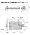
まず、本実施の形態に係るコイル基板の構造について説明する。図1は、本実施の形態に係るコイル基板を例示する図である。なお、図1(c)は平面図であり、図1(a)は図1(c)のA−A線に沿う断面図、図1(b)は図1(c)のB−B線に沿う断面図である。図2は、本実施の形態に係るコイル基板を構成する各構造体の配線の形状を模式的に例示する斜視図である。
[Structure of coil substrate]
First, the structure of the coil substrate according to the present embodiment will be described. FIG. 1 is a view illustrating a coil substrate according to the present embodiment. 1 (c) is a plan view, FIG. 1 (a) is a cross-sectional view taken along the line AA of FIG. 1 (c), and FIG. 1 (b) is a line BB of FIG. 1 (c). It is sectional drawing which follows. FIG. 2 is a perspective view schematically illustrating the shape of the wiring of each structure constituting the coil substrate according to the present embodiment.
図1及び図2を参照するに、コイル基板1は、大略すると、第1構造体1Aと、第2構造体1Bと、第3構造体1Cと、第4構造体1Dと、第5構造体1Eと、第6構造体1Fと、第7構造体1Gと、接着層501〜507と、絶縁膜70とを有する。なお、図1(c)において、絶縁層207、接着層507、及び接着層507上の絶縁膜70の図示は省略されている。又、図1(c)において、便宜上、一部の部位を梨地模様で示している。
Referring to FIG. 1 and FIG. 2, the
又、以下の説明では、適宜、製造工程を示す図を参照するものとする。又、図1では、便宜上、各開口部の符号を省略し、適宜、製造工程を示す図中の符号を参照するものとする。 In the following description, reference is made to the drawings showing the manufacturing process as appropriate. Further, in FIG. 1, for the sake of convenience, the reference numerals of the respective opening portions are omitted, and reference numerals in the drawings showing the manufacturing steps are appropriately referred to.
なお、本実施の形態では、便宜上、接着層507側を上側又は一方の側、絶縁層201側を下側又は他方の側とする。又、各部位の接着層507側の面を上面又は一方の面、絶縁層201側の面を下面又は他方の面とする。但し、コイル基板1は天地逆の状態で用いることができ、又は任意の角度で配置することができる。又、平面視とは対象物を絶縁層201の一方の面の法線方向から視ることを指し、平面形状とは対象物を絶縁層201の一方の面の法線方向から視た形状を指すものとする。
In this embodiment, for convenience, the
コイル基板1の平面形状は、例えば、コイル基板1を用いて後述のインダクタ100(図3参照)を作製した際に、インダクタ100の平面形状が1.6mm×0.8mm程度の略矩形状となる程度の大きさとすることができる。コイル基板1の厚さは、例えば、0.5mm程度とすることができる。
The planar shape of the
コイル基板1の平面形状(外縁)は、単純な矩形状ではなく、コイル基板1を構成する各配線(第7配線307等)の外縁に近い平面形状とされている。これは、コイル基板1を用いて後述のインダクタ100(図3参照)を作製した際に、コイル基板1の周囲により多くの封止樹脂110を形成するためである。又、コイル基板1の略中央部には、貫通孔1xが形成されている。これも同様に、コイル基板1を用いて後述のインダクタ100(図3参照)を作製した際に、コイル基板1の周囲により多くの封止樹脂110を形成するためである。封止樹脂110として、例えば、フェライト等の磁性体のフィラーを含有する絶縁樹脂(例えば、エポキシ系絶縁樹脂等)を用い、貫通孔1x内を含むコイル基板1の周囲のより多くの部分を封止することで、インダクタ100のインダクタンスを大きくできる。
The planar shape of the coil substrate 1 (outer edge) is not a simple rectangular shape, there is a respective wiring (
第1構造体1Aは、絶縁層201と、第1配線301と、接続部35と、絶縁層401とを有する。絶縁層201は、コイル基板1の最外層(図1では最下層)に形成されている。絶縁層201の材料としては、例えば、エポキシ系絶縁性樹脂等を用いることができる。絶縁層201の厚さは、例えば、8〜12μm程度とすることができる。
第1配線301及び接続部35は、絶縁層201上に形成されている。第1配線301及び接続部35の材料としては、例えば、銅(Cu)や銅合金等を用いることできる。第1配線301及び接続部35の厚さは、例えば、12〜50μm程度とすることができる。第1配線301の幅は、例えば、50〜130μm程度とすることができる。第1配線301はコイルの一部となる1層目の配線(約1巻)であり、図2に示す方向に略楕円形にパターニングされている。第1配線301の短手方向の断面形状は、略矩形状とすることができる。なお、渦巻きに沿う方向(Y方向)を長手方向、それに垂直な幅方向(X方向)を短手方向とする。
The
接続部35は、第1配線301の一端部に形成されている。接続部35の側面は、コイル基板1の一方の側面1yから露出しており、露出部がインダクタの電極と接続される部分となる。なお、接続部35は、第1配線301と一体に形成されている。
Connecting
絶縁層401は、第1配線301及び接続部35を被覆するように、絶縁層201上に形成されている。言い換えれば、第1構造体1Aは、絶縁層201と、絶縁層201上に形成されたコイルの一部となる第1配線301及び接続部35と、絶縁層201上に第1配線301及び接続部35を被覆して形成された絶縁層401とを備えた構造体である。但し、接続部35の側面の一部は、絶縁層401から露出している。絶縁層401は、第1配線301の上面を露出する開口部(図5の開口部4011)を備え、開口部内にはビア配線601の一部が充填され第1配線301と電気的に接続されている。絶縁層401の材料としては、例えば、感光性のエポキシ系絶縁性樹脂等を用いることができる。絶縁層401の厚さ(第1配線301の上面からの厚さ)は、例えば、5〜30μm程度とすることができる。
第2構造体1Bは、接着層501を介して、第1構造体1A上に積層されている。第2構造体1Bは、絶縁層202と、第2配線302と、絶縁層402とを有する。接着層501としては、例えば、エポキシ系接着剤又はポリイミド系接着剤等の絶縁性樹脂製の耐熱性接着剤を用いることができる。接着層501の厚さは、例えば、10〜40μm程度とすることができる。なお、絶縁層20n、絶縁層40n、及び接着層50n(nは2以上の自然数)の形状や厚さ、材料等は、特に説明しない場合には、絶縁層201、絶縁層401、及び接着層501と同様である。
なお、絶縁層20nを第1絶縁層、絶縁層40nを第2絶縁層と称する場合がある。又、絶縁層20nと絶縁層40nとは便宜上別符号としているが、何れも配線を被覆する絶縁層として機能する。そこで、絶縁層20nと絶縁層40nとを合わせて、単に絶縁層と称する場合がある。但し、接着層50nにより確実に各構造体の配線間の絶縁を確保できる場合、絶縁層40nを省くことが可能である。 The insulating layer 20n may be referred to as a first insulating layer, and the insulating layer 40n may be referred to as a second insulating layer. Further, although the insulating layer 20 n and the insulating layer 40 n have different reference numerals for convenience, they both function as an insulating layer covering the wiring. Therefore, the insulating layer 20 n and the insulating layer 40 n may be simply referred to as an insulating layer. However, in the case where the insulation between the wirings of each structure can be reliably ensured by the adhesive layer 50n, the insulating layer 40n can be omitted.
絶縁層402は、接着層501上に積層されている。第2配線302は、底面及び側面を絶縁層402に被覆され、上面を絶縁層402から露出するように形成されている。第2配線302の材料や厚さ等は、第1配線301と同様とすることができる。第2配線302はコイルの一部となる2層目の配線(1巻の約3/4)であり、図2に示す方向に略半楕円形の一部をなすようにパターニングされている。第2配線302の短手方向の断面形状は、略矩形状とすることができる。
絶縁層202は、第2配線302上及び絶縁層402上に積層されている。言い換えれば、第2構造体1Bは、絶縁層202と、絶縁層202上に形成されたコイルの一部となる第2配線302と、絶縁層202上に第2配線302を被覆して形成された絶縁層402とを備えた構造体を上下反転したものである。
Insulating
第2構造体1Bには、絶縁層202、第2配線302、及び絶縁層402を貫通する開口部が設けられ、開口部の下側は、接着層501の開口部及び絶縁層401の開口部と連通している。連通する開口部(図7の開口部1023)内にはビア配線601が充填されている。第2配線302は、ビア配線601を介して、第1配線301と直列に接続されている。又、第2構造体1Bには、絶縁層202を貫通し、第2配線302の上面を露出する開口部(図7の開口部1021)が設けられ、開口部内にはビア配線602が充填されている。第2配線302は、ビア配線602と電気的に接続されている。
The
第3構造体1Cは、接着層502を介して、第2構造体1B上に積層されている。第3構造体1Cは、絶縁層203と、第3配線303と、絶縁層403とを有する。
The third structure 1C via the
絶縁層403は、接着層502上に積層されている。第3配線303は、底面及び側面を絶縁層403に被覆され、上面を絶縁層403から露出するように形成されている。第3配線303の材料や厚さは、第1配線301と同様とすることができる。第3配線303はコイルの一部となる3層目の配線(約1巻)であり、図2に示す方向に略半楕円形にパターニングされている。第3配線303の短手方向の断面形状は、略矩形状とすることができる。
Insulating
絶縁層203は、第3配線303上及び絶縁層403上に積層されている。言い換えれば、第3構造体1Cは、絶縁層203と、絶縁層203上に形成されたコイルの一部となる第3配線303と、絶縁層203上に第3配線303を被覆して形成された絶縁層403とを備えた構造体を上下反転したものである。
Insulating
第3構造体1Cには、絶縁層203、第3配線303、及び絶縁層403を貫通し、下側が接着層502の開口部と連通する開口部が設けられ、連通する開口部(図9の開口部1033)内にはビア配線603が充填されている。ビア配線603は、第2構造体1Bの絶縁層202の開口部に形成されたビア配線602と電気的に接続されている。第3配線303は、ビア配線602及び603を介して、第2配線302と直列に接続されている。又、第3構造体1Cには、絶縁層203を貫通し、第3配線303の上面を露出する開口部(図8の開口部1031)が設けられ、開口部内にはビア配線604が充填されている。第3配線303は、ビア配線604と電気的に接続されている。
The third structure 1C, the insulating
第4構造体1Dは、接着層503を介して、第3構造体1C上に積層されている。第4構造体1Dは、絶縁層204と、第4配線304と、絶縁層404とを有する。
The
絶縁層404は、接着層503上に積層されている。第4配線304は、底面及び側面を絶縁層404に被覆され、上面を絶縁層404から露出するように形成されている。第4配線304の材料や厚さは、第1配線301と同様とすることができる。第4配線304はコイルの一部となる4層目の配線(1巻の約3/4)であり、図2に示す方向に略半楕円形の一部をなすようにパターニングされている。
Insulating
絶縁層204は、第4配線304上及び絶縁層404上に積層されている。言い換えれば、第4構造体1Dは、絶縁層204と、絶縁層204上に形成されたコイルの一部となる第4配線304と、絶縁層204上に第4配線304を被覆して形成された絶縁層404とを備えた構造体を上下反転したものである。
Insulating
第4構造体1Dには、絶縁層204、第4配線304、及び絶縁層404を貫通し、下側が接着層503の開口部と連通する開口部が設けられ、連通する開口部内にはビア配線605が充填されている。ビア配線605は、第3構造体1Cの絶縁層203の開口部に形成されたビア配線604と電気的に接続されている。第4配線304は、ビア配線604及び605を介して、第3配線303と直列に接続されている。又、第4構造体1Dには、絶縁層204を貫通し、第4配線304の上面を露出する開口部が設けられ、開口部内にはビア配線606が充填されている。第4配線304は、ビア配線606と電気的に接続されている。
The
なお、第4構造体1Dは、第2構造体1Bと同一構造であり、第2構造体1BをXY平面の法線を軸に180°回転させたものに相当する。開口部1041及び1042は夫々開口部1021及び1022に対応する。
The fourth
第5構造体1Eは、接着層504を介して、第4構造体1D上に積層されている。第5構造体1Eは、絶縁層205と、第5配線305と、絶縁層405とを有する。
絶縁層405は、接着層504上に積層されている。第5配線305は、底面及び側面を絶縁層405に被覆され、上面を絶縁層405から露出するように形成されている。第5配線305の材料や厚さは、第1配線301と同様とすることができる。第5配線305はコイルの一部となる5層目の配線(約1巻)であり、図2に示す方向に略半楕円形にパターニングされている。第5配線305の短手方向の断面形状は、略矩形状とすることができる。
Insulating
絶縁層205は、第5配線305上及び絶縁層405上に積層されている。言い換えれば、第5構造体1Eは、絶縁層205と、絶縁層205上に形成されたコイルの一部となる第5配線305と、絶縁層205上に第5配線305を被覆して形成された絶縁層405とを備えた構造体を上下反転したものである。
Insulating
第5構造体1Eには、絶縁層205、第5配線305、及び絶縁層405を貫通し、下側が接着層504の開口部と連通する開口部が設けられ、連通する開口部(図13の開口部1053)内にはビア配線607が充填されている。ビア配線607は、第4構造体1Dの絶縁層204の開口部に形成されたビア配線606と電気的に接続されている。第5配線305は、ビア配線606及び607を介して、第4配線304と直列に接続されている。又、第5構造体1Eには、絶縁層205を貫通し、第5配線305の上面を露出する開口部(図12の開口部1051)が設けられ、開口部内にはビア配線608が充填されている。第5配線305は、ビア配線608と電気的に接続されている。
The
なお、第5構造体1Eは、第3構造体1Cと同一構造であり、第3構造体1CをXY平面の法線を軸に180°回転させたものに相当する。開口部1051及び1052は夫々開口部1031及び1032に対応する。
The fifth
第6構造体1Fは、接着層505を介して、第5構造体1E上に積層されている。第6構造体1Fは、絶縁層206と、第6配線306と、絶縁層406とを有する。
絶縁層406は、接着層505上に積層されている。第6配線306は、底面及び側面を絶縁層406に被覆され、上面を絶縁層406から露出するように形成されている。第6配線306の材料や厚さは、第1配線301と同様とすることができる。第6配線306はコイルの一部となる6層目の配線(1巻の約3/4)であり、図2に示す方向に略半楕円形の一部をなすようにパターニングされている。第6配線306の短手方向の断面形状は、略矩形状とすることができる。
Insulating
絶縁層206は、第6配線306上及び絶縁層406上に積層されている。言い換えれば、第6構造体1Fは、絶縁層206と、絶縁層206上に形成されたコイルの一部となる第6配線306と、絶縁層206上に第6配線306を被覆して形成された絶縁層406とを備えた構造体を上下反転したものである。
Insulating
第6構造体1Fには、絶縁層206、第6配線306、及び絶縁層406を貫通し、下側が接着層505の開口部と連通する開口部が設けられ、連通する開口部(図14の開口部1063)内にはビア配線609が充填されている。ビア配線609は、第5構造体1Eの絶縁層205の開口部に形成されたビア配線608と電気的に接続されている。第6配線306は、ビア配線608及び609を介して、第5配線305と直列に接続されている。又、第6構造体1Fには、絶縁層206を貫通し、第6配線306の上面を露出する開口部(図14の開口部1061)が設けられ、開口部内にはビア配線6010が充填されている。第6配線306は、ビア配線6010と電気的に接続されている。
The
なお、第6構造体1Fは、便宜上別符合としているが、第2構造体1Bと同一構造であり、開口部1061及び1062は夫々開口部1021及び1022に対応する。
Incidentally, the
第7構造体1Gは、接着層506を介して、第6構造体1F上に積層されている。第7構造体1Gは、絶縁層207と、第7配線307と、接続部37と、絶縁層407とを有する。
The
絶縁層407は、接着層506上に積層されている。第7配線307及び接続部37は、底面及び側面を絶縁層407に被覆され、上面を絶縁層407から露出するように形成されている。第7配線307及び接続部37の材料や厚さは、第1配線301と同様とすることができる。第7配線307は最上層の配線であり、図2に示す方向に略半楕円形にパターニングされている。
Insulating
接続部37は、第7配線307の一端部に形成されている。接続部37の側面は、コイル基板1の他方の側面1zから露出しており、露出部がインダクタの電極と接続される部分となる。なお、接続部37は、第7配線307と一体に形成されている。絶縁層207は、第7配線307上、接続部37上、及び絶縁層407上に積層されている。言い換えれば、第7構造体1Gは、絶縁層207と、絶縁層207上に形成された第7配線307及び接続部37と、絶縁層207上に第7配線307及び接続部37を被覆して形成された絶縁層407とを備えた構造体を上下反転したものである。
Connecting
第7構造体1Gには、絶縁層207、第7配線307、及び絶縁層407を貫通し、下側が接着層506の開口部と連通する開口部が設けられ、連通する開口部(図16の開口部1072)内にはビア配線6011が充填されている。ビア配線6011は、第6構造体1Fの絶縁層206の開口部に形成されたビア配線6010と電気的に接続されている。第7配線307は、ビア配線6010及び6011を介して、第6配線306と直列に接続されている。このように、コイル基板1では、隣接する構造体の配線同士を直列に接続して、接続部35から接続部37に至る螺旋状のコイルを形成している。
The
接着層507は、第7構造体1G上に積層されている。接着層507には、開口部は形成されていない。つまり、第1構造体1Aから第7構造体1Gが積層された積層体の上側は、絶縁層である接着層507に被覆されており、導電体は露出していない。
第1構造体1Aから第7構造体1Gが積層された積層体において、底面並びに側面1y及び1zを除く表面は絶縁膜70に被覆されている。貫通孔1xの内壁面も絶縁膜70に被覆されている。絶縁膜70は、積層体から露出する各配線の端面が、インダクタ100(図3参照)を作製した際に、封止樹脂110に含有される場合がある導電体(磁性体のフィラー等)と短絡することを防止するために設ける。絶縁膜70としては、例えば、エポキシ系やアクリル系絶縁性樹脂等を用いることができる。絶縁膜70は、シリカ等のフィラーを含有しても構わない。絶縁膜70の厚さは、例えば、20〜50μm程度とすることができる。
In the laminated body in which the first
図3は、本実施の形態に係るインダクタを例示する断面図である。図3を参照するに、インダクタ100は、コイル基板1を封止樹脂110で封止し、電極120及び130を形成したチップインダクタである。インダクタ100の平面形状は、例えば、1.6mm×0.8mm程度の略矩形状とすることができる。インダクタ100の厚さは、例えば、1.0mm程度とすることができる。インダクタ100は、例えば、小型の電子機器の電圧変換回路等に用いることができる。
FIG. 3 is a cross-sectional view illustrating an inductor according to the present embodiment. Referring to FIG. 3, the
インダクタ100において、封止樹脂110は、コイル基板1の一方の側面1y及び他方の側面1zを除く部分を封止している。つまり、封止樹脂110は、コイル基板1の接続部35及び37が露出する側面の一部を除いてコイル基板1を被覆している。なお、封止樹脂110は、貫通孔1x内にも形成されている。封止樹脂110としては、例えば、フェライト等の磁性体のフィラーを含有する絶縁樹脂(例えば、エポキシ系絶縁樹脂等)を用いることができる。磁性体は、インダクタ100のインダクタンスを大きくする機能を有する。
In the
このように、コイル基板1には貫通孔1xが形成されており、貫通孔1xも磁性体を含有するエポキシ系絶縁樹脂等の絶縁樹脂で充填されるため、インダクタンスをより向上できる。貫通孔1x内に、フェライト等の磁性体のコアを配置し、コアを含めて封止樹脂110を形成してもよい。コアの形状は、例えば、円柱状や直方体状等とすることができる。
As described above, the through
電極120は、封止樹脂110の外側に形成され、接続部35の一部と電気的に接続されている。具体的には、電極120は、封止樹脂110の一方の側面、並びに上面及び下面の一部に連続的に形成されている。電極120の内壁面は、コイル基板1の一方の側面1yから露出する接続部35の側面と接し、両者は電気的に接続されている。
The
電極130は、封止樹脂110の外側に形成され、接続部37の一部と電気的に接続されている。具体的には、電極130は、封止樹脂110の他方の側面、並びに上面及び下面の一部に連続的に形成されている。電極130の内壁面は、コイル基板1の他方の側面1zから露出する接続部37の側面と接し、両者は電気的に接続されている。電極120及び130の材料としては、例えば、銅(Cu)や銅合金等を用いることができる。電極120及び130は、例えば、銅ペーストの塗布、銅のスパッタ、又は無電解めっき等により形成することができる。なお、電極120及び130は、複数の金属層を積層した構造としてもよい。
The
[コイル基板の製造方法]
次に、本実施の形態に係るコイル基板の製造方法について説明する。図4〜図21は、本実施の形態に係るコイル基板の製造工程を例示する図である。まず、図4に示す工程について説明する。図4(a)は平面図であり、図4(b)は図4(a)の1つの個別領域C(後述)の近傍についての図4(a)のYZ平面に平行な方向の断面を示している。図4に示す工程では、まず、基板101(第1基板)として例えばリール状(テープ状)の可撓性を有する絶縁樹脂フィルムを準備する。
[Method of manufacturing coil substrate]
Next, a method of manufacturing a coil substrate according to the present embodiment will be described. 4 to 21 are diagrams illustrating the manufacturing process of the coil substrate according to the present embodiment. First, the process shown in FIG. 4 will be described. 4 (a) is a plan view, and FIG. 4 (b) is a cross section in the direction parallel to the YZ plane of FIG. 4 (a) for the vicinity of one individual area C (described later) in FIG. 4 (a). It shows. In the process shown in FIG. 4, first, an insulating resin film having flexibility, for example, in the form of a reel (tape) is prepared as a substrate 10 1 (first substrate).
そして、プレス加工法等により、基板101の短手方向(図中の縦(Y)方向)の両端部に、スプロケットホール10zを、基板101の長手方向(図中の横(X)方向)に沿って略一定間隔で連続的に形成する。その後、スプロケットホール10zが形成された基板101の両端部を除く領域において、基板101の一方の面に絶縁層201及び金属箔3001を順次積層する。具体的には、例えば、基板101の一方の面に半硬化状態の絶縁層201及び金属箔3001を順次積層し、加熱して半硬化状態の絶縁層201を硬化させる。
Then, by press working method or the like, on both ends of the widthwise direction of the substrate 10 1 (vertical in FIG. (Y) direction), the
スプロケットホール10zが形成された基板101の両端部の内側の点線で示した複数の領域Cは、最終的に点線に沿って切断されて個片化され、各々がコイル基板1となる領域(以降、個別領域Cとする)である。複数の個別領域Cは、例えば、縦横に配列することができる。その際、複数の個別領域Cは、図4(a)に示すように所定の間隔を介して配列されてもよいし、互いに接するように配列されてもよい。又、個別領域Cの数やスプロケットホール10zの数は、任意に決定できる。なお、Dは、後工程でリール状(テープ状)の基板101等を切断してシート状とするための切断位置(以降、切断位置Dとする)を示している。
A plurality of regions C shown inside the dotted line at both ends of the
基板101としては、例えば、ポリフェニレンサルファイドフィルムやポリイミドフィルム、ポリエチレンナフタレートフィルム等を用いることができる。基板101の厚さは、例えば、50〜75μm程度とすることができる。
As the
絶縁層201としては、例えば、フィルム状のエポキシ系絶縁性樹脂等を用いることができる。或いは、絶縁層201として、液状又はペースト状のエポキシ系絶縁性樹脂等を用いてもよい。絶縁層201の厚さは、例えば、8〜12μm程度とすることができる。金属箔3001は、パターニングされて金属層3011及び接続部35となる部位であり、例えば、銅箔を用いることができる。金属箔3001の厚さは、例えば、12〜50μm程度とすることができる。
As the insulating
なお、スプロケットホール10zは、コイル基板1を作製する過程で基板101が各種製造装置等に装着された際、モータ等により駆動されるスプロケットのピンと噛み合って、基板101をピッチ送りするための貫通孔である。基板101の幅(スプロケットホール10zの配列方向に垂直な方向(Y方向))は、基板101が装着される製造装置に対応するように決定される。
Incidentally,
基板101の幅は、例えば、40〜90mm程度とすることができる。一方、基板101の長さ(スプロケットホール10zの配列方向(X方向))は、任意に決定することができる。図4(a)では、個別領域Cは5行10列とされている。しかし、基板101をより長くして個別領域Cを例えば数100列程度とすることも可能である。
The width of the
次に、図5に示す工程(図5(b)は平面図、図5(a)は図5(b)のA−A線に沿う断面図)では、基板101上に、金属層3011が形成された第1構造体1Aを作製する。金属層3011は、最終的に成形(型抜き等)されて、コイルの一部となる1層目の配線(約1巻)である第1配線301となる部分である。 具体的には、図4(b)に示す金属箔3001をパターニングして、絶縁層201上に金属層3011形成する。又、金属層3011の一端部に接続部35を形成する。又、接続部35に接続するバスライン36を形成する。バスライン36は後工程において電解めっきの給電に使用するものであり、各個別領域Cの金属層3011及び接続部35と電気的に接続される。なお、後工程において電解めっきを行わない場合にはバスライン36は形成しなくてもよい。金属層3011には切れ込み部301xが形成されている。切れ込み部301xは、後工程でコイル基板を成形(型抜き等)する際に、コイルを構成する渦巻き形状を形成しやすくするために設けるものである。
Next, the step (FIG. 5 (b) a plan view, FIG. 5 (a) is a cross-sectional view taken along the line A-A of FIG. 5 (b)) shown in FIG. 5, on the
金属箔3001のパターニングは、例えば、フォトリソグラフィ法により行うことができる。すなわち、金属箔3001上に感光性のレジストを塗布し、所定の領域を露光及び現像してレジストに開口部を形成し、開口部内に露出する金属箔3001をエッチングで除去することでパターニングできる。なお、金属層3011、接続部35、及びバスライン36は一体に形成されている。
Patterning of the
その後、金属層3011、接続部35、及びバスライン36を絶縁層401で被覆する。絶縁層401は、例えば、フィルム状の感光性のエポキシ系絶縁性樹脂等をラミネートすることで形成できる。或いは、液状又はペースト状の感光性のエポキシ系絶縁性樹脂等を塗布することで形成してもよい。絶縁層401の厚さ(金属層3011の上面からの厚さ)は、例えば、5〜30μm程度とすることができる。
Thereafter, the
その後、第1構造体1Aの絶縁層401に、金属層3011の上面を露出する開口部4011を形成する。開口部4011の平面形状は、例えば、直径150μm程度の円形状とすることができる。開口部4011は、例えば、プレス加工法やレーザ加工法等により形成できる。開口部4011は、感光性の絶縁層401の露光及び現像で形成してもよい。なお、図5(b)において、絶縁層401の図示は省略されている。又、図5(b)において、金属層3011の開口部4011に対応する領域を破線で示している。
Thereafter, the insulating
次に、図6に示す工程(図6(b)は平面図、図6(a)は図6(b)のA−A線に沿う断面図)では、基板102(第2基板)上に、金属層3012が形成された第2構造体1Bを作製する。金属層3012は、最終的に成形(型抜き等)されて、コイルの一部となる2層目の配線(1巻の約3/4)である第2配線302となる部分である。具体的には、図4に示す工程と同様にして、基板102にスプロケットホール10zを形成後、スプロケットホール10zが形成された基板102の両端部を除く領域において、基板102上に絶縁層202及び金属箔3002(図示せず)を順次積層する。
Next, the step (FIG. 6 (b) a plan view, FIG. 6 (a) 6 (sectional view taken along line A-A of b)) shown in FIG. 6, the substrate 10 2 (second substrate) on to, to prepare a
そして、図5に示す工程と同様にして金属箔3002をパターニングし、絶縁層202上に、図6(b)に示すようにパターニングされた金属層3012を形成する。その後、金属層3012を絶縁層402で被覆する。そして、基板102及び第2構造体1Bの絶縁層202に、金属層3012の下面を露出する開口部1021を形成する。又、基板102、第2構造体1Bの絶縁層202、金属層3012、及び絶縁層402を貫通する開口部1022(貫通孔)を形成する。
Then, in the same manner as in the step shown in FIG. 5 by patterning the
開口部1021及び1022の夫々の平面形状は、例えば、直径150μm程度の円形状とすることができる。開口部1021及び1022は、例えば、プレス加工法やレーザ加工法等により形成できる。開口部1022は、第1構造体1Aと第2構造体1Bが所定方向に積層された際に開口部4011と平面視で重複する位置に形成する。なお、図6(b)において、絶縁層402の図示は省略されている。又、図6(b)において、金属層3012の開口部1021に対応する領域を破線で示している。
The planar shape of each of the openings 10 21 and 10 22 may be, for example, a diameter 150μm approximately circular shape. Openings 10 21 and 10 22, for example, be formed by pressing method or a laser processing method or the like.
なお、基板10n及び金属箔300n(nは2以上の自然数)の形状や厚さ、材料等は、特に説明しない場合には、基板101及び金属箔3001と同様である。
The shape and thickness of the substrate 10n and the metal foil 300 n (n is a natural number of 2 or more), the material or the like, if not particularly described are the same as the
次に、図7(a)〜図7(c)に示す工程について説明する。なお、図7(a)〜図7(c)は、図6(a)に対応する断面図である。まず、図7(a)に示す工程では、接着層501を準備し、接着層501を貫通する開口部5011(貫通孔)を形成する。開口部5011は、第1構造体1Aと第2構造体1Bが接着層501を介して所定方向に積層された際に開口部4011及び1022と平面視で重複する位置に形成する。接着層501としては、例えば、エポキシ系接着剤又はポリイミド系接着剤等の絶縁性樹脂製の耐熱性接着剤(熱硬化性)を用いることができる。接着層501の厚さは、例えば、10〜40μm程度とすることができる。
Next, steps shown in FIG. 7A to FIG. 7C will be described. 7 (a) to 7 (c) are cross-sectional views corresponding to FIG. 6 (a). In the step shown in FIG. 7 (a), to prepare an
次に、基板102及び第2構造体1Bを図6に示す状態から反転させ、接着層501を介して、第1構造体1A上に積層する。つまり、第1構造体1Aと第2構造体1Bとを、接着層501を介して、対向配置し、基板101と基板102が外側になるように積層する。その後、接着層501を硬化させる。このとき、開口部4011、開口部5011、及び開口部1022が連通して1つの開口部1023が形成され、底部に金属層3011の上面が露出する。
Next, the
但し、図6及び図7(a)に示す工程において、各開口部を設ける前に第2構造体1Bを接着層501を介して第1構造体1A上に積層し、その後、開口部1021、1022、及び5011を設けてもよい。
However, in the step shown in FIG. 6 and FIG. 7 (a), stacking a
次に、図7(b)に示す工程では、基板102を第2構造体1Bの絶縁層202から除去(剥離)する。例えば、基板102は第2構造体1Bの絶縁層202から機械的に剥離できる。
Next, in a step shown in FIG. 7 (b), removing the
次に、図7(c)に示す工程では、開口部1023の底部に露出する金属層3011上に、例えば銅(Cu)等からなるビア配線601を形成する。金属層3011と金属層3012とは、ビア配線601を介して直列に接続される。又、開口部1021の底部に露出する金属層3012上に、例えば銅(Cu)等からなるビア配線602を形成する。金属層3012とビア配線602とは電気的に接続される。
Next, in a step shown in FIG. 7 (c), on the
ビア配線601及び602は、例えば、金属層3011及び3012側から夫々バスライン36を給電に使用する電解めっき法により銅(Cu)等を析出させることで形成できる。又、ビア配線601及び602は、例えば、開口部1023の底部に露出する金属層3011上に銅(Cu)等の金属ペーストを充填し、開口部1021の底部に露出する金属層3012上に銅(Cu)等の金属ペーストを充填して形成してもよい。ビア配線601及び602の夫々の上面は、絶縁層202の上面と略面一とすることができる。この工程により、第1構造体1A上に第2構造体1Bが積層された積層体において、金属層3011、ビア配線601、及び金属層3012が直列に接続される。この直列に接続された部分は、最終的に成形(型抜き等)されて約1巻きと3/4のコイルとなる。
Via
次に、図8に示す工程では、図6に示す工程と同様にして、基板103上に、金属層3013が形成された第3構造体1Cを作製する。なお、図8(c)は平面図、図8(a)は図8(c)のA−A線に沿う断面図、図8(b)は図8(c)のE−E線に沿う断面図である。金属層3013は、最終的に成形(型抜き等)されて、コイルの一部となる3層目の配線(約1巻)である第3配線303となる部分である。金属層3013には切れ込み部301yが形成されている。切れ込み部301yは、後工程でコイル基板を成形(型抜き等)する際に、コイルを構成する渦巻き形状を形成しやすくするために設けるものである。
Then, in the process shown in FIG. 8, similarly to the step shown in FIG. 6, on the substrate 103 to produce a third structure 1C in which the
次に、基板103及び第3構造体1Cの絶縁層203に、金属層3013の下面を露出する開口部1031を形成する。又、基板103、第3構造体1Cの絶縁層203、金属層3013、及び絶縁層403を貫通する開口部1032(貫通孔)を形成する。
Next, the insulating
開口部1031及び1032の平面形状や加工法は、例えば、開口部1021等と同様とすることができる。開口部1032は、第2構造体1Bと第3構造体1Cが所定方向に積層された際に開口部1021と平面視で重複する位置に形成する。なお、図8(c)において、絶縁層403の図示は省略されている。又、図8(c)において、金属層3013の開口部1031に対応する領域を破線で示している。
The planar shape and working method of the openings 10 31 and 10 32, for example, may be similar to the openings 10 21 and the like.
次に、図9(a)〜図9(c)に示す工程について説明する。なお、図9(a)〜図9(c)は、図7(a)に対応する断面図である。まず、図9(a)に示す工程では、接着層502を準備し、接着層502を貫通する開口部5021(貫通孔)を形成する。開口部5021は、第2構造体1Bと第3構造体1Cが接着層502を介して所定方向に積層された際にビア配線602と平面視で重複する位置に形成する。なお、接着層50n(nは2以上の自然数)の形状や厚さ、材料等は、特に説明しない場合には、接着層501と同様である。
Next, steps shown in FIG. 9A to FIG. 9C will be described. 9 (a) to 9 (c) are cross-sectional views corresponding to FIG. 7 (a). In the step shown in FIG. 9 (a), to prepare the
次に、基板103及び第3構造体1Cを図8に示す状態から反転させ、接着層502を介して、第2構造体1B上に積層する。つまり、第2構造体1Bと第3構造体1Cとを、接着層502を介して、対向配置し、基板101と基板103が外側になるように積層する。その後、接着層502を硬化させる。このとき、開口部5021及び開口部1032が連通して1つの開口部1033が形成され、底部にビア配線602の上面が露出する。
Next, the substrate 103 and the third structural member 1C is reversed from the state shown in FIG. 8, via the
但し、図8及び図9(a)に示す工程において、各開口部を設ける前に第3構造体1Cを接着層502を介して第2構造体1B上に積層し、その後、開口部1031、1032、及び5021を設けてもよい。
However, in the step shown in FIG. 8 and FIG. 9 (a), stacked on the
次に、図9(b)に示す工程では、基板103を第3構造体1Cの絶縁層203から除去(剥離)する。
Then, in the process shown in FIG. 9 (b), the
次に、図9(c)に示す工程では、開口部1033の底部に露出するビア配線602上にビア配線603を形成する。金属層3012と金属層3013とは、ビア配線602及び603を介して直列に接続される。又、開口部1031(図示せず)の底部に露出する金属層3013上にビア配線604(図示せず)を形成する。金属層3013とビア配線604とは電気的に接続される。
Then, in the process shown in FIG. 9 (c), to form the via wirings 60 3 on the via
ビア配線603及び604は、例えば、ビア配線601等と同様に、バスライン36を給電に使用する電解めっき法や金属ペーストの充填により形成できる。ビア配線603及び604の材料としては、例えば、銅(Cu)等を用いることができる。ビア配線603及び604の夫々の上面は、絶縁層203の上面と略面一とすることができる。この工程により、第1構造体1Aから第3構造体1Cが積層された積層体において、金属層3011、3012、及び3013がビア配線を介して直列に接続される。この直列に接続された部分は、最終的に成形(型抜き等)されて約2巻きと3/4のコイルとなる。
Via
次に、図10に示す工程(図10(b)は平面図、図10(a)は図10(b)のF−F線に沿う断面図)では、図6に示す工程と同様にして、基板104上に、金属層3014が形成された第4構造体1Dを作製する。金属層3014は、最終的に成形(型抜き等)されて、コイルの一部となる4層目の配線(1巻の約3/4)である第4配線304となる部分である。
Next, in the step shown in FIG. 10 (FIG. 10 (b) is a plan view, and FIG. 10 (a) is a cross-sectional view taken along the line F-F in FIG. 10 (b)). , on the substrate 104 to produce a
次に、基板104及び第4構造体1Dの絶縁層204に、金属層3014の下面を露出する開口部1041を形成する。又、基板104、第4構造体1Dの絶縁層204、金属層3014、及び絶縁層404を貫通する開口部1042(貫通孔)を形成する。
Next, the insulating
開口部1041及び1042の平面形状や加工法は、例えば、開口部1021等と同様とすることができる。開口部1042は、第3構造体1Cと第4構造体1Dが所定方向に積層された際にビア配線604と平面視で重複する位置に形成する。なお、図10(b)において、絶縁層404の図示は省略されている。又、図10(b)において、金属層3014の開口部1041に対応する領域を破線で示している。
The planar shape and working method of the openings 10 41 and 10 42, for example, may be similar to the openings 10 21 and the like.
次に、図11(a)〜図11(c)に示す工程について説明する。なお、図11(a)〜図11(c)は、図10(a)に対応する断面図である。まず、図11(a)に示す工程では、接着層503を準備し、接着層503を貫通する開口部5031(貫通孔)を形成する。開口部5031は、第3構造体1Cと第4構造体1Dが接着層503を介して所定方向に積層された際にビア配線604と平面視で重複する位置に形成する。
Next, steps shown in FIGS. 11A to 11C will be described. 11 (a) to 11 (c) are cross-sectional views corresponding to FIG. 10 (a). In the step shown in FIG. 11 (a), to prepare an
次に、基板104及び第4構造体1Dを図10に示す状態から反転させ、接着層503を介して、第3構造体1C上に積層する。つまり、第3構造体1Cと第4構造体1Dとを、接着層503を介して、対向配置し、基板101と基板104が外側になるように積層する。その後、接着層503を硬化させる。このとき、開口部5031及び開口部1042が連通して1つの開口部1043が形成され、底部にビア配線604の上面が露出する。
Next, the substrate 104 and the
但し、図10及び図11(a)に示す工程において、各開口部を設ける前に第4構造体1Dを接着層503を介して第3構造体1C上に積層し、その後、開口部1041、1042、及び5031を設けてもよい。
However, in the step shown in FIG. 10 and FIG. 11 (a), stacking a
次に、図11(b)に示す工程では、基板104を第4構造体1Dの絶縁層204から除去(剥離)する。
Next, in a step shown in FIG. 11 (b), removing the substrate 104 from the insulating
次に、図11(c)に示す工程では、開口部1043の底部に露出するビア配線604上にビア配線605を形成する。金属層3013と金属層3014とは、ビア配線604及び605を介して直列に接続される。又、開口部1041の底部に露出する金属層3014上にビア配線606を形成する。金属層3014とビア配線606とは電気的に接続される。
Next, in a step shown in FIG. 11 (c), to form the via wirings 60 5 on the via
ビア配線605及び606は、例えば、ビア配線601等と同様に、バスライン36を給電に使用する電解めっき法や金属ペーストの充填により形成できる。ビア配線605及び605の材料としては、例えば、銅(Cu)等を用いることができる。ビア配線605及び606の夫々の上面は、絶縁層204の上面と略面一とすることができる。この工程により、第1構造体1Aから第4構造体1Dが積層された積層体において、金属層3011、3012、3013、及び3014がビア配線を介して直列に接続される。この直列に接続された部分は、最終的に成形(型抜き等)されて約3巻きのコイルとなる。
Via
次に、図12に示す工程では、図6に示す工程と同様にして、基板105上に、金属層3015が形成された第5構造体1Eを作製する。なお、図12(c)は平面図、図12(a)は図12(c)のF−F線に沿う断面図、図21(b)は図12(c)のG−G線に沿う断面図である。金属層3015は、最終的に成形(型抜き等)されて、コイルの一部となる5層目の配線(約1巻)である第5配線305となる部分である。金属層3015には切れ込み部301yが形成されている。切れ込み部301yは、後工程でコイル基板を成形(型抜き等)する際に、コイルを構成する渦巻き形状を形成しやすくするために設けるものである。
Next, in a step shown in FIG. 12, in the same manner as in the step shown in FIG. 6, on the substrate 105 to produce a
次に、基板105及び第5構造体1Eの絶縁層205に、金属層3015の下面を露出する開口部1051を形成する。又、基板105、第5構造体1Eの絶縁層205、金属層3015、及び絶縁層405を貫通する開口部1052(貫通孔)を形成する。
Next, the insulating
開口部1051及び1052の平面形状や加工法は、例えば、開口部1021等と同様とすることができる。開口部1052は、第4構造体1Dと第5構造体1Eが所定方向に積層された際に開口部5041と平面視で重複する位置に形成する。なお、図12(c)において、絶縁層405の図示は省略されている。又、図12(c)において、金属層3015の開口部1051に対応する領域を破線で示している。
The planar shape and working method of the openings 10 51 and 10 52, for example, may be similar to the openings 10 21 and the like.
次に、図13(a)〜図13(c)に示す工程について説明する。なお、図13(a)〜図13(c)は、図12(a)に対応する断面図である。まず、図13(a)に示す工程では、接着層504を準備し、接着層504を貫通する開口部5041(貫通孔)を形成する。開口部5041は、第4構造体1Dと第5構造体1Eが接着層504を介して所定方向に積層された際にビア配線606と平面視で重複する位置に形成する。
Next, steps shown in FIG. 13A to FIG. 13C will be described. 13 (a) to 13 (c) are cross-sectional views corresponding to FIG. 12 (a). In the step shown in FIG. 13 (a), to prepare an
次に、基板105及び第5構造体1Eを図12に示す状態から反転させ、接着層504を介して、第4構造体1D上に積層する。つまり、第4構造体1Dと第5構造体1Eとを、接着層504を介して、対向配置し、基板101と基板105が外側になるように積層する。その後、接着層504を硬化させる。このとき、開口部5041及び開口部1052が連通して1つの開口部1053が形成され、底部にビア配線606の上面が露出する。
Next, the substrate 105 and the
但し、図12及び図13(a)に示す工程において、各開口部を設ける前に第5構造体1Eを接着層504を介して第4構造体1D上に積層し、その後、開口部1051、1052、及び5041を設けてもよい。
However, in the step shown in FIG. 12 and FIG. 13 (a), the laminated
次に、図13(b)に示す工程では、基板105を第5構造体1Eの絶縁層205から除去(剥離)する。
Next, in a step shown in FIG. 13 (b), the substrate 105 is removed from the insulating
次に、図13(c)に示す工程では、開口部1053の底部に露出するビア配線606上にビア配線607を形成する。金属層3015と金属層3014とは、ビア配線606及び607を介して直列に接続される。又、開口部1051(図示せず)の底部に露出する金属層3015上にビア配線608(図示せず)を形成する。金属層3015とビア配線608とは電気的に接続される。
Next, in a step shown in FIG. 13 (c), to form the via wirings 60 7 on the via wirings 60 6 exposed at the bottom of the opening 10 53.
ビア配線607及び608は、例えば、ビア配線601等と同様に、バスライン36を給電に使用する電解めっき法や金属ペーストの充填により形成できる。ビア配線607及び608の材料としては、例えば、銅(Cu)等を用いることができる。ビア配線607及び608の夫々の上面は、絶縁層205の上面と略面一とすることができる。この工程により、第1構造体1Aから第5構造体1Eが積層された積層体において、金属層3011、3012、3013、3014、及び3015がビア配線を介して直列に接続される。この直列に接続された部分は、最終的に成形(型抜き等)されて約4巻きのコイルとなる。
Via
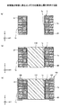
次に、図14(a)〜図14(c)に示す工程について説明する。なお、図14(a)〜図14(c)は、図7(a)に対応する断面図である。まず、図14(a)に示す工程では、基板106上に、金属層3016が形成された第6構造体1Fを作製する。金属層3016は、最終的に成形(型抜き等)されて、コイルの一部となる6層目の配線(1巻の約3/4)である第6配線306となる部分である。そして、基板106及び第6構造体1Fの絶縁層206に、金属層3016の下面を露出する開口部1061を形成する。又、基板106、第6構造体1Fの絶縁層206、金属層3016、及び絶縁層406を貫通する開口部1062(貫通孔)を形成する。なお、第6構造体1Fは、便宜上別符合としているが、図6に示す第2構造体1Bと同一構造であり、開口部1061及び1062は夫々開口部1021及び1022に対応する。
Next, steps shown in FIGS. 14 (a) to 14 (c) will be described. 14 (a) to 14 (c) are cross-sectional views corresponding to FIG. 7 (a). In the step shown in FIG. 14 (a), on a substrate 106 to produce a
次に、接着層505を準備し、接着層505を貫通する開口部5051(貫通孔)を形成する。開口部5051は、第6構造体1Fと第5構造体1Eが接着層505を介して所定方向に積層された際にビア配線608と平面視で重複する位置に形成する。そして、図7(a)と同様にして、基板106及び第6構造体1Fを図6に示す状態から反転させ、接着層505を介して、第5構造体1E上に積層する。つまり、第5構造体1Eと第6構造体1Fとを、接着層505を介して、対向配置し、基板101と基板106が外側になるように積層する。その後、接着層505を硬化させる。このとき、開口部5051及び開口部1062が連通して1つの開口部1063が形成され、底部にビア配線608の上面が露出する。
Next, prepare the
但し、図6及び図14(a)に示す工程において、各開口部を設ける前に第6構造体1Fを接着層505を介して第5構造体1E上に積層し、その後、開口部1061、1062、及び5051を設けてもよい。
However, in the step shown in FIG. 6 and FIG. 14 (a), the laminated
次に、図14(b)に示す工程では、基板106を第6構造体1Fの絶縁層206から除去(剥離)する。
Next, in a step shown in FIG. 14 (b), removing the substrate 106 from the insulating
次に、図14(c)に示す工程では、開口部1063の底部に露出するビア配線608上にビア配線609を形成する。金属層3015と金属層3016とは、ビア配線608及び609を介して直列に接続される。又、開口部1061の底部に露出する金属層3016上にビア配線6010を形成する。金属層3016とビア配線6010とは電気的に接続される。
Next, in a step shown in FIG. 14 (c), to form a via
ビア配線609及び6010は、例えば、ビア配線601等と同様に、バスライン36を給電に使用する電解めっき法や金属ペーストの充填により形成できる。ビア配線609及び6010の材料としては、例えば、銅(Cu)等を用いることができる。ビア配線609及び6010の夫々の上面は、絶縁層206の上面と略面一とすることができる。この工程により、第1構造体1Aから第6構造体1Fが積層された積層体において、金属層3011、3012、3013、3014、3015、及び3016がビア配線を介して直列に接続される。この直列に接続された部分は、最終的に成形(型抜き等)されて約4巻きと3/4のコイルとなる。
Via
次に、図15に示す工程では、図6に示す工程と同様にして、基板107上に、金属層3017が形成された第7構造体1Gを作製する。金属層3017は、最終的に成形(型抜き等)されて、コイルの一部となる7層目の配線(約1巻)である第7配線307となる部分である。具体的には、絶縁層207上に金属層3017を形成する。又、金属層3017の一端部に接続部37を形成する。なお、金属層3017及び接続部37は一体に形成されている。金属層3017には切れ込み部301xが形成されている。切れ込み部301xは、後工程でコイル基板を成形(型抜き等)する際に、コイルを構成する渦巻き形状を形成しやすくするために設けるものである。
Then, in the process shown in FIG. 15, in the same manner as in the step shown in FIG. 6, on the substrate 107 to produce a
次に、基板107、第7構造体1Gの絶縁層207、金属層3017、及び絶縁層407を貫通する開口部1072(貫通孔)を形成する。なお、図15(b)は平面図、図15(a)は図15(b)のA−A線に沿う断面図である。開口部1072の平面形状や加工法は、例えば、開口部1021等と同様とすることができる。開口部1072は、第6構造体1Eと第7構造体1Gが所定方向に積層された際にビア配線6010と平面視で重複する位置に形成する。なお、図15(b)において、絶縁層407の図示は省略されている。
Next, a substrate 107, an insulating
次に、図16(a)〜図16(c)に示す工程について説明する。なお、図16(a)〜図16(c)は、図15(a)に対応する断面図である。まず、図16(a)に示す工程では、接着層506を準備し、接着層506を貫通する開口部5061(貫通孔)を形成する。開口部5061は、第6構造体1Fと第7構造体1Gが接着層506を介して所定方向に積層された際にビア配線6010と平面視で重複する位置に形成する。
Next, the steps shown in FIGS. 16 (a) to 16 (c) will be described. 16 (a) to 16 (c) are cross-sectional views corresponding to FIG. 15 (a). In the step shown in FIG. 16 (a), to prepare an
次に、基板107及び第7構造体1Gを図15に示す状態から反転させ、接着層506を介して、第6構造体1F上に積層する。つまり、第6構造体1Fと第7構造体1Gとを、接着層506を介して、対向配置し、基板101と基板107が外側になるように積層する。その後、接着層506を硬化させる。このとき、開口部5061及び開口部1072が連通して1つの開口部1073が形成され、底部にビア配線6010の上面が露出する。
Next, the substrate 107 and the
但し、図15及び図16(a)に示す工程において、各開口部を設ける前に第7構造体1Gを接着層506を介して第6構造体1F上に積層し、その後、開口部1072及び5061を設けてもよい。
However, in the step shown in FIG. 15 and FIG. 16 (a), the laminated on the
次に、図16(b)に示す工程では、基板107を第7構造体1Gの絶縁層207から除去(剥離)する。
Next, in a step shown in FIG. 16 (b), removing the substrate 107 from the insulating
次に、図16(c)に示す工程では、開口部1073の底部に露出するビア配線6010上にビア配線6011を形成する。金属層3016と金属層3017とは、ビア配線6010及び6011を介して直列に接続される。
Next, in a step shown in FIG. 16 (c), to form a via wiring 60 11 on the via wirings 60 10 exposed at the bottom of the opening 10 73.
ビア配線6011は、例えば、ビア配線601等と同様に、バスライン36を給電に使用する電解めっき法や金属ペーストの充填により形成できる。ビア配線6011の材料としては、例えば、銅(Cu)等を用いることができる。ビア配線6011の上面は、絶縁層207の上面と略面一とすることができる。この工程により、第1構造体1Aから第7構造体1Gが積層された積層体において、金属層3011、3012、3013、3014、3015、3016、及び3017がビア配線を介して直列に接続される。この直列に接続された部分は、最終的に成形(型抜き等)されて約5巻きと1/2のコイルとなる。
Via
次に、図17(a)に示す工程では、第7構造体1G上に、開口部が形成されていない接着層507を積層する。次に、図17(b)に示す工程では、図17(a)に示す構造体を、図4に示す切断位置Dで切断して個片化し、シート状の基板1Mとする。図17の例では、基板1Mには、50個の個別領域Cが形成されている。但し、図17(b)に示す工程を実行せず、図21に示す工程が終了したリール状(テープ状)の構造体を、そのまま製品として出荷してもよい。
Next, in the step shown in FIG. 17 (a), on the
次に、図18〜図21(a)に示す工程では、基板1Mを成形(型抜き等)して不要部分を除去し、各層に形成された金属層を螺旋状のコイルの一部を構成する形状の配線にする。図18は、基板1Mを成形(型抜き等)する前の金属層3017を例示する平面図である(金属層3017よりも上層の図示は省略)。図19は、基板1Mを成形(型抜き等)する前の各層に形成された金属層の形状を模式的に例示する斜視図である。図18及び図19に示した各金属層が形成された基板1Mを金型を用いたプレス加工法等により成形し、図20及び図21(a)に示す形状とする。なお、図20は図18に対応する平面図、図21(a)は図20のA−A線に沿う断面図である。なお、図20及び図21(a)に示す構造体の各層の配線の形状は、図2のようになる。基板1Mを金型を用いたプレス加工法等に代えて、レーザ加工法等により成形してもよい。
Next, in the steps shown in FIGS. 18 to 21A, the
この工程により、第1構造体1Aから第7構造体1Gが積層された積層体において、金属層3011が成形されて第1配線301となる。同様に、金属層3012、3013、3014、3015、3016、及び3017が成形されて、夫々第2配線302、第3配線303、第4配線304、第5配線305、第6配線306、及び第7配線307となる。第1配線301、第2配線302、第3配線303、第4配線304、第5配線305、第6配線306、及び第7配線307はビア配線を介して直列に接続された、約5巻きと1/2の螺旋状のコイルである。
This step in the laminate from the
なお、第1構造体1Aから第7構造体1Gが積層された積層体は各個別領域Cに形成され、隣接する個別領域C間に形成された絶縁層407等を含む連結部80を介して相互に連結している(電気的には接続されていない)。なお、各個別領域Cの積層体を構成する絶縁層407等も配線と略同形状に成形され、積層体の略中央部に、各層を貫通する貫通孔1xが形成される。
Note that the laminate from the
次に、図21(b)に示す工程では、第1構造体1Aから第7構造体1Gが積層された積層体の底面を除く表面を被覆する絶縁膜70を形成する。すなわち、各個別領域Cに形成された積層体の外壁面(側壁)、接着層507の上面、及び貫通孔1xの内壁面を連続的に被覆する絶縁膜70を形成する(平面形状は図1(c)参照)。積層体の外壁面(側壁)や貫通孔1xの内壁面には各配線の端面が露出しているため、インダクタ100(図3参照)を作製した際に、各配線が封止樹脂110に含有される場合がある導電体(磁性体のフィラー等)と短絡するおそれがある。そこで、積層体の表面に絶縁膜70を形成し、封止樹脂110に含有される場合がある導電体(磁性体のフィラー等)との短絡を防止する。
Next, in the step shown in FIG. 21B, an insulating
絶縁膜70としては、例えば、エポキシ系やアクリル系絶縁性樹脂等を用いることができる。絶縁膜70は、シリカ等のフィラーを含有しても構わない。絶縁膜70は、例えば、スピンコート法やスプレーコート法等により形成できる。絶縁膜70として電着レジストを用いてもよい。この場合には、電着塗装法により、積層体の外壁面(側壁)や貫通孔1xの内壁面に露出する各配線の端面のみに電着レジストが被着される。絶縁膜70の厚さは、例えば、20〜50μm程度とすることができる。
For example, an epoxy-based or acrylic-based insulating resin can be used as the insulating
次に、図21(c)に示す工程では、基板101を絶縁層201から剥離する。これにより、各個別領域Cにコイル基板1(図1参照)が完成する。なお、各個別領域Cのコイル基板1は、隣接する個別領域C間に形成された連結部80を介して相互に連結している(電気的には接続されていない)。
Next, in a step shown in FIG. 21 (c), separating the
インダクタ100(図3参照)を作製するには、図22(a)に示すように、例えば、図21(c)に示すコイル基板1を個別領域C毎に切断する。これにより、連結部80が除去されて、個片化された複数のコイル基板1が完成する。各コイル基板1の一方の側面1yからは接続部35の側面が露出し、他方の側面1zから接続部37の側面が露出する。
In order to produce the inductor 100 (see FIG. 3), for example, as shown in FIG. 22A, the
次に、図22(b)に示すように、各コイル基板1の一方の側面1y及び他方の側面1zを除く部分を封止するように、例えば、トランスファーモールド法等により、封止樹脂110を形成する。封止樹脂110としては、例えば、フェライト等の磁性体のフィラーを含有するエポキシ系絶縁樹脂等の絶縁樹脂を用いることができる。なお、図21(c)に示す連結部80を介して相互に連結されたコイル基板1の状態で個別領域C全体に封止樹脂110を形成し、次いで、封止樹脂110ごとコイル基板1を個別領域C毎に切断し、図22(b)の状態としてもよい。
Next, as shown in FIG. 22B, the sealing
次に、図22(c)に示すように、めっき法やペースト塗布により、封止樹脂110の一方の側面、並びに上面及び下面の一部に銅(Cu)等からなる電極120を連続的に形成する。電極120の内壁面は、コイル基板1の一方の側面1yから露出する接続部35の側面と接し、両者は電気的に接続される。同様に、めっき法やペースト塗布により、封止樹脂110の他方の側面、並びに上面及び下面の一部に銅(Cu)等からなる電極130を連続的に形成する。電極130の内壁面は、コイル基板1の他方の側面1zから露出する接続部37の側面と接し、両者は電気的に接続される。これにより、インダクタ100が完成する。
Next, as shown in FIG. 22C, an
このように、本実施の形態に係るコイル基板1では、螺旋状のコイルの一部となる配線を絶縁層で被覆した構造体を複数個作製し、それらを接着層を介して積層して、各層の配線間をビア配線を介して直列に接続して、1本の螺旋状のコイルを作製する。これにより、構造体の積層数を増やすことで、平面形状を変更することなく任意の巻き数のコイルを実現できる。つまり、従来よりも小さなサイズ(例えば、平面形状が1.6mm×0.8mm)で、コイルの巻き数(ターン数)を増やすことが可能となる。
As described above, in the
又、例えば、コイルの一部を構成する形状の配線を予め各構造体に形成し、その後各構造体を積層する方法も考えられる。しかし、この方法では、各配線が左右にずれて平面視で完全に重複するようには積層できない。その後、積層体に貫通孔等を形成すると、ずれた配線の一部が除去されるおそれがある。このような不具合は、予め各構造体に形成する配線を細くすることで解決できるが、結果としてコイルの直流抵抗が増加してしまう。 Alternatively, for example, a method may be considered in which a wire having a shape that constitutes a part of a coil is formed in advance in each structure, and then each structure is stacked. However, in this method, the respective wirings can not be stacked so as to be shifted to the left and right and completely overlapped in plan view. Thereafter, when a through hole or the like is formed in the laminated body, a part of the shifted wiring may be removed. Such a problem can be solved by thinning the wiring formed in each structure in advance, but as a result, the DC resistance of the coil increases.
一方、本実施の形態に係るコイル基板の製造方法では、各構造体に予め配線よりも大きな平面形状の金属層を形成し、各構造体を積層して積層体を形成し、この積層体を厚さ方向に成形して、各金属層を螺旋状のコイルの一部を構成する形状の配線に同時に加工する。そのため、各配線が左右にずれすることなく、平面視で重複するように高精度に積層された配線から螺旋状のコイルを形成できる。その結果、直流抵抗を小さくできる。すなわち、各配線の左右へのずれを考慮する必要がないため、各配線を太くすることが可能となり、直流抵抗を小さくできる。 On the other hand, in the method of manufacturing a coil substrate according to the present embodiment, a metal layer of a planar shape larger than the wiring is formed in advance in each structure, and the structures are laminated to form a laminate. By forming in the thickness direction, each metal layer is simultaneously processed into a wiring having a shape that constitutes a part of a spiral coil. Therefore, it is possible to form a spiral coil from the wirings laminated with high accuracy so as to overlap each other in plan view without shifting the wirings left and right. As a result, DC resistance can be reduced. That is, since it is not necessary to consider the shift to the right and left of each wiring, each wiring can be thickened, and DC resistance can be reduced.
又、構造体の積層数を増やすことで、平面形状を変更しなくてもコイルの巻き数を増やせるため、小型でインダクタンスが大きなコイル基板を容易に形成できる。 Further, by increasing the number of stacked layers of the structure, the number of turns of the coil can be increased without changing the planar shape, so that a small-sized coil substrate having a large inductance can be easily formed.
又、一の構造体(1層)に形成する配線をコイルの1巻き以下にできるため、構造体(1層)に形成する配線の幅を太くすることが可能である。つまり、配線の幅方向の断面積を増やすことが可能となり、インダクタの性能に直結する巻き線抵抗を低減できる。 In addition, since the wiring formed in one structural body (one layer) can be made equal to or less than one turn of the coil, the width of the wiring formed in the structural body (one layer) can be increased. That is, the cross-sectional area in the width direction of the wiring can be increased, and the winding resistance directly linked to the performance of the inductor can be reduced.
又、コイル基板1の製造工程では、基板10nとして可撓性を有する絶縁樹脂フィルム(例えば、ポリフェニレンサルファイドフィルム等)を用いるが、最終的には剥離され、製品には残存しないため、コイル基板1の薄型化が可能となる。
Further, in the manufacturing process of the
又、基板10nとしてリール状(テープ状)の可撓性を有する絶縁樹脂フィルム(例えば、ポリフェニレンサルファイドフィルム等)を用いることで、コイル基板1を基板10n上にリールトゥリールで製造することが可能となる。これにより、大量生産によるコイル基板1の低コスト化を実現できる。
In addition, by using a reel-like (tape-like) flexible insulating resin film (for example, a polyphenylene sulfide film or the like) as the substrate 10n, the
以上、好ましい実施の形態について詳説したが、上述した実施の形態に制限されることはなく、特許請求の範囲に記載された範囲を逸脱することなく、上述した実施の形態に種々の変形及び置換を加えることができる。 Although the preferred embodiments have been described above in detail, the present invention is not limited to the above-described embodiments, and various modifications and substitutions may be made to the above-described embodiments without departing from the scope described in the claims. Can be added.
例えば、一の構造体(1層)に形成する配線の巻き数は任意に組み合わせることができる。上記の実施の形態のように、約1巻きの配線と約3/4巻きの配線を組み合わせてもよいし、約1巻きの配線と約1/2巻きの配線を組み合わせてもよい。約3/4巻きの配線を用いると4パターン(上記例では、第2配線302、第3配線303、第4配線304、第5配線305)の配線が必要となるが、約1/2巻きの配線を用いると2パターンの配線のみで構成できる。
For example, the number of turns of the wiring formed in one structure (one layer) can be arbitrarily combined. As in the above embodiment, the wiring of about one turn and the wiring of about 3/4 turns may be combined, or the wiring of about one turn and a wiring of about 1/2 turn may be combined. The wiring of 4 patterns (in the above example, the
1 コイル基板
1A 第1構造体
1B 第2構造体
1C 第3構造体
1D 第4構造体
1E 第5構造体
1F 第6構造体
1G 第7構造体
1x 貫通孔
1y コイル基板の一方の側面
1z コイル基板の他方の側面
101〜107、1M 基板
10z スプロケットホール
201〜207、401〜407 絶縁層
301 第1配線
302 第2配線
303 第3配線
304 第4配線
305 第5配線
306 第6配線
307 第7配線
35、37 接続部
36 バスライン
501〜507 接着層
601〜6011 ビア配線
70 絶縁膜
80 連結部
110 封止樹脂
120、130 電極
3001 金属箔
3011〜3017 金属層
C 個別領域
Claims (13)
前記積層体の表面を被覆する絶縁膜と、を有し、
前記積層体を貫通する貫通孔が形成され、
1つの前記構造体に形成される前記配線は、コイルの1巻き以下であり、
各々の前記構造体の前記配線において、
前記積層体の外壁面に前記配線の一方の端面が露出し、前記外壁面に露出する前記配線の一方の端面は前記絶縁膜で被覆され、
前記積層体の前記貫通孔の内壁面に前記配線の他方の端面が露出し、前記内壁面に露出する前記配線の他方の端面は前記絶縁膜で被覆され、
各々の前記構造体の前記配線同士において、
前記積層体の外壁面に露出する前記配線の一方の端面の位置が、平面視で一致し、
前記積層体の内壁面に露出する前記配線の他方の端面の位置が、平面視で一致し、
隣接する前記構造体の前記配線同士を直列に接続して螺旋状のコイルを形成したコイル基板。 A laminated body in which a plurality of structural bodies provided with a first insulating layer and a wire serving as a part of a coil formed on the first insulating layer are laminated;
And an insulating film covering a surface of the laminate.
A through hole is formed through the laminate;
The wiring formed in one of the structures is one turn or less of a coil,
In the wiring of each of the structures,
Wherein one end face of the wiring is exposed to the outer wall surface of the laminate, one end surface of the wiring exposed on the outer wall surface is covered with the insulating film,
The other end surface of the wiring is exposed to the inner wall surface of the through hole of the laminated body, the other end surface of the wiring exposed on the inner wall surface is covered with the insulating film,
In the wires of each of the structures,
The position of one end face of the wiring exposed to the outer wall surface of the laminate matches in plan view,
The position of the other end face of the wiring exposed to the inner wall surface of the laminate matches in plan view,
The coil board | substrate which connected the said wiring of the said adjacent structural body in series, and formed the helical coil.
前記接続部の端面は、前記積層体の一の外壁面において前記絶縁膜から露出し、
前記接続部が設けられていない前記構造体の前記配線の前記一の外壁面側の端面は、平面視において前記一の外壁面よりも前記積層体の内方に位置し、前記第2の絶縁層に被覆されている請求項2記載のコイル基板。 The structure includes an end portion of the wiring, and a connection portion integrally formed with the wiring in the same layer as the wiring,
The end face of the connection portion is exposed from the insulating film on one outer wall surface of the laminate,
The end face on the one outer wall surface side of the wiring of the structure without the connection portion is positioned more inward of the laminate than the one outer wall face in plan view, and the second insulation The coil substrate according to claim 2, wherein the layer is coated.
前記積層体の表面を被覆する絶縁膜と、を有し、
前記積層体を貫通する貫通孔が形成され、
1つの前記構造体に形成される前記配線は、コイルの1巻き以下であり、
各々の前記構造体の前記配線において、
前記積層体の外壁面に前記配線の一方の端面が露出し、前記外壁面に露出する前記配線の一方の端面は前記絶縁膜で被覆され、
前記積層体の前記貫通孔の内壁面に前記配線の他方の端面が露出し、前記内壁面に露出する前記配線の他方の端面は前記絶縁膜で被覆され、
各々の前記構造体の前記配線同士において、
前記積層体の外壁面に露出する前記配線の一方の端面の位置が、平面視で一致し、
前記積層体の内壁面に露出する前記配線の他方の端面の位置が、平面視で一致し、
隣接する前記構造体の前記配線同士を直列に接続して螺旋状のコイルを形成し、
前記配線の端部に前記配線と一体に形成された接続部が設けられている構造体を含み、
前記接続部の一部が前記絶縁膜から露出しているコイル基板と、
前記貫通孔内に充填され、かつ前記接続部の一部を除いて前記コイル基板を被覆する磁性体と、
前記磁性体の外側に形成され、前記接続部の一部と電気的に接続された電極と、を有するインダクタ。 A laminated body in which a plurality of structural bodies provided with a first insulating layer and a wire serving as a part of a coil formed on the first insulating layer are laminated;
And an insulating film covering a surface of the laminate.
A through hole is formed through the laminate;
The wiring formed in one of the structures is one turn or less of a coil,
In the wiring of each of the structures,
Wherein one end face of the wiring is exposed to the outer wall surface of the laminate, one end surface of the wiring exposed on the outer wall surface is covered with the insulating film,
The other end surface of the wiring is exposed to the inner wall surface of the through hole of the laminated body, the other end surface of the wiring exposed on the inner wall surface is covered with the insulating film,
In the wires of each of the structures,
The position of one end face of the wiring exposed to the outer wall surface of the laminate matches in plan view,
The position of the other end face of the wiring exposed to the inner wall surface of the laminate matches in plan view,
The wires of the adjacent structures are connected in series to form a spiral coil,
Including a structure in which a connecting portion integrally formed with the wire is provided at an end portion of the wire;
A coil substrate in which a part of the connection portion is exposed from the insulating film;
A magnetic material filled in the through hole and covering the coil substrate except a part of the connection portion;
An inductor formed outside the magnetic body and electrically connected to a part of the connecting portion.
前記接続部の端面は、前記積層体の一の外壁面において前記絶縁膜から露出し、
前記接続部が設けられていない前記構造体の前記配線の前記一の外壁面側の端面は、平面視において前記一の外壁面よりも前記積層体の内方に位置し、前記第1の絶縁層上に前記配線を被覆して形成された第2の絶縁層に被覆されている請求項5又は6記載のインダクタ。 The structure includes an end portion of the wiring, and a connection portion integrally formed with the wiring in the same layer as the wiring,
The end face of the connection portion is exposed from the insulating film on one outer wall surface of the laminate,
The end face on the one outer wall surface side of the wiring of the structure without the connection portion is positioned more inward of the laminate than the one outer wall face in plan view, and the first insulation The inductor according to claim 5 or 6, wherein a second insulating layer is formed on the layer so as to cover the wiring.
隣接する前記構造体の前記金属層同士を接続しながら夫々の前記構造体を積層して積層体を形成する工程と、
前記積層体を成形して、夫々の前記構造体の金属層をコイルの一部を構成する形状の配線に同時に加工し、前記配線同士が直列に接続された螺旋状のコイルを形成する工程と、
前記積層体の表面を被覆する絶縁膜を形成する工程と、を有し、
前記積層体を貫通する貫通孔が形成され、
1つの前記構造体に形成される前記配線は、コイルの1巻き以下であり、
各々の前記構造体の前記配線において、
前記積層体の外壁面に前記配線の一方の端面が露出し、前記外壁面に露出する前記配線の一方の端面は前記絶縁膜で被覆され、
前記積層体の前記貫通孔の内壁面に前記配線の他方の端面が露出し、前記内壁面に露出する前記配線の他方の端面は前記絶縁膜で被覆され、
各々の前記構造体の前記配線同士において、
前記積層体の外壁面に露出する前記配線の一方の端面の位置が、平面視で一致し、
前記積層体の内壁面に露出する前記配線の他方の端面の位置が、平面視で一致するコイル基板の製造方法。 Producing a plurality of structures including a first insulating layer and a metal layer formed on the first insulating layer;
Laminating the respective structures while connecting the metal layers of the adjacent structures to form a laminate;
Forming the laminated body, simultaneously processing the metal layer of each of the structures into a wire having a shape that constitutes a part of a coil, and forming a spiral coil in which the wires are connected in series; ,
Forming an insulating film covering the surface of the laminate;
A through hole is formed through the laminate;
The wiring formed in one of the structures is one turn or less of a coil,
In the wiring of each of the structures,
Wherein one end face of the wiring is exposed to the outer wall surface of the laminate, one end surface of the wiring exposed on the outer wall surface is covered with the insulating film,
The other end surface of the wiring is exposed to the inner wall surface of the through hole of the laminated body, the other end surface of the wiring exposed on the inner wall surface is covered with the insulating film,
In the wires of each of the structures,
The position of one end face of the wiring exposed to the outer wall surface of the laminate matches in plan view,
The position of the other end face of the wiring method of the coil substrate that matches in plan view to expose the inner wall surface of the laminate.
前記接続部の端面は、前記積層体の一の外壁面において前記絶縁膜から露出し、
前記接続部が設けられていない前記構造体の前記配線の前記一の外壁面側の端面は、平面視において前記一の外壁面よりも前記積層体の内方に位置し、前記第2の絶縁層に被覆される請求項9記載のコイル基板の製造方法。 The structure includes an end portion of the wiring, and a connection portion integrally formed with the wiring in the same layer as the wiring,
The end face of the connection portion is exposed from the insulating film on one outer wall surface of the laminate,
The end face on the one outer wall surface side of the wiring of the structure without the connection portion is positioned more inward of the laminate than the one outer wall face in plan view, and the second insulation The method according to claim 9, wherein the layer is coated.
第1基板上に第1構造体を作製する工程と、
第2基板上に第2構造体を形成する工程と、を含み、
前記積層体を形成する工程は、
前記第1構造体と前記第2構造体とを対向配置し、前記第1基板と前記第2基板が外側になるように積層する工程と、
前記第1構造体の金属層と前記第2構造体の金属層とを直列に接続する工程と、を含む、請求項8乃至10の何れか一項記載のコイル基板の製造方法。 The process of producing a plurality of the above-mentioned structures is
Producing a first structure on a first substrate;
Forming a second structure on a second substrate,
In the step of forming the laminate,
Arranging the first structure body and the second structure body so as to face each other, and laminating the first substrate and the second substrate so as to be on the outer side;
The method for manufacturing a coil substrate according to any one of claims 8 to 10, comprising: connecting in series a metal layer of the first structure and a metal layer of the second structure.
Priority Applications (5)
| Application Number | Priority Date | Filing Date | Title |
|---|---|---|---|
| JP2013214129A JP6425375B2 (en) | 2013-10-11 | 2013-10-11 | Coil substrate and method of manufacturing the same, inductor |
| US14/488,400 US9396874B2 (en) | 2013-10-11 | 2014-09-17 | Method of manufacturing coil substrate and inductor |
| CN201410493906.1A CN104575987B (en) | 2013-10-11 | 2014-09-24 | Coil substrate and its manufacturing method and inductor |
| KR1020140135866A KR102142375B1 (en) | 2013-10-11 | 2014-10-08 | Coil substrate, method of manufacturing coil substrate and inductor |
| US15/180,421 US10014100B2 (en) | 2013-10-11 | 2016-06-13 | Coil substrate, method of manufacturing coil substrate and inductor |
Applications Claiming Priority (1)
| Application Number | Priority Date | Filing Date | Title |
|---|---|---|---|
| JP2013214129A JP6425375B2 (en) | 2013-10-11 | 2013-10-11 | Coil substrate and method of manufacturing the same, inductor |
Publications (3)
| Publication Number | Publication Date |
|---|---|
| JP2015076597A JP2015076597A (en) | 2015-04-20 |
| JP2015076597A5 JP2015076597A5 (en) | 2016-09-15 |
| JP6425375B2 true JP6425375B2 (en) | 2018-11-21 |
Family
ID=52809193
Family Applications (1)
| Application Number | Title | Priority Date | Filing Date |
|---|---|---|---|
| JP2013214129A Active JP6425375B2 (en) | 2013-10-11 | 2013-10-11 | Coil substrate and method of manufacturing the same, inductor |
Country Status (4)
| Country | Link |
|---|---|
| US (2) | US9396874B2 (en) |
| JP (1) | JP6425375B2 (en) |
| KR (1) | KR102142375B1 (en) |
| CN (1) | CN104575987B (en) |
Families Citing this family (21)
| Publication number | Priority date | Publication date | Assignee | Title |
|---|---|---|---|---|
| US10269489B2 (en) * | 2013-03-15 | 2019-04-23 | Taiwan Semiconductor Manufacturing Company, Ltd. | Programmable inductor |
| CN106062904B (en) | 2014-07-08 | 2018-02-09 | 株式会社村田制作所 | Electronic unit |
| US20180005756A1 (en) * | 2015-01-22 | 2018-01-04 | Otis Elevator Company | Plate cut linear motor coil for elevator system |
| JP6507027B2 (en) * | 2015-05-19 | 2019-04-24 | 新光電気工業株式会社 | Inductor and method of manufacturing the same |
| JP6825189B2 (en) * | 2015-07-29 | 2021-02-03 | サムソン エレクトロ−メカニックス カンパニーリミテッド. | Coil parts and their manufacturing methods |
| JP6589446B2 (en) * | 2015-08-05 | 2019-10-16 | Tdk株式会社 | Multilayer coil parts |
| JP6623028B2 (en) | 2015-10-27 | 2019-12-18 | 新光電気工業株式会社 | Inductor device and manufacturing method thereof |
| KR101883046B1 (en) * | 2016-04-15 | 2018-08-24 | 삼성전기주식회사 | Coil Electronic Component |
| CN107492436B (en) * | 2016-06-11 | 2019-11-22 | 宁波微鹅电子科技有限公司 | A kind of induction coil structure and radio energy transmission system |
| KR102559973B1 (en) * | 2016-07-27 | 2023-07-26 | 삼성전기주식회사 | Inductor |
| US10763031B2 (en) | 2016-08-30 | 2020-09-01 | Samsung Electro-Mechanics Co., Ltd. | Method of manufacturing an inductor |
| KR101883070B1 (en) * | 2016-10-25 | 2018-07-27 | 삼성전기주식회사 | Inductor |
| JP6296407B1 (en) * | 2017-02-02 | 2018-03-20 | 株式会社伸光製作所 | Multi-row printed circuit board and manufacturing method thereof |
| JP6261104B1 (en) * | 2017-03-30 | 2018-01-17 | 株式会社伸光製作所 | Method for manufacturing printed circuit board |
| JP6915451B2 (en) * | 2017-08-23 | 2021-08-04 | スミダコーポレーション株式会社 | Coil parts |
| KR102064044B1 (en) | 2017-12-26 | 2020-01-08 | 삼성전기주식회사 | Coil component |
| JP7411590B2 (en) * | 2018-02-02 | 2024-01-11 | 株式会社村田製作所 | Inductor parts and their manufacturing method |
| JP6935343B2 (en) * | 2018-02-02 | 2021-09-15 | 株式会社村田製作所 | Inductor parts and their manufacturing methods |
| WO2020077928A1 (en) * | 2018-10-17 | 2020-04-23 | 安徽安努奇科技有限公司 | Chip inductor and method for manufacturing same |
| CN111145996A (en) | 2018-11-02 | 2020-05-12 | 台达电子企业管理(上海)有限公司 | Method for manufacturing magnetic element and magnetic element |
| KR102172639B1 (en) * | 2019-07-24 | 2020-11-03 | 삼성전기주식회사 | Coil electronic component |
Family Cites Families (17)
| Publication number | Priority date | Publication date | Assignee | Title |
|---|---|---|---|---|
| JPS5750813U (en) * | 1980-09-09 | 1982-03-24 | ||
| JPH0254205U (en) * | 1988-10-13 | 1990-04-19 | ||
| JPH05347232A (en) * | 1992-06-12 | 1993-12-27 | Murata Mfg Co Ltd | Component with built-in coil |
| JPH06231996A (en) * | 1992-12-10 | 1994-08-19 | Taiyo Yuden Co Ltd | Method of manufacturings lamination ceramic electronic part |
| IT1256248B (en) * | 1992-12-24 | 1995-11-29 | Bracco Spa | WATER INJECTABLE FORMULATIONS FOR RADIODIAGNOSTICS INCLUDING MIXTURES OF IODURATED AROMATIC COMPOUNDS USEFUL AS X-RAY MATTING AGENTS |
| US6000128A (en) * | 1994-06-21 | 1999-12-14 | Sumitomo Special Metals Co., Ltd. | Process of producing a multi-layered printed-coil substrate |
| JPH0817653A (en) * | 1994-06-27 | 1996-01-19 | Murata Mfg Co Ltd | Laminated coil and manufacturing method thereof |
| JP3438859B2 (en) * | 1996-11-21 | 2003-08-18 | ティーディーケイ株式会社 | Laminated electronic component and manufacturing method thereof |
| US5922514A (en) * | 1997-09-17 | 1999-07-13 | Dale Electronics, Inc. | Thick film low value high frequency inductor, and method of making the same |
| JP2001167930A (en) * | 1999-12-08 | 2001-06-22 | Fuji Electric Co Ltd | Coil for inductor and its manufacturing method |
| JP2001313212A (en) * | 2000-04-28 | 2001-11-09 | Murata Mfg Co Ltd | Laminated coil and its manufacturing method |
| JP2003168610A (en) | 2001-11-29 | 2003-06-13 | Toko Inc | Inductance element |
| JP2005224069A (en) * | 2004-02-09 | 2005-08-18 | Matsushita Electric Ind Co Ltd | Switching power supply unit and electronic apparatus using the same |
| JP5008926B2 (en) * | 2006-08-23 | 2012-08-22 | Tdk株式会社 | Multilayer inductor and method of adjusting inductance of multilayer inductor |
| US7870665B2 (en) * | 2008-03-28 | 2011-01-18 | Ibiden Co., Ltd. | Method of manufacturing a conductor circuit, and a coil sheet and laminated coil |
| WO2011121828A1 (en) * | 2010-03-31 | 2011-10-06 | 株式会社村田製作所 | Electronic component and method for manufacturing same |
| WO2012053439A1 (en) | 2010-10-21 | 2012-04-26 | Tdk株式会社 | Coil component and method for producing same |
-
2013
- 2013-10-11 JP JP2013214129A patent/JP6425375B2/en active Active
-
2014
- 2014-09-17 US US14/488,400 patent/US9396874B2/en active Active
- 2014-09-24 CN CN201410493906.1A patent/CN104575987B/en active Active
- 2014-10-08 KR KR1020140135866A patent/KR102142375B1/en active IP Right Grant
-
2016
- 2016-06-13 US US15/180,421 patent/US10014100B2/en active Active
Also Published As
| Publication number | Publication date |
|---|---|
| KR102142375B1 (en) | 2020-08-07 |
| US20160284458A1 (en) | 2016-09-29 |
| CN104575987B (en) | 2018-11-20 |
| US9396874B2 (en) | 2016-07-19 |
| US10014100B2 (en) | 2018-07-03 |
| US20150102890A1 (en) | 2015-04-16 |
| KR20150042722A (en) | 2015-04-21 |
| CN104575987A (en) | 2015-04-29 |
| JP2015076597A (en) | 2015-04-20 |
Similar Documents
| Publication | Publication Date | Title |
|---|---|---|
| JP6425375B2 (en) | Coil substrate and method of manufacturing the same, inductor | |
| JP6507027B2 (en) | Inductor and method of manufacturing the same | |
| JP6393457B2 (en) | Coil substrate, manufacturing method thereof, and inductor | |
| US9595384B2 (en) | Coil substrate, method for manufacturing coil substrate, and inductor | |
| JP6381432B2 (en) | Inductor, coil substrate, and method of manufacturing coil substrate | |
| JP6284797B2 (en) | Inductor, coil substrate, and method of manufacturing coil substrate | |
| US9603263B2 (en) | Manufacturing method of circuit substrate | |
| CN106169352B (en) | Inductor and method for manufacturing inductor | |
| JP6564614B2 (en) | Inductor and method of manufacturing inductor | |
| CN108811319A (en) | Electronic unit and its manufacturing method | |
| KR101760193B1 (en) | Substrate for manufacturing semiconductor package and method for manufacturing the same | |
| JP6287156B2 (en) | Inductor manufacturing method | |
| US11006532B2 (en) | Circuit carrier and manifacturing method thereof |
Legal Events
| Date | Code | Title | Description |
|---|---|---|---|
| A521 | Request for written amendment filed |
Free format text: JAPANESE INTERMEDIATE CODE: A523 Effective date: 20160728 |
|
| A621 | Written request for application examination |
Free format text: JAPANESE INTERMEDIATE CODE: A621 Effective date: 20160728 |
|
| A977 | Report on retrieval |
Free format text: JAPANESE INTERMEDIATE CODE: A971007 Effective date: 20170628 |
|
| A131 | Notification of reasons for refusal |
Free format text: JAPANESE INTERMEDIATE CODE: A131 Effective date: 20170808 |
|
| A521 | Request for written amendment filed |
Free format text: JAPANESE INTERMEDIATE CODE: A523 Effective date: 20171006 |
|
| A131 | Notification of reasons for refusal |
Free format text: JAPANESE INTERMEDIATE CODE: A131 Effective date: 20180306 |
|
| A521 | Request for written amendment filed |
Free format text: JAPANESE INTERMEDIATE CODE: A523 Effective date: 20180427 |
|
| TRDD | Decision of grant or rejection written | ||
| A01 | Written decision to grant a patent or to grant a registration (utility model) |
Free format text: JAPANESE INTERMEDIATE CODE: A01 Effective date: 20181002 |
|
| A61 | First payment of annual fees (during grant procedure) |
Free format text: JAPANESE INTERMEDIATE CODE: A61 Effective date: 20181023 |
|
| R150 | Certificate of patent or registration of utility model |
Ref document number: 6425375 Country of ref document: JP Free format text: JAPANESE INTERMEDIATE CODE: R150 |