JP6614246B2 - Capacitor built-in multilayer wiring board and manufacturing method thereof - Google Patents
Capacitor built-in multilayer wiring board and manufacturing method thereof Download PDFInfo
- Publication number
- JP6614246B2 JP6614246B2 JP2017565012A JP2017565012A JP6614246B2 JP 6614246 B2 JP6614246 B2 JP 6614246B2 JP 2017565012 A JP2017565012 A JP 2017565012A JP 2017565012 A JP2017565012 A JP 2017565012A JP 6614246 B2 JP6614246 B2 JP 6614246B2
- Authority
- JP
- Japan
- Prior art keywords
- signal line
- capacitor
- layer
- conductor
- built
- Prior art date
- Legal status (The legal status is an assumption and is not a legal conclusion. Google has not performed a legal analysis and makes no representation as to the accuracy of the status listed.)
- Expired - Fee Related
Links
- 239000003990 capacitor Substances 0.000 title claims description 173
- 238000004519 manufacturing process Methods 0.000 title claims description 25
- 239000004020 conductor Substances 0.000 claims description 200
- 239000000758 substrate Substances 0.000 claims description 46
- 238000000034 method Methods 0.000 claims description 11
- 239000010408 film Substances 0.000 description 82
- 239000007787 solid Substances 0.000 description 27
- 230000003071 parasitic effect Effects 0.000 description 24
- RYGMFSIKBFXOCR-UHFFFAOYSA-N Copper Chemical compound [Cu] RYGMFSIKBFXOCR-UHFFFAOYSA-N 0.000 description 18
- 239000011889 copper foil Substances 0.000 description 16
- 238000002955 isolation Methods 0.000 description 14
- 238000000926 separation method Methods 0.000 description 13
- 239000010409 thin film Substances 0.000 description 12
- 239000003822 epoxy resin Substances 0.000 description 11
- 229920000647 polyepoxide Polymers 0.000 description 11
- 238000010586 diagram Methods 0.000 description 8
- 239000010949 copper Substances 0.000 description 7
- 238000007772 electroless plating Methods 0.000 description 6
- 238000009713 electroplating Methods 0.000 description 6
- 229910010293 ceramic material Inorganic materials 0.000 description 5
- 230000008054 signal transmission Effects 0.000 description 5
- 239000004593 Epoxy Substances 0.000 description 3
- 239000000463 material Substances 0.000 description 3
- 238000007747 plating Methods 0.000 description 3
- PXHVJJICTQNCMI-UHFFFAOYSA-N Nickel Chemical compound [Ni] PXHVJJICTQNCMI-UHFFFAOYSA-N 0.000 description 2
- 230000006866 deterioration Effects 0.000 description 2
- 238000000059 patterning Methods 0.000 description 2
- 239000004065 semiconductor Substances 0.000 description 2
- 238000005245 sintering Methods 0.000 description 2
- 229910002367 SrTiO Inorganic materials 0.000 description 1
- XAGFODPZIPBFFR-UHFFFAOYSA-N aluminium Chemical compound [Al] XAGFODPZIPBFFR-UHFFFAOYSA-N 0.000 description 1
- 229910052782 aluminium Inorganic materials 0.000 description 1
- 230000005540 biological transmission Effects 0.000 description 1
- 229910052802 copper Inorganic materials 0.000 description 1
- 230000008878 coupling Effects 0.000 description 1
- 238000010168 coupling process Methods 0.000 description 1
- 238000005859 coupling reaction Methods 0.000 description 1
- 229910052759 nickel Inorganic materials 0.000 description 1
- 239000011368 organic material Substances 0.000 description 1
- 238000000206 photolithography Methods 0.000 description 1
- 238000004904 shortening Methods 0.000 description 1
Images


Classifications
-
- H—ELECTRICITY
- H05—ELECTRIC TECHNIQUES NOT OTHERWISE PROVIDED FOR
- H05K—PRINTED CIRCUITS; CASINGS OR CONSTRUCTIONAL DETAILS OF ELECTRIC APPARATUS; MANUFACTURE OF ASSEMBLAGES OF ELECTRICAL COMPONENTS
- H05K1/00—Printed circuits
- H05K1/16—Printed circuits incorporating printed electric components, e.g. printed resistor, capacitor, inductor
- H05K1/162—Printed circuits incorporating printed electric components, e.g. printed resistor, capacitor, inductor incorporating printed capacitors
-
- H—ELECTRICITY
- H01—ELECTRIC ELEMENTS
- H01G—CAPACITORS; CAPACITORS, RECTIFIERS, DETECTORS, SWITCHING DEVICES, LIGHT-SENSITIVE OR TEMPERATURE-SENSITIVE DEVICES OF THE ELECTROLYTIC TYPE
- H01G4/00—Fixed capacitors; Processes of their manufacture
- H01G4/002—Details
- H01G4/005—Electrodes
- H01G4/012—Form of non-self-supporting electrodes
-
- H—ELECTRICITY
- H01—ELECTRIC ELEMENTS
- H01G—CAPACITORS; CAPACITORS, RECTIFIERS, DETECTORS, SWITCHING DEVICES, LIGHT-SENSITIVE OR TEMPERATURE-SENSITIVE DEVICES OF THE ELECTROLYTIC TYPE
- H01G4/00—Fixed capacitors; Processes of their manufacture
- H01G4/002—Details
- H01G4/018—Dielectrics
- H01G4/06—Solid dielectrics
- H01G4/08—Inorganic dielectrics
- H01G4/12—Ceramic dielectrics
- H01G4/1209—Ceramic dielectrics characterised by the ceramic dielectric material
- H01G4/1218—Ceramic dielectrics characterised by the ceramic dielectric material based on titanium oxides or titanates
- H01G4/1227—Ceramic dielectrics characterised by the ceramic dielectric material based on titanium oxides or titanates based on alkaline earth titanates
-
- H—ELECTRICITY
- H01—ELECTRIC ELEMENTS
- H01G—CAPACITORS; CAPACITORS, RECTIFIERS, DETECTORS, SWITCHING DEVICES, LIGHT-SENSITIVE OR TEMPERATURE-SENSITIVE DEVICES OF THE ELECTROLYTIC TYPE
- H01G4/00—Fixed capacitors; Processes of their manufacture
- H01G4/002—Details
- H01G4/228—Terminals
- H01G4/232—Terminals electrically connecting two or more layers of a stacked or rolled capacitor
-
- H—ELECTRICITY
- H01—ELECTRIC ELEMENTS
- H01G—CAPACITORS; CAPACITORS, RECTIFIERS, DETECTORS, SWITCHING DEVICES, LIGHT-SENSITIVE OR TEMPERATURE-SENSITIVE DEVICES OF THE ELECTROLYTIC TYPE
- H01G4/00—Fixed capacitors; Processes of their manufacture
- H01G4/33—Thin- or thick-film capacitors
-
- H—ELECTRICITY
- H01—ELECTRIC ELEMENTS
- H01L—SEMICONDUCTOR DEVICES NOT COVERED BY CLASS H10
- H01L21/00—Processes or apparatus adapted for the manufacture or treatment of semiconductor or solid state devices or of parts thereof
- H01L21/02—Manufacture or treatment of semiconductor devices or of parts thereof
- H01L21/04—Manufacture or treatment of semiconductor devices or of parts thereof the devices having potential barriers, e.g. a PN junction, depletion layer or carrier concentration layer
- H01L21/48—Manufacture or treatment of parts, e.g. containers, prior to assembly of the devices, using processes not provided for in a single one of the subgroups H01L21/06 - H01L21/326
- H01L21/4814—Conductive parts
- H01L21/4846—Leads on or in insulating or insulated substrates, e.g. metallisation
- H01L21/4857—Multilayer substrates
-
- H—ELECTRICITY
- H01—ELECTRIC ELEMENTS
- H01L—SEMICONDUCTOR DEVICES NOT COVERED BY CLASS H10
- H01L21/00—Processes or apparatus adapted for the manufacture or treatment of semiconductor or solid state devices or of parts thereof
- H01L21/02—Manufacture or treatment of semiconductor devices or of parts thereof
- H01L21/04—Manufacture or treatment of semiconductor devices or of parts thereof the devices having potential barriers, e.g. a PN junction, depletion layer or carrier concentration layer
- H01L21/48—Manufacture or treatment of parts, e.g. containers, prior to assembly of the devices, using processes not provided for in a single one of the subgroups H01L21/06 - H01L21/326
- H01L21/4814—Conductive parts
- H01L21/4846—Leads on or in insulating or insulated substrates, e.g. metallisation
- H01L21/486—Via connections through the substrate with or without pins
-
- H—ELECTRICITY
- H01—ELECTRIC ELEMENTS
- H01L—SEMICONDUCTOR DEVICES NOT COVERED BY CLASS H10
- H01L23/00—Details of semiconductor or other solid state devices
- H01L23/48—Arrangements for conducting electric current to or from the solid state body in operation, e.g. leads, terminal arrangements ; Selection of materials therefor
- H01L23/488—Arrangements for conducting electric current to or from the solid state body in operation, e.g. leads, terminal arrangements ; Selection of materials therefor consisting of soldered or bonded constructions
- H01L23/498—Leads, i.e. metallisations or lead-frames on insulating substrates, e.g. chip carriers
- H01L23/49822—Multilayer substrates
-
- H—ELECTRICITY
- H01—ELECTRIC ELEMENTS
- H01L—SEMICONDUCTOR DEVICES NOT COVERED BY CLASS H10
- H01L23/00—Details of semiconductor or other solid state devices
- H01L23/48—Arrangements for conducting electric current to or from the solid state body in operation, e.g. leads, terminal arrangements ; Selection of materials therefor
- H01L23/488—Arrangements for conducting electric current to or from the solid state body in operation, e.g. leads, terminal arrangements ; Selection of materials therefor consisting of soldered or bonded constructions
- H01L23/498—Leads, i.e. metallisations or lead-frames on insulating substrates, e.g. chip carriers
- H01L23/49838—Geometry or layout
-
- H—ELECTRICITY
- H01—ELECTRIC ELEMENTS
- H01L—SEMICONDUCTOR DEVICES NOT COVERED BY CLASS H10
- H01L28/00—Passive two-terminal components without a potential-jump or surface barrier for integrated circuits; Details thereof; Multistep manufacturing processes therefor
- H01L28/40—Capacitors
- H01L28/60—Electrodes
-
- H—ELECTRICITY
- H05—ELECTRIC TECHNIQUES NOT OTHERWISE PROVIDED FOR
- H05K—PRINTED CIRCUITS; CASINGS OR CONSTRUCTIONAL DETAILS OF ELECTRIC APPARATUS; MANUFACTURE OF ASSEMBLAGES OF ELECTRICAL COMPONENTS
- H05K1/00—Printed circuits
- H05K1/02—Details
- H05K1/0213—Electrical arrangements not otherwise provided for
- H05K1/0237—High frequency adaptations
- H05K1/024—Dielectric details, e.g. changing the dielectric material around a transmission line
-
- H—ELECTRICITY
- H05—ELECTRIC TECHNIQUES NOT OTHERWISE PROVIDED FOR
- H05K—PRINTED CIRCUITS; CASINGS OR CONSTRUCTIONAL DETAILS OF ELECTRIC APPARATUS; MANUFACTURE OF ASSEMBLAGES OF ELECTRICAL COMPONENTS
- H05K1/00—Printed circuits
- H05K1/02—Details
- H05K1/11—Printed elements for providing electric connections to or between printed circuits
- H05K1/115—Via connections; Lands around holes or via connections
-
- H—ELECTRICITY
- H05—ELECTRIC TECHNIQUES NOT OTHERWISE PROVIDED FOR
- H05K—PRINTED CIRCUITS; CASINGS OR CONSTRUCTIONAL DETAILS OF ELECTRIC APPARATUS; MANUFACTURE OF ASSEMBLAGES OF ELECTRICAL COMPONENTS
- H05K1/00—Printed circuits
- H05K1/16—Printed circuits incorporating printed electric components, e.g. printed resistor, capacitor, inductor
-
- H—ELECTRICITY
- H05—ELECTRIC TECHNIQUES NOT OTHERWISE PROVIDED FOR
- H05K—PRINTED CIRCUITS; CASINGS OR CONSTRUCTIONAL DETAILS OF ELECTRIC APPARATUS; MANUFACTURE OF ASSEMBLAGES OF ELECTRICAL COMPONENTS
- H05K3/00—Apparatus or processes for manufacturing printed circuits
- H05K3/0011—Working of insulating substrates or insulating layers
- H05K3/0017—Etching of the substrate by chemical or physical means
- H05K3/0026—Etching of the substrate by chemical or physical means by laser ablation
-
- H—ELECTRICITY
- H05—ELECTRIC TECHNIQUES NOT OTHERWISE PROVIDED FOR
- H05K—PRINTED CIRCUITS; CASINGS OR CONSTRUCTIONAL DETAILS OF ELECTRIC APPARATUS; MANUFACTURE OF ASSEMBLAGES OF ELECTRICAL COMPONENTS
- H05K3/00—Apparatus or processes for manufacturing printed circuits
- H05K3/40—Forming printed elements for providing electric connections to or between printed circuits
- H05K3/42—Plated through-holes or plated via connections
- H05K3/422—Plated through-holes or plated via connections characterised by electroless plating method; pretreatment therefor
-
- H—ELECTRICITY
- H05—ELECTRIC TECHNIQUES NOT OTHERWISE PROVIDED FOR
- H05K—PRINTED CIRCUITS; CASINGS OR CONSTRUCTIONAL DETAILS OF ELECTRIC APPARATUS; MANUFACTURE OF ASSEMBLAGES OF ELECTRICAL COMPONENTS
- H05K3/00—Apparatus or processes for manufacturing printed circuits
- H05K3/40—Forming printed elements for providing electric connections to or between printed circuits
- H05K3/42—Plated through-holes or plated via connections
- H05K3/423—Plated through-holes or plated via connections characterised by electroplating method
-
- H—ELECTRICITY
- H05—ELECTRIC TECHNIQUES NOT OTHERWISE PROVIDED FOR
- H05K—PRINTED CIRCUITS; CASINGS OR CONSTRUCTIONAL DETAILS OF ELECTRIC APPARATUS; MANUFACTURE OF ASSEMBLAGES OF ELECTRICAL COMPONENTS
- H05K3/00—Apparatus or processes for manufacturing printed circuits
- H05K3/46—Manufacturing multilayer circuits
- H05K3/4688—Composite multilayer circuits, i.e. comprising insulating layers having different properties
-
- H—ELECTRICITY
- H01—ELECTRIC ELEMENTS
- H01L—SEMICONDUCTOR DEVICES NOT COVERED BY CLASS H10
- H01L23/00—Details of semiconductor or other solid state devices
- H01L23/48—Arrangements for conducting electric current to or from the solid state body in operation, e.g. leads, terminal arrangements ; Selection of materials therefor
- H01L23/50—Arrangements for conducting electric current to or from the solid state body in operation, e.g. leads, terminal arrangements ; Selection of materials therefor for integrated circuit devices, e.g. power bus, number of leads
-
- H—ELECTRICITY
- H05—ELECTRIC TECHNIQUES NOT OTHERWISE PROVIDED FOR
- H05K—PRINTED CIRCUITS; CASINGS OR CONSTRUCTIONAL DETAILS OF ELECTRIC APPARATUS; MANUFACTURE OF ASSEMBLAGES OF ELECTRICAL COMPONENTS
- H05K2201/00—Indexing scheme relating to printed circuits covered by H05K1/00
- H05K2201/09—Shape and layout
- H05K2201/09209—Shape and layout details of conductors
- H05K2201/0929—Conductive planes
- H05K2201/093—Layout of power planes, ground planes or power supply conductors, e.g. having special clearance holes therein
-
- H—ELECTRICITY
- H05—ELECTRIC TECHNIQUES NOT OTHERWISE PROVIDED FOR
- H05K—PRINTED CIRCUITS; CASINGS OR CONSTRUCTIONAL DETAILS OF ELECTRIC APPARATUS; MANUFACTURE OF ASSEMBLAGES OF ELECTRICAL COMPONENTS
- H05K2203/00—Indexing scheme relating to apparatus or processes for manufacturing printed circuits covered by H05K3/00
- H05K2203/07—Treatments involving liquids, e.g. plating, rinsing
- H05K2203/0703—Plating
- H05K2203/072—Electroless plating, e.g. finish plating or initial plating
-
- H—ELECTRICITY
- H05—ELECTRIC TECHNIQUES NOT OTHERWISE PROVIDED FOR
- H05K—PRINTED CIRCUITS; CASINGS OR CONSTRUCTIONAL DETAILS OF ELECTRIC APPARATUS; MANUFACTURE OF ASSEMBLAGES OF ELECTRICAL COMPONENTS
- H05K2203/00—Indexing scheme relating to apparatus or processes for manufacturing printed circuits covered by H05K3/00
- H05K2203/07—Treatments involving liquids, e.g. plating, rinsing
- H05K2203/0703—Plating
- H05K2203/0723—Electroplating, e.g. finish plating
-
- H—ELECTRICITY
- H05—ELECTRIC TECHNIQUES NOT OTHERWISE PROVIDED FOR
- H05K—PRINTED CIRCUITS; CASINGS OR CONSTRUCTIONAL DETAILS OF ELECTRIC APPARATUS; MANUFACTURE OF ASSEMBLAGES OF ELECTRICAL COMPONENTS
- H05K2203/00—Indexing scheme relating to apparatus or processes for manufacturing printed circuits covered by H05K3/00
- H05K2203/10—Using electric, magnetic and electromagnetic fields; Using laser light
- H05K2203/107—Using laser light
Landscapes
- Engineering & Computer Science (AREA)
- Power Engineering (AREA)
- Microelectronics & Electronic Packaging (AREA)
- Manufacturing & Machinery (AREA)
- Physics & Mathematics (AREA)
- Computer Hardware Design (AREA)
- Ceramic Engineering (AREA)
- General Physics & Mathematics (AREA)
- Condensed Matter Physics & Semiconductors (AREA)
- Chemical & Material Sciences (AREA)
- Inorganic Chemistry (AREA)
- Optics & Photonics (AREA)
- Geometry (AREA)
- Production Of Multi-Layered Print Wiring Board (AREA)
- Parts Printed On Printed Circuit Boards (AREA)
- Fixed Capacitors And Capacitor Manufacturing Machines (AREA)
Description
本発明は、キャパシタ内蔵多層配線基板及びその製造方法に関するものである。 The present invention relates to a multilayer wiring board with a built-in capacitor and a method for manufacturing the same.
近年、電子機器における半導体装置の性能向上に伴い、信号伝送の高速化や消費電力の増大が課題になってきている。また、半導体集積回路チップ(ICチップ)の電源を安定して供給するために、パッケージ基板には電源インピーダンスの低減が強く求められている。 In recent years, with the improvement in performance of semiconductor devices in electronic devices, speeding up of signal transmission and increase in power consumption have become issues. Further, in order to stably supply power to a semiconductor integrated circuit chip (IC chip), the package substrate is strongly required to reduce power supply impedance.
インピーダンス低減のための一般的な手法は、受動部品の一つであるチップコンデンサをパッケージ基板の表裏面に実装して基板の電源線とGND配線との間を接続する手法である。 A general technique for reducing impedance is a technique in which a chip capacitor, which is one of passive components, is mounted on the front and back surfaces of a package substrate and the power supply line and the GND wiring of the substrate are connected.
また、ICチップとコンデンサまでの配線長を短くした方が配線のインダクタンス成分が抑えられて電気特性は良くなるため、パッケージ基板の内部にチップコンデンサを内蔵させる構造や、薄膜キャパシタ層をパッケージ基板の一部に内蔵させる構造が提案されている。 Also, shortening the wiring length between the IC chip and the capacitor reduces the inductance component of the wiring and improves the electrical characteristics. Therefore, the structure in which the chip capacitor is built in the package substrate or the thin film capacitor layer is mounted on the package substrate. A structure to be incorporated in a part has been proposed.
薄膜キャパシタ層をパッケージ基板に内蔵する場合、薄膜キャパシタ層の上下に電源線層とGND配線層を配置し、ICチップの電源端子及びGND端子と接続する。電源線とGND配線で挟み込む薄膜キャパシタ層の面積と、薄膜キャパシタ層から得られるキャパシタ値は比例関係にあるため、容量を増やするためには挟み込む面積が大きい方が望ましい。 When the thin film capacitor layer is built in the package substrate, the power supply line layer and the GND wiring layer are arranged above and below the thin film capacitor layer, and connected to the power supply terminal and the GND terminal of the IC chip. Since the area of the thin film capacitor layer sandwiched between the power supply line and the GND wiring is proportional to the capacitor value obtained from the thin film capacitor layer, it is desirable that the sandwiched area is large in order to increase the capacitance.
しかしながら、信号線を設ける領域においては、薄膜キャパシタ層が信号線との間で不要な容量結合を誘発して伝送特性を劣化させてしまうという弊害が生じる。したがって、電源線が敷設されている領域にのみ薄膜キャパシタ層が存在していることが望ましい。そのため、フォトリソプロセスでパターニングできる有機材料や、グリーンシートと呼ばれる焼結前のセラミック材料で薄膜キャパシタ層を形成し、それをパターニング後に焼結するキャパシタ内蔵パッケージ基板構造が提案されている(例えば、特許文献1或いは特許文献2参照)。 However, in the region where the signal line is provided, there is a disadvantage that the thin film capacitor layer induces unnecessary capacitive coupling with the signal line to deteriorate the transmission characteristics. Therefore, it is desirable that the thin film capacitor layer exists only in the region where the power supply line is laid. Therefore, a capacitor built-in package substrate structure in which a thin film capacitor layer is formed of an organic material that can be patterned by a photolithography process or a ceramic material before sintering called a green sheet and then sintered after patterning has been proposed (for example, a patent) Reference 1 or Patent Document 2).
ここで、図26及び図27を参照して従来のキャパシタ内蔵多層配線基板の製造工程を説明する。まず、図26(a)に示すように、厚さが2μmのBaTiO3を主成分とするキャパシタ誘電体膜71の両面に20μm厚の銅箔72,73を設けたキャパシタフィルム70を用意する。次いで、図26(b)に示すように、銅箔72を所定形状にエッチングして上部電極74を形成するとともに、銅箔73をエッチングして下部電極25を形成する。一方、図26(c)に示すように、第1導体層81、第1絶縁層82、電源線用ビア83、接地線用ビア84、信号線用ビア85、第2導体層86,861及び第2絶縁層87を設けたベース基板80を用意する。Here, with reference to FIGS. 26 and 27, a manufacturing process of a conventional multilayer wiring board with a built-in capacitor will be described. First, as shown in FIG. 26A, a
次いで、図26(d)に示すように、ベース基板80に上部電極74及び下部電極75を形成したキャパシタ基板を下部電極75がベース基板80に対向するように押圧し、加熱して圧着して一体化する。
Next, as shown in FIG. 26D, the capacitor substrate in which the
次いで、図27(e)に示すように、上部電極74に設けた開口部からビームスポット径が100μmのCO2レーザを用いてレーザ光88を照射し、第2導体層86,861に達するビアホール39を形成する。次いで、図27(f)に示すように、ビアホール89の壁面に無電解メッキを施した後、第3導体層90,901を形成するためのパターンを設けたメッキフーレム(図示は省略)を用いてCu電解メッキを施して電源線用ビア831、接地線用ビア841、信号線用ビア851及び第3導体層90,901を形成する。なお、ここでは、図示を簡略にするために、第3導体層90,901と一体化している上部電極74は図示を省略している。また、信号線用ビア851に接続する第3導体層901は、ビア同士を接続するための接続導体パターンになっている。Then, as shown in FIG. 27 (e), the
次いで、図27(g)に示すように、ビルドアップ工法を用いてエポキシ系材料を主成分とする20μm厚の絶縁フィルムにより第3絶縁層91を形成する。次いでビームスポット径が100μmのCO2レーザを用いて電源線用ビア831、接地線用ビア841及び信号線用ビア851対向する位置にレーザ光92を照射してビアホール93を形成する。Next, as shown in FIG. 27G, the third
次いで、図27(h)に示すように、無電解メッキを施した後、第4導体層94を形成するためのパターンを設けたメッキフーレム(図示は省略)を用いてCu電解メッキを施して電源線用ビア832、接地線用ビア842、信号線用ビア852及び第4導体層94を形成することで、キャパシタ内蔵多層配線基板の基本構成が完成する。Next, as shown in FIG. 27 (h), after performing electroless plating, Cu electroplating is performed using a plating frame (not shown) provided with a pattern for forming the
しかし、キャパシタの誘電体膜となるBaTiO3等のセラミック材料は、焼結後に貫通電源線の領域のみに敷設するためのパターニング処理が難しく、ベース基板80の表面全面にキャパシタ誘電体膜71を形成せざるを得ない。信号線用ビア851に接続する上部電極と一体化した第3導体層901と、接地線用ビア841に接続する第2導体層86との間でキャパシタ誘電体膜71をキャパシタ膜とする寄生容量が形成される。However, the ceramic material such as BaTiO 3 that becomes the dielectric film of the capacitor is difficult to perform the patterning process for laying only in the region of the through power supply line after sintering, and the capacitor
BaTiO3等のセラミック材料で形成されるキャパシタ誘電体膜71の誘電率が高く寄生容量のC値が不必要に増大するため特性インピーダンスZ0のミスマッチ(不整合)が生じ、このミスマッチにより信号伝送が劣化する。The capacitor
したがって、焼結後のセラミック材料を薄膜キャパシタ層として基板全面に敷設したキャパシタ内蔵多層配線基板及びその製造方法において、信号線用ビアの近傍のキャパシタ誘電体膜に起因する寄生容量による信号伝送の劣化を低減することを目的とする。 Therefore, in a multilayer wiring board with a built-in capacitor in which the sintered ceramic material is laid on the entire surface of the substrate as a thin film capacitor layer and its manufacturing method, signal transmission deterioration due to parasitic capacitance caused by the capacitor dielectric film in the vicinity of the signal line via It aims at reducing.
一つの態様では、キャパシタ内蔵多層配線基板は、信号線用積層ビア、接地線用積層ビア及び電源線用積層ビアと、前記信号線用積層ビア、前記接地線用積層ビア及び前記電源線用積層ビアに個別に電気的に接続する第1配線層準位に形成された複数の第1導体層群と、少なくとも前記電源線用積層ビアに個別に電気的に接続する第2配線層準位に形成された第2導体層と、前記信号線用積層ビア、前記接地線用積層ビア及び前記電源線用積層ビアに個別に電気的に接続する第3配線層準位に形成された複数の第3導体層群と、前記第1配線層準位と前記第2配線層準位との間に形成された第1絶縁層と、前記第2配線層準位と前記第3配線層準位との間に形成された第2絶縁層とを有し、前記第2絶縁層は前記信号線用ビアの近傍において第3絶縁層で埋め込まれた貫通開口部を有し、前記第2絶縁層の比誘電率が、前記第1絶縁層及び前記第3絶縁層の比誘電率より高く、前記貫通開口部が導体パターンに達している。 In one aspect, the multilayer wiring board with a built-in capacitor includes a signal line laminated via, a ground line laminated via, and a power line laminated via, the signal line laminated via, the ground line laminated via, and the power line laminated. A plurality of first conductor layer groups formed at first wiring layer levels that are individually electrically connected to vias, and at least second wiring layer levels that are individually electrically connected to at least the power line laminated vias. A plurality of second conductor layers formed in a third wiring layer level electrically connected individually to the formed second conductor layer, the signal line stacked via, the ground line stacked via, and the power supply line stacked via; A group of three conductor layers; a first insulating layer formed between the first wiring layer level and the second wiring layer level; the second wiring layer level and the third wiring layer level; A second insulating layer formed between the signal line via and the second insulating layer. A through opening embedded in three insulating layers, wherein the second insulating layer has a relative dielectric constant higher than that of the first insulating layer and the third insulating layer, and the through opening has a conductor pattern; Has reached.
他の態様では、キャパシタ内蔵多層配線基板の製造方法は、少なくとも第1の電源線用ビア、第1の接地線用ビア及び第1の信号線用ビアと、前記第1の電源線用ビア、前記第1の接地線用ビア及び前記第1の信号線用ビアに独立して電気的に接続する第1配線層準位に形成された第1導体層群と、前記第1導体層群上に設けられた第1絶縁層を備えたベース基板と、第2絶縁層の一方の面に第2導体パターンを設け、他方の面に第3導体パターンを設けたキャパシタ基板とを積層して一体化して、第2配線層準位に形成された前記第2導体パターンを第2導体層とする工程と、前記第1導体層群に接続する第2の電源線用ビア、第2の接地線用ビア及び第2の信号線用ビアと、前記第2の電源線用ビア、第2の接地線用ビア及び第2の信号線用ビアに独立して電気的に接続し、前記第3導体パターンと一体化した第3配線層準位に形成された第3導体層群を形成する工程と、前記第2の信号線用ビアの近傍において前記第2絶縁層に貫通開口部を形成する工程と、前記貫通開口部を前記第2絶縁層の比誘電率より小さい第3絶縁層で埋め込む工程とを有し、前記第2の信号線用ビアの近傍において前記第2絶縁層に貫通開口部を形成する工程において、前記第2絶縁層の下部に設けた導体パターンに達するように前記貫通開口部を形成する。 In another aspect, a method of manufacturing a multilayer wiring board with a built-in capacitor includes at least a first power line via, a first ground line via, a first signal line via, the first power line via, A first conductor layer group formed at a first wiring layer level electrically connected independently to the first ground line via and the first signal line via; and on the first conductor layer group The base substrate having the first insulating layer provided on the capacitor and the capacitor substrate having the second conductor pattern provided on one surface of the second insulating layer and the third conductor pattern provided on the other surface are laminated and integrated. And forming the second conductor pattern formed at the second wiring layer level as a second conductor layer, a second power supply line via connected to the first conductor layer group, and a second ground line Vias, second signal line vias, second power line vias, second ground line vias and second signals. Forming a third conductor layer group formed in a third wiring layer level integrated with the third conductor pattern independently and electrically connected to the via, and the second signal line via Forming a through opening in the second insulating layer in the vicinity of the second insulating layer, and embedding the through opening with a third insulating layer having a dielectric constant smaller than that of the second insulating layer, In the step of forming a through opening in the second insulating layer in the vicinity of the signal line via, the through opening is formed so as to reach a conductor pattern provided below the second insulating layer.
一つの側面としてキャパシタ内蔵多層配線基板及びその製造方法によれば、焼結後のセラミック材料を薄膜キャパシタ膜として基板全面に敷設した場合に、薄膜キャパシタ膜に起因する信号伝送の劣化を改善するが可能になる。 As one aspect, according to the multilayer wiring board with a built-in capacitor and the manufacturing method thereof, when the sintered ceramic material is laid on the entire surface of the substrate as a thin film capacitor film, the signal transmission deterioration caused by the thin film capacitor film is improved. It becomes possible.
ここで、図1を参照して、本発明の実施の形態のキャパシタ内蔵多層配線基板を説明する。図1は、本発明の実施の形態のキャパシタ内蔵多層配線基板の説明図であり、図1(a)は要部断面図であり、図1(b)は図1(a)おけるA−A′を結ぶ一点鎖線で示す第2配線層準位における平面図であり、図1(c)は図1(a)おけるB−B′を結ぶ一点鎖線で示す第3配線層準位における透視平面図である。図1(a)示すように、キャパシタ内蔵多層配線基板には、信号線用積層ビア(1,8)、接地線用積層ビア(2,9)及び電源線用積層ビア(3,10)が設けられている。この信号線用積層ビア(1,8)、接地線用積層ビア(2,9)及び電源線用積層ビア(3,10)の中心には、第1配線層準位に形成された複数の第1導体層群4が個別に電気的に接続している。 Here, a capacitor built-in multilayer wiring board according to an embodiment of the present invention will be described with reference to FIG. FIG. 1 is an explanatory diagram of a multilayer wiring board with a built-in capacitor according to an embodiment of the present invention, FIG. 1 (a) is a cross-sectional view of the main part, and FIG. 2C is a plan view at the second wiring layer level indicated by the alternate long and short dash line connecting ′, and FIG. 1C is a perspective plane at the third wiring layer level indicated by the alternate long and short dashed line connecting BB ′ in FIG. FIG. As shown in FIG. 1A, the multilayer wiring board with a built-in capacitor has signal line laminated vias (1, 8), ground line laminated vias (2, 9), and power line laminated vias (3, 10). Is provided. At the center of the signal line stacked vias (1, 8), the ground line stacked vias (2, 9) and the power supply line stacked vias (3, 10), a plurality of layers formed at the first wiring layer level are provided. The first conductor layer group 4 is electrically connected individually.
また、キャパシタの下部電極の中心となる第2配線層準位に形成された第2導体層6が電源線用積層ビア(10)に個別に電気的に接続している。また、信号線用積層ビア(8)、接地線用積層ビア(9)及び電源線用積層ビア(10)の中心には第3配線層準位に形成された複数の第3導体層群11が個別に電気的に接続されている。
Further, the
第1配線層準位と第2配線層準位との間には、第1絶縁層5が設けられ、第2配線層準位と第3配線層準位との間にはキャパシタ誘電体膜となる第2絶縁層7が設けられている。第2絶縁層7は信号線用積層ビア(1,8)の近傍において貫通開口部12が設けられており、この貫通開口部12は導体パターン13に達しているとともに、第2絶縁層7の比誘電率より小さな第3絶縁層14で埋め込まれている。接地線用ビア(2,9)に接続する上部配線と一体化した第3導体層群11と、電源線用ビア(3,10)に接続する第2導体層6との間にキャパシタ誘電体膜となる第2絶縁層7が挟まれてキャパシタ15を形成している。
A first insulating
なお、導体パターン13は、第2配線層準位に形成された電気的に絶縁されている導体パターンや第1配線層準位に形成された電気的に絶縁されている導体パターンでも良い。或いは、導体パターン13は接地線用積層ビア(2)に電気的に接続する第1配線層準位に形成された第1導体層4の張出部でも良い。なお、図1(a)の場合は、キャパシタの下部電極とともに第2配線層準位に形成された電気的に絶縁されている導体パターンある。
The
貫通開口部12は、信号線用積層ビア(1,8)を取り囲む枠状の貫通開口部、特に、円環状の貫通開口部が典型的なものであるが、このような、枠状の貫通開口部に限られるものではない。例えば、導体パターン13が、少なくとも信号線用積層ビア(1,8)と接地線用積層ビア(2,9)との間に設けられた複数のドット状の導体パターンでも良く、その場合には、貫通開口部12として、導体パターンに対応する位置に複数のドット状の貫通開口部を設ければ良い。
The through-opening 12 is typically a frame-shaped through-opening that surrounds the signal line laminated vias (1, 8), particularly an annular through-opening. It is not limited to the opening. For example, the
或いは、導体パターン13が、少なくとも信号線用積層ビア(1,8)と接地線用積層ビア(2,9)との間に設けられた信号線用積層ビア(1,8)の直径より大きなサイズの矩形状の導体パターンでも良い。この場合には、貫通開口部12として、導体パターン13に対応する位置に信号線用積層ビア(1,8)の直径より大きなサイズの矩形状の貫通開口部を設ければ良い。
Alternatively, the
また、導体パターン13が接地線用積層ビア(2)に電気的に接続する第1配線層準位に形成された第1導体層4の張出部の場合には少なくとも信号線用積層ビア(1,8)と接地線用積層ビア(2,9)との間に複数のドット状の貫通開口部を設ければ良い。或いは、貫通開口部12は、少なくとも信号線用積層ビア(1,8)と接地線用積層ビア(2,9)との間に設けられた信号線用積層ビア(1,8)の直径より大きなサイズの矩形状の貫通開口部でも良い。
In the case where the
このような、キャパシタ内蔵多層配線基板を形成するためには、少なくとも第1の電源線用ビア3、第1の接地線用ビア2及び第1の信号線用ビア1と、第1の電源線用ビア3、第1の接地線用ビア2及び第1の信号線用ビア1に独立して電気的に接続する第1導体層群4と、第1導体層群4上に設けられた第1絶縁層5を備えたベース基板を用意する。第2絶縁層7の一方の面に第2導体パターンを設け、他方の面に第3導体パターンを設けたキャパシタ基板をベース基板に積層して一体化して、第2導体パターンを第2導体層6とする。
In order to form such a multilayer wiring board with a built-in capacitor, at least the first power line via 3, the first ground line via 2, the first signal line via 1, and the first power line First conductor layer group 4 that is electrically connected independently to the first via 3, the first ground line via 2, and the first signal line via 1, and the first conductor layer group 4 provided on the first conductor layer group 4. A base substrate provided with one insulating
次いで、第1導体層群4に接続する第2の電源線用ビア10、第2の接地線用ビア9及び第2の信号線用ビア8と、第2の電源線用ビア10、第2の接地線用ビア9及び第2の信号線用ビア8に独立して電気的に接続した第3導体層群11を形成する。なお、第3導体層群11は、キャパシタ基板に設けた第3導体パターンと一体化している。
Next, the second power line via 10, the second ground line via 9 and the second signal line via 8 connected to the first conductor layer group 4, the second power line via 10, the second via A third
次いで、第2の信号線用ビア8の近傍において第2絶縁層7の下部に設けた導体パターン13に達するように第2絶縁層7に貫通開口部12を形成し、この貫通開口部12を比誘電率が第2絶縁層7より小さい第3絶縁層14で埋め込む。
Next, a through
貫通開口部12は、典型的には、ビームスポット径が50μm〜100μm径のCO2レーザや紫外線レーザを用いたレーザ加工により形成するが、下部に導体パターン13を設けているので、ベース基板がダメージを受けることがない。なお、レーザ加工の際のレーザ照射を精密に制御する場合には、貫通開口部12の底面が、ベース基板の表面の絶縁層(図1の場合には、第1絶縁層5)と接するようにしても良い。The through-opening 12 is typically formed by laser processing using a CO 2 laser or an ultraviolet laser having a beam spot diameter of 50 μm to 100 μm. However, since the
キャパ基板に設ける第2導体パターン及び第3導体パターンは、典型的にはアルミニウム、ニッケル、銅等から選択され、15μm〜30μm厚とする。また、第2絶縁膜7は、典型的にはBaTiO3やSrTiO3等を主成分とする1μm〜3μm厚の焼結薄膜とする。また、信号線用積層ビア(1,8)、接地線用積層ビア(2,9)及び電源線用積層ビア(3,10)の直径は、50μm〜100μmとする。The second conductor pattern and the third conductor pattern provided on the capacitor substrate are typically selected from aluminum, nickel, copper, and the like and have a thickness of 15 μm to 30 μm. The second
第3絶縁層14としては、第2絶縁層7より比誘電率が小さいエポキシ樹脂等を用い、その厚さは20μm〜30μmとする。貫通開口部12は比誘電率の小さなエポキシ樹脂等で埋め込まれるため、寄生キャパシタのキャパシタ膜の実効的誘電率が低下し、信号線の近傍の寄生容量は低減する。
As the third insulating
このように、本発明の実施の形態においては、信号線と接地線との間においてキャパシタ膜となる第2絶縁層の一部を除去しているので、不必要な寄生容量の増大を回避している。それによって、特性インピーダンスの整合がとれた良質な信号伝送が可能になる。また、第2絶縁層の一部を除去する際に、除去部の底部に導体パターンを設けているので、ベース基板がダメージを受けることがない。 As described above, in the embodiment of the present invention, since a part of the second insulating layer serving as the capacitor film is removed between the signal line and the ground line, an unnecessary increase in parasitic capacitance is avoided. ing. As a result, high-quality signal transmission with matching characteristic impedance is possible. Moreover, when removing a part of 2nd insulating layer, since the conductor pattern is provided in the bottom part of the removal part, a base substrate is not damaged.
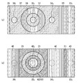
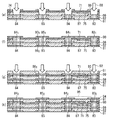
次に、図2乃至図6を参照して、本発明の実施例1のキャパシタ内蔵多層配線基板を説明する。図2及び図3は本発明の実施例1のキャパシタ内蔵多層配線基板の説明図であり、図2(a)は要部断面図であり、図2(b)は図2(a)におけるA−A′を結ぶ一点鎖線に沿った第2導体層を形成した時点の平面図であり、図3(c)は図2(a)におけるB−B′を結ぶ一点鎖線に沿った下部電極の位置の平面図であり、図3(d)は図2(a)におけるC-C′を結ぶ一点鎖線に沿った第3絶縁層を形成した直後の第3導体層の位置における平面図である。図2(a)に示すように、接地線用ビア34に接続する上部配線と一体化した第3導体層40と、電源線用ビア33に接続する下部電極25との間にキャパシタ誘電体膜21が挟まれてキャパシタを形成している。
Next, a multilayer wiring board with a built-in capacitor according to the first embodiment of the present invention will be described with reference to FIGS. 2 and 3 are explanatory diagrams of the multilayer wiring board with a built-in capacitor according to the first embodiment of the present invention, FIG. 2 (a) is a cross-sectional view of an essential part, and FIG. FIG. 3C is a plan view when the second conductor layer is formed along the alternate long and short dash line connecting −A ′, and FIG. 3C is a diagram of the lower electrode along the alternate long and short dashed line connecting BB ′ in FIG. FIG. 3D is a plan view at the position of the third conductor layer immediately after forming the third insulating layer along the alternate long and short dash line connecting CC ′ in FIG. . As shown in FIG. 2A, the capacitor dielectric film is formed between the
図2(b)に示すように、電源線用ビア33及び接地線用ビア34に接続する第2導体層36はベタパターンであり、信号線用ビア35に接続する第2導体層361は、ビア同士を接続するための接続導体パターンになっており、図においては円形にしている。図3(c)に示すように、電源線用ビア331に接続する下部電極25はベタパターンであり、下部電極25を形成する銅箔(後述する図4(a)における符号23)を利用して信号線用ビア351を取り囲む円環状の孤立導体層26を形成している。As shown in FIG. 2 (b), the second
図3(d)に示すように、電源線用ビア331及び接地線用ビア341に接続する第3導体層40はベタパターンであり、孤立導体層26に対応する位置に誘電体膜分離溝42が設けられており、キャパシタ誘電体膜21は分断されている。なお、信号線用ビア351に接続する第3導体層401は、ビア同士を接続するための接続導体パターンになっている。As shown in FIG. 3 (d), third conductor layers 40 connected to the power
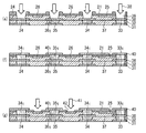
次に、図4乃至図6を参照して、本発明の実施例1のキャパシタ内蔵多層配線基板の製造工程を説明する。まず、図4(a)に示すように、厚さが2μmのBaTiO3を主成分とするキャパシタ誘電体膜21の両面に20μm厚の銅箔22,23を設けたキャパシタフィルム20を用意する。次いで、図4(b)に示すように、銅箔22を所定形状にエッチングして上部電極24を形成するとともに、銅箔23をエッチングして図3(c)に示したパターンの下部電極25及び孤立導体層26を形成する。一方、図4(c)に示すように、第1導体層31、第1絶縁層32、電源線用ビア33、接地線用ビア34、信号線用ビア35、第2導体層36,361及び第2絶縁層37を設けたベース基板30を用意する。なお、第2導体層36,361は、図2(b)に示したパターンである。Next, with reference to FIGS. 4 to 6, the manufacturing process of the multilayer wiring board with a built-in capacitor according to the first embodiment of the present invention will be described. First, as shown in FIG. 4A, a
次いで、図4(d)に示すように、ベース基板30に上部電極24、下部電極25及び孤立導体層26を形成したキャパシタ基板を下部電極25がベース基板30に対向するように押圧し、加熱して圧着して一体化する。
Next, as shown in FIG. 4D, the capacitor substrate in which the
次いで、図5(e)に示すように、上部電極24に設けた開口部からビームスポット径が100μmのCO2レーザを用いてレーザ光38を照射し、第2導体層36,361に達するビアホール39を形成する。次いで、図5(f)に示すように、ビアホール39の壁面に無電解メッキを施した後、第3導体層40,401を形成するためのパターンを設けたメッキフーレム(図示は省略)を用いてCu電解メッキを施して電源線用ビア331、接地線用ビア341、信号線用ビア351及び第3導体層40,401を形成する。なお、ここでは、図示を簡略にするために、第3導体層40,401と一体化している上部電極24は図示を省略している(以下同様である)。なお、信号線用ビア351に接続する第3導体層401は、ビア同士を接続するための接続導体パターンになっている。Then, as shown in FIG. 5 (e), the
次いで、図5(g)に示すように、再び、ビームスポット径が100μmのCO2レーザを用いて孤立導体層26に対向する位置にレーザ光41を照射して図3(d)に示す円環状の誘電体膜分離溝42を形成する。この時、レーザ照射部の下部には孤立導体層26が配置されているので、ベース基板(30)の表面がダメージを受けることがない。Next, as shown in FIG. 5 (g), again using a CO 2 laser with a beam spot diameter of 100 μm, the
以降は再び従来例と同様に、図6(h)に示すように、ビルドアップ工法を用いてエポキシ系材料を主成分とする20μm厚の絶縁フィルムにより第3絶縁層43を形成する。次いで、図6(i)に示すように、ビームスポット径が100μmのCO2レーザを用いて電源線用ビア331、接地線用ビア341及び信号線用ビア351対向する位置にレーザ光44を照射してビアホール45を形成する。Thereafter, as in the conventional example, as shown in FIG. 6H, the third insulating
次いで、図6(j)に示すように、無電解メッキを施した後、第4導体層46を形成するためのパターンを設けたメッキフーレム(図示は省略)を用いてCu電解メッキを施して電源線用ビア332、接地線用ビア342、信号線用ビア352及び第4導体層46を形成することで、キャパシタ内蔵多層配線基板の基本構成が完成する。Next, as shown in FIG. 6 (j), after electroless plating, Cu electroplating is performed using a plating frame (not shown) provided with a pattern for forming the
本発明の実施例1においては、信号線用ビア351の近傍のキャパシタ誘電体膜21の一部を円環状に除去して誘電体膜分離溝42を形成し、この誘電体膜分離溝42をキャパシタ誘電体膜21より比誘電率の小さなエポキシ樹脂で埋め込んでいる。したがって、誘電体膜分離溝42を形成しない場合に比べて、寄生キャパシタの寄生容量を低減することができる。また、本発明の実施例1においては、下部電極25を形成するための銅箔23を利用して円環状の孤立導体層26を形成しているので、誘電体膜分離溝42を形成する際のレーザ照射により、ベース基板30の表面がダメージを受けることがない。In the first embodiment of the present invention, by removing a portion of the
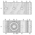
次に、図7乃至図11を参照して、本発明の実施例2のキャパシタ内蔵多層配線基板を説明する。図7及び図8は本発明の実施例2のキャパシタ内蔵多層配線基板の説明図であり、図7(a)は要部断面図であり、図7(b)は図7(a)におけるA−A′を結ぶ一点鎖線に沿った第2導体層を形成した時点の平面図であり、図7(c)は図7(a)におけるB−B′を結ぶ一点鎖線に沿った誘電体膜分離溝を形成する前の平面図であり、図7(d)は図7(a)におけるC-C′を結ぶ一点鎖線に沿った第3絶縁層を形成した直後の第3導体層の位置における平面図である。図7(a)に示すように、実施例1と同様に、接地線用ビア34に接続する上部配線と一体化した第3導体層40と、電源線用ビア33に接続する下部電極25との間にキャパシタ誘電体膜21が挟まれてキャパシタを形成している。
Next, a capacitor built-in multilayer wiring board according to a second embodiment of the present invention will be described with reference to FIGS. 7 and 8 are explanatory views of a multilayer wiring board with a built-in capacitor according to a second embodiment of the present invention, FIG. 7 (a) is a cross-sectional view of the main part, and FIG. 7 (b) is an A in FIG. FIG. 7C is a plan view when the second conductor layer is formed along the alternate long and short dash line connecting −A ′, and FIG. 7C is a dielectric film along the alternate long and short dash line connecting BB ′ in FIG. FIG. 7D is a plan view before forming the separation groove, and FIG. 7D shows the position of the third conductor layer immediately after forming the third insulating layer along the alternate long and short dash line connecting CC ′ in FIG. FIG. As shown in FIG. 7A, as in the first embodiment, the
図7(b)に示すように、電源線用ビア33及び接地線用ビア34に接続する第2導体層36はベタパターンであり、信号線用ビア35に接続する第2導体層361は、ビア同士を接続するための接続導体パターンになっている。第2導体層36を形成する際に信号線用ビア351を取り囲む円環状の孤立導体層47を形成している。As shown in FIG. 7 (b), the second
図8(c)に示すように、電源線用ビア331に接続する下部電極25はベタパターンである。図8(d)に示すように、電源線用ビア331及び接地線用ビア341に接続する第3導体層40はベタパターンであり、孤立導体層47に対応する位置に誘電体膜分離溝42が設けられており、キャパシタ誘電体膜21は分断されている。なお、信号線用ビア351に接続する第3導体層401は、ビア同士を接続するための接続導体パターンになっている。As shown in FIG. 8 (c), the
次に、図9乃至図11を参照して、本発明の実施例2のキャパシタ内蔵多層配線基板の製造工程を説明する。まず、図9(a)に示すように、厚さが2μmのBaTiO3を主成分とするキャパシタ誘電体膜21の両面に20μm厚の銅箔22,23を設けたキャパシタフィルム20を用意する。次いで、図9(b)に示すように、銅箔22を所定形状にエッチングして上部電極24を形成するとともに、銅箔23をエッチングして図8(c)に示したパターンの下部電極25を形成する。実施例2の場合には、キャパシタフィルム側に孤立導体層は形成しない。Next, with reference to FIGS. 9 to 11, the manufacturing process of the capacitor built-in multilayer wiring board according to the second embodiment of the present invention will be described. First, as shown in FIG. 9A, a
一方、図9(c)に示すように、第1導体層31、第1絶縁層32、電源線用ビア33、接地線用ビア34、信号線用ビア35、第2導体層36,361及び第2絶縁層37を設けたベース基板30を用意する。この時、第2導体層36,361を形成する際に、図7(b)に示すように、信号線用ビア35を囲む円環状の孤立導体層47を形成する。On the other hand, as shown in FIG. 9 (c), the
次いで、図9(d)に示すように、ベース基板30に上部電極24及び下部電極を形成したキャパシタ基板を下部電極25がベース基板30に対向するように押圧し、加熱して圧着して一体化する。
Next, as shown in FIG. 9D, the capacitor substrate in which the
次いで、図10(e)に示すように、上部電極24に設けた開口部からビームスポット径が100μmのCO2レーザを用いてレーザ光38を照射し、第2導体層36,361に達するビアホール39を形成する。次いで、図10(f)に示すように、ビアホール39の壁面に無電解メッキを施した後、第3導体層40,401を形成するためのパターンを設けたメッキフーレム(図示は省略)を用いてCu電解メッキを施して電源線用ビア331、接地線用ビア341、信号線用ビア351及び第3導体層40,401を形成する。なお、ここでは、図示を簡略にするために、第3導体層40,401と一体化している上部電極24は図示を省略している。Then, as shown in FIG. 10 (e), the
次いで、図10(g)に示すように、再び、ビームスポット径が100μmのCO2レーザを用いて孤立導体層47に対向する位置にレーザ光41を照射して図8(d)に示す円環状の誘電体膜分離溝42を形成する。この時、レーザ照射部の下部には孤立導体層47が配置されているので、ベース基板(30)の表面がダメージを受けることがない。Next, as shown in FIG. 10 (g), again using a CO 2 laser with a beam spot diameter of 100 μm, the
以降は再び従来例と同様に、図11(h)に示すように、ビルドアップ工法を用いてエポキシ系材料を主成分とする20μm厚の絶縁フィルムにより第3絶縁層43を形成する。次いで、図11(i)に示すように、ビームスポット径が100μmのCO2レーザを用いて電源線用ビア331、接地線用ビア341及び信号線用ビア351対向する位置にレーザ光44を照射してビアホール45を形成する。Thereafter, as in the conventional example, as shown in FIG. 11 (h), the third insulating
次いで、図11(j)に示すように、無電解メッキを施した後、第4導体層46を形成するためのパターンを設けたメッキフーレム(図示は省略)を用いてCu電解メッキを施して電源線用ビア332、接地線用ビア342、信号線用ビア352及び第4導体層46を形成することで、キャパシタ内蔵多層配線基板の基本構成が完成する。Next, as shown in FIG. 11 (j), after performing electroless plating, Cu electroplating is performed using a plating frame (not shown) provided with a pattern for forming the
本発明の実施例2においても、信号線用ビア351の近傍のキャパシタ誘電体膜21の一部を円環状に除去して誘電体膜分離溝42を形成し、この誘電体膜分離溝42をキャパシタ誘電体膜21より誘電率の小さなエポキシ樹脂で埋め込んでいる。したがって、誘電体膜分離溝42を形成しない場合に比べて、寄生キャパシタの寄生容量を低減することができる。また、第2導体層36と同時に円環状の孤立導体層47を形成しているので、誘電体膜分離溝42を形成する際のレーザ照射により、ベース基板30の表面がダメージを受けることがない。Also in the second embodiment of the present invention, by removing a portion of the
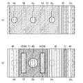
次に、図12及び図13を参照して、本発明の実施例3のキャパシタ内蔵多層配線基板を説明するが、孤立導体層47を設ける代わりに張出部48を設けた以外は上記の実施例2と製造工程は全く同様であるので、構造のみ説明する。図12及び図13は本発明の実施例3のキャパシタ内蔵多層配線基板の説明図であり、図12(a)は要部断面図であり、図12(b)図12(a)におけるA−A′を結ぶ一点鎖線に沿った第2導体層を形成した時点の平面図であり、図12(c)は図12(a)におけるB−B′を結ぶ一点鎖線に沿った誘電体膜分離溝を形成する前の下部電極位置の平面図であり、図12(d)は図12(a)におけるC-C′を結ぶ一点鎖線に沿った第3絶縁層を形成した直後の第3導体層の位置における平面図である。図12(a)に示すように、実施例2と同様に、接地線用ビア34に接続する上部配線と一体化した第3導体層40と、電源線用ビア33に接続する下部電極25との間にキャパシタ誘電体膜21が挟まれてキャパシタを形成している。
Next, a capacitor built-in multilayer wiring board according to a third embodiment of the present invention will be described with reference to FIG. 12 and FIG. 13, except that the
図12(b)に示すように、電源線用ビア33及び接地線用ビア34に接続する第2導体層36はベタパターンであり、信号線用ビア35に接続する第2導体層361は、ビア同士を接続するための接続導体パターンになっている。第2導体層36の張出部48が信号線用ビア351を取り囲んでいる。As shown in FIG. 12 (b), the second
図13(c)に示すように、電源線用ビア331に接続する下部電極25はベタパターンである。図13(d)に示すように、電源線用ビア331及び接地線用ビア341に接続する第3導体層40はベタパターンであり、張出部48が延在する位置に誘電体膜分離溝42が設けられており、キャパシタ誘電体膜21は分断されている。なお、信号線用ビア351に接続する第3導体層401は、ビア同士を接続するための接続導体パターンになっている。As shown in FIG. 13 (c), the
本発明の実施例3においては、信号線用ビア351の近傍のキャパシタ誘電体膜21の一部をリング状に除去して誘電体膜分離溝42を形成し、この誘電体膜分離溝42をキャパシタ誘電体膜21より誘電率の小さなエポキシ樹脂で埋め込んでいる。したがって、誘電体膜分離溝42を形成しない場合に比べて、寄生キャパシタの寄生容量を低減することができる。また、本発明の実施例3においては、信号線用ビア35に向かって第2導体層36の張出部48を形成しているので、誘電体膜分離溝42を形成する際のレーザ照射により、ベース基板30の表面がダメージを受けることがない。In Example 3 of the present invention, by removing a portion in the vicinity of the
次に、図14乃至図15を参照して、本発明の実施例4のキャパシタ内蔵多層配線基板を説明するが、孤立導体層を分散孤立導体層とする以外は上記の実施例1と製造工程は全く同様であるので、構造のみ説明する。図14及び図15は本発明の実施例4のキャパシタ内蔵多層配線基板の説明図であり、図14(a)は要部断面図であり、図14(b)は図14(a)におけるA−A′を結ぶ一点鎖線に沿った第2導体層を形成した時点の平面図であり、図14(c)は図14(a)におけるB−B′を結ぶ一点鎖線に沿った下部電極の位置における平面図であり、図14(d)は図14(a)におけるC-C′を結ぶ一点鎖線に沿った第3絶縁層を形成した直後の第3導体層の位置における平面図である。図14(a)に示すように、接地線用ビア34に接続する上部配線と一体化した第3導体層40と、電源線用ビア33に接続する下部電極25との間にキャパシタ誘電体膜21が挟まれてキャパシタを形成している。
Next, a multilayer wiring board with a built-in capacitor according to a fourth embodiment of the present invention will be described with reference to FIGS. 14 to 15. The manufacturing process and the above-described first embodiment except that the isolated conductor layer is a dispersed isolated conductor layer. Are exactly the same, so only the structure will be described. 14 and 15 are explanatory diagrams of a multilayer wiring board with a built-in capacitor according to a fourth embodiment of the present invention. FIG. 14 (a) is a cross-sectional view of the main part, and FIG. FIG. 14C is a plan view when the second conductor layer is formed along the alternate long and short dash line connecting −A ′, and FIG. 14C shows the lower electrode along the alternate long and short dashed line connecting BB ′ in FIG. FIG. 14D is a plan view at the position of the third conductor layer immediately after forming the third insulating layer along the alternate long and short dash line connecting CC ′ in FIG. 14A. . As shown in FIG. 14A, the capacitor dielectric film is formed between the
図14(b)に示すように、電源線用ビア33及び接地線用ビア34に接続する第2導体層36はベタパターンであり、信号線用ビア35に接続する第2導体層361は、ビア同士を接続するための接続導体パターンになっている。図15(c)に示すように、電源線用ビア331に接続する下部電極25はベタパターンであり、下部電極25を形成する銅箔(23)を利用して信号線用ビア351を取り囲むように複数の分散孤立導体層49を形成している。なお、ここでは、信号線用ビア351の接地線用ビア341に向う側に3個ずつの分散孤立導体層49を設けているが、個数は任意であり、図において、信号線用ビア351の上下も囲むように分散孤立導体層49を設けても良い。As shown in FIG. 14 (b), the second
図15(d)に示すように、電源線用ビア331及び接地線用ビア341に接続する第3導体層40はベタパターンであり、分散孤立導体層49に対応する位置に開口部50が設けられており、キャパシタ誘電体膜21は開口部50において欠落している。As shown in FIG. 15 (d), third conductor layers 40 connected to the power
本発明の実施例4においては、信号線用ビア351の近傍のキャパシタ誘電体膜21に複数の開口部50を形成し、この開口部50をキャパシタ誘電体膜21より誘電率の小さなエポキシ樹脂で埋め込んでいる。したがって、開口部50を形成しない場合に比べて、寄生キャパシタの寄生容量を低減することができる。また、本発明の実施例4においては、下部電極25を形成するための銅箔23を利用して複数の円形の分散孤立導体層49を形成しているので、開口部50を形成する際のレーザ照射により、ベース基板30の表面がダメージを受けることがない。In Example 4 of the present invention, a plurality of
次に、図16乃至図17を参照して、本発明の実施例5のキャパシタ内蔵多層配線基板を説明するが、孤立導体層を分散孤立導体層とする以外は上記の実施例2と製造工程は全く同様であるので、構造のみ説明する。図16及び図17は本発明の実施例5のキャパシタ内蔵多層配線基板の説明図であり、図16(a)は要部断面図であり、図16(b)は図16(a)におけるA−A′を結ぶ一点鎖線に沿った第2導体層を形成した時点の平面図であり、図16(c)は図16(a)におけるB−B′を結ぶ一点鎖線に沿った誘電体膜分離溝を形成する前の平面図であり、図16(d)は図16(a)におけるC-C′を結ぶ一点鎖線に沿った第3絶縁層を形成した直後の第3導体層の位置における平面図である。図16(a)に示すように、実施例5と同様に、接地線用ビア34に接続する上部配線と一体化した第3導体層40と、電源線用ビア33に接続する下部電極25との間にキャパシタ誘電体膜21が挟まれてキャパシタを形成している。
Next, a multilayer wiring board with a built-in capacitor according to a fifth embodiment of the present invention will be described with reference to FIGS. 16 to 17. The manufacturing process and the above-described second embodiment except that the isolated conductor layer is a dispersed isolated conductor layer. Are exactly the same, so only the structure will be described. 16 and 17 are explanatory views of a multilayer wiring board with a built-in capacitor according to a fifth embodiment of the present invention. FIG. 16 (a) is a cross-sectional view of an essential part, and FIG. FIG. 16C is a plan view when a second conductor layer is formed along the alternate long and short dash line connecting -A ′, and FIG. 16C is a dielectric film along the alternate long and short dash line connecting BB ′ in FIG. FIG. 16D is a plan view before forming the separation groove, and FIG. 16D shows the position of the third conductor layer immediately after forming the third insulating layer along the alternate long and short dash line connecting CC ′ in FIG. FIG. As shown in FIG. 16A, as in the fifth embodiment, the
図16(b)に示すように、電源線用ビア33及び接地線用ビア34に接続する第2導体層36はベタパターンであり、信号線用ビア35に接続する第2導体層361は、ビア同士を接続するための接続導体パターンになっている。第2導体層36,361を形成する際に信号線用ビア351を取り囲むように複数の分散孤立導体層51を形成している。なお、ここでは、信号線用ビア351の接地線用ビア341に向う側に3個ずつの分散孤立導体層51を設けているが、個数は任意であり、図において、信号線用ビア351の上下も囲むように分散孤立導体層51を設けても良い。As shown in FIG. 16 (b), the second
図17(c)に示すように、電源線用ビア331に接続する下部電極25はベタパターンである。図17(d)に示すように、電源線用ビア331及び接地線用ビア341に接続する第3導体層40はベタパターンであり、分散孤立導体層49に対応する位置に開口部52が設けられており、キャパシタ誘電体膜21は開口部52において欠落している。As shown in FIG. 17 (c), the
本発明の実施例5においては、信号線用ビア351の近傍のキャパシタ誘電体膜21に複数の開口部52を形成し、この開口部52をキャパシタ誘電体膜21より誘電率の小さなエポキシ樹脂で埋め込んで第3絶縁層43にしている。したがって、開口部52を形成しない場合に比べて、寄生キャパシタの寄生容量を低減することができる。また、本発明の実施例5においては、第2導体層36,361を形成する際に、複数の円形の分散孤立導体層51を形成しているので、開口部52を形成する際のレーザ照射により、ベース基板30の表面がダメージを受けることがない。In Example 5 of the present invention, a plurality of
次に、図18及び図19を参照して、本発明の実施例6のキャパシタ内蔵多層配線基板を説明する。実施例6は、円環状の孤立導体層57の代わりに張出部48を設け、円環状の誘電体膜分離溝の代わりに矩形状の開口部を設けた以外は上記の実施例2と製造工程は全く同様であるので構造のみ説明する。図18及び図19は本発明の実施例6のキャパシタ内蔵多層配線基板の説明図であり、図18(a)は要部断面図であり、図18(b)は図18(a)におけるA−A′を結ぶ一点鎖線に沿った第2導体層を形成した時点の平面図であり、図18(c)は図18(a)におけるB−B′を結ぶ一点鎖線に沿った誘電体膜分離溝を形成する前の平面図であり、図18(d)は図18(a)におけるC-C′を結ぶ一点鎖線に沿った第3絶縁層を形成した直後の第3導体層の位置における平面図である。図18(a)に示すように、実施例3と同様に、接地線用ビア34に接続する上部配線と一体化した第3導体層40と、電源線用ビア33に接続する下部電極25との間にキャパシタ誘電体膜21が挟まれてキャパシタを形成している。
Next, a capacitor built-in multilayer wiring board according to a sixth embodiment of the present invention will be described with reference to FIGS. Example 6 is the same as Example 2 except that an
図18(b)に示すように、電源線用ビア33及び接地線用ビア34に接続する第2導体層36はベタパターンであり、信号線用ビア35に接続する第2導体層361は、ビア同士を接続するための接続導体パターンになっている。第2導体層36の張出部48が信号線用ビア351を取り囲んでいる。As shown in FIG. 18 (b), the second
図19(c)に示すように、電源線用ビア331に接続する下部電極25はベタパターンである。図19(d)に示すように、電源線用ビア331及び接地線用ビア341に接続する第3導体層40はベタパターンであり、張出部48が延在する位置に複数の開口部53を形成している。なお、ここでは、信号線用ビア351の接地線用ビア341に向う側に3個ずつの開口部53を設けているが、個数は任意であり、図において、信号線用ビア351の上下も囲むように開口部53を設けても良い。As shown in FIG. 19 (c), the
本発明の実施例6においては、信号線用ビア351の近傍のキャパシタ誘電体膜21に複数の開口部53を形成し、この開口部53をキャパシタ誘電体膜21より誘電率の小さなエポキシ樹脂で埋め込んで第4絶縁層46にしている。したがって、開口部53を形成しない場合に比べて、寄生キャパシタの寄生容量を低減することができる。また、本発明の実施例6においては、信号線用ビア35に向かって第2導体層36の張出部48を形成しているので、開口部53を形成する際のレーザ照射により、ベース基板30の表面がダメージを受けることがない。In Example 6 of the present invention, a plurality of
次に、図20乃至図21を参照して、本発明の実施例7のキャパシタ内蔵多層配線基板を説明するが、円環状の孤立導体層を矩形状の孤立導体層とする以外は上記の実施例1と製造工程は全く同様であるので、構造のみ説明する。図20及び図21は本発明の実施例7のキャパシタ内蔵多層配線基板の説明図であり、図20(a)は要部断面図であり、図20(b)は図20(a)におけるA−A′を結ぶ一点鎖線に沿った第2導体層を形成した時点の平面図であり、図20(c)は図20(a)におけるB−B′を結ぶ一点鎖線に沿った下部電極の位置における平面図であり、図20(d)は図20(a)におけるC-C′を結ぶ一点鎖線に沿った第3絶縁層を形成した直後の第3導体層の位置における平面図である。図21(a)に示すように、接地線用ビア34に接続する上部配線と一体化した第3導体層40と、電源線用ビア33に接続する下部電極25との間にキャパシタ誘電体膜21が挟まれてキャパシタを形成している。
Next, a multilayer wiring board with a built-in capacitor according to a seventh embodiment of the present invention will be described with reference to FIGS. 20 to 21. The above implementation is performed except that the annular isolated conductor layer is a rectangular isolated conductor layer. Since the manufacturing process is exactly the same as Example 1, only the structure will be described. 20 and 21 are explanatory views of a multilayer wiring board with a built-in capacitor according to a seventh embodiment of the present invention. FIG. 20 (a) is a cross-sectional view of the main part, and FIG. FIG. 20C is a plan view when the second conductor layer is formed along the alternate long and short dash line connecting −A ′, and FIG. 20C is a diagram of the lower electrode along the alternate long and short dash line connecting BB ′ in FIG. FIG. 20D is a plan view at the position of the third conductor layer immediately after forming the third insulating layer along the alternate long and short dash line connecting CC ′ in FIG. . As shown in FIG. 21A, a capacitor dielectric film is formed between the
図20(b)に示すように、電源線用ビア33及び接地線用ビア34に接続する第2導体層36はベタパターンであり、信号線用ビア35に接続する第2導体層361は、ビア同士を接続するための接続導体パターンになっている。図21(c)に示すように、電源線用ビア331に接続する下部電極25はベタパターンであり、下部電極25を形成する銅箔(23)を利用して信号線用ビア351の両側に長方形状の孤立導体層55を形成している。なお、ここでは、信号線用ビア351の接地線用ビア341に向う側に一対の孤立導体層55を設けているが、図において、信号線用ビア351の上下にも孤立導体層55を設けても良い。As shown in FIG. 20 (b), the second
図21(d)に示すように、電源線用ビア331及び接地線用ビア341に接続する第3導体層40はベタパターンであり、孤立導体層55に対応する位置に開口部56が設けられており、キャパシタ誘電体膜21は開口部56において欠落している。As shown in FIG. 21 (d), third conductor layers 40 connected to the power
本発明の実施例7においては、信号線用ビア351の近傍のキャパシタ誘電体膜21に孤立導体層55に対応する一対の開口部56を形成し、この開口部56をキャパシタ誘電体膜21より誘電率の小さなエポキシ樹脂で埋め込んで第4絶縁層46を形成している。したがって、開口部56を形成しない場合に比べて、寄生キャパシタの寄生容量を低減することができる。また、本発明の実施例7においては、下部電極25を形成するための銅箔23を利用して一対の孤立導体層55を形成しているので、開口部56を形成する際のレーザ照射により、ベース基板30の表面がダメージを受けることがない。In Example 7 of the present invention forms a pair of
次に、図22乃至図23を参照して、本発明の実施例8のキャパシタ内蔵多層配線基板を説明するが円環状の孤立導体層を矩形の孤立導体層とする以外は上記の実施例2と製造工程は全く同様であるので、構造のみ説明する。図22及び図23は本発明の実施例8のキャパシタ内蔵多層配線基板の説明図であり、図22(a)は要部断面図であり、図22(b)は図22(a)におけるA−A′を結ぶ一点鎖線に沿った第2導体層を形成した時点の平面図であり、図22(c)は図22(a)におけるB−B′を結ぶ一点鎖線に沿った誘電体膜分離溝を形成する前の平面図であり、図20(d)は図20(a)におけるC-C′を結ぶ一点鎖線に沿った第3絶縁層を形成した直後の第3導体層の位置における平面図である。図22(a)に示すように、実施例8と同様に、接地線用ビア34に接続する上部配線と一体化した第3導体層40と、電源線用ビア33に接続する下部電極25との間にキャパシタ誘電体膜21が挟まれてキャパシタを形成している。
Next, a multilayer wiring board with a built-in capacitor according to an eighth embodiment of the present invention will be described with reference to FIGS. 22 to 23, but the second embodiment described above except that the annular isolated conductor layer is a rectangular isolated conductor layer. Since the manufacturing process is exactly the same, only the structure will be described. 22 and 23 are explanatory views of a multilayer wiring board with a built-in capacitor according to an eighth embodiment of the present invention, FIG. 22 (a) is a cross-sectional view of the main part, and FIG. 22 (b) is an A in FIG. FIG. 22C is a plan view when the second conductor layer is formed along the alternate long and short dash line connecting −A ′, and FIG. 22C is a dielectric film along the alternate long and short dash line connecting BB ′ in FIG. FIG. 20D is a plan view before forming the separation groove, and FIG. 20D is the position of the third conductor layer immediately after forming the third insulating layer along the alternate long and short dash line connecting CC ′ in FIG. FIG. As shown in FIG. 22A, as in the eighth embodiment, the
図22(b)に示すように、電源線用ビア33及び接地線用ビア34に接続する第2導体層36はベタパターンであり、信号線用ビア35に接続する第2導体層361は、ビア同士を接続するための接続導体パターンになっている。第2導体層36,361を形成する際に信号線用ビア351の両側に長方形状の孤立導体層57を形成している。なお、ここでは、信号線用ビア351の接地線用ビア341に向う側に1対の孤立導体層57を設けているが、図において、信号線用ビア351の上下にも孤立導体層57を設けても良い。As shown in FIG. 22 (b), the second
図23(c)に示すように、電源線用ビア331に接続する下部電極25はベタパターンである。図23(d)に示すように、電源線用ビア331及び接地線用ビア341に接続する第3導体層40はベタパターンであり、一対の孤立導体層57に対応する位置に開口部58が設けられており、キャパシタ誘電体膜21は開口部58において欠落している。As shown in FIG. 23 (c), the
本発明の実施例8においては、信号線用ビア351の近傍のキャパシタ誘電体膜21に一対の開口部58を形成し、この開口部58をキャパシタ誘電体膜21より誘電率の小さなエポキシ樹脂で埋め込んで第4絶縁層46にしている。したがって、開口部58を形成しない場合に比べて、寄生キャパシタの寄生容量を低減することができる。また、本発明の実施例8においては、第2導体層36,361を形成する際に、一対の孤立導体層57を形成しているので、開口部58を形成する際のレーザ照射により、ベース基板30の表面がダメージを受けることがない。In Example 8 of the present invention, to form a pair of
次に、図24及び図25を参照して、本発明の実施例9のキャパシタ内蔵多層配線基板を説明する。実施例9は、円環状の孤立導体層57の代わりに張出部48を設け、円環状の誘電体膜分離溝の代わりに矩形状の開口部を設けた以外は上記の実施例2と製造工程は全く同様であるので構造のみ説明する。図24及び図25は本発明の実施例9のキャパシタ内蔵多層配線基板の説明図であり、図24(a)は要部断面図であり、図24(b)は図24(a)におけるA−A′を結ぶ一点鎖線に沿った第2導体層を形成した時点の平面図であり、図24(c)は図24(a)におけるB−B′を結ぶ一点鎖線に沿った誘電体膜分離溝を形成する前の平面図であり、図24(d)は図24(a)におけるC-C′を結ぶ一点鎖線に沿った第3絶縁層を形成した直後の第3導体層の位置における平面図である。図24(a)に示すように、実施例3と同様に、接地線用ビア34に接続する上部配線と一体化した第3導体層40と、電源線用ビア33に接続する下部電極25との間にキャパシタ誘電体膜21が挟まれてキャパシタを形成している。
Next, with reference to FIG. 24 and FIG. 25, the multilayer wiring board with a built-in capacitor according to the ninth embodiment of the present invention will be described. Example 9 is the same as Example 2 except that an
図24(b)に示すように、電源線用ビア33及び接地線用ビア34に接続する第2導体層36はベタパターンであり、信号線用ビア35に接続する第2導体層361は、ビア同士を接続するための接続導体パターンになっている。第2導体層36の張出部48が信号線用ビア351を取り囲んでいる。As shown in FIG. 24 (b), the second
図25(c)に示すように、電源線用ビア331に接続する下部電極25はベタパターンである。図25(d)に示すように、電源線用ビア331及び接地線用ビア341に接続する第3導体層40はベタパターンであり、張出部48が延在する位置に一対の長方形状の開口部59を形成している。なお、ここでは、信号線用ビア351の接地線用ビア341に向う側に1対の開口部59を設けているが図において、信号線用ビア351の上下にも開口部59を設けても良い。As shown in FIG. 25 (c), the
本発明の実施例9においては、信号線用ビア351の近傍のキャパシタ誘電体膜21に複数の開口部59を形成し、この開口部59をキャパシタ誘電体膜21より誘電率の小さなエポキシ樹脂で埋め込んで第4絶縁層46にしている。したがって、開口部59を形成しない場合に比べて、寄生キャパシタの寄生容量を低減することができる。また、本発明の実施例9においては、信号線用ビア35に向かって第2導体層36の張出部48を形成しているので、開口部59を形成する際のレーザ照射により、ベース基板30の表面がダメージを受けることがない。In Example 9 of the present invention, a plurality of
1 第1の信号線用ビア
2 第1の接地線用ビア
3 第1の電源線用ビア
4 第1導体層群
5 第1絶縁層
6 第2導体層
7 第2絶縁層
8 第2の信号線用ビア
9 第2の接地線用ビア
10 第2の電源線用ビア
11 第3導体層群
12 貫通開口部
13 導体パターン
14 第3絶縁層
15 キャパシタ
21,71 キャパシタ誘電体膜
22,23,72,73 銅箔
24,74 上部電極
25,75 下部電極
26 孤立導体層
30,80 ベース基板
31,81 第1導体層
32,82 第1絶縁層
33,331,332,83,831,832 電源線用ビア
34,341,342,84,841,842 接地線用ビア
35,351,352,85,851,852 信号線用ビア
36,361,86 第2導体層
37,87 第2絶縁層
38,88 レーザ光
39,89 ビアホール
40,401,90,901 第3導体層
41 レーザ光
42 誘電体膜分離溝
43,91 第3絶縁層
44,92 レーザ光
45,93 ビアホール
46,94 第4導体層
47 孤立導体層
48 張出部
49,51,55 分散孤立導体層
50,52,53,56,58,59 開口部
57 孤立導体層
95 キャパシタDESCRIPTION OF SYMBOLS 1 1st signal line via 2 1st grounding line via 3 1st power supply line via 4 1st conductor layer group 5 1st insulating layer 6 2nd conductor layer 7 2nd insulating layer 8 2nd signal Line via 9 Second ground line via 10 Second power line via 11 Third conductor layer group 12 Through opening 13 Conductor pattern 14 Third insulating layer 15 Capacitors 21, 71 Capacitor dielectric films 22, 23, 72, 73 Copper foils 24, 74 Upper electrode 25, 75 Lower electrode 26 Isolated conductor layer 30, 80 Base substrate 31, 81 First conductor layer 32, 82 First insulating layer 33, 33 1 , 33 2 , 83, 83 1 83 2 Power line vias 34, 34 1 , 34 2 , 84, 84 1 , 84 2 Ground line vias 35, 35 1 , 35 2 , 85, 85 1 , 85 2 Signal line vias 36, 36 1 , 86 Second conductor layers 37 and 87 Second insulating layers 38 and 88 The light 39, 89 Via holes 40, 40 1 , 90, 90 1 Third conductor layer 41 Laser light 42 Dielectric film separation grooves 43, 91 Third insulating layers 44, 92 Laser light 45, 93 Via holes 46, 94 Fourth conductor Layer 47 Isolated conductor layer 48 Overhang 49, 51, 55 Dispersed isolated conductor layer 50, 52, 53, 56, 58, 59 Opening 57 Isolated conductor layer 95 Capacitor
Claims (14)
前記信号線用積層ビア、前記接地線用積層ビア及び前記電源線用積層ビアに個別に電気的に接続する第1配線層準位に形成された複数の第1導体層群と、
少なくとも前記電源線用積層ビアに個別に電気的に接続する第2配線層準位に形成された第2導体層と、
前記信号線用積層ビア、前記接地線用積層ビア及び前記電源線用積層ビアに個別に電気的に接続する第3配線層準位に形成された複数の第3導体層群と、
前記第1配線層準位と前記第2配線層準位との間に形成された第1絶縁層と、
前記第2配線層準位と前記第3配線層準位との間に形成された第2絶縁層と
を有し、
前記第2絶縁層は前記信号線用積層ビアの近傍において第3絶縁層で埋め込まれた貫通開口部を有し、
前記第2絶縁層の比誘電率が、前記第1絶縁層及び前記第3絶縁層の比誘電率より高く、
前記貫通開口部が導体パターンに達しているキャパシタ内蔵多層配線基板。Signal line laminated vias, ground line laminated vias and power line laminated vias;
A plurality of first conductor layer groups formed at first wiring layer levels that are individually electrically connected to the signal line stacked vias, the ground line stacked vias, and the power supply line stacked vias;
A second conductor layer formed in at least a second wiring layer level that is electrically connected to at least the power line laminated via;
A plurality of third conductor layer groups formed at third wiring layer levels that are individually electrically connected to the signal line laminated via, the ground line laminated via, and the power line laminated via;
A first insulating layer formed between the first wiring layer level and the second wiring layer level;
A second insulating layer formed between the second wiring layer level and the third wiring layer level;
The second insulating layer has a through opening embedded with a third insulating layer in the vicinity of the signal line laminated via,
A relative dielectric constant of the second insulating layer is higher than a relative dielectric constant of the first insulating layer and the third insulating layer;
A multilayer wiring board with a built-in capacitor in which the through opening reaches a conductor pattern.
前記第1導体層群に接続する第2の電源線用ビア、第2の接地線用ビア及び第2の信号線用ビアと、前記第2の電源線用ビア、第2の接地線用ビア及び第2の信号線用ビアに独立して電気的に接続し、前記第3導体パターンと一体化した第3配線層準位に形成された第3導体層群を形成する工程と、
前記第2の信号線用ビアの近傍において前記第2絶縁層に貫通開口部を形成する工程と、
前記貫通開口部を前記第2絶縁層の比誘電率より小さい第3絶縁層で埋め込む工程と
を有し、
前記第2の信号線用ビアの近傍において前記第2絶縁層に貫通開口部を形成する工程において、前記第2絶縁層の下部に設けた導体パターンに達するように前記貫通開口部を形成するキャパシタ内蔵多層配線基板の製造方法。At least a first power line via, a first ground line via, and a first signal line via, the first power line via, the first ground line via, and the first signal line. A first conductor layer group formed at a first wiring layer level that is electrically connected independently to the via, and a base substrate including a first insulating layer provided on the first conductor layer group; The second insulating layer is provided with a second conductor pattern on one surface and a capacitor substrate on which the third conductor pattern is provided on the other surface. Forming a two-conductor pattern as a second conductor layer;
A second power line via, a second ground line via, a second signal line via, a second power line via, and a second ground line via connected to the first conductor layer group; And a step of forming a third conductor layer group formed in a third wiring layer level integrally connected to the second signal line via and electrically connected to the third conductor pattern;
Forming a through opening in the second insulating layer in the vicinity of the second signal line via;
Filling the through-opening with a third insulating layer having a dielectric constant smaller than that of the second insulating layer,
Capacitor for forming the through-opening so as to reach a conductor pattern provided under the second insulating layer in the step of forming the through-opening in the second insulating layer in the vicinity of the second signal line via Manufacturing method of built-in multilayer wiring board.
Applications Claiming Priority (1)
| Application Number | Priority Date | Filing Date | Title |
|---|---|---|---|
| PCT/JP2016/053155 WO2017134761A1 (en) | 2016-02-03 | 2016-02-03 | Capacitor-incorporated multilayer wiring board and method for manufacturing same |
Publications (2)
| Publication Number | Publication Date |
|---|---|
| JPWO2017134761A1 JPWO2017134761A1 (en) | 2018-11-22 |
| JP6614246B2 true JP6614246B2 (en) | 2019-12-04 |
Family
ID=59500201
Family Applications (1)
| Application Number | Title | Priority Date | Filing Date |
|---|---|---|---|
| JP2017565012A Expired - Fee Related JP6614246B2 (en) | 2016-02-03 | 2016-02-03 | Capacitor built-in multilayer wiring board and manufacturing method thereof |
Country Status (3)
| Country | Link |
|---|---|
| US (2) | US10362677B2 (en) |
| JP (1) | JP6614246B2 (en) |
| WO (1) | WO2017134761A1 (en) |
Families Citing this family (9)
| Publication number | Priority date | Publication date | Assignee | Title |
|---|---|---|---|---|
| KR102502866B1 (en) * | 2017-10-18 | 2023-02-23 | 엘지이노텍 주식회사 | Printed circuit board and package substrate comprising same |
| US10923443B2 (en) * | 2019-03-29 | 2021-02-16 | Intel Corporation | Electronic device package including a capacitor |
| US11950357B2 (en) | 2019-11-27 | 2024-04-02 | Qing Ding Precision Electronics (Huaian) Co., Ltd | Circuit board for transmitting high-frequency signal and method for manufacturing the same |
| US11205696B2 (en) | 2019-12-24 | 2021-12-21 | Skyworks Solutions, Inc. | High dielectric constant material at locations of high fields |
| JP7427966B2 (en) * | 2020-01-16 | 2024-02-06 | Tdk株式会社 | electronic components |
| US11302645B2 (en) * | 2020-06-30 | 2022-04-12 | Western Digital Technologies, Inc. | Printed circuit board compensation structure for high bandwidth and high die-count memory stacks |
| CN113066799B (en) * | 2021-03-16 | 2022-08-19 | 泉芯集成电路制造(济南)有限公司 | Semiconductor device and method for manufacturing the same |
| US11626366B2 (en) | 2021-06-22 | 2023-04-11 | Silicon Laboratories Inc. | Shielding using layers with staggered trenches |
| US20240088015A1 (en) * | 2022-09-08 | 2024-03-14 | Samsung Electronics Co., Ltd. | Integrated circuit devices including via capacitors |
Family Cites Families (19)
| Publication number | Priority date | Publication date | Assignee | Title |
|---|---|---|---|---|
| JPS58158996A (en) | 1982-03-16 | 1983-09-21 | 日本電気株式会社 | Multilayer printed circuit board |
| JPH0632384B2 (en) * | 1987-12-22 | 1994-04-27 | 株式会社住友金属セラミックス | Method for manufacturing laminated ceramic substrate |
| JP3732927B2 (en) * | 1997-07-31 | 2006-01-11 | 京セラ株式会社 | Multilayer wiring board |
| US6072690A (en) * | 1998-01-15 | 2000-06-06 | International Business Machines Corporation | High k dielectric capacitor with low k sheathed signal vias |
| JPH11204946A (en) * | 1998-01-19 | 1999-07-30 | Nippon Avionics Co Ltd | Components-contg. ceramic circuit board |
| JP2001267751A (en) | 2000-03-22 | 2001-09-28 | Matsushita Electric Ind Co Ltd | Capacitor-incorporating substrate and its manufacturing method |
| US6847527B2 (en) * | 2001-08-24 | 2005-01-25 | 3M Innovative Properties Company | Interconnect module with reduced power distribution impedance |
| US7164197B2 (en) * | 2003-06-19 | 2007-01-16 | 3M Innovative Properties Company | Dielectric composite material |
| JP4377617B2 (en) * | 2003-06-20 | 2009-12-02 | 日本特殊陶業株式会社 | Capacitor, semiconductor element with capacitor, wiring board with capacitor, and electronic unit including semiconductor element, capacitor, and wiring board |
| US7566960B1 (en) * | 2003-10-31 | 2009-07-28 | Xilinx, Inc. | Interposing structure |
| US6875921B1 (en) * | 2003-10-31 | 2005-04-05 | Xilinx, Inc. | Capacitive interposer |
| US7233061B1 (en) * | 2003-10-31 | 2007-06-19 | Xilinx, Inc | Interposer for impedance matching |
| JP2006261658A (en) | 2005-02-16 | 2006-09-28 | Ngk Spark Plug Co Ltd | Wiring board and manufacturing method therefor |
| EP1909546A4 (en) * | 2005-06-13 | 2009-11-11 | Ibiden Co Ltd | Printed wiring board |
| US20070004844A1 (en) * | 2005-06-30 | 2007-01-04 | Clough Robert S | Dielectric material |
| JP4830539B2 (en) | 2006-02-28 | 2011-12-07 | 日本電気株式会社 | Multilayer printed circuit board |
| US7336501B2 (en) * | 2006-06-26 | 2008-02-26 | Ibiden Co., Ltd. | Wiring board with built-in capacitor |
| JP2010087499A (en) * | 2008-09-30 | 2010-04-15 | Ibiden Co Ltd | Method of manufacturing capacitor device |
| JP2015053350A (en) * | 2013-09-06 | 2015-03-19 | パナソニック株式会社 | Board having built-in capacitor, method of manufacturing the same and semiconductor device using the same |
-
2016
- 2016-02-03 JP JP2017565012A patent/JP6614246B2/en not_active Expired - Fee Related
- 2016-02-03 WO PCT/JP2016/053155 patent/WO2017134761A1/en active Application Filing
-
2018
- 2018-07-24 US US16/043,603 patent/US10362677B2/en not_active Expired - Fee Related
-
2019
- 2019-06-07 US US16/434,218 patent/US10701808B2/en not_active Expired - Fee Related
Also Published As
| Publication number | Publication date |
|---|---|
| JPWO2017134761A1 (en) | 2018-11-22 |
| US20180332707A1 (en) | 2018-11-15 |
| US20190289718A1 (en) | 2019-09-19 |
| WO2017134761A1 (en) | 2017-08-10 |
| US10701808B2 (en) | 2020-06-30 |
| US10362677B2 (en) | 2019-07-23 |
Similar Documents
| Publication | Publication Date | Title |
|---|---|---|
| JP6614246B2 (en) | Capacitor built-in multilayer wiring board and manufacturing method thereof | |
| US20180261578A1 (en) | Package structure and method of manufacturing the same | |
| US7338892B2 (en) | Circuit carrier and manufacturing process thereof | |
| TW201422093A (en) | Hybrid lamination substrate, manufacturing method thereof and package substrate | |
| KR101883046B1 (en) | Coil Electronic Component | |
| JP7294584B2 (en) | Inductor and its manufacturing method | |
| KR20160066311A (en) | semi-conductor package and manufacturing method thereof | |
| WO2014162478A1 (en) | Component-embedded substrate and manufacturing method for same | |
| JP2008270532A (en) | Substrate with built-in inductor and manufacturing method thereof | |
| WO2011102134A1 (en) | Component-embedded substrate | |
| US7393720B2 (en) | Method for fabricating electrical interconnect structure | |
| KR102281452B1 (en) | A printed circuit board comprising embeded electronic component within and a method for manufacturing | |
| JP5842859B2 (en) | Multilayer wiring board and module having the same | |
| TWI558285B (en) | Flexible circuit board, method for making the same, and electronic device having the same | |
| TWI678952B (en) | Circuit board structure and manufacturing method thereof | |
| KR20160004157A (en) | Chip embedded substrate and method of manufacturing the same | |
| US20050157447A1 (en) | Structure of multi-electrode capacitor and method for manufacturing process of the same | |
| JP2009004457A (en) | Multi-layer substrate having capacitor therein | |
| TWI615075B (en) | Flexible circuit board and manufacturing method for same | |
| TWI580331B (en) | Multilayer circuit board with cavity and manufacturing method thereof | |
| JP6105517B2 (en) | Wiring board | |
| US6969912B2 (en) | Embedded microelectronic capacitor incorporating ground shielding layers and method for fabrication | |
| KR100653247B1 (en) | Printed circuit board having embedded electric components and fabricating method therefore | |
| JP2010171348A (en) | Wiring board and stacked ceramic capacitor | |
| JPH0669662A (en) | Multilayered printed wiring board |
Legal Events
| Date | Code | Title | Description |
|---|---|---|---|
| A621 | Written request for application examination |
Free format text: JAPANESE INTERMEDIATE CODE: A621 Effective date: 20180802 |
|
| TRDD | Decision of grant or rejection written | ||
| A01 | Written decision to grant a patent or to grant a registration (utility model) |
Free format text: JAPANESE INTERMEDIATE CODE: A01 Effective date: 20191008 |
|
| A61 | First payment of annual fees (during grant procedure) |
Free format text: JAPANESE INTERMEDIATE CODE: A61 Effective date: 20191021 |
|
| R150 | Certificate of patent or registration of utility model |
Ref document number: 6614246 Country of ref document: JP Free format text: JAPANESE INTERMEDIATE CODE: R150 |
|
| LAPS | Cancellation because of no payment of annual fees |