KR20150119179A - Led module with hermetic seal of wavelength conversion material - Google Patents
Led module with hermetic seal of wavelength conversion material Download PDFInfo
- Publication number
- KR20150119179A KR20150119179A KR1020157024839A KR20157024839A KR20150119179A KR 20150119179 A KR20150119179 A KR 20150119179A KR 1020157024839 A KR1020157024839 A KR 1020157024839A KR 20157024839 A KR20157024839 A KR 20157024839A KR 20150119179 A KR20150119179 A KR 20150119179A
- Authority
- KR
- South Korea
- Prior art keywords
- substrate
- top plate
- cavity
- cavities
- wavelength conversion
- Prior art date
Links
Images


Classifications
-
- H—ELECTRICITY
- H01—ELECTRIC ELEMENTS
- H01L—SEMICONDUCTOR DEVICES NOT COVERED BY CLASS H10
- H01L25/00—Assemblies consisting of a plurality of individual semiconductor or other solid state devices ; Multistep manufacturing processes thereof
- H01L25/03—Assemblies consisting of a plurality of individual semiconductor or other solid state devices ; Multistep manufacturing processes thereof all the devices being of a type provided for in the same subgroup of groups H01L27/00 - H01L33/00, or in a single subclass of H10K, H10N, e.g. assemblies of rectifier diodes
- H01L25/04—Assemblies consisting of a plurality of individual semiconductor or other solid state devices ; Multistep manufacturing processes thereof all the devices being of a type provided for in the same subgroup of groups H01L27/00 - H01L33/00, or in a single subclass of H10K, H10N, e.g. assemblies of rectifier diodes the devices not having separate containers
- H01L25/075—Assemblies consisting of a plurality of individual semiconductor or other solid state devices ; Multistep manufacturing processes thereof all the devices being of a type provided for in the same subgroup of groups H01L27/00 - H01L33/00, or in a single subclass of H10K, H10N, e.g. assemblies of rectifier diodes the devices not having separate containers the devices being of a type provided for in group H01L33/00
- H01L25/0753—Assemblies consisting of a plurality of individual semiconductor or other solid state devices ; Multistep manufacturing processes thereof all the devices being of a type provided for in the same subgroup of groups H01L27/00 - H01L33/00, or in a single subclass of H10K, H10N, e.g. assemblies of rectifier diodes the devices not having separate containers the devices being of a type provided for in group H01L33/00 the devices being arranged next to each other
-
- H—ELECTRICITY
- H01—ELECTRIC ELEMENTS
- H01L—SEMICONDUCTOR DEVICES NOT COVERED BY CLASS H10
- H01L33/00—Semiconductor devices with at least one potential-jump barrier or surface barrier specially adapted for light emission; Processes or apparatus specially adapted for the manufacture or treatment thereof or of parts thereof; Details thereof
- H01L33/48—Semiconductor devices with at least one potential-jump barrier or surface barrier specially adapted for light emission; Processes or apparatus specially adapted for the manufacture or treatment thereof or of parts thereof; Details thereof characterised by the semiconductor body packages
- H01L33/483—Containers
- H01L33/486—Containers adapted for surface mounting
-
- H—ELECTRICITY
- H01—ELECTRIC ELEMENTS
- H01L—SEMICONDUCTOR DEVICES NOT COVERED BY CLASS H10
- H01L33/00—Semiconductor devices with at least one potential-jump barrier or surface barrier specially adapted for light emission; Processes or apparatus specially adapted for the manufacture or treatment thereof or of parts thereof; Details thereof
- H01L33/48—Semiconductor devices with at least one potential-jump barrier or surface barrier specially adapted for light emission; Processes or apparatus specially adapted for the manufacture or treatment thereof or of parts thereof; Details thereof characterised by the semiconductor body packages
- H01L33/50—Wavelength conversion elements
- H01L33/501—Wavelength conversion elements characterised by the materials, e.g. binder
-
- H—ELECTRICITY
- H01—ELECTRIC ELEMENTS
- H01L—SEMICONDUCTOR DEVICES NOT COVERED BY CLASS H10
- H01L33/00—Semiconductor devices with at least one potential-jump barrier or surface barrier specially adapted for light emission; Processes or apparatus specially adapted for the manufacture or treatment thereof or of parts thereof; Details thereof
- H01L33/48—Semiconductor devices with at least one potential-jump barrier or surface barrier specially adapted for light emission; Processes or apparatus specially adapted for the manufacture or treatment thereof or of parts thereof; Details thereof characterised by the semiconductor body packages
- H01L33/50—Wavelength conversion elements
- H01L33/505—Wavelength conversion elements characterised by the shape, e.g. plate or foil
-
- H—ELECTRICITY
- H01—ELECTRIC ELEMENTS
- H01L—SEMICONDUCTOR DEVICES NOT COVERED BY CLASS H10
- H01L33/00—Semiconductor devices with at least one potential-jump barrier or surface barrier specially adapted for light emission; Processes or apparatus specially adapted for the manufacture or treatment thereof or of parts thereof; Details thereof
- H01L33/48—Semiconductor devices with at least one potential-jump barrier or surface barrier specially adapted for light emission; Processes or apparatus specially adapted for the manufacture or treatment thereof or of parts thereof; Details thereof characterised by the semiconductor body packages
- H01L33/52—Encapsulations
- H01L33/54—Encapsulations having a particular shape
-
- H—ELECTRICITY
- H01—ELECTRIC ELEMENTS
- H01L—SEMICONDUCTOR DEVICES NOT COVERED BY CLASS H10
- H01L33/00—Semiconductor devices with at least one potential-jump barrier or surface barrier specially adapted for light emission; Processes or apparatus specially adapted for the manufacture or treatment thereof or of parts thereof; Details thereof
- H01L33/48—Semiconductor devices with at least one potential-jump barrier or surface barrier specially adapted for light emission; Processes or apparatus specially adapted for the manufacture or treatment thereof or of parts thereof; Details thereof characterised by the semiconductor body packages
- H01L33/62—Arrangements for conducting electric current to or from the semiconductor body, e.g. lead-frames, wire-bonds or solder balls
-
- H—ELECTRICITY
- H01—ELECTRIC ELEMENTS
- H01L—SEMICONDUCTOR DEVICES NOT COVERED BY CLASS H10
- H01L33/00—Semiconductor devices with at least one potential-jump barrier or surface barrier specially adapted for light emission; Processes or apparatus specially adapted for the manufacture or treatment thereof or of parts thereof; Details thereof
- H01L33/48—Semiconductor devices with at least one potential-jump barrier or surface barrier specially adapted for light emission; Processes or apparatus specially adapted for the manufacture or treatment thereof or of parts thereof; Details thereof characterised by the semiconductor body packages
- H01L33/64—Heat extraction or cooling elements
- H01L33/642—Heat extraction or cooling elements characterized by the shape
-
- H—ELECTRICITY
- H01—ELECTRIC ELEMENTS
- H01L—SEMICONDUCTOR DEVICES NOT COVERED BY CLASS H10
- H01L2924/00—Indexing scheme for arrangements or methods for connecting or disconnecting semiconductor or solid-state bodies as covered by H01L24/00
- H01L2924/0001—Technical content checked by a classifier
- H01L2924/0002—Not covered by any one of groups H01L24/00, H01L24/00 and H01L2224/00
-
- H—ELECTRICITY
- H01—ELECTRIC ELEMENTS
- H01L—SEMICONDUCTOR DEVICES NOT COVERED BY CLASS H10
- H01L2924/00—Indexing scheme for arrangements or methods for connecting or disconnecting semiconductor or solid-state bodies as covered by H01L24/00
- H01L2924/10—Details of semiconductor or other solid state devices to be connected
- H01L2924/11—Device type
- H01L2924/12—Passive devices, e.g. 2 terminal devices
- H01L2924/1204—Optical Diode
- H01L2924/12041—LED
-
- H—ELECTRICITY
- H01—ELECTRIC ELEMENTS
- H01L—SEMICONDUCTOR DEVICES NOT COVERED BY CLASS H10
- H01L2933/00—Details relating to devices covered by the group H01L33/00 but not provided for in its subgroups
- H01L2933/0008—Processes
- H01L2933/0033—Processes relating to semiconductor body packages
- H01L2933/0041—Processes relating to semiconductor body packages relating to wavelength conversion elements
-
- H—ELECTRICITY
- H01—ELECTRIC ELEMENTS
- H01L—SEMICONDUCTOR DEVICES NOT COVERED BY CLASS H10
- H01L33/00—Semiconductor devices with at least one potential-jump barrier or surface barrier specially adapted for light emission; Processes or apparatus specially adapted for the manufacture or treatment thereof or of parts thereof; Details thereof
- H01L33/48—Semiconductor devices with at least one potential-jump barrier or surface barrier specially adapted for light emission; Processes or apparatus specially adapted for the manufacture or treatment thereof or of parts thereof; Details thereof characterised by the semiconductor body packages
- H01L33/58—Optical field-shaping elements
Landscapes
- Engineering & Computer Science (AREA)
- Microelectronics & Electronic Packaging (AREA)
- Power Engineering (AREA)
- Computer Hardware Design (AREA)
- Manufacturing & Machinery (AREA)
- Physics & Mathematics (AREA)
- Condensed Matter Physics & Semiconductors (AREA)
- General Physics & Mathematics (AREA)
- Led Device Packages (AREA)
Abstract
LED 모듈은 높은 열 전도율을 가지는 기판 및 기판 상에 마운팅된 적어도 하나의 LED 다이를 포함한다. 바인더 내의 인광체 또는 양자 점들과 같은 파장 변환 재료는 매우 낮은 열 전도율을 가지고, 비교적 큰 부피와 낮은 농도를 가지도록 LED 다이 상에 형성되고, 이에 의하여 인광체 또는 양자 점들은 열을 LED 다이로부터 적게 전도한다. 높은 열 전도율을 가지는 투명 상부 플레이트는 파장 변환 재료 위에 위치되고, 기밀 밀봉이 상부 플레이트와 파장 변환 재료를 둘러싸는 기판 사이에서 형성된다. LED 다이는 기판 또는 상부 플레이트의 캐비티 내에 위치된다. 이 방식에서, 파장 변환 재료의 온도는 LED 다이의 온도 미만으로 잘 유지된다. 밀봉은 웨이퍼 레벨 프로세스에서 수행된다.The LED module includes a substrate having a high thermal conductivity and at least one LED die mounted on the substrate. Wavelength conversion materials, such as phosphors or quantum dots in the binder, are formed on the LED die to have a relatively low thermal conductivity and a relatively large volume and low concentration, whereby the phosphors or quantum dots conduct less heat away from the LED die . A transparent top plate having a high thermal conductivity is placed over the wavelength converting material and a hermetic seal is formed between the top plate and the substrate surrounding the wavelength converting material. The LED die is positioned within the cavity of the substrate or top plate. In this way, the temperature of the wavelength converting material is well maintained below the temperature of the LED die. Sealing is performed in a wafer level process.
Description
본 발명은 발광 다이오드들(LEDs: light emitting diodes)에 관한 것이고, 구체적으로는 LED 다이 위에 인광체(phosphor) 또는 양자 점(quantum dot) 층을 기밀하게 밀봉하기(hermetically sealing) 위한 기술에 관한 것이다.The present invention relates to light emitting diodes (LEDs), and more particularly to techniques for hermetically sealing a phosphor or quantum dot layer on an LED die.
청색 LED 다이를 인광체 또는 양자 점들(QDs)로 코팅하고, 다음으로 구조체를 실리콘, 에폭시, 또는 다른 폴리머와 같은 투명 폴리머 봉합재(transparent polymer encapsulant)에 의해 캡슐화하는(encapsulate) 것은 통상적인 것이다. 인광체 또는 QD들은 청색광을 하나 이상의 다른 파장들로 변환하고, 파장-변환 층(wavelength-conversion layer)을 통해 빠져나가는 청색광 및 변환된 파장(들)의 조합은 백색광을 포함하는 넓은 범위의 색들을 생성할 수 있다.It is customary to coat the blue LED die with phosphors or quantum dots (QDs) and then encapsulate the structure with a transparent polymer encapsulant such as silicone, epoxy, or other polymer. Phosphors or QDs convert blue light to one or more other wavelengths, and the combination of blue light and converted wavelength (s) exiting through a wavelength-conversion layer produces a broad range of colors including white light can do.
많은 타입들의 인광체 및 QD들은 공기에-민감하고(air-sensitive), 가열되고 공기 내의 습기에 노출되는 경우 그들의 성능이 저하되는 원인이 된다.Many types of phosphors and QDs are air-sensitive, causing their performance to degrade when exposed to heat and moisture in the air.
LED 다이 및 파장 변환 재료(wavelength-conversion material)를 캡슐화(encapsulate)하기 위해 전형적으로 사용되는 폴리머들은 선속(flux) 및 온도가 2W/cm2 및 80℃를 넘어 도달하는 경우에는 부적합하다. 고휘도(high brightness) LED들에 대한 캡슐화는 또한 열을 LED 다이로부터 주변 공기(ambient air)로 전도하기 위해 양질의 열 전도성(thermal conductivity)을 가져야 할 것이다. 종래의 폴리머들은 고휘도/고온의 LED 다이에 대하여 적합하지 못한 열 전도율을 가진다.Polymers typically used to encapsulate LED die and wavelength-conversion material are unsuitable when flux and temperature reach 2 W / cm 2 and above 80 ° C. Encapsulation for high brightness LEDs will also have good thermal conductivity to conduct heat away from the LED die to ambient air. Conventional polymers have poor thermal conductivity for high brightness / high temperature LED dies.
고휘도 LED 다이를 덮는(overlying) 인광체 또는 QD들을 기밀하게 밀봉하는 새로운 밀봉 기술이 필요하고, 기술은 또한 LED 다이와 주변 공기 사이의 양질의 열 전도성을 제공한다. 기술은 비교적 낮은 비용을 발생시켜야 할 것이고, 높은 신뢰성을 가져야 할 것이다. 바람직하게는, 고휘도(즉, 고선속) LED 다이들에 대하여, 기밀 밀봉은 80℃ 보다 훨씬 높은 온도들 및 20W/cm2까지의 광 선속에서도 신뢰할 수 있게 유지되어야 할 것이고, 인광체 또는 양자 점들의 온도는 성능저하(degradation)를 방지하기 위하여 130℃ 미만으로 유지되어야 할 것이다.There is a need for a new sealing technique that hermetically seals the phosphor or QDs overlying the high brightness LED die, and the technology also provides good thermal conductivity between the LED die and the ambient air. The technology will have to generate relatively low costs and have high reliability. Preferably, for high brightness (i.e., high speed) LED dies, the hermetic seal will have to be reliably maintained even at temperatures well above 80 DEG C and up to 20 W / cm < 2 >, and phosphors or quantum dots The temperature should be kept below 130 ° C to prevent degradation.
일 실시예에서, 웨이퍼로서 제공되는 열 전도율이 높은 기판은 캐비티들(cavities)을 가지도록 몰딩된다(molded). 기판은 유리, 세라믹, 또는 다른 열 전도성 재료일 수 있다. 캐비티들이 반사성 표면들을 가지거나, 기판이 투명하다. 하나 이상의 고휘도 청색 LED 다이들은 각각의 캐비티 내에서 대응하는 전극들에 접합된 그들의 전극들을 가질 수 있다. 기판은 개별화(singulation) 이후에 기판을 인쇄 회로 기판(printed circuit board) 또는 다른 기판에 솔더링하기(soldering) 위한, 적합한 패드들에 캐비티 전극들을 연결하는 전도체들(conductors)을 포함한다.In one embodiment, a substrate with a high thermal conductivity provided as a wafer is molded to have cavities. The substrate may be glass, ceramic, or other thermally conductive material. The cavities have reflective surfaces, or the substrate is transparent. One or more high brightness blue LED dies may have their electrodes bonded to corresponding electrodes in each cavity. The substrate includes conductors that connect the cavity electrodes to suitable pads for soldering the substrate to a printed circuit board or other substrate after singulation.
인광체 또는 양자 점 재료는 다음으로 캐비티들을 완전히 또는 부분적으로 채우기 위하여 캐비티들 내에 퇴적된다(deposited). 인광체 또는 양자 점 재료는 투명 바인더(transparent binder) 내에 인광체 분말 또는 양자 점들을 혼합함으로써 형성될 수 있다.The phosphor or quantum dot material is then deposited in the cavities to completely or partially fill the cavities. The phosphor or the quantum dot material may be formed by mixing the phosphor powder or quantum dots in a transparent binder.
열 전도성 투명 세라믹 또는 유리 플레이트(웨이퍼로서 제공됨)는 다음으로 기판 웨이퍼 상에 마운팅되고, 예를 들어 플레이트를 기판에 레이저-퓨징(laser-fusing)함으로써, 플레이트를 기판에 솔더링함으르써, 또는 캐비티 주위에서 다른 종류들의 고온의 밀봉들을 제공함으로써, 각각의 캐비티를 둘러싸는 열 전도성 기밀 밀봉이 생성된다. 접합된 상부 플레이트 웨이퍼 및 기판 웨이퍼는 다음으로 개별 LED 모듈들을 형성하기 위하여 개별화된다.A thermally-conductive transparent ceramic or glass plate (provided as a wafer) is then mounted on the substrate wafer, for example by laser-fusing the plate to the substrate, by soldering the plate to the substrate, By providing different types of high temperature seals around, a thermally conductive hermetic seal surrounding each cavity is created. The bonded top plate wafer and substrate wafer are then individualized to form individual LED modules.
LED 다이는 직접적으로 밀봉에 접촉하지 않기 때문에, LED 다이는 밀봉의 성능을 저하시키는 것이 없이도 고열 및 고선속을 생성할 수 있다.Because the LED die does not directly contact the seal, the LED die can produce high heat and high flux without sacrificing the performance of the seal.
다른 실시예에서, LED 다이들이 마운팅되는 기판은 실질적으로 평탄하고(flat), 투명 플레이트는 인광체 또는 양자 점들을 둘러싸는 캐비티들을 가진다. 각각의 캐비티를 둘러싸는 플레이트의 부분들은 다음으로 고온 밀봉을 형성하기 위하여 기판에 접합된다.In another embodiment, the substrate on which the LED dies are mounted is substantially flat, and the transparent plate has cavities surrounding the phosphors or quantum dots. Portions of the plate surrounding each cavity are then bonded to the substrate to form a hot seal.
일 실시예에서, 투명 플레이트는 개별화 이후에 남아있는 각각의 LED 모듈에 대한 파장 변환 재료를 위한 복수의 개별 서브-캐비티들을 가지고, 이에 의해 하나의 캐비티에 대한 밀봉의 실패가 다른 캐비티들의 밀봉에 영향을 미치지 않는다.In one embodiment, the transparent plate has a plurality of discrete sub-cavities for the wavelength conversion material for each remaining LED module after the individualization so that the failure of sealing for one cavity affects the sealing of the other cavities .
다른 실시예에서, LED 다이들이 마운팅되는 기판은 실질적으로 평탄하고, 파장 변환 재료는 LED 다이들을 캡슐화하기 위하여 LED 다이들 상에 몰딩되고 (그렇지 않으면 퇴적됨), 투명 플레이트는 각각의 LED 다이를 둘러싸는 캐비티들을 가진다. 각각의 캐비티를 둘러싸는 플레이트의 부분들은 다음으로 고온 밀봉을 형성하기 위하여 기판에 접합된다.In another embodiment, the substrate on which the LED dies are mounted is substantially planar and the wavelength conversion material is molded (otherwise deposited) on the LED dies to encapsulate the LED dies, and the transparent plate surrounds each LED die Have cavities. Portions of the plate surrounding each cavity are then bonded to the substrate to form a hot seal.
기밀 밀봉들이 웨이퍼 레벨 프로세스 동안 형성되고, 다음으로 결과적인 웨이퍼가 개별 LED 모듈들을 생성하기 위하여 개별화되기 때문에, 프로세스는 낮은 비용이 든다. 상부 플레이트의 에지들은 개별화 이후의 기판의 에지들과 일치할 것이고, 이는 매우 조밀한 LED 모듈을 야기한다.Since the hermetic seals are formed during the wafer level process and then the resulting wafer is individualized to produce individual LED modules, the process is low cost. The edges of the top plate will match the edges of the substrate after individualization, which results in a very dense LED module.
한편, 구조체 내에서 열 전도율이 가장 낮은 재료는 그것의 바인더를 포함하는 파장 변환 재료이다. 개시된 구조체들은 파장 변환 재료가 비교적 큰 부피와 낮은 농도의 인광체를 가지게 해준다. LED 다이의 열의 대부분이 기판 및 투명 플레이트에 의해 (밀봉 연결을 통해) 방사되는 반면, 재료의 낮은 열 전도율은 재료의 가열을 제한한다. 이에 따라, 파장 변환 재료의 큰 부피는 감소된 열 및 선속을 겪고, 이는 시간에 걸친 인광체의 성능저하를 야기하더라도 극히 적게 야기한다. 이점들은 양자 점들이 파장 변환 재료로서 사용되는 경우에도 동등하게 적용된다. 파장 변환 재료는 인광체 및 양자 점들의 조합도 포함할 수 있다.On the other hand, the material with the lowest thermal conductivity in the structure is a wavelength conversion material containing its binder. The disclosed structures allow the wavelength converting material to have a relatively large volume and low concentration of phosphors. While the majority of the heat of the LED die is emitted by the substrate and the transparent plate (through the sealing connection), the low thermal conductivity of the material limits the heating of the material. Thus, the large volume of wavelength converting material undergoes reduced heat and flux, which causes very little even if it causes degradation of the phosphor over time. The advantages are equally applicable when the quantum dots are used as the wavelength conversion material. The wavelength converting material may also comprise a combination of phosphors and quantum dots.
구조체들은 가장 고휘도의 LED들에 의하더라도, 양질의 기밀 밀봉을 유지하면서 파장 변환 재료의 온도를 130℃ 미만으로 제한한다.The structures limit the temperature of the wavelength converting material to less than 130 캜 while maintaining a high airtight seal, even with the most intense LEDs.
다른 실시예들이 개시된다.Other embodiments are disclosed.
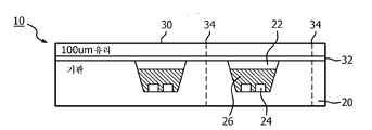
도 1은 개별화 이전의 웨이퍼의 부분의 단면도이고, 이때 기판은 캐비티들을 가지고, 각각의 캐비티는 하나 이상의 LED 다이를 포함한다. 캐비티들은 파장 변환 재료에 의해 채워지고, 캐비티들은 평탄한 투명 플레이트에 의해 기밀하게 밀봉된다.
도 2는 각각의 캐비티 주위의 밀봉을 도시하는, 도 1의 웨이퍼의 부분의 상부면도이다(용이한 식별을 위해 밀봉은 상당히 좁게 도시된다).
도 3은 개별화 이전의 웨이퍼의 부분의 단순화된 단면도이고, 이때 기판은 실질적으로 평탄하고 LED 다이들을 지지하며, 파장 변환 재료는 LED 다이들을 캡슐화하기 위하여 각각의 LED 다이 상에 몰딩되고, 투명 플레이트는 캐비티들을 가지며, 기밀 밀봉은 각각의 캐비티 주위에 형성된다.
도 4는 각각의 플레이트 캐비티 주위의 밀봉을 도시하는, 도 3의 웨이퍼의 부분의 상부면도이다.
도 5는 광 방출을 성형하는 광학적 패턴을 가지는 단일의 개별화된 LED 모듈에 대한 플레이트의 부분의 단면도이다. 광학적 패턴은 렌즈들, 광 스캐터링 피쳐들, 반사체들, 광 흡수체들을 형성할 수 있거나, 임의의 다른 피쳐들을 형성할 수 있다.
도 6은 도 5의 플레이트 부분의 상부면도이다.
도 7은 광 방출을 중심 영역에 집중시키기 위하여 단일 LED 다이 영역 주위에 형성된 반사체 링(reflective ring)을 도시하는, 단일의 개별화된 LED 모듈에 대한 플레이트의 부분의 단면도이다.
도 8은 도 7의 플레이트 부분의 상부면도이다.
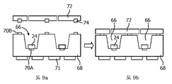
도 9a 및 도 9b는 웨이퍼의 부분의 단면도들이고, 이때 LED 다이들은 기판의 캐비티들 내에 마운팅되고 저온의 AuSn 솔더에 의한 것과 같이 열을 사용하여 금속-접합되며, 플레이트의 기밀 밀봉이 동일한 솔더를 사용하여 동시에 형성된다.
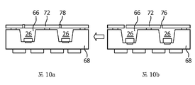
도 10a는 도 9b의 구조체 내의 캐비티들이 다음으로 플레이트 내의 개구들을 통해 파장 변환 재료에 의해 채워지고, 이로써 파장 변환 재료가 도 9b의 솔더 가열 단계를 피하는 방법을 도시한다.
도 10b는 플레이트 내의 개구들이 다음으로 기밀 밀봉을 완료하기 위하여 채워지는 방법을 도시한다.
도 11은 파장 변환 재료를 포함하는 수직형 실린더들을 형성하는 복수의 밀봉된 캐비티를 가지는, 단일의 개별화된 LED 모듈을 위한 플레이트의 부분의 상부면도이다.
도 12는 도 11의 선(12-12)을 따라 보여지는 도 11의 플레이트를 사용하는 개별화 이후의 단일 LED 모듈의 단면도이고, 이때 파장 변환 재료는 플레이트 내의 캐비티들을 채우고, 플레이트는 추가적인 파장들을 생성하기 위하여 선택적인 인광체 층에 의해 덮여진다.
도 13은 플레이트 내의 캐비티들이 개별화 이후에 밀봉되는 파장 변환 재료에 의해 채워진 수평형 실린더들인 것을 제외하고 도 11과 유사하다.
도 14는 도 13의 선(14-14)을 따라 보여지는 도 13의 플레이트를 사용하는 개별화 이후의 단일 LED 모듈의 단면도이고, 이때 파장 변환 재료는 캐비티들을 채우고, 플레이트는 캐비티들의 종단들을 밀봉하기 위하여 (인광체 입자들을 포함하는) 봉합재에 의해 덮여진다.
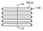
도 15는 모세관 작용(capillary action)에 의해 파장 변환 재료에 의해 채워진 세라믹 또는 유리로 이루어진 속이 빈 스트립들(hollow strips)의 상부면도이다. 대안적으로, 서브-플레이트(sub-plate)는 파장 변환 재료로 채워진 수평형 캐비티들을 포함할 수 있다.
도 16은 도 15의 선(16-16)을 따라 보여지는 도 16의 스트립들 또는 서브-플레이트를 사용하는 개별화 이후의 단일 LED 모듈의 단면도이고, 이때 스트립들 또는 서브-플레이트는 상부 플레이트에 접합되고, 그것은 LED 다이들을 포함하는 캐비티들을 가지는 기판에 다음으로 접합된다. 접합은 기밀 밀봉을 생성한다. 요구되는 경우, 수평형 캐비티들의 종단들은 다음으로 봉합재에 의해 기밀하게 밀봉된다.
동일하거나 유사한 요소들은 동일한 참조번호에 의해 나타내어진다.BRIEF DESCRIPTION OF THE DRAWINGS Figure 1 is a cross-sectional view of a portion of a wafer prior to individualization, wherein the substrate has cavities and each cavity comprises one or more LED dies. The cavities are filled by the wavelength converting material, and the cavities are hermetically sealed by a flat transparent plate.
Figure 2 is a top view of the portion of the wafer of Figure 1 showing sealing around each cavity (the seal is shown to be fairly narrow for easy identification).
Figure 3 is a simplified cross-sectional view of a portion of the wafer prior to customization, wherein the substrate is substantially planar and supports the LED dies, the wavelength conversion material is molded onto each LED die to encapsulate the LED dies, Cavities, and a hermetic seal is formed around each cavity.
Figure 4 is a top view of a portion of the wafer of Figure 3 showing sealing around each plate cavity.
5 is a cross-sectional view of a portion of a plate for a single, customized LED module having an optical pattern for shaping light emission. The optical pattern can form lenses, optical scattering features, reflectors, light absorbers, or any other features.
Figure 6 is a top view of the plate portion of Figure 5;
7 is a cross-sectional view of a portion of a plate for a single, customized LED module showing a reflective ring formed around a single LED die area to focus light emission onto a central area.
Figure 8 is a top view of the plate portion of Figure 7;
Figures 9a and 9b are cross-sectional views of portions of the wafer where the LED dies are mounted within the cavities of the substrate and are metal-bonded using heat, such as by cold AuSn solder, and the airtight seal of the plate uses the same solder Respectively.
FIG. 10A shows how the cavities in the structure of FIG. 9B are then filled by the wavelength conversion material through openings in the plate, thereby avoiding the wavelength conversion material in FIG. 9B, the solder heating step.
Figure 10B shows how the openings in the plate are then filled to complete a hermetic seal.
11 is a top view of a portion of a plate for a single, customized LED module having a plurality of sealed cavities forming vertical cylinders comprising a wavelength converting material.
12 is a cross-sectional view of a single LED module after individualization using the plate of FIG. 11 taken along line 12-12 of FIG. 11, wherein the wavelength converting material fills the cavities in the plate and the plate creates additional wavelengths Lt; RTI ID = 0.0 > phosphor layer. ≪ / RTI >
Figure 13 is similar to Figure 11 except that the cavities in the plate are horizontal cylinders filled with a wavelength conversion material that is sealed after individualization.
14 is a cross-sectional view of a single LED module after individualization using the plate of FIG. 13 taken along line 14-14 of FIG. 13, wherein the wavelength conversion material fills the cavities and the plate encapsulates the ends of the cavities (Including the phosphor particles).
Figure 15 is a top view of hollow strips of ceramic or glass filled by a wavelength converting material by capillary action. Alternatively, the sub-plate may comprise horizontal cavities filled with a wavelength conversion material.
Figure 16 is a cross-sectional view of a single LED module after individualization using the strips or sub-plates of Figure 16 shown along line 16-16 of Figure 15, wherein the strips or sub- Which is then bonded to a substrate having cavities containing LED dies. The joint creates a hermetic seal. If desired, the ends of the horizontal cavities are then hermetically sealed by the sealant.
The same or similar elements are denoted by the same reference numerals.
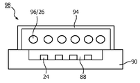
도 1은 개별화 이전의 웨이퍼(10)의 부분을 도시한다. 웨이퍼(10)는 기판(20) 및 투명 플레이트(30)를 포함한다. 기판(20)은 높은 열 전도성 재료로 형성된다. 기판(20)은 예를 들어 사파이어, 스피넬(spinel), 또는 다결정 알루미나와 같은 투명 세라믹으로 형성될 수 있다. 기판(20)은 또한 세라믹 분말이 몰딩되고 압력 하에서 소결된(sintered), 몰딩된 세라믹 재료를 포함하는 임의의 다른 투명 또는 비-투명 세라믹 재료로 형성될 수 있다. 다른 실시예들에서, 기판(20)은 유리-세라믹일 수 있다. 다른 실시예에서, 기판(20)은 탄성중합체 바디(elastomer body) 내에 매입된 금속 리드 프레임일 수 있다.Figure 1 shows a portion of the
도 1에서, 기판(20)은 캐비티들(22)을 가지도록 몰딩되거나 절삭된다(machined). 기판(20)이 광 흡수 재료로 형성되는 경우, 캐비티(22) 벽들은 (바람직하게 가시광선에 대해 적어도 90% 반사성인) 반사성 필름에 의해 코팅될 수 있다. 기판(20)은 백색 세라믹 재료(white ceramic material)와 같은 반사성 재료로도 형성될 수 있다. 대안적으로, 필름 또는 기판(20)의 반사성은 예를 들어 UV 광과 같은 비-가시 광에 대한 것일 수 있다.In FIG. 1, the
개별화된 LED 모듈들을 인쇄 기판 회로(PCB) 또는 다른 기판에 솔더링하기 위해, 각각의 캐비티(22)의 바닥은 기판(20) 상에 종래의 하부 금속 패드들(도시되지 않음)에 전기적으로 연결되는 종래의 전극들(도시되지 않음)을 가진다. 캐비티 전극들은 플립 칩 LED들, 수직형 LED들 등과 같이 사용된 특정한 LED 다이들(24) 상의 전극들에 대응하도록 위치된다. 기판(20)은 비아들(vias)을 포함하도록 몰딩될 수 있고, 종래의 기술들을 사용하여 캐비티들(22) 내에 다양한 전극들을 형성하고, 비아들을 채우며, 기판(20)의 바닥 표면 상에 금속 패드들을 형성하도록, 금속이 퇴적되고 패턴화된다. 전극들은 LED 다이들(24)과 기판(20) 사이의 열 전도성 경로를 제공한다. 전기적으로 절연된 금속 열 패드가 또한 LED 다이들(24)의 바닥 상에 위치될 수 있고 캐비티들(22) 내의 금속 열 패드에 접합될 수 있다.The bottom of each
기판(20)이 다공성 표면(porous surface)과 같이 불량한 접착력(adhesion)을 제공하는 상부 표면을 가지는 경우, 기판(20)과 (이하에서 설명되는) 상부 플레이트 사이의 더 나은 기밀 밀봉을 성취하기 위하여, 밀봉 층(sealant layer)과 같은 상부 층이 기판(20) 표면 상에 퇴적될 수 있다.In order to achieve a better hermetic seal between the
일 실시예에서, LED 다이들(24)은 청색 광을 방출하는 고휘도 LED 다이들이다. 그러한 LED 다이들(24)은 비교적 고열을 생성하고, 그러한 열은 전도를 통해 기판(20) 및 나중에 기판(20)이 마운팅되는 PCB에 의해 확산되고 제거될 필요가 있다. 수평적으로 그리고 다음으로 상향으로 수직하게 기판(20)을 통해 전도된 열은 바람직하게는 임의의 덮인 구조체(overlying structure)에 의해 차단되지 않고, 이에 의해 기판(20) 위의 주변 공기가 또한 전도 및/또는 대류에 의해 열을 제거할 수 있다.In one embodiment, the LED dies 24 are high-brightness LED dies that emit blue light. Such LED dies 24 produce relatively high heat and such heat needs to be diffused and removed by conduction through the
도 1에서, 4개의 LED 다이(24)가 추가적인 휘도를 위해 각각의 캐비티(22) 내에 마운팅되지만, 단면에서는 캐비티(22) 마다 2개만이 단면에서 도시된다.In Fig. 1, four LED dies 24 are mounted within each
캐비티들(22)은 다음으로 파장 변환 재료(26)에 의해 채워지거나 부분적으로 채워진다. 그러한 재료(26)는 일반적으로 바인더 내의 인광체 분말 또는 캐리어 내에 분산된 양자 점들일 것이다. 양자 점들을 위한 캐리어는 또한 바인더로서 지칭될 수 있다. 서브-마이크로 크기인 양자 점들은 정주하지 않고 바인더 내에 상당히 잘 분산된 채로 남아있다. 투명 바인딩 재료는 실리콘과 같은 폴리머일 수 있다. 많은 종류들의 인광체들 및 양자 점들은 고열에 의해 성능이 저하되고, 따라서 본 발명의 하나의 목적은 파장 변환 재료의 가열을 제한하는 한편, 열이 LED 다이로부터 제거되는 것을 가능하게 하는 구조를 제공하는 것이다.The
각각의 캐비티(22)의 부피는 각각의 LED 다이(24)의 부피보다 더욱 더 크다. 이에 따라, 파장 변환 재료(26)의 부피는 비교적 크고, 그에 의해 인광체 입자들 또는 양자 점들이 낮은 농도를 가질 수 있게 한다. 파장 변환 재료(그것의 바인더를 포함)의 열 전도율은 기판(20)의 열 전도율보다 자릿수가 더 낮다(예를 들어, 0.1 내지 0.2W/mK 대비 30W/mK). 따라서, 파장 변환 재료(26)의 큰 부피 및 낮은 열 전도율은 인광체 입자들 또는 양자 점들로 전도되는 열을 제한한다. 즉, 재료(26) 내의 열 확산 길이(heat diffusion length)가 매우 짧다. 따라서, 인광체 입자들 또는 양자 점들이 파장 변환 재료(26) 전반에서 분산되는 경우, 그들은 LED 다이들(24)에 의해 생성된 고열에도 불구하고, 크게 성능이 저하되지는 않는다.The volume of each
추가적으로, 양자 점들이 카드뮴과 같은 독성 요소들을 포함하는 경우, RoHS 표준(소정의 유해 물질들의 사용의 제한)은 기준을 충족시키기 위하여 양자 점 필름 내의 카드뮴 금속의 희석을 요구한다. 이것은 {원하는 온-백색 점(warm-white color point)과 같은} 원하는 색 방출을 여전히 유지하면서, 바인더의 부피를 증가시키고, 양자 점 농도를 감소시킴으로써 성취될 수 있다.Additionally, if the quantum dots contain toxic elements such as cadmium, the RoHS standard (restriction of the use of certain hazardous materials) requires dilution of the cadmium metal in the quantum dots film to meet the criteria. This can be accomplished by increasing the volume of the binder and decreasing the quantum dot concentration while still maintaining the desired color emission (such as the desired warm-white color point).
파장 변환 재료(26)의 상부와 캐비티(22)의 상부 사이의 임의의 보이드(void)는 공기 주머니들 및 부차적 반사 영향들을 방지하기 위하여 투명 바인더 재료에 의해 채워질 수 있다.Any voids between the top of the
다음으로, 평탄한 투명 세라믹, 유리, 또는 탄성중합체 플레이트(30)가 제공된다. 다른 재료가 또한 적합할 수 있다. 플레이트(30)는 기판(20) 웨이퍼와 대략 동일한 크기일 것이다. 일 실시예에서, 플레이트는 광 흡수를 최소화하고 주변 공기에 대한 높은 열 전도성 경로를 생성하기 위하여 약 100 마이크로미터 두께이다.Next, a flat transparent ceramic, glass, or
투명 밀봉 재료(32)는 각각의 캐비티(22)를 둘러싸도록 예를 들어 스크린 프린팅(screen printing)에 의해 플레이트(30) 및/또는 기판(20) 상에 퇴적된다. 열이 플레이트(30) 및 주변 공기로 전도되도록, 밀봉 재료(32)는 양질의 열 전도성을 가지고 넓은 영역을 덮어야 할 것이다. 밀봉 재료(32)는 저온 유리, 유리 프릿(glass frit), 금속, 금속 산화물, 높은 열 전도성 에폭시, 또는 기밀 밀봉을 형성할 수 있는 다른 적합한 재료일 수 있다. 일 실시예에서, 밀봉 재료(32)는 기밀 밀봉을 생성하기 위하여 레이저 어닐링, 레이저 가열, 오븐 가열, 또는 광학적 경화(optically curing)에 의해 가열되거나 경화된다. 밀봉 재료(32) 및 다른 재료들은 동작 도중의 박리(delamination)를 방지하기 위하여 유사한 열 팽창 계수들을 가지도록 선택되어야 할 것이다.A
밀봉 프로세스는 캐비티들(22)로부터 공기를 제거하기 위하여 진공 내에서 수행될 수 있고, 하향 압력이 플레이트(30)에 인가될 수 있다.The sealing process may be performed in a vacuum to remove air from the
결과적인 웨이퍼는 다음으로 개별 LED 모듈들을 형성하기 위하여 선들(34)을 따라 예를 들어, 소잉(sawing)에 의해 개별화된다. 청색광 및 파장 변환 재료(26)에 의해 생성된 광의 조합은 사실상 어떠한 색의 광이든 생성할 수 있다.The resulting wafer is then individualized by, for example, sawing along the
모두 높은 열 전도성 재료인 기판(20), 밀봉 재료(32), 및 플레이트(30)의 조합은 주변 공기 및 열 전도성 인쇄 회로 기판(예를 들어, 금속 바디를 가지는 회로 기판)으로 열을 전도함으로써 LED 다이들(24)로부터의 열을 제거하고, 이는 낮은 열 전도성 파장 변환 재료(26)의 대부분 또는 전부가 성능이 저하되는 것을 방지하기 위해 대부분의 파장 변환 재료들에 대하여 적합한 130℃ 미만에 남아있는 것을 가능하게 한다.The combination of the
밀봉 재료(32)는 고선속 청색광으로부터 멀리 떨어져있고, 캐비티들(22) 내의 불투명 반사성 층은 밀봉 재료(32)에 부딪히는 광을 차단할 것이기 때문에, 밀봉 재료(32)가 고선속을 견뎌야 할 필요는 줄어든다.The need for the sealing
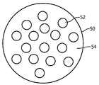
도 2는 각각의 캐비티(22) 주위의 밀봉 재료(32)의 가능한 위치를 도시하는, 도 1의 웨이퍼(10)의 부분의 상부면도이다. 밀봉 재료(32)는 그것의 위치를 도시하기 위하여 일반적인 실시예에 대하여 스케일되지 않은 좁은 "비드(bead)"로서 도시된다. 다른 실시예에서, 플레이트(30)의 전체 표면은 기판(20)에 대한 열 전도성을 증가시키기 위하여 밀봉 재료(32)에 의해 코팅된다.Figure 2 is a top view of the portion of the
도 3은 개별화 이전의 웨이퍼(40)의 작은 부분의 단순화된 단면도이고, 이때 기판(42)은 실질적으로 평탄하고 LED 다이들(24)을 지지한다. LED 다이들(24)은 종래의 금속 전극들(애노드 및 캐소드)을 가지고, 이들은 도 1에 관하여 논의된 것과 같이 기판(42) 상의 대응하는 전극들에 전기적으로 그리고 열적으로 연결된다.3 is a simplified cross-sectional view of a small portion of the
(웨이퍼로서의) 기판(42)은 경화되지 않은 파장 변환 재료(26)에 의해 채워진 캐비티들을 가지는 몰드와 마주한다. 파장 변환 재료(26)는 LED 다이들(24)을 캡슐화한다. 재료(26)는 다음으로 경화하고, 기판(42)은 몰드로부터 릴리즈된다. 바람직하게, 결과적인 몰딩된 재료(26)는 비교적 두껍고, 낮은 농도의 인광체 입자들 또는 양자 점들을 낮은 열 전도성 투명 바인더 내에 가지며, 이에 의해 인광체 입자들 또는 양자 점들 중 대부분 또는 전부는 고열에 노출되지 않는다.The substrate 42 (as a wafer) faces the mold with the cavities filled by the uncured
유리 또는 세라믹으로 형성되는 것과 같은 투명 플레이트(44)가 몰딩되거나, 절삭되거나, 에칭되거나, 그렇지 않으면 캐비티들(46)을 가지도록 형성된다. 진공 하에서, 플레이트(44)는 밀봉 재료(32)에 의해 기판(42)에 대하여 밀봉되고, 이는 도 1에 관하여 설명된 것과 동일할 수 있으며, 동일한 방식으로 경화된다. 바람직하게, LED 다이들(24)이 동작 도중에 열을 생성하는 경우, 박리를 방지하기 위하여, 몰딩된 재료(26)와 캐비티들(46)의 상부 사이의 갭 내의 공기의 양은 최소화되어야 할 것이다. 웨이퍼는 다음으로 선들(34)을 따라 개별화된다.A
사용된 밀봉 재료(32), 넓은 범위에 걸친 밀봉 재료(32)의 확산, LED 다이들(24)로부터의 열 및 선속의 분산, 기판(42) 및 플레이트(44)의 높은 열 전도율, 및 파장 변환 재료(26)의 낮은 전도율 및 큰 부피로 인하여, 밀봉은 높은 열 및 선속에서 신뢰성을 가지고, 인광체 또는 양자 점들은 고열에 노출되지 않는다.The diffusion of the sealing
모든 실시예들에서, 기판 및 상부 플레이트를 포함하는 높은 열 전도성 재료들은 20 W/mK 초과의 전도율을 가져야 할 것이다. 밀봉 재료가 매우 얇을 것이기 때문에, 그것의 열 전도율이 중요하지는 않지만, 높은 것이 바람직할 것이다.In all embodiments, the high thermal conductivity materials including the substrate and the top plate will have a conductivity of greater than 20 W / mK. Since the sealing material will be very thin, its thermal conductivity is not critical, but a higher one would be desirable.
평탄한 기판(42)은 바람직하게 그것의 상부 표면 상에 반사성 층을 가지고, 이는 광을 상향으로 반사하도록 정 반사성이거나 확산 반사성일 수 있다. 반사성 층은 금속, 흰색 페인트 등일 수 있다.The
도 4는 각각의 플레이트 캐비티(46) 주위의 밀봉 재료(32) 위치를 도시하는, 도 3의 웨이퍼(40)의 작은 부분의 상부면도이다. 밀봉 재료(32)는 도 3에 도시된 것과 같이 더 넓은 범위에 걸쳐 분포되지만, 밀봉의 일반적 위치를 더 잘 도시하기 위하여, 도 4에서 도시된 일반적인 실시예에 대하여 스케일되지 않는 좁은 "비드"로서 도시된다.4 is a top view of a small portion of the
도 5는 단일의 개별화된 LED 모듈에 대한 플레이트(50)의 단면도이다. 플레이트(50)의 바닥은 도 1 또는 도 3에서 도시된 것처럼 기판에 대하여 밀봉될 것이다. 플레이트(50)의 바닥은 평탄하거나 캐비티들을 가질 수 있다. 도 5는 플레이트(50)가, 예를 들어 광을 스캐터링하거나, 렌즈들을 형성하거나, 광을 재지향하거나, 광을 흡수하거나, 광을 반사할 수 있는 광학적 피쳐들(52)을 포함할 수 있는 것을 나타내기 위하여 의도된다. 도 5 및 도 6의 단순화된 예시에서, 광학적 피쳐들(52)은 원통형 오목부들(cylindrical indentations)이다.5 is a cross-sectional view of the
도 6은 도 5에서 도시된 플레이트(50)의 상부면도이고, 이때 광학적 피쳐들(52)은 플레이트(50) 내의 원형 오목부들로서 도시된다. 대부분의 광이 원형 오목부들을 통해 거의 독점적으로 방출되도록, 플레이트(50)는 또한 다른 영역들 상에 반사성 필름(54)을 포함할 수 있다. 플레이트(50)에 비-평면 상부 표면을 제공함으로써, 내부 반사가 감소된다. 다른 실시예에서, 오목부들은 광 추출을 증가시키기 위한 각진 프리즘들(angled prisms)이다. 플레이트(50)는 원형으로서 도시되지만, 직사각형 또는 임의의 다른 적합한 형상일 수 있다.6 is a top view of the
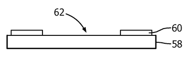
도 7은 광 방출을 중심 영역(62)으로 제한하도록 단일 LED 다이 영역 주위에 형성된 반사성 링(60)을 도시하는, 단일의 개별화된 LED 모듈에 대한 플레이트(58)의 단면도이다. 플레이트(58)의 바닥은 평탄할 수 있거나 캐비티들을 가질 수 있고, 위에서 설명된 것처럼 기판에 대하여 밀봉된다. 링(60)은 알루미늄, 은, 또는 다른 반사성 재료로 퇴적될 수 있다. 링(60)의 바닥 표면에 부딪히는 LED 광선들은 하향으로 지향되고, 도 3의 기판(42)과 같은 기판의 반사성 표면으로 다시 반사되어 올라온다.Figure 7 is a cross-sectional view of the
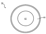
도 8은 반사성 링(60) 및 투명 중심 영역(62)을 도시하는, 도 7의 플레이트(58)의 상부면도이다. 플레이트(58)는 또한 직사각형 또는 임의의 다른 적합한 형상일 수 있다.8 is a top view of the
도 9a 및 도 9b는 LED 다이들(24)이 기판(68)의 캐비티들(66) 내에 마운팅되고 저온의 AuSn 솔더(70A)에 의한 것과 같이 열을 사용하여 기판 전극들과 금속-접합되며, 플레이트(72)의 기밀 밀봉이 동일한 솔더(70B)를 사용하여 동시에 형성되는, 웨이퍼의 부분의 단면도들이다. LED 다이들(24)을 기판 전극들에 접합하는 솔더(70A)는 기판(68) 상의 종래의 애노드 및 캐소드 하부 패드들(71)에 대한 전기적 전도성을 제공하고, 또한 기판(68) 바디에 대한 열적 전도성을 제공한다. 전기적으로 절연된 넓은 열 패드가 또한 제공될 수 있다. 플레이트(72)는 금속 링들(74)을 제공받고, 이는 기판(68)과의 기밀 밀봉을 형성하기 위하여 솔더(70B)와 접합된다.9A and 9B illustrate that the LED dies 24 are mounted within the
상부 플레이트(72)와 기판(68) 사이에서 양질의 열 전도성을 갖는 넓은 밀봉을 제공하기 위하여, 솔더(70B) 및 금속 링(74)은 도 9a 및 도 9b에서 도시된 것보다도 훨씬 더 넓을 수 있다.
도 10a는 도 9b의 기판(68) 내의 캐비티들(66)이 다음으로 플레이트(72) 내의 작은 개구들(76)을 통해 (공기 갭들을 방지하기 위하여) 파장 변환 재료(26)에 의해 실질적으로 완전히 채워지고, 이에 의해 파장 변환 재료(26)가 도 9b의 솔더(70) 가열 단계를 피하는 방법을 도시한다. 인광체 입자들 또는 양자 점들의 온도를 제한하기 위하여, 파장 변환 재료(26)는 비교적 큰 부피를 가지고, 낮은 열 전도율을 가지며, 낮은 농도의 인광체 입자들 또는 양자 점들을 가진다. 대안적인 실시예에서, 파장 변환 재료(26)가 도입됨에 따라, 각각의 캐비티(66)에 대해 공기의 탈출을 허용하기 위해 다수의 개구(76)가 사용된다. 유사하게, 개구들(76) 중 일부는 변환 재료(26)를 캐비티들(66) 내로 "끌어당기기(pull)" 위하여 진공 소스에 연결될 수 있다.Figure 10a shows the
도 10b는 플레이트(72) 내의 개구들(76)이 다음으로 기밀 밀봉을 완료하기 위하여 다른 타입의 밀봉 재료(78)(예를 들어, 실리콘 또는 에폭시)에 의해 채워지는 방법을 도시한다.Figure 10B illustrates how the
다음으로, 결과적인 웨이퍼는 예를 들어 도 10b의 구조체의 중간을 통해서, 개별화될 수 있다.Next, the resulting wafer may be individualized, for example, through the middle of the structure of FIG. 10B.
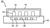
도 11은 파장 변환 재료(26)를 포함하는 수직형 실린더들을 형성하는 복수의 밀봉된 캐비티들(82)을 가지는, 단일의 개별화된 LED 모듈을 위한 플레이트(80)의 상부면도이다.Figure 11 is a top view of a
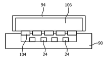
도 12는 도 11의 선(12-12)을 따라 보여지는, 도 11의 플레이트(80)를 사용하는 개별화 이후의 단일 LED 모듈(84)의 단면도이다. 파장 변환 재료(26)는 투명 밀봉 플레이트(86)에 의해 캐비티들(82) 내에서 밀봉되고, 이는 또한 LED 다이들(24)이 마운팅되는 기판(90) 내의 중심 캐비티(88) 주위에 기밀 밀봉을 형성할 수 있다. 위에서 설명된 임의의 밀봉 재료들은 캐비티(88)의 주변부 주위에서 사용될 수 있다. 선택적으로, 플레이트(80)는 추가적인 파장들을 생성하기 위하여 멀리 떨어진 인광체 층(94)에 의해 덮여진다. 다양한 파장 변환 재료들의 LED 다이들(24)로부터의 먼 거리로 인해, 재료들은 고온에 노출되지 않고 성능이 저하되지 않는다. 캐비티들(82) 중 임의의 하나의 밀봉 재료가 파손된 경우, 그것은 다른 캐비티들(82)에 대한 밀봉에 영향을 미치지 않는다.12 is a cross-sectional view of a single LED module 84 after individualization using the
도 13은 플레이트(98) 내의 캐비티들(96)이 파장 변환 재료(26)에 의해 채워진 수평형 실린더들인 것을 제외하고는 도 11과 유사하다. 캐비티들(96)은 플레이트(98)의 에지들까지 계속 연장되고, 캐비티들(96)의 개방 종단들은 실리콘 또는 에폭시와 같은 적합한 밀봉 재료(100)에 의해 밀봉된다. 캐비티들(96)은 모세관 작용에 의해 채워질 수 있다.13 is similar to Fig. 11 except that the cavities 96 in the
도 14는 도 13의 선(14-14)을 따라 보여지는, 도 13의 플레이트(98)를 사용하는 개별화 이후의 단일 LED 모듈의 단면도이다. 플레이트(98)는 도 12에 관하여 설명된 것과 동일한 기판(90)과 짝지어진다(mated). 기판 캐비티(88)를 둘러싸는 플레이트(98)의 주변부는 위에서 설명된 것과 같은 기밀 밀봉을 포함한다. 캐비티들(96)의 종단들의 밀봉은 플레이트(98) 상의 선택적 인광체 층(94) 내의 실리콘 바인더 재료에 의한 것일 수 있다.14 is a cross-sectional view of a single LED module after individualization using the
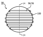
도 15는 모세관 작용에 의해 파장 변환 재료(26)에 의해 채워진 세라믹 또는 유리로 이루어진 속이 빈 스트립들(104)의 상부면도이다. 대안적으로 서브-플레이트는 파장 변환 재료(26)에 의해 채워진 수평 캐비티들을 포함할 수 있다.15 is a top view of
도 16은 도 15의 선(16-16)을 따라 보여지는, 도 15의 스트립들(104) 또는 서브-플레이트를 사용하는 개별화 이후의 단일 LED 모듈의 단면도이고, 이때 스트립들(104) 또는 서브-플레이트는 상부 플레이트(106)에 접합되고, 그것은 다음으로 LED 다이들(24)을 포함하는 캐비티들(88)을 가지는 기판(90)에 대하여 밀봉된다. 요구되는 경우, 수평형 캐비티들(104)의 종단들은 적합한 밀봉 재료(108)에 의해 기밀하게 밀봉된다(도 15). 선택적인 인광체 층(94)은 플레이트(106) 상에 퇴적될 수 있다.Figure 16 is a cross-sectional view of a single LED module after individualization using the
도 11 내지 도 16에서, 단일 LED 모듈에 대한 부분들이 도시된다. 그러나, 모듈들이 (개별화 이전에) 웨이퍼 레벨 프로세스 동안 상부 플레이트를 사용하여 밀봉되는 경우, 상부 플레이트 및 기판의 에지들은 도 1 및 도 3과 유사하게 개별화 이후의 LED 모듈들의 집합과 일치할 것이다. 이것은 LED 모듈의 비용을 상당히 감소시킨다.In Figures 11-16, portions for a single LED module are shown. However, when the modules are sealed using a top plate during a wafer level process (prior to personalization), the top plate and the edges of the substrate will coincide with the set of LED modules after individualization similar to Figs. This significantly reduces the cost of the LED module.
모든 실시예들에서, 본 명세서에서 설명된 다양한 인자들의 조합에 의하여 LED 다이에 의해 생성된 높은 열 및 선속에도 불구하고, 고휘도 LED 다이들에 의하더라도, 파장 변환 재료(26)의 온도는 비교적 낮게 유지되고, 밀봉 재료는 신뢰성 있는 기밀 밀봉을 제공한다.In all embodiments, despite the high thermal and linearity produced by the LED die by the combination of the various factors described herein, even with high-brightness LED dies, the temperature of the
바람직하게, 모든 실시예들에서, LED 모듈이 LED 다이를 동작시킴으로써 가열되는 경우의 박리를 방지하기 위하여, 캐비티 내에 갇힌 공기는 없다. 이것은 캐비티를 완전히 채우거나 진공에서 기밀 밀봉 단계를 수행함으로써 성취될 수 있다.Preferably, in all embodiments, there is no trapped air in the cavity to prevent delamination when the LED module is heated by operating the LED die. This can be accomplished by completely filling the cavity or by performing a hermetic sealing step in vacuum.
웨이퍼들로서의 기판에 대하여 상부 플레이트를 밀봉하고, 다음으로 웨이퍼를 개별화함으로써, 상부 플레이트의 에지들은 일반적으로 기판의 에지들과 일치할 것이다. 웨이퍼 프로세스 내에서 기밀 밀봉을 형성하는 것은 개별화 이후에 각각의 모듈을 밀봉하는 것보다도 훨씬 더 비용이 저렴하다. 따라서, 본 명세서에서 설명된 프로세스는 LED 모듈 당 매우 적은 초과 비용에 의해 수행될 수 있다.By sealing the top plate with respect to the substrate as wafers and then by customizing the wafer, the edges of the top plate will generally coincide with the edges of the substrate. Forming a hermetic seal within a wafer process is much less expensive than sealing each module after individualization. Thus, the process described herein can be performed with very little excess cost per LED module.
본 발명의 특정한 실시예들이 도시되고 설명되었더라도, 변화들 및 수정들이 그것의 더 넓은 태양들 내에서 본 발명으로부터 벗어남이 없이도 행해질 수 있고, 따라서 첨부되는 청구항들은 그들의 범주 내에 그러한 모든 변화들 및 수정들을 본 발명의 참된 정신 및 범주 내에 있는 것으로서 포함하는 것이 본 기술분야의 기술자들에게 명백할 것이다.Although specific embodiments of the present invention have been shown and described, changes and modifications may be made without departing from the invention in its broader aspects, and the appended claims are to be accorded the full scope of the present invention, It will be apparent to those skilled in the art to include the present invention within its true spirit and scope.
Claims (15)
제1 열 전도율(thermal conductivity)을 가지는 기판;
상기 기판 상에 전기적으로 그리고 열적으로 마운팅된 LED 다이;
상기 제1 열 전도율보다 실질적으로 더 낮은 제2 열 전도율을 가지는 파장 변환 재료(wavelength conversion material) - 상기 파장 변환 재료는 상기 LED 다이를 덮게(overlying) 위치됨 -;
상기 제2 열 전도율보다 더 큰 제3 열 전도율을 가지는 광 투과성 상부 플레이트(light transmitting top plate) - 상기 상부 플레이트는 상기 파장 변환 재료 상에 위치됨 -; 및
상기 LED 다이 및 상기 파장 변환 재료를 둘러싸는 상기 기판과 상기 상부 플레이트 사이에서 밀봉 재료(sealant material)에 의해 형성된 기밀 밀봉(hermetic seal)
을 포함하고,
상기 상부 플레이트 및 상기 기판이 웨이퍼 레벨 프로세스(wafer level process) 동안 밀봉되고 다음으로 웨이퍼가 상기 LED 모듈을 형성하기 위하여 개별화되는(singulated) 것으로 인하여, 상기 상부 플레이트의 에지들 및 상기 기판의 에지들이 일치하며,
상기 LED 다이는 상기 기판 또는 상기 상부 플레이트의 캐비티(cavity) 내에 위치되는, LED 모듈.As a light emitting diode (LED) module,
A substrate having a first thermal conductivity;
An electrically and thermally mounted LED die on the substrate;
A wavelength conversion material having a second thermal conductivity that is substantially lower than the first thermal conductivity, the wavelength conversion material being located overlying the LED die;
A light transmitting top plate having a third thermal conductivity greater than the second thermal conductivity, the top plate being positioned on the wavelength conversion material; And
A hermetic seal formed by a sealant material between the LED die and the top plate surrounding the wavelength converting material,
/ RTI >
The edges of the top plate and the edges of the substrate match because the top plate and the substrate are sealed during a wafer level process and then the wafer is singulated to form the LED module In addition,
Wherein the LED die is located within a cavity of the substrate or the top plate.
상기 기판은 상기 LED 다이가 위치되는 상기 캐비티를 가지는, LED 모듈.The method according to claim 1,
Wherein the substrate has the cavity in which the LED die is located.
상기 상부 플레이트는 상기 LED 다이가 위치되는 상기 캐비티를 가지는, LED 모듈.The method according to claim 1,
The top plate having the cavity in which the LED die is located.
상기 상부 플레이트는 유리를 포함하고, 상기 밀봉 재료는 상기 상부 플레이트를 상기 기판에 부착하기 위하여 용융된(melted) 유리를 포함하는, LED 모듈.The method according to claim 1,
Wherein the top plate comprises glass and the sealing material comprises melted glass for attaching the top plate to the substrate.
상기 밀봉 재료는 금속 솔더(metal solder)를 포함하고, 상기 LED 다이는 동일한 상기 금속 솔더를 사용하여 기판 전극(substrate electrode)에 접합되며, 상기 기밀 밀봉은 상기 기판이 상기 금속 솔더를 용융시키기 위하여 가열될 때 형성되는, LED 모듈.The method according to claim 1,
Wherein the sealing material comprises a metal solder and the LED die is bonded to a substrate electrode using the same metal solder, the hermetic seal being formed by heating the substrate to heat the metal solder The LED module being formed.
상기 캐비티를 상기 파장 변환 재료에 대한 몰드(mold)로서 사용하여, 상기 파장 변환 재료가 상기 캐비티 내로 퇴적되는(deposited), LED 모듈.The method according to claim 1,
Using the cavity as a mold for the wavelength conversion material, the wavelength conversion material being deposited in the cavity.
상기 캐비티를 상기 파장 변환 재료에 대한 몰드로서 사용하여, 상기 파장 변환 재료가 상기 캐비티 내로 퇴적되고, 상기 상부 플레이트는 상기 기밀 밀봉이 형성된 이후에 상기 파장 변환 재료를 상기 캐비티 내로 퇴적하기 위한 개구들(openings)을 가지는, LED 모듈.The method according to claim 1,
Using the cavity as a mold for the wavelength conversion material, the wavelength conversion material is deposited into the cavity, and the top plate includes apertures for depositing the wavelength conversion material into the cavity after the hermetic seal is formed openings.
상기 상부 플레이트는 웨이퍼로서의 상기 기판에 대하여 기밀하게 밀봉되고, 상기 웨이퍼는 상기 LED 모듈을 형성하기 위하여 개별화되는, LED 모듈.The method according to claim 1,
Wherein the top plate is hermetically sealed to the substrate as a wafer and the wafer is individualized to form the LED module.
상기 상부 플레이트는 상기 LED 다이에 의해 방출된 광을 재지향하는 광학적 피쳐들(optical features)을 가지는, LED 모듈.The method according to claim 1,
Wherein the top plate has optical features that redirect light emitted by the LED die.
상기 캐비티는 상기 파장 변환 재료를 포함하는 상기 상부 플레이트 내의 복수의 캐비티들 중 하나이고, 각각의 상기 캐비티들은 하나의 캐비티의 기밀 밀봉의 파손(break)이 다른 캐비티의 기밀 밀봉을 파손하지 않도록 밀봉되는, LED 모듈.The method according to claim 1,
Wherein the cavity is one of a plurality of cavities in the top plate that includes the wavelength converting material and each of the cavities is sealed so that break of the airtight seal of one cavity does not break the airtight seal of the other cavity , LED module.
상기 상부 플레이트는 제1 표면 및 제2 표면을 가지고, 상기 제1 표면은 캐비티들을 가지며, 상기 캐비티들은 상기 제2 표면에 실질적으로 수직인, LED 모듈.11. The method of claim 10,
The top plate having a first surface and a second surface, the first surface having cavities, the cavities being substantially perpendicular to the second surface.
상기 상부 플레이트는 제1 표면 및 제2 표면을 가지고, 상기 제1 표면은 캐비티들을 가지며, 상기 캐비티들은 상기 제2 표면에 실질적으로 평행인, LED 모듈.11. The method of claim 10,
The top plate having a first surface and a second surface, the first surface having cavities and the cavities substantially parallel to the second surface.
상기 캐비티는 상기 파장 변환 재료를 포함하는 복수의 캐비티들 중 하나이고, 상기 캐비티들은 별개의 상부 플레이트 부분 내에 형성되며 상기 상부 플레이트에 부착되고, 후속하여 상기 기밀 밀봉이 형성되는, LED 모듈.The method according to claim 1,
Wherein the cavity is one of a plurality of cavities comprising the wavelength converting material and wherein the cavities are formed in a separate top plate portion and attached to the top plate and subsequently the hermetic seal is formed.
상기 파장 변환 재료는 바인더(binder) 내의 인광체 입자들(phosphor particles) 또는 바인더 내의 양자 점들(quantum dots) 중 적어도 하나를 포함하는, LED 모듈.The method according to claim 1,
Wherein the wavelength conversion material comprises at least one of phosphor particles in a binder or quantum dots in a binder.
상기 LED 다이에 의해 생성된 열은 상기 기판, 상기 밀봉 재료, 및 상기 상부 플레이트의 열 전도에 의해 적어도 부분적으로 제거되고, 상기 파장 변환 재료의 온도는 상기 LED 다이의 온도보다 더 낮게 유지되는, LED 모듈.The method according to claim 1,
Wherein heat generated by the LED die is at least partially removed by thermal conduction of the substrate, the sealing material, and the top plate, and the temperature of the wavelength conversion material is maintained lower than the temperature of the LED die. module.
Applications Claiming Priority (3)
| Application Number | Priority Date | Filing Date | Title |
|---|---|---|---|
| US201361763081P | 2013-02-11 | 2013-02-11 | |
| US61/763,081 | 2013-02-11 | ||
| PCT/IB2014/058875 WO2014122626A1 (en) | 2013-02-11 | 2014-02-10 | Led module with hermetic seal of wavelength conversion material |
Publications (1)
| Publication Number | Publication Date |
|---|---|
| KR20150119179A true KR20150119179A (en) | 2015-10-23 |
Family
ID=50151344
Family Applications (1)
| Application Number | Title | Priority Date | Filing Date |
|---|---|---|---|
| KR1020157024839A KR20150119179A (en) | 2013-02-11 | 2014-02-10 | Led module with hermetic seal of wavelength conversion material |
Country Status (7)
| Country | Link |
|---|---|
| US (3) | US10002855B2 (en) |
| EP (1) | EP2954566B1 (en) |
| JP (2) | JP2016507162A (en) |
| KR (1) | KR20150119179A (en) |
| CN (2) | CN110010742B (en) |
| TW (1) | TWI645583B (en) |
| WO (1) | WO2014122626A1 (en) |
Cited By (1)
| Publication number | Priority date | Publication date | Assignee | Title |
|---|---|---|---|---|
| WO2017171196A1 (en) * | 2016-03-28 | 2017-10-05 | Samsung Electronics Co., Ltd. | Light emitting diode apparatus and manufacturing method thereof |
Families Citing this family (20)
| Publication number | Priority date | Publication date | Assignee | Title |
|---|---|---|---|---|
| KR102294837B1 (en) * | 2013-08-16 | 2021-08-26 | 삼성전자주식회사 | Methods for making optical components, optical components, and products including same |
| US10374137B2 (en) * | 2014-03-11 | 2019-08-06 | Osram Gmbh | Light converter assemblies with enhanced heat dissipation |
| DE102014108282A1 (en) * | 2014-06-12 | 2015-12-17 | Osram Opto Semiconductors Gmbh | Optoelectronic semiconductor component, method for producing an optoelectronic semiconductor component and light source with an optoelectronic semiconductor component |
| US9481572B2 (en) * | 2014-07-17 | 2016-11-01 | Texas Instruments Incorporated | Optical electronic device and method of fabrication |
| TW201624776A (en) * | 2014-12-18 | 2016-07-01 | Edison Opto Corp | LED lighting module |
| US20180301605A1 (en) * | 2015-03-19 | 2018-10-18 | Osram Opto Semiconductors Gmbh | A window that covers an optoelectronic semiconductor chip, a panel comprising a plurality of windows, a method of producing windows and an optoelectronic semiconductor device |
| CN107810565A (en) * | 2015-06-26 | 2018-03-16 | 康宁股份有限公司 | Sealing device and its manufacture method comprising quantum dot |
| DE102015111910A1 (en) * | 2015-07-22 | 2017-01-26 | Osram Opto Semiconductors Gmbh | Optoelectronic component, composite of optoelectronic components and method for producing an optoelectronic component |
| EP3334700A1 (en) * | 2015-08-12 | 2018-06-20 | Corning Incorporated | Sealed devices and methods for making the same |
| KR101778848B1 (en) * | 2015-08-21 | 2017-09-14 | 엘지전자 주식회사 | Light emitting device package assembly and method of fabricating the same |
| CN109314170B (en) * | 2015-12-02 | 2023-05-09 | 亮锐控股有限公司 | LED metal pad configuration for optimized thermal resistance, solder reliability and SMT process yield |
| JP6748501B2 (en) * | 2016-07-14 | 2020-09-02 | ローム株式会社 | Electronic component and manufacturing method thereof |
| KR102627073B1 (en) * | 2016-11-30 | 2024-01-19 | 삼성디스플레이 주식회사 | Backlight unit, display device and manufacturing method of display device |
| JP6790899B2 (en) | 2017-02-17 | 2020-11-25 | 日亜化学工業株式会社 | Light emitting module manufacturing method and light emitting module |
| DE102017109083A1 (en) * | 2017-04-27 | 2018-10-31 | Osram Gmbh | Lighting device and method for producing a lighting device |
| US20180323354A1 (en) * | 2017-05-07 | 2018-11-08 | Yang Wang | Light emitting device and method for manufacturing light emitting device |
| TWI658610B (en) * | 2017-09-08 | 2019-05-01 | Maven Optronics Co., Ltd. | Quantum-dot-based color-converted light emitting device and method for manufacturing the same |
| KR102415343B1 (en) * | 2017-09-25 | 2022-06-30 | 엘지전자 주식회사 | Display device |
| KR102498252B1 (en) * | 2017-09-26 | 2023-02-10 | 삼성전자주식회사 | Display including luminous chips and manufacturing method thereof |
| CN109962149B (en) * | 2017-12-14 | 2020-10-27 | Tcl科技集团股份有限公司 | Packaging film, preparation method thereof and photoelectric device |
Family Cites Families (35)
| Publication number | Priority date | Publication date | Assignee | Title |
|---|---|---|---|---|
| JP2003298115A (en) * | 2002-04-05 | 2003-10-17 | Citizen Electronics Co Ltd | Light emitting diode |
| JP2004047748A (en) * | 2002-07-12 | 2004-02-12 | Stanley Electric Co Ltd | Light-emitting diode |
| US7824937B2 (en) * | 2003-03-10 | 2010-11-02 | Toyoda Gosei Co., Ltd. | Solid element device and method for manufacturing the same |
| US7087465B2 (en) | 2003-12-15 | 2006-08-08 | Philips Lumileds Lighting Company, Llc | Method of packaging a semiconductor light emitting device |
| US8816369B2 (en) * | 2004-10-29 | 2014-08-26 | Led Engin, Inc. | LED packages with mushroom shaped lenses and methods of manufacturing LED light-emitting devices |
| JP5113329B2 (en) | 2005-11-25 | 2013-01-09 | パナソニック株式会社 | Light emitting device |
| JP4881001B2 (en) * | 2005-12-29 | 2012-02-22 | シチズン電子株式会社 | Light emitting device |
| JP2007243052A (en) * | 2006-03-10 | 2007-09-20 | Matsushita Electric Works Ltd | Lighting fixture and its manufacturing method |
| JP2007250817A (en) | 2006-03-16 | 2007-09-27 | Stanley Electric Co Ltd | Led |
| JP2007273506A (en) * | 2006-03-30 | 2007-10-18 | Sumitomo Chemical Co Ltd | Compound semiconductor light emitting element |
| US20080029774A1 (en) * | 2006-08-04 | 2008-02-07 | Acol Technologies S.A. | Semiconductor light source packages with broadband and angular uniformity support |
| US20080203412A1 (en) * | 2007-02-28 | 2008-08-28 | E-Pin Optical Industry Co., Ltd. | LED assembly with molded glass lens |
| KR101686669B1 (en) | 2007-03-19 | 2016-12-14 | 나노시스, 인크. | Methods for encapsulating nanocrystals |
| GB0801509D0 (en) * | 2008-01-28 | 2008-03-05 | Photonstar Led Ltd | Light emitting system with optically transparent thermally conductive element |
| US8390193B2 (en) * | 2008-12-31 | 2013-03-05 | Intematix Corporation | Light emitting device with phosphor wavelength conversion |
| JP2010177375A (en) * | 2009-01-28 | 2010-08-12 | Citizen Electronics Co Ltd | Light-emitting device and manufacturing method of the same |
| US7855394B2 (en) | 2009-06-18 | 2010-12-21 | Bridgelux, Inc. | LED array package covered with a highly thermal conductive plate |
| CN102110756B (en) * | 2009-12-23 | 2012-10-03 | 海洋王照明科技股份有限公司 | White light LED (light-emitting diode) and packaging method thereof |
| JP5497469B2 (en) * | 2010-02-16 | 2014-05-21 | スタンレー電気株式会社 | Light emitting device and manufacturing method thereof |
| KR20110094996A (en) * | 2010-02-18 | 2011-08-24 | 엘지이노텍 주식회사 | Package of light emitting device and method for fabricating the same and lighting system including the same |
| JP2011192845A (en) * | 2010-03-15 | 2011-09-29 | Seiko Instruments Inc | Light-emitting component, light-emitting device, and method of manufacturing light-emitting component |
| JP2011216712A (en) * | 2010-03-31 | 2011-10-27 | Citizen Finetech Miyota Co Ltd | Electronic device |
| US8723409B2 (en) * | 2010-04-07 | 2014-05-13 | Nichia Corporation | Light emitting device |
| JP2011249729A (en) | 2010-05-31 | 2011-12-08 | Hitachi Kyowa Engineering Co Ltd | Optical element mounting substrate and optical element mounting package |
| US20110317397A1 (en) | 2010-06-23 | 2011-12-29 | Soraa, Inc. | Quantum dot wavelength conversion for hermetically sealed optical devices |
| US8624491B2 (en) * | 2010-07-22 | 2014-01-07 | Kyocera Corporation | Light emitting device |
| CN102347420A (en) * | 2010-08-04 | 2012-02-08 | 展晶科技(深圳)有限公司 | Light emitting diode (LED) manufacturing method |
| TWI406435B (en) | 2010-08-06 | 2013-08-21 | Advanced Optoelectronic Tech | Method for manufacturing led |
| US8198109B2 (en) | 2010-08-27 | 2012-06-12 | Quarkstar Llc | Manufacturing methods for solid state light sheet or strip with LEDs connected in series for general illumination |
| JP2012134435A (en) | 2010-11-30 | 2012-07-12 | Mitsubishi Shindoh Co Ltd | Light-emitting device for back light |
| US8253330B2 (en) * | 2010-11-30 | 2012-08-28 | GEM Weltronics TWN Corporation | Airtight multi-layer array type LED |
| JP2012156409A (en) | 2011-01-28 | 2012-08-16 | Mitsubishi Shindoh Co Ltd | Light-emitting device for backlight |
| US20120261703A1 (en) * | 2011-03-21 | 2012-10-18 | Zimmerman Scott M | Self-cooling solid-state emitters |
| WO2013001687A1 (en) * | 2011-06-30 | 2013-01-03 | パナソニック株式会社 | Light-emitting device |
| US20140299902A1 (en) * | 2012-01-18 | 2014-10-09 | Goldeneye, Inc. | Articles and methods for rapid manufacturing of solid state light sources |
-
2014
- 2014-02-10 JP JP2015556606A patent/JP2016507162A/en not_active Ceased
- 2014-02-10 WO PCT/IB2014/058875 patent/WO2014122626A1/en active Application Filing
- 2014-02-10 CN CN201910257207.XA patent/CN110010742B/en active Active
- 2014-02-10 KR KR1020157024839A patent/KR20150119179A/en not_active IP Right Cessation
- 2014-02-10 US US14/762,576 patent/US10002855B2/en active Active
- 2014-02-10 EP EP14705885.3A patent/EP2954566B1/en active Active
- 2014-02-10 CN CN201480008361.9A patent/CN104969371A/en active Pending
- 2014-02-11 TW TW103104452A patent/TWI645583B/en active
-
2018
- 2018-06-14 US US16/008,131 patent/US10700044B2/en active Active
-
2019
- 2019-10-03 JP JP2019182604A patent/JP2019220726A/en active Pending
-
2020
- 2020-06-29 US US16/915,497 patent/US11081471B2/en active Active
Cited By (2)
| Publication number | Priority date | Publication date | Assignee | Title |
|---|---|---|---|---|
| WO2017171196A1 (en) * | 2016-03-28 | 2017-10-05 | Samsung Electronics Co., Ltd. | Light emitting diode apparatus and manufacturing method thereof |
| US10211384B2 (en) | 2016-03-28 | 2019-02-19 | Samsung Electronics Co., Ltd. | Light emitting diode apparatus and manufacturing method thereof |
Also Published As
| Publication number | Publication date |
|---|---|
| CN110010742B (en) | 2021-11-12 |
| US20200328194A1 (en) | 2020-10-15 |
| JP2019220726A (en) | 2019-12-26 |
| US20180366451A1 (en) | 2018-12-20 |
| TW201442294A (en) | 2014-11-01 |
| US11081471B2 (en) | 2021-08-03 |
| WO2014122626A1 (en) | 2014-08-14 |
| CN110010742A (en) | 2019-07-12 |
| EP2954566A1 (en) | 2015-12-16 |
| JP2016507162A (en) | 2016-03-07 |
| EP2954566B1 (en) | 2020-04-08 |
| TWI645583B (en) | 2018-12-21 |
| US10002855B2 (en) | 2018-06-19 |
| CN104969371A (en) | 2015-10-07 |
| US10700044B2 (en) | 2020-06-30 |
| US20150371975A1 (en) | 2015-12-24 |
Similar Documents
| Publication | Publication Date | Title |
|---|---|---|
| US11081471B2 (en) | LED module with hermetic seal of wavelength conversion material | |
| KR102339021B1 (en) | Light emitting device with beveled reflector and manufacturing method of the same | |
| EP2811517B1 (en) | Light emitting device | |
| JP6519311B2 (en) | Light emitting device | |
| TWI441350B (en) | Resin-sealed light emitting device and its manufacturing method | |
| WO2010123059A1 (en) | Method for manufacturing led light emitting device | |
| JP5648422B2 (en) | Light emitting device and manufacturing method thereof | |
| WO2011016433A1 (en) | Method for manufacturing led light emitting device | |
| KR20180074968A (en) | Led lighting not having fluorescence molding layer | |
| KR20130077058A (en) | Led package and method for manufacturing the same | |
| US10910515B2 (en) | Method of manufacturing a light-emitting device | |
| JP7256372B2 (en) | Method for manufacturing light emitting device | |
| KR101946243B1 (en) | Method of manufacturing semiconductor light emitting device | |
| JP2017059795A (en) | Light-emitting device | |
| KR20130091102A (en) | Led package and manufacturing method for the same | |
| KR20190031212A (en) | Led module | |
| KR20190012524A (en) | Phosphore in glass structure having heat dissipation feature and manufacturing method of the same |
Legal Events
| Date | Code | Title | Description |
|---|---|---|---|
| AMND | Amendment | ||
| A201 | Request for examination | ||
| AMND | Amendment | ||
| E902 | Notification of reason for refusal | ||
| AMND | Amendment | ||
| E601 | Decision to refuse application | ||
| X091 | Application refused [patent] | ||
| AMND | Amendment | ||
| X601 | Decision of rejection after re-examination |