CN110010742B - Hermetically sealed LED module with wavelength conversion material - Google Patents
Hermetically sealed LED module with wavelength conversion material Download PDFInfo
- Publication number
- CN110010742B CN110010742B CN201910257207.XA CN201910257207A CN110010742B CN 110010742 B CN110010742 B CN 110010742B CN 201910257207 A CN201910257207 A CN 201910257207A CN 110010742 B CN110010742 B CN 110010742B
- Authority
- CN
- China
- Prior art keywords
- substrate
- light emitting
- transparent plate
- cavity
- emitting device
- Prior art date
- Legal status (The legal status is an assumption and is not a legal conclusion. Google has not performed a legal analysis and makes no representation as to the accuracy of the status listed.)
- Active
Links
Images


Classifications
-
- H—ELECTRICITY
- H01—ELECTRIC ELEMENTS
- H01L—SEMICONDUCTOR DEVICES NOT COVERED BY CLASS H10
- H01L25/00—Assemblies consisting of a plurality of individual semiconductor or other solid state devices ; Multistep manufacturing processes thereof
- H01L25/03—Assemblies consisting of a plurality of individual semiconductor or other solid state devices ; Multistep manufacturing processes thereof all the devices being of a type provided for in the same subgroup of groups H01L27/00 - H01L33/00, or in a single subclass of H10K, H10N, e.g. assemblies of rectifier diodes
- H01L25/04—Assemblies consisting of a plurality of individual semiconductor or other solid state devices ; Multistep manufacturing processes thereof all the devices being of a type provided for in the same subgroup of groups H01L27/00 - H01L33/00, or in a single subclass of H10K, H10N, e.g. assemblies of rectifier diodes the devices not having separate containers
- H01L25/075—Assemblies consisting of a plurality of individual semiconductor or other solid state devices ; Multistep manufacturing processes thereof all the devices being of a type provided for in the same subgroup of groups H01L27/00 - H01L33/00, or in a single subclass of H10K, H10N, e.g. assemblies of rectifier diodes the devices not having separate containers the devices being of a type provided for in group H01L33/00
- H01L25/0753—Assemblies consisting of a plurality of individual semiconductor or other solid state devices ; Multistep manufacturing processes thereof all the devices being of a type provided for in the same subgroup of groups H01L27/00 - H01L33/00, or in a single subclass of H10K, H10N, e.g. assemblies of rectifier diodes the devices not having separate containers the devices being of a type provided for in group H01L33/00 the devices being arranged next to each other
-
- H—ELECTRICITY
- H01—ELECTRIC ELEMENTS
- H01L—SEMICONDUCTOR DEVICES NOT COVERED BY CLASS H10
- H01L33/00—Semiconductor devices with at least one potential-jump barrier or surface barrier specially adapted for light emission; Processes or apparatus specially adapted for the manufacture or treatment thereof or of parts thereof; Details thereof
- H01L33/48—Semiconductor devices with at least one potential-jump barrier or surface barrier specially adapted for light emission; Processes or apparatus specially adapted for the manufacture or treatment thereof or of parts thereof; Details thereof characterised by the semiconductor body packages
- H01L33/483—Containers
- H01L33/486—Containers adapted for surface mounting
-
- H—ELECTRICITY
- H01—ELECTRIC ELEMENTS
- H01L—SEMICONDUCTOR DEVICES NOT COVERED BY CLASS H10
- H01L33/00—Semiconductor devices with at least one potential-jump barrier or surface barrier specially adapted for light emission; Processes or apparatus specially adapted for the manufacture or treatment thereof or of parts thereof; Details thereof
- H01L33/48—Semiconductor devices with at least one potential-jump barrier or surface barrier specially adapted for light emission; Processes or apparatus specially adapted for the manufacture or treatment thereof or of parts thereof; Details thereof characterised by the semiconductor body packages
- H01L33/50—Wavelength conversion elements
- H01L33/501—Wavelength conversion elements characterised by the materials, e.g. binder
-
- H—ELECTRICITY
- H01—ELECTRIC ELEMENTS
- H01L—SEMICONDUCTOR DEVICES NOT COVERED BY CLASS H10
- H01L33/00—Semiconductor devices with at least one potential-jump barrier or surface barrier specially adapted for light emission; Processes or apparatus specially adapted for the manufacture or treatment thereof or of parts thereof; Details thereof
- H01L33/48—Semiconductor devices with at least one potential-jump barrier or surface barrier specially adapted for light emission; Processes or apparatus specially adapted for the manufacture or treatment thereof or of parts thereof; Details thereof characterised by the semiconductor body packages
- H01L33/50—Wavelength conversion elements
- H01L33/505—Wavelength conversion elements characterised by the shape, e.g. plate or foil
-
- H—ELECTRICITY
- H01—ELECTRIC ELEMENTS
- H01L—SEMICONDUCTOR DEVICES NOT COVERED BY CLASS H10
- H01L33/00—Semiconductor devices with at least one potential-jump barrier or surface barrier specially adapted for light emission; Processes or apparatus specially adapted for the manufacture or treatment thereof or of parts thereof; Details thereof
- H01L33/48—Semiconductor devices with at least one potential-jump barrier or surface barrier specially adapted for light emission; Processes or apparatus specially adapted for the manufacture or treatment thereof or of parts thereof; Details thereof characterised by the semiconductor body packages
- H01L33/52—Encapsulations
- H01L33/54—Encapsulations having a particular shape
-
- H—ELECTRICITY
- H01—ELECTRIC ELEMENTS
- H01L—SEMICONDUCTOR DEVICES NOT COVERED BY CLASS H10
- H01L33/00—Semiconductor devices with at least one potential-jump barrier or surface barrier specially adapted for light emission; Processes or apparatus specially adapted for the manufacture or treatment thereof or of parts thereof; Details thereof
- H01L33/48—Semiconductor devices with at least one potential-jump barrier or surface barrier specially adapted for light emission; Processes or apparatus specially adapted for the manufacture or treatment thereof or of parts thereof; Details thereof characterised by the semiconductor body packages
- H01L33/62—Arrangements for conducting electric current to or from the semiconductor body, e.g. lead-frames, wire-bonds or solder balls
-
- H—ELECTRICITY
- H01—ELECTRIC ELEMENTS
- H01L—SEMICONDUCTOR DEVICES NOT COVERED BY CLASS H10
- H01L33/00—Semiconductor devices with at least one potential-jump barrier or surface barrier specially adapted for light emission; Processes or apparatus specially adapted for the manufacture or treatment thereof or of parts thereof; Details thereof
- H01L33/48—Semiconductor devices with at least one potential-jump barrier or surface barrier specially adapted for light emission; Processes or apparatus specially adapted for the manufacture or treatment thereof or of parts thereof; Details thereof characterised by the semiconductor body packages
- H01L33/64—Heat extraction or cooling elements
- H01L33/642—Heat extraction or cooling elements characterized by the shape
-
- H—ELECTRICITY
- H01—ELECTRIC ELEMENTS
- H01L—SEMICONDUCTOR DEVICES NOT COVERED BY CLASS H10
- H01L2924/00—Indexing scheme for arrangements or methods for connecting or disconnecting semiconductor or solid-state bodies as covered by H01L24/00
- H01L2924/0001—Technical content checked by a classifier
- H01L2924/0002—Not covered by any one of groups H01L24/00, H01L24/00 and H01L2224/00
-
- H—ELECTRICITY
- H01—ELECTRIC ELEMENTS
- H01L—SEMICONDUCTOR DEVICES NOT COVERED BY CLASS H10
- H01L2933/00—Details relating to devices covered by the group H01L33/00 but not provided for in its subgroups
- H01L2933/0008—Processes
- H01L2933/0033—Processes relating to semiconductor body packages
- H01L2933/0041—Processes relating to semiconductor body packages relating to wavelength conversion elements
-
- H—ELECTRICITY
- H01—ELECTRIC ELEMENTS
- H01L—SEMICONDUCTOR DEVICES NOT COVERED BY CLASS H10
- H01L33/00—Semiconductor devices with at least one potential-jump barrier or surface barrier specially adapted for light emission; Processes or apparatus specially adapted for the manufacture or treatment thereof or of parts thereof; Details thereof
- H01L33/48—Semiconductor devices with at least one potential-jump barrier or surface barrier specially adapted for light emission; Processes or apparatus specially adapted for the manufacture or treatment thereof or of parts thereof; Details thereof characterised by the semiconductor body packages
- H01L33/58—Optical field-shaping elements
Landscapes
- Engineering & Computer Science (AREA)
- Microelectronics & Electronic Packaging (AREA)
- Power Engineering (AREA)
- Computer Hardware Design (AREA)
- Manufacturing & Machinery (AREA)
- Physics & Mathematics (AREA)
- Condensed Matter Physics & Semiconductors (AREA)
- General Physics & Mathematics (AREA)
- Led Device Packages (AREA)
Abstract
The LED module includes a substrate having a high thermal conductivity and at least one LED die mounted on the substrate. Wavelength conversion materials such as phosphors or quantum dots in a binder have very low thermal conductivity and are formed with relatively high volume and low concentration over the LED die so that the phosphors or quantum dots conduct very little heat from the LED die. A transparent top plate having a high thermal conductivity is positioned over the wavelength converting material and forms a hermetic seal between the substrate and the top plate surrounding the wavelength converting material. The LED die is located in a cavity in the substrate or top plate. In this way, the temperature of the wavelength converting material remains much lower than the temperature of the LED die. Sealing is performed in a wafer-level process.
Description
Technical Field
The present invention relates to Light Emitting Diodes (LEDs), and in particular to techniques for hermetically sealing a phosphor or quantum dot layer over an LED die.
Background
It is common to coat a blue LED die with phosphor or Quantum Dots (QDs) and then encapsulate the structure with a transparent polymer encapsulant such as silicone, epoxy, or other polymer. The phosphor or QD converts blue light to one or more other wavelengths, and the combination of the blue light leaked through the wavelength conversion layer and the converted wavelength(s) can create a wide range of colors, including white light.
Many types of phosphors and QDs are air sensitive, which causes them to degrade when heated and exposed to moisture in the air.
When the flux and temperature exceed 2W/cm and 80 ℃, the polymers typically used for packaging the LED die and the wavelength converting material are insufficient. The encapsulant for a high brightness LED must also have good thermal conductivity to conduct heat from the LED die to the ambient air. Conventional polymers do not have sufficient thermal conductivity for high brightness/high temperature LED dies.
There is a need for a new encapsulation technique for hermetically sealing phosphors or QDs overlying high brightness LED dies, wherein the technique also provides good thermal conductivity between the LED dies and the ambient air. The technique should lead to relatively low costs and should be highly reliable. Preferably, for a high brightness (i.e. high flux) LED die, the hermetic seal should remain reliable at a temperature much greater than 80 ℃ and with a light flux up to 20W/cm, and the temperature of the phosphor or quantum dots should be kept below 130 ℃ to avoid degradation.
Disclosure of Invention
In one embodiment, a highly thermally conductive substrate provided as a wafer is molded to have a cavity. The substrate may be glass, ceramic, or other thermally conductive material. The cavity has a reflective surface or the substrate is transparent. One or more high brightness blue LED dies may have their electrodes bonded to corresponding electrodes in each cavity. The substrate includes conductors that connect the cavity electrodes to suitable pads for soldering the substrate to a printed circuit board or another substrate after singulation.
Phosphor or quantum dot material is then deposited in the cavity to completely or partially fill the cavity. The phosphor or quantum dot material may be formed by mixing phosphor powder or quantum dots in a transparent binder.
A thermally conductive, transparent ceramic or glass plate (provided as a wafer) is then mounted over the substrate wafer, and a thermally conductive hermetic seal is created around each cavity, such as by laser fusing the plate to the substrate, soldering the plate to the substrate, or providing other types of high temperature seals around the cavity. The bonded top plate and substrate wafers are then singulated to form individual LED modules.
Since the LED die does not directly contact the encapsulant, the LED die can generate high heat and high flux without degrading the encapsulant.
In another embodiment, the substrate on which the LED die is mounted is substantially flat and the transparent plate has cavities surrounding the phosphor or quantum dots. Portions of the plate surrounding each cavity are then bonded to the substrate to form a high temperature seal.
In one embodiment, the transparent plate has a plurality of separate sub-cavities of wavelength converting material for each LED module that remain after singulation so that failure of the seal for one cavity does not affect the seals of the other cavities.
In another embodiment, the substrate on which the LED dies are mounted is substantially flat, the wavelength converting material is molded (or otherwise deposited) over the LED dies to encapsulate the LED dies, and the transparent plate has a cavity surrounding each LED die. Portions of the plate surrounding each cavity are then bonded to the substrate to form a high temperature seal.
The process is low cost since a hermetic seal is formed during the wafer-level process, and the resulting wafer is then singulated to create individual LED modules. The edge of the top plate will coincide with the edge of the substrate after singulation, resulting in a very compact LED module.
To date, the lowest thermally conductive material in the structure is the wavelength conversion material, including its binder. The disclosed structure allows the wavelength conversion material to have a relatively large volume and a low concentration of phosphor. The low thermal conductivity of the material limits the heating of the material while most of the LED die heat is dissipated through the substrate and transparent plate (via the hermetic connection). Thus, a large volume of wavelength converting material experiences reduced heat and flux, resulting in less degradation, if any, of the phosphor over time. The benefits apply equally to the case when quantum dots are used as wavelength converting materials. The wavelength converting material may even comprise a combination of phosphors and quantum dots.
This structure limits the temperature of the wavelength converting material to below 130 ℃, even in the case of the highest brightness LED, while maintaining a good hermetic seal.
Other embodiments are disclosed.
Drawings
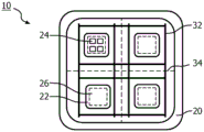
Fig. 1 is a cross-sectional view of a portion of a wafer prior to singulation, wherein the substrate has cavities, each containing one or more LED dies. The cavity is filled with a wavelength converting material and hermetically sealed by a flat transparent plate.
Fig. 2 is a top down view of a portion of the wafer of fig. 1 showing the seal around each cavity (the seal is shown greatly narrowed for ease of identification).
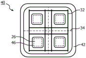
Fig. 3 is a simplified cross-sectional view of a portion of a wafer prior to singulation, wherein the substrate is substantially flat and supports LED dies, wherein a wavelength material is molded over each LED die to encapsulate the LED dies, wherein a transparent plate has cavities, and wherein a hermetic seal is formed around each cavity.
Fig. 4 is a top down view of a portion of the wafer of fig. 3 showing the seal around each plate cavity.
Fig. 5 is a cross-sectional view of a portion of a plate of a single singulated LED module having an optical pattern shaped for light emission. The optical pattern may form a lens, a light scattering feature, a reflector, a light absorber, or form any other feature.
FIG. 6 is a top down view of the plate portion of FIG. 5.
Fig. 7 is a cross-sectional view of a portion of a plate for a single singulated LED module illustrating a reflective ring formed around a single LED die area to concentrate light emission to a central area.
FIG. 8 is a top down view of the plate portion of FIG. 7.
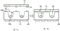
Fig. 9A and 9B are cross-sectional views of a portion of a wafer in which LED dies are mounted in cavities in a substrate and metal bonded using heat, such as with a low temperature AuSn solder, and in which the hermetic seal of the board is formed simultaneously using the same solder.
Fig. 10A illustrates how the cavities in the structure of fig. 9B are then filled with wavelength converting material through openings in the plate, so the wavelength converting material avoids the solder heating step of fig. 9B.
Fig. 10B illustrates how the opening in the plate is then filled to complete the hermetic seal.
Fig. 11 is a top down view of a portion of a board with a single singulated LED module forming a vertical column, multiple sealed cavities containing wavelength converting material.
Fig. 12 is a cross-sectional view of a single LED module after singulation using the plate of fig. 11, as viewed along line 12-12 in fig. 11, wherein the wavelength converting material fills the cavities in the plate, and wherein the plate is covered by an optional phosphor layer to generate additional wavelengths.
Fig. 13 is similar to fig. 11 except that the cavities in the plate are horizontal cylinders filled with wavelength material, sealed after singulation.
Fig. 14 is a cross-sectional view of an individual LED module after singulation using the plate of fig. 13, as viewed along line 14-14 in fig. 13, wherein the wavelength converting material fills the cavity, and wherein the plate is covered with an encapsulant (containing phosphor particles) to seal the ends of the cavity.
Fig. 15 is a top down view of a hollow strip made of ceramic or glass that has been filled with a wavelength converting material by capillary action. Alternatively, the daughter board may contain a horizontal cavity filled with a wavelength converting material.
Fig. 16 is a cross-sectional view of an individual LED module after singulation using the strip or sub-board of fig. 16, as viewed along line 16-16 in fig. 15, wherein the strip or sub-board is bonded to a top plate which is then bonded to a substrate having a cavity containing an LED die. The bonding creates a hermetic seal. The ends of the horizontal cavity are then hermetically sealed with an encapsulant, if desired.
The same or similar elements are labeled with the same reference numerals.
Detailed Description
Fig. 1 illustrates a portion of a wafer 10 prior to singulation. The wafer 10 includes a substrate 20 and a transparent plate 30. The substrate 20 is formed of a high thermal conductivity material. The substrate 20 may be formed, for example, of a transparent ceramic such as sapphire, spinel, or polycrystalline alumina. The substrate 20 may also be formed of any other transparent or non-transparent ceramic material, including molded ceramic materials in which ceramic powders are molded and sintered under pressure. In other embodiments, the substrate 20 may be a glass-ceramic. In another embodiment, the substrate 20 may be a metal lead frame enclosed in an elastomeric body.
In fig. 1, a substrate 20 is molded or machined to have a cavity 22. If the substrate 20 is formed of a light absorbing material, the cavity 22 walls may be coated with a reflective film (preferably at least 90% reflective for visible light). The substrate 20 may even be formed of a reflective material, such as a white ceramic material. In the alternative, the reflectivity of the film or substrate 20 may be for non-visible light, such as UV light.
The bottom of each cavity 22 has conventional electrodes (not shown) that are electrically connected to conventional bottom metal pads (not shown) on the substrate 20 for soldering the singulated LED modules to a Printed Circuit Board (PCB) or other substrate. The cavity electrodes are positioned to correspond to electrodes on the particular LED die 24 used (such as flip-chip LEDs, vertical LEDs, etc.). The substrate 20 may be molded to include vias and, using conventional techniques, metal is deposited and patterned to form various electrodes in the cavities 22, fill the vias, and form metal pads on the bottom surface of the substrate 20. The electrodes provide a thermally conductive path between the LED die 24 and the substrate 20. An electrically insulating metal thermal pad may also be located on the bottom of the LED die 24 and bonded to the metal thermal pad in the cavity 22.
If the substrate 20 has a top surface, such as a porous surface, that provides poor adhesion, a top layer, such as a sealant layer, may be deposited on the substrate 20 surface to achieve a better hermetic seal between the substrate 20 and a top plate (described below).
In one embodiment, the LED dies 24 are high brightness LED dies that emit blue light. Such LED dies 24 generate relatively high heat, and such heat needs to be spread and removed by the substrate 20 and the PCB to which the substrate 20 is later mounted via a conductive object. Heat conducted horizontally and then vertically upward through the substrate 20 is preferably not blocked by any overlying structures so that ambient air above the substrate 20 can also remove heat by conduction and/or convection.
In fig. 1, four LED dies 24 are mounted in each cavity 22 for additional brightness, but only two are shown per cavity 22 in cross-section.
The cavity 22 is then filled or partially filled with the wavelength converting material 26. Such material 26 will typically be a phosphor powder in a binder or quantum dots dispersed in a carrier. The support for the quantum dot will also be referred to as a binder. Quantum dots with submicron dimensions do not precipitate and remain fairly well dispersed in the binder. The transparent bonding material may be a polymer, such as silicone. Many types of phosphors and quantum dots degrade at high heat, so it is an object of the present invention to provide a structure that allows heat to be removed from the LED die while limiting heating of the wavelength conversion material.
The volume of each cavity 22 is much larger than the volume of each LED die 24. Thus, the volume of the wavelength converting material 26 is relatively high, enabling a low concentration of phosphor particles or quantum dots. The thermal conductivity of the wavelength converting material (including its binder) is several orders of magnitude lower than the thermal conductivity of the substrate 20 (e.g., 0.1-0.2W/mK versus 30W/mK). Thus, the bulk and low thermal conductivity of the wavelength converting material 26 limits the amount of heat conducted to the phosphor particles or quantum dots. In other words, the length of heat diffusion within material 26 is very small. Thus, the phosphor particles or quantum dots do not degrade significantly, even if high heat is generated by the LED die 24, if they are distributed throughout the wavelength conversion material 26.
Furthermore, if the quantum dots contain toxic elements such as cadmium, the RoHS directive (a limitation on the use of certain hazardous substances) requires dilution of the cadmium metal in the quantum dot film to meet compliance. This can be achieved by increasing the volume of the binder and decreasing the quantum dot concentration while still maintaining the desired color emission (such as the desired warm white point).
Any voids between the top of the wavelength converting material 26 and the top of the cavity 22 may be filled with a transparent binder material to avoid air pockets and concomitant reflective effects.
Next, a flat transparent ceramic, glass or elastomeric plate 30 is provided. Other materials may also be suitable. Plate 30 will be about the same wafer size as substrate 20. In one embodiment, the plate is about 100 microns thick to minimize light absorption and create a high thermal conductivity path to ambient air.
A transparent encapsulant material 32 is deposited, such as by screen printing, on the plate 30 and/or on the substrate 20 to surround each cavity 22. The encapsulant material 32 should have good thermal conductivity and cover a large area so that heat is conducted to the plate 30 and the ambient air. The sealant material 32 may be low temperature glass, glass paste, metal oxide, high thermal conductivity epoxy, or other suitable material that can form a hermetic seal. In one embodiment, the sealant material 32 is heated or cured by laser annealing, laser heating, furnace heating, or optical curing to create a hermetic seal. The sealant material 32 and other materials should be selected to have similar coefficients of thermal expansion to avoid delamination during operation.
The sealing process may be performed in a vacuum to remove air from the cavity 22, and a downward pressure may be applied to the plate 30.
The resulting wafer is then singulated along lines 34, such as by sawing, to form individual LED modules. The combination of the blue light and the light generated by the wavelength converting material 26 may create any color of light visually.
The combination of the substrate 20, encapsulant material 32, and plate 30, all of which are high thermal conductivity materials, removes heat from the LED die 24 by conducting the heat to ambient air and a thermally conductive printed circuit board (e.g., a circuit board with a metallic body), allowing most or all of the low thermal conductivity wavelength conversion material 26 to remain below 130 ℃, which is sufficient for most wavelength conversion materials to avoid degradation.
Because the encapsulant material 32 is remote from the high flux of blue light and the opaque reflective layer in the cavity 22 can block light impinging on the encapsulant material 32, the requirement for the encapsulant material 32 to withstand high flux is reduced.
Fig. 2 is a top down view of a portion of the wafer 10 of fig. 1 showing possible locations of the encapsulant material 32 around each cavity 22. The sealant material 32 is illustrated as a narrow "bead," which is not to scale for the exemplary embodiment in order to illustrate its location. In another embodiment, the entire surface of the plate 30 is coated with a sealant material 32 to increase thermal conductivity to the substrate 20.
Fig. 3 is a simplified cross-sectional view of a small portion of a wafer 40 prior to singulation, in which the substrate 42 is substantially flat and supports the LED dies 24. The LED die 24 has conventional metal electrodes (anode and cathode) electrically and thermally connected to corresponding electrodes on the substrate 42, as discussed with respect to fig. 1.
The substrate 42 (as a wafer) is brought against a mold having cavities filled with uncured wavelength converting material 26. The wavelength converting material 26 encapsulates the LED die 24. Material 26 is then cured and substrate 42 is released from the mold. Preferably, the resulting molded material 26 is relatively thick, with a low concentration of phosphor particles or quantum dots in a low thermal conductivity transparent binder, so that most or all of the phosphor particles or quantum dots are not subjected to high heat.
A transparent plate 44, such as formed of glass or ceramic, is molded, machined, etched, or otherwise formed to have a cavity 46. The plate 44 is sealed to the substrate 42 under vacuum by the sealant material 32, which sealant material 32 may be the same as described with respect to fig. 1 and cured in the same manner. Preferably, the amount of air should be minimized in the gap between the molded material 26 and the top of the cavity 46 to avoid delamination of the LED die 24 as heat is generated during operation. The wafer is then singulated along lines 34.
Due to the encapsulant material 32 used, the spread of the encapsulant material 32 over a large area, the distribution of heat and flux from the LED die 24, the high thermal conductivity of the substrate 42 and the plate 44, and the low conductivity and large volume of the wavelength converting material 26, the encapsulation is reliable at high heat and flux and the phosphor or quantum dots do not experience high heat.
In all embodiments, the high thermal conductivity material (including the substrate and the top plate) should have a conductivity greater than 20W/mK. Since the encapsulant material may be very thin, its thermal conductivity is not critical, although it is preferred to make it high.
The planar substrate 42 preferably has a reflective layer on its top surface, which may be specular or diffuse reflective, to reflect light upward. The reflective layer may be metal, white paint, or the like.
Fig. 4 is a top down view of a small portion of the wafer 40 of fig. 3 showing the location of the encapsulant material 32 around each plate cavity 46. The sealant material 32 is spread over a much larger area, as shown in fig. 3, but is illustrated as a narrow "seam" which is not to scale for the exemplary embodiment shown in fig. 4 to better illustrate the general location of the seal.
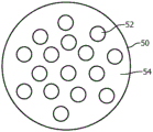
Fig. 5 is a cross-sectional view of a plate 50 for a single singulated LED module. The bottom of plate 50 is sealed to a substrate, such as shown in fig. 1 or 3. The bottom of the plate 50 may be flat or have a cavity. Fig. 5 illustrates that the plate 50 may include optical features 52 that may, for example, scatter or form lenses or redirect or absorb light or reflect light. In the simplified example of fig. 5 and 6, the optical feature 52 is a cylindrical depression.
Fig. 6 is a top down view of the plate 50 shown in fig. 5, with the optical features 52 shown as circular depressions in the plate 50. The plate 50 may also include a reflective film 54 over other areas so that most of the light is emitted almost exclusively through the circular depressions. By providing the plate 50 with a non-planar top surface, internal reflection is reduced. In another embodiment, the recesses are angled prisms to increase light extraction. The plate 50 is shown as circular, but may be rectangular or any other suitable shape.
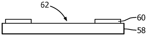
Fig. 7 is a cross-sectional view of a plate 58 for a single singulated LED module illustrating a reflective ring 60 formed around the single LED die area to limit light emission to a central area 62. The bottom of the plate 58 may be flat or have a cavity and is sealed to the substrate as described above. The ring 60 may be deposited aluminum, silver or other reflective material. The LED light rays impinging on the bottom surface of ring 60 are directed downward and reflected back upward from the reflective surface of a substrate, such as substrate 42 in fig. 3.
Fig. 8 is a top down view of the plate 58 of fig. 7 showing the reflective ring 60 and the transparent central region 62. The plate 58 may also be rectangular or any other suitable shape.
Fig. 9A and 9B are cross-sectional views of a portion of a wafer in which LED dies 24 are mounted in cavities 66 in a substrate 68 and metal bonded to the substrate electrode using heat, such as with a low temperature AuSn solder 70A, and in which a hermetic seal of a board 72 is formed simultaneously using the same solder 70B. The solder 70A bonding the LED die 24 to the substrate electrodes provides electrical conductivity to conventional anode and cathode base pads 71 on the substrate 68 and also provides thermal conductivity to the bulk of the substrate 68. It is also possible to provide large thermal pads that are electrically insulated. The plate 72 is provided with a metal ring 74 which is bonded to the solder 70B to form a hermetic seal with the substrate 68.
The solder 70B and metal ring 74 may be much wider than shown in fig. 9A and 9B to provide a wide seal with good thermal conductivity between the top plate 72 and the substrate 68.
Fig. 10A illustrates how the cavity 66 in the substrate 68 of fig. 9B is then substantially completely filled with the wavelength converting material 26 (to prevent air gaps) through the small opening 76 in the plate 72, so the wavelength converting material 26 avoids the solder 70 heating step of fig. 9B. The wavelength converting material 26 has a relatively large volume, has a low thermal conductivity, and has a low concentration of phosphor particles or quantum dots to limit the temperature of the phosphor particles or quantum dots. In an alternative embodiment, multiple openings 76 are used for each cavity 66 to allow air to escape as the wavelength conversion material 26 is introduced. Likewise, some of the openings 76 may be connected to a vacuum source to "draw" the conversion material 26 into the cavity 66.
Fig. 10B illustrates how the opening 76 in the plate 72 is then filled with another type of sealant material 78 (e.g., silicone or epoxy) to complete the hermetic seal.
The resulting wafer may then be singulated, such as through the middle of the structure of fig. 10B.
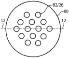
Fig. 11 is a top down view of a board 80 with a single singulated LED module forming a vertical column, containing multiple sealed cavities 82 of wavelength converting material 26.
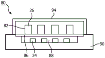
Fig. 12 is a cross-sectional view of a single LED module 84 after singulation using the board 80 of fig. 11, as viewed along line 12-12 in fig. 11. The wavelength converting material 26 is sealed in the cavity 82 by a transparent sealing plate 86, which transparent sealing plate 86 may also form a hermetic seal around a central cavity 88 in a substrate 90 in which the LED die 24 is mounted. Any of the sealant materials described above may be used around the periphery of the cavity 88. The plate 80 is optionally covered by a remote phosphor layer 94 to generate additional wavelengths. Since the various wavelength converting materials are remote from the LED die 24, the materials are not subject to high temperatures and do not degrade. If the hermetic seal of any one chamber 82 is broken, this does not affect the seal for the other chambers 82.
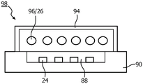
Fig. 13 is similar to fig. 11 except that the cavities 96 in the plate 98 are horizontal cylinders filled with the wavelength converting material 26. The cavity 96 extends all the way to the edge of the plate 98 and the open end of the cavity 96 is sealed by a suitable sealant material 100, such as silicone or epoxy. The cavity 96 may be filled by capillary action.
Fig. 14 is a cross-sectional view of a single LED module after singulation using the plate 98 of fig. 13, as viewed along line 14-14 in fig. 13. The plate 98 is mated with the same substrate 90 as described with respect to fig. 12. The periphery of plate 98 surrounding substrate cavity 88 includes a hermetic seal, as described above. The ends of the cavity 96 may be sealed by a silicone binder material in the optional phosphor layer 94 over the plate 98.
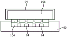
Fig. 15 is a top down view of a ceramic or glass hollow strip 104 that has been filled with wavelength converting material 26 by capillary action. Alternatively, the daughter board may contain a horizontal cavity filled with the wavelength converting material 26.
Fig. 16 is a cross-sectional view of an individual LED module after singulation using the strip 104 or sub-board of fig. 15, as viewed along line 16-16 in fig. 15, wherein the strip 104 or sub-board is bonded to a top plate 106, which top plate 106 is then sealed to the substrate 90 having the cavity 88 containing the LED die 24. If desired, the ends of the horizontal cavity 104 are hermetically sealed with a suitable sealant material 108 (FIG. 15). An optional phosphor layer 94 may be deposited over the plate 106.
In fig. 11-16, portions for a single LED module are shown. However, if the top plate is used to seal the module during the wafer-level process (before singulation), after singulation, the edges of the top plate and the substrate will coincide for the collection of LED modules, similar to fig. 1 and 3. This greatly reduces the cost of the LED module.
In all embodiments, the wavelength converting material 26 temperature remains relatively low, and the encapsulant material provides a reliable hermetic seal even though the LED die generates high heat and flux through a combination of the various factors described herein, even in the case of high brightness LED dies.
Preferably, in all embodiments, there is no air trapped in the cavity to avoid delamination when the LED module is heated by operation of the LED die. This can be done by completely filling the cavity or performing a hermetic sealing step in vacuum.
By sealing the top plate to the substrate as a wafer and then singulating the wafer, the edge of the top plate will typically coincide with the edge of the substrate. Forming a hermetic seal during the wafer process is much less expensive than sealing each module after singulation. Thus, the process described herein can be performed with little additional cost per LED module.
While particular embodiments of the present invention have been shown and described, it will be obvious to those skilled in the art that changes and modifications may be made without departing from this invention in its broader aspects and, therefore, the appended claims are to encompass within their scope all such changes and modifications as fall within the true spirit and scope of this invention.
Claims (13)
1. A light emitting device comprising:
a substrate having a first thermal conductivity;
a light emitting diode on the substrate;
a wavelength conversion material positioned overlying the light emitting diode, the wavelength conversion material comprising quantum dots dispersed in a binder, having a second thermal conductivity substantially lower than the first thermal conductivity, and having a total volume higher than the total volume of the light emitting diode;
a transparent plate disposed on the substrate and having a third thermal conductivity greater than the second thermal conductivity; and
a sealant forming a hermetic seal between the transparent plate and the substrate,
wherein the light emitting diode is located in a cavity in the substrate or in the transparent plate.
2. The light emitting device of claim 1 wherein the cavity is in the substrate.
3. The light emitting device of claim 1 wherein the cavity is in a transparent plate.
4. The light emitting device of claim 1, wherein the transparent plate comprises glass and the encapsulant comprises melted glass attaching the transparent plate to the substrate.
5. The light emitting device of claim 1, wherein the encapsulant comprises a metal solder material and the light emitting diode is bonded to the electrode on the substrate with a conductive bond formed from the same metal solder material.
6. The light emitting device of claim 1, wherein the transparent plate includes features that redirect light emitted by the light emitting diode or by the wavelength converting material.
7. The light emitting device of claim 1, wherein in operation, heat generated by the light emitting diode is at least partially removed by thermal conduction through the substrate, the encapsulant, and the transparent plate, and the temperature of the wavelength converting material is lower than the temperature of the light emitting diode.
8. The light emitting device of claim 1, wherein:
the transparent plate includes a flat sidewall edge around a perimeter of the transparent plate;
the substrate includes a flat sidewall edge around a perimeter of the substrate; and is
The flat sidewall edge of the transparent plate coincides with the flat sidewall edge of the substrate.
9. The light emitting device of claim 1, wherein the wavelength converting material fills the cavity.
10. The light emitting device of claim 1, wherein:
the cavity is positioned in the substrate; and is
In operation, heat generated by the light emitting diode is at least partially removed by thermal conduction through the substrate, encapsulant, and transparent plate, and the temperature of the wavelength converting material is lower than the temperature of the light emitting diode.
11. The light emitting device of claim 10 wherein the transparent plate includes an opening over the cavity.
12. The light emitting device of claim 11, wherein the opening is hermetically sealed.
13. The light emitting device of claim 11, wherein:
the transparent plate includes a flat sidewall edge around a perimeter of the transparent plate;
the substrate includes a flat sidewall edge around a perimeter of the substrate; and is
The flat sidewall edge of the transparent plate coincides with the flat sidewall edge of the substrate.
Applications Claiming Priority (3)
| Application Number | Priority Date | Filing Date | Title |
|---|---|---|---|
| US201361763081P | 2013-02-11 | 2013-02-11 | |
| US61/763081 | 2013-02-11 | ||
| CN201480008361.9A CN104969371A (en) | 2013-02-11 | 2014-02-10 | Led module with hermetic seal of wavelength conversion material |
Related Parent Applications (1)
| Application Number | Title | Priority Date | Filing Date |
|---|---|---|---|
| CN201480008361.9A Division CN104969371A (en) | 2013-02-11 | 2014-02-10 | Led module with hermetic seal of wavelength conversion material |
Publications (2)
| Publication Number | Publication Date |
|---|---|
| CN110010742A CN110010742A (en) | 2019-07-12 |
| CN110010742B true CN110010742B (en) | 2021-11-12 |
Family
ID=50151344
Family Applications (2)
| Application Number | Title | Priority Date | Filing Date |
|---|---|---|---|
| CN201910257207.XA Active CN110010742B (en) | 2013-02-11 | 2014-02-10 | Hermetically sealed LED module with wavelength conversion material |
| CN201480008361.9A Pending CN104969371A (en) | 2013-02-11 | 2014-02-10 | Led module with hermetic seal of wavelength conversion material |
Family Applications After (1)
| Application Number | Title | Priority Date | Filing Date |
|---|---|---|---|
| CN201480008361.9A Pending CN104969371A (en) | 2013-02-11 | 2014-02-10 | Led module with hermetic seal of wavelength conversion material |
Country Status (7)
| Country | Link |
|---|---|
| US (3) | US10002855B2 (en) |
| EP (1) | EP2954566B1 (en) |
| JP (2) | JP2016507162A (en) |
| KR (1) | KR20150119179A (en) |
| CN (2) | CN110010742B (en) |
| TW (1) | TWI645583B (en) |
| WO (1) | WO2014122626A1 (en) |
Families Citing this family (21)
| Publication number | Priority date | Publication date | Assignee | Title |
|---|---|---|---|---|
| KR102294837B1 (en) * | 2013-08-16 | 2021-08-26 | 삼성전자주식회사 | Methods for making optical components, optical components, and products including same |
| US10374137B2 (en) * | 2014-03-11 | 2019-08-06 | Osram Gmbh | Light converter assemblies with enhanced heat dissipation |
| DE102014108282A1 (en) * | 2014-06-12 | 2015-12-17 | Osram Opto Semiconductors Gmbh | Optoelectronic semiconductor component, method for producing an optoelectronic semiconductor component and light source with an optoelectronic semiconductor component |
| US9481572B2 (en) * | 2014-07-17 | 2016-11-01 | Texas Instruments Incorporated | Optical electronic device and method of fabrication |
| TW201624776A (en) * | 2014-12-18 | 2016-07-01 | Edison Opto Corp | LED lighting module |
| US20180301605A1 (en) * | 2015-03-19 | 2018-10-18 | Osram Opto Semiconductors Gmbh | A window that covers an optoelectronic semiconductor chip, a panel comprising a plurality of windows, a method of producing windows and an optoelectronic semiconductor device |
| CN107810565A (en) * | 2015-06-26 | 2018-03-16 | 康宁股份有限公司 | Sealing device and its manufacture method comprising quantum dot |
| DE102015111910A1 (en) * | 2015-07-22 | 2017-01-26 | Osram Opto Semiconductors Gmbh | Optoelectronic component, composite of optoelectronic components and method for producing an optoelectronic component |
| EP3334700A1 (en) * | 2015-08-12 | 2018-06-20 | Corning Incorporated | Sealed devices and methods for making the same |
| KR101778848B1 (en) * | 2015-08-21 | 2017-09-14 | 엘지전자 주식회사 | Light emitting device package assembly and method of fabricating the same |
| CN109314170B (en) * | 2015-12-02 | 2023-05-09 | 亮锐控股有限公司 | LED metal pad configuration for optimized thermal resistance, solder reliability and SMT process yield |
| US10211384B2 (en) | 2016-03-28 | 2019-02-19 | Samsung Electronics Co., Ltd. | Light emitting diode apparatus and manufacturing method thereof |
| JP6748501B2 (en) * | 2016-07-14 | 2020-09-02 | ローム株式会社 | Electronic component and manufacturing method thereof |
| KR102627073B1 (en) * | 2016-11-30 | 2024-01-19 | 삼성디스플레이 주식회사 | Backlight unit, display device and manufacturing method of display device |
| JP6790899B2 (en) | 2017-02-17 | 2020-11-25 | 日亜化学工業株式会社 | Light emitting module manufacturing method and light emitting module |
| DE102017109083A1 (en) * | 2017-04-27 | 2018-10-31 | Osram Gmbh | Lighting device and method for producing a lighting device |
| US20180323354A1 (en) * | 2017-05-07 | 2018-11-08 | Yang Wang | Light emitting device and method for manufacturing light emitting device |
| TWI658610B (en) * | 2017-09-08 | 2019-05-01 | Maven Optronics Co., Ltd. | Quantum-dot-based color-converted light emitting device and method for manufacturing the same |
| KR102415343B1 (en) * | 2017-09-25 | 2022-06-30 | 엘지전자 주식회사 | Display device |
| KR102498252B1 (en) * | 2017-09-26 | 2023-02-10 | 삼성전자주식회사 | Display including luminous chips and manufacturing method thereof |
| CN109962149B (en) * | 2017-12-14 | 2020-10-27 | Tcl科技集团股份有限公司 | Packaging film, preparation method thereof and photoelectric device |
Citations (3)
| Publication number | Priority date | Publication date | Assignee | Title |
|---|---|---|---|---|
| CN101449398A (en) * | 2006-03-30 | 2009-06-03 | 住友化学株式会社 | Light emitting element |
| WO2010078203A1 (en) * | 2008-12-31 | 2010-07-08 | Intematix Corporation | Light emitting device with phosphor wavelength conversion |
| JP2010177375A (en) * | 2009-01-28 | 2010-08-12 | Citizen Electronics Co Ltd | Light-emitting device and manufacturing method of the same |
Family Cites Families (32)
| Publication number | Priority date | Publication date | Assignee | Title |
|---|---|---|---|---|
| JP2003298115A (en) * | 2002-04-05 | 2003-10-17 | Citizen Electronics Co Ltd | Light emitting diode |
| JP2004047748A (en) * | 2002-07-12 | 2004-02-12 | Stanley Electric Co Ltd | Light-emitting diode |
| US7824937B2 (en) * | 2003-03-10 | 2010-11-02 | Toyoda Gosei Co., Ltd. | Solid element device and method for manufacturing the same |
| US7087465B2 (en) | 2003-12-15 | 2006-08-08 | Philips Lumileds Lighting Company, Llc | Method of packaging a semiconductor light emitting device |
| US8816369B2 (en) * | 2004-10-29 | 2014-08-26 | Led Engin, Inc. | LED packages with mushroom shaped lenses and methods of manufacturing LED light-emitting devices |
| JP5113329B2 (en) | 2005-11-25 | 2013-01-09 | パナソニック株式会社 | Light emitting device |
| JP4881001B2 (en) * | 2005-12-29 | 2012-02-22 | シチズン電子株式会社 | Light emitting device |
| JP2007243052A (en) * | 2006-03-10 | 2007-09-20 | Matsushita Electric Works Ltd | Lighting fixture and its manufacturing method |
| JP2007250817A (en) | 2006-03-16 | 2007-09-27 | Stanley Electric Co Ltd | Led |
| US20080029774A1 (en) * | 2006-08-04 | 2008-02-07 | Acol Technologies S.A. | Semiconductor light source packages with broadband and angular uniformity support |
| US20080203412A1 (en) * | 2007-02-28 | 2008-08-28 | E-Pin Optical Industry Co., Ltd. | LED assembly with molded glass lens |
| KR101686669B1 (en) | 2007-03-19 | 2016-12-14 | 나노시스, 인크. | Methods for encapsulating nanocrystals |
| GB0801509D0 (en) * | 2008-01-28 | 2008-03-05 | Photonstar Led Ltd | Light emitting system with optically transparent thermally conductive element |
| US7855394B2 (en) | 2009-06-18 | 2010-12-21 | Bridgelux, Inc. | LED array package covered with a highly thermal conductive plate |
| CN102110756B (en) * | 2009-12-23 | 2012-10-03 | 海洋王照明科技股份有限公司 | White light LED (light-emitting diode) and packaging method thereof |
| JP5497469B2 (en) * | 2010-02-16 | 2014-05-21 | スタンレー電気株式会社 | Light emitting device and manufacturing method thereof |
| KR20110094996A (en) * | 2010-02-18 | 2011-08-24 | 엘지이노텍 주식회사 | Package of light emitting device and method for fabricating the same and lighting system including the same |
| JP2011192845A (en) * | 2010-03-15 | 2011-09-29 | Seiko Instruments Inc | Light-emitting component, light-emitting device, and method of manufacturing light-emitting component |
| JP2011216712A (en) * | 2010-03-31 | 2011-10-27 | Citizen Finetech Miyota Co Ltd | Electronic device |
| US8723409B2 (en) * | 2010-04-07 | 2014-05-13 | Nichia Corporation | Light emitting device |
| JP2011249729A (en) | 2010-05-31 | 2011-12-08 | Hitachi Kyowa Engineering Co Ltd | Optical element mounting substrate and optical element mounting package |
| US20110317397A1 (en) | 2010-06-23 | 2011-12-29 | Soraa, Inc. | Quantum dot wavelength conversion for hermetically sealed optical devices |
| US8624491B2 (en) * | 2010-07-22 | 2014-01-07 | Kyocera Corporation | Light emitting device |
| CN102347420A (en) * | 2010-08-04 | 2012-02-08 | 展晶科技(深圳)有限公司 | Light emitting diode (LED) manufacturing method |
| TWI406435B (en) | 2010-08-06 | 2013-08-21 | Advanced Optoelectronic Tech | Method for manufacturing led |
| US8198109B2 (en) | 2010-08-27 | 2012-06-12 | Quarkstar Llc | Manufacturing methods for solid state light sheet or strip with LEDs connected in series for general illumination |
| JP2012134435A (en) | 2010-11-30 | 2012-07-12 | Mitsubishi Shindoh Co Ltd | Light-emitting device for back light |
| US8253330B2 (en) * | 2010-11-30 | 2012-08-28 | GEM Weltronics TWN Corporation | Airtight multi-layer array type LED |
| JP2012156409A (en) | 2011-01-28 | 2012-08-16 | Mitsubishi Shindoh Co Ltd | Light-emitting device for backlight |
| US20120261703A1 (en) * | 2011-03-21 | 2012-10-18 | Zimmerman Scott M | Self-cooling solid-state emitters |
| WO2013001687A1 (en) * | 2011-06-30 | 2013-01-03 | パナソニック株式会社 | Light-emitting device |
| US20140299902A1 (en) * | 2012-01-18 | 2014-10-09 | Goldeneye, Inc. | Articles and methods for rapid manufacturing of solid state light sources |
-
2014
- 2014-02-10 JP JP2015556606A patent/JP2016507162A/en not_active Ceased
- 2014-02-10 WO PCT/IB2014/058875 patent/WO2014122626A1/en active Application Filing
- 2014-02-10 CN CN201910257207.XA patent/CN110010742B/en active Active
- 2014-02-10 KR KR1020157024839A patent/KR20150119179A/en not_active IP Right Cessation
- 2014-02-10 US US14/762,576 patent/US10002855B2/en active Active
- 2014-02-10 EP EP14705885.3A patent/EP2954566B1/en active Active
- 2014-02-10 CN CN201480008361.9A patent/CN104969371A/en active Pending
- 2014-02-11 TW TW103104452A patent/TWI645583B/en active
-
2018
- 2018-06-14 US US16/008,131 patent/US10700044B2/en active Active
-
2019
- 2019-10-03 JP JP2019182604A patent/JP2019220726A/en active Pending
-
2020
- 2020-06-29 US US16/915,497 patent/US11081471B2/en active Active
Patent Citations (3)
| Publication number | Priority date | Publication date | Assignee | Title |
|---|---|---|---|---|
| CN101449398A (en) * | 2006-03-30 | 2009-06-03 | 住友化学株式会社 | Light emitting element |
| WO2010078203A1 (en) * | 2008-12-31 | 2010-07-08 | Intematix Corporation | Light emitting device with phosphor wavelength conversion |
| JP2010177375A (en) * | 2009-01-28 | 2010-08-12 | Citizen Electronics Co Ltd | Light-emitting device and manufacturing method of the same |
Also Published As
| Publication number | Publication date |
|---|---|
| KR20150119179A (en) | 2015-10-23 |
| US20200328194A1 (en) | 2020-10-15 |
| JP2019220726A (en) | 2019-12-26 |
| US20180366451A1 (en) | 2018-12-20 |
| TW201442294A (en) | 2014-11-01 |
| US11081471B2 (en) | 2021-08-03 |
| WO2014122626A1 (en) | 2014-08-14 |
| CN110010742A (en) | 2019-07-12 |
| EP2954566A1 (en) | 2015-12-16 |
| JP2016507162A (en) | 2016-03-07 |
| EP2954566B1 (en) | 2020-04-08 |
| TWI645583B (en) | 2018-12-21 |
| US10002855B2 (en) | 2018-06-19 |
| CN104969371A (en) | 2015-10-07 |
| US10700044B2 (en) | 2020-06-30 |
| US20150371975A1 (en) | 2015-12-24 |
Similar Documents
| Publication | Publication Date | Title |
|---|---|---|
| US11081471B2 (en) | LED module with hermetic seal of wavelength conversion material | |
| JP6599295B2 (en) | LIGHT EMITTING ELEMENT HAVING BELT ANGLE REFLECTOR AND MANUFACTURING METHOD | |
| US10429011B2 (en) | Method of manufacturing light emitting device | |
| KR101847938B1 (en) | Light emitting device package and manufacturing method thereof | |
| WO2010123059A1 (en) | Method for manufacturing led light emitting device | |
| JP5569389B2 (en) | LIGHT EMITTING DEVICE MANUFACTURING METHOD AND LIGHT EMITTING DEVICE | |
| TW200931688A (en) | Resin-sealed light emitting device and its manufacturing method | |
| JP2008060542A (en) | Light-emitting device, method of manufacturing same, and light source device provided with the same | |
| EP3193379B1 (en) | Packaging for light emitting device and manufacturing method of the same | |
| TW201931625A (en) | System and method for chip-on-board light emitting diode | |
| EP2713411B1 (en) | Luminescence device | |
| EP2953172A1 (en) | Led light source package structure and led light source packaging method | |
| TWI565101B (en) | Light emitting diode package and method for forming the same | |
| US10910515B2 (en) | Method of manufacturing a light-emitting device | |
| JP7256372B2 (en) | Method for manufacturing light emitting device | |
| JPWO2015194296A1 (en) | Light emitting device | |
| TW202324793A (en) | Integrated warning structures for energized ultraviolet light-emitting diode packages | |
| KR20130091102A (en) | Led package and manufacturing method for the same |
Legal Events
| Date | Code | Title | Description |
|---|---|---|---|
| PB01 | Publication | ||
| PB01 | Publication | ||
| SE01 | Entry into force of request for substantive examination | ||
| SE01 | Entry into force of request for substantive examination | ||
| GR01 | Patent grant | ||
| GR01 | Patent grant |