KR20150110691A - 자기저항 터널 정션(mtj) 디바이스 강자성 층들에서 주변 엣지 손상을 개선시키기 위한 방법 및 장치 - Google Patents
자기저항 터널 정션(mtj) 디바이스 강자성 층들에서 주변 엣지 손상을 개선시키기 위한 방법 및 장치 Download PDFInfo
- Publication number
- KR20150110691A KR20150110691A KR1020157022599A KR20157022599A KR20150110691A KR 20150110691 A KR20150110691 A KR 20150110691A KR 1020157022599 A KR1020157022599 A KR 1020157022599A KR 20157022599 A KR20157022599 A KR 20157022599A KR 20150110691 A KR20150110691 A KR 20150110691A
- Authority
- KR
- South Korea
- Prior art keywords
- layer
- ferromagnetic
- tunnel junction
- forming
- magnetic tunnel
- Prior art date
- Legal status (The legal status is an assumption and is not a legal conclusion. Google has not performed a legal analysis and makes no representation as to the accuracy of the status listed.)
- Withdrawn
Links
- 238000000034 method Methods 0.000 title claims abstract description 307
- 230000005294 ferromagnetic effect Effects 0.000 title claims abstract description 287
- 230000002093 peripheral effect Effects 0.000 title claims abstract description 211
- 230000005291 magnetic effect Effects 0.000 claims abstract description 83
- 230000001131 transforming effect Effects 0.000 claims abstract description 30
- 239000010410 layer Substances 0.000 claims description 457
- 239000000945 filler Substances 0.000 claims description 57
- 239000011241 protective layer Substances 0.000 claims description 40
- 239000000758 substrate Substances 0.000 claims description 29
- 230000004888 barrier function Effects 0.000 claims description 22
- 238000005530 etching Methods 0.000 claims description 17
- 238000000992 sputter etching Methods 0.000 claims description 11
- 229910003321 CoFe Inorganic materials 0.000 claims description 9
- 229910019236 CoFeB Inorganic materials 0.000 claims description 9
- 239000004065 semiconductor Substances 0.000 claims description 9
- 229910019239 CoFx Inorganic materials 0.000 claims description 8
- 229910018874 CoNx Inorganic materials 0.000 claims description 8
- 229910002451 CoOx Inorganic materials 0.000 claims description 8
- 229910015471 FeFx Inorganic materials 0.000 claims description 8
- 229910015183 FeNx Inorganic materials 0.000 claims description 8
- 229910015189 FeOx Inorganic materials 0.000 claims description 8
- XEEYBQQBJWHFJM-UHFFFAOYSA-N Iron Chemical group [Fe] XEEYBQQBJWHFJM-UHFFFAOYSA-N 0.000 claims description 7
- 150000004767 nitrides Chemical class 0.000 claims description 7
- 229910017107 AlOx Inorganic materials 0.000 claims description 6
- 238000004891 communication Methods 0.000 claims description 6
- 238000012545 processing Methods 0.000 claims description 6
- PXHVJJICTQNCMI-UHFFFAOYSA-N Nickel Chemical compound [Ni] PXHVJJICTQNCMI-UHFFFAOYSA-N 0.000 claims description 5
- 238000005121 nitriding Methods 0.000 claims description 5
- 229910001030 Iron–nickel alloy Inorganic materials 0.000 claims description 4
- 230000001590 oxidative effect Effects 0.000 claims description 3
- 229910017052 cobalt Inorganic materials 0.000 claims description 2
- 239000010941 cobalt Substances 0.000 claims description 2
- GUTLYIVDDKVIGB-UHFFFAOYSA-N cobalt atom Chemical compound [Co] GUTLYIVDDKVIGB-UHFFFAOYSA-N 0.000 claims description 2
- 229910052759 nickel Inorganic materials 0.000 claims description 2
- 229910052742 iron Inorganic materials 0.000 claims 1
- 230000003647 oxidation Effects 0.000 abstract description 28
- 238000007254 oxidation reaction Methods 0.000 abstract description 28
- 238000003682 fluorination reaction Methods 0.000 abstract description 19
- 230000008569 process Effects 0.000 description 82
- 230000009466 transformation Effects 0.000 description 27
- 239000000126 substance Substances 0.000 description 21
- 238000004519 manufacturing process Methods 0.000 description 15
- 239000000463 material Substances 0.000 description 11
- 239000000203 mixture Substances 0.000 description 10
- 230000008901 benefit Effects 0.000 description 9
- 230000015572 biosynthetic process Effects 0.000 description 6
- 150000001875 compounds Chemical class 0.000 description 6
- 239000000470 constituent Substances 0.000 description 6
- 230000006870 function Effects 0.000 description 6
- 230000005415 magnetization Effects 0.000 description 6
- 238000003860 storage Methods 0.000 description 6
- 238000006243 chemical reaction Methods 0.000 description 4
- 238000005229 chemical vapour deposition Methods 0.000 description 4
- 238000010586 diagram Methods 0.000 description 4
- 230000000694 effects Effects 0.000 description 4
- -1 NiFeOx Inorganic materials 0.000 description 3
- 238000002161 passivation Methods 0.000 description 3
- 238000000844 transformation Methods 0.000 description 3
- 230000007704 transition Effects 0.000 description 3
- IJGRMHOSHXDMSA-UHFFFAOYSA-N Atomic nitrogen Chemical compound N#N IJGRMHOSHXDMSA-UHFFFAOYSA-N 0.000 description 2
- ZOXJGFHDIHLPTG-UHFFFAOYSA-N Boron Chemical compound [B] ZOXJGFHDIHLPTG-UHFFFAOYSA-N 0.000 description 2
- 239000013256 coordination polymer Substances 0.000 description 2
- 239000013078 crystal Substances 0.000 description 2
- 230000006735 deficit Effects 0.000 description 2
- 238000013461 design Methods 0.000 description 2
- 230000008030 elimination Effects 0.000 description 2
- 238000003379 elimination reaction Methods 0.000 description 2
- 238000005516 engineering process Methods 0.000 description 2
- 239000003302 ferromagnetic material Substances 0.000 description 2
- 238000004334 fluoridation Methods 0.000 description 2
- 230000005012 migration Effects 0.000 description 2
- 238000013508 migration Methods 0.000 description 2
- 229910052757 nitrogen Inorganic materials 0.000 description 2
- 229910052760 oxygen Inorganic materials 0.000 description 2
- 239000000047 product Substances 0.000 description 2
- 208000019585 progressive encephalomyelitis with rigidity and myoclonus Diseases 0.000 description 2
- 239000011253 protective coating Substances 0.000 description 2
- 230000009467 reduction Effects 0.000 description 2
- 235000012431 wafers Nutrition 0.000 description 2
- KRHYYFGTRYWZRS-UHFFFAOYSA-M Fluoride anion Chemical compound [F-] KRHYYFGTRYWZRS-UHFFFAOYSA-M 0.000 description 1
- QVGXLLKOCUKJST-UHFFFAOYSA-N atomic oxygen Chemical compound [O] QVGXLLKOCUKJST-UHFFFAOYSA-N 0.000 description 1
- 229910052796 boron Inorganic materials 0.000 description 1
- 230000015556 catabolic process Effects 0.000 description 1
- 238000012512 characterization method Methods 0.000 description 1
- 239000003795 chemical substances by application Substances 0.000 description 1
- 238000010276 construction Methods 0.000 description 1
- 238000007796 conventional method Methods 0.000 description 1
- 230000008878 coupling Effects 0.000 description 1
- 238000010168 coupling process Methods 0.000 description 1
- 238000005859 coupling reaction Methods 0.000 description 1
- 238000006731 degradation reaction Methods 0.000 description 1
- 230000001419 dependent effect Effects 0.000 description 1
- 238000000151 deposition Methods 0.000 description 1
- 230000006866 deterioration Effects 0.000 description 1
- 238000009792 diffusion process Methods 0.000 description 1
- 238000002845 discoloration Methods 0.000 description 1
- 238000009826 distribution Methods 0.000 description 1
- 230000002452 interceptive effect Effects 0.000 description 1
- 239000000696 magnetic material Substances 0.000 description 1
- 230000007246 mechanism Effects 0.000 description 1
- 229910044991 metal oxide Inorganic materials 0.000 description 1
- 150000004706 metal oxides Chemical class 0.000 description 1
- 238000012986 modification Methods 0.000 description 1
- 230000004048 modification Effects 0.000 description 1
- 239000001301 oxygen Substances 0.000 description 1
- 239000002245 particle Substances 0.000 description 1
- 239000002243 precursor Substances 0.000 description 1
- 238000011084 recovery Methods 0.000 description 1
- 230000008439 repair process Effects 0.000 description 1
- 239000013589 supplement Substances 0.000 description 1
- 238000012360 testing method Methods 0.000 description 1
- 238000009966 trimming Methods 0.000 description 1
Images


Classifications
-
- H01L43/08—
-
- G—PHYSICS
- G11—INFORMATION STORAGE
- G11C—STATIC STORES
- G11C11/00—Digital stores characterised by the use of particular electric or magnetic storage elements; Storage elements therefor
- G11C11/02—Digital stores characterised by the use of particular electric or magnetic storage elements; Storage elements therefor using magnetic elements
- G11C11/14—Digital stores characterised by the use of particular electric or magnetic storage elements; Storage elements therefor using magnetic elements using thin-film elements
- G11C11/15—Digital stores characterised by the use of particular electric or magnetic storage elements; Storage elements therefor using magnetic elements using thin-film elements using multiple magnetic layers
-
- G—PHYSICS
- G11—INFORMATION STORAGE
- G11C—STATIC STORES
- G11C11/00—Digital stores characterised by the use of particular electric or magnetic storage elements; Storage elements therefor
- G11C11/02—Digital stores characterised by the use of particular electric or magnetic storage elements; Storage elements therefor using magnetic elements
- G11C11/14—Digital stores characterised by the use of particular electric or magnetic storage elements; Storage elements therefor using magnetic elements using thin-film elements
- G11C11/155—Digital stores characterised by the use of particular electric or magnetic storage elements; Storage elements therefor using magnetic elements using thin-film elements with cylindrical configuration
-
- G—PHYSICS
- G11—INFORMATION STORAGE
- G11C—STATIC STORES
- G11C11/00—Digital stores characterised by the use of particular electric or magnetic storage elements; Storage elements therefor
- G11C11/02—Digital stores characterised by the use of particular electric or magnetic storage elements; Storage elements therefor using magnetic elements
- G11C11/16—Digital stores characterised by the use of particular electric or magnetic storage elements; Storage elements therefor using magnetic elements using elements in which the storage effect is based on magnetic spin effect
- G11C11/161—Digital stores characterised by the use of particular electric or magnetic storage elements; Storage elements therefor using magnetic elements using elements in which the storage effect is based on magnetic spin effect details concerning the memory cell structure, e.g. the layers of the ferromagnetic memory cell
-
- H01L43/10—
-
- H01L43/12—
-
- H01L43/14—
-
- H—ELECTRICITY
- H10—SEMICONDUCTOR DEVICES; ELECTRIC SOLID-STATE DEVICES NOT OTHERWISE PROVIDED FOR
- H10N—ELECTRIC SOLID-STATE DEVICES NOT OTHERWISE PROVIDED FOR
- H10N50/00—Galvanomagnetic devices
- H10N50/01—Manufacture or treatment
-
- H—ELECTRICITY
- H10—SEMICONDUCTOR DEVICES; ELECTRIC SOLID-STATE DEVICES NOT OTHERWISE PROVIDED FOR
- H10N—ELECTRIC SOLID-STATE DEVICES NOT OTHERWISE PROVIDED FOR
- H10N50/00—Galvanomagnetic devices
- H10N50/10—Magnetoresistive devices
-
- H—ELECTRICITY
- H10—SEMICONDUCTOR DEVICES; ELECTRIC SOLID-STATE DEVICES NOT OTHERWISE PROVIDED FOR
- H10N—ELECTRIC SOLID-STATE DEVICES NOT OTHERWISE PROVIDED FOR
- H10N50/00—Galvanomagnetic devices
- H10N50/80—Constructional details
-
- H—ELECTRICITY
- H10—SEMICONDUCTOR DEVICES; ELECTRIC SOLID-STATE DEVICES NOT OTHERWISE PROVIDED FOR
- H10N—ELECTRIC SOLID-STATE DEVICES NOT OTHERWISE PROVIDED FOR
- H10N50/00—Galvanomagnetic devices
- H10N50/80—Constructional details
- H10N50/85—Materials of the active region
Landscapes
- Engineering & Computer Science (AREA)
- Computer Hardware Design (AREA)
- Manufacturing & Machinery (AREA)
- Hall/Mr Elements (AREA)
- Mram Or Spin Memory Techniques (AREA)
Applications Claiming Priority (3)
| Application Number | Priority Date | Filing Date | Title |
|---|---|---|---|
| US13/749,731 | 2013-01-25 | ||
| US13/749,731 US20140210021A1 (en) | 2013-01-25 | 2013-01-25 | Method and apparatus for ameliorating peripheral edge damage in magnetoresistive tunnel junction (mtj) device ferromagnetic layers |
| PCT/US2014/012602 WO2014116742A1 (en) | 2013-01-25 | 2014-01-22 | Method and apparatus for ameliorating peripheral edge damage in magnetoresistive tunnel junction (mtj) device ferromagnetic layers |
Publications (1)
| Publication Number | Publication Date |
|---|---|
| KR20150110691A true KR20150110691A (ko) | 2015-10-02 |
Family
ID=50064802
Family Applications (1)
| Application Number | Title | Priority Date | Filing Date |
|---|---|---|---|
| KR1020157022599A Withdrawn KR20150110691A (ko) | 2013-01-25 | 2014-01-22 | 자기저항 터널 정션(mtj) 디바이스 강자성 층들에서 주변 엣지 손상을 개선시키기 위한 방법 및 장치 |
Country Status (6)
Cited By (1)
| Publication number | Priority date | Publication date | Assignee | Title |
|---|---|---|---|---|
| WO2020131206A1 (en) * | 2018-12-21 | 2020-06-25 | Applied Materials, Inc. | Methods for forming structures for mram applications |
Families Citing this family (13)
| Publication number | Priority date | Publication date | Assignee | Title |
|---|---|---|---|---|
| US9396781B2 (en) * | 2010-12-10 | 2016-07-19 | Avalanche Technology, Inc. | Magnetic random access memory having perpendicular composite reference layer |
| KR102175471B1 (ko) * | 2014-04-04 | 2020-11-06 | 삼성전자주식회사 | 자기 저항 메모리 장치 및 그 제조 방법 |
| KR102240769B1 (ko) * | 2014-08-14 | 2021-04-16 | 삼성전자주식회사 | 자기 메모리 장치 및 그의 형성방법 |
| US10170690B2 (en) | 2015-11-16 | 2019-01-01 | Samsung Electronics Co., Ltd. | Hybrid-fl with edge-modified coupling |
| CN108242504A (zh) * | 2016-12-27 | 2018-07-03 | 上海磁宇信息科技有限公司 | 一种磁性隧道结的修剪方法及其制备方法 |
| EP3343655B1 (en) * | 2016-12-29 | 2022-03-02 | IMEC vzw | Magnetic tunnel junction device |
| US10297746B2 (en) * | 2017-04-05 | 2019-05-21 | Taiwan Semiconductor Manufacturing Company, Ltd. | Post treatment to reduce shunting devices for physical etching process |
| CN117425353A (zh) | 2019-05-09 | 2024-01-19 | 联华电子股份有限公司 | 磁阻式随机存取存储器 |
| US11495737B2 (en) * | 2020-06-29 | 2022-11-08 | United Microelectronics Corp. | Magnetic tunnel junction (MTJ) device |
| CN114156404A (zh) * | 2021-11-09 | 2022-03-08 | 中电海康集团有限公司 | 一种具有高翻转效率的磁隧道结及其制备方法 |
| US20230189657A1 (en) * | 2021-12-09 | 2023-06-15 | Taiwan Semiconductor Manufacturing Co., Ltd. | Magnetic Tunnel Junction Device and Method of Forming the Same |
| US20230309415A1 (en) * | 2022-03-23 | 2023-09-28 | Tdk Corporation | Magneto resistive element |
| CN116106801B (zh) * | 2023-04-14 | 2023-06-20 | 珠海多创科技有限公司 | 磁阻传感器、磁传感装置及其制备方法 |
Family Cites Families (8)
| Publication number | Priority date | Publication date | Assignee | Title |
|---|---|---|---|---|
| US6365419B1 (en) * | 2000-08-28 | 2002-04-02 | Motorola, Inc. | High density MRAM cell array |
| US20030231437A1 (en) * | 2002-06-17 | 2003-12-18 | Childress Jeffrey R. | Current-perpendicular-to-plane magnetoresistive device with oxidized free layer side regions and method for its fabrication |
| JP2004146687A (ja) * | 2002-10-25 | 2004-05-20 | Toshiba Corp | 磁気記憶装置及びその製造方法 |
| TWI413117B (zh) * | 2005-09-13 | 2013-10-21 | Canon Anelva Corp | 磁阻效果元件之製造方法及製造裝置 |
| JP2008186506A (ja) * | 2007-01-29 | 2008-08-14 | Hitachi Global Storage Technologies Netherlands Bv | 薄膜磁気ヘッド及びその製造方法 |
| US8981502B2 (en) * | 2010-03-29 | 2015-03-17 | Qualcomm Incorporated | Fabricating a magnetic tunnel junction storage element |
| JP5214691B2 (ja) * | 2010-09-17 | 2013-06-19 | 株式会社東芝 | 磁気メモリ及びその製造方法 |
| JP5417367B2 (ja) * | 2011-03-22 | 2014-02-12 | 株式会社東芝 | 磁気メモリの製造方法 |
-
2013
- 2013-01-25 US US13/749,731 patent/US20140210021A1/en not_active Abandoned
-
2014
- 2014-01-22 CN CN201480005496.XA patent/CN105308684B/zh not_active Expired - Fee Related
- 2014-01-22 WO PCT/US2014/012602 patent/WO2014116742A1/en active Application Filing
- 2014-01-22 KR KR1020157022599A patent/KR20150110691A/ko not_active Withdrawn
- 2014-01-22 EP EP14703017.5A patent/EP2948953A1/en not_active Withdrawn
- 2014-01-22 JP JP2015555245A patent/JP2016505220A/ja not_active Ceased
-
2016
- 2016-05-09 US US15/149,396 patent/US20160254443A1/en not_active Abandoned
Cited By (2)
| Publication number | Priority date | Publication date | Assignee | Title |
|---|---|---|---|---|
| WO2020131206A1 (en) * | 2018-12-21 | 2020-06-25 | Applied Materials, Inc. | Methods for forming structures for mram applications |
| JP2022513995A (ja) * | 2018-12-21 | 2022-02-09 | アプライド マテリアルズ インコーポレイテッド | Mram用途のための構造を形成する方法 |
Also Published As
| Publication number | Publication date |
|---|---|
| CN105308684A (zh) | 2016-02-03 |
| JP2016505220A (ja) | 2016-02-18 |
| WO2014116742A1 (en) | 2014-07-31 |
| CN105308684B (zh) | 2019-05-07 |
| US20160254443A1 (en) | 2016-09-01 |
| US20140210021A1 (en) | 2014-07-31 |
| EP2948953A1 (en) | 2015-12-02 |
Similar Documents
| Publication | Publication Date | Title |
|---|---|---|
| KR20150110691A (ko) | 자기저항 터널 정션(mtj) 디바이스 강자성 층들에서 주변 엣지 손상을 개선시키기 위한 방법 및 장치 | |
| US11925122B2 (en) | Magnetoresistive structure having two dielectric layers, and method of manufacturing same | |
| US10103319B2 (en) | Ultrathin perpendicular pinned layer structure for magnetic tunneling junction devices | |
| KR101679724B1 (ko) | 스핀전달 토크 스위칭 디바이스들에서 스위칭 전류의 변형 유도 감소 | |
| US9548446B2 (en) | Synthetic antiferromagnet (SAF) coupled free layer for perpendicular magnetic tunnel junction (P-MTJ) | |
| CN104737317B (zh) | 制造基于磁电阻的器件的方法 | |
| US9595666B2 (en) | Method of fabricating smooth seed layers with uniform crystalline texture for high perpendicular magnetic anisotropy materials | |
| KR20160113048A (ko) | 수직 자기 이방성의 강화를 위한 이중 MgO 인터페이스 및 CoFeB 층을 갖는 수직 스핀 전달 토크(STT) 메모리 셀 | |
| EP2553742A1 (en) | Magnetic tunnel junction storage element and method of fabricating the same | |
| KR20160018688A (ko) | 메모리 셀들, 동작 및 제작의 방법들, 반도체 디바이스 구조들, 및 메모리 시스템들 | |
| CN108232002B (zh) | 一种制备磁性隧道结阵列的方法 | |
| US20140190933A1 (en) | Method of manufacturing a magnetoresistive device | |
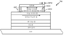
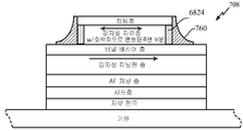
| US20140203381A1 (en) | Process and apparatus for transforming nitridation/oxidation at edges, and protecting edges of magnetoresistive tunnel junction (mtj) layers | |
| KR20040083934A (ko) | 마그네틱 램의 형성방법 | |
| CN108242504A (zh) | 一种磁性隧道结的修剪方法及其制备方法 | |
| CN107958952B (zh) | 一种半导体器件及其制造方法 | |
| KR20160012354A (ko) | Tddb를 방지하는 mtj 셀 및 그 제작 방법 |
Legal Events
| Date | Code | Title | Description |
|---|---|---|---|
| PA0105 | International application |
Patent event date: 20150820 Patent event code: PA01051R01D Comment text: International Patent Application |
|
| PG1501 | Laying open of application | ||
| PC1203 | Withdrawal of no request for examination | ||
| WITN | Application deemed withdrawn, e.g. because no request for examination was filed or no examination fee was paid |