KR20150110691A - Method and apparatus for ameliorating peripheral edge damage in magnetoresistive tunnel junction (mtj) device ferromagnetic layers - Google Patents
Method and apparatus for ameliorating peripheral edge damage in magnetoresistive tunnel junction (mtj) device ferromagnetic layers Download PDFInfo
- Publication number
- KR20150110691A KR20150110691A KR1020157022599A KR20157022599A KR20150110691A KR 20150110691 A KR20150110691 A KR 20150110691A KR 1020157022599 A KR1020157022599 A KR 1020157022599A KR 20157022599 A KR20157022599 A KR 20157022599A KR 20150110691 A KR20150110691 A KR 20150110691A
- Authority
- KR
- South Korea
- Prior art keywords
- layer
- ferromagnetic
- tunnel junction
- forming
- magnetic tunnel
- Prior art date
Links
Images


Classifications
-
- H01L43/08—
-
- G—PHYSICS
- G11—INFORMATION STORAGE
- G11C—STATIC STORES
- G11C11/00—Digital stores characterised by the use of particular electric or magnetic storage elements; Storage elements therefor
- G11C11/02—Digital stores characterised by the use of particular electric or magnetic storage elements; Storage elements therefor using magnetic elements
- G11C11/14—Digital stores characterised by the use of particular electric or magnetic storage elements; Storage elements therefor using magnetic elements using thin-film elements
- G11C11/15—Digital stores characterised by the use of particular electric or magnetic storage elements; Storage elements therefor using magnetic elements using thin-film elements using multiple magnetic layers
-
- G—PHYSICS
- G11—INFORMATION STORAGE
- G11C—STATIC STORES
- G11C11/00—Digital stores characterised by the use of particular electric or magnetic storage elements; Storage elements therefor
- G11C11/02—Digital stores characterised by the use of particular electric or magnetic storage elements; Storage elements therefor using magnetic elements
- G11C11/14—Digital stores characterised by the use of particular electric or magnetic storage elements; Storage elements therefor using magnetic elements using thin-film elements
- G11C11/155—Digital stores characterised by the use of particular electric or magnetic storage elements; Storage elements therefor using magnetic elements using thin-film elements with cylindrical configuration
-
- G—PHYSICS
- G11—INFORMATION STORAGE
- G11C—STATIC STORES
- G11C11/00—Digital stores characterised by the use of particular electric or magnetic storage elements; Storage elements therefor
- G11C11/02—Digital stores characterised by the use of particular electric or magnetic storage elements; Storage elements therefor using magnetic elements
- G11C11/16—Digital stores characterised by the use of particular electric or magnetic storage elements; Storage elements therefor using magnetic elements using elements in which the storage effect is based on magnetic spin effect
- G11C11/161—Digital stores characterised by the use of particular electric or magnetic storage elements; Storage elements therefor using magnetic elements using elements in which the storage effect is based on magnetic spin effect details concerning the memory cell structure, e.g. the layers of the ferromagnetic memory cell
-
- H01L43/10—
-
- H01L43/12—
-
- H01L43/14—
-
- H—ELECTRICITY
- H10—SEMICONDUCTOR DEVICES; ELECTRIC SOLID-STATE DEVICES NOT OTHERWISE PROVIDED FOR
- H10N—ELECTRIC SOLID-STATE DEVICES NOT OTHERWISE PROVIDED FOR
- H10N50/00—Galvanomagnetic devices
- H10N50/01—Manufacture or treatment
-
- H—ELECTRICITY
- H10—SEMICONDUCTOR DEVICES; ELECTRIC SOLID-STATE DEVICES NOT OTHERWISE PROVIDED FOR
- H10N—ELECTRIC SOLID-STATE DEVICES NOT OTHERWISE PROVIDED FOR
- H10N50/00—Galvanomagnetic devices
- H10N50/10—Magnetoresistive devices
-
- H—ELECTRICITY
- H10—SEMICONDUCTOR DEVICES; ELECTRIC SOLID-STATE DEVICES NOT OTHERWISE PROVIDED FOR
- H10N—ELECTRIC SOLID-STATE DEVICES NOT OTHERWISE PROVIDED FOR
- H10N50/00—Galvanomagnetic devices
- H10N50/80—Constructional details
-
- H—ELECTRICITY
- H10—SEMICONDUCTOR DEVICES; ELECTRIC SOLID-STATE DEVICES NOT OTHERWISE PROVIDED FOR
- H10N—ELECTRIC SOLID-STATE DEVICES NOT OTHERWISE PROVIDED FOR
- H10N50/00—Galvanomagnetic devices
- H10N50/80—Constructional details
- H10N50/85—Magnetic active materials
Landscapes
- Engineering & Computer Science (AREA)
- Computer Hardware Design (AREA)
- Manufacturing & Machinery (AREA)
- Mram Or Spin Memory Techniques (AREA)
- Hall/Mr Elements (AREA)
Abstract
인-프로세스 면적 치수(DR1)를 갖는 인-프로세스 자기 층(460, 462)은 주변에 화학적으로 손상된 영역을 갖게 형성된다. 화학적으로 손상된 영역의 적어도 일부는 비강자성인 화학적으로 변형된 주변 부분(4604, 4624)으로 트랜스포밍된다. 선택적으로, 트랜스포밍은, 산화, 질화, 또는 불화, 또는 이들의 조합들에 의해 이루어진다.The in-process magnetic layers 460 and 462 having an in-process area dimension DR1 are formed to have chemically damaged regions in the periphery. At least a portion of the chemically damaged regions are transformed into chemically modified peripheral portions 4604 and 4624 that are non-ferromagnetic. Alternatively, the transforming is accomplished by oxidation, nitridation, or fluorination, or combinations thereof.
Description
[0001] 본 개시물의 기술 분야는 자기 터널 정션(MTJ; magnetic tunnel junction) 메모리 셀들 내에서의 자기-저항(magneto-resistive) 엘리먼트들의 제조 및 구조에 관한 것이다.[0001] The technical field of the disclosure relates to the fabrication and construction of magneto-resistive elements in magnetic tunnel junction (MTJ) memory cells.
[0002] MTJ는 차세대의 비휘발성 메모리에 대한 유망한 기술인 것으로 고려된다. 잠재적인 이점들은, 고속 스위칭, 높은 스위칭 사이클 내구성, 저전력 소모, 및 확장형 무동력 아카이벌 저장장치를 포함한다.[0002] MTJ is considered to be a promising technology for next generation non-volatile memory. Potential advantages include high speed switching, high switching cycle durability, low power consumption, and scalable non-powered archival storage.
[0003] 하나의 종래의 MTJ 엘리먼트는, 터널 배리어 층에 의해 분리되는, 고정형(fixed) 자화 층(대안적으로, "피닝된(pinned)" 또는 "기준" 층으로 지칭됨) 및 "자유" 자화 층을 갖는다. 자유층은 2개의 반대 자화 상태들 사이에서 스위칭 가능한데, 하나의 상태는 고정형 층의 자화에 "평행"(P)하고 그리고 다른 하나의 상태는 고정형 자기층에 대해 반대, 또는 "역-평행"(AP)하다. MTJ 엘리먼트는, P 상태에 있을 때 자신의 자기 저항이 AP 상태에 있을 때보다 더 낮기 때문에 "자기-저항"으로 명명된다. 기록 전류를 주입함으로써, MTJ 자유층의 자화는 P 상태와 AP 상태 사이에서 스위칭될 수 있다. 기록 전류의 방향은 상태에 따라 결정적이다. P 상태 및 AP 상태는, 기준 전류를 주입함으로써 그리고 전압을 검출함으로써 "0" 및 "1", 즉, 1 이진 비트에 대응할 수 있다.One conventional MTJ element includes a fixed magnetization layer (alternatively referred to as a "pinned" or "reference" layer) and a "free" magnetization layer separated by a tunnel barrier layer, And has a magnetization layer. The free layer is switchable between two opposing magnetization states, one state being "parallel" (P) to the magnetization of the pinned layer and the other being opposite or "reverse-parallel" to the pinned magnetic layer AP). The MTJ element is named "magnetoresistive" since it is lower in its P state than when its magnetoresistance is in the AP state. By injecting the write current, the magnetization of the MTJ free layer can be switched between the P state and the AP state. The direction of the write current is deterministic depending on the state. The P state and the AP state can correspond to "0" and "1 ", i.e. one binary bit, by injecting the reference current and by detecting the voltage.
[0004] 고정형 층 및 자유층의 재료들 및 구조는 특정 강자성 특성들을 이들 층들에 부여하도록 지향된다. MTJ 엘리먼트들을 제조하는 공지된 기법들은, 타원형 필러(elliptical pillar)들의 어레이를 남겨두고, MTJ 엘리먼트들의 어레이가 될 구성(constituent) 층들을 갖는 대면적 멀티층 구조를 에칭하는 것(이 타원형 필러들 각각은 대면적 멀티층 시작 구조의 구성 층들의 스택임)을 포함한다. 구성 층들의 스택 순서, 그들의 개별적인 두께, 및 개별적인 전기, 강자성, 및/또는 절연 특성들을 이유로, 각각의 필러는 MTJ 엘리먼트이다.[0004] The materials and structures of the fixed and free layers are directed to impart specific ferromagnetic properties to these layers. Known techniques for fabricating MTJ elements include etching large area multi-layer structures with constituent layers to be an array of MTJ elements, leaving an array of elliptical pillars Lt; / RTI > is a stack of constituent layers of a large area multi-layer start structure). Because of the stacking order of the constituent layers, their individual thickness, and their respective electrical, ferromagnetic, and / or insulating properties, each filler is an MTJ element.
[0005] 그러나, 특정 에칭 프로세스들은 필러들의 강자성 층들의 주변에 화학적 손상을 초래할 수 있다. 이러한 강자성 층들의 화학적으로 손상된 주변부는 특정 강자성 특성들을 유지(retain)할 수 있고, 그리고 이 특정 강자성 특성들을 나타낼 수 있다. 그러나, 손상된 주변부의 강자성을 특징화하는 파라미터들 중 하나 또는 그 초과의 값들은 자신의 시작 값들과는 현저하게 상이할 수 있다. 다양한 비용들은 이 손상이 원인일 수 있다. 예시들은 감소된 디바이스 수율, 및 감소된 MTJ 디바이스 밀도를 포함할 수 있다.[0005] However, certain etch processes can cause chemical damage to the periphery of the ferromagnetic layers of the fillers. The chemically damaged periphery of these ferromagnetic layers may retain certain ferromagnetic properties and may exhibit these particular ferromagnetic properties. However, one or more of the parameters characterizing the ferromagnetic properties of the damaged perimeter may be significantly different from their starting values. Various costs can be caused by this damage. Examples may include reduced device yield, and reduced MTJ device density.
[0006] 일 실시예에서, 자기 터널 정션 층을 형성하기 위한 방법들이 제공되며, 그 예시들은, 화학적으로 손상된 주변 영역이 약한 강자성이 되도록, 화학적으로 손상된 주변 영역에 의해 둘러싸인 강자성 메인 영역을 갖는 인-프로세스 강자성 층을 형성하는 단계와 함께, 화학적으로 손상된 주변 영역의 적어도 일부를 비-강자성(non-ferromagnetic)인 화학적으로 변형된 주변 부분으로 트랜스포밍하는 단계를 포함할 수 있다.[0006] In one embodiment, methods are provided for forming a magnetic tunnel junction layer, the examples of which include a ferromagnetic main zone surrounded by a chemically damaged peripheral zone such that the chemically damaged peripheral zone is weakly ferromagnetic Transforming the at least a portion of the chemically damaged peripheral region into a chemically modified peripheral portion that is non-ferromagnetic, with the step of forming a process ferromagnetic layer.
[0007] 일 양상에서, 화학적으로 손상된 영역의 적어도 일부를 화학적으로 변형된 주변 부분으로 트랜스포밍하는 것은, 산화, 질화, 또는 불화를 포함할 수 있고, 또는 산화, 질화, 및/또는 불화의 임의의 조합을 포함할 수 있다.[0007] In an aspect, transforming at least a portion of the chemically damaged region into a chemically modified peripheral portion may comprise oxidation, nitridation, or fluorination, or may include oxidation, nitridation, and / As shown in FIG.
[0008] 일 실시예의 일 양상에서, 방법들은 화학적으로 변형된 주변 부분을 둘러싸도록 보호층을 형성하는 단계를 더 포함할 수 있다.[0008] In one aspect of an embodiment, the methods may further comprise forming a protective layer to surround the chemically modified peripheral portion.
[0009] 일 실시예의 다른 양상에서, 방법들은 자기 터널 정션 층에 대한 타겟 유효 면적을 식별하거나 또는 제공하는 단계, 및 타겟 유효 면적보다 더 큰 면적 치수를 갖는 인-프로세스 강자성 층을 제공하기 위해 인-프로세스 강자성 층의 형성을 수행하는 단계를 포함할 수 있다. 관련 양상에서, 트랜스포밍하는 단계는, 타겟 유효 면적과 대략적으로 동일한 면적을 갖는 강자성 메인 영역을 갖는 자기 터널 정션 층을 형성할 수 있다.[0009] In another aspect of one embodiment, methods are provided for identifying or providing a target effective area for a magnetic tunnel junction layer, and for providing an in-process ferromagnetic layer having an area dimension greater than the target effective area. - < / RTI > performing the formation of a process ferromagnetic layer. In a related aspect, the step of transforming may form a magnetic tunnel junction layer having a ferromagnetic main region having an area approximately equal to the target effective area.
[0010] 일 실시예에서, 자기 터널 정션 디바이스를 제조하기 위한 방법들이 제공되는데, 그 예시들은 기판, 기판 위의 피닝된 강자성 층, 피닝된 강자성 층 위의 터널 배리어 층, 및 터널 배리어 층 위의 강자성 자유층을 포함하는 멀티-층 구조를 제공하는 단계를 포함할 수 있다. 일 양상에서, 방법들은 필러를 형성하기 위해 멀티-층 구조를 에칭하는 단계를 포함하고, 여기서 필러는 강자성 자유층의 일부를 갖는 인-프로세스 강자성 층을 포함한다. 관련 양상에서, 에칭은, 강자성 메인 영역 및 그 강자성 메인 영역을 둘러싸는 화학적으로 손상된 주변 영역을 포함하도록 인-프로세스 강자성 층을 형성할 수 있으며, 여기서 화학적으로 손상된 주변 영역은 약한 강자성이다. 일 실시예에 따른 방법들은 화학적으로 손상된 주변 영역의 적어도 일부룰 화학적으로 변형된 주변 부분으로 트랜스포밍하는 단계를 더 포함하고, 일 양상에 따르면; 화학적으로 변형된 주변 부분은 강자성 데드(ferromagnetic dead)이다.[0010] In one embodiment, methods are provided for fabricating a magnetic tunnel junction device, the examples of which include a substrate, a pinned ferromagnetic layer on the substrate, a tunnel barrier layer over the pinned ferromagnetic layer, Providing a multi-layer structure comprising a ferromagnetic free layer. In an aspect, methods include etching a multi-layer structure to form a filler, wherein the filler comprises an in-process ferromagnetic layer having a portion of the ferromagnetic free layer. In a related aspect, the etch may form an in-process ferromagnetic layer to include a ferromagnetic main region and a chemically damaged peripheral region surrounding the ferromagnetic main region, wherein the chemically damaged peripheral region is weak ferromagnetic. According to one embodiment, the method further comprises transforming at least some of the chemically damaged peripheral regions into chemically modified peripheral portions, according to one aspect; The chemically modified peripheral portion is ferromagnetic dead.
[0011] 일 양상에서, 방법들은, 화학적으로 변형된 주변 부분을 둘러싸도록 보호층을 형성하는 단계, 및 필러가 추가로 다른 인-프로세스 강자성 층을 포함하도록 형성하기 위한 다른 에칭을 수행하는 단계를 더 포함할 수 있고, 여기서 다른 인-프로세스 강자성 층은 피닝된 강자성 층의 일부를 갖는다.[0011] In an aspect, methods include forming a protective layer to surround a chemically modified peripheral portion, and performing another etch to form the filler further comprising another in-process ferromagnetic layer Wherein another in-process ferromagnetic layer has a portion of the pinned ferromagnetic layer.
[0012] 일 실시예에서, 방법들은, 자기 터널 정션(MTJ) 층을 형성하기 위해 제공되며, 타겟 유효 MTJ 면적 보다 더 큰 인-프로세스 영역 치수를 갖는 인-프로세스 자기 층을 형성하는 단계(여기서, 형성하는 단계는 인-프로세스 자기 층의 주변부에 화학적으로 손상된 영역을 형성함)와 함께, 화학적으로 손상된 영역의 적어도 일부를 화학적으로 변형된 주변 부분으로 트랜스포밍하는 단계(여기서, 화학적으로 변형된 주변 부분은 비강자성임)를 포함할 수 있다.[0012] In one embodiment, the methods comprise forming an in-process magnetic layer provided to form a magnetic tunnel junction (MTJ) layer and having an in-process region dimension greater than the target effective MTJ area, wherein Transforming at least a portion of the chemically damaged region to a chemically modified peripheral portion, with the step of forming a chemically damaged region in the periphery of the in-process magnetic layer, wherein the chemically modified And the peripheral portion is non-ferromagnetic).
[0013] 일 실시예는 자기 터널 정션(MTJ) 층을 형성하기 위한 장치를 제공하며, 예시적 장치들은 타겟 MTJ 면적보다 큰 인-프로세스 면적 치수를 갖는 인-프로세스 강자성 층을 형성하기 위한 수단(여기서, 형성하는 것은 인-프로세스 자기 층의 주변부에 화학적으로 손상된 영역을 형성함), 및 화학적으로 손상된 영역의 적어도 일부를 화학적으로 변형된 주변 부분으로 트랜스포밍하기 위한 수단(여기서, 화학적으로 변형된 주변 부분은 강자성 데드임)을 포함할 수 있다.[0013] One embodiment provides an apparatus for forming a magnetic tunnel junction (MTJ) layer, the exemplary apparatus comprising means for forming an in-process ferromagnetic layer having an in-process area dimension greater than a target MTJ area Wherein forming comprises forming a chemically damaged region in the periphery of the in-process magnetic layer, and means for transforming at least a portion of the chemically damaged region into a chemically modified peripheral portion, wherein the chemically modified And the peripheral portion is a ferromagnetic dead).
[0014] 일 양상에서, 예시적 장치들은 추가적인 프로세싱으로부터의 손상에 대하여 화학적으로 변형된 주변 부분을 보호하기 위한 수단을 더 포함할 수 있다.[0014] In an aspect, exemplary devices may further include means for protecting a chemically modified peripheral portion against damage from further processing.
[0015] 일 실시예는 자기 터널 정션(MTJ) 디바이스를 제조하기 위한 장치를 제공하며, 예시적 장치들은 주어진 면적 치수보다 큰 인-프로세스 면적 치수를 갖는 인-프로세스 자기 층을 포함하는 필러를 형성하기 위한 수단(여기서, 형성하는 것은 인-프로세스 자기 층의 주변부에 화학적으로 손상된 영역을 형성함), 및 화학적으로 손상된 영역의 적어도 일부를 화학적으로 변형된 주변 부분으로 트랜스포밍하기 위한 수단(여기서, 화학적으로 변형된 주변 부분은 강자성 데드임)을 포함할 수 있다.[0015] One embodiment provides an apparatus for fabricating a magnetic tunnel junction (MTJ) device, wherein the exemplary devices form a filler comprising an in-process magnetic layer having an in-process area dimension greater than a given area dimension Means for forming a chemically damaged region in the periphery of the in-process magnetic layer, and means for transforming at least a portion of the chemically damaged region into a chemically modified peripheral portion, And the chemically modified peripheral portion is a ferromagnetic dead).
[0016] 일 실시예는, 기판, 기판 위의 피닝된 강자성 층, 피닝된 강자성 층 위의 터널 배리어 층, 및 터널 배리어 층 위의 강자성 자유층을 포함하는 자기 터널 정션 디바이스를 제공하고, 피닝된 강자성 층 또는 강자성 자유층 중 적어도 하나는 강자성 데드인 주변 엣지 영역에 의해 둘러싸인 강자성 메인 영역을 가질 수 있다.[0016] One embodiment provides a magnetic tunnel junction device including a substrate, a pinned ferromagnetic layer over the substrate, a tunnel barrier layer over the pinned ferromagnetic layer, and a ferromagnetic free layer over the tunnel barrier layer, At least one of the ferromagnetic layer or the ferromagnetic free layer may have a ferromagnetic main region surrounded by a peripheral edge region which is a ferromagnetic dead.
[0017] 일 실시예는, 프로세서 장치에 의해 실행될 때, 프로세서 장치로 하여금, 자기 터널 정션 층을 형성하기 위한 방법을 수행하는 동작들을 수행하게 하는 명령들을 포함하는 컴퓨터-판독가능 매체를 제공하는데, 상기 명령들은, 프로세서 장치로 하여금, 약한 강자성인 화학적으로 손상된 주변 영역에 의해 둘러싸인 강자성 메인 영역을 갖는 인-프로세스 강자성 층을 형성하게 하는 명령들을 포함한다. 일 실시예는, 프로세서에 의해 실행될 때, 그 프로세서로 하여금, 자기 터널 정션 층을 형성하기 위해 화학적으로 손상된 주변 엣지 영역의 적어도 일부를 화학적으로 변형된 주변 부분으로 트랜스포밍하게 하는 명령들을 더 포함하고, 일 양상에서, 화학적으로 변형된 주변 부분은 비강자성이다.[0017] One embodiment provides a computer-readable medium having instructions that, when executed by a processor device, cause a processor device to perform operations that perform a method for forming a magnetic tunnel junction layer, The instructions include instructions that cause the processor device to form an in-process ferromagnetic layer having a ferromagnetic main region surrounded by chemically damaged peripheral regions that are weakly ferromagnetic. One embodiment further includes instructions that when executed by a processor cause the processor to transform at least a portion of a chemically damaged peripheral edge region to a chemically modified peripheral portion to form a magnetic tunnel junction layer In one aspect, the chemically modified peripheral portion is non-ferromagnetic.
[0018] 일 실시예는, 프로세서 장치에 의해 실행될 때, 그 프로세서 장치로 하여금, 자기 터널 정션 디바이스를 제조하기 위한 방법을 수행하는 동작들을 수행하기 위한 명령들을 포함하는 컴퓨터-판독가능 매체를 제공하는데, 상기 명령들은, 프로세서 장치로 하여금, 필러를 형성하기 위해 기판, 기판 위의 피닝된 강자성 층, 피닝된 강자성 층 위의 터널 배리어 층, 및 터널 배리어 층 위의 강자성 자유층을 갖는 멀티-층 구조를 에칭하게 하는 명령을 포함하며, 필러는 강자성 자유층의 일부를 갖는 인-프로세스 강자성 층을 포함하고, 인-프로세스 강자성 층은 강자성 메인 영역 및 강자성 메인 영역을 둘러싸는 화학적으로 손상된 주변 영역을 포함하며, 화학적으로 손상된 주변 영역은 약한 강자성이고, 상기 명령들은 프로세서 장치로 하여금 화학적으로 손상된 주변 영역의 적어도 일부를 화학적으로 변형된 주변 부분으로 트랜스포밍하게 하는 명령들을 더 포함하고, 화학적으로 변형된 주변 부분은 강자성 데드이다.[0018] One embodiment provides a computer-readable medium having instructions, when executed by a processor device, for causing the processor device to perform operations to perform a method for fabricating a magnetic tunnel junction device , The instructions causing the processor device to perform the steps of: providing a multi-layer structure having a substrate, a pinned ferromagnetic layer on the substrate, a tunnel barrier layer over the pinned ferromagnetic layer, and a ferromagnetic free layer over the tunnel barrier layer, Wherein the filler comprises an in-process ferromagnetic layer having a portion of a ferromagnetic free layer and the in-process ferromagnetic layer includes a ferromagnetic main region and a chemically damaged peripheral region surrounding the ferromagnetic main region Wherein the chemically damaged peripheral region is weakly ferromagnetic and the instructions cause the processor device to chemically Further comprising that the transforming command to the periphery of deformation at least a part of the damaged area around the chemically and is chemically modified in the peripheral portion is a ferromagnetic dead.
[0019] 첨부물들에서 발견되는 첨부 도면들은, 본 발명의 실시예들의 설명을 돕기 위해 제시되며, 실시예들의 한정이 아닌 단지 예시를 위해서만 제공된다.
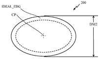
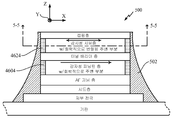
[0020] 도 1은, 구성 층들의 확장면(extending plane)에 대해 법선인 투영면(projection plane) 상에서, 하나의 예시적인 통상적 멀티-층 MTJ 디바이스에 대한 하나의 통상적인 멀티-층 필러 구조의 횡단면도이다.
[0021] 도 2는, "이상적인" 화학적/강자성 구조를 갖는 주변 영역을 나타내는 중첩된(superposed) 도면을 이용한, 도 1의 종래의 멀티-층 MTJ 디바이스의 하나의 강자성 층에 대한 도 1의 2-2로부터의 투영도이다.
[0022] 도 3a는, 종래의 에칭 시에 형성되는 MTJ 강자성 층들의 손상된 주변 영역들의 예시적인 공간적 양태(spatial aspect)들을 도시하는 중첩된 도면을 이용한 하나의 종래의 멀티-층 MTJ 디바이스의 하나의 종래의 멀티-층 필러 구조에 대한 도 1의 횡단면도이다.
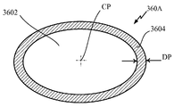
[0023] 도 3b는, 도 3a의 투영면 3-3 상에서의 중첩된 도면에 의해, 통상적 에칭에 대한, 도 3a의 종래의 멀티-층 MTJ 디바이스의 예시적 MTJ 강자성 층들 중 하나의 손상된 주변 영역들의 예시적인 공간적 양태들을 도시한다.
[0024] 도 4a는, 하나의 예시적인 실시예에 따라 구조화되고 그리고 이에 따라 형성된 하나의 예시적 화학적으로 변형된 엣지 멀티층 MTJ 디바이스의 양태들을 나타내는, 구성 층들의 확장면에 대해 법선인 투영면 상에서의 횡단면도이다.
[0025] 도 4b는, 하나의 예시적인 실시예에 따라 구조화되고 그리고 이에 따라 형성된 도 4a의 화학적으로 변형된 엣지 멀티-층 MTJ 디바이스의 하나의 화학적으로 변형된 엣지 강자성 층을 나타내는, 도 4a 4-4로부터의 투영도이다.
[0026] 도 5a는, 다른 예시적인 실시예에 따라 구조화되고 그리고 이에 따라 형성된 하나의 예시적 화학적으로 변형된 엣지 멀티층 MTJ 디바이스의 양태들을 나타내는, 구성 층들의 확장면에 대해 법선인 투영면 상에서의 횡단면도이다.
[0027] 도 5b는, 다른 예시적인 실시예에 따라 구조화되고 그리고 이에 따라 형성된 도 5a의 화학적으로 변형된 엣지 멀티-층 MTJ 디바이스의 하나의 화학적으로 변형된 엣지 강자성 층을 도시하는, 도 5a의 5-5로부터의 투영도이다.
[0028] 도 6a-도 6f는, 하나 또는 그 초과의 예시적인 실시예들에 따라 하나의 화학적으로 변형된 엣지 멀티-층 MTJ 디바이스를 제공하는 예시적 프로세스들 및 예시적 구조들을 설명하는, 구성 시작 및 인-프로세스 층들의 확장면에 대해 법선인 투영면 상에서의 횡단면도들의 스냅샷 시퀀스를 도시한다.
[0029] 도 7a-도 7f는, 다른 하나 또는 그 초과의 예시적인 실시예들에 따라 하나의 화학적으로 변형된 엣지 멀티-층 MTJ 디바이스를 제공하는 예시적 프로세스들 및 예시적 구조들을 설명하는, 구성 시작 및 인-프로세스 층들의 확장면에 대해법선인 투영면 상에서의 횡단면도들의 스냅샷 시퀀스를 도시한다.
[0030] 도 8은, 하나 또는 그 초과의 예시적인 실시예들에 따라 화학적으로 변형된 엣지 멀티-층 MTJ 디바이스들을 제공하는 다양한 양상들에 더해 동작들의 하나의 플로우차트 도면을 도시한다.
[0031] 도 9는, 다양한 예시적인 실시예들의 양상들에 따라, 화학적으로 변형된 엣지 멀티-층 MTJ 디바이스들을 갖고, 지지하고, 통합하고, 그리고/또는 채용하는 하나의 무선 통신 시스템, 및 화학적으로 변형된 엣지 멀티-층 MTJ 디바이스들을 제조하는 프로세스들의 일 시스템 도면을 도시한다.BRIEF DESCRIPTION OF THE DRAWINGS [0019] The accompanying drawings, which are found in the annexed drawings, are set forth to illustrate embodiments of the invention and are provided by way of illustration only, and not limitation of the embodiments.
[0020] FIG. 1 is a cross-sectional view of one typical multi-layer filler structure for one exemplary conventional multi-layer MTJ device, on a projection plane normal to the extending plane of the constituent layers to be.
[0021] FIG. 2 is a schematic cross-sectional view of the conventional ferromagnetic layer of FIG. 1 for a ferromagnetic layer of the conventional multi-layer MTJ device of FIG. 1 using a superposed view showing a peripheral region having an "ideal" chemical / -2 < / RTI >
[0022] FIG. 3a is a schematic diagram of one conventional multi-layer MTJ device using overlapping views showing exemplary spatial aspects of damaged peripheral regions of MTJ ferromagnetic layers formed during
[0023] FIG. 3B is a schematic view of a portion of one of the exemplary MTJ ferromagnetic layers of the conventional multi-layer MTJ device of FIG. 3A for the conventional etch, as shown in the overlapped view on the projection plane 3-3 of FIG. Illustrate exemplary spatial aspects.
[0024] FIG. 4A is a schematic diagram of an exemplary multi-layer MTJ device that is structured and thus formed according to one exemplary embodiment, showing aspects of an exemplary chemically modified edge multi-layer MTJ device, Fig.
[0025] FIG. 4B illustrates a chemically modified edge ferromagnetic layer of the chemically modified edge multi-layer MTJ device of FIG. 4A structured and thus formed according to one exemplary embodiment; FIGS. 4A 4 -4. ≪ / RTI >
[0026] FIG. 5a is a graphical representation of an exemplary multi-layer MTJ device structure that is structured and thus formed according to another exemplary embodiment, showing aspects of one exemplary chemically modified edge multi-layer MTJ device, Sectional view.
[0027] FIG. 5b is a cross-sectional view of a chemically-modified edge multi-layer MTJ device of FIG. 5a structured and thus formed according to another exemplary embodiment, 5-5.
[0028] Figures 6A-6F illustrate exemplary processes and exemplary structures for providing a chemically-modified edge multi-layer MTJ device in accordance with one or more exemplary embodiments. Lt; / RTI > shows a snapshot sequence of cross-sectional views on a projection plane that is normal to the extended surfaces of the start and in-process layers.
7A-7F illustrate exemplary processes and exemplary structures for providing a chemically modified edge multi-layer MTJ device in accordance with another or more exemplary embodiments. And a snapshot sequence of cross-sectional views on a projection plane that is normal to the expanded surface of the in-process layers.
[0030] FIG. 8 illustrates a flowchart of one of the operations in addition to the various aspects of providing chemically modified edge multi-layer MTJ devices in accordance with one or more exemplary embodiments.
[0031] FIG. 9 illustrates one wireless communication system that has, supports, integrates, and / or employs chemically modified edge multi-layer MTJ devices, according to aspects of various exemplary embodiments, Lt; RTI ID = 0.0 > MTJ < / RTI > devices.
[0032] 본 발명의 양상들은, 본 발명의 특정 실시예들에 관련된 후술하는 상세한 설명 및 관련 도면들에 개시된다. 대안적인 실시예들이 본 발명의 범위를 벗어나지 않고 고안될 수 있다. 추가적으로, 본 발명의 잘 알려진 엘리먼트들은 본 발명의 관련 세부사항들을 모호하게 하지 않기 위해 상세하게 설명되지 않거나 또는 생략될 것이다.[0032] Aspects of the present invention are set forth in the following detailed description and the associated drawings, in connection with specific embodiments of the invention. Alternate embodiments may be devised without departing from the scope of the present invention. In addition, well-known elements of the present invention will not be described in detail or will be omitted so as not to obscure the relevant details of the present invention.
[0033] 단어 "예시적인"은 "예, 예시, 또는 예증으로서 기능하는"을 의미하도록 본원에 이용된다. "예시적인"으로서 설명된 어떠한 실시예도 반드시 다른 실시예들에 비해 선호되거나 또는 유리한 것으로서 해석되는 것은 아니다. 유사하게, 용어 "본 발명의 실시예들"은, 본 발명의 모든 실시예들이 논의된 특징, 이점, 또는 동작 모드를 포함하는 것을 요구하지 않는다. [0033] The word "exemplary" is used herein to mean "serving as an example, example, or illustration." Any embodiment described as "exemplary " is not necessarily to be construed as preferred or advantageous over other embodiments. Similarly, the term "embodiments of the present invention" does not require that all embodiments of the present invention include the discussed features, advantages, or modes of operation.
[0034] 본원에 이용된 용어는, 특정한 실시예들에 따라 예시들을 설명하는 목적을 위한 것이며, 본 발명의 실시예들을 제한하도록 의도되지 않는다. 본원에 이용된 바와 같이, 단수 형태들은, 문맥상 명확하게 달리 명시하지 않는 한, 복수 형태들도 또한 포함하는 것으로 의도된다. 용어들 "포함하다(comprises)", "포함하는(comprising)", "구비하다(includes)" 및/또는 "구비하는(including)"은, 본 명세서에 이용되는 경우, 언급된 특징들, 정수들, 단계들, 동작들, 엘리먼트들, 및/또는 컴포넌트들의 존재를 특정하지만, 하나 또는 그 초과의 다른 특징들, 정수들, 단계들, 동작들, 엘리먼트들, 컴포넌트들, 및/또는 이들의 그룹들의 존재 또는 부가를 불가능하게 하는 것은 아니라는 것을 더 이해할 것이다. [0034] The terminology used herein is for the purpose of describing the examples in accordance with the specific embodiments, and is not intended to limit the embodiments of the invention. As used herein, singular forms are intended to also include the plural forms, unless the context clearly dictates otherwise. The terms " comprises, "" comprising," " comprises, " and / or "including ", when used in this specification, Elements, steps, operations, elements, and / or components, but also may involve one or more other features, integers, steps, operations, elements, components, and / It will be understood that they do not preclude the presence or addition of groups.
[0035] 게다가, 수많은 실시예들이, 예를 들어, 컴퓨팅 디바이스의 엘리먼트들에 의해 수행될 동작들의 시퀀스들과 관련하여 설명된다. 본원에 설명된 다양한 동작들은, 특정 회로들(예컨대, 주문형 집적회로들(ASIC들))에 의해, 하나 또는 그 초과의 프로세서들에 의해 실행되는 프로그램 명령들에 의해, 또는 이 둘의 조합에 의해 수행될 수 있다는 것을 인식할 것이다. 추가적으로, 본원에 설명된 동작들의 이러한 시퀀스는, 실행시에, 관련 프로세서로 하여금 본원에 설명된 기능을 수행하게 하는 대응 세트의 컴퓨터 명령들이 저장된 임의의 형태의 컴퓨터 판독가능 저장 매체 내에서 전체적으로 구현되는 것으로 고려될 수 있다. 따라서, 본 발명의 다양한 양상들은 다수의 상이한 형태들로 구현될 수 있고, 이 형태들 모두는 청구된 청구대상의 범위 내에 있는 것으로 고려된다. 이에 더해, 본원에 설명된 실시예들 각각에 대해, 예시적인 구현들 및 형태들은, 예를 들어, 설명된 동작을 수행하도록 "구성된 로직"으로서 설명될 수 있다.[0035] In addition, numerous embodiments are described in connection with, for example, sequences of operations to be performed by elements of a computing device. The various operations described herein may be performed by specific circuits (e.g., application specific integrated circuits (ASICs)), by program instructions executed by one or more processors, or by a combination of the two As will be appreciated by those skilled in the art. Additionally, such a sequence of operations described herein may be implemented entirely within any form of computer-readable storage medium having stored thereon a corresponding set of computer instructions for causing the associated processor to perform the functions described herein . ≪ / RTI > Accordingly, various aspects of the present invention may be embodied in many different forms, all of which are considered to be within the scope of the claimed subject matter. In addition, for each of the embodiments described herein, exemplary implementations and aspects may be described as "configured logic" to perform, for example, the described operations.
[0036] 당업자들은 정보 및 신호들이 다양한 상이한 기술들 및 기법들 중 임의의 것을 이용하여 표현될 수 있다는 것을 이해할 것이다. 예를 들어, 전술한 설명 전반에 걸쳐 참조될 수 있는 데이터, 명령들, 커맨드들, 정보, 신호들, 비트들, 심볼들 및 칩들은 전압들, 전류들, 전자기파들, 자기장들 또는 자기 입자들, 광 필드들, 전자 스핀 입자들, 전자 스핀들, 또는 이들의 임의의 결합에 의해 표현될 수 있다. [0036] Those skilled in the art will understand that information and signals may be represented using any of a variety of different technologies and techniques. For example, data, instructions, commands, information, signals, bits, symbols, and chips that may be referenced throughout the above description may refer to voltages, currents, electromagnetic waves, , Light fields, electron spin particles, electron spindles, or any combination thereof.
[0037] 게다가, 본원에 개시된 실시예들과 관련하여 설명되는 다양한 예시적인 논리 블록들, 모듈들, 회로들 및 알고리즘 단계들은 전자 하드웨어, 컴퓨터 소프트웨어, 또는 이들 둘의 조합들로서 구현될 수 있다는 것이 당업자들에게 인식될 것이다. 하드웨어와 소프트웨어의 상호교환 가능성을 명료하게 설명하기 위해, 다양한 예시적인 컴포넌트들, 블록들, 모듈들, 회로들 및 단계들이 그들의 기능과 관련하여 앞서 일반적으로 도시되어 있다. 본 개시물을 판독하는 것으로부터 당업자들에 의해 용이하게 인식되는 바와 같이, 이러한 기능이 하드웨어로 구현되는지 또는 소프트웨어로 구현되는지, 또는 하드웨어와 소프트웨어의 조합으로 구현되는지는 특정 애플리케이션 및 전체 시스템에 부과되는 설계 제약들에 의존한다. 당업자들은 설명된 기능을 각각의 특정한 애플리케이션에 대하여 다양한 방식들로 구현할 수 있으나, 이러한 구현 결정들은 본 발명의 범위를 벗어나게 하는 것으로 해석되어서는 안된다. [0037] Moreover, it is to be understood that the various illustrative logical blocks, modules, circuits, and algorithm steps described in connection with the embodiments disclosed herein may be implemented as electronic hardware, computer software, Will be recognized. To clearly illustrate the interchangeability of hardware and software, various illustrative components, blocks, modules, circuits, and steps have been generally shown above in the context of their functionality. Whether such functionality is implemented in hardware, or in software, or in a combination of hardware and software, as will be readily appreciated by those skilled in the art from reading this disclosure, It depends on design constraints. Skilled artisans may implement the described functionality in varying ways for each particular application, but such implementation decisions should not be interpreted as causing a departure from the scope of the present invention.
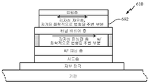
[0038] 도 1은 MTJ 디바이스들의 종래의 제조 시에 형성된 멀티-층 자기 터널 정션 디바이스(100)(이하, "멀티-층 MTJ 디바이스"(100))의 횡단면도를 도시한다. 도 1의 멀티-층 MTJ 디바이스(100)는, 예를 들어, 판독/기록 액세스 및 다른 회로를 생략하는 간략화된 형태로 도시되며, 여기서 이들에 대한 설명은 본 개시물의 관점을 갖는 당업자들이 예시적인 실시예들의 하나 또는 그 초과에 따른 신규의 개념들 및 프랙티스(practice)를 이해하게 하는데 필수적이지는 않다. 용어 "멀티-층 MTJ 디바이스"(100)에서 이용되는 것과 같은 "디바이스"가 완전하게 제조된 디바이스로 제한되지 않는다는 점이 이해될 것이다. 예를 들어, 멀티-층 MTJ 디바이스(100)는 "인-프로세스" 구조일 수 있는데, 즉, 그 도시된 구조의 부분들(별도로 라벨링되지 않음)은 종래의 MTJ 제조 기법들에 따라 후속 프로세싱에 의해 제거될 수 있거나 또는 변형될 수 있다.[0038] FIG. 1 shows a cross-sectional view of a multi-layer magnetic tunnel junction device 100 (hereinafter "multi-layer MTJ device" 100) formed in the conventional manufacture of MTJ devices. The
[0039] 도 1을 참조하면, 멀티-층 MTJ 디바이스(100)는 "MTJ 필러"(102)로서 본 개시물에 명명된 멀티-층 구조를 포함할 수 있다. MTJ 필러(102)는 종래의 MTJ 기판(104)(이하, "기판(104)"로 참조됨) 상에 배열될 수 있다. MTJ 필러(102)는, 스택된 층들, 예를 들어, 저부 전극(106), 시드층(108), 반-강자성(AF) 피닝 층(110), 강자성 피닝된 층(112), 터널 배리어 층(114), 강자성 자유층(116) 및 캡핑 층(118)을 포함한다. 설명된 층들 각각은, X-Y 평면에서 확장하는 것으로서, 도 1의 X-Z 투영면에 대하여 배향되며, 여기서 X는 수평축이고, Y는 X-Z 투영면에 대하여 법선이며, 이들 각각은 Z 방향에서 (별도로 라벨링되지 않은 것으로 도시됨) 개별적인 두께를 갖는다.[0039] Referring to FIG. 1, a
[0040] 도 1을 여전히 참조하여, 저부 전극(106), 시드층(108), AF 피닝 층(110), 강자성 피닝된 층(112), 터널 배리어 층(114), 강자성 자유층(116) 및 캡핑 층(118) 각각의 재료들, 치수들(예를 들어, 두께), 기능들, 및 동작 메커니즘들은 종래의 기법들에 따를 수 있다. 따라서, 예시적인 실시예들에 따른 예시적인 양상들 및 동작들의 이후의 설명에 대해 부수적인 것을 제외하고는, 추가적으로 상세화된 설명은 생략된다.1, the
[0041] 당업자들에 의해 이해되는 바와 같이, 저부 전극(106), 시드층(108), AF 피닝 층(110), 강자성 피닝된 층(112), 터널 배리어 층(114), 강자성 자유층(116) 및 캡핑 층(118)의 도 1의 배열인 도 1의 MTJ 필러(102)는 다양한 종래의 MTJ 디바이스들(도면들에는 도시되지 않음)에서 발견된 구조적 양상들을 예시화할 수 있다. 도 1에 도시된 바와 같은 구조적 특징들을 갖는 종래의 MTJ 디바이스들이 추가적인 층들, 예를 들어, 도시된 층들 사이에 추가적인 금속 산화물 층들을 포함할 수 있다는 점은 당업자들에 의해 또한 이해될 것이다. 종래의 MTJ 디바이스들은 또한, 멀티-층 구조들로서 특정한 도시된 층들, 예를 들어, 강자성 자유층(116)을 형성할 수 있다.As will be understood by those skilled in the art, the
[0042] 도 1을 여전히 참조하면, MTJ 필러(102)와 동일한 또는 이에 필적할만한 멀티-층 MTJ 디바이스들에 대한 종래의 제조 기법들은, 예시적 기판(104)과 같은 기판상에, 층들의 도 1의 단면을 갖는 (X-Y 평면에서의 확장과 관련하여) 더 큰 멀티-층 MTJ 구조(명료하게 도시되지 않음)를 형성함으로써 시작할 수 있다는 점이 당업자들에게 또한 이해될 것이다. 더 큰 멀티-층 구조는, "MTJ 멀티-층 시작 구조"로 지칭될 수 있다. MTJ 멀티-층 시작 구조는, 예를 들어, X 및 Y 방향들에서, 도 1의 예시적 MTJ 필러(102)의 DM1 및 DM2 각각보다 실질적으로 더 큰 거리를 확장할 수 있다. 종래의 MTJ 제조 기법들은 그후, 나머지 구조로서 MTJ 필러(102)를 획득하기 위해, 예를 들어, 하나 또는 그 초과의 에칭 프로세스들에 의해 MTJ 멀티-층 시작 구조로부터 재료를 제거할 수 있다. 공지된 종래의 제조 장비 및 시스템들이 채용될 수 있으며, 이에 따라 예시적인 실시예들에 따른 예시적 양상들 및 동작들의 이후의 설명에 부수적인 것을 제외하고는, 추가적인 세부화된 설명은 생략된다.[0042] Still referring to FIG. 1, conventional fabrication techniques for multi-layer MTJ devices, which are the same as or comparable to
[0043] 예시적인 실시예들에 따라 변형될 수 있고, 그리고/또는 환경을 예시하고, 환경에 관련하며, 환경일 수 있는 공지된 종래의 MTJ 제조 기법들의 특정 특징들을 설명하기 전에, MTJ 필러(102)의 강자성 자유층(116)과 같은 층들의 특정한 이상적인 구조 양상들이 논의될 것이다.[0043] Before describing certain features of known conventional MTJ fabrication techniques that may be modified in accordance with the exemplary embodiments and / or illustrate the environment, be environment related, and be environment, MTJ fillers 0.0 > 116 < / RTI > of the ferromagnetic
[0044] 도 2는, 강자성 자유층(116)의 하나의 가설적 이상적 구조(200)에 대한, 도 1의 투영 2-2으로부터의 평면도이다. 강자성 자유층(116)의 설명된 가설적 이상적 구조(200)는 또한 강자성 피닝된 층(112)의 가설적 이상적 구조(명료하게 도시되지 않음)를 특징화할 수 있는 것으로 이해될 것이다. 가설적 이상적 구조(200)는, "이상적인" 화학적/강자성 구조를 갖는 IDEAL_EDG로서 중첩된 도면에 의해 인위적으로 경계가 표시된 주변 영역을 갖는다. 이 설명의 목적들을 위해, "이상적인" 화학적/강자성 구조는 화학적 조성을 의미하며, IDEAL_EDG 영역의 자체 강자성 특성들은 가설적 이상적 구조(200)의 나머지 영역들, 즉, IDEAL_EDG에 의해 둘러싸이고 경계가 정해진 영역과 동일하다. 도 2를 참조하는데 있어 편의를 위해, IDEAL_EDG 내부에서 강자성 층의 가설적 이상적 구조(200)의 영역은 "메인 영역"으로 명명될 것이다.[0044] Figure 2 is a plan view from projection 2-2 of Figure 1 for one hypothetical
[0045] 도 2를 여전히 참조하면, IDEAL_EDG는 에너지의 인가 없이 그리고 어떠한 화학적 반응에 영향을 주지 않고 나머지 구조로서 MTJ 필러(102)를 획득하기 위해 멀티-층 MTJ 시작 구조로부터 재료의 가설적 제거를 초래하는 것으로 가정된다. IDEAL_EDG는 따라서 임의의 구조적 변화들의 묘사는 아니다. 반대로, 앞서 설명된 바와 같이, 가설적 이상적 구조(200)는 균일한 화학적 형성(make-up) 및 강자성 특징들을 갖는 것으로 가정된다. IDEAL_EDG는 오직 참조 위치이며, 여기서 "위치"는, 이후의 섹션들에서 더욱 상세하게 설명되는 것과 같이 MTJ 필러(102)와 같은 구조들에서 실제 제조된 예시적인 강자성 층들 내에서 유사하게 위치된 영역들에서의 구조와 비교하기 위해, 맨끝의(extreme) 엣지 EDG로부터 내측으로의(중심 CP를 향하는) 방사상 거리에 의해 정의된다.[0045] Still referring to FIG. 2, IDEAL_EDG provides a hypothetical removal of material from the multi-layer MTJ start structure to obtain the
[0046] 본 개시물에 이전에 설명된 바와 같이, 도 2의 IDEAL_EDG는 에너지의 인가 없이 그리고 임의의 화학적 반응에 영향을 주지 않고 나머지 구조로서 MTJ 필러(102)를 획득하기 위해 멀티-층 MTJ 시작 구조로부터 재료의 가설적 제거를 가정한다. 그러나, 나머지 구조로서 MTJ 필러(102)를 획득하기 위해 멀티-층 MTJ 시작 구조로부터 재료를 제거하기 위한 공지된 에칭 기법들은 에너지를 가하고, 이에 따라 바람직하지 않은 화학적 반응들, 즉, 화학적 손상을 초래할 수 있다. 화학적 반응들은, 예를 들어, 강자성 자유층(116)의 주변부에서 MTJ 필러(102)를 형성하는 층들의 주변부(또는 주변 엣지 영역)에서의 산화, 질화, 또는 불화 중 하나 또는 그 초과를 포함할 수 있다. 이에 더해, 다음 프로세스 단계로 진행하는 천이 프로세스들, 및 에칭 프로세스에 후속하는 CVD(화학적 기상 증착)은 강자성 층들의 주변부에 화학적 손상을 생성할 수 있다.As previously described in this disclosure, the IDEAL_EDG of FIG. 2 can be used to initiate a multi-layer MTJ start to acquire the
[0047] 도 3a는, 도 1 상에 중첩된 도면으로, 멀티-층 MTJ 필러(102)와 실질적으로 동일하게 배열되지만 도 1의 강자성 자유층(116) 대신에 화학적으로 손상된 주변 엣지 강자성("손상된 PEFM") 자유층(360)을 갖는 MTJ 필러 구조(300)의 단면을 도시하는 정면 투영 절취도를 도시한다. 용어 "손상된 PEFM"은 단순히 "화학적으로 손상된 주변 엣지 강자성"의 축약어이며 어떠한 추가적인 의미도 갖지 않는다는 점이 이해될 것이다. MTJ 필러 구조(300)는 또한, 도 1의 강자성 피닝된 층(112) 대신에 손상된 PERM 피닝된 층(380)을 나타낸다. 그렇지만, 예시적인 실시예들이 손상된 PEFM 자유층(360) 및 손상된 REFM 피닝된 층(380) 중 임의의 하나 또는 둘 다를 이용하여 실행될 수 있다는 점이 이해될 것이다.[0047] FIG. 3A is a diagram superimposed on FIG. 1, which is arranged substantially the same as the
[0048] 도 3b는, 예시적 "메인" 또는 "중심" 영역(3602)을 나타내는 중첩된 도면을 통해, 도 3a 3-3으로부터 투영도로 보여진 예시적 화학적으로 손상된 주변 영역(3604)에 의해 둘러싸인 손상된 PEFM 자유층(360)의 슬라이스(360A)를 도시한다.[0048] Figure 3b illustrates a top view of an exemplary "main" or "center"
[0049] 화학적으로 손상된 주변 영역(3604)은 종래의 에칭 기법들 및 관련 프로세싱, 예를 들어, 화학 기상 증착(CVD)으로부터 발생할 수 있는 화학적 손상의 하나의 일반적인 분포를 나타낸다. 이와 유사하게, (오직 도 3a에만 도시된) 손상된 PERM 피닝된 층(380)은 손상되지 않은 "메인" 또는 "중심" 영역(3802) 및 화학적으로 손상된 주변 영역(3804)을 포함하여, 종래의 에칭 기법들 및 관련 프로세싱으로부터 발생할 수 있는 앞서-설명된 화학적 손상의 하나의 일반적인 분포를 나타낸다.[0049] The chemically damaged
[0050] 명료함을 위해, 다양한 예시들은 오직 손상된 PEFM 자유층(360)과 관련하여 설명된다. 그렇지만, 그렇지 않은 것으로 명료하게 언급되거나 또는 내용으로부터 명료하게 행해진 것을 제외하면, 예시들 및 다양한 양상들은 손상된 PEFM 피닝된 층(380)과 관련하여, 또는 손상된 PEFM 자유층(360) 및 손상된 PEFM 피닝된 층(380) 둘 다와 관련하여 실행될 수 있다는 점이 이해될 것이다.[0050] For clarity, various examples are described with respect to only the damaged PEFM
[0051] 도 3a 및 도 3b를 참조하면, 손상된 PEFM 자유층(360)의 화학적으로 손상된 주변 영역(3604)은, 손상된 PEFM 자유층(360)이 에칭되었던 MTJ 멀티-층 시작 구조의 층을 형성하는 재료(명료하게 도시되지 않음)의 산화, 질화, 또는 둘 다를 나타낼 수 있다. 산화, 질화, 또는 둘 다는, 예를 들어, 에칭 프로세스들 동안 도입된, 예를 들어, 질소 또는 산소 또는 둘 다로부터 발생할 수 있다. 화학적으로 손상된 주변 영역(3604)를 형성했던 산화, 질화, 또는 둘 다의 특정 화학적 형성은, 손상된 PEFM 자유층(360)이 형성되었던 MTJ 멀티-층 시작 구조의 화학적 형성에 적어도 부분적으로 의존한다.3A and 3B, the chemically damaged
[0052] 예를 들어, 일 양상에서, 손상된 PEFM 자유층(360)은 연강자성(soft ferromagnetic) 재료, 예를 들어, 철(Fe)의 층으로부터 에칭될 수 있다. 강자성 Fe의 질화는 경자성(hard magnetic) 재료들, 예를 들어, FeN을 생성할 수 있다. 화학적으로 손상된 주변 영역(3604)의 경자성 FeN 조성은, 제조가 완료되었을 때 그리고 이것이 동작 MTJ 디바이스의 일부일 때, 손상된 PEFM 자유층(360)의 성능 특징들에서 뜻밖의 효과들을 가질 수 있다. 뜻밖의 효과들의 예시는, 예를 들어, 큰 자기 포화(Ms), 큰 오프셋 자기 필드(Hoff), 더 낮은 교환 상수, 감소된 터널 자기저항(TMR), 및/또는 R-H 루프의 열화의 단독 또는 조합일 수 있다.[0052] For example, in one aspect, the damaged PEFM
[0053] 도 3a-도 3b를 계속해서 참조하여, 화학적으로 손상된 주변 영역(3604)은 바깥쪽 엣지(도시되지만 별도로 라벨링되지 않음)에 또는 그와 실질적으로 일치하는 바깥쪽 극값을 가질 수 있고, 기하학적 중심 CP에 대해 방사상 방향에서 측정된 평균 깊이 DP까지 연장할 수 있다. 예시적 목적들을 위해, 손상된 PEFM 자유층(360)은 도 1 및 도 2에서 라벨링된 "DM1" 및 "DM2"와 동일할 수 있는 (도시되지만 도 3b 상에서 라벨링되지 않은) 외경(major diameter) 및 내경(minor diameter)을 갖는 타원형 형상을 갖는 것으로 가정될 것이다. 직경(예를 들어, DM1, DM2, 또는 DM1, DM2의 평균)에 대한 평균 깊이 DP의 비율의 도 3b의 그래픽 표현은 도면들에서 가시성을 위한 것이며, 직경에 대한 DP의 비율의 수치적 값을 나타내는 것을 의도하지 않는다는 점이 이해될 것이다.[0053] Continuing with FIG. 3A-FIG. 3B, the chemically damaged
[0054] MTJ 디바이스들의 종래의 제조에서, 도 1의 MTJ 필러(102)와 같은 필러들을 형성하기 위한 에칭 이후에, 하나 또는 그 초과의 층들이 적용될 수 있다는 점이 주목할 만하다. 에칭이 손상 영역들을 형성하는 종래의 제조에서의 예시들에서, 도 3a-도 3b의 화학적으로 손상된 주변 영역(3604)에 의해 도시된 바와 같이, 하나 또는 그 초과의 층들이 이러한 손상된 주변 영역들 상에 적용될 수 있다는 점이 추가로 주목할 만하다. 이러한 층들은, 종래의 MTJ 제조 기술에서 "보호층들"로 지칭될 수 있다.[0054] It should be noted that, in the conventional manufacture of MTJ devices, one or more layers may be applied after etching to form fillers such as the
[0055] 이후의 섹션들에서 더욱 상세하게 설명되는 바와 같이, 일 실시예에 따라, 전체 또는 적어도 충분한 비율로 선택된 화학적으로 손상된 주변 영역(3604)은 완전하게 강자성 데드(ferromagnetic dead)인 "화학적으로 변형된 주변 부분"(도 3a 및 도 3b에는 도시되지 않음)으로 트랜스포밍될 수 있다. 관련 신규 구조(들)와 함께, 화학적으로 변형된 주변 부분은, 이후 섹션들에서 더욱 상세하게 설명된 다른 이점들 중에서, 종래의 MTJ 자기 층 기법들에서 발생할 수 있는 화학적 엣지 손상을 일으키는 자기적 특성들에 있어서의 앞서-설명된 열화의 상당한 감소 및/또는 제거를 제공할 수 있다.[0055] As will be described in more detail in the following sections, according to one embodiment, the chemically damaged
[0056] 일 양상에서, 자기적으로 데드인 화학적으로 변형된 주변 부분으로의 화학적으로 손상된 주변 영역(3604)의 트랜스포메이션(transformation)은 산화 프로세스를 포함할 수 있다. 관련 양상에서, 자기적으로 데드인 화학적으로 변형된 주변 부분으로의 화학적으로 손상된 주변 영역(3604)의 트랜스포메이션은 질화 프로세스를 포함할 수 있다. 추가적인 양상에서, 자기적으로 데드인 화학적으로 변형된 주변 부분으로의 화학적으로 손상된 주변 영역(3604)의 트랜스포메이션은 불화 프로세스를 포함할 수 있다. 다른 양상에서, 자기적으로 데드인 화학적으로 변형된 주변 부분으로의 화학적으로 손상된 주변 영역(3604)의 트랜스포메이션은, 질화 프로세스, 산화 프로세스, 및/또는 불화 프로세스 중에서 임의의 2개 또는 그 초과의 조합을 포함할 수 있다.[0056] In an aspect, the transformation of the chemically damaged
[0057] 다양한 예시적인 실시예들은, 이후 섹션들에서 더욱 상세하게 설명된 바와 같이, 나머지, 즉, 중심 영역의 손상되지 않은 결정 구조상에서보다 인-프로세스 강자성 층의 화학적으로 손상된 주변 영역의 손상된 결정 구조상에서 상당히 더 빠르게 작용하는 이러한 프로세스들을 활용 및 이용하도록 구성된 양상들에서, 질화 프로세스, 산화 프로세스 및 불화 프로세스 중 하나 또는 그 초과를 적용한다.[0057] The various exemplary embodiments can be used to determine the remaining, ie, damaged, crystals of the chemically damaged peripheral region of the in-process ferromagnetic layer than on the undamaged crystal structure of the central region, as described in more detail in subsequent sections In aspects configured to utilize and utilize these processes that operate significantly faster in structure, one or more of the nitriding process, the oxidizing process, and the fluorinating process is applied.
[0058] 이 양상에 더해, 화학적으로 변형된 주변 영역을 형성하기 위해 인-프로세스 또는 중간 단계 강자성 층의 화학적으로 손상된 주변 영역의 허용가능한 비율이 산화, 질화, 또는 불화될 때까지, 질화 프로세스, 산화 프로세스, 불화 프로세스, 또는 이들의 임의의 조합이 계속될 수 있다. 인-프로세스 또는 중간 단계 강자성 층의 손상되지 않은 중앙 영역의 허용불가한 산화 또는 질화가 야기되기 전에 질화 프로세스, 산화 프로세스 또는 불화 프로세스 또는 이 프로세스들의 임의의 조합이 종결할 수 있다는 점이 당업자에 의해 이해될 것이다. 즉, 일 양상에서, 질화 프로세스, 산화 프로세스 또는 불화 프로세스, 또는 이 프로세스들의 임의의 조합은, 화학적으로 손상된 주변 영역 내부로의 깊이를 증가시키는 것을 계속할 수 있고, 바람직하게는, 그 손상된 영역의 깊이에 도달할 때 또는 도달하기 바로 전에 종결할 수 있다. 인식되는 바와 같이, 이러한 프로세싱은 자신의 중심으로부터 방사상 라인을 따라 일정하게 양호한 강자성 특성을 갖는 강자성 층을 생성할 수 있으며, 그후 강자성 데드 특성으로의 급격한 구배 천이(sharp gradient transition)가 후속된다.[0058] In addition to this aspect, it is also possible to use a nitridation process, a nitridation process, or a combination thereof, until an acceptable percentage of the chemically damaged peripheral regions of the in-process or intermediate ferromagnetic layer is oxidized, An oxidation process, a fluorination process, or any combination thereof. It is understood by those skilled in the art that nitridation, oxidation, or fluorination processes or any combination of these processes may be terminated before unacceptable oxidation or nitridation of the intact central region of the in-process or intermediate ferromagnetic layer is caused Will be. That is, in one aspect, the nitriding process, the oxidizing process, or the fluorinating process, or any combination of these processes, can continue to increase the depth into the chemically damaged surrounding area, and preferably the depth of the damaged area Or may be terminated shortly before reaching. As will be appreciated, this processing can produce a ferromagnetic layer with uniformly good ferromagnetic properties along its radial line from its center, followed by a sharp gradient transition to ferromagnetic dead characteristics.
[0059] 일 양상에서, 중간 단계 또는 인-프로세스 강자성 층은, 강자성 엘리먼트, 예를 들어, 코발트(Co), 철(Fe), 니켈(Ni) 및/또는 붕소(Bo), 또는 강자성 엘리먼트들의 화합물들, 예를 들어, CoFeB, CoFe, NiFe, 또는 이들의 임의의 조합 또는 서브-조합을 포함할 수 있다. 이 양상에 따르면, 산화 프로세스에 대해 추가로, 화학적으로 변형된 주변 영역은, FeOx, CoOx, CoFeOx, NiFeOx, 및/또는 BOx 중에서 하나 또는 그 초과를 포함할 수 있다. 유사하게, 질화 프로세스에 대해 추가적인 양상에서, 주변 화학적으로 변형된 부분은 FeNx, CoNx, CoFeNx, NiFeNx 및/또는 BNx로부터 하나 또는 그 초과를 포함할 수 있다. 불화 프로세스에 대해 추가적인 양상에서, 화학적으로 변형된 주변 영역은 CoFx, FeFx, NiFeFx, BFx 및/또는 CoFeFx 중 하나 또는 그 초과를 포함할 수 있다. 산화, 질화 및 불화 중에서 2개의 조합들 또는 서브-조합들을 채용하는 양상들은, 앞서-식별된 화학적 화합물들의 조합들을 포함할 수 있다.[0059] In an aspect, the intermediate step or in-process ferromagnetic layer comprises a ferromagnetic element such as cobalt (Co), iron (Fe), nickel (Ni) and / or boron (Bo) Compounds, e. G., CoFeB, CoFe, NiFe, or any combination or sub-combination thereof. According to this aspect, in addition to the oxidation process, the chemically modified peripheral region may comprise one or more of FeOx, CoOx, CoFeOx, NiFeOx, and / or BOx. Similarly, in an additional aspect to the nitridation process, the ambient chemically modified portion may comprise one or more of FeNx, CoNx, CoFeNx, NiFeNx and / or BNx. In a further aspect of the fluorination process, the chemically modified peripheral region may comprise one or more of CoFx, FeFx, NiFeFx, BFx and / or CoFeFx. Aspects employing two combinations or sub-combinations among oxidation, nitridation, and fluorination may include combinations of the previously-identified chemical compounds.
[0060] 다른 양상에서, 화학적으로 변형된 주변 영역으로의 화학적으로 손상된 주변 영역(3604)의 트랜스포메이션 이후에, 다양한 예시적인 실시예들에 따라 산화, 질화, 및/또는 불화, 또는 이들의 임의의 조합에 의해, 화학적으로 변형된 주변 부분의 전부 또는 대부분을 제거하기 위해 트림(trim) 또는 이온 밀링 프로세스가 수행될 수 있다.[0060] In another aspect, after the transformation of the chemically damaged
[0061] 다른 양상에서, 화학적으로 변형된 주변 부분의 전부 또는 대부분을 제거하는 양상과 함께 또는 이러한 제거를 수행하지 않고, 보호층이 적용될 수 있다. 일 양상에서, 보호층은 산화물 층 또는 질화물 층, 예를 들어, AlOx일 수 있다.[0061] In another aspect, a protective layer can be applied with or without removing all or most of the chemically modified peripheral portion. In an aspect, the protective layer may be an oxide layer or a nitride layer, for example AlOx.
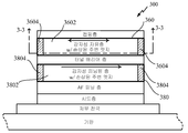
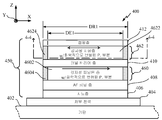
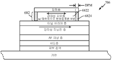
[0062] 도 4a는, 구성 층들의 확장 X-Y 평면에 법선인 투영면 X-Z 상에서의 단면도이며, 이는 하나 또는 그 초과의 예시적인 실시예들에 따라 구조화되고 이에 따라 형성된 하나의 예시적 화학적으로 변형된 엣지("CME") 멀티-층 MTJ 디바이스(400)의 양상들을 나타낸다. 용어 "CME"는 단순히 "화학적으로 변형된 엣지"에 대한 축약어이며, 어떠한 추가적인 의미도 갖지 않는다는 점이 이해될 것이다. 도 4b는, 하나의 예시적인 실시예에 따라 구조화되고 이에 따라 형성된 도 4a의 CME 멀티-층 MTJ 디바이스(400)의 일 CME 강자성 층을 나타내는 도 4a의 4-4로부터의 투영도이다.[0062] FIG. 4A is a cross-sectional view on a projection plane XZ, which is normal to the extended XY plane of the constituent layers, which is structured according to one or more exemplary embodiments and formed by one exemplary chemically modified edge ("CME")
[0063] 도 4a의 CME 멀티-층 MTJ 디바이스(400)는, 예를 들어, 판독/기록 액세스 및 다른 회로를 생략하는 간략화된 형태로 도시되며, 본 개시물을 검토할 때, 당업자들에게, 이들에 대한 설명이, 하나 또는 그 초과의 예시적인 실시예들에 따른 신규의 개념들 및 프랙티스를 이해하는데 필수적인 것은 아니다. 용어 "CME 멀티층 MTJ 디바이스"(400) 또는 "화학적으로 변형된 엣지 멀티-층 MTJ 디바이스"(400)에서 이용되는 것과 같은 "디바이스"는 임의의 예시적인 실시예들에 따라, 완전하게 제조된 디바이스들로 프랙티스들을 제한하는 것으로 의도되지 않는다는 점이 이해될 것이다. 예를 들어, CME 멀티-층 MTJ 디바이스(400)는 "인-프로세스" 구조일 수 있으며, 즉, 자체 도시된 구조의 부분들(별도로 라벨링되지 않음)은 종래의 MTJ 제조 기법들에 따라 후속 프로세싱에 의해 제거되거나 또는 변형될 수 있다.[0063] The CME
[0064] 편의를 위해, 도 4a-도 4b의 CME 멀티-층 MTJ 디바이스(400)는 도 1의 멀티-층 MTJ 디바이스(100)의 일반적인 스택 구성을 갖는다. 이러한 예시는, 예시적인 실시예들에 특정되지 않은 추가적인 구조들의 도입 및 설명을 요구하지 않고 신규의 양상들에 대해 촛점을 맞추는 것을 보조하도록 이용된다는 점이 이해될 것이다. 당업자들에 의해 용이하게 인식되는 바와 같이, 본 개시물을 판독할 때, 다양한 예시적인 실시예들에 따른 프랙티스들이 도 1의 멀티-층 MTJ 디바이스(100)의 일반적인 스택 구성을 적응하는 구조들에 제한되지는 않는다.[0064] For convenience, the CME
[0065] 도 4a를 참조하면, CME 멀티-층 MTJ 디바이스(400)는 MTJ 기판(402)(이하, "기판"(402)), 및 기판(402) 상에 배치된 저부 전극(404)을 포함할 수 있다. 기판(402) 및 저부 전극(404)은, 종래의 MTJ 기법들에 따라 구조화되고 형성될 수 있다. 저부 전극(404)의 (단면도로 도시되지만, 별도로 라벨링되지 않는) 상부 표면 상의 기판(402) 위에는 멀티-층 필러 구조(450)(이하, "MTJ" 필러(450))가 있을 수 있다. MTJ 필러(450)는, 저부-상단 순서(즉, "Z" 축의 화살표 방향)로, 시드층(406), AF 피닝 층(408), 화학적으로 변형된 엣지("CME") 강자성 피닝된 층(460), 터널 배리어 층(410), CME 강자성 자유층(462) 및 캡핑층(412)을 포함할 수 있다. 일 양상에서, CME 강자성 피닝 층(460)은 메인 영역(4602) 및 화학적으로 변형된 주변 영역(4604)을 포함할 수 있다. 추가적인 양상에서, CME 강자성 자유층(462)은 메인 영역(4622) 및 화학적으로 변형된 주변 부분(4624)을 포함할 수 있다. 일 양상에서, CME 강자성 피닝된 층(460)의 메인 영역(4602)은 CoFeB 또는 CoFe, 또는 둘 다와 같은 강자성 재료들을 포함할 수 있다. 하나의 관련 양상에서, CME 강자성 피닝된 층(460)의 화학적으로 변형된 주변 영역(4604)은 FeOx, CoOx, CoFeOx, BOx, FeNx, CoNx, CoFeNx, BNx, FeFx, CoFx, CoFeFx, 및/또는 BFx 그리고 이들 화학적 화합물들 중 임의의 조합 또는 서브-조합을 포함할 수 있다.4A, a CME
[0066] 도 4a를 계속 참조하면, 일 양상에서, CME 강자성 자유층(462)의 메인 영역(4622)은 CoFeB, CoFe 및 NiFe 중 임의의 하나, 또는 이들의 임의의 조합 또는 서브조합을 포함할 수 있다. 하나의 관련 양상에서, CME 강자성 자유층(462)의 화학적으로 변형된 주변 영역(4624)은, FeOx, CoOx, CoFeOx, BOx, FeNx, CoNx, CoFeNx, BNx, FeFx, CoFx, CoFeFx, 및/또는 BFx 또는 이러한 화학적 화합물 중 임의의 조합 또는 서브-조합을 포함할 수 있다.4a, in one aspect, the
[0067] CME 강자성 자유층(462) 및 CME 강자성 피닝된 층(460) 둘 다를 갖는 도 4a 및 도 4b의 CME 멀티-층 MTJ 디바이스(400)가 임의의 실시예들의 범위를 이러한 조합으로 제한하는 것을 의도하는 것은 아니라는 점이 이해될 것이다. 대신에, 원한다면, 예시적인 실시예들의 하나 또는 그 초과에 따른 프랙티스들은 CME 강자성 자유층(462)을 포함할 수 있지만, CME 강자성 피닝된 층(460)을 형성하는 것 대신에 화학적으로 손상된 주변 영역을 갖는 강자성 피닝된 층(도 4a-도 4b에 도시되지 않음)을 유지할 수 있다. 유사하게, 예시적인 실시예들의 하나 또는 그 초과에 따른 프랙티스들은, CME 강자성 피닝된 층(460)을 포함할 수 있지만, CME 강자성 자유층(462) 대신에 화학적으로 손상된 주변 영역을 갖는 (도 4a-도 4b에 도시되지 않은) 강자성 자유층을 유지할 수 있다.The CME
[0068] 도 4a의 CME 멀티-층 MTJ 디바이스(400)와 같은 구조들을 형성하는데 있어서, 하나 또는 그 초과의 예시적인 실시예들의 프랙티스들에서의 예시적 프로세스들의 결과들을 나타내는 예시적 인-프로세스 구조들의 스냅샷 시퀀스들이 도 6a-도 6f를 참조하여 더욱 상세하게 설명될 것이다. 도 4a의 CME 멀티-층 MTJ 디바이스(400)와 같은 구조들을 형성하는 하나 또는 그 초과의 예시적인 실시예들을 프랙티스하는데 있어서의 예시적 프로세스들은 도 7을 참조하여 더욱 상세하게 설명될 것이다.[0068] In forming the structures, such as the CME
[0069] 도 4b를 참조하면, 일 양상에서, 하나의 예시적인 실시예들은 CME 강자성 자유층(462)에 대한 전체 표면적을 선택하는 것을 포함할 수 있다. 이 양상에서, "전체 표면적"은 MTJ 필러(450)의 예시적 타원형 형상의 전체 폭들(DR1 및 DR2)에 대응하는 면적을 의미한다. 전체 표면적은 타겟 또는 제공된 유효 MTJ 면적보다 크다는 점이 이해될 것이다. 타겟 또는 제공된 유효 MTJ 면적(이하, "타겟 유효 MTJ 면적"으로 집합적으로 참조됨)은 제공된 면적 치수일 수 있는데, 즉, 면적의 단위들로 정의될 수 있다. 타겟 유효 MTJ 면적은 CME 강자성 자유층(462)의 메인 영역(4622)의 폭들 및 길이들, 예를 들어, DE1 및 DE2에 따라 추가로 정의될 수 있다. 당업자들에 의해 용이하게 인식되는 바와 같이, 전체 표면적과 타겟 유효 MTJ 면적 사이의 차이(즉, DR1과 DE1 사이의 차이, 및 DR2와 DE2 사이의 차이)는 화학적으로 변형된 주변 부분(4624)의 깊이 DPM에 대응한다. 일 양상에서, 깊이 DPM은 CME 강자성 자유층(462)에 대한 앞서 설명된 전구체의 화학적으로 손상된 주변 영역(도 4a 및 도 4b에 도시되지 않음)의 깊이(도 4a 및 도 4b에 도시되지 않음)와 대략 동일할 수 있다. 따라서, 타겟 유효 MTJ 영역은, 화학적으로 손상된 주변 영역의 깊이의 간단한 추정, 또는 실증적 관찰에 의해 이 양상에 따라 식별 또는 획득될 수 있다. 다음으로, 강자성 층들은, 하나 또는 그 초과의 예시적인 실시예들에 따라, 그 계산된 또는 관찰된 깊이를 타겟 값들에 부가하는 것에 기초하여 실제 면적으로 제조될 수 있다.[0069] Referring to FIG. 4B, in one aspect, one exemplary embodiment can include selecting the total surface area for the CME ferromagnetic
[0070] 도 4b를 여전히 참조하면, 일 양상은, 타겟 유효 면적 및 손상된 주변 영역의 계산된 또는 관찰된 깊이에 기초하여, 예를 들어, 앞서-설명된 양상과 유사한 방식으로, CME 강자성 피닝된 층(460)에 대한 전체 표면적을 선택하는 것을 포함할 수 있다는 점이 이해될 것이다.[0070] Still referring to FIG. 4B, one aspect relates to a method of fabricating a CME ferromagnetic pinned layer, based on a target effective area and a calculated or observed depth of a damaged peripheral area, in a manner similar to, for example,
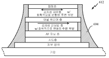
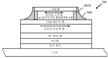
[0071] 도 5a는, 구성 층들의 확장 X-Y 면에 법선인 X-Z 투영면 상에서의 횡단면도이며, 이는 다른 예시적인 실시예에 따라 구조화되고 그리고 이에 따라 형성된 하나의 예시적인 화학적으로 변형된 엣지("CME") 멀티-층 MTJ 디바이스(500)의 양상들을 도시한다. 일 양상에서, CME 멀티-층 MTJ 디바이스(500)는, 보호층(502)과 추가로 조합되는 CME 멀티-층 MTJ 디바이스(400)를 포함할 수 있다. 이 양상에 추가로, 보호층(502)은, CME 강자성 피닝된 층(460)의 화학적으로 변형된 주변 부분(4604) 위에 그리고 CME 강자성 자유층(462)의 화학적으로 변형된 주변 부분(4624) 위에 형성될 수 있다. 보호층(502)은, 예를 들어, AlOx로 형성될 수 있다.5A is a cross-sectional view on an XZ projection plane that is normal to the extended XY plane of the constituent layers, which is structured according to another exemplary embodiment and is formed by one exemplary chemically modified edge ("CME" Lt; RTI ID = 0.0 > MTJ < / RTI > In one aspect, the CME
[0072] 보호층(502)의 다양한 이점들은, 예를 들어, 화학적으로 변형된 주변 부분(4624 및/또는 4604)의 원치않는 이주 또는 하각작용(deepening)에 대한 보호를 포함할 수 있다. 보호층(502)의 다른 이점들은, 원치않는 약한 강자성 효과들을 재-삽입할 수 있는 화학적으로 변형된 주변 부분(4624 및/또는 4604)에 대한 화학적 손상 보호일 수 있다. 일 양상에서, 보호층(502)은 CME 강자성 자유층(462) 및 CME 강자성 피닝된 층(460) 각각의 화학적으로 변형된 주변 부분(4624 및 4604)을 형성하는 트랜스포메이션이 프로세싱된 직후에 형성될 수 있다.[0072] The various advantages of the
[0073] 도 6a-도 6c는, 하나 또는 그 초과의 예시적인 실시예들의 양상들에 따른 프로세스에서 형성된 중간 구조들일 수 있는 구조적 형성물들의 하나의 예시적인 시퀀스를 도시하며, 그 예시는 도 8을 참조하여 더욱 상세하게 설명된다. 도 6d는, 도 6a-도 6c의 예시적 시퀀스와 조합될 수 있는, 일 양상에 따른 하나의 예시적인 추가 시퀀스를 도시한다. 도 6e는, 도 6a-도 6c의 예시적 시퀀스와 조합될 수 있는, 일 양상에 따른 다른 추가 시퀀스의 일례를 도시한다. 도 6f는, 도 6a-도 6c 및 도 6e의 예시적 조합 시퀀스와 조합될 수 있는, 일 양상에 따른 또 다른 추가 시퀀스에 대한 일 예시를 도시한다.[0073] Figures 6A-6C illustrate one exemplary sequence of structural features that may be intermediate structures formed in a process according to one or more aspects of the exemplary embodiments, Will be described in more detail with reference to FIG. Figure 6d illustrates one exemplary additional sequence in accordance with an aspect, which may be combined with the example sequences of Figures 6a-6c. 6E shows an example of another additional sequence in accordance with an aspect, which may be combined with the example sequence of Figs. 6A-6C. 6F illustrates an example of another additional sequence according to an aspect, which may be combined with the example combination sequences of Figs. 6A-6C and 6E.
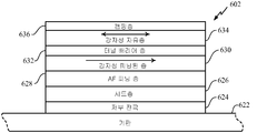
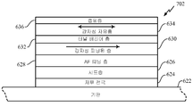
[0074] 도 6a를 참조하면, 예시적 MTJ 멀티-층 시작 구조(602)가, 형성 또는 제공될 수 있고, MTJ 기판(622)(이하, "기판"(622))에서 시작하여, 저부 전극(624), 시드층(626), AF 피닝 층(628), 강자성 피닝된 층(630), 터널 배리어 층(632), 강자성 자유층(634), 및 캡핑 층(636)의 그 도시된 스태킹 순서로 열거되어 있을 수 있다. 일 양상에서, 강자성 자유층(634)은 CoFeB, NiFe, 또는 CoFe, 또는 이들의 임의의 조합 또는 서브조합을 포함할 수 있다. 다른 양상에서, 강자성 피닝된 층(630)은 CoFeB, CoFe, 또는 둘 다를 포함할 수 있다. MTJ 기판(622), 저부 전극(624), 시드층(626), AF 피닝층(628), 터널 배리어 층(632), 및 캡핑 층(636)을 형성하는 재료와 관련하여, 이들은 종래의 MTJ 설계 기법들에 따를 수 있고, 이에 따라 추가의 상세 설명은 생략된다. MTJ 기판(622), 저부 전극(624), 시드층(626), AF 피닝층(628), 강자성 피닝된 층(630), 터널 배리어 층(632), 강자성 자유층(634) 및 캡핑 층(636)을 형성하기 위한 방법과 관련하여, 이들은 종래의 MTJ 제조 기법들에 따를 수 있고, 이에 따라 추가의 상세 설명은 생략된다.6A, an exemplary MTJ
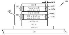
[0075] 도 6a를 여전히 참조하면, 하나의 예시적인 실시예에 따른 예시적 프로세스에서, 종래의 에칭은, 예를 들어, 인-프로세스 MTJ 필러(650)를 갖는 도 6b의 인-프로세스 구조(604)를 형성하기 위해 저부 전극 층(624)으로 하향하여 도 6a의 MTJ 멀티-층 시작 구조(602) 상에서 수행될 수 있다. 일 양상에서, 종래의 에칭은, 인-프로세스 MTJ 필러(650)가 화학적으로 손상된 주변 엣지 강자성 ("손상된 PEFM") 피닝된 층(660) 및 손상된 PEFM 자유층(662)을 포함하게 되는 방식으로, 인-프로세스 MTJ 필러(650)를 형성하는데 이용될 수 있다. 손상된 PEFM 피닝된 층(660)은 "인-프로세스 손상된 PEFM 피닝된 층"(660)으로 대안적으로 지칭될 수 있고, 손상된 PEFM 자유층(662)은 "인-프로세스 손상된 PEFM 자유층"(662)으로 대안적으로 지칭될 수 있다. 관련 양상에서, 인-프로세스 손상된 PEFM 자유층(662)은 화학적으로 손상된 주변 영역(6624) 및 메인 영역(6622)을 포함한다. 본 개시물에서 앞서 논의된 바와 같이, 화학적으로 손상된 주변 영역들(6604 및 6624)은 약한 강자성이 될 수 있어서, 디바이스 성능에 원치않는 영향들을 가질 수 있다.[0075] Still referring to FIG. 6A, in an exemplary process according to one exemplary embodiment, a conventional etch may be performed using the in-process structure (FIG. 6B) of FIG. 6B with, for example,
[0076] 도 6b를 참조하면, 도 3b의 깊이 DP의 방향에 비해 내측 방사상 방향에서 측정된 화학적으로 손상된 주변 영역(6624)의 깊이 DPT는, 종래의 에칭 조절 기법들을 이용하여, 당업자들에 의해 용이하게 조절될 수 있다. 일 양상에서, 손상된 PEFM 피닝된 층(660)의 화학적으로 손상된 주변 영역(6604)의 깊이(도시되지만 별도로 라벨링되지 않음)는 DPT와 동일하거나 또는 실질적으로 동일할 수 있다는 점이 가정될 수 있다.Referring to FIG. 6B, the depth DPT of the chemically damaged
[0077] 도 4a-도 4b를 참조하여 앞서 설명된 바와 같이, 다양한 예시적인 실시예들은, 도 6b를 참조하여, 메인 영역(6622)의 직경이 원하는 유효 MTJ 면적을 손상된 PEFM 자유층(662)에 제공하도록, 인-프로세스 MTJ 필러(650)의 (수평 폭으로 도시되지만, 별도로 라벨링되지 않은) 전체 직경을 선택하는 것을 포함할 수 있다. 원하는 유효 MTJ 영역은 또한 "타겟 MTJ 영역"으로 참조될 수 있다. 본 개시물의 당업자들에 의해 용이하게 인식되는 바와 같이, 이 양상의 관점에서 깊이 DPT는 조절될 수 있다.[0077] As described above with reference to FIGS. 4A-4B, various exemplary embodiments, with reference to FIG. 6B, show that the diameter of the
[0078] 도 6b를 참조하면, 손상된 PEFM 자유층(662) 및 손상된 PEFM 피닝된 층(660)의 화학적으로 손상된 주변 영역들(6624 및 6604)은 비록 약할지라도(즉, 메인 영역들(6622 및 6602)의 강자성 특성에 비해 현저하게 저하됨), 여전히 강자성 특성을 가질 수 있다. 화학적으로 손상된 주변 영역들(6624 및 6604)의 나머지 약한 강자성 특성에 대한 원인은, 이러한 영역들로 확산하는 O, N 및/또는 F로부터 초래된 손상에도 불구하고, 전체적인 또는 충분히 전체적인 산화, 질화, 또는 불화를 야기하기에는 확산이 불충분했다는 것이다. 그 결과는, 화학적으로 손상된 주변 영역들(6624 및 6604)이 현저하게 저하된 강자성 특성들, 예를 들어, 현저하게 감소된 강자성 교환 결합을 갖는다는 것이다. 이는, 결국, 최종 디바이스에서 현저하게 저하된 MTJ 스위칭 특성들을 초래할 수 있다. 다양한 예시적인 실시예들에 따른 프로세스들 및 장치들은, 다른 특징들 및 이점들 중에서도 특히, 개별적인 화학적으로 손상된 주변 영역(6604) 및/또는 화학적으로 손상된 주변 영역(6624)의 전체 또는 허용가능한 비율을 강자성 데드인 화학적 조성으로 트랜스포밍하는 트랜스포메이션 프로세스들을 수행함으로써 이러한 저하 효과의 현저한 감소 또는 제거를 제공한다.6B, the chemically damaged
[0079] 도 6c는, 하나 또는 그 초과의 예시적인 실시예들에 따라서, 도 6b의 인-프로세스 구조(604)와 같은 구조들에 대한 트랜스포메이션 프로세스에 의해 제공될 수 있는 디바이스(606)를 도시한다. 트랜스포메이션은, 산화, 질화, 또는 불화, 또는 이들의 임의의 조합 또는 서브-조합을 포함할 수 있다. 일 양상에서, 트랜스포메이션 프로세스는 손상된 PEFM 피닝된 층(660)의 개별적인 화학적으로 손상된 주변 영역(6604)의 실질적으로 전부를 강자성 데드인 화학적으로 변형된 주변 부분(6804)으로 변환 또는 트랜스포밍할 수 있다. 강자성 데드인 화학적으로 변형된 주변 부분(6804)은 메인 강자성 영역(6802)을 둘러싼다. 일 양상에서, 트랜스포밍은, 화학적으로 변형된 주변 부분(6804)과 메인 강자성 영역(6802) 사이에 약간의(만약 존재한다면) 나머지 또는 잔류하는 화학적으로 손상된 영역이 존재하도록, 수행될 수 있다. 일 양상에서, 화학적으로 변형된 주변 부분(6804)의 화학적 조성은, 예를 들어, FeOx, CoOx, CoFeOx, BOx, FeNx, CoNx, CoFeNx, BNx, FeFx, 및/또는 CoFx 또는 이러한 화학적 화합물들의 임의의 조합 또는 서브-조합을 포함할 수 있다.[0079] Figure 6c illustrates a
[0080] 도 6c를 여전히 참조하면, 하나의 또는 예시적인 실시예들에 따라, 트랜스포메이션 프로세스는 산화 프로세스를 포함할 수 있다. 이는 화학적으로 변형된 주변 부분(6804)에 FeOx, CoOx, CoFeOx, 및/또는 Box 중 하나 또는 그 초과 또는 이들의 임의의 조합 또는 서브-조합을 포함하는 화학적 조성을 제공할 수 있다. 다른 양상에서, 트랜스포메이션 프로세스는 FeNx, CoNx, CoFeNx 및/또는 BNx 중 하나 또는 이들의 하나 또는 그 초과의 조합을 갖는 화학적 조성을 화학적으로 변형된 주변 부분(6804)에 제공하는 질화 프로세스를 포함할 수 있다. 추가적인 양상에서, 트랜스포메이션 프로세스는, FeFx 및/또는 CoFx 중에서 하나 또는 그 초과를 갖는 화학적 조성을 화학적으로 변형된 주변 부분(6804)에 제공하는 불화 프로세스를 포함할 수 있다. 다른 양상에서, 자기 데드 화학적으로 변형된 주변 부분(6804)으로의 화학적으로 손상된 주변 영역(6604)의 트랜스포메이션은, 질화 프로세스, 산화 프로세스 및/또는 불화 프로세스 중 임의의 2개 또는 그 초과의 조합을 포함할 수 있다. 이는, 결국, 단독으로 동작하는 임의의 프로세스들에 의해 제공된 앞서-설명된 화학적 조성들의 다양한 조합들 및 서브-조합들을 갖는 화학적 조성을 화학적으로 변형된 주변 부분(6804)에 제공할 수 있다.[0080] Still referring to FIG. 6C, in accordance with one or the exemplary embodiments, the transformation process may include an oxidation process. This may provide a chemical composition comprising one or more of FeOx, CoOx, CoFeOx, and / or Box, or any combination or sub-combination thereof, in the chemically modified
[0081] 도 6c를 참조하면, 디바이스(606)는, 일 양상에 따라, 화학적으로 변형된 주변 부분(6804)의 깊이 DPM이 화학적으로 손상된 주변 영역(6624)의 도 6b의 깊이 DPT와 실질적으로 동일하게 되도록 조절된 그리고 적용된 트랜스포메이션을 도시한다. 하나 또는 그 초과의 예시적인 실시예들의 양상들에서, 산화, 질화 및/또는 불화 프로세스들은 (손상되지 않은) 메인 영역(6622) 상에서보다 화학적으로 손상된 주변 영역(6624) 상에서 더욱 빠르게 작용하는 양상들을 활용하도록 적용되고 구성된다. 이러한 양상들은, 예를 들어, 산화, 질화 및/또는 불화에 대한 프로세스 파라미터들, 예를 들어, 시간 및 환경의 더욱 용이한 설정의 이점들을 제공할 수 있다는 점이 인식될 것이다. 일 예시로서, 화학적으로 손상된 주변 영역(6624)의 허용가능한 트랜스포메이션을 제공하는 산화, 질화 및/또는 불화 파라미터들이, 도 6b의 메인 영역(6622)으로의 산화, 질화, 및/또는 불화의 허용불가한 이주 없이, 더욱 용이하게 설정될 수 있다.Referring to FIG. 6C, the
[0082] 도 6c의 디바이스(606)는, 하나 또는 그 초과의 예시적인 실시예들에 따른, 손상된 PEFM 피닝된 층(660)의 화학적으로 손상된 주변 영역(6604), 및 손상된 PEFM 자유층(662)의 화학적으로 손상된 주변 영역(6624) 둘 다의 트랜스포메이션들을 나타낸다. 트랜스포밍은, CME 강자성 피닝된 층(680) 및 CME 강자성 자유층(682)을 각각 형성한다. CME 강자성 피닝된 층(680)은, 손상된 PEFM 피닝된 층(660)의 화학적으로 손상된 주변 영역(6604)을 화학적으로 변형된 주변 영역(6804)으로 트랜스포밍하는 것에서 초래된다. CME 강자성 자유층(682)은, 손상된 PEFM 자유층(662)의 화학적으로 손상된 주변 영역(6624)을 화학적으로 변형된 주변 영역(6824)으로 트랜스포밍하는 것에서 초래된다. 이는, 일 양상이며, 예시적인 실시예들 중 임의의 것의 범위를 제한하는 것으로 의도되지 않는다. 예를 들어, 인-프로세스 MTJ 필러(650)를 형성했던 에칭 중 하나 또는 그 초과를 변경함으로써, 트랜스포메이션 프로세스는 손상된 PEFM 피닝된 층(660) 및 손상된 PEFM 자유층(662) 중 하나에 대해 선택적일 수 있다. 하나 또는 그 초과의 예시적인 실시예들에 따른 하나의 예시적 2-단계 에칭 및 복원 프로세스는 예를 들어 도 7a-도 7f를 참조하여 이후 더욱 상세하게 설명된다.[0082] The
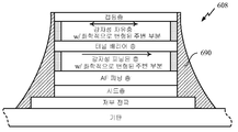
[0083] 도 6c를 참조하면, 디바이스(606)는, 일 양상에서, 하나 또는 그 초과의 예시적인 실시예들에 따른 완성된 디바이스일 수 있으며, 이 실시예들에 따라 완성된 프로세스들을 나타낼 수 있다. 다른 양상에서, 다양한 예시적인 실시예들은, 예를 들어, CME 강자성 피닝된 층(680)의 화학적으로 변형된 주변 부분(6804), 및 CME 강자성 자유층(68)의 화학적으로 변형된 주변 부분(6824) 중 하나 또는 그 초과 상에 보호층을 형성하는 것을 포함할 수 있다.[0083] Referring to Figure 6c, the
[0084] 도 6d는 이러한 예시적인 실시예들 중 하나 또는 그 초과에 따른 하나의 예시적 디바이스(608)의 단면도를 나타낸다. 도 6d의 디바이스(608)는 CME 강자성 피닝된 층(680) 및 CME 강자성 자유층(682)을 갖는 (도시되지만 별도로 넘버링되지 않은) 필러를 둘러싸는 보호층(690)을 갖는 도 6c의 디바이스(606)를 포함한다. 보호층은, 예를 들어, AlOx로 형성될 수 있다. 이러한 양상의 하나의 예시적인 이점은, 보호층(690)이 화학적으로 변형된 주변 영역들(6804 및 6824)을 후속 손상으로부터 보호하는 것일 수 있다.[0084] FIG. 6D shows a cross-sectional view of one
[0085] 도 6a-도 6d에 도시된 예시적인 실시예들은, 트랜스포메이션 양상들, 예를 들어, 산화, 질화 및/또는 불화에 의해 형성된 화학적으로 변형된 주변 영역들을 유지하는 것으로서 설명되어 있다. 다른 양상에서, 예시적인 실시예들은, 화학적으로 변형된 주변 영역의 전체 또는 선택된 부분을 제거하는 것을 포함할 수 있다. 제거는, 예를 들어, 트림 또는 이온 밀링에 의해 수행될 수 있다.[0085] The exemplary embodiments shown in FIGS. 6A-6D are described as maintaining chemically modified peripheral regions formed by the transformational aspects, eg, oxidation, nitridation, and / or fluorination. In another aspect, exemplary embodiments can include removing all or selected portions of the chemically modified peripheral region. Removal can be performed, for example, by trim or ion milling.
[0086] 도 6e는, 화학적으로 변형된 주변 영역의 전체 또는 선택된 부분의 이러한 제거를 포함하는 하나 또는 그 초과의 예시적인 실시예들에 따른 프로세스들에 따라, 그리고 이들로부터 초래되는 예시적 구조를 갖는 하나의 디바이스(610)를 도시한다. 도 6e의 디바이스(610)는, 편의를 위해, 도 6c의 디바이스(606) 상에서 수행된 후속 트림 또는 이온 밀링 프로세스들로부터 초래된 것으로 도시된다. 도 6e의 디바이스(610)는, 후속 트림 또는 이온 밀링이 "손상되지 않은 주변 영역" 또는 명료하게는 "손상되지 않은" 강자성 자유층(692)으로 명명되는 것을 형성하기 위해 도 6c의 CME 강자성 자유층(682)의 화학적으로 변형된 주변 영역(6824)을 제거하는 것을 도시한다. 용어 "손상되지 않은 주변" 강자성 자유층(692)에서의 용어 "손상되지 않은"은, 강자성 메인 영역에 비해 자신의 바깥쪽 주변에, 잔여물, 즉, 0이 아닌 실제 손상을 갖지만, 허용가능하게 낮은 강자성 특성들을 나타내는 구조를 포괄하는 것으로 이해될 것이다.[0086] Figure 6e illustrates an exemplary structure resulting from and derived from processes according to one or more exemplary embodiments that include such removal of all or selected portions of a chemically modified peripheral region Lt; RTI ID = 0.0 > 610 < / RTI > The
[0087] 도 6e를 참조하면, 예시적 디바이스(610)는, CME 강자성 피닝된 층(680)의 화학적으로 변형된 주변 영역(6804)을 남겨두면서, 오직 화학적으로 변형된 주변 영역(6824)만의 트리밍 또는 이온 밀링을 도시한다. 이는, 오직 예시적 목적을 위해서이며, 임의의 예시적인 실시예에 따른 프랙티스들의 범위를 제한하는 것으로 의도되지 않는다는 점이 이해될 것이다. 예를 들어, 하나 또는 그 초과의 예시적인 실시예들에 따른 (도면들에는 도시되지 않은) 추가 트림 또는 이온 밀링 동작은 CME 강자성 피닝된 층(680)의 화학적으로 변형된 주변 영역(6804)을 제거할수 있다.6E, an
[0088] 도 6f는 하나 또는 그 초과의 예시적인 실시예들에 따라 그리고 이들에 따른 프로세스로부터 초래되는 예시적 구조를 갖는 일 디바이스(612)를 도시한다. 디바이스(612)는, 하나 또는 그 초과의 화학적으로 변형된 주변 영역들의 전부 또는 선택된 부분의 제거에 더해, 보호층(694)을 포함한다. 보호층은, 도 6e의 손상되지 않은 강자성 자유층(692)의 (도시되지만 별도로 라벨링되지 않은) 주변을, 그리고 추가적인 양상에서는, CME 강자성 피닝된 층(680)의 화학적으로 변형된 주변 부분(6804)을 커버하도록 형성된다.[0088] Figure 6f illustrates a
[0089] 도 7a 내지 도 7f는, 하나 또는 그 초과의 예시적인 실시예들에 따라 2-단계 에칭 및 복원 프로세스로 형성된 구조들의 예시적 스냅샷들을 도시한다. 양상들, 특히, 2-단계 에칭 및 복원 프로세스에 포커싱되도록 지원하기 위해, 구조들의 예시적 동작들 및 예시적 스냅샷들은 도 6a-도 6f를 참조하여 설명된 특정 동작들 및 특정 구조들의 변형으로서 제시 및 설명된다.[0089] Figures 7A-7F illustrate exemplary snapshots of structures formed with a two-step etch and repair process in accordance with one or more exemplary embodiments. To assist in focusing on the aspects, particularly the two-step etch and restoration process, exemplary operations and illustrative snapshots of structures are shown as variations of certain operations and specific structures described with reference to FIGS. 6A-6F Presented and explained.
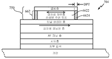
[0090] 도 7a를 참조하면, 하나의 예시적 프로세스는 이전에 설명된 도 6a의 MTJ 멀티-층 시작 구조(602)와 동일할 수 있는 MTJ 멀티-층 시작 구조(702)로 시작할 수 있다. 하나의 예시적인 실시예에 따른 하나의 예시적 프로세스에서, 종래의 에칭 기법들에 따를 수 있는 제 1 에칭이 인-프로세스 필러(750)를 갖는 인-프로세스 구조(704)를 형성하기 위해 도 7a의 MTJ 멀티-층 시작 구조(702) 상에서 수행될 수 있다. 인-프로세스 필러(750)는, 이전에 설명된 손상된 PEFM 자유층(662)을 인-프로세스 강자성 층으로서 포함할 수 있다. 일 양상에서, 손상된 PEFM 자유층(662)은, 이전에 설명된 바와 같이 강자성인 메인 영역(6622), 및 화학적으로 손상된 주변 영역(6624)을 포함할 수 있다. 화학적으로 손상된 주변 영역(6624)은 이전에 설명된 깊이 DPT를 가질 수 있다. 인-프로세스 필러(750)의 (수평 폭으로서 도시되지만, 별도로 라벨링되지 않은) 전체 직경은, 이전에 설명된 바와 같이, 메인 영역(6622)에 원하는 유효 또는 타겟 MTJ 면적을 제공한다. 손상된 PEFM 자유층(662)의 화학적으로 손상된 주변 영역(6624)은, 이전에 설명된 바와 같이, 약한 강자성 특성을 가질 수 있는데, 즉, 메인 영역들(6622 및 6602)의 강자성 특성에 비해 현저하게 저하될 수 있다.[0090] Referring to FIG. 7A, one exemplary process may begin with an MTJ
[0091] 도 7c는, 도 7b의 인-프로세스 구조(704)와 같은 구조들 상에서, 하나 또는 그 초과의 예시적인 실시예들에 따른, 트랜스포메이션 프로세스로부터 제공될 수 있는 화학적으로 변형된 엣지, 또는 CME 강자성 자유층(682)을 갖는 디바이스(706)를 도시한다. 자신의 CME 강자성 자유층(682)을 갖는 도 7c의 디바이스(706)는 산화, 질화 및/또는 불화 중 임의의 하나 또는 이들의 조합을 사용하는 트랜스포밍에 의해 제공될 수 있다. 일 양상에서, 메인 영역(6822)을 둘러싸는 화학적으로 변형된 주변 영역(6824)을 갖는 도 7c의 CME 강자성 자유층을 형성하기 위해 도 7b의 손상된 PEFM 자유층(662)의 각각의 화학적으로 손상된 주변 영역(6624)의 실질적으로 전체를 트랜스포밍하는 트랜스포밍이 (예를 들어, 시간 지속기간을 가지고) 수행될 수 있다. 이전에 설명된 바와 같이, 화학적으로 변형된 주변 영역(6824)은 FeOx, NiFeOx, CoOx, CoFeOx, BOx, FeNx, NiFeOx, CoNx, CoFeNx, BNx, FeFx, NiFeFx, CoFx, CoFeFx 및/또는 BFx, 또는 이러한 화학적 화합물들의 임의의 조합 또는 서브-조합을 포함할 수 있다. 화학적으로 변형된 주변 영역(6824)의 화학적 조성은, 일 양상에 따라, 강자성 데드일 수 있다.[0091] FIG. 7C illustrates, on structures such as the in-
[0092] 도 7d는, 일 양상에서, 도 7c를 참조하여 설명된 바와 같이 형성된 화학적으로 변형된 주변 영역(6824)을 포함하는 표면들 상에, 예를 들어, 이 표면들을 둘러싸게 형성될 수 있는 보호층(760)을 갖는 인-프로세스 디바이스(708)를 도시한다. 보호층은, 예를 들어, AlOx로 형성될 수 있다. 다음으로, 도 7e에 도시된 바와 같이, 예를 들어, 인-프로세스 구조(710)를 형성하기 위해 기판(622)으로 하향하여 연장하는 다른 또는 제 2 에칭이 수행될 수 있다. 일 양상에서, 도 7e의 인-프로세스 구조(710)를 초래하는 에칭은, 다른 또는 제 2 인-프로세스 강자성 층(762)으로서 강자성 피닝된 층(630)의 일부를 포함시키기 위해 인-프로세스 필러(750)의 바닥 또는 베이스(base)를 하강시키는데, 즉, 이들을 연장시킨다.[0092] Figure 7d, in one aspect, may be formed on surfaces including the chemically modified
[0093] 제 2 인-프로세스 자기층(762)은, 이 예시에서, 인-프로세스 강자성 피닝된 층이다. 그렇지만, 에칭이 제 2 강자성 메인 영역을 둘러싸는 제 2 화학적으로 손상된 주변 엣지 영역을 갖는 제 2 인-프로세스 강자성 층을 형성하는 제 2 에칭의 일례일 수 있다. 인-프로세스 강자성 피닝된 층(762)인 제 2 인-프로세스 강자성 층의 특정 예시에서, 화학적으로 손상된 주변 엣지 영역(7622)은 강자성 메인 영역(7624)을 둘러싼다.[0093] The second in-process
[0094] 도 7d 및 도 7e를 참조하면, 보호층(760)의 이점들 및 특징들은, 예를 들어, 도 7e의 인-프로세스 구조(710)를 형성하는 에칭으로부터 발생하는 손상으로부터 화학적으로 변형된 주변 부분(6824)을 보호하는 것을 포함할 수 있다는 점이 인식될 것이다. 유사하게, 보호층(760)이 강자성 메인 영역(6822)을 손상으로부터 보호하는 것으로 인식될 것이다.7D and 7E, the advantages and features of the
[0095] 도 7e에 도시된 에칭의 깊이는 오직 예시적 목적들을 위한 것임이 이해될 것이다. 에칭은, 예를 들어, 시드층(626)에서, 또는 다른 예시로서는, 저부 전극(624)에서 중지될 수 있다. 다른 대안에서, 도 7d에서의 에칭은, 예를 들어, 시드층(626)으로 계속할 수 있고, 그후 제 3 에칭이 수행될 수 있다.[0095] It will be appreciated that the depth of the etch shown in Figure 7e is for illustrative purposes only. The etch may be stopped, for example, in the
[0096] 도 7e를 참조하면, 앞서 설명된 바와 같이, 인-프로세스 강자성 피닝된 층(762)은 화학적으로 손상된 주변 엣지 영역(7622) 및 강자성 메인 영역(7624)을 갖는다. 일 양상에서, 화학적으로 손상된 주변 엣지 영역(7622) 상에 임의의 방해 구조를 적용 또는 형성하기 전에, 화학적으로 손상된 주변 엣지 영역(7622)의 전체, 또는 허용가능한 비율 또는 부분을 화학적으로 변형된 주변 부분으로 트랜스포밍하기 위해 트랜스포밍이 수행될 수 있다. 추가적인 양상에서, 그후 그 화학적으로 변형된 주변 부분 위에 다른 보호층이 형성될 수 있다. 도 7f는, 화학적으로 변형된 주변 부분(764), 및 다른 보호층(766)을 가지며, 다른 보호층의 앞서 설명된 트랜스포밍 및 형성을 나타내는 예시적 구조(712)를 도시한다.[0096] Referring to FIG. 7E, as described above, the in-process ferromagnetic pinned
[0097] 도 8은, 하나 또는 그 초과의 예시적인 실시예들에 따른 MTJ 디바이스들의 층들의 엣지-복원 및 엣지-보호의 다양한 양상들에 대한 추가적인 하나의 프로세스(800)의 하나의 플로우차트 도면을 도시한다.[0097] FIG. 8 is a flow chart diagram of an additional one
[0098] 도 8을 참조하면, 프로세스(800)의 또는 이에 대한 추가적인 하나의 예시적인 동작은, 802에서, MTJ 디바이스들이 에칭될 수 있는 도 6a의 MTJ 멀티-층 시작 구조(602), 또는 임의의 다른 멀티-층 시작 구조와 같은 멀티-층 MTJ 시작 구조를 제공하거나 또는 형성하는 것으로 시작할 수 있다. 일 양상에서, 802에서 형성되거나 또는 제공된 MTJ 시작 구조는, CoFeB 또는 CoFe로 형성된 도 6a의 시작 구조 강자성 자유층(634)과 같은 적어도 하나의 강자성 층을 포함할 수 있다.[0098] Referring to Figure 8, a further exemplary operation of the
[0099] 도 8을 여전히 참조하면, 프로세스(800)의 또는 이에 대한 추가적인 하나의 예시적인 동작에서, 802에서 멀티-층 MTJ 시작 구조를 제공하거나 또는 형성한 후, 804에서, 적어도 하나의 인-프로세스 강자성 층을 갖는 적어도 중간 MTJ 구조를 획득하기 위해 적어도 하나의 강자성 층에 대한 종래의 에칭이 수행될 수 있다. 804에서의 종래의 에칭은, 손상된 PEFM 자유층(662)의 도 6b의 화학적으로 손상된 주변 영역(6624)과 같은 화학적으로 손상된 주변 영역을 갖는 적어도 하나의 인-프로세스 강자성 층을 형성하도록 구성될 수 있다. 일 양상에서, 804에서의 에칭은, 도 6b의 멀티-층 인-프로세스 MTJ 필러(650)와 같은 2개 또는 그 초과의 인-프로세스 강자성 층들의 스택을 갖는 MTJ 필러를 형성할 수 있다. 이전에 설명된 바와 같이, 도 6b의 인-프로세스 MTJ 필러(650)는, 인-프로세스 손상된 PEFM 피닝된 층(660), 터널 배리어 층(632), 및 인-프로세스 손상된 PEFM 자유층(662)을 포함한다. 다른 양상에서, 804에서의 에칭은, 자기 터널 정션 층들에 대하여, 오직 인-프로세스 손상된 PEFM 자유층(662)만을 갖는 도 7b의 인-프로세스 MTJ 필러(750)와 같은 MTJ 필러를 형성하는 제 1 에칭일 수 있다.[0099] Still referring to FIG. 8, after providing or forming a multi-layer MTJ start structure at 802, in a further exemplary operation of or in the
[00100] 도 8을 여전히 참조하면, 프로세스(800)의 하나의 예시적인 동작에서, 하나 또는 그 초과의 인-프로세스 손상된 엣지 강자성 층들을 생성하기 위해, 804에서의 에칭 이후에, 806에서, 하나 또는 그 초과의 예시적인 실시예들에 따른 트랜스포메이션 프로세스가 수행될 수 있다. 806에서의 트랜스포메이션 동작들은, 804에서 형성된 인-프로세스 강자성 층들의 화학적으로 손상된 주변 영역의 전부 또는 선택된 허용가능한 비율을 자기 데드 화학적으로 변형된 주변 부분으로 트랜스포밍하기 위해 적용(예를 들어, 시간 지속기간을 가짐)될 수 있다. 일 양상에서, 806에서의 트랜스포메이션 동작들은, 앞서 설명된 바와 같이, 산화(862), 질화(864) 및/또는 불화(866), 또는 이들의 임의의 조합 또는 서브-조합을 포함할 수 있다.[00100] Still referring to FIG. 8, in one exemplary operation of
[00101] 806에서의 트랜스포메이션 동작들은, 트랜스포밍될 화학적으로 손상된 주변 영역들 상에 방해 구조를 형성하기 전에 수행되어야만 하는 것으로 이해될 것이다. 본 개시물에서 앞서 설명된 바와 같이, 일 양상에서, 806에서의 트랜스포메이션 동작들은 강자성 층들의 손상되지 않은 부분들보다 현저하게 더 큰 레이트들로 산화, 질화, 및/또는 불화를 진행하는 강자성 층들의 화학적으로 손상된 주변 영역들의 사용을 활용 및 제공할 수 있다. 예시적인 실시예들에 따르면, 사용 및 활용은, 트랜스포메이션 프로세스 파라미터들, 예를 들어, 온도, 산화, 질화 및 불화 에이전트들 및 농도들을, 손상되지 않은 영역들의 허용불가한 트랜스포메이션 없이, 예를 들어, 화학적으로 손상된 주변 영역들의 만족스러운 트랜스포메이션, 즉, 화학적으로 변형된 주변 영역의 만족스러운 깊이가 획득될 수 있는 값들로 설정하는 것을 포함할 수 있다.[00101] It will be appreciated that the transformation operations at 806 must be performed before forming the disturbing structure on the chemically damaged peripheral regions to be transformed. As described above in this disclosure, in one aspect, the transformation operations at 806 are performed at a significantly higher rate than the intact portions of the ferromagnetic layers, and the ferromagnetic layers < RTI ID = 0.0 > Can utilize and provide the use of chemically damaged peripheral areas of the substrate. According to exemplary embodiments, use and utilization can be accomplished by transforming the transformation process parameters, e.g., temperature, oxidation, nitridation and fluoridation agents and concentrations, without unacceptable transformation of the intact areas, For example, it may include setting satisfactory transformations of chemically damaged peripheral regions, i.e., values at which a satisfactory depth of the chemically modified peripheral region can be obtained.
[00102] 도 8을 참조하면, 프로세스(800)의 또는 이에 대한 추가적인 하나의 예시적인 동작에서, 806에서의 트랜스포메이션 동작들 이후에, 812에서, 프로세스는 성공적으로 종결할 수 있다. 도 6c는, 자신의 디바이스(606)에 의해, 화학적으로 손상된 주변 영역들을, 만족스러운 깊이로, 그리고 화학적으로 변형된 주변 부분들로의 트랜스포메이션 이후에, 이러한 프로세스의 종결에 대한 하나의 예를 도시한다.[00102] Referring to FIG. 8, in one or more exemplary operations of
[00103] 다른 양상에서, 프로세스(800)의 하나의 예시적인 동작에서, 806에서의 트랜스포메이션 동작들 이후에, 프로세스는 808로 진행할 수 있고, 더욱 상세하게 이후 설명된 예시들에서, 806에서 형성된 모든 화학적으로 변형된 주변 부분들의 전체 또는 허용가능한 부분을 제거하기 위해 트림 또는 이온 밀링을 수행할 수 있다.[00103] In another aspect, in one exemplary operation of
[00104] 다른 양상에서, 프로세스(800)의 하나의 예시적인 동작은, 806에서의 트랜스포메이션 동작들 이후에 바로, 810으로 진행할 수 있고, 그리고 806에서 형성된 화학적으로 변형된 주변 부분들 상에 보호층을 적용하거나 또는 형성할 수 있다. 도 6d를 참조하면, 보호층(690)을 갖는 디바이스(608)는 810에서의 보호층의 형성에 의해 고려되는 프로세스들에 대한 하나의 예시적인 결과를 도시한다. 앞서 설명된 바와 같이, 810에서 형성된 보호층은, 예를 들어, AlOx일 수 있다. 일 양상에서, 810에서의 보호층의 형성 이후에, 프로세스(800)는 812에서 성공적으로 종결할 수 있다. 다른 양상에서, 804에서의 에칭이, 피닝된 강자성 층을 아직 갖지 않고 도 7b의 인-프로세스 필러(750)과 같은 필러를 형성했던 제 1 (또는 다른 중간) 에칭이었다면, 프로세스(800)의 동작들은 804로 복귀할 수 있고 이전 에칭에서 도달되었던 것보다 더 큰 깊이까지의 다른 에칭을 수행할 수 있다. 810에서 형성된 보호층은 806에서 형성된 자유 강자성 층의 화학적으로 변형된 주변 부분을 보호할 수 있다는 점이 인식될 것이다. 일 양상에서, 인-프로세스 피닝된 강자성 층을 획득하기 위해 앞서-설명된 블록에서 다른 에칭을 수행한 후에, 블록 806은 인-프로세스 피닝된 강자성 층의 화학적으로 손상된 주변 엣지 영역을 복원하기 위해 반복될 수 있다. 또한, 810에서 형성된 보호층은 인-프로세스 피닝된 강자성 층의 화학적으로 손상된 주변 엣지 영역의 이러한 복원 동안 추가적인 산화, 질화 및/또는 불화로부터, 806에서 형성된 자유 강자성층의 화학적으로 변형된 주변 부분을 보호할 수 있다는 점이 인식될 것이다.In another aspect, one exemplary operation of the
[00105] 도 8을 참조하면, 이전에 설명된 바와 같이, 프로세스(800)의 하나의 예시적인 동작에서, 806에서의 트랜스포메이션 동작들 이후에, 프로세스는 808로 진행할 수 있고 그리고 806에서 형성된 화학적으로 변형된 주변 부분들의 전부 또는 선택된 부분들의 전부 또는 허용가능한 부분을 제거하기 위해 트림 또는 이온 밀링을 수행할 수 있다. CME 강자성 자유층(682)의 화학적으로 변형된 주변 영역(6824)을 제거하기 위해 도 6c의 디바이스(606)에서의 동작의 결과인 도 6e의 디바이스(610)는, 808에서의 트림 또는 이온 밀링에 따라 형성될 수 있는 하나의 예시적인 구조를 나타낸다.8, in one exemplary operation of
[00106] 일 양상에서, 앞서 설명된 바와 같이 808에서 트림 또는 이온 밀링을 수행한 이후에, 프로세스(800)에서의 동작들은 812에서 종결할 수 있다. 다른 양상에서, 앞서 설명된 바와 같이 808에서의 트림 또는 이온 밀링을 수행한 후, 프로세스(800)에서의 동작들은 810으로 진행할 수 있고 그리고 보호 코팅을 적용 또는 형성할 수 있으며, 앞서 설명된 바와 같이, 그후 812에서 성공적으로 종결할 수 있다. 보호 코팅(694)을 갖는 도 6e의 디바이스인 도 6f의 디바이스(612)는, 808에서 트림 또는 이온 밀링과 같은 시퀀스에 따라 형성될 수 있고 그후 810에서 보호층이 형성되는 하나의 예시적인 구조를 도시한다.[00106] In one aspect, after performing trim or ion milling at 808 as described above, operations at
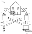
[00107] 도 9는, 본 개시물의 하나 또는 그 초과의 실시예들이 유리하게 채용될 수 있는 예시적인 무선 통신 시스템(900)을 예시한다. 예시적 목적들을 위해, 도 9는 3개의 원격 유닛들(920, 930, 및 950) 및 2개의 기지국들(940)을 도시한다. 종래의 무선 통신 시스템들이 수많은 그 이상의 원격 유닛들 및 기지국들을 가질 수 있다는 점이 인식될 것이다. 원격 유닛들(920, 930 및 950)은, 이하에 추가적으로 논의되는 것과 같은 본 개시물의 실시예들 중에서, 집적 회로 또는 (본원에 개시된 바와 같이, 온-칩 전압 레귤레이터들을 포함하는) 다른 반도체 디바이스들(925, 935 및 955)을 포함한다. 도 9는, 기지국들(940)로부터 원격 유닛들(920, 930 및 950)로의 순방향 링크 신호들(980)을, 그리고 원격 유닛들(920, 930 및 950)로부터 기지국들(940)로의 역방향 링크 신호들(990)을 나타낸다.[00107] FIG. 9 illustrates an exemplary
[00108] 도 9에서, 원격 유닛(920)은 이동 전화기로 도시되고, 원격 유닛(930)은 휴대용 컴퓨터로 도시되며, 원격 유닛(950)은 무선 로컬 루프 시스템 내의 고정형 위치 원격 유닛으로 도시된다. 예를 들어, 원격 유닛들(920, 930 및 950)은 모바일 전화기 또는 통신 디바이스, 핸드-헬드 개인 통신 시스템(PCS: personal communication systems) 유닛들, 개인용 디지털 보조기구 또는 PDA(personal data assistant)와 같은 휴대용 데이터 유닛, 내비게이션 디바이스(예컨대, GPS 인에이블 디바이스들), 셋 톱 박스, 음악 플레이어, 비디오 플레이어, 또는 다른 엔터테인먼트 유닛 중 임의의 하나 또는 조합일 수 있다. 이에 더해, 원격 유닛들(920, 930, 및 950)은 검침 장비(meter reading equipment)와 같은 임의의 고정형 위치 데이터 유닛, 또는 데이터 또는 컴퓨터 명령들을 저장 또는 리트리브하는 임의의 다른 디바이스, 또는 이들의 임의의 조합일 수 있다. 도 9가 원격 유닛들(920, 930 및 950)을 예시하지만, 다양한 예시적인 실시예들은 이러한 예시된 예시적 유닛들로 제한되지 않는 것으로 이해될 것이다. 본 개시물의 실시예들은 메모리를 포함하는 액티브 집적 회로 및 테스트 및 특징화를 위한 온-칩 회로를 포함하는 임의의 디바이스에 적합하게 채용될 수 있다.9,
[00109] (도 5a-도 5b의 디바이스들, 도 6a-도 6f에 의해 도시된 구조들의 시퀀스, 도 7의 방법들, 또는 이들의 임의의 조합과 같은) 앞서 개시된 디바이스들 및 기능들은, 컴퓨터 판독가능 유형 매체 또는 다른 컴퓨터 판독가능 매체에 저장된 컴퓨터 파일들(예를 들어, RTL, GDSII, GERBER, 등)으로 설계되고 구성될 수 있다. 일부 또는 전체의 이러한 파일들은, 이러한 파일들에 기초하여 디바이스들을 제조하는 제조 업자들에게 제공될 수 있다. 결과 제품들은, 이후에 반도체 다이로 절단되어 반도체 칩으로 패키징되는 반도체 웨이퍼들을 포함한다. 반도체 칩들은, 앞서 설명된 바와 같은 전자 디바이스들에 채용될 수 있다.The previously disclosed devices and functions (such as the devices of FIGS. 5A-5B, the sequence of structures depicted by FIGS. 6A-6F, the methods of FIG. 7, (E.g., RTL, GDSII, GERBER, etc.) stored in readable-type media or other computer-readable media. Some or all of these files may be provided to manufacturers who manufacture devices based on these files. The resulting products include semiconductor wafers which are subsequently cut into semiconductor dies and packaged into semiconductor chips. The semiconductor chips may be employed in electronic devices as described above.
[00110] 본원에 개시된 실시예들과 관련하여 설명된 방법들, 시퀀스들 및/또는 알고리즘들은 직접 하드웨어로 구현되거나, 프로세서에 의해 실행된 소프트웨어 모듈로 구현되거나, 또는 이 둘의 조합으로 구현될 수 있다. 소프트웨어 모듈은 RAM 메모리, 플래시 메모리, ROM 메모리, EPROM 메모리, EEPROM 메모리, 레지스터들, 하드 디스크, 탈착식 디스크, CD-ROM, 또는 당업계에 공지된 임의의 다른 형태의 저장 매체에 상주할 수 있다. 예시적인 저장 매체는, 프로세서가 저장 매체로부터 정보를 판독하고 저장 매체에 정보를 기록할 수 있도록, 프로세서에 커플링될 수 있다. 대안적으로, 저장 매체는 프로세서에 통합될 수 있다. [00110] The methods, sequences, and / or algorithms described in connection with the embodiments disclosed herein may be embodied directly in hardware, in a software module executed by a processor, or in a combination of the two have. The software module may reside in RAM memory, flash memory, ROM memory, EPROM memory, EEPROM memory, registers, a hard disk, a removable disk, a CD-ROM, or any other form of storage medium known in the art. An exemplary storage medium may be coupled to the processor such that the processor can read information from, and write information to, the storage medium. Alternatively, the storage medium may be integrated into the processor.
[00111] 이에 따라, 본 발명의 실시예는, 구현을 위한 방법을 채용하는 컴퓨터 판독가능 매체, 예를 들어, 컴퓨터 판독가능 유형 매체를 포함할 수 있다. 이에 따라, 본 발명은, 나타낸 예시들로 제한되지 않으며, 본원에 설명된 기능을 수행하기 위한 임의의 수단은 본 발명의 실시예들에 포함된다.[00111] Accordingly, embodiments of the present invention may include a computer readable medium, e.g., a computer readable medium, employing a method for implementation. Accordingly, the present invention is not intended to be limited to the examples shown, and any means for performing the functions described herein are included in the embodiments of the present invention.
[00112] 앞서 개시된 디바이스들 및 기능들은, 컴퓨터 판독가능 매체에 저장된 컴퓨터 파일들(예를 들어, RTL, GDSII, GERBER, 등) 로 설계되고 구성될 수 있다. 일부 또는 전체의 이러한 파일들은, 이러한 파일들에 기초하여 디바이스들을 제조하는 제조 업자들에게 제공될 수 있다. 결과 제품들은, 이후에 반도체 다이로 절단되어 반도체 칩으로 패키징되는 반도체 웨이퍼들을 포함한다. 이 칩들은, 그후 앞서 설명된 디바이스들에 채용될 수 있다.[00112] The previously disclosed devices and functions may be designed and configured with computer files (e.g., RTL, GDSII, GERBER, etc.) stored on a computer readable medium. Some or all of these files may be provided to manufacturers who manufacture devices based on these files. The resulting products include semiconductor wafers which are subsequently cut into semiconductor dies and packaged into semiconductor chips. These chips can then be employed in the devices described above.
[00113] 이전 개시물이 본 발명의 예시적인 실시예들을 나타내지만, 첨부된 청구항들에 의해 정의되는 본 발명의 범위로부터 벗어나지 않고 다양한 변화들 및 변형들이 본원에서 행해질 수 있다는 것에 주목해야 한다. 본원에 설명된 본 발명의 실시예들에 따른 방법 청구항들의 기능들, 단계들 및/또는 동작들은 임의의 특정한 순서로 수행될 필요는 없다. 게다가, 본 발명의 엘리먼트들은 단수표현으로 설명되거나 또는 청구될 수 있지만, 단수표현으로의 제한이 명확하게 언급되지 않는 한 복수표현도 고려된다.[00113] While the foregoing disclosure shows illustrative embodiments of the invention, it should be noted that various changes and modifications may be made herein without departing from the scope of the invention as defined by the appended claims. The functions, steps and / or operations of the method claims according to embodiments of the invention described herein need not be performed in any particular order. In addition, elements of the invention may be described or claimed in the singular, but multiple representations are contemplated unless limitation to the singular is explicitly stated.
Claims (42)
화학적으로 손상된 주변 영역에 의해 둘러싸인 강자성 메인 영역을 갖는 인-프로세스 강자성 층(in-process ferromagnetic layer)을 형성하는 단계 ― 상기 화학적으로 손상된 주변 영역은 약한 강자성임 ―; 및
상기 자기 터널 정션 층을 형성하기 위해 화학적으로 손상된 주변 영역의 적어도 일부를 화학적으로 변형된 주변 부분으로 트랜스포밍하는 단계를 포함하며,
상기 화학적으로 변형된 주변 부분은 비강자성(non-ferromagnetic)인,
자기 터널 정션 층을 형성하기 위한 방법.A method for forming a magnetic tunnel junction layer,
Forming an in-process ferromagnetic layer having a ferromagnetic main region surrounded by a chemically damaged peripheral region, the chemically damaged peripheral region being weakly ferromagnetic; And
Transforming at least a portion of the chemically damaged peripheral region to a chemically modified peripheral portion to form the magnetic tunnel junction layer,
The chemically modified peripheral portion is non-ferromagnetic,
A method for forming a magnetic tunnel junction layer.
상기 화학적으로 손상된 주변 영역의 적어도 일부를 화학적으로 변형된 주변 부분으로 트랜스포밍하는 단계는, 산화, 질화, 또는 불화 또는 이들의 임의의 조합을 포함하는,
자기 터널 정션 층을 형성하기 위한 방법.The method according to claim 1,
The step of transforming at least a portion of the chemically damaged peripheral region to a chemically modified peripheral portion comprises the steps of: oxidizing, nitriding, or fluorinating, or any combination thereof.
A method for forming a magnetic tunnel junction layer.
상기 자기 터널 정션 층에 대한 타겟 유효 면적을 식별하거나 또는 제공하는 단계를 더 포함하고,
상기 인-프로세스 강자성 층은 상기 타겟 유효 면적보다 더 큰 면적 치수를 갖고,
상기 트랜스포밍하는 단계는 강자성 메인 영역을 갖도록 상기 자기 터널 정션 층을 형성하는 단계를 포함하고,
상기 강자성 메인 영역은 상기 타겟 유효 면적과 대략적으로 동일한 면적을 갖는,
자기 터널 정션 층을 형성하기 위한 방법.The method according to claim 1,
Further comprising identifying or providing a target effective area for the magnetic tunnel junction layer,
Wherein the in-process ferromagnetic layer has an area dimension greater than the target effective area,
Wherein the transforming comprises forming the magnetic tunnel junction layer to have a ferromagnetic main region,
Wherein the ferromagnetic main region has an area approximately equal to the target effective area,
A method for forming a magnetic tunnel junction layer.
상기 인-프로세스 강자성 층은, NiFe, CoFeB, CoFe, 또는 B 중 임의의 것, 또는 이들의 임의의 조합 또는 서브-조합을 포함하는,
자기 터널 정션 층을 형성하기 위한 방법.The method according to claim 1,
The in-process ferromagnetic layer may comprise any of NiFe, CoFeB, CoFe, or B, or any combination or sub-combination thereof.
A method for forming a magnetic tunnel junction layer.
상기 화학적으로 변형된 주변 부분은 적어도 하나의 강자성 엘리먼트를 포함하는,
자기 터널 정션 층을 형성하기 위한 방법.The method according to claim 1,
Wherein the chemically modified peripheral portion comprises at least one ferromagnetic element.
A method for forming a magnetic tunnel junction layer.
상기 적어도 하나의 강자성 엘리먼트는 철, 니켈, 또는 코발트인,
자기 터널 정션 층을 형성하기 위한 방법.6. The method of claim 5,
Wherein the at least one ferromagnetic element is iron, nickel, or cobalt,
A method for forming a magnetic tunnel junction layer.
상기 화학적으로 변형된 주변 부분은, FeOx, CoOx, CoFeOx, BOx, FeNx, CoNx, CoFeNx, BNx, FeFx, CoFx, CoFeFx, 및/또는 BFx 중 임의의 것, 또는 이들의 임의의 조합 또는 서브-조합 또는 이들의 임의의 조합을 포함하는,
자기 터널 정션 층을 형성하기 위한 방법.6. The method of claim 5,
The chemically modified peripheral portion may be any of FeOx, CoOx, CoFeOx, BOx, FeNx, CoNx, CoFeNx, BNx, FeFx, CoFx, CoFeFx, and / or BFx, Or any combination thereof.
A method for forming a magnetic tunnel junction layer.
상기 화학적으로 변형된 주변 부분의 적어도 일부를 제거하는 단계를 더 포함하는,
자기 터널 정션 층을 형성하기 위한 방법.The method according to claim 1,
Further comprising removing at least a portion of the chemically modified peripheral portion.
A method for forming a magnetic tunnel junction layer.
상기 제거하는 단계는, 이온 밀링, 에칭, 또는 이온 밀링과 에칭의 조합을 포함하는,
자기 터널 정션 층을 형성하기 위한 방법.9. The method of claim 8,
Wherein the removing comprises ion milling, etching, or a combination of ion milling and etching.
A method for forming a magnetic tunnel junction layer.
상기 화학적으로 변형된 주변 부분을 둘러싸도록 보호층을 형성하는 단계를 더 포함하는,
자기 터널 정션 층을 형성하기 위한 방법.The method according to claim 1,
Further comprising forming a protective layer to surround the chemically modified peripheral portion,
A method for forming a magnetic tunnel junction layer.
상기 보호층은, 산화물 층, 질화물 층, 또는 산화물 층과 질화물 층의 조합인,
자기 터널 정션 층을 형성하기 위한 방법.11. The method of claim 10,
The protective layer may be an oxide layer, a nitride layer, or a combination of an oxide layer and a nitride layer.
A method for forming a magnetic tunnel junction layer.
상기 보호층은 AlOx을 포함하는,
자기 터널 정션 층을 형성하기 위한 방법.11. The method of claim 10,
Wherein the protective layer comprises AlOx.
A method for forming a magnetic tunnel junction layer.
상기 인-프로세스 강자성 층은 인-프로세스 강자성 자유층인,
자기 터널 정션 층을 형성하기 위한 방법.The method according to claim 1,
The in-process ferromagnetic layer is an in-process ferromagnetic free layer,
A method for forming a magnetic tunnel junction layer.
상기 인-프로세스 강자성 층은, 인-프로세스 강자성 피닝된 층인,
자기 터널 정션 층을 형성하기 위한 방법.The method according to claim 1,
The in-process ferromagnetic layer is an in-process ferromagnetic pinned layer,
A method for forming a magnetic tunnel junction layer.
상기 인-프로세스 강자성 층은, 제 1 인-프로세스 면적 치수를 갖는 제 1 인-프로세스 강자성 층이고,
상기 화학적으로 손상된 주변 영역은 제 1 화학적으로 손상된 주변 영역이고,
상기 인-프로세스 강자성 층을 형성하는 단계는,
상기 제 1 인-프로세스 강자성 층,
제 2 인-프로세스 강자성 층, 및
상기 제 1 인-프로세스 강자성 층과 상기 제 2 인-프로세스 강자성 층 사이의 터널 배리어 층
을 갖는 필러를 형성하는 단계를 포함하고,
상기 제 2 인-프로세스 강자성 층은 상기 제 1 인-프로세스 면적 치수보다 큰 제 2 인-프로세스 면적 치수를 갖고,
상기 제 2 인-프로세스 강자성 층은 제 2 화학적으로 손상된 주변 영역을 갖는,
자기 터널 정션 층을 형성하기 위한 방법.The method according to claim 1,
The in-process ferromagnetic layer is a first in-process ferromagnetic layer having a first in-process area dimension,
Wherein the chemically damaged peripheral region is a first chemically damaged peripheral region,
Wherein forming the in-process ferromagnetic layer comprises:
The first in-process ferromagnetic layer,
A second in-process ferromagnetic layer, and
And a tunnel barrier layer between the first in-process ferromagnetic layer and the second in-
≪ / RTI > forming a filler having a &
Wherein the second in-process ferromagnetic layer has a second in-process area dimension greater than the first in-process area dimension,
Said second in-process ferromagnetic layer having a second chemically damaged peripheral region,
A method for forming a magnetic tunnel junction layer.
상기 제 1 인-프로세스 강자성 층은 인-프로세스 강자성 자유층이고,
자기 터널 정션 층을 형성하기 위한 방법.16. The method of claim 15,
The first in-process ferromagnetic layer is an in-process ferromagnetic free layer,
A method for forming a magnetic tunnel junction layer.
상기 제 2 인-프로세스 강자성 층은 인-프로세스 강자성 피닝된 층인,
자기 터널 정션 층을 형성하기 위한 방법.17. The method of claim 16,
The second in-process ferromagnetic layer is an in-process ferromagnetic pinned layer,
A method for forming a magnetic tunnel junction layer.
기판, 상기 기판 위의 피닝된 강자성 층, 상기 피닝된 강자성 층 위의 터널 배리어 층, 및 상기 터널 배리어 층 위의 강자성 자유층을 포함하는 멀티-층 구조를 제공하는 단계;
필러(pillar)를 형성하기 위해 상기 멀티-층 구조를 에칭하는 단계 ― 상기 필러는 상기 강자성 자유층의 일부를 갖는 인-프로세스 강자성 층을 포함하고, 상기 인-프로세스 강자성 층은 강자성 메인 영역 및 상기 강자성 메인 영역을 둘러싸는 화학적으로 손상된 주변 영역을 포함하며, 상기 화학적으로 손상된 주변 영역은 약한 강자성임 ―; 및
상기 화학적으로 손상된 주변 영역의 적어도 일부를 화학적으로 변형된 주변 부분으로 트랜스포밍하는(transforming) 단계 ― 상기 화학적으로 변형된 주변 부분은 강자성 데드(ferromagnetic dead)임 ― 를 포함하는,
자기 터널 정션 디바이스를 제조하기 위한 방법.1. A method for fabricating a magnetic tunnel junction device,
Providing a multi-layer structure comprising a substrate, a pinned ferromagnetic layer on the substrate, a tunnel barrier layer on the pinned ferromagnetic layer, and a ferromagnetic free layer on the tunnel barrier layer;
Layer structure to form a pillar, the filler comprising an in-process ferromagnetic layer having a portion of the ferromagnetic free layer, the in-process ferromagnetic layer comprising a ferromagnetic main region and a ferromagnetic free layer, A chemically damaged peripheral region surrounding the ferromagnetic main region, wherein the chemically damaged peripheral region is weakly ferromagnetic; And
Transforming at least a portion of said chemically damaged peripheral region into a chemically modified peripheral portion, said chemically modified peripheral portion being ferromagnetic dead;
A method for fabricating a magnetic tunnel junction device.
상기 방법은:
상기 화학적으로 변형된 주변 부분을 둘러싸도록 보호층을 형성하는 단계; 및
추가로 상기 필러가 다른 인-프로세스 강자성 층을 포함하게 형성하기 위해 다른 에칭을 수행하는 단계를 더 포함하며,
상기 다른 인-프로세스 강자성 층은 상기 피닝된 강자성 층의 일부를 가지는,
자기 터널 정션 디바이스를 제조하기 위한 방법.19. The method of claim 18,
The method comprising:
Forming a protective layer to surround the chemically modified peripheral portion; And
Further comprising performing another etch to form the filler to include another in-process ferromagnetic layer,
Said other in-process ferromagnetic layer having a portion of said pinned ferromagnetic layer,
A method for fabricating a magnetic tunnel junction device.
상기 보호층은, 산화물 층, 질화물 층, 또는 산화물 층과 질화물 층의 조합인,
자기 터널 정션 디바이스를 제조하기 위한 방법.20. The method of claim 19,
The protective layer may be an oxide layer, a nitride layer, or a combination of an oxide layer and a nitride layer.
A method for fabricating a magnetic tunnel junction device.
상기 다른 인-프로세스 강자상 층은, 다른 강자성 메인 영역 및 상기 다른 강자성 메인 영역을 둘러싸는 다른 화학적으로 손상된 주변 영역을 포함하는 강자성 피닝된 층이고, 상기 다른 화학적으로 손상된 주변 영역은 약한 강자성이며,
상기 방법은:
상기 다른 화학적으로 손상된 주변 영역의 적어도 일부를 다른 화학적으로 변형된 주변 부분으로 트랜스포밍하는 단계를 더 포함하고,
상기 다른 화학적으로 변형된 주변 부분은 강자성 데드인,
자기 터널 정션 디바이스를 제조하기 위한 방법.20. The method of claim 19,
Wherein said another in-process ferromagnetic layer is a ferromagnetic pinned layer comprising another ferromagnetic main region and another chemically damaged peripheral region surrounding said another ferromagnetic main region, said other chemically damaged peripheral region being weakly ferromagnetic,
The method comprising:
Further comprising transforming at least a portion of said other chemically damaged peripheral region to another chemically modified peripheral portion,
The other chemically modified peripheral portion is a ferromagnetic dead,
A method for fabricating a magnetic tunnel junction device.
상기 방법은:
상기 다른 화학적으로 변형된 주변 부분을 둘러싸도록 보호층을 형성하는 단계를 더 포함하는,
자기 터널 정션 디바이스를 제조하기 위한 방법.The method of claim 21, wherein
The method comprising:
Further comprising forming a protective layer to surround said other chemically modified peripheral portion,
A method for fabricating a magnetic tunnel junction device.
상기 강자성 자유층은 상기 멀티-층 구조 내에서 제 1 깊이에 위치되고, 상기 피닝된 강자성 층은 상기 제 1 깊이보다 더 깊은 제 2 깊이에 위치되며, 상기 에칭은 제 1 에칭이고, 상기 제 1 에칭은 상기 제 1 깊이보다 더 깊고 상기 제 2 깊이 미만인 깊이까지에 대한 것이며, 상기 방법은:
상기 화학적으로 변형된 주변 부분을 둘러싸도록 보호층을 형성하는 단계; 및
추가로 상기 필러가 제 2 인-프로세스 강자성 층을 포함하게 형성하기 위해 상기 제 2 깊이보다 더 깊은 깊이까지의 제 2 에칭 단계를 더 포함하고,
상기 제 2 인-프로세스 강자성 층은 상기 피닝된 강자성 층의 일부를 갖는,
자기 터널 정션 디바이스를 제조하기 위한 방법.19. The method of claim 18,
Wherein the ferromagnetic free layer is located at a first depth within the multi-layer structure, the pinned ferromagnetic layer is located at a second depth deeper than the first depth, the etch is a first etch, The etch is for a depth deeper than the first depth and less than the second depth, the method comprising:
Forming a protective layer to surround the chemically modified peripheral portion; And
Further comprising a second etch step to a depth deeper than said second depth to form said filler to comprise a second in-process ferromagnetic layer,
Said second in-process ferromagnetic layer having a portion of said pinned ferromagnetic layer,
A method for fabricating a magnetic tunnel junction device.
상기 보호층은, 산화물 층, 질화물 층, 또는 산화물 층과 질화물 층의 조합인,
자기 터널 정션 디바이스를 제조하기 위한 방법.24. The method of claim 23,
The protective layer may be an oxide layer, a nitride layer, or a combination of an oxide layer and a nitride layer.
A method for fabricating a magnetic tunnel junction device.
상기 제 2 인-프로세스 강자성 층은 제 2 강자성 메인 영역 및 상기 제 2 강자성 메인 영역을 둘러싸는 제 2 화학적으로 손상된 주변 영역을 갖는 인-프로세스 피닝된 강자성 층이고, 상기 제 2 화학적으로 손상된 주변 영역은 약한 강자성이며, 상기 방법은:
상기 제 2 화학적으로 손상된 영역의 적어도 일부를 제 2 화학적으로 변형된 주변 부분으로 트랜스포밍하는 단계를 더 포함하고,
상기 제 2 화학적으로 변형된 주변 부분은 강자성 데드인,
자기 터널 정션 디바이스를 제조하기 위한 방법.24. The method of claim 23,
Wherein the second in-process ferromagnetic layer is an in-process pinned ferromagnetic layer having a second ferromagnetic main region and a second chemically damaged peripheral region surrounding the second ferromagnetic main region, the second chemically damaged peripheral region Is weak ferromagnetic, the method comprising:
Further comprising transforming at least a portion of the second chemically damaged region to a second chemically modified peripheral portion,
Wherein the second chemically modified peripheral portion is a ferromagnetic dead,
A method for fabricating a magnetic tunnel junction device.
상기 방법은:
상기 제 2 화학적으로 변형된 주변 부분을 둘러싸도록 다른 보호층을 형성하는 단계를 더 포함하는,
자기 터널 정션 디바이스를 제조하기 위한 방법.26. The method of claim 25,
The method comprising:
Further comprising forming another protective layer to surround said second chemically modified peripheral portion,
A method for fabricating a magnetic tunnel junction device.
타겟 유효 MTJ 면적보다 더 큰 인-프로세스 면적 치수를 갖는 인-프로세스 자기층을 형성하는 단계 ― 상기 형성하는 단계는, 상기 인-프로세스 자기층의 주변부에 화학적으로 손상된 영역을 형성하는 단계 ―; 및
상기 화학적으로 손상된 영역의 적어도 일부를 화학적으로 변형된 주변 부분으로 트랜스포밍하는 단계를 포함하고,
상기 화학적으로 변형된 주변 부분은 비강자성인,
자기 터널 정션(MTJ) 층을 형성하기 위한 방법.1. A method for forming a magnetic tunnel junction (MTJ) layer,
Forming an in-process magnetic layer having an in-process area dimension greater than the target effective MTJ area, the forming comprising: forming a chemically damaged region in the periphery of the in-process magnetic layer; And
Transforming at least a portion of the chemically damaged region to a chemically modified peripheral portion,
Wherein the chemically modified peripheral portion is non-ferromagnetic,
A method for forming a magnetic tunnel junction (MTJ) layer.
상기 화학적으로 변형된 주변 부분을 둘러싸도록 보호층을 형성하는 단계를 더 포함하는,
자기 터널 정션(MTJ) 층을 형성하기 위한 방법.28. The method of claim 27,
Further comprising forming a protective layer to surround the chemically modified peripheral portion,
A method for forming a magnetic tunnel junction (MTJ) layer.
기판, 상기 기판 위의 피닝된 강자성 층, 상기 피닝된 강자성 층 위의 터널 배리어 층, 및 상기 터널 배리어 층 위의 강자성 자유층을 포함하는 멀티-층 구조를 제공하는 단계;
필러를 형성하기 위해 상기 멀티-층 구조를 에칭하는 단계 ― 상기 필러는 상기 강자성 자유층의 일부를 갖는 인-프로세스 강자성 층을 포함하고, 상기 인-프로세스 강자성 층은 강자성 메인 영역 및 상기 강자성 메인 영역을 둘러싸는 화학적으로 손상된 주변 영역을 포함하며, 상기 화학적으로 손상된 주변 영역은 약한 강자성임 ―; 및
상기 화학적으로 손상된 주변 영역의 적어도 일부를 화학적으로 변형된 주변 부분으로 트랜스포밍하는 단계를 포함하고,
상기 화학적으로 변형된 주변 부분은 강자성 데드인,
자기 터널 정션 디바이스를 제조하기 위한 방법.1. A method for fabricating a magnetic tunnel junction device,
Providing a multi-layer structure comprising a substrate, a pinned ferromagnetic layer on the substrate, a tunnel barrier layer on the pinned ferromagnetic layer, and a ferromagnetic free layer on the tunnel barrier layer;
Layer structure to form a filler, the filler comprising an in-process ferromagnetic layer having a portion of the ferromagnetic free layer, the in-process ferromagnetic layer comprising a ferromagnetic main region and a ferromagnetic main region, Wherein the chemically damaged peripheral region is weakly ferromagnetic; And
Transforming at least a portion of said chemically damaged peripheral region into a chemically modified peripheral portion,
Wherein the chemically modified peripheral portion is a ferromagnetic dead,
A method for fabricating a magnetic tunnel junction device.
상기 방법은:
상기 화학적으로 변형된 주변 영역을 둘러싸기 위한 보호층을 형성하는 단계; 및
상기 필러가 다른 인-프로세스 강자성 층을 더 포함하게 형성하기 위해 다른 에칭을 수행하는 단계를 더 포함하고,
상기 다른 인-프로세스 강자성 층은 상기 피닝된 강자성 층의 일부를 갖는,
자기 터널 정션 디바이스를 제조하기 위한 방법.30. The method of claim 29,
The method comprising:
Forming a protective layer surrounding the chemically modified peripheral region; And
Further comprising performing another etch to form the filler further comprising another in-process ferromagnetic layer,
Said other in-process ferromagnetic layer having a portion of said pinned ferromagnetic layer,
A method for fabricating a magnetic tunnel junction device.
타겟 MTJ 면적 보다 더 큰 인-프로세스 면적 치수를 갖는 인-프로세스 강자성 층을 형성하기 위한 수단 ― 상기 형성하는 것은, 상기 인-프로세스 강자성 층의 주변에 화학적으로 손상된 영역을 형성하는 것을 포함함 ―; 및
상기 화학적으로 손상된 영역의 적어도 일부를 화학적으로 변형된 주변 부분으로 트랜스포밍하기 위한 수단을 포함하고,
상기 화학적으로 변형된 주변 부분은 강자성 데드인,
자기 터널 정션(MTJ) 층을 형성하기 위한 장치.An apparatus for forming a magnetic tunnel junction (MTJ) layer,
Means for forming an in-process ferromagnetic layer having an in-process area dimension greater than the target MTJ area, said forming comprising forming a chemically damaged region around the in-process ferromagnetic layer; And
Means for transforming at least a portion of the chemically damaged region to a chemically modified peripheral portion,
Wherein the chemically modified peripheral portion is a ferromagnetic dead,
An apparatus for forming a magnetic tunnel junction (MTJ) layer.
상기 인-프로세스 강자성 층은, CoFeB, CoFe, 또는 CoFeB와 CoFe의 조합을 포함하는,
자기 터널 정션(MTJ) 층을 형성하기 위한 장치.32. The method of claim 31,
The in-process ferromagnetic layer may comprise a combination of CoFeB, CoFe, or CoFeB and CoFe,
An apparatus for forming a magnetic tunnel junction (MTJ) layer.
상기 화학적으로 변형된 주변 부분을 추가적인 프로세싱으로부터의 손상에 대해 보호하기 위한 수단을 더 포함하는,
자기 터널 정션(MTJ) 층을 형성하기 위한 장치.32. The method of claim 31,
Further comprising means for protecting said chemically modified peripheral portion against damage from further processing,
An apparatus for forming a magnetic tunnel junction (MTJ) layer.
상기 화학적으로 변형된 주변 부분은, 적어도 하나의 강자성 엘리먼트를 포함하는,
자기 터널 정션(MTJ) 층을 형성하기 위한 장치.32. The method of claim 31,
Wherein the chemically modified peripheral portion comprises at least one ferromagnetic element,
An apparatus for forming a magnetic tunnel junction (MTJ) layer.
상기 트랜스포밍하기 위한 수단은, 상기 화학적으로 변형된 주변 부분이 FeOx, CoOx, CoFeOx, BOx, FeNx, CoNx, CoFeNx, BNx, FeFx, CoFx, CoFeFx, 및/또는 BFx 중 임의의 것, 또는 이들의 임의의 조합 또는 서브-조합을 포함하게 형성되도록 구성되는,
자기 터널 정션(MTJ) 층을 형성하기 위한 장치.35. The method of claim 34,
Wherein the chemically modified peripheral portion is any of FeOx, CoOx, CoFeOx, BOx, FeNx, CoNx, CoFeNx, BNx, FeFx, CoFx, CoFeFx, and / or BFx, Any combination or sub-combination,
An apparatus for forming a magnetic tunnel junction (MTJ) layer.
상기 주어진 면적 치수보다 더 큰 인-프로세스 면적 치수를 갖는 인-프로세스 자기 층을 포함하는 필러를 형성하기 위한 수단 ― 상기 형성하는 것은, 상기 인-프로세스 자기 층의 주변부에 화학적으로 손상된 영역을 형성하는 것을 포함함 ―; 및
상기 화학적으로 손상된 영역의 적어도 일부를 화학적으로 변형된 주변 부분으로 트랜스포밍하기 위한 수단을 포함하고,
상기 화학적으로 변형된 주변 부분은 강자성 데드인,
자기 터널 정션(MTJ) 디바이스를 제조하기 위한 장치.An apparatus for fabricating a magnetic tunnel junction (MTJ) device having a ferromagnetic layer having a given area dimension,
Means for forming a filler comprising an in-process magnetic layer having an in-process area dimension greater than said given area dimension, said forming comprising forming a chemically damaged region in the periphery of the in- - including; And
Means for transforming at least a portion of the chemically damaged region to a chemically modified peripheral portion,
Wherein the chemically modified peripheral portion is a ferromagnetic dead,
Apparatus for fabricating a magnetic tunnel junction (MTJ) device.
기판;
상기 기판 위의 피닝된 강자성 층;
상기 피닝된 강자성 층 위의 터널 배리어 층; 및
상기 터널 배리어 층 위의 강자성 자유층을 포함하고,
상기 피닝된 강자성 층 또는 상기 강자성 자유층 중 적어도 하나는 강자성 데드인 화학적으로 변형된 주변 영역에 의해 둘러싸인 강자성 메인 영역을 갖는,
자기 터널 정션 디바이스.A magnetic tunnel junction device comprising:
Board;
A pinned ferromagnetic layer on the substrate;
A tunnel barrier layer over the pinned ferromagnetic layer; And
And a ferromagnetic free layer over the tunnel barrier layer,
Wherein at least one of the pinned ferromagnetic layer or the ferromagnetic free layer has a ferromagnetic main region surrounded by a chemically strained peripheral region,
Magnetic tunnel junction device.
상기 자기 터널 정션 디바이스는 적어도 하나의 반도체 다이 내에 집적되는,
자기 터널 정션 디바이스.39. The method of claim 37,
Wherein the magnetic tunnel junction device is integrated in at least one semiconductor die,
Magnetic tunnel junction device.
셋 톱 박스, 음악 플레이어, 비디오 플레이어, 엔터테인먼트 유닛, 내비게이션 디바이스, 통신 디바이스, PDA(personal digital assistant), 고정형 위치 데이터 유닛, 및 컴퓨터로 구성되는 그룹으로부터 선택된 디바이스를 더 포함하며, 상기 디바이스에는 상기 자기 터널 정션 디바이스가 집적되는,
자기 터널 정션 디바이스.39. The method of claim 37,
Further comprising a device selected from the group consisting of a set top box, a music player, a video player, an entertainment unit, a navigation device, a communication device, a personal digital assistant (PDA), a fixed position data unit and a computer, Tunnel junction devices are integrated,
Magnetic tunnel junction device.
프로세서 장치에 의해 실행될 때, 상기 프로세서 장치로 하여금, 자기 터널 정션 층을 형성하기 위한 방법을 수행하는 동작들을 수행하게 하는 명령들을 포함하고,
상기 명령들은 상기 프로세서 장치로 하여금:
화학적으로 손상된 주변 영역에 의해 둘러싸인 강자성 메인 영역을 갖는 인-프로세스 강자성 층을 형성하게 하고 ― 상기 화학적으로 손상된 주변 영역은 약한 강자성임 ―; 그리고
상기 자기 터널 정션 층을 형성하기 위해 상기 화학적으로 손상된 주변 엣지 영역의 적어도 일부를 화학적으로 변형된 주변 부분으로 트랜스포밍하게 하는
명령들을 포함하고,
상기 화학적으로 변형된 주변 부분은 비강자성인,
컴퓨터-판독가능 매체.22. A computer-readable medium,
Instructions, when executed by a processor device, to cause the processor device to perform operations to perform a method for forming a magnetic tunnel junction layer,
Wherein the instructions cause the processor device to:
To form an in-process ferromagnetic layer having a ferromagnetic main region surrounded by a chemically damaged peripheral region, said chemically damaged peripheral region being weakly ferromagnetic; And
Transforming at least a portion of the chemically damaged peripheral edge region to a chemically modified peripheral portion to form the magnetic tunnel junction layer
Instructions,
Wherein the chemically modified peripheral portion is non-ferromagnetic,
Computer-readable medium.
프로세서 장치에 의해 실행될 때, 상기 프로세서 장치로 하여금, 자기 터널 정션 디바이스를 제조하기 위한 방법을 수행하는 동작들을 수행하게 하는 명령들을 포함하고,
상기 명령들은 상기 프로세서 장치로 하여금:
필러를 형성하기 위해, 기판, 상기 기판 위의 피닝된 강자성 층, 상기 피닝된 강자성 층 위의 터널 배리어 층, 및 상기 터널 배리어 층 위의 강자성 자유층을 갖는 멀티-층 구조를 에칭하게 하는 명령을 포함하고;
상기 필러는 상기 강자성 자유층의 일부를 갖는 인-프로세스 강자성 층을 포함하고, 상기 인-프로세스 강자성 층은 강자성 메인 영역 및 상기 강자성 메인 영역을 둘러싸는 화학적으로 손상된 주변 영역을 포함하고, 상기 화학적으로 손상된 주변 영역은 약한 강자성이며,
상기 명령들은, 상기 프로세서 장치로 하여금 상기 화학적으로 손상된 주변 영역의 적어도 일부를 화학적으로 변형된 주변 부분으로 트랜스포밍하게 하는 명령들을 더 포함하고,
상기 화학적으로 변형된 주변 부분은 강자성 데드인,
컴퓨터-판독가능 매체.22. A computer-readable medium,
Instructions, when executed by a processor device, to cause the processor device to perform operations to perform a method for fabricating a magnetic tunnel junction device,
Wherein the instructions cause the processor device to:
Layered structure having a substrate, a pinned ferromagnetic layer on the substrate, a tunnel barrier layer on the pinned ferromagnetic layer, and a ferromagnetic free layer on the tunnel barrier layer to form a filler, Include;
Wherein the filler comprises an in-process ferromagnetic layer having a portion of the ferromagnetic free layer, wherein the in-process ferromagnetic layer includes a ferromagnetic main region and a chemically damaged peripheral region surrounding the ferromagnetic main region, The damaged peripheral area is weak ferromagnetic,
The instructions further comprise instructions for causing the processor device to transform at least a portion of the chemically damaged peripheral region into a chemically modified peripheral portion,
Wherein the chemically modified peripheral portion is a ferromagnetic dead,
Computer-readable medium.
상기 프로세서 장치로 하여금:
상기 화학적으로 변형된 주변 부분을 둘러싸도록 보호층을 형성하게 하고; 그리고
추가로 상기 필러가 다른 인-프로세스 강자성 층을 포함하게 형성하기 위해 다른 에칭을 수행하게 하는 명령들을 더 포함하고,
상기 다른 인-프로세스 강자성 층은 상기 피닝된 강자성 층의 일부를 갖는,
컴퓨터-판독가능 매체.
42. The method of claim 41,
Causing the processor device to:
Forming a protective layer to surround said chemically modified peripheral portion; And
Further comprising instructions for causing the filler to perform another etch to form another in-process ferromagnetic layer,
Said other in-process ferromagnetic layer having a portion of said pinned ferromagnetic layer,
Computer-readable medium.
Applications Claiming Priority (3)
| Application Number | Priority Date | Filing Date | Title |
|---|---|---|---|
| US13/749,731 US20140210021A1 (en) | 2013-01-25 | 2013-01-25 | Method and apparatus for ameliorating peripheral edge damage in magnetoresistive tunnel junction (mtj) device ferromagnetic layers |
| US13/749,731 | 2013-01-25 | ||
| PCT/US2014/012602 WO2014116742A1 (en) | 2013-01-25 | 2014-01-22 | Method and apparatus for ameliorating peripheral edge damage in magnetoresistive tunnel junction (mtj) device ferromagnetic layers |
Publications (1)
| Publication Number | Publication Date |
|---|---|
| KR20150110691A true KR20150110691A (en) | 2015-10-02 |
Family
ID=50064802
Family Applications (1)
| Application Number | Title | Priority Date | Filing Date |
|---|---|---|---|
| KR1020157022599A KR20150110691A (en) | 2013-01-25 | 2014-01-22 | Method and apparatus for ameliorating peripheral edge damage in magnetoresistive tunnel junction (mtj) device ferromagnetic layers |
Country Status (6)
| Country | Link |
|---|---|
| US (2) | US20140210021A1 (en) |
| EP (1) | EP2948953A1 (en) |
| JP (1) | JP2016505220A (en) |
| KR (1) | KR20150110691A (en) |
| CN (1) | CN105308684B (en) |
| WO (1) | WO2014116742A1 (en) |
Cited By (1)
| Publication number | Priority date | Publication date | Assignee | Title |
|---|---|---|---|---|
| WO2020131206A1 (en) * | 2018-12-21 | 2020-06-25 | Applied Materials, Inc. | Methods for forming structures for mram applications |
Families Citing this family (11)
| Publication number | Priority date | Publication date | Assignee | Title |
|---|---|---|---|---|
| US9396781B2 (en) * | 2010-12-10 | 2016-07-19 | Avalanche Technology, Inc. | Magnetic random access memory having perpendicular composite reference layer |
| KR102175471B1 (en) * | 2014-04-04 | 2020-11-06 | 삼성전자주식회사 | Magnetoresistive random access device and method of manufacturing the same |
| KR102240769B1 (en) * | 2014-08-14 | 2021-04-16 | 삼성전자주식회사 | Magnetic memory device and forming the same |
| US10170690B2 (en) | 2015-11-16 | 2019-01-01 | Samsung Electronics Co., Ltd. | Hybrid-fl with edge-modified coupling |
| CN108242504A (en) * | 2016-12-27 | 2018-07-03 | 上海磁宇信息科技有限公司 | A kind of pruning method of magnetic tunnel junction and preparation method thereof |
| EP3343655B1 (en) * | 2016-12-29 | 2022-03-02 | IMEC vzw | Magnetic tunnel junction device |
| US10297746B2 (en) * | 2017-04-05 | 2019-05-21 | Taiwan Semiconductor Manufacturing Company, Ltd. | Post treatment to reduce shunting devices for physical etching process |
| CN111916472B (en) | 2019-05-09 | 2023-10-13 | 联华电子股份有限公司 | magnetoresistive random access memory |
| US11495737B2 (en) * | 2020-06-29 | 2022-11-08 | United Microelectronics Corp. | Magnetic tunnel junction (MTJ) device |
| US20230189657A1 (en) * | 2021-12-09 | 2023-06-15 | Taiwan Semiconductor Manufacturing Co., Ltd. | Magnetic Tunnel Junction Device and Method of Forming the Same |
| CN116106801B (en) * | 2023-04-14 | 2023-06-20 | 珠海多创科技有限公司 | Magneto-resistive sensor, magnetic sensing device and preparation method thereof |
Family Cites Families (8)
| Publication number | Priority date | Publication date | Assignee | Title |
|---|---|---|---|---|
| US6365419B1 (en) * | 2000-08-28 | 2002-04-02 | Motorola, Inc. | High density MRAM cell array |
| US20030231437A1 (en) * | 2002-06-17 | 2003-12-18 | Childress Jeffrey R. | Current-perpendicular-to-plane magnetoresistive device with oxidized free layer side regions and method for its fabrication |
| JP2004146687A (en) * | 2002-10-25 | 2004-05-20 | Toshiba Corp | Magnetic storage device and method for manufacturing the same |
| JPWO2007032379A1 (en) * | 2005-09-13 | 2009-03-19 | キヤノンアネルバ株式会社 | Magnetoresistive element manufacturing method and manufacturing apparatus |
| JP2008186506A (en) * | 2007-01-29 | 2008-08-14 | Hitachi Global Storage Technologies Netherlands Bv | Thin-film magnetic head and method of manufacturing the same |
| US8981502B2 (en) * | 2010-03-29 | 2015-03-17 | Qualcomm Incorporated | Fabricating a magnetic tunnel junction storage element |
| JP5214691B2 (en) * | 2010-09-17 | 2013-06-19 | 株式会社東芝 | Magnetic memory and manufacturing method thereof |
| JP5417367B2 (en) * | 2011-03-22 | 2014-02-12 | 株式会社東芝 | Manufacturing method of magnetic memory |
-
2013
- 2013-01-25 US US13/749,731 patent/US20140210021A1/en not_active Abandoned
-
2014
- 2014-01-22 CN CN201480005496.XA patent/CN105308684B/en not_active Expired - Fee Related
- 2014-01-22 KR KR1020157022599A patent/KR20150110691A/en not_active Application Discontinuation
- 2014-01-22 JP JP2015555245A patent/JP2016505220A/en not_active Ceased
- 2014-01-22 WO PCT/US2014/012602 patent/WO2014116742A1/en active Application Filing
- 2014-01-22 EP EP14703017.5A patent/EP2948953A1/en not_active Withdrawn
-
2016
- 2016-05-09 US US15/149,396 patent/US20160254443A1/en not_active Abandoned
Cited By (2)
| Publication number | Priority date | Publication date | Assignee | Title |
|---|---|---|---|---|
| WO2020131206A1 (en) * | 2018-12-21 | 2020-06-25 | Applied Materials, Inc. | Methods for forming structures for mram applications |
| JP2022513995A (en) * | 2018-12-21 | 2022-02-09 | アプライド マテリアルズ インコーポレイテッド | How to Form Structures for MRAM Applications |
Also Published As
| Publication number | Publication date |
|---|---|
| US20140210021A1 (en) | 2014-07-31 |
| CN105308684A (en) | 2016-02-03 |
| JP2016505220A (en) | 2016-02-18 |
| EP2948953A1 (en) | 2015-12-02 |
| CN105308684B (en) | 2019-05-07 |
| WO2014116742A1 (en) | 2014-07-31 |
| US20160254443A1 (en) | 2016-09-01 |
Similar Documents
| Publication | Publication Date | Title |
|---|---|---|
| KR20150110691A (en) | Method and apparatus for ameliorating peripheral edge damage in magnetoresistive tunnel junction (mtj) device ferromagnetic layers | |
| US11925122B2 (en) | Magnetoresistive structure having two dielectric layers, and method of manufacturing same | |
| KR101679724B1 (en) | Strain induced reduction of switching current in spintransfer torque switching devices | |
| US9634237B2 (en) | Ultrathin perpendicular pinned layer structure for magnetic tunneling junction devices | |
| US9548446B2 (en) | Synthetic antiferromagnet (SAF) coupled free layer for perpendicular magnetic tunnel junction (P-MTJ) | |
| US8981502B2 (en) | Fabricating a magnetic tunnel junction storage element | |
| US9385309B2 (en) | Smooth seed layers with uniform crystalline texture for high perpendicular magnetic anisotropy materials | |
| CN108232002B (en) | Method for preparing magnetic tunnel junction array | |
| US20150357560A1 (en) | Reducing switching variation in magnetoresistive devices | |
| KR20160018688A (en) | Memory cells, methods of operation and fabrication, semiconductor device structures, and memory systems | |
| US20140203381A1 (en) | Process and apparatus for transforming nitridation/oxidation at edges, and protecting edges of magnetoresistive tunnel junction (mtj) layers | |
| KR20040083934A (en) | A method for manufacturing of a Magnetic random access memory | |
| CN108242504A (en) | A kind of pruning method of magnetic tunnel junction and preparation method thereof | |
| CN107958952B (en) | Semiconductor device and manufacturing method thereof | |
| KR20160012354A (en) | Magnetic tunnel junction cell for preventing time dependent dielectric breakdown and manufacturing method thereof | |
| KR20040083935A (en) | A method for manufacturing of a Magnetic random access memory |
Legal Events
| Date | Code | Title | Description |
|---|---|---|---|
| WITN | Application deemed withdrawn, e.g. because no request for examination was filed or no examination fee was paid |