KR20150091190A - Components and methods for forming and testing electro-optic displays - Google Patents
Components and methods for forming and testing electro-optic displays Download PDFInfo
- Publication number
- KR20150091190A KR20150091190A KR1020157020038A KR20157020038A KR20150091190A KR 20150091190 A KR20150091190 A KR 20150091190A KR 1020157020038 A KR1020157020038 A KR 1020157020038A KR 20157020038 A KR20157020038 A KR 20157020038A KR 20150091190 A KR20150091190 A KR 20150091190A
- Authority
- KR
- South Korea
- Prior art keywords
- electro
- layer
- backplane
- display
- medium
- Prior art date
Links
Images


Classifications
-
- G—PHYSICS
- G02—OPTICS
- G02F—OPTICAL DEVICES OR ARRANGEMENTS FOR THE CONTROL OF LIGHT BY MODIFICATION OF THE OPTICAL PROPERTIES OF THE MEDIA OF THE ELEMENTS INVOLVED THEREIN; NON-LINEAR OPTICS; FREQUENCY-CHANGING OF LIGHT; OPTICAL LOGIC ELEMENTS; OPTICAL ANALOGUE/DIGITAL CONVERTERS
- G02F1/00—Devices or arrangements for the control of the intensity, colour, phase, polarisation or direction of light arriving from an independent light source, e.g. switching, gating or modulating; Non-linear optics
- G02F1/01—Devices or arrangements for the control of the intensity, colour, phase, polarisation or direction of light arriving from an independent light source, e.g. switching, gating or modulating; Non-linear optics for the control of the intensity, phase, polarisation or colour
- G02F1/165—Devices or arrangements for the control of the intensity, colour, phase, polarisation or direction of light arriving from an independent light source, e.g. switching, gating or modulating; Non-linear optics for the control of the intensity, phase, polarisation or colour based on translational movement of particles in a fluid under the influence of an applied field
- G02F1/166—Devices or arrangements for the control of the intensity, colour, phase, polarisation or direction of light arriving from an independent light source, e.g. switching, gating or modulating; Non-linear optics for the control of the intensity, phase, polarisation or colour based on translational movement of particles in a fluid under the influence of an applied field characterised by the electro-optical or magneto-optical effect
- G02F1/167—Devices or arrangements for the control of the intensity, colour, phase, polarisation or direction of light arriving from an independent light source, e.g. switching, gating or modulating; Non-linear optics for the control of the intensity, phase, polarisation or colour based on translational movement of particles in a fluid under the influence of an applied field characterised by the electro-optical or magneto-optical effect by electrophoresis
-
- B—PERFORMING OPERATIONS; TRANSPORTING
- B05—SPRAYING OR ATOMISING IN GENERAL; APPLYING FLUENT MATERIALS TO SURFACES, IN GENERAL
- B05D—PROCESSES FOR APPLYING FLUENT MATERIALS TO SURFACES, IN GENERAL
- B05D7/00—Processes, other than flocking, specially adapted for applying liquids or other fluent materials to particular surfaces or for applying particular liquids or other fluent materials
- B05D7/50—Multilayers
- B05D7/52—Two layers
- B05D7/54—No clear coat specified
- B05D7/548—No curing step for the last layer
- B05D7/5483—No curing step for any layer
-
- B—PERFORMING OPERATIONS; TRANSPORTING
- B32—LAYERED PRODUCTS
- B32B—LAYERED PRODUCTS, i.e. PRODUCTS BUILT-UP OF STRATA OF FLAT OR NON-FLAT, e.g. CELLULAR OR HONEYCOMB, FORM
- B32B37/00—Methods or apparatus for laminating, e.g. by curing or by ultrasonic bonding
- B32B37/12—Methods or apparatus for laminating, e.g. by curing or by ultrasonic bonding characterised by using adhesives
-
- B—PERFORMING OPERATIONS; TRANSPORTING
- B32—LAYERED PRODUCTS
- B32B—LAYERED PRODUCTS, i.e. PRODUCTS BUILT-UP OF STRATA OF FLAT OR NON-FLAT, e.g. CELLULAR OR HONEYCOMB, FORM
- B32B37/00—Methods or apparatus for laminating, e.g. by curing or by ultrasonic bonding
- B32B37/14—Methods or apparatus for laminating, e.g. by curing or by ultrasonic bonding characterised by the properties of the layers
- B32B37/16—Methods or apparatus for laminating, e.g. by curing or by ultrasonic bonding characterised by the properties of the layers with all layers existing as coherent layers before laminating
- B32B37/18—Methods or apparatus for laminating, e.g. by curing or by ultrasonic bonding characterised by the properties of the layers with all layers existing as coherent layers before laminating involving the assembly of discrete sheets or panels only
-
- G—PHYSICS
- G02—OPTICS
- G02B—OPTICAL ELEMENTS, SYSTEMS OR APPARATUS
- G02B1/00—Optical elements characterised by the material of which they are made; Optical coatings for optical elements
- G02B1/10—Optical coatings produced by application to, or surface treatment of, optical elements
- G02B1/14—Protective coatings, e.g. hard coatings
-
- G—PHYSICS
- G02—OPTICS
- G02F—OPTICAL DEVICES OR ARRANGEMENTS FOR THE CONTROL OF LIGHT BY MODIFICATION OF THE OPTICAL PROPERTIES OF THE MEDIA OF THE ELEMENTS INVOLVED THEREIN; NON-LINEAR OPTICS; FREQUENCY-CHANGING OF LIGHT; OPTICAL LOGIC ELEMENTS; OPTICAL ANALOGUE/DIGITAL CONVERTERS
- G02F1/00—Devices or arrangements for the control of the intensity, colour, phase, polarisation or direction of light arriving from an independent light source, e.g. switching, gating or modulating; Non-linear optics
- G02F1/01—Devices or arrangements for the control of the intensity, colour, phase, polarisation or direction of light arriving from an independent light source, e.g. switching, gating or modulating; Non-linear optics for the control of the intensity, phase, polarisation or colour
- G02F1/13—Devices or arrangements for the control of the intensity, colour, phase, polarisation or direction of light arriving from an independent light source, e.g. switching, gating or modulating; Non-linear optics for the control of the intensity, phase, polarisation or colour based on liquid crystals, e.g. single liquid crystal display cells
- G02F1/1306—Details
- G02F1/1309—Repairing; Testing
-
- G—PHYSICS
- G02—OPTICS
- G02F—OPTICAL DEVICES OR ARRANGEMENTS FOR THE CONTROL OF LIGHT BY MODIFICATION OF THE OPTICAL PROPERTIES OF THE MEDIA OF THE ELEMENTS INVOLVED THEREIN; NON-LINEAR OPTICS; FREQUENCY-CHANGING OF LIGHT; OPTICAL LOGIC ELEMENTS; OPTICAL ANALOGUE/DIGITAL CONVERTERS
- G02F1/00—Devices or arrangements for the control of the intensity, colour, phase, polarisation or direction of light arriving from an independent light source, e.g. switching, gating or modulating; Non-linear optics
- G02F1/01—Devices or arrangements for the control of the intensity, colour, phase, polarisation or direction of light arriving from an independent light source, e.g. switching, gating or modulating; Non-linear optics for the control of the intensity, phase, polarisation or colour
- G02F1/13—Devices or arrangements for the control of the intensity, colour, phase, polarisation or direction of light arriving from an independent light source, e.g. switching, gating or modulating; Non-linear optics for the control of the intensity, phase, polarisation or colour based on liquid crystals, e.g. single liquid crystal display cells
- G02F1/133—Constructional arrangements; Operation of liquid crystal cells; Circuit arrangements
- G02F1/1333—Constructional arrangements; Manufacturing methods
- G02F1/1339—Gaskets; Spacers; Sealing of cells
-
- G—PHYSICS
- G02—OPTICS
- G02F—OPTICAL DEVICES OR ARRANGEMENTS FOR THE CONTROL OF LIGHT BY MODIFICATION OF THE OPTICAL PROPERTIES OF THE MEDIA OF THE ELEMENTS INVOLVED THEREIN; NON-LINEAR OPTICS; FREQUENCY-CHANGING OF LIGHT; OPTICAL LOGIC ELEMENTS; OPTICAL ANALOGUE/DIGITAL CONVERTERS
- G02F1/00—Devices or arrangements for the control of the intensity, colour, phase, polarisation or direction of light arriving from an independent light source, e.g. switching, gating or modulating; Non-linear optics
- G02F1/01—Devices or arrangements for the control of the intensity, colour, phase, polarisation or direction of light arriving from an independent light source, e.g. switching, gating or modulating; Non-linear optics for the control of the intensity, phase, polarisation or colour
- G02F1/165—Devices or arrangements for the control of the intensity, colour, phase, polarisation or direction of light arriving from an independent light source, e.g. switching, gating or modulating; Non-linear optics for the control of the intensity, phase, polarisation or colour based on translational movement of particles in a fluid under the influence of an applied field
- G02F1/1675—Constructional details
-
- B—PERFORMING OPERATIONS; TRANSPORTING
- B32—LAYERED PRODUCTS
- B32B—LAYERED PRODUCTS, i.e. PRODUCTS BUILT-UP OF STRATA OF FLAT OR NON-FLAT, e.g. CELLULAR OR HONEYCOMB, FORM
- B32B2307/00—Properties of the layers or laminate
- B32B2307/20—Properties of the layers or laminate having particular electrical or magnetic properties, e.g. piezoelectric
- B32B2307/202—Conductive
-
- B—PERFORMING OPERATIONS; TRANSPORTING
- B32—LAYERED PRODUCTS
- B32B—LAYERED PRODUCTS, i.e. PRODUCTS BUILT-UP OF STRATA OF FLAT OR NON-FLAT, e.g. CELLULAR OR HONEYCOMB, FORM
- B32B2457/00—Electrical equipment
- B32B2457/20—Displays, e.g. liquid crystal displays, plasma displays
-
- G—PHYSICS
- G02—OPTICS
- G02F—OPTICAL DEVICES OR ARRANGEMENTS FOR THE CONTROL OF LIGHT BY MODIFICATION OF THE OPTICAL PROPERTIES OF THE MEDIA OF THE ELEMENTS INVOLVED THEREIN; NON-LINEAR OPTICS; FREQUENCY-CHANGING OF LIGHT; OPTICAL LOGIC ELEMENTS; OPTICAL ANALOGUE/DIGITAL CONVERTERS
- G02F1/00—Devices or arrangements for the control of the intensity, colour, phase, polarisation or direction of light arriving from an independent light source, e.g. switching, gating or modulating; Non-linear optics
- G02F1/01—Devices or arrangements for the control of the intensity, colour, phase, polarisation or direction of light arriving from an independent light source, e.g. switching, gating or modulating; Non-linear optics for the control of the intensity, phase, polarisation or colour
- G02F1/165—Devices or arrangements for the control of the intensity, colour, phase, polarisation or direction of light arriving from an independent light source, e.g. switching, gating or modulating; Non-linear optics for the control of the intensity, phase, polarisation or colour based on translational movement of particles in a fluid under the influence of an applied field
- G02F1/1675—Constructional details
- G02F1/1679—Gaskets; Spacers; Sealing of cells; Filling or closing of cells
- G02F1/1681—Gaskets; Spacers; Sealing of cells; Filling or closing of cells having two or more microcells partitioned by walls, e.g. of microcup type
-
- G—PHYSICS
- G02—OPTICS
- G02F—OPTICAL DEVICES OR ARRANGEMENTS FOR THE CONTROL OF LIGHT BY MODIFICATION OF THE OPTICAL PROPERTIES OF THE MEDIA OF THE ELEMENTS INVOLVED THEREIN; NON-LINEAR OPTICS; FREQUENCY-CHANGING OF LIGHT; OPTICAL LOGIC ELEMENTS; OPTICAL ANALOGUE/DIGITAL CONVERTERS
- G02F1/00—Devices or arrangements for the control of the intensity, colour, phase, polarisation or direction of light arriving from an independent light source, e.g. switching, gating or modulating; Non-linear optics
- G02F1/01—Devices or arrangements for the control of the intensity, colour, phase, polarisation or direction of light arriving from an independent light source, e.g. switching, gating or modulating; Non-linear optics for the control of the intensity, phase, polarisation or colour
- G02F1/165—Devices or arrangements for the control of the intensity, colour, phase, polarisation or direction of light arriving from an independent light source, e.g. switching, gating or modulating; Non-linear optics for the control of the intensity, phase, polarisation or colour based on translational movement of particles in a fluid under the influence of an applied field
- G02F1/1675—Constructional details
- G02F2001/1678—Constructional details characterised by the composition or particle type
-
- G—PHYSICS
- G02—OPTICS
- G02F—OPTICAL DEVICES OR ARRANGEMENTS FOR THE CONTROL OF LIGHT BY MODIFICATION OF THE OPTICAL PROPERTIES OF THE MEDIA OF THE ELEMENTS INVOLVED THEREIN; NON-LINEAR OPTICS; FREQUENCY-CHANGING OF LIGHT; OPTICAL LOGIC ELEMENTS; OPTICAL ANALOGUE/DIGITAL CONVERTERS
- G02F2202/00—Materials and properties
- G02F2202/28—Adhesive materials or arrangements
-
- G—PHYSICS
- G02—OPTICS
- G02F—OPTICAL DEVICES OR ARRANGEMENTS FOR THE CONTROL OF LIGHT BY MODIFICATION OF THE OPTICAL PROPERTIES OF THE MEDIA OF THE ELEMENTS INVOLVED THEREIN; NON-LINEAR OPTICS; FREQUENCY-CHANGING OF LIGHT; OPTICAL LOGIC ELEMENTS; OPTICAL ANALOGUE/DIGITAL CONVERTERS
- G02F2203/00—Function characteristic
- G02F2203/69—Arrangements or methods for testing or calibrating a device
-
- Y—GENERAL TAGGING OF NEW TECHNOLOGICAL DEVELOPMENTS; GENERAL TAGGING OF CROSS-SECTIONAL TECHNOLOGIES SPANNING OVER SEVERAL SECTIONS OF THE IPC; TECHNICAL SUBJECTS COVERED BY FORMER USPC CROSS-REFERENCE ART COLLECTIONS [XRACs] AND DIGESTS
- Y10—TECHNICAL SUBJECTS COVERED BY FORMER USPC
- Y10T—TECHNICAL SUBJECTS COVERED BY FORMER US CLASSIFICATION
- Y10T156/00—Adhesive bonding and miscellaneous chemical manufacture
- Y10T156/10—Methods of surface bonding and/or assembly therefor
-
- Y—GENERAL TAGGING OF NEW TECHNOLOGICAL DEVELOPMENTS; GENERAL TAGGING OF CROSS-SECTIONAL TECHNOLOGIES SPANNING OVER SEVERAL SECTIONS OF THE IPC; TECHNICAL SUBJECTS COVERED BY FORMER USPC CROSS-REFERENCE ART COLLECTIONS [XRACs] AND DIGESTS
- Y10—TECHNICAL SUBJECTS COVERED BY FORMER USPC
- Y10T—TECHNICAL SUBJECTS COVERED BY FORMER US CLASSIFICATION
- Y10T428/00—Stock material or miscellaneous articles
- Y10T428/14—Layer or component removable to expose adhesive
- Y10T428/1476—Release layer
Landscapes
- Physics & Mathematics (AREA)
- Nonlinear Science (AREA)
- General Physics & Mathematics (AREA)
- Optics & Photonics (AREA)
- Chemical & Material Sciences (AREA)
- Life Sciences & Earth Sciences (AREA)
- Electrochemistry (AREA)
- Health & Medical Sciences (AREA)
- Chemical Kinetics & Catalysis (AREA)
- Molecular Biology (AREA)
- Crystallography & Structural Chemistry (AREA)
- Engineering & Computer Science (AREA)
- Wood Science & Technology (AREA)
- Mathematical Physics (AREA)
- Electrochromic Elements, Electrophoresis, Or Variable Reflection Or Absorption Elements (AREA)
- Devices For Indicating Variable Information By Combining Individual Elements (AREA)
- Laminated Bodies (AREA)
Abstract
전기 광학 디스플레이를 제조하는데 유용한 프론트 플레인 적층판 (10) 은 광투과 전기 도전층 (14), 상기 전기 도전층 (14) 에 전기 접촉하는 전기 광학 매체층 (16), 접착층 (26), 및 릴리스 시트 (28) 를 순서대로 포함한다. 이 프론트 플레인 적층판 (10) 은 연속적인 웹으로서 준비되어, 적절한 크기로 절단되고, 릴리스 시트 (28) 가 제거되며, 적층판 (10) 을 백플레인으로 적층되게 하여, 디스플레이를 형성한다. 전기 광학 매체를 통하여 도전성 비아를 제공하는 방법과 프론트 플레인 적층체를 검사하는 방법도 설명한다.A front-plane laminate 10 useful for manufacturing an electro-optic display includes a light-transmitting electrically conductive layer 14, an electro-optic medium layer 16 in electrical contact with the electrically conductive layer 14, an adhesive layer 26, (28). The front-plane laminate 10 is prepared as a continuous web, cut to an appropriate size, the release sheet 28 is removed, and the laminate 10 is laminated with a backplane to form a display. A method of providing conductive vias through an electro-optic medium and a method of inspecting a front-plane laminate are also described.
Description
본 발명은 전기 광학 디스플레이를 형성하는 방법 및 컴포넌트에 관한 것이다. 더 상세하게 설명하면, 본 발명은 전기 광학 매체가 내부에는 액체나 기체로 채워진 공간을 가질 수도 있고 종종 가지기도 하지만, 고체의 외면을 갖는다는 점에서, 고체인 전기 광학 매체를 포함하는 전기 광학 디스플레이 (이러한 디스플레이를 편의상 이하에서는 "고체 전기 광학 디스플레이" 라고 함) 를 형성하는 방법 및 컴포넌트, 및 이러한 전기 광학 매체를 이용하여 디스플레이를 조립하는 방법에 관한 것이다. 따라서, "고체 전기 광학 디스플레이" 라는 용어는 캡슐화된 전기영동 (electrophoretic) 디스플레이, 캡슐화된 액정 디스플레이 및 이하에서 설명하는 다른 타입의 디스플레이를 포함한다.The present invention relates to a method and a component for forming an electro-optic display. More particularly, the present invention relates to an electro-optic medium comprising a solid electro-optic medium in that the electro-optic medium may have a space filled with liquid or gas therein and often have a solid outer surface, (Such display being referred to hereinafter for convenience as a "solid electro-optic display"), and to a method of assembling a display using such an electro-optic medium. Thus, the term "solid electro-optic display" includes an encapsulated electrophoretic display, an encapsulated liquid crystal display, and other types of displays described below.
본 명세서에서, 재료 또는 디스플레이에 적용하는 "전기 광학" 이라는 용어는, 하나 이상의 광학적 특성에서 차이가 나는 제 1 디스플레이 상태 및 제 2 디스플레이 상태를 가지는 재료로서, 그 재료에 전기장의 인가에 의해 제 1 디스플레이 상태로부터 제 2 디스플레이 상태로 변화되는 재료에 관한 이미징 기술 분야의 종래 의미로 이하에서 이용한다. 통상적으로, 광학적 특성은 사람의 눈으로 색채를 감지할 수 있지만, 예를 들어 광투과, 반사율, 냉광 또는, 가시 범위 외부의 전자기 파장의 반사율의 변화의 면에서의 기계 판독, 의사 색채에 이용되도록 의도되는 디스플레이의 경우의 다른 광학적 특성일 수도 있다.As used herein, the term "electro-optic " applied to a material or display refers to a material having a first display state and a second display state that differ from one or more optical properties, Is used in the conventional sense in the field of imaging technology relating to a material which changes from a display state to a second display state. Typically, the optical properties can be sensed by the human eye, but can be used for, for example, light transmission, reflectance, cold light, or machine readings in terms of changes in reflectivity of electromagnetic wavelengths outside the visible range, Or may be other optical characteristics in the case of the intended display.
본 명세서에서, "쌍안정 (bistable)" 및 "쌍안정성" 이라는 용어는 하나 이상의 광학적 특성에 차이가 나는 제 1 디스플레이 상태 및 제 2 디스플레이 상태를 가지는 디스플레이 소자를 포함하는 디스플레이에 관한 당해 기술분야의 종래 의미로 이용되며, 그 제 1 디스플레이 상태 또는 제 2 디스플레이 상태를 가정하기 위해서, 한정된 기간의 어드레싱 펄스에 의해 소정의 소자가 구동된 후에, 어드레싱 펄스가 종료된 후에, 그 상태는 적어도 여러 번, 예를 들어 디스플레이 소자의 상태를 변화시키는데 필요한 어드레싱 펄스의 최소 기간이 적어도 4번 동안 지속되도록 할 것이다. 극단의 흑색 및 백색에서 뿐만 아니라 그 중간적인 회색 상태에서도 그레이 스케일이 가능한 어떠한 입자 기반 전기영동 디스플레이가 안정성이 있음이 공개된 미국 특허 츨원 번호 2002/0180687 에 나타나고, 동일한 것이 어떠한 다른 타입의 전기 광학 디스플레이에도 들어맞는다. 편의상 본 명세서에서는 쌍안정 디스플레이 및 다안정 (multi-stable) 디스플레이 양자를 포함하여 "쌍안정" 이라는 용어가 이용될 수 있지만, 이러한 타입의 디스플레이는 쌍안정이라기 보다는 "다안정" 이라 하는 것이 적절하다.As used herein, the terms " bistable "and" bistable "refer to those of the art relating to a display comprising a display element having a first display state and a second display state, In order to assume the first display state or the second display state, after the predetermined element is driven by the addressing pulse of the limited duration, after the addressing pulse is terminated, the state is at least several times, For example, the minimum period of addressing pulses required to change the state of the display device will last for at least four times. It should be noted that any particle-based electrophoretic display capable of grayscale, not only in extreme black and white but also in its intermediate gray state, is shown in published US Patent Application No. 2002/0180687, Also fit. For convenience, the term "bistable" may be used herein, including both bistable and multi-stable displays, but it is appropriate that this type of display is referred to as " .
여러 타입의 전기 광학 디스플레이가 공지되어 있다. 설명한 바와 같이 일 타입의 전기 광학 디스플레이는 예를 들면 미국 특허 번호 5,808,783; 5,777,782; 5,760,761; 6,054,071; 6,055,091; 6,097,531; 6,128,124; 6,137,467; 및 6,147,791 에 설명되는 바와 같이 회전 바이크로멀 (bichromal) 부재 타입이다 (이러한 타입의 디스플레이는 종종 "회전 바이크로멀 볼" 디스플레이로 지칭되지만, 상기 언급한 특허 중 일부에서는 회전 부재가 구형이 아니기 때문에 "회전 바이크로멀 부재" 라는 용어가 더 정확한 것으로서 바람직하다). 이러한 디스플레이는 상이한 광학적 특성을 가지는 2 이상의 절편 및 내부 쌍극자를 가지는 다수의 작은 바디들 (통상적으로 구형 또는 원통형) 을 이용한다. 이러한 바디들은 매트릭스 내부에서 액체로 채워진 액포내부에 부유되며, 이 액포들은 바디들이 회전하기 자유롭도록 액체로 채워져 있다. 디스플레이의 외관 (appearance) 은 거기에 전기장을 인가함에 따라 변화되므로, 여러 위치로 바디들이 회전하는 것과 바디들의 어떤 절편 중의 변화가 관측면을 통해 보이게 된다. 이러한 타입의 전기 광학 매체가 통상 쌍안정이다.Various types of electro-optic displays are known. One type of electro-optic display, as described, is described, for example, in U.S. Patent Nos. 5,808,783; 5,777,782; 5,760,761; 6,054,071; 6,055,091; 6,097,531; 6,128,124; 6,137,467; And 6,147,791 (this type of display is often referred to as a "rotating bike malleable" display, but in some of the above-mentioned patents the rotating member is not spherical The term "rotary bike with mulling" is preferred as more accurate). Such displays use two or more pieces with different optical properties and a number of small bodies (usually spherical or cylindrical) with internal dipoles. These bodies float inside the liquid filled liquor inside the matrix, and these vacuoles are filled with liquid so that the bodies are free to rotate. The appearance of the display changes as the electric field is applied thereto, so that the rotation of the bodies to various positions and the change in any section of the bodies are visible through the tube sides. This type of electro-optic medium is usually bistable.
다른 타입의 전기 광학 디스플레이는 전자크로믹 (electrochromic) 매체, 예를 들면 적어도 일부에 반-도전성 금속 산화물로부터 형성되는 전극 및 상기 전극에 부착되는 가역적 색채 변화가 가능한 복수의 염색 분자를 포함하는 나노크롬 막의 형태의 전자크로믹 매체를 이용하며, 예를 들어 O'Regan, B. 등의 Nature 1991, 353, 737 및 Wood, D.의 Information Display의 18(3), 24 (March 2002) 를 참조하면 된다. 또한, Bach, U. 등의 Adv. Mater., 2002, 14(11), 845 를 참조한다. 이러한 타입의 나노크롬 막은 또한, 미국 특허 번호 6,301,038, 국제 출원 공개 번호 WO 01/27690, 및 2003년 3월 18일에 출원된, 출원계속중인 출원 번호 10/249,128에도 설명한다. 통상, 이러한 타입의 매체도 쌍안정이다.Other types of electro-optic displays include electrochromic media, for example, electrodes formed from at least a portion of a semi-conductive metal oxide, and nanochromium containing a plurality of dye molecules capable of reversible color change For example, see Nature 1991, 353 , 737, and 18 (3) , 24 (March 2002) of Information Display by Wood, D. O'Regan, B., et al. do. Also, Bach, U. et al. Adv. Mater., 2002, 14 (11) , 845. Nanochromic films of this type are also described in U.S. Patent No. 6,301,038, International Application Publication No. WO 01/27690, and U.S. Application No. 10 / 249,128 filed on Mar. 18, 2003. Typically, this type of media is also bistable.
수년간 집중적인 연구 및 개발의 주제였던 다른 타입의 전기 광학 디스플레이는, 복수의 하전된 입자가 전기장의 영향하에서 부유하는 유체를 통해 움직이는, 입자 기반 전기영동 디스플레이이다. 전기영동 디스플레이는 액정 디스플레이와 비교할 때, 양호한 밝기 및 콘트라스트, 넓은 가시 각, 상태 쌍안정성, 및 저전력 소모의 속성을 가질 수 있다. 그럼에도, 이러한 디스플레이의 장기간 이미지 품질이 갖는 문제는 광범위한 사용을 방해한다. 예를 들어, 전기영동 디스플레이를 구성하는 입자들은 가라앉으려는 경향이 있어서, 그 결과 이러한 디스플레이에 대해 사용기간이 부적합하게 된다.Another type of electro-optic display, which has been the subject of intensive research and development for many years, is a particle-based electrophoretic display in which a plurality of charged particles move through a fluid that floats under the influence of an electric field. Electrophoretic displays can have properties of good brightness and contrast, wide viewing angle, state bistability, and low power consumption when compared to liquid crystal displays. Nonetheless, the problem with long-term image quality of such displays hinders widespread use. For example, particles constituting an electrophoretic display tend to sink, resulting in inadequate duration of use for such displays.
메사츄세츠 공과 대학 (MIT) 및 E Ink Corporation 에 양도되거나, 이들 명의인 다수의 특허 및 출원이 캡슐화된 전기영동 매체를 설명하고 있으며 최근에 공개되었다. 이러한 캡슐화된 매체는 다수의 작은 캡슐을 포함하는데, 캡슐 각각은 그 자체가 액체 부유 매체에서 부유되는 전기영동적-이동가능 입자를 포함하는 내부 페이즈 (phase) 및 그 내부 페이즈를 둘러싸는 캡슐 벽을 포함한다. 통상적으로, 캡슐들은 중합체 바인더내부에 그 자체로 설치되어 2 개의 전극들 사이에 위치되는 간섭층을 형성한다. 이런 타입의 캡슐화된 매체는, 예를 들어, 미국 특허 번호, 5,930,026; 5,961,804; 6,017,584; 6,067,185; 6,118,426; 6,120,588; 6,120,839; 6,124,851; 6,130,773; 6,130,774; 6,172,798; 6,177,921; 6,232,950; 6,249,721; 6,252,564; 6,262,706; 6,262,833; 6,300,932; 6,312,304; 6,312,971; 6,323,989; 6,327,072; 6,376,828; 6,377,387; 6,392,785; 6,392,786; 6,413,790; 6,422,687; 6,445,374; 6,445,489; 6,459,418; 6,473,072; 6,480,182; 6,498,114; 6,504,524; 6,506,438; 6,512,354; 6,515,649; 6,518,949; 6,521,489; 6,531,997; 6,535,197; 6,538,801; 및 6,545,291; 및 미국 특허 출원 공개 번호 2002/0019081; 2002/0021270; 2002/0053900; 2002/0060321; 2002/0063661; 2002/0063677; 2002/0090980; 2002/0106847; 2002/0113770; 2002/0130832; 2002/0131147; 2002/0145792; 2002/0154382; 2002/0171910; 2002/0180687; 2002/0180688; 2002/0185378; 2003/0011560; 2003/0011867; 2003/0011868; 2003/0020844; 2003/0025855; 2003/0034949; 2003/0038755; 및 2003/0053189; 및 국제 출원 공개 번호 WO 99/67678; WO 00/05704; WO 00/20922; WO 00/26761; WO 00/38000; WO 00/38001; WO 00/36560; WO 00/67110; WO 00/67327; WO 01/07961;및 WO 01/08241 에 설명한다.Discloses electrophoretic media encapsulated by a number of patents and applications cited or assigned to the Massachusetts Institute of Technology (MIT) and E Ink Corporation, and has recently been published. Such an encapsulated medium comprises a plurality of small capsules each containing an inner phase comprising electrophoretic-transferable particles floating in the liquid suspension medium itself and a capsule wall surrounding the inner phase thereof do. Typically, the capsules are placed inside the polymeric binder itself to form an interference layer that is located between the two electrodes. Encapsulated media of this type are described, for example, in U.S. Patent Nos. 5,930,026; 5,961,804; 6,017,584; 6,067,185; 6,118,426; 6,120,588; 6,120,839; 6,124,851; 6,130,773; 6,130,774; 6,172,798; 6,177,921; 6,232,950; 6,249,721; 6,252,564; 6,262,706; 6,262,833; 6,300,932; 6,312,304; 6,312,971; 6,323,989; 6,327,072; 6,376,828; 6,377,387; 6,392,785; 6,392,786; 6,413, 790; 6,422,687; 6,445,374; 6,445,489; 6,459,418; 6,473,072; 6,480,182; 6,498,114; 6,504,524; 6,506,438; 6,512,354; 6,515,649; 6,518,949; 6,521,489; 6,531,997; 6,535,197; 6,538,801; And 6,545,291; And U. S. Patent Application Publication No. 2002/0019081; 2002/0021270; 2002/0053900; 2002/0060321; 2002/0063661; 2002/0063677; 2002/0090980; 2002/0106847; 2002/0113770; 2002/0130832; 2002/0131147; 2002/0145792; 2002/0154382; 2002/0171910; 2002/0180687; 2002/0180688; 2002/0185378; 2003/0011560; 2003/0011867; 2003/0011868; 2003/0020844; 2003/0025855; 2003/0034949; 2003/0038755; And 2003/0053189; And International Application Publication No. WO 99/67678; WO 00/05704; WO 00/20922; WO 00/26761; WO 00/38000; WO 00/38001; WO 00/36560; WO 00/67110; WO 00/67327; WO 01/07961; and WO 01/08241.
전술한 많은 특허 및 출원은, 캡슐화된 전기영동 매체에서 별개의 마이크로캡슐을 둘러싸는 벽들이 연속적인 페이즈에 의해 대체될 수 있어서, 전기영동 매체가 전기영동 유체의 복수의 별개의 드롭렛 (droplet) 및 연속적인 페이즈의 중합체 재료를 포함하는 소위 중합체-분산 전기영동 디스플레이를 제조하고, 어떤 별개의 캡슐 박막도 각각의 개별 드롭렛과 연관되지 않더라도, 그러한 중합체-분산 전기영동 디스플레이 내부의 전기영동 유체의 별개의 드롭렛이 캡슐 또는 마이크로캡슐로 간주될 수 있음을 인식하고 있으며, 예를 들면, 전술한 2002/0131147을 참조한다. 따라서, 본 출원의 목적을 위해, 이러한 중합체-분산 전기영동 매체는 하위 분류의 캡슐화된 전기영동 매체로서 간주된다. Many of the above-mentioned patents and applications disclose that the walls enclosing separate microcapsules in the encapsulated electrophoresis medium can be replaced by successive phases such that the electrophoresis medium contains a plurality of discrete droplets of electrophoretic fluid, Dispersed electrophoretic display comprising a polymeric material in a continuous phase and a polymeric material in a continuous phase and wherein no separate capsule shell is associated with each individual droplet, It is recognized that a separate droplet can be considered as a capsule or microcapsule, see for example, 2002/0131147 mentioned above. Thus, for purposes of this application, such polymer-dispersed electrophoretic media are considered as encapsulated electrophoretic media of the subclass.
통상적으로, 캡슐화된 전기영동 디스플레이는 종래의 전기영동 장치의 실패 모드를 집단화하고 고정하는 것으로부터 손해를 받지 않으며, 광범위한 종류의 가요성 및 강성 기판상에 디스플레이를 인쇄하거나 코팅하는 능력과 같은 다른 이점들도 제공한다. ("인쇄" 라는 단어의 이용은 패치 다이 (patch die) 코팅, 슬롯 또는 분출 코팅, 슬라이드 또는 캐스케이드 코팅, 커튼 코팅과 같은 프리미터드 (pre-metered) 코팅; 나이프 오버 롤 (knife over roll) 코팅, 전후방향 롤 코팅과 같은 롤 코팅; 그래비어 (gravure) 코팅; 딥 (dip) 코팅; 스프레이 코팅; 메니스커스 코팅; 스핀 코팅; 브러시 코팅; 에어 나이프 코팅; 실크 스크린 인쇄 공정; 정전기 인쇄 공정; 열 인쇄 공정; 잉크 젯 인쇄 공정; 및 다른 유사한 기술에 제한되지 않고 포함하는, 모든 형태의 인쇄 및 코팅을 포함하도록 의도된다.) 따라서, 그 결과 디스플레이는 가요성이 있을 수 있다. 또한, 디스플레이 매체가 (다양한 방법을 이용하여) 인쇄될 수 있기 때문에, 디스플레이 자체가 비용이 들지 않게 만들어질 수 있다.Typically, the encapsulated electrophoretic display is free from damage by aggregating and fixing the failure modes of conventional electrophoretic devices and has other advantages such as the ability to print or coat the display on a wide variety of flexible and rigid substrates . (The use of the term "printing" is intended to encompass various types of coatings, including pre-metered coatings such as patch die coating, slot or spray coating, slide or cascade coating, curtain coating, knife over roll coating A roll coating such as a roll coating in an anteroposterior direction, a gravure coating, a dip coating, a spray coating, a meniscus coating, a spin coating, a brush coating, an air knife coating, a silk screen printing process, Including but not limited to thermal printing processes, ink jet printing processes, and other similar technologies. Thus, the resulting display may be flexible. Also, since the display medium can be printed (using a variety of methods), the display itself can be made cost-free.
전기영동 디스플레이의 관련 타입은 소위 "마이크로셀 전기영동 디스플레이" 이다. 마이크로셀 전기영동 디스플레이에서, 하전된 입자 및 부유하고 있는 유체는 마이크로캡슐내부에 캡슐화되지 않지만, 대신에 캐리어 매체, 통상 중합체막 내부에 형성되는 복수의 공동 내부에 보유된다. 예를 들어, 양자 모두 Sipix Imaging, Inc 에 양도된 국제 출원 공개 번호 WO 02/01281, 및 공개된 미국 출원 번호 2002-0075556 을 참조한다.An associated type of electrophoretic display is the so-called "microcell electrophoretic display ". In a microcell electrophoretic display, the charged particles and suspended fluid are not encapsulated within the microcapsule, but instead are retained within a plurality of cavities formed in the carrier medium, usually within the polymeric membrane. See, for example, International Application Publication No. WO 02/01281, both assigned to Sipix Imaging, Inc., and published US Application No. 2002-0075556.
전기영동 디스플레이는 (입자들이 디스플레이를 통하는 가시광의 투과를 실질적으로 차단하기 때문에) 종종 불투명하며, 굴절 모드에서 동작하지만, 전기영동 디스플레이는, 입자들이 디스플레이 내부에서 횡방향으로 이동하도록 정렬되어, 디스플레이가 실질적으로 불투명한 일 디스플레이 상태와 광투과하는 일 디스플레이 상태를 갖도록 하는, 소위 "셔터 모드 (shutter mode)" 에서 동작하도록 만들어질 수 있다. 예를 들어, 전술한 미국 특허 번호 6,130,774 및 6,172,798 및 미국 특허 번호 5,872,552; 6,144,361; 6,271,823; 6,225,971; 및 6,184,856 을 참조한다. 전기영동 디스플레이와 유사하지만 전기장 강도의 변화에 의존하는 유전 영동 디스플레이는, 유사한 모드에서 동작할 수 있으며, 미국 특허 번호 4,418,346 을 참조한다. 다른 타입의 전기 광학 디스플레이도 셔터 모드에서 동작할 수 있다.Although the electrophoretic display is often opaque (because the particles substantially block transmission of visible light through the display) and operates in the refraction mode, the electrophoretic display is arranged such that the particles move laterally inside the display, Quot; shutter mode, " which has one display state that is substantially opaque and one display state that is transmissive to light. See, for example, U.S. Patent Nos. 6,130,774 and 6,172,798 and U.S. Patent Nos. 5,872,552; 6,144,361; 6,271,823; 6,225,971; And 6,184,856. Dielectrophoretic displays similar to electrophoretic displays but depending on changes in field strength can operate in similar modes, see U.S. Patent No. 4,418,346. Other types of electro-optic displays may also operate in shutter mode.
고체 전기영동 디스플레이에서 이용되는 많은 컴포넌트 및 이러한 디스플레이를 제조하는데 이용되는 방법은, 고체 매체 보다 액체를 이용하지만 물론 전기 광학 디스플레이인, 액정 디스플레이 (LCD) 들에 이용되는 기술로부터 유래한다. 예를 들면, 고체 전기영동 디스플레이는 트랜지스터 또는 다이오드의 배열 및 화소 전극의 대응하는 배열을 포함하는 능동 매트릭스형 백플레인 및 투명 기판상의 "연속적인" 프론트 전극 (다수의 화소 및 통상 전체 디스플레이 위로 연장하는 전극의 측면에서) 을 이용할 수도 있으며, 이들 컴포넌트들은 LCD 의 것과 필수적으로 동일하다. 그러나, LCD 를 조립하는데 이용되는 방법이 고체 전기 광학 디스플레이로 이용될 수는 없다. 통상적으로, LCD 는, 별개의 유리 기판상에 백플레인 및 프론트 전극을 형성하고, 백플레인 및 프론트 전극 사이에 작은 개구를 남겨두어 이들 컴포넌트를 함께 고착되도록 확보하고, 그 결과로 생기는 조립품을 진공상태에 두고, 이 조립품을 액정의 용기에 담궈서, 액정이 백플레인과 프론트 전극 사이의 개구를 통해 흐르도록 함으로써 조립된다. 마지막으로, 적소에 액정이 있는 상태로, 개구가 밀봉되어 최종 디스플레이를 제공한다.Many components used in solid electrophoretic displays and the methods used to manufacture such displays result from techniques used in liquid-crystal displays (LCDs), which are liquid-based rather than solid-state media, but also electro-optic displays. For example, a solid electrophoretic display may include a "continuous" front electrode on a transparent matrix backplane and an active matrix backplane that includes an array of transistors or diodes and a corresponding array of pixel electrodes, ), And these components are essentially the same as those of the LCD. However, the method used to assemble the LCD can not be used as a solid electro-optic display. Typically, LCDs are formed by forming backplanes and front electrodes on separate glass substrates, leaving small openings between the backplane and the front electrodes to secure these components together, and then leaving the resulting assembly in a vacuum state , And the assembly is immersed in a liquid crystal container so that the liquid crystal flows through the opening between the backplane and the front electrode. Finally, with the liquid in place, the aperture is sealed to provide the final display.
이 LCD 조립 공정은 고체 전기 광학 디스플레이로 쉽게 변경될 수 없다. 전기 광학 재료가 고체이기 때문에, 백플레인과 프론트 전극 사이에 전기 광학 재료가 존재해야만 하며, 이는 이들 2 개의 완전체가 서로 보호 되기 전이다. 또한, 서로 부착되지 않으면서 프론트 전극과 백플레인 사이에 단순히 위치되는 액정 재료와는 반대로, 고체 전기 광학 매체는 통상 양 자로부터 보호되어야 할 필요가 있으며, 대부분의 경우 고체 전기 광학 매체는 프론트 전극 상에 형성되고, 일반적으로 이것이 회로를 포함하는 백플레인상에 매체를 형성하는 것보다 더 쉽기 때문에, 그 후 통상 열, 압력 및 가능한 한 진공 상태에서의 접착 및 적층으로 전기 광학 매체의 전면을 피복함으로써, 프론트 전극/전기 광학 매체 조합물을 백플레인으로 적층한다. This LCD assembly process can not be easily changed to a solid electro-optic display. Since the electro-optic material is a solid, there must be an electro-optic material between the backplane and the front electrode, before these two complete bodies are protected from each other. In addition, as opposed to a liquid crystal material that is simply placed between the front electrode and the backplane without being adhered to each other, the solid electro-optic medium typically needs to be protected from both, and in most cases the solid electro- And is generally easier to form than a medium on a backplane that includes circuitry, it is then possible to coat the front surface of the electro-optic medium with adhesive and lamination, usually in heat, pressure, The electrode / electro-optic media combination is laminated to the backplane.
전술한 미국 특허 번호 6,312,304에서 설명한 바와 같이, 광학 컴포넌트 (전기 광학 매체) 및 전자 컴포넌트 (백플레인내) 은 상이한 성능 범위를 가지는 점에서도 고체 전기 광학 디스플레이의 제조는 문제를 나타낸다. 예를 들면, 전자 컴포넌트는 도전율, 전압-전류 관계, 및 커패시턴스를 최적화하거나 메모리, 로직 또는 다른 상위 전자 장치의 성능을 지배하도록 하는 것이 바람직한 반면, 광학 컴포넌트는 반사력, 콘트라스트비, 및 반응 시간을 최적화하는 것이 바람직하다. 따라서, 광학 컴포넌트를 제조하는 공정은 전자 컴포넌트를 제조하는데 이상적이지 않을 수도 있고 그 역도 성립한다. 예를 들면, 전자 컴포넌트를 제조하는 공정은 고온하에서 처리를 수반할 수 있다. 처리 온도는 300℃ 정도에서 600℃ 정도의 범위내일 수 있다. 그러나, 많은 광학 컴포넌트를 이러한 고온하에 있게 하는 것은, 전기 광학 매체를 화학적으로 열화시키거나 기계적 손상을 발생시킴으로써 광학 컴포넌트에 해로울 수 있다.As described in the above-mentioned U.S. Patent No. 6,312,304, the fabrication of solid electro-optic displays presents a problem in that optical components (electro-optical media) and electronic components (in the backplane) have different performance ranges. For example, it may be desirable for an electronic component to optimize conductivity, voltage-current relationship, and capacitance, or to dominate the performance of memory, logic, or other higher electronics, while an optical component may have reflectivity, contrast ratio, Optimization is preferred. Thus, the process of manufacturing an optical component may not be ideal for manufacturing an electronic component, and vice versa. For example, the process of manufacturing an electronic component may involve treatment at high temperatures. The treatment temperature may be in the range of about 300 ° C to about 600 ° C. However, having many optical components at such high temperatures can be detrimental to optical components by chemically degrading the electro-optic medium or by causing mechanical damage.
본 특허는 전기 광학 디스플레이의 제조방법으로서, 제 1 기판 및 제 1 기판에 인접하게 제공되는 전기 광학 재료를 포함하며, 전기장의 인가에 따라 시각적 상태가 변화할 수 있는 조절층을 제공하는 단계; 제 2 기판, 제 2 기판의 앞면상에 제공되는 복수의 화소 전극 및 제 2 기판의 후면상에 제공되는 복수의 접촉 패드를 포함하는 화소층을 제공하는 단계; 제 3 기판 및 하나 이상의 회로 소자를 포함하는 회로층을 제공하는 단계; 및 조절층, 화소층 및 회로층을 적층하여 전기 광학 디스플레이를 형성하는 단계를 포함하며, 각각의 화소 전극은 상기 제 2 기판을 통해 연장하는 비아를 통해 접촉 패드에 접속되는 방법을 설명한다.The present patent discloses a method of manufacturing an electro-optic display, comprising: providing a control layer comprising an electro-optic material provided adjacent to a first substrate and a first substrate, the visual state of which can change with application of an electric field; Providing a pixel layer including a second substrate, a plurality of pixel electrodes provided on a front surface of a second substrate, and a plurality of contact pads provided on a rear surface of the second substrate; Providing a circuit layer comprising a third substrate and at least one circuit element; And forming an electro-optic display by laminating a control layer, a pixel layer and a circuit layer, wherein each pixel electrode is connected to a contact pad via a via extending through the second substrate.
전기 광학 디스플레이는 종종 비싸며, 예를 들면, 통상적으로 휴대 컴퓨터에서 발견되는 컬러 LCD 의 비용이 컴퓨터의 전체 비용의 실질적인 부분이다. 셀룰러 전화 및 개인 휴대 정보 단말기 (PDA's) 와 같이 휴대 컴퓨터보다 훨씬 싼 장치에까지 전기 광학 디스플레이의 이용이 확대됨에 따라, 이러한 디스플레이의 비용을 낮추려는 압력이 크다. 전술한 바와 같이, 인쇄 기술에 의해서 가요성 기판상에 임의의 고체 전기 광학 매체의 층을 형성하는 능력은, 코팅된 종이, 중합체막 및 유사한 매체의 생산에 이용되는 상업적 장비를 이용하여 롤-투-롤 (roll-to-roll) 코팅과 같은 대량 생산 기술을 이용함으로써 디스플레이의 전기 광학 컴포넌트의 가격을 낮출 가능성을 열고 있다. 그러나, 이러한 장비는 비싸고, 상업적인 코팅 설비에서부터 전기 광학 디스플레이의 최종적인 조립에 이용되는 설비까지 전기 광학 매체의 상대적으로 약한 층에 대한 손상 없이 코팅된 매체를 운송하기 위해서 통상 필수적일 수 있을 정도로, 현재 판매되는 전기 광학 매체의 영역이 전용 장비를 정당화할 만큼 충분하지 않을 수 있다.Electro-optical displays are often expensive, for example, the cost of a color LCD, which is typically found in portable computers, is a substantial part of the overall cost of the computer. As the use of electro-optic displays expands to devices that are much cheaper than portable computers, such as cellular telephones and personal digital assistants (PDAs), there is a great deal of pressure to lower the cost of such displays. As described above, the ability to form a layer of any solid electro-optic medium on a flexible substrate by a printing technique can be achieved by using roll-to-roll techniques using commercially available equipment for the production of coated paper, polymeric films, The use of mass-production technologies such as roll-to-roll coatings opens up the possibility of lowering the cost of electro-optic components in displays. However, such equipment is expensive, and may be necessary to transport the coated media without damage to the relatively weak layer of the electro-optic medium, from the commercial coating equipment to the equipment used for the final assembly of the electro- The area of the electro-optic medium sold may not be sufficient to justify the dedicated equipment.
또한, 고체 전기 광학 디스플레이의 최종 적층에 대한 종래 방법은, 전기 광학 매체, 적층 접착 및 백플레인이 최종적인 조립 직전에 합체되도록만 하는 배치 (batch) 방법이 필수적이며, 대량 생산에 더 적합한 방법을 제공하는 것이 바람직하다.In addition, the conventional method for final stacking of solid electro-optic displays requires a batch method which merely allows the electro-optical medium, the lamination adhesive and the backplane to coalesce immediately before final assembly, and provides a method more suitable for mass production .
본 발명은 고체 전기 광학 디스플레이의 전기 광학 컴포넌트들로서 대량 생산에 매우 적합한 컴포넌트들을 제공하려고 한다. 또한 본 발명은 이들 컴포넌트들을 이용하여 고체 전기 광학 디스플레이의 조립에 대한 방법을 제공하려고 한다.The present invention seeks to provide electro-optic components of solid electro-optic displays that are highly suitable for mass production. The present invention also seeks to provide a method for assembly of solid electro-optic displays using these components.
또한, 본 발명은 디스플레이의 최종 조립 이전에 전기 광학 컴포넌트를 검사하는 방법을 제공하려고 한다.In addition, the present invention seeks to provide a method of inspecting an electro-optical component prior to final assembly of the display.
전기 광학 디스플레이 특히, 가요성 디스플레이의 제조에 있어서 하나의 실제적인 문제는, 주위환경으로부터의 물질이 들어오는 것 (및/또는 전기 광학 매체의 컴포넌트가 빠져나오는 것) 을 방지하도록 디스플레이를 밀봉하는 것이다. 예를 들면, 유기 발광 다이오드 (디스플레이의 전기 광학 매체로서 유용할 수도 있음) 는 공기중 습기의 진입으로 인해 손상받기 쉬운 것으로 유명하며, 어떤 입자 기반 전기영동 매체도 어느 정도 습기에 대한 민감성을 가진다고 나타났다. 다른 양태에서, 본 발명은 밀봉된 전기 광학 디스플레이를 제공한다.One practical problem with the manufacture of electro-optical displays, in particular, flexible displays, is to seal the display to prevent the entry of material from the surrounding environment (and / or the escape of components of the electro-optic medium). For example, organic light-emitting diodes (which may be useful as electro-optical media for displays) are known to be susceptible to damage due to entry of moisture in the air, and some particle-based electrophoresis media are somewhat susceptible to moisture . In another aspect, the invention provides a sealed electro-optic display.
따라서, 일 양태에서, 본 발명은 Thus, in one aspect,
광투과 전기 도전층; A light transmission electrically conductive layer;
광투과 전기 도전층과 전기 접촉하는 고체 전기 광학 매체층; A solid electro-optic medium layer in electrical contact with the optically transparent electroconductive layer;
접착층; 및
Adhesive layer; And
릴리스 시트를 순서대로 포함하는 제품 (이하, 때때로 "프론트 플레인 적층판" 이라 함) 을 제공한다.(Hereinafter sometimes referred to as "front-plane laminate") containing release sheets in order.
이러한 프론트 플레인 적층판에서, 전기 도전층은 금속 산화물, 예를 들면 인듐 주석 산화물을 포함할 수도 있다. 프론트 플레인 적층판은 전술한 타입 중 임의의 고체 전기 광학 매체, 예를 들면, 회전 바이크로멀 부재 매체 또는 전자크로믹 매체를 이용할 수도 있지만, 일반적으로 전기 광학 매체는 전기영동 매체이고, 바람직하게는 캡슐화된 전기영동 매체인 것이 바람직하다.In such a front-plane laminate, the electrically conductive layer may comprise a metal oxide, for example indium tin oxide. The front-plane laminate may be any of the above-described types, for example, a marble medium or an electrochromic medium with a rotating bike, but generally the electro-optical medium is an electrophoretic medium, Is preferably an electrophoretic medium.
이하에서 더 상세하게 설명하는 바와 같이, 프론트 플레인 적층판에 이용되는 접착층은, 프론트 플레인 적층판이 백플레인에 적층되도록 하는 상태의 조건에 따라서 열 활성 접착 또는 압력 감지 접착일 수도 있다.As will be described in more detail below, the adhesive layer used in the front-plane laminate may be a thermally activated adhesive or a pressure-sensitive adhesive, depending on conditions of a state in which the front-plane laminate is laminated on the backplane.
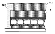
프론트 플레인 적층판의 바람직한 형태는, 전기 광학 매체 및 접착층 없이 전기 도전층이 노출되는 위치에 연결 영역을 가진다. 이 연결 영역이 전기 광학 매체 및 접착층에 의해 둘러싸이도록 전기 광학 매체 및 접착층을 통해 연장하는 개구에 의해서 연결 영역이 형성될 수 있다. 릴리스 시트는 이 연결 영역을 통해 연장하지 않는 것이 바람직하다. 이하에서 더 상세히 설명하는 이유로, 전기 도전성 재료의 접촉 패드는 연결 영역에서 전기 도전층 위에 놓이도록 제공될 수도 있다.A preferred form of the front-plane laminate has a connection area at a position where the electrically conductive layer is exposed without the electro-optical medium and the adhesive layer. The connection region may be formed by an opening extending through the electro-optical medium and the adhesive layer such that the connection region is surrounded by the electro-optic medium and the adhesive layer. The release sheet is preferably not extended through this connection area. For reasons described in more detail below, the contact pads of the electrically conductive material may be provided to lie on the electrically conductive layer in the connection area.
프론트 플레인 적층판은 전기 도전층과 전기 접촉하며, 전기 광학 매체 및 접착층을 통하거나 지나서, 그로부터 연장하는 도전성 비아를 가질 수도 있다. 이러한 형태의 프론트 플레인 적층판에서, 전기 도전층으로부터 멀리 떨어져 있는 도전성 비아의 단부는 릴리스 시트에 의해 피복되지 않는 것이 바람직하다. 도전성 비아는, 중합체 매트릭스에 분산되는 도전성 입자를 포함하는 재료와 같이, 변형가능한 재료로부터 형성될 수도 있다. 전기 도전성 재료의 접촉 패드는 전기 도전층 및 도전성 비아 사이에 개재될 수도 있다.The front-plane laminate may be in electrical contact with the electrically conductive layer, and may have conductive vias extending therethrough or past the electro-optic medium and the adhesive layer. In this type of front-plane laminate, the ends of the conductive vias away from the electrically conductive layer are preferably not covered by the release sheet. The conductive vias may be formed from a deformable material, such as a material comprising conductive particles dispersed in a polymer matrix. The contact pads of the electrically conductive material may be interposed between the electrically conductive layer and the electrically conductive vias.
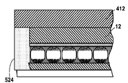
프론트 플레인 적층판의 릴리스 시트에는 제 2 전기 도전층이 제공될 수도 있다. 이 제 2 전기 도전층은 릴리스 시트의 어느 하나의 표면상에 제공될 수도 있지만, 통상적으로는 전기 광학 매체에 더 근접한 표면상에 제공될 것이다. 이하에서 설명하는 바와 같이, 이 제 2 전기 도전층이, 디스플레이로의 합체 전에 프론트 플레인 적층판을 검사하는데 유용하다. 다른 방법으로는 또는 부가하여, 프론트 플레인 적층판은 전기 광학 매체로부터 전기 도전층의 반대측상의 보조 접착층을 가질 수 있으며, 보조 접착층을 피복하는데 보조 릴리스 시트가 제공될 수도 있다.The release sheet of the front-plane laminate may be provided with a second electrically conductive layer. This second electrically conductive layer may be provided on either surface of the release sheet, but will typically be provided on a surface closer to the electro-optic medium. As will be described below, this second electrically conductive layer is useful for inspecting the front-plane laminate before incorporation into a display. Alternatively or additionally, the front-plane laminate may have an auxiliary adhesive layer on the opposite side of the electrically conductive layer from the electro-optic medium, and an auxiliary release sheet may be provided to cover the auxiliary adhesive layer.
다른 양태에서, 본 발명은 광투과 전기 도전층; 전기 도전층과 전기 접촉하는 고체 전기 광학 매체층; 및 접착층을 순서대로 포함하는 제 2 제품 (또는 프론트 플레인 적층판) 을 제공한다. 이 제품은 전기 광학 매체 및 접착층 없이 전기 도전층이 노출되는 연결 영역을 가진다.In another aspect, the present invention provides a light-transmitting electroconductive layer; A solid electro-optic medium layer in electrical contact with the electrically conductive layer; And a second product (or a front-plane laminated plate) including an adhesive layer in this order. The product has a connection area where the electrically conductive layer is exposed without the electro-optic medium and the adhesive layer.
이 프론트 플레인 적층판에서, 연결 영역은 적층판의 에지에서 연장할 수도 있고 연장하지 않을 수도 있지만, 연결 영역이 전기 광학 매체 및 접착층에 의해 둘러싸이도록 연결 영역이 전기 광학 매체 및 접착층을 통해 연장하는 개구에 의해서 형성되도록 하는, 후자가 일반적으로 바람직하다. 프론트 플레인 적층판은 전기 광학 매체층으로부터 그 반대측상에 있는 접착층에 인접하게 배치되는 릴리스 시트를 더 포함할 수 있다. 릴리스 시트는 연결 영역을 통해 연장하지 않을 수도 있다. 릴리스 시트에는 제 2 전기 도전층이 제공될 수 있다. 프론트 플레인 적층판은 연결 영역에서 전기 도전층 위에 놓이는 전기 도전성 재료의 접촉 패드를 더 포함할 수 있으며, 이하에서 설명하는 이유로, 이러한 접촉 패드의 존재는 연결 영역에서의 전기 도전층에서 두께가 증가되는 바람직한 영역을 효과적으로 제공한다. 이 프론트 플레인 적층판은 상술한 타입 중 임의의 고체 전기 광학 매체를 이용할 수 있지만, 전기 광학 매체는 전기영동 매체, 바람직하게는 캡슐화된 전기영동 매체인 것이 일반적으로 바람직하다. In this front-plane laminate, the connection area may or may not extend at the edge of the laminate, but the connection area is formed by an opening extending through the electro-optic medium and the adhesive layer so that the connection area is surrounded by the electro- The latter being generally preferred. The front-plane laminate may further include a release sheet disposed adjacent to the adhesive layer on the opposite side from the electro-optical medium layer. The release sheet may not extend through the connection area. The release sheet may be provided with a second electrically conductive layer. The front-plane laminate may further comprise a contact pad of an electrically conductive material that overlies the electrically conductive layer in the connection area, and for the reasons described below, the presence of such a contact pad is preferred, Area effectively. Although this front plane laminate can use any of the above-mentioned types of solid electro-optical media, it is generally preferable that the electro-optical medium is an electrophoresis medium, preferably an encapsulated electrophoresis medium.
다른 양태에서, 본 발명은 광투과 전기 도전층; 상기 전기 도전층과 전기접촉하는 고체 전기 광학 매체층; 및 접착층을 순서대로 포함하는 제 3 제품 (프론트 플레인 적층판) 을 제공한다. 그러나, 본 발명의 제 3 프론트 플레인 적층판은 상기 전기 도전층과 전기접촉하며 상기 전기 광학 매체 및 상기 접착층을 통하거나 또는 지나서 그로부터 연장하는 도전성 비아를 더 포함한다.In another aspect, the present invention provides a light-transmitting electroconductive layer; A solid electro-optical medium layer in electrical contact with the electrically conductive layer; And a third product (front-plane laminate) including an adhesive layer in this order. However, the third front plane laminate of the present invention further includes a conductive via in electrical contact with the electrically conductive layer and extending therethrough or past the electro-optic medium and the adhesive layer.
본 발명의 제 3 프론트 플레인 적층판은 전기 광학 매체층으로부터 그 반대측상에 있는 접착층에 인접하게 배치되는 릴리스 시트를 더 포함할 수도 있다. 전기 도전층으로부터 멀리 떨어져 있는 도전성 비아의 단부는 릴리스 시트에 의해 피복되지 않을 수도 있다. 도전성 비아는 변형가능한 재료 예를 들면, 중합체 매트릭스에 분산되는 도전성 입자를 포함하는 재료로부터 형성될 수도 있다. 본 발명의 다른 프론트 플레인 적층판과 유사하게, 동일한 이유에서, 제 3 프론트 플레인 적층판은 연결 영역에서 전기 도전층 위로 놓이는 전기 도전성 재료의 접촉 패드를 더 포함할 수도 있다. 제 3 프론트 플레인 적층판은 상술한 타입 중 임의의 고체 전기 광학 매체를 이용할 수 있지만, 전기 광학 매체는 전기영동 매체, 바람직하게는 캡슐화된 전기영동 매체인 것이 일반적으로 바람직하다.The third front plane laminate of the present invention may further comprise a release sheet disposed adjacent to the adhesive layer on the opposite side from the electro-optical medium layer. The ends of the conductive vias away from the electrically conductive layer may not be covered by the release sheet. The conductive vias may be formed from a material comprising a deformable material, for example, conductive particles dispersed in a polymer matrix. Similar to other front-plane laminate boards of the present invention, for the same reason, the third front-plane laminate board may further comprise contact pads of electrically conductive material overlying the electrically conductive layer in the connection area. Although the third front plane laminate can use any of the above-described types of solid electro-optical media, it is generally preferable that the electro-optical medium is an electrophoresis medium, preferably an encapsulated electrophoresis medium.
또한, 본 발명은 광투과 전기 도전층; 상기 전기 도전층과 전기접촉하는 고체 전기 광학 매체층; 접착층; 및 하나 이상의 화소 전극을 가지는 백플레인을 순서대로 포함하고, 상기 전기 도전층과 상기 화소 전극 사이의 전위의 인가에 의해 상기 전기 광학 매체의 광학적 상태가 변화될 수 있도록 하며, 상기 백플레인은 하나 이상의 화소 전극으로부터 전기 절연되는 하나 이상의 접촉 패드를 더 포함하는 전기 광학 디스플레이를 제공한다. 이 디스플레이는, 전기 도전층으로부터 전기 광학 매체 및 접착층을 통하거나 지나서 상기 접촉 패드로 또는 상기 접촉 패드 중 하나까지 연장하는 하나 이상의 도전성 비아를 더 포함한다.The present invention also provides a light-transmitting electroconductive layer; A solid electro-optical medium layer in electrical contact with the electrically conductive layer; Adhesive layer; And a backplane having one or more pixel electrodes in order, wherein an optical state of the electro-optic medium can be changed by application of a potential between the electroconductive layer and the pixel electrode, And at least one contact pad electrically isolated from the at least one contact pad. The display further comprises one or more conductive vias extending from the electrically conductive layer to the electro-optic medium and the adhesive layer or to the contact pad or to one of the contact pads.
전술한 바와 같이, 이 디스플레이에서, 도전성 비아는 전기 광학 매체를 통하거나 지나서 연장할 수도 있지만, 도전성 비아가 전기 광학 매체 및 접착층을 통해 연장함으로써, 도전성 비아가 전기 광학 매체 및 접착층에 의해 완전히 둘러싸이도록 하는 전자의 배열이 일반적으로 바람직하다. 도전성 비아는 변형가능한 재료, 예를 들면 중합체 매트릭스에서 분산되는 도전성 입자를 포함하는 재료로부터 형성될 수도 있다. 디스플레이는 전술한 타입 중 임의의 고체 전기 광학 매체를 이용할 수도 있지만, 전기 광학 매체는 전기영동 매체, 바람직하게는 캡슐화된 전기영동 매체인 것이 일반적으로 더 바람직하다.As discussed above, in this display, the conductive vias may extend through or past the electro-optic medium, but the conductive vias extend through the electro-optic medium and the adhesive layer such that the conductive vias are completely surrounded by the electro- Is generally preferred. The conductive vias may be formed from a material that includes a deformable material, for example, conductive particles that are dispersed in a polymer matrix. It is generally preferred that the electro-optic medium is an electrophoretic medium, preferably an encapsulated electrophoretic medium, although the display may utilize any of the foregoing types of solid electro-optic media.
본 발명의 전기 광학 디스플레이에는 전기 광학 매체로부터 전기 도전층의 반대측상에 배치되는 보호 및/또는 배리어층이 제공될 수도 있다. 투명 접착층이 전기 도전층에 대해 보호 및/또는 배리어층을 확보하는데 이용될 수도 있다. 전기 광학 디스플레이는 전기 광학 매체층의 주변의 적어도 일부 주위에 배치되는 밀봉 재료를 가질 수도 있다. 이러한 밀봉된 디스플레이의 일 형태에서, 보호 및/또는 배리어층은 전기 광학 매체의 주변을 넘어 연장하여 제공되며, 보호 및/또는 배리어층과 백플레인 사이의 전기 광학 매체의 주변 중 적어도 일부 주위에 밀봉재료가 배치된다.The electro-optic display of the present invention may be provided with a protective and / or barrier layer disposed on the opposite side of the electro-conductive layer from the electro-optic medium. A transparent adhesive layer may also be used to protect and / or secure the barrier layer against the electrically conductive layer. The electro-optic display may have a sealing material disposed around at least a portion of the periphery of the electro-optic medium layer. In one form of such a sealed display, the protective and / or barrier layer is provided extending beyond the periphery of the electro-optic medium and is provided around at least a portion of the periphery of the protective and / or barrier layer and the back- .
다른 양태에서, 본 발명은 고체 전기 광학 디스플레이를 제조하기 위한 방법을 제공한다. 이 방법은 광투과 전기 도전층; 상기 전기 도전층과 전기접촉하는 고체 전기 광학 매체층; 접착층; 및 릴리스 시트를 순서대로 포함하는 제품을 제공하는 단계를 포함한다. 이 방법은 복수의 화소 전극을 포함하는 백플레인 및 상기 화소 전극들에 가변 전위를 인가하도록 배열되는 구동 수단을 제공하는 단계를 더 포함한다. 또한, 이 방법은 상기 접착층으로부터 릴리스 시트를 제거하는 단계 및 상기 접착층을 상기 백플레인에 부착하도록 하는 조건들의 효과하에서 상기 접착층을 상기 백플레인과 접착시킴으로써, 상기 백플레인으로 접착층, 전기 광학 매체층 및 전기 도전층을 확보하는 단계를 포함한다.In another aspect, the present invention provides a method for manufacturing a solid electro-optic display. The method comprises: providing an optically transparent electrically conductive layer; A solid electro-optical medium layer in electrical contact with the electrically conductive layer; Adhesive layer; And a release sheet in order. The method further includes providing a backplane including a plurality of pixel electrodes and a driving means arranged to apply a variable potential to the pixel electrodes. The method also includes bonding the adhesive layer to the backplane under the effect of conditions to remove the release sheet from the adhesive layer and to adhere the adhesive layer to the backplane so that the adhesive layer, .
이 방법에서, 백플레인과 접착층의 접촉은 대략 20 내지 대략 60 퍼센트의 상대 습도하에서 달성되는 것이 바람직하다. 이하에서 더 상세하게 설명하는 바와 같이, 정전기 방전으로 인한 문제를 방지하기 위해서, 본 방법은 접착층으로부터 하나 이상의 릴리스 시트의 제거 및 접착층을 백플레인과 접촉시키는 동안에, 프론트 플레인 적층판으로 이온화된 입자들을 인가하는 단계를 포함할 수도 있다.In this manner, contact between the backplane and the adhesive layer is preferably achieved at a relative humidity of from about 20 to about 60 percent. As will be described in greater detail below, in order to avoid problems due to electrostatic discharge, the method includes removing one or more release sheets from the adhesive layer and applying ionized particles to the front-plane laminate during contact of the adhesive layer with the backplane Step < / RTI >
이 방법에서, 프론트 플레인 적층판에는 전기 광학 매체 및 접착층 없이 전기 도전층이 노출되는 위치의 연결 영역이 제공되며, 백플레인에는 화소 전극으로부터 전기 절연되는 접촉 패드가 제공될 수도 있으며, 이 방법은 연결 영역을 접촉 패드와 전기접촉하여 위치시킬 수 있다. 연결 영역은 전기 광학 매체 및 접착층을 통해 연장하는 개구에 의해 형성되며, 백플레인과 접착층을 접촉시키기 이전에 접촉 패드상에 변형가능한 전기 도전성 재료가 배치될 수 있어서, 백플레인과 접착층을 접촉시키는 동안에는, 변형가능한 전기 도전성 재료가 개구로 들어가서 접촉 패드를 전기 도전층에 전기 접속시키는 도전성 비아를 형성하도록 한다. 다른 방법으로는, 전기 광학 매체 및 접착층을 통해 전기 도전층으로부터 연장하는 도전성 비아가 연결 영역에 제공될 수 있으며, 이 방법은 접촉 패드와 전기 접촉하도록 도전성 비아를 배치한다.In this method, the front-plane laminated plate is provided with a connecting area at a position where the electro-conductive medium and the adhesive layer are exposed, and the backplane is provided with a contact pad electrically insulated from the pixel electrode, It can be placed in electrical contact with the contact pad. The connecting area is defined by the electro-optic medium and an opening extending through the adhesive layer, and a deformable electrically conductive material may be disposed on the contact pad prior to contacting the backplane with the adhesive layer such that during contact with the backplane, A possible electrically conductive material enters the opening to form a conductive via that electrically connects the contact pad to the electrically conductive layer. Alternatively, a conductive via extending from the electrically conductive layer through the electro-optic medium and the adhesive layer may be provided in the connection region, the method placing conductive vias in electrical contact with the contact pads.
본 방법은 전기 광학 매체로부터 전기 도전층의 반대측상에 보호 및/또는 배리어층을 제공하는 단계를 포함할 수도 있다. 이러한 목적에서, 프론트 플레인 적층판은 전기 광학 매체로부터 전기 도전층의 반대측상의 보조 접착층을 포함할 수도 있으며, 본 방법은 보호 및/또는 배리어층을 보조 접착층에 부착시킬 수 있다. 프론트 플레인 적층판은 보조 접착층을 피복하는 보조 릴리스 시트를 가질 수도 있으며, 본 방법은 보조 접착층이 보호 및/또는 배리어층에 부착되기 전에, 보조 접착층으로부터 보조 릴리스 시트를 제거하는 단계를 포함한다.The method may include providing a protective and / or barrier layer on the opposite side of the electrically conductive layer from the electro-optic medium. For this purpose, the front-plane laminate may comprise an auxiliary adhesive layer on the opposite side of the electrically conductive layer from the electro-optic medium, and the method may adhere the protective and / or barrier layer to the auxiliary adhesive layer. The front-plane laminate may have an auxiliary release sheet covering the auxiliary adhesive layer, and the method includes removing the auxiliary release sheet from the auxiliary adhesive layer before the auxiliary adhesive layer is adhered to the protective and / or barrier layer.
이 방법에서, 릴리스 시트에는 제 2 전기 도전층이 제공될 수도 있으며, 이 방법은 광투과 전기 도전층과 제 2 전기 도전층 사이에 전기 광학 매체의 광학적 상태를 변화시키기에 충분한 전압을 인가하는 단계를 포함한다.In this method, the release sheet may be provided with a second electrically conductive layer, which method comprises applying a voltage between the optically transparent electroconductive layer and the second electrically conductive layer sufficient to change the optical state of the electro- .
이 방법은 회전 바이크로멀 부재 매체 또는 전자크로믹 매체와 같은 전술한 타입 중 임의의 전기 광학 매체를 이용할 수도 있지만, 전기 광학 매체는 전기영동 매체인 것이 바람직하고, 캡슐화된 전기영동 매체인 것이 더 바람직하다.Although the method may use any of the above-described types of electro-optic mediums such as a marble medium or an electrochromic medium as a rotating bike, the electro-optical medium is preferably an electrophoretic medium, and more preferably an encapsulated electrophoretic medium desirable.
다른 양태에서, 본 발명은 전기 광학 디스플레이를 형성하는 방법을 제공한다. 본 방법은, In another aspect, the invention provides a method of forming an electro-optic display. In this method,
광투과 전기 도전층; 그 전기 도전층과 전기접촉하는 고체 전기 광학 매체층; 및 접착층을 순서대로 포함하는 프론트 조립품을 제공하는 단계;A light transmission electrically conductive layer; A solid electro-optic medium layer in electrical contact with the electrically conductive layer; And an adhesive layer in this order;
상기 프론트 조립품의 일부로부터 상기 전기 광학 매체 및 상기 접착층을 제거함으로써, 상기 전기 광학 매체 및 상기 접착층 없이 전기 도전층이 노출되는 연결 영역을 제공하는 단계;Providing a connection region in which the electro-optic medium and the adhesive layer are removed from a portion of the front assembly, thereby exposing the electro-optic medium and the electrically conductive layer without the adhesive layer;
상기 연결 영역상에 도전성 비아를 형성하는 단계;Forming a conductive via on the connection region;
하나 이상의 화소 전극 및 상기 하나 이상의 화소 전극으로부터 전기 절연되는 하나 이상의 접촉 패드를 포함하는 백플레인을 제공하는 단계; 및Providing a backplane comprising at least one pixel electrode and at least one contact pad electrically isolated from the at least one pixel electrode; And
상기 전기 광학 매체가 상기 하나 이상의 화소 전극에 인접하게 배치되고 상기 도전성 비아는 상기 하나 이상의 접촉 패드와 전기접촉하는 상태로, 상기 전기 도전층이 상기 도전성 비아를 통하여 하나 이상의 접촉 패드에 전기접속되도록 하여, 상기 접착층이 상기 백플레인에 부착되도록, 상기 백플레인에 상기 프론트 조립품을 적층하는 단계를 포함한다.The electrically conductive layer is electrically connected to one or more contact pads through the conductive via in a state where the electro-optic medium is disposed adjacent to the one or more pixel electrodes and the conductive via is in electrical contact with the one or more contact pads And laminating the front assembly to the backplane so that the adhesive layer is attached to the backplane.
본 방법에서, 연결 영역은, 전기 광학 매체 및 접착층에 의해 연결 영역이 둘러싸이도록 전기 광학 매체 및 접착층을 통해 연장하는 개구에 의해 형성될 수도 있다. 프론트 조립품은 전기 광학 매체층으로부터 그 반대측상에 있는 접착층에 인접하게 배치되는 릴리스 시트를 포함하며, 이 릴리스 시트는 프론트 조립품이 백플레인에 적층되기 전에 접착층으로부터 제거될 수도 있다. 이러한 릴리스 시트가 존재하는 경우, 프론트 조립품의 일부로부터 전기 광학 매체 및 접착층을 제거하는 단계는, 연결 영역이 릴리스 시트가 없도록 프론트 조립품의 일부로부터 릴리스 시트를 제거하는 단계를 또한 포함할 수도 있다. 릴리스 시트에 제 2 전기 도전층이 제공될 수 있으며, 이 방법은 광투과 전기 도전층과 제 2 전기 도전층 사이에 전기 광학 매체의 광학적 상태를 변화시키기에 충분한 전압을 인가하는 단계를 포함할 수 있다.In the present method, the connection region may be formed by an opening extending through the electro-optical medium and the adhesive layer such that the connection region is surrounded by the electro-optical medium and the adhesive layer. The front assembly includes a release sheet disposed adjacent the adhesive layer on the opposite side of the electro-optic medium layer, which release sheet may be removed from the adhesive layer before the front assembly is laminated to the backplane. When such a release sheet is present, removing the electro-optic medium and the adhesive layer from a portion of the front assembly may also include removing the release sheet from a portion of the front assembly such that the connection area does not have a release sheet. The release sheet may be provided with a second electrically conductive layer which may comprise applying a voltage between the optically transparent electrically conductive layer and the second electrically conductive layer sufficient to change the optical state of the electro- have.
본 발명의 이 방법에서, 도전성 비아는 변형가능한 재료, 예를 들면 중합체 매트릭스에서 도전성 입자들을 포함하는 재료로부터 형성될 수도 있다.In this method of the invention, the conductive vias may be formed from a deformable material, for example, from a material comprising conductive particles in a polymer matrix.
본 발명의 이 방법에서, 도전성 비아는 적층 단계 이전에 프론트 조립품에 존재할 수도 있으며 또는 적층 단계 동안에 형성될 수도 있다. 후자의 경우에, 프론트 조립품을 백플레인으로 적층하는 동안에 도전성 비아의 형성이 일어나도록, 도전성 비아를 형성할 재료가 적층 단계 이전에 백플레인상에 위치될 수 있다. 위에서 간단히 설명하고 이하에 상세히 설명할 이유로, 프론트 조립품은 전기 도전층의 일부 위에 놓이는 전기 도전성 재료의 프론트 접촉 패드를 가질 수도 있으며, 연결 영역은 프론트 접촉 패드의 적어도 일부를 노출하도록 형성될 수도 있다.In this method of the present invention, the conductive vias may be present in the front assembly prior to the laminating step, or may be formed during the laminating step. In the latter case, the material to form the conductive vias may be placed on the backplane prior to the laminating step so that the formation of conductive vias occurs during lamination of the front assembly to the backplane. For the purposes of the foregoing briefly and described below in detail, the front assembly may have a front contact pad of electrically conductive material overlying a portion of the electrically conductive layer, and the connection area may be formed to expose at least a portion of the front contact pad.
본 발명의 이 방법에서, 프론트 조립품은 전기 광학 매체로부터 전기 도전층의 반대측 상에 투명 접착층 및 투명 접착층에 인접하게 배치되는 제 2 릴리스 시트를 가질 수 있으며, 이 방법은 투명 접착층으로부터 제 2 릴리스 시트를 제거하는 단계 및 보호 및/또는 배리어층에 투명 접착층을 적층하는 단계를 포함할 수도 있다. 통상적으로, 제 2 릴리스 시트의 제거 및 투명 접착층의 적층은 프론트 조립품을 백플레인에 적층한 후에 달성될 것이다.In this method of the present invention, the front assembly may have a transparent release layer on the opposite side of the electrically conductive layer from the electro-optic medium and a second release sheet disposed adjacent the transparent release layer, And laminating a transparent adhesion layer on the protective and / or barrier layer. Typically, the removal of the second release sheet and the lamination of the transparent adhesive layer will be accomplished after the front assembly is laminated to the backplane.
본 발명의 이 방법에서, 프론트 조립품을 백플레인에 적층한 후에, 프론트 조립품의 주변의 적어도 일부의 주위에 밀봉재료가 위치될 수도 있다. 전술한 바와 같이, 디스플레이에 보호 및/또는 배리어층이 제공되는 경우, 이 보호 및/또는 배리어층은 전기 광학 매체의 주변을 넘어서 연장할 수도 있으며, 보호 및/또는 배리어층과 백플레인 사이의 전기 광학 매체 주변의 적어도 일부의 주위에 밀봉재료가 위치될 수도 있다.In this method of the present invention, after the front assembly is laminated to the backplane, the sealing material may be positioned around at least a portion of the periphery of the front assembly. As discussed above, when a protective and / or barrier layer is provided on the display, the protective and / or barrier layer may extend beyond the perimeter of the electro-optic medium and may include protective and / or electro- The sealing material may be located around at least a portion of the periphery of the media.
또한, 본 발명은 전기 광학 디스플레이를 형성하는 다른 방법을 제공한다. 이 다른 방법은, The present invention also provides another method of forming an electro-optic display. In this alternative method,
광투과 전기 도전층을 포함하는 기판을 제공하는 단계;Providing a substrate comprising a light transmissive electrically conductive layer;
상기 기판의 일부 위에 고체 전기 광학 매체를 코팅하여 상기 기판의 연결 영역을 코팅되지 않은 상태로 남겨두는 단계;Coating a portion of the substrate with a solid electro-optic medium to leave the connection region of the substrate in an uncoated state;
상기 전기 광학 매체 위에 접착층을 코팅하여, 상기 연결 영역을 코팅되지 않은 상태로 남겨둠으로써, 프론트 조립품을 형성하는 단계;Forming a front assembly by coating an adhesive layer on the electro-optic medium to leave the connection area uncoated;
하나 이상의 화소 전극 및 상기 하나 이상의 화소 전극으로부터 전기 절연되는 접촉 패드를 포함하는 백플레인을 제공하는 단계; 및Providing a backplane including at least one pixel electrode and a contact pad electrically insulated from the at least one pixel electrode; And
전기 광학 매체가 하나 이상의 화소 전극에 인접하게 배치되고 상기 연결 영역에서 상기 전기 도전층이 접촉 패드와 전기접촉하는 상태로, 상기 접착층이 상기 백플레인에 부착하도록, 상기 백플레인에 상기 프론트 조립품을 적층하는 단계를 포함한다.Laminating the front assembly to the backplane so that the adhesive layer adheres to the backplane with the electro-optic medium disposed adjacent to the at least one pixel electrode and the electrically conductive layer in electrical contact with the contact pad in the connection region .
본 발명의 이 방법은, 접착층 위에 릴리스 시트를 위치시키는 단계를 포함할 수도 있으며, 이 릴리스 시트는 프론트 조립품을 백플레인에 적층하기 전에 접착층으로부터 제거될 것이다. 릴리스 시트에는 제 2 전기 도전층이 제공될 수도 있으며, 이 방법은 광투과 전기 도전층과 제 2 전기 도전층 사이에 전기 광학 매체의 광학적 상태를 변화시키는데 충분한 전압을 인가하는 단계를 포함할 수 있다. 이 방법은, 연결 영역에 있는 전기 도전층이 변형가능한 전기 도전성 재료를 통해 접촉 패드에 접속되도록, 프론트 조립품을 백플레인에 적층하기 전에 백플레인의 접촉 패드상에 변형가능한 전기 도전성 재료를 위치시키는 단계를 포함할 수도 있다.The method of the present invention may also include positioning the release sheet over the adhesive layer, which release sheet will be removed from the adhesive layer prior to laminating the front assembly to the backplane. The release sheet may also be provided with a second electrically conductive layer, which may comprise applying a voltage between the optically transparent electrically conductive layer and the second electrically conductive layer, sufficient to change the optical state of the electro-optic medium . The method includes positioning the deformable electrically conductive material on the contact pads of the backplane prior to laminating the front assembly to the backplane such that the electrically conductive layer in the connection area is connected to the contact pad via a deformable electrically conductive material You may.
본 발명의 이 방법에서, 프론트 조립품은 전기 광학 매체로부터 전기 도전층의 반대측 상의 투명 접착층 및 투명 접착층에 인접하게 배치되는 릴리스 시트를 가질 수도 있으며, 본 방법은, 투명 접착층으로부터 릴리스 시트를 제거하는 단계 및 투명 접착층을 보호 및/또는 배리어층에 적층하는 단계를 포함할 수도 있다. 통상적으로, 릴리스 시트의 제거 및 투명 접착층의 적층은 프론트 조립품을 백플레인에 적층한 후에 달성될 것이다.In this method of the invention, the front assembly may have a release sheet disposed adjacent to the transparent adhesive layer and the transparent adhesive layer on the opposite side of the electrically conductive layer from the electro-optic medium, the method comprising removing the release sheet from the transparent adhesive layer And laminating the transparent adhesion layer on the barrier layer and / or the protection layer. Typically, removal of the release sheet and lamination of the transparent adhesive layer will be accomplished after the front assembly is laminated to the backplane.
본 발명의 이 방법에서, 프론트 조립품을 백플레인에 적층한 후에, 프론트 조립품의 주변의 적어도 일부의 주위에 밀봉재료가 위치될 수도 있다. 전술한 바와 같이, 디스플레이에 보호 및/또는 배리어층이 제공되는 경우, 이 보호 및/또는 배리어층은 전기 광학 매체의 주변을 넘어서 연장할 수도 있으며, 보호 및/또는 배리어층과 백플레인 사이의 전기 광학 매체 주변의 적어도 일부 주위에 밀봉재료가 위치될 수도 있다.In this method of the present invention, after the front assembly is laminated to the backplane, the sealing material may be positioned around at least a portion of the periphery of the front assembly. As discussed above, when a protective and / or barrier layer is provided on the display, the protective and / or barrier layer may extend beyond the perimeter of the electro-optic medium and may include protective and / or electro- The sealing material may be located around at least a portion of the periphery of the media.
다른 양태에서, 본 발명은, 하나 이상의 화소 전극을 포함하는 백플레인; 상기 화소 전극에 인접하게 배치되는 고체 전기 광학 매체층; 상기 백플레인으로부터 전기 광학 매체의 반대측상에 배치되는 광투과 전극; 상기 전기 광학 매체로부터 상기 광투과 전극의 반대측상에 배치되는 보호 및/또는 배리어층; 및 주위환경으로부터 상기 전기 광학 매체내부로의 물질의 진입을 방지하기 위한 밀봉재료로서, 상기 전기 광학 매체층의 주변의 적어도 일부를 따라 배치되며 보호 및/또는 배리어층의 상기 백플레인으로부터 연장하는 상기 밀봉재료를 포함하는, (밀봉된) 전기 광학 디스플레이를 제공한다.In another aspect, the invention provides a backplane comprising: at least one pixel electrode; A solid electro-optical medium layer disposed adjacent to the pixel electrode; A light transmitting electrode disposed on the opposite side of the electro-optical medium from the backplane; A protective and / or barrier layer disposed on the opposite side of the light-transmitting electrode from the electro-optical medium; And a sealing material for preventing entry of a substance from the surrounding environment into the electro-optic medium, the sealing material being disposed along at least a portion of the periphery of the electro-optic medium layer and extending from the backplane of the protective and / (Sealed) electro-optic display comprising a material.
이러한 밀봉된 전기 광학 디스플레이에서, 밀봉재료는 백플레인의 평면에 대해 평행하게 측정되는 측면의 두께를 가질 있으며, 이 두께는 백플레인으로부터 보호 및/또는 배리어층으로 감소한다. 다른 방법으로는, 보호 및/또는 배리어층은 백플레인의 평면에 대해 평행하게 측정되는 전기 광학 매체층보다 더 작을 수도 있으며, 밀봉재료는 전기 광학 매체층의 주변부 위로 연장하며 보호 및/또는 배리어층의 주변과 접촉할 수도 있다. 본 발명의 밀봉된 전기 광학 디스플레이의 다른 변형에서, 보호 및/또는 배리어층은 백플레인의 평면에 대해 평행하게 측정되는 전기 광학 매체층보다 더 클 수도 있으며, 전기 광학 매체층의 주변을 넘어 연장하는 보호 및/또는 배리어층의 주변부와 백플레인 사이에서 밀봉재료가 연장한다.In such a sealed electro-optic display, the sealing material has a lateral thickness which is measured parallel to the plane of the backplane, which thickness is reduced from the backplane to the protective and / or barrier layer. Alternatively, the protective and / or barrier layer may be smaller than the electro-optic medium layer measured parallel to the plane of the backplane, the sealing material extending over the periphery of the electro-optic medium layer and / It may be in contact with the periphery. In another variation of the encapsulated electro-optic display of the present invention, the protective and / or barrier layer may be larger than the electro-optic medium layer measured parallel to the plane of the backplane, And / or the sealing material extends between the periphery of the barrier layer and the backplane.
또한, 본 발명은 하나 이상의 화소 전극을 포함하는 백플레인; 상기 화소 전극에 인접하게 배치되는 고체 전기 광학 매체층; 상기 백플레인으로부터 상기 전기 광학 매체의 반대측상에 배치되는 광투과 전극; 상기 전기 광학 매체로부터 상기 광투과 전극의 반대측상에 배치되는 전극 지지대; 및 주위환경으로부터 상기 전기 광학 매체 내부로의 물질의 진입을 방지하기 위한 밀봉재료로서, 상기 전기 광학 매체층의 주변을 넘어 연장하는 상기 광투과 전극의 주변부와 상기 백플레인 사이에서 연장하는 밀봉재료를 포함하며, 상기 광투과 전극 및 상기 전극 지지대는 상기 백플레인의 평면에 대해 평행하게 측정되는 상기 전기 광학 매체층보다 더 큰, 제 2 (밀봉된) 전기 광학 디스플레이를 제공한다.The present invention also provides a backplane comprising at least one pixel electrode; A solid electro-optical medium layer disposed adjacent to the pixel electrode; A light transmitting electrode disposed on the opposite side of the electro-optical medium from the backplane; An electrode support disposed on the opposite side of the light-transmitting electrode from the electro-optical medium; And a sealing material for preventing entry of a substance from the surrounding environment into the inside of the electro-optical medium, the sealing material comprising a sealing material extending between a periphery of the light-transmitting electrode extending beyond the periphery of the electro- Optical display, wherein the light-transmitting electrode and the electrode support are larger than the electro-optic medium layer measured parallel to the plane of the backplane.
마지막으로, 본 발명은 고체 전기 광학 매체를 검사하는 2 가지 방법을 제공한다. 제 1 방법은, Finally, the present invention provides two methods for inspecting a solid electro-optic medium. In the first method,
광투과 전기 도전층;A light transmission electrically conductive layer;
상기 전기 도전층과 전기접촉하는 고체 전기 광학 매체층;A solid electro-optical medium layer in electrical contact with the electrically conductive layer;
접착층; 및Adhesive layer; And
제 2 전기 도전층을 가지는 릴리스 시트를 순서대로 포함하여 제조하는 제품을 제공하는 단계;Providing a release sheet having a second electrically conductive layer in order;
상기 2 개의 전기 도전층 사이에 전위차를 인가하여 상기 매체상에 이미지를 형성하는 단계; 및Applying an electrical potential difference between the two electrically conductive layers to form an image on the medium; And
이렇게 형성된 이미지를 관측하는 단계를 포함한다.And observing the thus formed image.
본 발명의 제 2 검사 방법은,In the second inspection method of the present invention,
광투과 전기 도전층;A light transmission electrically conductive layer;
상기 전기 도전층과 전기접촉하는 고체 전기 광학 매체층;
A solid electro-optical medium layer in electrical contact with the electrically conductive layer;
*접착층; 및* Adhesive layer; And
릴리스 시트를 순서대로 포함하는 제품을 제공하는 단계;Providing a product comprising a release sheet in order;
상기 릴리스 시트상에 정전하를 배치하여, 상기 매체상에 이미지를 형성하는 단계; 및Disposing an electrostatic charge on the release sheet to form an image on the medium; And
이렇게 형성된 이미지를 관측하는 단계를 포함한다.And observing the thus formed image.
본 발명의 프론트 플레인 적층판의 하나의 중요한 이점은, 최종 디스플레이로의 합체 이전에 적층판의 품질을 검사할 수 있다는 점이다. 보이드, 줄무늬, 코팅된 층의 두께의 변화, 포인트 박리와 같은 도전성 재료의 디스플레이 흠결 및 코팅된 재료의 성능에 부작용을 일으키거나 비정상적인 것으로 만들 수 있는 다른 문제들이, 코팅 기술 분야의 당업자에게 잘 알려져 있다. 또한, 캡슐화된 전기 광학 매체는 코팅 동안의 캡슐의 파열로 인한 결함으로부터 손해가 발생된다. 따라서, 일반적으로, 최종 제품에 이용하기 전에 임의의 결함을 확인하기 위해서, 눈으로나 기계 비젼 시스템으로 코팅된 제품을 조사하는 것이 필요하다. 실제로 이러한 디스플레이의 능동 매트릭스형 백플레인의 비용은 전기 광학 매체 및 프론트 전극 구조를 합한 비용보다 훨씬 많기 때문에, 능동 매트릭스형 디스플레이에 이용될 전기 광학 매체에는 특히 이런 조사가 필수적이며, 결함이 있는 코팅의 전기 광학 매체가 백플레인에 적층되는 경우, 일반적으로 백플레인을 보존하면서 매체를 제거하는 방법은 없기 때문에, 매체 및 백플레인 양자를 폐기해야만 한다.One important advantage of the front-plane laminate of the present invention is that the quality of the laminate can be checked prior to incorporation into the final display. Other problems that can cause side effects or make abnormalities in the performance of coated materials such as voids, stripes, changes in the thickness of the coated layer, defective display of conductive materials such as point peeling, and other problems are well known to those skilled in the coating arts . In addition, encapsulated electro-optic media suffer damage from defects due to rupture of the capsules during coating. Thus, in general, it is necessary to inspect the coated product with an eye or a machine vision system to identify any defects prior to use in the finished product. Indeed, such an investigation is essential for the electro-optic medium to be used in active matrix type displays, since the cost of the active matrix backplane of such a display is much greater than the combined cost of the electro-optic medium and the front electrode structure, When an optical medium is stacked on a backplane, since there is generally no way to remove the medium while preserving the backplane, both the medium and the backplane must be discarded.
불행히도, 전기 광학 매체의 조사는 다른 코팅된 재료와 비교할 때 고유의 어려움을 나타낸다. 전기장에 노출될 때 전기 광학 매체만이 광학적 상태에서 중대한 변화를 겪게 되며, 광학적 상태에 변화를 겪은 매체의 성능에 부작용을 일으키는 여러 타입의 코팅 흠결 (예를 들면, 접착층내의 함유물 또는 불순물, 또는 캡슐의 파열) 을 시각적으로 관측하기는 매우 어렵다. 따라서, 검사 동안에 매체에 전기장을 인가할 수 있는 것이 바람직하다. 그러나, 대부분의 종래 기술의 공정에서는 이것이 불가능하다. 통상적으로, 이러한 종래의 기술 공정에서, 백플레인 및 프론트 전극 구조는 별개로 형성되며, 전기 광학 매체층은 이들 컴포넌트 중 하나 (일반적으로 프론트 전극 구조) 상에 제공되며, 백플레인 및 프론트 전극 구조는 이들 사이에 끼워진 전기 광학 매체와 함께 적층된다. 이러한 공정은 전기 광학 매체가 이 광학적 상태 사이에 스위칭될 수 있는 적층 이전의 어느 시점을 제공하지 않으며, 따라서 전기 광학 매체 또는 접착제의 흠결은 최종 디스플레이의 형성 이후까지는 발견되지 않을 수도 있으며, 그 결과 흠결이 있는 전기 광학 매체 또는 접착제에 적층되게 되는 양호한 백플레인을 폐기하는 손해가 발생된다. (대부분의 경우에, 매체 또는 전극상의 표면 불규칙은 매체의 광학적 상태에서 균일한 변화를 생성시키는 것을 불가능하게 만들고, 광학적 상태의 이러한 균일한 변화는 매체의 완전한 검사를 요구하기 때문에, 단순히 전극에 대해 기계적으로 프레스하는 것으로 전기 광학 매체를 적절히 검사하는 것은 불가능하다는 점을 유의한다). Unfortunately, irradiation of electro-optic media presents inherent difficulties when compared to other coated materials. When exposed to an electric field, only the electro-optic medium undergoes significant changes in the optical state, and various types of coating defects (e.g., inclusions or impurities in the adhesive layer, or the like) that cause adverse effects on the performance of the medium undergoing a change in optical state Rupture of the capsule) is very difficult to visually observe. It is therefore desirable to be able to apply an electric field to the medium during the inspection. However, this is not possible with most prior art processes. Typically, in this prior art process, the backplane and the front electrode structure are formed separately, and the electro-optic medium layer is provided on one of these components (typically the front electrode structure) And is stacked together with the electro-optical medium sandwiched between the electrodes. This process does not provide any point in time before lamination where the electro-optic medium can be switched between these optical states, and thus defects in the electro-optic medium or glue may not be found until after the formation of the final display, There is a risk of discarding a good backplane to be laminated on the electro-optical medium or adhesive. (In most cases, surface irregularities on the medium or electrode make it impossible to produce a uniform change in the optical state of the medium, and since this uniform variation of the optical state requires complete inspection of the medium, Note that it is impossible to adequately inspect the electro-optic medium by mechanically pressing it).
도 1은 디스플레이에 적층판을 통합하기 이전에, 릴리스 시트가 적층판으로부터 벗겨지는 방식을 나타내는 본 발명의 프론트 플레인 적층판의 개략 단면도이다.
도 2는 검사중인 본 발명의 제 2 프론트 플레인 적층판의, 도 1 과 유사한, 개략 단면도이다.
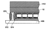
도 3은 검사중인 도 1의 프론트 플레인 적층판을 도시하는, 도 1 과 유사한, 개략 단면도이다.
도 4는 도 3에 도시된 검사 방법을 실행하는 장치의 개략 측면도이다.
도 5, 도 6, 및 도 7은 도 4에 개략적으로 도시되는 장치의 3 개의 실제적인 형태를 도시한다.
도 8은 본 발명의 제 3 프론트 플레인 적층판의, 도 1 과 유사한 개략 단면도이다.
도 9는 본 발명의 제 4 프론트 플레인 적층판의, 도 8 과 유사한, 개략 단면도이다.
도 10은 본 발명의 제 1 전기 광학 디스플레이를 형성하기 위하여 공정의 중간 단계에서 이용되는 도 9의 프론트 플레인 적층판을 도시하는 개략 단면도이다.
도 11은 본 발명의 제 1 전기 광학 디스플레이의 최종 형태를 도시하는 개략 단면도이다.
도 12 내지 도 17은 상이한 밀봉 구성을 이용하여 전기 광학 디스플레이의 변형된 형태를 도시하는, 도 11 과 유사한, 개략 단면도이다.
도 18은 검사가 진행중인 본 발명의 제 5 프론트 플레인 적층판의 개략 단면도이다.
도 19는 본 발명의 공정에서 도 18의 프론트 플레인 적층판이 백플레인에 적층되는 것을 도시하는 개략 단면도이다.
도 20은 중간 단계가 도 19에 도시되는 공정에 의해 제조되는 최종 전기 광학 디스플레이의 개략 단면도이다.
*도 21 및 22는 본 발명의 프론트 플레인 적층판을 형성하는 코팅 공정의 개략 평면도이다.BRIEF DESCRIPTION OF THE DRAWINGS Figure 1 is a schematic cross-sectional view of a front-plane laminate of the present invention showing the manner in which release sheets are peeled from the laminate before incorporating the laminate into the display.
Figure 2 is a schematic cross-sectional view similar to Figure 1 of a second front-plane laminate of the present invention under inspection.
Fig. 3 is a schematic cross-sectional view similar to Fig. 1, showing the front-plane laminate of Fig. 1 being inspected.
Figure 4 is a schematic side view of an apparatus for carrying out the inspection method shown in Figure 3;
Figures 5, 6 and 7 illustrate three practical forms of the device shown schematically in Figure 4.
Fig. 8 is a schematic cross-sectional view similar to Fig. 1 of the third front-plane laminate of the present invention.
Fig. 9 is a schematic cross-sectional view similar to Fig. 8 of the fourth front-plane laminate of the present invention.
Figure 10 is a schematic cross-sectional view showing the front-plane laminate of Figure 9 used in the middle step of the process to form the first electro-optic display of the present invention.
11 is a schematic cross-sectional view showing the final form of the first electro-optical display of the present invention.
Figs. 12-17 are schematic cross-sectional views similar to Fig. 11, showing a modified form of an electro-optic display using different sealing configurations.
18 is a schematic cross-sectional view of a fifth front plane laminate of the present invention under examination.
Fig. 19 is a schematic sectional view showing that the front-plane laminated sheet of Fig. 18 is laminated on the backplane in the process of the present invention. Fig.
20 is a schematic cross-sectional view of a final electro-optic display in which the intermediate step is manufactured by the process shown in Fig.
21 and 22 are schematic plan views of a coating process for forming the front-plane laminate of the present invention.
본 발명의 바람직한 실시형태는, 첨부 도면을 참조하여 예시만의 방법으로 설명한다.Preferred embodiments of the present invention will be described by way of example only with reference to the accompanying drawings.
전술한 바와 같이, 본 발명은 광투과 전기 도전층; 상기 광투과 전기 도전층과 전기접촉하는 고체 전기 광학 매체층; 접착층; 및 릴리스 시트를 순서대로 포함하는 제품 (이하 편의상 "프론트 플레인 적층판" 또는 "FPL" 이라 함) 을 제공한다.As described above, the present invention relates to a light-transmitting electroconductive layer; A solid electro-optic medium layer in electrical contact with the optically transparent electroconductive layer; Adhesive layer; And a release sheet (hereinafter referred to as "front plane laminate" or "FPL" for convenience).
프론트 플레인 적층판의 광투과 전기 도전층은 결과적으로 프론트 플레인 적층판으로부터 형성되는 디스플레이의 프론트 전극을 형성할 목적 및 프론트 플레인 적층판으로 기계적인 완전체를 제공할 목적의 2 가지 목적을 제공함으로써, 전기 광학 매체 및 접착층만을 포함하는 구조로는 가능하지 않거나 가능하지 않을지도 모르는 방식으로 프론트 플레인 적층판이 처리되도록 허용한다. 원칙적으로, 단일층이 필요한 전기적 도전율 및 기계적 특성을 가지는 경우, 예를 들면 전기 도전층이 상대적으로 두꺼운 (대략 100~175㎛) 도전성 중합체층을 포함할 수 있는 경우에는, 전기 도전층은 단일 층일 수 있다. 그러나, 전기적 특성 및 기계적 특성의 필요한 조합을 가지는 재료를 발견하기는 어려우며, 단일 전기 도전층의 이용에 적합한 막은 상업적으로 입수가능한 것이 없다. 따라서, 현재 실제로 전기 도전층의 바람직한 형태는, 2 개의 층 즉, 필요한 전기적 도전율을 제공하는 얇은 광투과 도전층 및 기계적 완전성을 제공하는 광투과 기판을 포함한다. 기판을 항구적인 변형없이 직경이 (약) 10 inches (254㎜) 인 드럼 둘레에 수동으로 포장할 수 있다는 측면에서, 광투과 기판은 가요성인 것이 바람직하다. 본 명세서에서 이용되는 "광투과" 라는 용어는, 층을 통해서 보고 있는 관측자가, 통상적으로 전기 도전층 및 인접 기판 (인접 기판이 있는 경우) 을 통해 보게 될 전기 광학 매체의 디스플레이 상태의 변화를 관측하도록 하기 위해서, 지정된 층이 충분한 광을 전달하는 것을 의미한다. 통상적으로, 기판은 중합체막이고, 통상 대략 1 내지 대략 25mil (25 내지 634㎛) 범위의 두께를 가지며, 대략 2 내지 대략 10mil (51 내지 254㎛) 두께를 가지는 것이 바람직할 것이다. 전기 도전층은 편리하게, 예를 들면 알루미늄 또는 인듐 주석 산화물 (ITO) 의 얇은 층이거나, 도전성 중합체여도 된다. 알루미늄 또는 ITO 로 코팅된 폴리에틸렌 테레프탈레이트 (PET) 막은 예를 들어, Wilmington Delaware, United States of America 에 있는 E.I. du Pont de Nemours & Company 로부터 "알루미늄 처리된 Mylar" ("Mylar" 는 등록 상표) 로서 상업적으로 입수할 수 있으며, 이러한 상업적 재료는 본 발명의 양호한 결과에, 전기 도전층으로서 또는 (적절한 코팅을 한) 제 2 전기 도전층을 받치는 릴리스 시트로서 이용될 수도 있다. The optically transparent electroconductive layer of the front-plane laminate consequently serves the two purposes of forming the front electrode of the display formed from the front-plane laminate and of providing a mechanical integrity to the front-plane laminate, Allowing the front-plane laminate to be processed in a manner that may or may not be possible with a structure that includes only an adhesive layer. In principle, when a single layer has the requisite electrical conductivity and mechanical properties, for example, where the electrically conductive layer can comprise a relatively thick (approximately 100-175 [mu] m) conductive polymer layer, . However, it is difficult to find a material with the necessary combination of electrical and mechanical properties, and no film suitable for use of a single electrically conductive layer is commercially available. Thus, currently, a preferred form of the electrically conductive layer actually comprises two layers: a thin light transmissive conductive layer providing the required electrical conductivity and a light transmissive substrate providing mechanical integrity. In view of the fact that the substrate can be manually wrapped around a drum having a diameter of about 10 inches (254 mm) without permanent deformation, the light transmitting substrate is preferably flexible. The term "light transmission ", as used herein, refers to observing a change in the display state of an electro-optic medium that will be viewed through an electrically conductive layer and an adjacent substrate (if there is an adjacent substrate) , The designated layer transmits sufficient light. Typically, the substrate is a polymeric film and will typically have a thickness in the range of about 1 to about 25 mil (25 to 634 microns) and preferably have a thickness of about 2 to about 10 mil (51 to 254 microns). The electrically conductive layer may conveniently be a thin layer of, for example, aluminum or indium tin oxide (ITO), or it may be a conductive polymer. Polyethylene terephthalate (PET) membranes coated with aluminum or ITO are commercially available from, for example, E.I. commercially available as "Aluminum treated Mylar" ("Mylar ") from du Pont de Nemours & Company, ) As a release sheet for supporting the second electrically conductive layer.
본 발명의 변형에서, 릴리스 시트를 가지고 시작하는, 자기-지지 고체 전기 광학 매체가 준비될 수 있다. 릴리스 시트상에 코팅, 인쇄 또는 그 밖의 방법으로 전기 광학 매체층이 형성되며, 그 후 전기 광학 매체 위로 (즉, 릴리스 시트로부터 전기 광학 매체의 반대측상에) 접착층이 형성된다. 그 후, 3차원 물체일 수 있는, 임의의 원하는 기판에 전기 광학 매체를 도포하기 위해서 결합된 전기 광합 매체 및 접착층이 이용될 수 있다. 바람직한 경우, 처음으로 도포된 층으로부터 전기 광학 매체의 반대측상에 제 2 접착층이 도포될 수 있게 됨으로써, 예를 들면 한 측면상에는 백플레인 그리고 다른 측면상에는 전극으로 적층될 수 있는 양면 접착막으로 전기 광학 매체를 변환시킬 수 있다.In a variant of the invention, a self-supporting solid electro-optic medium, starting with a release sheet, can be prepared. An electro-optic medium layer is formed on the release sheet by coating, printing or otherwise, and then an adhesive layer is formed over the electro-optic medium (i.e., on the opposite side of the electro-optic medium from the release sheet). Thereafter, an electric photo-coupling medium and an adhesive layer combined to apply the electro-optical medium to any desired substrate, which may be a three-dimensional object, may be used. If desired, the second adhesive layer can be applied to the opposite side of the electro-optic medium from the first applied layer, for example, as a double-sided adhesive film that can be laminated onto the backplane on one side and electrodes on the other side, Can be converted.
현재 본 발명의 이런 변형의 바람직한 형태에서, 전술한 2002/0185378 (또한 대응 국제 출원 PCT/US02/15337를 참조) 의 실시예 7에서 설명하는 바와 같이, 실질적으로 준비된 캡슐화된 입자 기반 전기영동 매체의 캡슐의 단일층은 릴리스 시트상에 막형성되고, 건조되며, 캡슐층을 평탄화하고 접착층을 형성하기 위해 제공된 수성 우레탄 바인더 (730 Main Street, Wilmington Massachusetts 01887, United States of America 에 위치한 NeoResins 로부터 입수가능한 NeoRez R-9320) 로 오버코팅되었다. 접착층을 건조한 후에, 결합된 캡슐층 및 접착층은 자기-지지막으로서의 기판으로부터 벗겨져 떨어질 수 있다.In a presently preferred form of this modification of the present invention, as described in Example 7 of 2002/0185378 (also see corresponding international application PCT / US02 / 15337) mentioned above, a substantially prepared encapsulated particle-based electrophoretic medium A single layer of the capsules was formed on the release sheet, dried, and applied to an aqueous urethane binder (NeoResins available from NeoResins, 730 Main Street, Wilmington Massachusetts 01887, United States of America) provided to planarize the capsule layer and form an adhesive layer R-9320). After drying the adhesive layer, the bonded capsule layer and the adhesive layer may peel off from the substrate as a self-supporting membrane.
본 발명의 프론트 플레인 적층판은 대량 생산에 적절히 적응된다. 예를 들면, 종래의 상업적 코팅 장비를 이용하여 롤-투-롤 코팅 공정에 의해서, 상업적인 금속으로 피복된 플라스틱막의 롤은 프론트 플레인 적층판으로 변환될 수 있다. 전술한 미국 특허 제 6,822,782 호에서 설명한 바와 같이 우선, 금속으로 피복된 플라스틱막은 바인더에서 캡슐의 슬러리 (slurry) 로 코팅되며, 이 캡슐층은 건조된다. 그 후, 접착층, 예를 들면 전술한 수성 우레탄 수지 NeoRez R-9320 이 캡슐층 위로 코팅되며 건조된다. 그 후, 접착층 위로 릴리스 시트가 도포되며, 결합된 프론트 플레인 적층판은 이후 보관 및/또는 운송을 위해 준비되는 롤로 형성될 수 있다. 디스플레이의 구성에서 프론트 플레인 적층판을 이용하는 것이 바람직한 경우, 종래의 상업적 장비를 이용하여, 적층판은 펼쳐져서 개별 디스플레이 또는 디스플레이의 그룹에 요구되는 크기의 조각으로 절단될 수 있다 (어떤 경우에는, 단일 동작으로 다수의 디스플레이에 적층한 후, 후공정에서 개별 디스플레이로 분리하는 것이 편리할 수도 있다).The front-plane laminate of the present invention is suitably adapted to mass production. For example, by roll-to-roll coating processes using conventional commercial coating equipment, a roll of a plastic film coated with a commercial metal can be converted to a front-plane laminate. First, as described in the above-mentioned U.S. Patent No. 6,822,782, a plastic film coated with a metal is coated with a slurry of capsules in a binder, which is dried. Thereafter, an adhesive layer, for example the aforementioned aqueous urethane resin NeoRez R-9320, is coated over the capsule layer and dried. The release sheet is then applied over the adhesive layer, and the bonded front-plane laminate can then be formed into a roll ready for storage and / or transport. If it is desired to use front-plane laminates in the configuration of the display, using conventional commercial equipment, the laminates can be unfolded and cut into pieces of a desired size in a separate display or group of displays (in some cases, It may be convenient to separate them into separate displays in a later process after stacking them on multiple displays).
본 발명의 프론트 플레인 적층판에 이용되는 릴리스 시트는 물론 전기 광학 매체의 특성에 부작용을 일으킬 만한 재료를 포함하지 않는다면, 임의의 공지의 타입일 수 있으며, 여러 적당한 타입의 릴리스 시트가 당업자에게 알려져 있다. 통상적인 릴리스 시트는 저표면 에너지 재료, 예를 들면 실리콘 (silicone) 으로 코팅된 종이 또는 플라스틱막과 같은 기판을 포함한다.The release sheet used in the front-plane laminate of the present invention may be of any known type, as long as it does not contain any material that may cause adverse effects on the properties of the electro-optical medium, and various suitable types of release sheets are known to those skilled in the art. A typical release sheet includes a substrate, such as a paper or plastic film, coated with a low surface energy material, e.g., silicone.
본 발명의 프론트 플레인 적층판이 디스플레이에 이용되는 경우, 적층판 내부에 도전층을 가진 전기 접촉을 만드는 것이 물론 필수적이며, 이는 통상적으로는 도전층이 전기 광학 매체가 없는 위치의 디스플레이의 적어도 일 영역 (이하, "연결 영역" 이라 함) 에 제공하는 것이 필요하고, 최종적인 디스플레이에서 적절한 도전체에 대해 연결 영역을 확보하도록 접착제로 접촉 영역을 코팅할 수 있으며, 연결 영역에 이용되는 접착제는 전기 광학 매체가 존재하는 디스플레이의 나머지 영역에 이용되는 접착제와 동일할 수도 있고 동일하지 않을 수도 있음을 유의한다. 이 접착제의 존재가 부가적인 전기 저항을 도입하지만, 대부분의 전기 광학 매체에 필요한 전류는 부가적인 저항이 문제되지 않을 정도로 낮으며, 필요하다면 당해 기술분야에서 잘 알려진 타입의 도전성 입자나 섬유를 포함하는 필수적인 도전성 접착제를 이용하여 연결 영역에 있는 접착제에 의해 도입되는 저항을 낮출 수 있다. 다른 방법으로는, 이하에서 더 상세히 설명하는 바와 같이, 백플레인에 대해 연결 영역을 확보하기 위해서 변형가능한 도전성 재료가 이용될 수 있다.When the front-plane laminate of the present invention is used in a display, it is of course also necessary to make an electrical contact with a conductive layer inside the laminate, which normally requires at least one area of the display , Referred to as a "connection area"), and the contact area can be coated with an adhesive to ensure a connection area for the appropriate conductor in the final display, Note that it may or may not be the same as the adhesive used in the remaining area of the display present. Although the presence of this adhesive introduces additional electrical resistance, the current required for most electro-optic media is low enough that additional resistance is not an issue, and if necessary includes conductive particles or fibers of the type well known in the art The necessary conductive adhesive can be used to lower the resistance introduced by the adhesive in the connection area. Alternatively, a deformable conductive material may be used to secure a connection area to the backplane, as will be described in greater detail below.
연결 영역은 2 개의 상이한 방법으로 제공될 수 있다. 우선, 도 21 및 22를 참조하여 후술한 바와 같이, 전기 광학 매체가 존재하지 않는 코팅되지 않은 영역 ("거터 (gutters)") 을 남겨놓도록 전기 광학 매체층의 형성이 제어될 수 있으며, 이러한 코팅되지 않은 영역의 일부는 나중에 연결 영역으로서 제공할 수 있다. 다른 방법으로는, 적층판의 전면이 전기 광학 매체로 피복되며, 후에 어떤 편리한 방식으로 연결 영역으로부터 이 매체가 제거될 수 있으며, 예를 들면, 전기 광학 매체의 기계적 마모 또는 화학적 감성 (degradation) 에 의해 제거될 수 있다. 어떤 경우에는, 연결 영역으로부터 전기 광학 매체를 제거한 후에, 적층판은 전기 광학 매체로부터 잔여부를 제거하도록 세정할 필요가 있으며, 예를 들면, 전기 광학 매체가 캡슐화된 전기영동 매체인 경우, 연결 영역으로부터 전기영동 매체의 제거 동안에 캡슐의 파열 후에 남아있는 임의의 내부 페이즈를 제거하는 것이 바람직하다.The connection area can be provided in two different ways. First, as described below with reference to Figs. 21 and 22, the formation of the electro-optic medium layer can be controlled to leave uncoated areas ("gutters") in which no electro- Some of the unrecorded areas may be provided later as connection areas. Alternatively, the entire surface of the laminate is covered with an electro-optic medium, which can later be removed from the connection area in any convenient manner, for example by mechanical wear or chemical degradation of the electro-optic medium Can be removed. In some cases, after removing the electro-optic medium from the connection area, the laminate needs to be cleaned to remove the remainder from the electro-optic medium. For example, if the electro-optic medium is an encapsulated electrophoretic medium, It is desirable to remove any internal phase remaining after rupture of the capsule during removal of the migration media.
본 발명의 프론트 플레인 적층판의 하나의 중요한 이점은, 최종 디스플레이로의 합체 이전에 적층판의 품질을 검사할 수 있다는 점이다. 보이드, 줄무늬, 코팅된 층의 두께의 변화, 포인트 박리와 같은 도전성 재료의 디스플레이 흠결 및 코팅된 재료의 성능에 부작용을 일으키거나 비정상적인 것으로 만들 수 있는 다른 문제들이, 코팅 기술 분야의 당업자에게 잘 알려져 있다. 또한, 캡슐화된 전기 광학 매체는 코팅 동안의 캡슐의 파열로 인한 결함으로부터 손해가 발생된다. 따라서, 일반적으로, 최종 제품에 이용하기 전에 임의의 결함을 확인하기 위해서, 눈으로나 기계 비젼 시스템으로 코팅된 제품을 조사하는 것이 필요하다. 실제로 이러한 디스플레이의 능동 매트릭스형 백플레인의 비용은 전기 광학 매체 및 프론트 전극 구조를 합한 비용보다 훨씬 많기 때문에, 능동 매트릭스형 디스플레이에 이용될 전기 광학 매체에는 특히 이런 조사가 필수적이며, 결함이 있는 코팅의 전기 광학 매체가 백플레인에 적층되는 경우, 일반적으로 백플레인을 보존하면서 매체를 제거하는 방법은 없기 때문에, 매체 및 백플레인 양자를 폐기해야만 한다.One important advantage of the front-plane laminate of the present invention is that the quality of the laminate can be checked prior to incorporation into the final display. Other problems that can cause side effects or make abnormalities in the performance of coated materials such as voids, stripes, changes in the thickness of the coated layer, defective display of conductive materials such as point peeling, and other problems are well known to those skilled in the coating arts . In addition, encapsulated electro-optic media suffer damage from defects due to rupture of the capsules during coating. Thus, in general, it is necessary to inspect the coated product with an eye or a machine vision system to identify any defects prior to use in the finished product. Indeed, such an investigation is essential for the electro-optic medium to be used in active matrix type displays, since the cost of the active matrix backplane of such a display is much greater than the combined cost of the electro-optic medium and the front electrode structure, When an optical medium is stacked on a backplane, since there is generally no way to remove the medium while preserving the backplane, both the medium and the backplane must be discarded.
불행히도, 전기 광학 매체의 조사는 다른 코팅된 재료와 비교할 때 고유의 어려움을 나타낸다. 전기장에 노출될 때 전기 광학 매체만이 광학적 상태에서 중대한 변화를 겪게 되며, 광학적 상태에 변화를 겪은 매체의 성능에 부작용을 일으키는 여러 타입의 코팅 흠결 (예를 들면, 접착층내의 함유물 또는 불순물, 또는 캡슐의 파열) 을 시각적으로 관측하기는 매우 어렵다. 따라서, 검사 동안에 매체에 전기장을 인가할 수 있는 것이 바람직하다. 그러나, 대부분의 종래 기술의 공정에서는 이것이 불가능하다. 통상적으로, 이러한 종래의 기술 공정에서, 백플레인 및 프론트 전극 구조는 별개로 형성되며, 전기 광학 매체층은 이들 컴포넌트 중 하나 (일반적으로 프론트 전극 구조) 상에 제공되며, 백플레인 및 프론트 전극 구조는 이들 사이에 끼워진 전기 광학 매체와 함께 적층된다. 이러한 공정은 전기 광학 매체가 이 광학적 상태 사이에 스위칭될 수 있는 적층 이전의 어느 시점을 제공하지 않으며, 따라서 전기 광학 매체 또는 접착제의 흠결은 최종 디스플레이의 형성 이후까지는 발견되지 않을 수도 있으며, 그 결과 흠결이 있는 전기 광학 매체 또는 접착제에 적층되게 되는 양호한 백플레인을 폐기하는 손해가 발생된다. (대부분의 경우에, 매체 또는 전극상의 표면 불규칙은 매체의 광학적 상태에서 균일한 변화를 생성시키는 것을 불가능하게 만들고, 광학적 상태의 이러한 균일한 변화는 매체의 완전한 검사를 요구하기 때문에, 단순히 전극에 대해 기계적으로 프레스하는 것으로 전기 광학 매체를 적절히 검사하는 것은 불가능하다는 점을 유의한다). Unfortunately, irradiation of electro-optic media presents inherent difficulties when compared to other coated materials. When exposed to an electric field, only the electro-optic medium undergoes significant changes in the optical state, and various types of coating defects (e.g., inclusions or impurities in the adhesive layer, or the like) that cause adverse effects on the performance of the medium undergoing a change in optical state Rupture of the capsule) is very difficult to visually observe. It is therefore desirable to be able to apply an electric field to the medium during the inspection. However, this is not possible with most prior art processes. Typically, in this prior art process, the backplane and the front electrode structure are formed separately, and the electro-optic medium layer is provided on one of these components (typically the front electrode structure) And is stacked together with the electro-optical medium sandwiched between the electrodes. This process does not provide any point in time before lamination where the electro-optic medium can be switched between these optical states, and thus defects in the electro-optic medium or glue may not be found until after the formation of the final display, There is a risk of discarding a good backplane to be laminated on the electro-optical medium or adhesive. (In most cases, surface irregularities on the medium or electrode make it impossible to produce a uniform change in the optical state of the medium, and since this uniform variation of the optical state requires complete inspection of the medium, Note that it is impossible to adequately inspect the electro-optic medium by mechanically pressing it).
전술한 바와 같이, 본 발명은 적층판을 백플레인에 최종적으로 부착하기 이전에 전기 광학 매체 및 적층판의 다른 컴포넌트를 검사하는 방법을 제공한다.As described above, the present invention provides a method of inspecting an electro-optic medium and other components of a laminate before finally attaching the laminate to the backplane.
본 발명의 기본적인 프론트 플레인 적층판 및 그 검사 방법은 도 1 및 도 2를 참조하여 설명한다.The basic front-plane laminate and its inspection method of the present invention will be described with reference to Figs. 1 and 2. Fig.
도 1은 적층판을 디스플레이에 합체하기 이전에 적층판으로부터 릴리스 시트를 벗겨내는 방식을 도시하는 본 발명의 기본적인 프론트 플레인 적층판을 관통하는 개략 단면도이다. 도 1에서 도시한 바와 같이, 적층판 (일반적으로 10 으로 표시함) 은 투명 플라스틱막의 형태, 편리하게는 7mil (177 ㎛) PET 시트를 가지는 광투과 기판 (12) 을 포함한다. 도 1에는 도시하지 않았지만, 기판 (12), 최종 디스플레이의 가시면을 형성하는 저면 (도 1에서 설명함) 은 1 이상의 부가적인 층, 예를 들면, 자외선 방사를 흡수하는 보호층, 산소 또는 습기의 최종 디스플레이로의 진입을 방지하는 배리어층 및 최종 디스플레이의 광학적 특성을 향상시키는 무반사 코팅을 가질 수 있다. 기판 (12) 은 최종 디스플레이에서 프론트 전극으로서 동작하는, 바람직하게는 ITO의 얇은 광투과 전기 도전층 (14) 을 수반한다.BRIEF DESCRIPTION OF THE DRAWINGS Figure 1 is a schematic cross-section through a basic front-plane laminate of the present invention showing the manner in which a release sheet is peeled from a laminate prior to incorporation of the laminate into the display. As shown in FIG. 1, the laminate (generally denoted by 10) includes a
전기 광학 매체의 층 (일반적으로 16 으로 표시함) 은 도전층 (14) 위에 막형성되며, 도전층 (14) 과 전기접촉한다. 도 1에 도시된 전기 광학 매체는 전술한 2002/0185378에 설명된 타입의 반대 전하 이중 입자의 캡슐화된 전기영동 매체이며, 각각이 음으로 하전된 백색 입자 (22) 와 양으로 하전된 흑색 입자 (24) 가 부유되는 탄화수소계 액체 (20) 를 함유한 캡슐벽 (18) 을 포함하는 복수의 마이크로캡슐을 포함한다. 마이크로캡슐은 바인더 (25) 내에 보유된다. 층 (16) 을 통해 전기장의 인가시에, 백색 입자 (22) 는 양극으로 이동하고, 흑색 입자 (24) 는 음극으로 이동해서, 층 (14) 이 최종 디스플레이 내부의 임의의 지점의 백플레인에 비해 양인지 음인지 여부에 의존하여, 기판 (12) 을 통하여 디스플레이를 보고 있는 관측자에게, 층 (16) 이 백색 또는 흑색으로 나타나도록 한다.A layer of electro-optic medium (generally designated 16) is formed over the
적층판 (10) 은 전기 광학 매체층 (16) 위로 코팅된 적층 접착층 (26) 및 접착층 (26) 을 피복하는 릴리스 층 (28) 을 더 포함한다. 편리하게는, 릴리스 층은 7 mil (177㎛) PET 막이며, 임의의 적절한 릴리스 코팅, 예를 들면 실리콘 코팅이 제공될 수 있다. 도 1의 좌측에 도시된 바와 같이, 접착층 (26) 에 의해서 적층판이 백플레인으로 적층되어 최종 디스플레이를 형성하기 전에, 접착층 (26) 으로부터 릴리스 층 (28) 이 벗겨진다.The laminate 10 further includes a laminate
도 2는 전기영동 매체를 대향하는 릴리스 층 (28) 의 표면상에 알루미늄인 것이 바람직한 얇은 제 2 도전층 (30) 이 제공된다는 것을 제외하고는, 도 1에 도시된 적층판 (10) 과 동일한 변형된 프론트 플레인 적층판 (일반적으로 10'으로 표시함) 을 도시한다. (다른 방법으로, 제 2 도전층 (30) 은 전기영동 매체로부터 멀리 떨어져 있는 릴리스 층의 표면상에 제공된다. 그러나, 이하에서 설명하는 바와 같이, 제 2 도전층 (30) 이 전기영동 매체의 검사에 이용되며, 임의의 소정의 동작 전압에 대해 이 매체를 통하여 가능한 한 큰 전기장을 발생시키기 위해, 2 개의 도전층 사이의 거리를 가능한 한 작게 유지하는 것이 바람직하기 때문에 도 2에 도시된 구성이 일반적으로 바람직하다.) 전술한 바와 같이, 릴리스 층 (28) 및 도전층 (30) 은 알루미늄으로 피복된 PET 막으로부터 형성될 수 있으며, 이러한 막은 이미 상업적으로 입수가능하다. 도 2에 도시되지는 않지만, 어떠한 경우에는, 전기 광학 매체의 특성에 의존하여, 이 층이 전기 광학 매체에 부착되는 것을 방지하기 위해서 실리콘과 같은 저표면 에너지 재료의 코팅을 제 2 도전층 (30) 상으로 제공하는 것이 필요하거나 바람직할 것이다. 이 저에너지 재료는 시스템 내부로 부가적인 전기 저항을 도입하지만, 대부분의 전기 광학 매체의 저항은 충분히 높아서, 부가적인 저항의 존재는 문제되지 않는다. 필요하다면, 검사 (이하 참조) 동안에 이용되는 구동 전압이 부가적인 저항을 고려하여 조정될 수 있다.Figure 2 shows the same deformation as the laminate 10 shown in Figure 1 except that it is provided with a thin second
도 2는 도전층 (14) 은 접지되며, 제 2 도전층 (30) 에는 전기 광학 매체의 광학적 상태에 변화를 일으키기에 충분하며 최종 디스플레이에 이용되는 구동 전압과 동일한 것이 바람직한 구동 전압 V 가 인가되는 상태로 검사되는 적층판 (10') 을 도시한다. 제 2 도전층 (30) 과의 접촉은 접착층 (26) 으로부터 멀리 있는 릴리스 층 (28) 의 작은 영역을 벗겨냄으로써 달성될 수 있으며, 도전층 (14) 과의 접촉은 유사하게 벗김으로써 그리고 적층판의 작은 영역으로부터 전기 광학 매체를 제거함으로써 달성될 수 있으며 또는 예를 들어 가죽 클립으로 이 매체에 구멍을 뚫어서 달성될 수 있다. 교류, 바람직하게는 구형파인 전압이 제 2 도전층 (30) 에 인가되어, 적층판 (10') 의 전체 시트가 흑색 및 백색으로 번쩍이도록 하는 것이 바람직하다. 사람의 눈은 이런 상황에서 번쩍이지 않는 작은 영역에서도 매우 민감하여, 작은 흠결도 쉽게 관측할 수 있다. 또한, 이 검사 방법은 적층판의 큰 시트에 쉽게 적용될 수 있기 때문에, 많은 경우에, 작은 흠결들이 눈에 띄게 될 수 있으며, 큰 시트를 개별 디스플레이에 필요한 부분으로 하는 후속적인 절단이 조정될 수 있어서, 약간의 흠결을 가진 시트로부터 최대 개수의 개별 디스플레이가 획득되도록 할 수 있다.2 shows that the
도 2에 도시된 검사 방법은 실제 디스플레이에 이용되는 구동 전압에 대응하는 저전압의 정확한 인가로 검사가 이루어지도록 허용하므로, 검사 동안에 표시된 적층판의 특성이 최종 디스플레이에서 달성되는 것에 상응할 것을 필수적으로 보장한다. 예를 들면, 설계 사양에 의해 요구되는 것보다는 더 천천히 진행되기는 하지만, 광학적 상태의 변화를 겪는 전기 광학 매체의 영역은 이 방법에 의해서 쉽게 검출될 수 있다. 이 방법은, 특정 상황에서는 위험할 수 있는 고전압원을 요구하지 않으며, 본질적으로 적층판에 잔여 정전하를 남겨두지 않으며, 자동화된 조사에 잘 적응된다.The inspection method shown in Fig. 2 essentially ensures that the properties of the laminate displayed during the inspection correspond to what is achieved in the final display, since it allows the inspection to be carried out with the correct application of the low voltage corresponding to the drive voltage used in the actual display . The area of the electro-optic medium that undergoes a change in optical state can be easily detected by this method, for example, although it proceeds more slowly than required by the design specification. This method does not require a high voltage source, which can be dangerous under certain circumstances, and essentially does not leave residual static charge on the laminate and is well suited to automated irradiation.
본 발명의 제 2 검사 방법의 바람직한 실시형태는, 도 1에 도시된 적층판 (10) 에 적용되는 제 2 검사 방법을 도시하는 도 3에 개략적으로 설명된다. 도 3 에 도시된 바와 같이, 도 2에서와 같은 방식으로 도전층 (14) 이 접지된다. 정전기 헤드 (32) 는 릴리스층 (28) 근처에 배치됨으로써, 릴리스층 (28) 의 노출면상에 정전하를 분배하고, 도 3에는 양전하가 도시되지만, 전술한 것과 유사한 이유로, 음전하가 당연히 이용될 수 있으며, 연속적인 단계의 검사 공정에서는 반대 극성의 전하를 인가하는 것이 바람직하다. 릴리스층 (28) 상에 위치된 정전하는 적층판 (10) 의 광학적 상태가 변하게 한다.A preferred embodiment of the second inspection method of the present invention is schematically illustrated in Fig. 3, which shows a second inspection method applied to the laminate 10 shown in Fig. As shown in Fig. 3, the
도 4는 도 3의 검사 방법을 실행하기 위한 바람직한 장치 (일반적으로 40 으로 표시함) 의 개략적이지만 더 상세한 측면도이다. 이 장치 (40) 는 검사의 위치에서 적층판 (10) 을 고정시키는데 이용되는 "투명 정전기 척 (chuck)" (일반적으로 42로 표시함) 을 포함한다. (정전기 척은, 적층판이 글라스 지지대에 대해 완전 평면인 것을 보증하기 때문에, 따라서 보이는 이미지에서 반사하는 인공물을 제거하여, 정전기 척이 기계적 클립위에 있는 것이 바람직하다.) 척 (42) 은 광학적 시멘트와 결합되는 평평한 유리판 (44) 과, 그 노출면이 ITO 층 (48) 을 수반하는 플라스틱막 (46) (편리하게는 PET) 을 포함한다. 척 (42) 에 장착된 솔레노이드 작동 포고 핀 (50) 은 적층판 (10) 의 도전층 (14) 에 접촉하며 (도 1), 도전층 (14) 과 도전층 (48) 사이에 전압이 인가되어, 검사동안에 이들 층들 사이에서 척 (42) 상의 위치에서 적층판 (10) 을 단단히 고정시키는 정전기 인력을 발생시킨다.Fig. 4 is a schematic but more detailed side view of a preferred apparatus for carrying out the inspection method of Fig. 3 (generally indicated at 40). The
라인 스캔 카메라 (52) 는 척 (42) 아래에 장착되어, 척을 통해 적층판 (10) 을 스캔할 수 있도록 한다. 이오노그래픽 인쇄 헤드 (54) 는 도 3에 설명된 방식으로, 적층판 (10) 의 릴리스층 (28) (도 1) 에 정전하를 인가하기 위해서 척 (42) 위에 장착된다. 미국 특허 번호 4,160,257 에 설명된 타입의 적절한 이오노그래픽 인쇄 헤드는 상업적으로 입수가능하며, 하나의 실험용 장치는 Stamford Connecticut, United States of America에 있는 Xerox Corporation 에 의해 상업적으로 판매하고 있는 Xerox Docuprint 1300 Electron Beam printer로부터 재활용되는 헤드가 이용된다. 인쇄 헤드 (54) 에는, 릴리스층 (28) 의 노출면으로부터 통상적으로 0.5㎜ 의 일정한 거리로 인쇄 헤드 (54) 를 유지하는 스프링 장착 슬라이드 장치 (56) (도 4에 매우 개략적으로 도시됨) 가 제공된다. 카메라 (52) 및 인쇄 헤드 (54) 는 공통 선형 이동단 (미도시) 에 부착되며, 적층판 (10) 의 검사 동안에 도 4의 좌측에서 우측으로 이동하며, 카메라 (52) 는 인쇄 헤드 (54) 로부터 단거리 "다운스트림" 에 위치되어, 카메라 (52) 에 의해 스캔되는 선형 영역이 인쇄 헤드 (54) 에 의해 최근에 표시되었던 영역이 되도록 한다.The
도 4에 도시된 장치의 바람직한 동작 모드는 다음에서 설명한다. 조작자는 정전기 척 (42) 상으로 적층 시트 (10) 를 위치시킨다. 조작자는, 등록 핀 또는 인쇄 등록 마크 (미도시) 를 이용하여 시트가 적절하게 정렬되는 것을 확보한다. 조작자가 안전 연동장치 덮개 (미도시) 를 닫은 후에, 핀 (50) 은 도전층 (14) 과 전기 접촉을 만든다. 그 후, 장치는 척 (42) 을 구동한 다음, 두 개의 도전층들 (14 및 48) 사이에 전기장을 발생시켜서 도전층들을 함께 잡아당긴다.The preferred mode of operation of the device shown in Figure 4 is described below. The operator places the
이오노그래픽 인쇄 헤드 (54) 는, 이온 빔을 릴리스층 (28) 상에 투영시켜, 전기영동 매체를 광학적으로 포화된 광학적 상태로 구동한다. 이온은 도전층 (14) 상에 동일하고 반대의 이미지 전하의 형성을 일으키며, 그 결과로 생기는 전기장은 적층판 (10) 의 가시면 (도 4의 저면) 상의 색채를 변화시킨다. 시간 내내, 전기영동 매체를 통해서 전기장에 저장되는 에너지는 전기 도전에 의해 소실된다.The
라인 스캔 카메라 (52) 는 정전기 척 (42) 을 통해 적층판 (10) 에 이미지를 만든다. 장치는, 카메라에 의해 영사되는 적층판에도 정확한 균일한 조도를 제공하도록 설계된다. 제어기 (미도시) 는 기계의 다양한 컴포넌트 (카메라, 단, 광, 등) 을 제어하며, 카메라 (52) 로부터 이미지를 처리하여 측정되는 적층 시트가 제조 사양내에 있는지를 결정한다. 광학적 상태를 다른 방향으로 변경하는 것을 실패한 영역 (흑색으로의 변경을 실패한 백색 영역 또는 백색으로의 변경을 실패한 흑색 영역) 을 검출하는 것이 필요하기 때문에, 적층판 (10)의 2 번 이상의 스캔이 전체적인 검사를 위해 필요하며, 인쇄 헤드 (54) 의 극성은 스캔 사이에서 반전된다. 제어기는 단순한 임계 알고리즘을 이용하여, 결함의 위치를 결정할 수 있으며, 검사된 각각의 광학적 상태에 대한 상위 및/또는 하위 반사력 범위의 외부에 떨어지는 이미지의 화소들이 결함으로 고려된다. 그 후, 컴퓨터는 적층판이 사양에 맞는지 여부를 결정하기 위해서, 결과로서 생기는 화소 흠결 데이터에 대한 더 정교한 처리를 수행할 수 있다. 예를 들면, 인접하고 있는 흠결있는 화소의 군은 단일한 흠결이라 할 수도 있다. 컴퓨터는 영역 당 화소 흠결의 개수, 각 흠결의 위치, 평균 흠결 영역 및 다른 계산된 파라미터의 개수를 산출할 수 있다.The
그 후, 장치는, 시트가 수용되는지 또는 거부되는지 여부를 표시할 수 있다. 시트가 거부되면, 장치는 레이저 커터용 계산 제어 프로그램을 생성하여 검사중인 적층 시트를 사양을 만족하는 더 작은 시트로 입방체형으로 자를 수 있다. 다른 방법으로는, 거부된 시트가 제거될 수 있다.The device can then indicate whether the sheet is received or rejected. If the sheet is rejected, the apparatus may generate a calculation control program for the laser cutter to cut the laminated sheet under examination into a smaller sheet that meets specifications. Alternatively, the rejected sheet can be removed.
이러한 장치에서 인쇄 헤드 (54) 로 인가될 필요가 있는 전압은, 전기 광학 매체의 것과 비교하여 통상적인 릴리스층의 저항의 단순한 해석으로부터 생각될 수 있는 것보다 훨씬 작으며, 전술한 바와 같이 실제 요구되는 인쇄 헤드 전압은 상업적인 이오노그래픽 인쇄 헤드의 성능 내에 당연히 있는 것을 유의해야 한다. 예를 들면, 일 실험에서 도 4에 설명되는 장치는, 최종 디스플레이에서 150 내지 500msec 의 기간을 가지는 15V 의 구동 펄스를 이용하여 백색과 흑색 상태 사이에서 스위칭되었던 캡슐화된 전기영동 매체를 검사하는데 이용되었다. 적층판에서, 이용된 릴리스층은 1013 ohm ㎠의 저항을 가지는 PET 막이었다. 전기영동 매체의 저항 (대략 108 ohm ㎠) 대 릴리스층의 저항만을 고려하면, 릴리스층을 통해 잉크를 구동하는데 1 백만 볼트 이상을 필요로 한다는 결론을 내릴 수 있다. 그러나, 층들의 커패시턴스는 실제와 거의 동일했으며 (전기영동 매체에 대해서는 28㎊/㎠, 릴리스층에 대해서는 50㎊/㎠), 결합된 전기영동 매체 및 릴리스층을 통해 1000V 이하의 펄스는, 그 광학적 상태들 사이의 전체적인 전이를 위한 충분한 에너지를 전달한 전기영동 매체를 통해서 저항-커패시턴스 스파이크를 일으켰다.The voltage that needs to be applied to the
상술한 바와 같이 0.05㎜(2㎛) 의 릴리스층과 전술한 Xerox 인쇄 헤드를 가진 전기영동 매체를 이용한 실험에서, 1900 VPP 의 구동 전극 전압, 50㎑ 의 구동 전극 주파수, 30㎐의 구동 펄스 너비 및 0.5㎜ 의 인쇄 헤드와 릴리스층 사이의 간격을 이용하여, 흑색 및 백색 상태 사이의 전체적인 전이가 10㎜/sec 의 추적 속도로 성공적으로 입증되었다. 백색의 광학적 상태로 매체를 구동하기 위해서, 제어 전극 전압은 0V 로 설정되었고, 스크린 전극 전압은 180V 로 설정되었으며, 가속 전압은 +1000V 로 설정되었다. 흑색의 광학적 상태로 매체를 구동하기 위해서는, 제어 전극 전압은 200V 로 설정되었고, 스크린 전극 전압은 20V 로 설정되었으며, 가속 전압은 -1000V 로 설정되었다. 소정의 모든 전압들은 공통 접지에 대해서이다.As described above, in the experiment using the release layer of 0.05 mm (2 탆) and the electrophoretic medium having the Xerox print head described above, the driving electrode voltage of 1900 VPP, the driving electrode frequency of 50 kHz, the driving pulse width of 30 Hz, Using the spacing between the 0.5 mm printhead and the release layer, the overall transition between the black and white states was successfully demonstrated with a tracking speed of 10 mm / sec. In order to drive the medium in a white optical state, the control electrode voltage was set to 0V, the screen electrode voltage was set to 180V, and the acceleration voltage was set to + 1000V. In order to drive the medium in a black optical state, the control electrode voltage was set at 200V, the screen electrode voltage was set at 20V, and the acceleration voltage was set at -1000V. All of the predetermined voltages are for a common ground.
도 5, 도 6 및 도 7은 이러한 실험에 이용된 실제 장치를 도시하는 사진이다. 도 5는 전반적인 검사 설정을 도시하고, 도 6은 백색에서 흑색으로 전기영동 매체를 스위칭하는 인쇄 헤드를 도시하고, 도 7은 이오노그래픽 인쇄 헤드 및 이와 관련된 제어판을 도시한다.Figs. 5, 6 and 7 are photographs showing actual devices used in such experiments. Fig. Fig. 5 shows the overall inspection setup, Fig. 6 shows the printhead switching the electrophoretic medium from white to black, and Fig. 7 shows the ionographic printhead and its associated control panel.
본 발명의 이 검사 방법은, 전체적인 광학적 상태 전이를 달성하도록 도시되었으며 캡슐화된 전기 광학 매체내의 캡슐이 파열할 위험을 수반하지 않는 비접촉 검사 방법을 제공하여, 높은 검사 속도를 달성할 수 있다.This inspection method of the present invention is shown to achieve the overall optical state transition and provides a non-contact inspection method that does not involve the risk of rupturing the capsules in the encapsulated electro-optic medium, thereby achieving high inspection speed.
도 8은 도 1에 도시된 적층판 (10) 과 매우 유사한 적층판 (일반적으로 200 으로 표시함) 을 도시하지만, 적층판에는 릴리스 시트 (28), 접착층 (26), 및 전기 광학 매체층 (16) 을 통해 연장하는 개구 (202) 의 형태를 가진 연결 영역이 제공되어서, 개구 (202) 의 밑에 놓이는 도전층 (14) 의 영역을 노출시킨다. 개구 (202) 는, 예를 들면 심도 루팅 (depth routing) 기술을 포함하는 종래 기술에 의해 형성될 수도 있다. 개구 (202) 의 형성은, 릴리스 시트 (28) 를 제거하는 제 1 단계와 접착층 (26) 및 전기 광학 매체층 (16) 을 제거하는 제 2 단계의 2 단계로 수행될 수도 있다. 공정의 제 1 단계는, 절단 깊이를 한정하는 깊이 제어가 제공되는 기계적 커터를 이용하여 릴리스 시트 (28) 를 물리적으로 절단함으로써 실행될 수도 있다. 그 후, 릴리스 시트 (28) 의 절단부는, 예를 들면 진공 장치로부터의 흡입에 의해 제거될 수 있다. 다른 방법으로, 레이저 절제 또는 드라이 에칭, 특히 고도의 제어 및 반복이 가능한 방식으로 수행될 수 있는 반응성 이온 에칭에 의해서 릴리스층이 제거될 수 있다. 또한, 접착층 (26) 및 전기 광학 매체층 (16) 을 제거하는데에도 에칭을 이용할 수도 있으며, 도전층 (14) 이 에치 스톱 (etch stop) 으로서 동작하는 에칭 기술을 이용하는 것이 바람직하다. 그러나, 접착층 (26) 및 전기 광학 매체층 (16) 을 제거하는 현재의 바람직한 기술은 웨트 기계적 연마이며, 이 기술은 릴리스 시트 (28) 를 제거하기 위해서도 이용될 수도 있다. 이러한 기계적 연마는, 폴리에스테르 레이온과 같은 부직 (non-woven) 및 넌슈레딩 (non-shredding) 테이프를 이용하여 달성되는 것이 바람직하며, 쉬어링 (shearing) 타입의 동작으로 재료를 제거한다.Figure 8 shows a laminating board (generally denoted 200) that is very similar to laminating
실제로, 고에너지 기술은 도전층 (14) 을 손상시키는 경향이 있기 때문에, 레이저 절제와 같은, 고에너지 재료 제거 기술의 이용은, 층 (26 및 16) 의 제거에 추천할 만한 것은 아니다. 전술한 바와 같이, 기판 (12) 및 도전층 (14) 은 ITO로 코팅된 PET 막으로부터 형성되는 것이 편리하여, 이러한 막들은 상업적으로 입수가능하다. 그러나, 이러한 상업적 막에서, ITO 의 두께는 대략으로만 100㎚ (0.1 ㎛) 이므로, ITO 는 고에너지 제거 기술에 의해서 비교적 쉽게 손상된다.In practice, the use of high energy material removal techniques, such as laser ablation, is not recommended for removal of
도전층 (14) 의 손상 위험을 줄이기 위해서는, 개구 (202) 가 형성될 영역에 있는 층 (14) 의 두께를 증가시키는 것이 바람직할 것이며, 디스플레이가 사용중인 경우에는 관측자와 전기 광학 매체 (16) 사이에 이 층이 놓이고, 전체적인 층(14) 의 두께를 증가시키면 디스플레이의 광특성에 부작용을 미치기 때문에, 전체적인 도전층 (14) 의 두께를 증가시키는 것은 실용적이지 않음이 분명하다. 그러나, 통상적으로, 개구 (202) 가 디스플레이의 주변부, 예를 들면 디스플레이의 베즐 (bezel) 아래로 가려져서 평상시에 사용할 때에는 볼 수 없는 영역에 형성될 것이고, 따라서 디스플레이의 광학적 성능에 영향을 끼치지 않으면서 그러한 영역에서는 층 (14) 의 두께를 증가시킬 수 있다. 개구 (202) 에 의해서 종국적으로 노출될 영역에 있는 도전층 (14) 의 두께는 도전성 잉크, 예를 들며 은 또는 흑연 잉크를 ITO 층 위로 인쇄하여 달성될 수 있으며, 실제로 전기 광학 매체층 (16) 이 코팅되기 전에 도전성 잉크가 PET/ITO 막 (또는 기판 (12) 및 도전층 (14) 을 형성하는데 이용되는 유사한 막) 의 관련 영역위로 인쇄되거나 다른 방법으로 도전층 (14) 위로 막형성되는 것을 유의한다. To reduce the risk of damage to the
임의의 전기 광학 매체를 통하여 개구를 형성하는 것은 상당한 파편의 양을 형성시킬 수도 있다. 예를 들면, 도 8에서, 마이크로캡슐들이 미싱 (missing) 하는 "블랭크" 영역은 개구 (202) 의 좌측에 도시되며, 개구 (202) 의 형성 결과로서 하나의 마이크로캡슐이 층 (16) 에서 보이지 않게 한 것을, 이 블랭크 영역이 표시한다. (도 8의 마이크로캡슐의 크기는 물론 개구의 크기에 비하여 매우 과장된 것이며, 실제, 통상적인 개구는 10 마이크로캡슐 정도의 직경을 가진다.) 이 "미싱" 마이크로캡슐은 개구 (202) 의 형성 동안에 구멍이 나게되어 개구에 파편을 형성했다. 이 파편은, 디스플레이의 도전층 (14) 과 백플레인 사이에 필요한 전기적 접촉을 방해할 수 있기 때문에, 프론트 플레인 적층판이 디스플레이에 이용되기 전에 제거되어야 한다. 개구 (202) 를 형성하는 어떤 방법, 예를 들면 웨트 기계적 연마는, 그 자체로 전기 광학 매체로부터 파편을 충분하게 제거할 수 있지만, 개구 (202) 를 형성하는데 이용되는 방법이 자체로 파편을 제거하지 못하는 경우에는, 물론 이용된 파편 제거 기술이 최종 디스플레이의 광학적 성능에 허용불가능한 부작용을 초래하는 전기 광학 매체에 대한 손상을 일으키지 않는 경우에, 어떤 공지의 파편 제거 기술, 예를 들면 액체 또는 가스의 흐름으로 개구를 플라즈마 에칭하거나 세정하는 기술이 파편을 제거하는데 이용될 수 있다.Forming an opening through any electro-optic medium may result in a significant amount of debris. 8, a "blank" region in which microcapsules are missing is shown on the left side of the
개구 (202) 는 최종 디스플레이에서 도전성 재료로 채워져서, 디스플레이의 프론트 전극 (도전층 (14)) 과 백플레인 사이의 도전성 경로를 형성한다. (도 8에는 단 하나의 개구 (202) 가 도시되지만, 실제로는 단일의 디스플레이를 형성하는데 이용되는 프론트 플레인 적층판 (10) 의 일부 내에 1 이상의 개구를 제공하여서, 디스플레이의 프론트 전극과 백플레인 사이에 다수의 도전성 경로를 제공하여, 예를 들어 도전성 경로를 형성하는 재료가 깨어지는 것으로 인해 하나의 도전성 경로가 정확하게 기능하지 못하는 경우에도 디스플레이가 정확히 기능할 수 있도록 하는 것이 바람직할 수 있다.) 그러나, 프론트 플레인 적층판을 백플레인으로 적층하기 전이나, 필수적으로 동시에, 도전성 재료로 개구 (202) 를 채우도록 해도 된다. The
도 9는, 적층 전에 개구 (202) 가 채워진 프론트 플레인 적층판 (일반적으로 210 으로 표시함) 을 설명한다. 도 9에서, 도 8에 도시된 개구 (202) 는 도전성 재료로 채워져서, 도전층 (14) 으로부터 릴리스 시트 (28) 의 노출면으로 연장하는 도전성 비아 (204) 를 형성하였다. 비아 (204) 는, 변형가능한 도전성 재료, 예를 들면 중합체 매트릭스에 도전성 입자를 포함하는 재료를 이용하는 것이 편리하지만, 임의의 도전성 재료로부터 형성되어도 된다. 이런 타입의 도전성 재료는, 은 잉크, 은 충전 에폭시 수지, 금속을 함유하는 실리콘 및 다른 재료들을 포함한다. 다른 방법으로, 비아 (204) 는 도전성 테이프로부터 형성될 수 있다. 도전성 재료는 임의의 편리한 방식으로, 예를 들면 프론트 플레인 적층판위로 잉크를 인쇄하거나, 개구 (202) 내부로 바늘을 통하여 도전성 재료를 주입함으로써, 삽입될 수도 있다. 릴리스 시트 (28) 의 표면위에 과도한 도전성 재료를 잔존시킬 수도 있는 인쇄와 같은 처리의 이용은, 프론트 플레인 적층판을 백플레인으로 적층하기 이전에 릴리스 시트 (28) 와 함께 이러한 과도한 도전성 재료가 제거될 것이므로, 반대할 만한 것이 아니라는 점을 유의해야 한다. 도전성 재료가 경화를 필요로 하는 타입인 경우에는, 도전성 재료를 개구 (202) 내부로 삽입한 후에 도전성 재료의 부분적인 경화를 달성할 수 있지만, 도전성 재료의 최종적인 경화는 프론트 플레인 적층판을 백플레인으로 적층한 후까지 연기하는 것이 바람직한데, 그 이유는 이 적층 동안에 도전성 재료가 다소 변형가능한 상태로 남아있어서 백플레인과의 전기적 접촉을 더 양호하게 만들 수도 있기 때문이다. 도전성 비아 (204) 를 형성하는데 은 충전 에폭시 수지를 이용하는 하나의 장점은, 이 재료는 적층 이전에 경화할 잔류 시간을 필요로 하지 않으며, 바람직한 상승된 온도 범위내에서 수행되는 적층은 후술하는 바와 같이, 적층동안에 은 충전 에폭시 수지의 자체적인 경화를 달성한다는 점이다.Figure 9 illustrates a front-plane laminate (generally denoted 210) with an
도 8 및 도 9 에 도시되는 프론트 플레인 적층판 구성은, 통상적으로, 프론트 플레이 적층판이 아직 산적한 웹 (web) 형태인 동안에 형성될 것이다. 다음으로, 프론트 플레인 적층판은 통상적으로 개별 디스플레이를 형성하는데 필요한 크기의 피스 (piece) 로 절단될 것이다. 이 절단은, 레이저 절단기 또는 절단 다이(die) 를 이용하여 이루어질 수도 있다. 프론트 플레인 적층판이 웹 형태로 준비될 수 있어서, 이후에 상이한 디스플레이의 이용을 위해 다양한 상이한 크기의 피스로 절단될 수 있으므로, 프론트 플레인 적층판의 제조자가 상이한 크기의 피스의 대량의 재고를 유지할 필요가 없으며, 프론트 플레인 적층판을 웹으로서 준비하여 주문이 들어옴에 따라 이 웹을 다양한 크기의 피스로 절단할 수 있다는 것이 본 발명의 중요한 이점 중 하나이다. 다시, 전기 광학 매체의 임의의 타입의 절단은 예를 들면 캡슐화된 전기영동 매체의 파열된 캡슐로부터 파편을 형성시킬 수 있으며, 절단 후에 이러한 파편을 제거하기 위해서 적절한 세정이 필요할 수 있음을 유의해야 한다.The front-plane laminate structure shown in Figs. 8 and 9 will typically be formed while the front-play laminate is still in the form of a web. Next, the front-plane laminate will typically be cut into pieces of the size required to form the individual displays. The cutting may be performed using a laser cutter or a cutting die. Since the front-plane laminate can be prepared in the form of a web, it can be subsequently cut into variously sized pieces for use in different displays, so that the manufacturer of the front-plane laminate does not have to maintain a large inventory of pieces of different sizes , It is an important advantage of the present invention that the web can be cut into pieces of various sizes as the order comes in preparation of the front-plane laminate as a web. Again, it should be noted that the cutting of any type of electro-optic medium may form debris from, for example, ruptured capsules of the encapsulated electrophoretic medium, and that proper cleaning may be necessary to remove such debris after cleavage .
본 발명은 프론트 프레인 적층판의 준비에서 다양한 단계를 수행하기 위해서 융통성을 허용한다. 예를 들면, 프론트 플레인 적층판의 웹의 일부로부터 릴리스 시트, 접착층 및 전기 광학 매체를 제거 (그리고 선택적으로는, 도전성 재료를 삽입) 한 다음, 웹을 절단하여 개별 피스의 적층판으로 형성하는 대신에, 우선 웹이 절단되어 적층판의 개별 피스 상에서 다양한 층들의 제거가 달성될 수 있다. 이 경우에, 릴리스층, 접착층 및 전기 광학 매체의 제거가 적층판의 피스의 정확하게 정의된 영역으로부터 달성되도록 보장하기 위해서, 지그 (jig) 또는 다이를 제공하여 적층판의 피스를 잡아두는 것이 바람직할 것이다. 물론 공정 단계의 순서에서의 다른 변형이 가능하며, 예를 들면 도 9의 적층판의 생성 단계에서, 개구 (202) 의 형성 (도 8) 은 적층판의 웹 상에서 달성될 수 있으며, 그 후에 개별 피스를 생성하도록 절단되며, 절단 후 적층판의 피스를 백플레인에 적층하기 가능한 한 직전에, 도전성 비아를 형성하기 위하여 도전성 재료의 삽입이 이루어질 수 있다.The present invention allows for flexibility in performing various steps in the preparation of the front-plane laminate. For example, instead of removing the release sheet, the adhesive layer, and the electro-optic medium from a part of the web of the front-plane laminate (and optionally inserting the conductive material) and then cutting the web into a laminate of individual pieces, The web is first cut so that removal of the various layers on the individual pieces of the laminate can be achieved. In this case, it may be desirable to provide a jig or die to hold the pieces of the laminate in order to ensure that removal of the release layer, the adhesive layer and the electro-optic medium is achieved from a precisely defined area of the laminate piece. Of course, other variations in the order of the process steps are possible, for example, in the production step of the laminate of Figure 9, the formation of the openings 202 (Figure 8) can be achieved on the web of the laminate, And insertion of the conductive material to form the conductive vias may be accomplished as soon as possible after stacking the pieces of the laminate on the backplane.
도 8 및 도 9에 도시된 프론트 플레인 적층판은, 도 10 내지 도 17을 참조하여 후술되는 바와 같이, 디스플레이로의 통합 전에, 전술하였던 방법 중 하나로 검사되는 것이 바람직하다.The front-plane laminated boards shown in Figs. 8 and 9 are preferably inspected by one of the methods described above, before integration into the display, as described below with reference to Figs. 10 to 17.
전기 광학 디스플레이를 형성하는 공정에서 다음으로 중요한 단계는 프론트 플레인 적층판을 백플레인에 적층하는 단계이다. 그러나, 도 8 및 도 9에 도시된 프론트 플레인 적층판이 백플레인에 적층되기 전에, 릴리스 시트 (28) 가 제거되어야 한다. 이 제거는, 릴리스 시트의 노출면으로 접착 테이프를 도포하여 이 접착 테이프를 이용하여 접착층으로부터 릴리스 시트를 벗겨냄으로써 이루어질 수 있다. 다른 방법으로는, 릴리스 시트가 접착층 (26) 및 전기 광학 매체층 (16) 의 에지를 넘어서 연장하도록 배열될 수도 있는 경우에는 (예를 들면, 도포된 접착층 (26) 보다 더 넓은 릴리스 시트 웹을 이용함으로써), 릴리스 시트를 제거하기 위해서 수동으로 잡히거나 당겨질 수 있는 1 이상의 릴리스 시트의 "탭" 을 남겨놓을 수 있다. 적층 공정을 위한 준비로 릴리스 시트 (28) 를 제거하여 접착층 (26) 을 노출시킨다. The next important step in the process of forming an electro-optic display is the step of laminating the front-plane laminate to the backplane. However, before the front-plane laminated sheets shown in Figs. 8 and 9 are stacked on the backplane, the
도 10 은 화소 전극 (408) 및 접촉 패드 (410) 가 제공되는 백플레인 (406) 에, 도 9에 도시되는 프론트 플레인 적층판 (210) 이 적층되는 것을 개략적으로 도시한다. 도 10은, 프론트 플레인 적층판을 백플레인 (406) 에 적층함과 동시에, 보호층 (412) 이 프론트 플레인 적층판 (10) 의 기판 (12) 위로 적층되는 것을 도시한다. 이하에서 설명하는 이유로 이러한 보호층을 제공하는 것이 바람직하지만, 프론트 플레인 적층판을 백플레인에 적층하는데 이용된 것과 동일한 적층으로, 보호층을 부착할 필요는 없으며, 통상적으로, 프론트 플레인 적층판을 백플레인에 적층한 후에 두 번째 적층으로 보호층을 부착할 것이다. 다른 방법으로는, 전기 광학 매체 (16) 가 기판에 도포되기 전에 보호층 (412) 을 기판 (12) 에 도포할 수 있다. 프론트 플레인 적층판은, 도 9에 도시되는 위치와 비교하여 도 10에서 반전되어 있음을 유의해야 한다.10 schematically shows the
도 10은 적층 공정 동안에 화살표 A 의 방향으로 이동되는 롤러 (414) 및 이동가능 가열단 (416) 을 이용하여 적층이 달성되는 것을 도시한다. 백플레인 (406) 은 단 (416) 상에 위치되며, 프론트 플레인 적층판 (210) 의 절단 피스는 백플레인 (406) 위에 위치되며, 프론트 플레인 적층판 (210) 및 백플레인 (406) 은 미리 위치된 정렬 기준 마커 예를 들면, 에지 기준을 이용하여 정렬되어, 단 (416) 의 평면에 대해 둘 다 평행한 방향으로 정렬을 제어하여, 적층 이전에 2 개의 컴포넌트의 정확한 정렬이 달성되도록 하는 것이 바람직하다. 그 후, 보호층 (412) 이 프론트 플레인 적층판 (210) 위에 위치될 수도 있다.Fig. 10 shows that lamination is achieved using
에틸렌 비닐 아세테이트와 같은 접착체를 뜨겁게 용해하기 위해, 단 (416) 위의 재료의 스택이 특정의 상승된 온도로, 바람직하게는 50 ~ 150℃의 범위에서, 더 바람직하게는 80 ~ 110℃의 범위에서 유지되는 동안, 일단 정렬된 보호층 (412), 프론트 플레인 적층판 (210) 및 백플레인 (406) 이 롤러 (414) 밑에서 화살표 A 방향으로 전진하는 단 (416) 에 의해 함께 적층된다. 롤러 (414) 는 가열되거나 가열되지 않을 수 있으며, 0.2 내지 0.5 MPa 의 범위의 압력을 가하는 것이 바람직하며, 0.35 내지 0.5 MPa 의 범위의 압력을 가하는 것이 더 바람직하다. 적층 접착층은, 스택이 롤러 (414) 아래를 지나감에 따라, 적층의 열 및 압력이 프론트 플레인 적층판 (210) 과 백플레인 (406) 을 함께 적층하여, 전기 광학 디스플레이를 형성하도록, 온도 및 압력에 활성인 상태로 두는 것이 바람직하다. 도 10 으로부터, 전기 광학 매체가 화소 전극 (408) 에 인접하게 배치되는 한편, 도전성 비아 (204) 는 접촉 패드 (410) 에 접촉하도록 적층판이 배열된다는 점을 알 수 있으며, 프론트 플레인 적층판의 도전층 및 화소 전극에 의해 형성되는 공통 프론트 전극에 인가되는 전위가 독립적으로 변화되어 전기 광학 매체를 통하여 그 광학적 상태를 변경하기에 충분한 전기장을 발생시키기 위해서, 접촉 패드 (410) 가 화소 전극 (408) 으로부터 전기 절연되는 것이 물론 필요하다.In order to hot melt the adhesive such as ethylene vinyl acetate, the stack of materials on
적층 공정은 여러 방법으로 변동될 수 있다. 예를 들면, 단 (416) 은 정지상태를 유지하고, 롤러 (414) 가 이동할 수 있다. 롤러 (414) 및 단 (416) 양자가 가열되지 않을 수 있으며, 롤러 (414) 에 의해 인가된 압력에 의해서 적층 접착이 압력에 활성화될 수 있다. 도 9 보다는 도 8의 프론트 플레인 적층판을 이용하여 적층이 수행되는 경우에는, 변형가능한 도전성 재료, 예를 들면 은 충전 에폭시 수지가 인쇄되거나 다른 방법으로는 접촉 패드 (410) 위에 증착될 수 있어서, 적층 동안 변형가능한 도전성 재료를 개구 (202; 도 8) 내부로 밀어넣어서, 적층 공정 동안 도전성 비아를 형성하도록 할 수 있다. 물론, 적층은 1 개의 롤러 및 단보다 2 개의 롤러 (가열되거나 가열되지 않음) 를 이용하여 실행될 수도 있다.The lamination process can be varied in various ways. For example,
적층 공정의 더욱 기본적인 변동도 가능하다. 도 10 에 도시된 적층 공정은, 프론트 플레인 적층판의 개별적으로 절단된 피스가 개별 백플레인에 적층되는 "피스-투-피스 (piece-to-piece)" 공정이다. 그러나, 적층 공정은, 프론트 플레인 적층판의 웹이 가요성 기판상에 형성된 다수의 백플레인을 포함하는 웹으로 적층되는, 롤-투-롤 방식으로도 달성될 수 있으며, 이러한 웹은 전술한 E Ink 및 MIT 특허 및 공개된 출원 중에 설명된 바와 같이, 중합체 반도체로 형성된 트랜지스터를 이용할 수도 있다. 이러한 롤-투-롤 적층은, 사용된 접착제의 타입에 의존하여 가열되거나 가열되지 않을 수 있는 한 쌍의 롤러 사이의 닙 (nip) 을 통해 2 개의 웹을 통과함으로써 달성될 수도 있다. 프론트 플레인 적층판으로부터 이러한 릴리스 시트의 롤-투-롤 적층 제거에서, 프론트 플레인 적층판으로부터 릴리스 시트를 분리하기 위하여 장력을 가하는 테이크-업 롤러를 제공하는 것에 의해, "인-라인 (in-line)"으로 수행될 수 있으며, 분리된 릴리스 시트가 위에서 감겨지는, 롤-투-롤 공정을 수행하는 것은 당업자에게 자명하다. 이러한 롤-투-롤 적층 공정도 보호층의 동시 적층에 잘 적응된다. 롤-투-롤 적층 공정에 따르면, 결합된 "디스플레이" 웹도 물론, 개별 디스플레이를 제조하기 위해 절단될 것이다.More basic variations of the lamination process are also possible. The laminating process shown in Fig. 10 is a "piece-to-piece" process in which individually cut pieces of the front-plane laminate are laminated on separate backplanes. However, the lamination process can also be accomplished in a roll-to-roll fashion in which the web of the front-plane laminate is laminated with a web comprising a plurality of backplanes formed on a flexible substrate, Transistors formed of polymeric semiconductors may also be used, as described in the MIT patents and published applications. This roll-to-roll lamination may be achieved by passing two webs through a nip between a pair of rollers, which may or may not be heated, depending on the type of adhesive used. In-line "lamination by providing a take-up roller that applies tension to separate release sheets from the front-plane laminate in the roll-to-roll lamination removal of such release sheets from the front-plane laminate. It is obvious to those skilled in the art to perform a roll-to-roll process in which the separate release sheet is wound up. Such a roll-to-roll lamination process is also well adapted to the simultaneous deposition of the protective layer. According to the roll-to-roll lamination process, the bonded "display" web will, of course, be cut to produce an individual display.
적층은, 릴리스 시트가 벗겨진 프론트 플레인 적층판의 연속적인 웹이 적절한 홀더에 배열되는 복수의 백플레인으로 적층되며, 후에 프론트 플레인 적층판의 웹이 개별 디스플레이를 제조하기 위해 절단되는, "웹-투-피스" 방식이라 할 수 있는 것으로도 달성될 수 있다.The lamination is a "web-to-piece ", in which the web of the front-plane laminate is cut to make a separate display, the continuous web of the front-plane laminate with the release sheet peeled off is laminated with a plurality of backplanes arranged in appropriate holders, Method can be achieved.
프론트 플레인 적층판/백플레인 적층판이 영향을 받는 상태에서, 상대 습도 및 온도와 같은 환경 조건을 선택하는 데에는 교정이 실행되어야 하며, 왜냐하면 적어도 캡슐화된 전기영동 디스플레이의 경우에, 이러한 환경이 나타나게 되어, 적층에 의해 제조된 디스플레이의 광학적 성능에 영향을 미치기 때문이다. 이러한 전기영동 디스플레이에 대해서는, 20 내지 60 퍼센트의 상대 습도에서 적층이 이루어지고, 최적으로는 40 퍼센트의 상대 습도에서 적층이 이루어질 것이 추천된다. 또한, 이러한 전기영동 디스플레이에 대해, 대략 실온에서 예를 들면 15 내지 25℃ 범위내에서 적층 공정이 실행되는 것이 바람직하다. 상대 습도 및 온도외에도, 다른 환경적인 파라미터들이 제어되는 것이 바람직하다. 적층 공정은, 제조 생산량을 향상시키기 위해서, 입자 개수가 적은 클린룸에서 실행하는 것이 바람직하다. 또한, 환경은 정전기가 없어야 한다. 릴리스 시트가 프론트 플레인 적층판으로부터 제거되는 경우, 높은 정전기 발생으로 인해 일어날 수 있는 정전기 방전 (ESD) 이 백플레인을 손상시킬 수 있다. ESD 의 위험을 감소시키기 위해서, 프론트 플레인 적층판이 릴리스 시트로 피복되는 동안 및 릴리스 시트가 제거된 후 양자에서, 이온 캐논 (cannon) 또는 이온 총이 프론트 플레인 적층판위로 전기적으로 중성 이온화된 입자를 뿌리는데 이용될 수 있으며, 프론트 플레인 적층판은 적층단상에 위치되거나 롤-투-롤 공정으로 적층된다. 이온화된 입자는 프론트 플레인 적층판을 방전하거나 전기적으로 중성화하게 한다. 또한, ESD 의 위험을 더 감소시키기 위해서는, 적층 환경은 조작자, 바닥 등을 접지하는 것을 포함하여 적절하게 접지되어야 한다.Under the influence of the front-plane laminates / backplane laminates, a calibration must be performed to select environmental conditions such as relative humidity and temperature, because at least in the case of an encapsulated electrophoretic display, this environment appears, Lt; RTI ID = 0.0 > optical < / RTI > For such electrophoretic displays, it is recommended that laminating takes place at a relative humidity of 20 to 60 percent, optimally at 40 percent relative humidity. Also, for such electrophoretic display, it is preferable that the laminating process is performed at about room temperature, for example, in the range of 15 to 25 占 폚. In addition to relative humidity and temperature, other environmental parameters are preferably controlled. The lamination step is preferably carried out in a clean room with a small number of particles in order to improve the production yield. Also, the environment should be free of static electricity. When the release sheet is removed from the front plane laminate, electrostatic discharge (ESD), which can occur due to the generation of high static electricity, can damage the backplane. In order to reduce the risk of ESD, an ion cannon or an ion gun sprays electrically neutralized particles onto the front-plane laminate, both during the coating of the front-plane laminate with the release sheet and after the release sheet is removed And the front-plane laminate is placed on the lamination single-phase or laminated by a roll-to-roll process. The ionized particles cause the front-plane laminate to discharge or electrically neutralize. Also, in order to further reduce the risk of ESD, the lamination environment should be suitably grounded, including grounding the operator, floor, and the like.
적층 후에, 보호막이 도포된 경우에도, 적어도 전기 광학 매체의 에지가 환경에 노출되며, 전술한 바와 같이 많은 전기 광학 매체가 습기, 산소 및 분진과 같은 환경적 요인에 영향을 받기 쉽다는 것을 도 10으로부터 알게 된다. 따라서, 본 발명에 따르면, 이러한 환경적 요인에 의해서 발생되는 전기 광학 매체에 대한 부작용을 방지하기 위해서 디스플레이는 밀봉되며, 따라서 디스플레이의 동작 수명을 증가시킬 수 있다. 유용한 밀봉의 실시예는 도 11 내지 도 17에서 설명한다.Even after the lamination, even if the protective film is applied, at least the edge of the electro-optical medium is exposed to the environment, and as described above, many electro-optical media are susceptible to environmental factors such as moisture, . Thus, according to the present invention, the display is sealed to prevent side effects on the electro-optic medium caused by such environmental factors, thus increasing the operational life of the display. Examples of useful seals are described in Figures 11-17.
도 11은 "필릿 (fillet)" 에지 밀봉부 (520) 를 도시한다. (단순화를 위해 도 11 내지 도 17에서 화소 전극은 생략한다.) 이러한 밀봉의 타입에서, 기판 (12) 및 보호층 (412) 양자는 (백플레인 (406) 의 평면에 평행하게 측정되는) 전기 광학 매체층과 동일한 크기이며, 밀봉부 (520) 는 실질적으로 삼각 단면으로, 백플레인 (406) 에서 보호층 (412) 으로 감소되는, 백플레인 (406) 의 평면에 평행하게 측정된 측면 두께를 가진다. 도 11에 도시된 바와 같이, 밀봉부 (520) 는 백플레인 (406) 의 표면에서 위로 연장하지만, 보호층 (412) 을 지나지는 않는다.Fig. 11 shows a "fillet"
밀봉부 (520) 및 도 12 내지 도 17에 도시된 다른 밀봉부는, 제조용 표준 분배 기계를 이용하여 전기 광학 매체의 주변 둘레에 적절한 밀봉 재료를 분배함으로써 형성될 수도 있다. 예를 들면, 종래의 로보틱 니들 (robotic niddle) 분배기는 두께가 0.3 내지 0.6㎜ 이며 너비가 0.8 내지 1.5㎜인 밀봉부 (520) 를 분배하는데 이용될 수도 있다. 다른 방법으로는, 실크 스크리닝, 스텐실링 (stenciling), 전달 등과 같은 표준 인쇄 공정을 이용하여, 적층 전에, 프론트 플레인 적층판 (10) 또는 백플레인 (406) 상에 밀봉재료가 인쇄될 수 있다.
도 11에 도시된 필릿 밀봉부 (520) 는, 디스플레이를 제조하는데 이용되는 다른 단계들 내로 쉽게 통합되기 때문에, 디스플레이 공정 및 제조 관점에서 이점을 가진다. 도 12 내지 도 17에 도시되는 다른 에지 밀봉 형상은 전기 광학 매체층으로부터 상이한 크기가 될 보호층 (412) 을 (어떤 경우에 기판 (12) 도) 요구하여, 이러한 크기의 차이는 전체적인 디스플레이 제조 공정을 복잡하게 할 수 있는 부가적인 공정 및/또는 제조 단계를 요구할 수 있다.The
도 12는 "오버랩 (overlap)" 밀봉부 (522) 를 설명한다. 이런 타입의 밀봉에서는, 전기 광학 매체층 (백플레인 (406) 의 평면에 평행하게 측정됨) 보다도 보호층 (412) 이 더 작으며, 밀봉재료는 전기 광학 매체층의 주변부 위로 연장하여 보호층 (412) 의 주변을 접촉시킨다. 도 12에 도시된 바와 같이, 밀봉부 (522) 는 백플레인 (406) 으로부터 위로 연장하지만, 보호층 (412) 을 지나지는 않는다.FIG. 12 illustrates "overlap"
도 13은 "언더필 (underfill)" 밀봉부 (524) 를 설명한다. 이런 타입의 밀봉에서는, 전기 광학 매체층 (백플레인 (406) 의 평면에 평행하게 측정됨) 보다 보호층 (412) 이 더 크며, 밀봉재료는 전기 광학 매체층 및 기판 (12) 의 주변을 넘어 연장하는 보호층 (412) 의 주변부와 백플레인 (406) 사이에서 연장한다.13 illustrates "underfill"
도 14는 " 트루 (true) 언더필" 밀봉부 (526) 를 설명한다. 이러한 타입의 밀봉에서는, 보호층 (412), 기판 (12) 및 (선택적으로) 도전층 (14) 이 모두 전기 광학 매체층 (백플레인 (406) 의 평면에 평행하게 측정됨) 보다 더 크며, 바람직하게는 대략 0.5 내지 1.5㎜ 의 거리만큼 더 크다. 보호층 (412), 기판 (12) 및 도전층 (14) 의 필수적인 "돌출 (overhang)" 은, 프론트 플레인 적층판 (10 또는 210) 을 백플레인 (406) 에 적층하기 이전에 디스플레이의 주변 둘레로부터 전기 광학 매체층의 주변부를 제거함으로서 제공될 수 있다. 또한, 이 적층 이전에, 디스플레이의 주변 주위에 밀봉재료가 분배되어, 백플레인 (406) 및 프론트 플레인 적층판 (10) 이 함께 적층되는 때에 에지 밀봉 (526) 이 형성되도록 한다. 다른 방법으로는, 적층 후에, 모세관 힘 또는 직접적인 압력을 이용하여 밀봉재를 전기 광학 매체 둘레의 작은 공동내로 채워넣도록 밀봉재료가 도포될 수 있다.14 illustrates "true underfill"
도 13 및 도 14의 언더필 밀봉은, 환경적 요인이 전기 광학 매체 (16) 에 도달할 수 있기 전에, 이들 언더필 밀봉만이, 밀봉재료의 실재적인 두께를 통하여 일차원으로 (도 13 및 도 14에서 좌측에서 우측으로) 환경적 요인의 확산을 허용한다는 점에서 이점이 있다. 보호 시트는 밀봉재료보다 그것을 통한 환경적 요인의 확산에 덜 민감하게 되는 경향이 있으며, 따라서 이러한 환경적 요인들이 전기 광학 매체로 이차원적으로 이동하는 것을 허용하는 다른 타입의 밀봉과는 반대로, 이러한 환경적 요인이 전기 광학 매체에 도달하여 영향을 미치기 전에, 환경적 요인이 밀봉 재료의 실질적인 두께를 통하여 일차원적으로 확산되어야 함을 보장하는 언더필 밀봉을 이용하는 것이 바람직하다.The underfill encapsulation of FIGS. 13 and 14 is such that, before environmental factors can reach the electro-
도 15는 "비접촉 오버랩" 밀봉부 (550) 를 설명한다. 이 타입의 밀봉은 도 12에 도시된 오버랩 밀봉부 (522) 와 매우 유사하지만, 밀봉재료는 보호층 (412) 의 에지로 연장하지 않으며, 밀봉재료와 보호막 사이에 간격을 남겨둔다. 도 15에 도시된 바와 같이, 가요성 밀봉재 (522) 가 이 간격내부로 삽입되어 전기 광학 매체 (16) 의 밀봉을 향상시키는 것이 바람직하다. 도 12의 오버랩 밀봉부 (522) 에서는, 예를 들면 디스플레이에 이용되는 다양한 재료의 열팽창 계수들 간의 차이, 및 백플레인에 관련한 횡방향 이동에 대하여 백플레인으로부터 상이한 거리에 있는 층들이 억제되는 정도의 차이 때문에, 밀봉재료가 보호막의 에지로부터 깨어져 나가는 경향이 있다는 것이 경험적으로 발견되었다. 밀봉재료의 인접면과 보호막 사이의 균열의 형성은 전기 광학 매체의 밀봉 및 그에 따른 디스플레이의 동작 수명에 부작용을 일으킨다. 비접촉 오버랩 밀봉부 (550) 는 전기 광학 매체의 밀봉에 대한 부작용 없이 밀봉 재료와 보호막 사이의 임의의 상대적인 이동을 허용한다.15 illustrates the "non-contact overlap" This type of seal is very similar to the
도 16은 "언더필 댐 (underfill dam)" 밀봉부 (560) 를 설명한다. 이 타입의 밀봉은 도 14에 도시된 트루 언더필 밀봉부 (526) 와 매우 유사하다. 그러나, 언더필 댐 밀봉 (560) 에서는, 전기 광학층 및 도전층 양자는 기판 (12) 의 에지의 짧은 단부를 이루어서, 이 기판 (12) 의 주변부를 노출된 상태로 남겨둔다. 또한, 언더필 댐 밀봉부 (560) 는 보호 댐 (562) 을 포함한다. 이 댐 (562) 은 경화가능 재료, 예를 들면 에폭시 수지로 형성되어, 백플레인 (460) 또는 프론트 플레인 적층판위로 분배되며, 백플레인과 프론트 플레인 적층판이 함께 적층되기 전에 경화되어서, 댐 (562) 은 전술한 기판 (12) 의 노출된 주변부와 백플레인 (406) 사이로 연장하도록 위치된다.Figure 16 illustrates an "underfill dam"
도 17 은 "채널" 밀봉부 (570) 를 설명한다. 이 타입의 밀봉부는 도 16에 도시된 언더필 댐 밀봉부 (560) 와 매우 유사하지만, 백플레인과 프론트 플레인 적층판의 적층 이전에 분배되고 경화되는 2 개의 이격된 비드 (572 및 574) 를 이용하여 2 개의 비드 사이에 채널을 정의한다. 그 후, 이 채널은 밀봉재료로 채워지지만, 적층 단계 이전에 채워진다. Figure 17 illustrates the "channel"
도 16 및 도 17 에 도시된 밀봉부에서, 백플레인과 프론트 플레인 적층판 사이에 스페이서 비드들이 도입되어서, 적층 단계 동안의 밀봉 재료의 돌출 (즉, 압착) 을 방지할 수 있다. In the sealing portion shown in Figs. 16 and 17, spacer beads are introduced between the backplane and the front-plane laminate so as to prevent protrusion (i.e., compression) of the sealing material during the laminating step.
어떤 경우에는, 밀봉 재료의 도포 이전에 프론트 플레인 적층판 및/또는 백플레인에 접착 촉진제를 도포하여, 백플레인 및 프론트 플레인 적층판에 밀봉 재료의 향상된 접착을 달성키는 것이 바람직할 수 있다.In some cases, it may be desirable to apply an adhesion promoter to the front-plane laminate and / or backplane prior to application of the sealing material to achieve improved adhesion of the sealing material to the backplane and front-plane laminate.
에지 밀봉만으로 환경적 요인에 대한 충분한 보호를 제공하지 않는 경우에는, 배리어 테이프도 도포할 수 있다. 이러한 배리어 테이프는 프론트 플레인 적층판 (10) 의 주위를 둘레에 이어져서 에지 밀봉 (510) 의 배리어 특성을 보조하는 것이 바람직할 것이다. 이 배리어 테이프는, 뒤에 폴리클로로트리플루오로에틸렌 (polychlorotrifluoroethylene, 등록 상표 Aclar 로 Honeywell International, Inc. 에 의해 상업적으로 판매됨), 금속으로 피복된 PET, 알루미늄, 또는 스테인레스 철이 뒤에 접착된 다이 컷 (die cut) 피스일 수 있다. 유사하게는, 환경적 요인에 대하여 디스플레이의 보호를 더 강화하기 위해서 부가적인 배리어막을 보호막에 도포할 수도 있다. 유사하게, 디스플레이의 환경적 무결을 더 강화하기 위해서 보호막 (412) 위에 부가적인 배리어막을 도포해도 된다.Barrier tapes can also be applied if edge sealing alone does not provide sufficient protection against environmental factors. Such a barrier tape would preferably be circumferentially around the periphery of the front-
도 18은 본 발명의 다른 프론트 플레인 적층판 (일반적으로 600 으로 표시함) 이 도 2와 유사한 방법에 의해서 검사되는 것을 도시한다. 프론트 플레인 적층판 (600) 은, 도전층 (30) 이 제공된 릴리스 시트 (28), 접착층 (26), 전기 광학 매체층 (16), 도전층 (14) 및 기판 (12) 을 포함하며, 이들 모두는 도 2에 도시된 프론트 플레인 적층판 (10') 의 대응하는 부분과 본질적으로 동일하다. 그러나, 프론트 플레인 적층판 (600) 은 도전층 (14) 으로부터 기판 (12) 의 반대면상에 보조 접착층 (702) 및 기판 (12) 으로부터 접착층 (702) 의 반대측상에 있는 보조 릴리스 시트 (704) 를 더 포함하며, 이 보조 접착층 (702) 은 투명 접착제로 형성된다. 또한, 프론트 플레인 적층판 (600) 은 도전층 (14) 의 주변부상에, 은 잉크로 형성된 접촉 패드 (706) 를 포함한다. 개구 (708) 는 접촉 패드 (706) 에 인접한 릴리스 시트 (28) 를 통해 형성되며, 접촉 패드 (706) 위에 놓이는 전기 광학 매체층 (16) 의 일부 및 접착층 (26) 이 제거되어, 개구 (708) 를 통한 릴리스 시트 (28) 의 노출면으로부터 접촉 패드 (706) 가 접근하기 쉽도록 한다.18 shows that the other front-plane laminates of the present invention (generally denoted by 600) are inspected by a method similar to that of Fig. The
도 18 은 프론트 플레인 적층판 (600) 이 도 2 에 이용되는 본질적으로 동일한 공정을 이용하여 검사되는 것을 도시한다. 릴리스 시트의 주변부 (28') 는 기판 (12) 을 넘어 연장하여, 도전층 (30) 의 영역 (30') 이 노출상태로 남겨지는 것을 도 18로부터 알 수 있다. 전기적 도전체 (710) 는 영역 (30') 을 전압원 (712) 에 접속하게 하며, 전압원 (712) 은 또한 제 2 전기 도전체 (714) 에도 접속된다. 도전체 (714) 는 개구 (708) 를 통하여 통과하고 접촉 패드 (706) 에 접촉하여, 전압원 (712) 으로 하여금 도전층 (14 및 30) 사이에 전압을 인가하도록 하여 전기 광학 매체층 (16) 의 광학적 상태를 변화시킨다.18 shows that the front-
프론트 플레인 적층판 (600) 은 우선, 이미 도전층 (14) 이 제공된 기판 (12) 으로 보조 접착층 (702) 및 보조 릴리스 시트 (704) 를 도포함으로써 제조될 수 있으며, 전술한 바와 같이, 상업적으로 입수가능한 PET/ITO 또는 유사한 합성막에 의해서 기판 (12) 및 도전층 (14) 이 편리하게 구성된다. 그 후, 접촉 패드 (706) 는 도전층 (14) 의 노출면상에 인쇄된다. 다음으로, 접촉 패드 (706) 에 의해 점유되는 영역을 포함하는 도전층 (14) 은 전기 광학 매체로 코팅되고, 그 후 접착층 (26) 으로 코팅되며, 접착층 (26) 은 도전층 (30) 이 제공된 릴리스 시트 (28) 에 의해 차례로 피복된다. 마지막으로, 릴리스 시트 (28), 접착층 (26) 을 통해서 개구 (708) 가 형성되고, 도 2를 참조하여 전술된 방법 중의 방법으로 전기 광학 매체층 (16) 이 접촉 패드 (706) 로부터 세척된다. 그래서, 도 18에 도시된 바와 같이, 프론트 플레인 적층판 (600) 은 검사 준비가 된다.The front-
도 19는 화소 전극 (408) 및 접촉 패드 (410) 가 제공되는 백플레인 (406) 에 적층되는 도 18의 프론트 플레인 적층판 (600) 을 설명하며, 도 10에 도시된 백플레인의 대응하는 부분과 본질적으로 모두 동일하다. 전기 도전성 접착체로 형성된 도전체 (720) 는 프론트 플레인 적층판 (600) 의 접촉 패드 (706) 와 백플레인 (406) 의 접촉 패드 (410) 사이에 전기접촉을 확립하며, 이 접촉 패드 (410) 는 물론 화소 전극들 (408) 로부터 전기 절연된다. 도 19에 도시된 구성을 제조하기 위해서, 전기 도전성 접착제가 접촉 패드 (410) 위로 인쇄되며, 프론트 플레인 적층판 (600) 으로부터 릴리스 시트 (28) 가 제거되고, 전술한 기술을 이용하여 백플레인과 프론트 플레인 적층판이 함께 적층될 수 있다.19 illustrates the front-
도 20은 도 19에 도시된 적층 구성으로부터 준비될 수 있는 디스플레이 (일반적으로 800으로 표시함) 의 일 형태를 도시한다. 디스플레이 (800) 를 제조하기 위해서, 보조 접착층으로부터 보조 릴리스 시트 (704) 가 제거되며, 그 후 프론트 플레인 적층판/백플레인 구성 (도시를 쉽게 하기 위해 도 20 에서 접촉 패드 (410) 및 화소 전극 (408) 을 생략함) 은 프론트 플레인 적층판 (600) (백플레인 (406) 의 평면에 평행함) 보다 큰 배리어막 (802) 에 적층된다. 다른 보호막 (802), 바람직하게는 200㎛ 의 두께를 가지며, 투명 접착제로 형성되는 적층 접착층이 제공되는 PET 막은 그 후 보호막 (802) 의 노출면에 적층된다. 다음으로, 백플레인 (406) 과 배리어막 (802) 사이의 간격내로 밀봉 재료 (808) 가 주입됨으로써, 백플레인 (406) 으로부터 보호막 (412) 으로 라기 보다는, 백플레인 (406) 으로부터 배리어막 (802) 으로 밀봉 재료 (808) 가 연장하는 것을 제외하고는, 도 13에 도시된 밀봉부 (512) 의 원리와 유사한 언더필 밀봉의 타입을 형성한다. Fig. 20 shows a form of a display (generally indicated by 800) that can be prepared from the lamination structure shown in Fig. The
도면에 도시되지는 않지만, 화소 전극들 (408) 및 접촉 패드 (410) (도 19) 를 백플레인의 주변부에 접속시키는, 회로가 백플레인 (406) 에 제공되며, 백플레인의 주변부에는 구동 집적 회로 (812; 디스플레이의 동작을 제어함) 가 제공되는 테이프 접속 패키지 (810) 가 부착되며, 이 테이프 접속 패키지 (810) 는 인쇄 회로 기판 (814) 에 접속된다.A circuit is provided in the
도 2 내지 도 20을 참조하여 상술한 특정 디스플레이는, 릴리스층, 접착층 및 전기 광학 매체층을 통하여 형성된 하나 이상의 개구를 가지는 프론트 플레인 적층판을 이용하며, 이 개구는 이들 층들에 의해 완전히 둘러싸이도록 한다. 그러나, 이 개구의 이용은 본질적인 것은 아니다. "개구" 는 릴리스 층, 접착층 및 전기 광학 매체층의 에지에 오목부의 형상을 갖도록, 프론트 플레인 적층판의 주변에 인접한 영역으로부터 릴리스 층, 접착층 및 전기 광학 매체층이 제거될 수 있다. 다른 방법으로는, 백플레인과 전기접촉하는데 필요한 프론트 플레인 적층판의 도전층의 노출면은, 릴리스 층, 접착층 및 전기 광학 매체층을 제거함으로써가 아니라, 도 21 및 도 22에 설명한 바와 같이 이들 부가적인 층으로 도전층의 특정 영역을 코팅하지 않음으로써 제공될 수도 있다.The particular display described above with reference to Figures 2 to 20 employs a front-plane laminate having at least one opening formed through a release layer, an adhesive layer and an electro-optic medium layer, the opening being completely surrounded by these layers. However, the use of this opening is not essential. The release layer, the adhesive layer and the electro-optic medium layer can be removed from the region adjacent to the periphery of the front-plane laminate so that the "opening" has a recessed shape in the release layer, the adhesive layer and the edge of the electro-optic medium layer. Alternatively, the exposed surface of the conductive layer of the front-plane laminate that is required to make electrical contact with the backplane may be removed by removing the release layer, the adhesive layer, and the electro-optic medium layer, For example, by not coating a specific area of the conductive layer.
도 21은, 프론트 플레인 적층판의 기판을 형성할 수 있는 웹 (922) 상에, 전기 광학 매체의 연속적인 스트립 (920) 이 막형성되는 "레인(lane)" 코팅 공정을 도시한다. 도 9에서는 단 2 개만 도시한, 다수의 도전성 재료 영역은 웹 (922) 상에 제공되며, 이들 영역의 각각은 전기 광학 매체의 스트립 (920) 에 의해 완전히 피복되는 직사각형 (924) 형태 및 스트립 (920) 의 에지를 넘어 직사각형 (924) 으로부터 연장하는 탭 (926) 을 가지며, 탭 (926) 의 일부는 전기 광학 매체에 의해 피복되지 않도록 한다. 도 21에는 도시되지 않았지만, 마지막 웹의 프론트 플레인 적층판에서 탭 (926) 의 일부가 전기 광학 매체 및 접착층 양자가 없게 되도록 하여서, 프론트 플레인 적층판을 백플레인으로 적층하기 전에 도전층의 일부로부터 이들 2 개의 층을 제거할 필요가 없도록, 후속적으로 프론트 플레인 적층판의 접착층은 전기 광학 매체와 동일한 패턴으로 코팅된다.21 shows a "lane" coating process in which a
백플레인상의 적절한 접촉 패드로 도전성 재료의 노출된 탭 (926) 이 직접 적층될 수는 없다. 그러나, 일반적으로, 백플레인상의 캔택트 패드와 탭 (926) 사이에 이 변형가능한 도전성 재료가 놓여져서 접촉 패드와 탭 사이에 양호한 전기 접촉을 보증하도록, 적층 이전에, 전술한 바와 같이 변형가능한 도전성 재료를 백플레인상으로 코팅하는 것이 바람직하다.The exposed taps 926 of conductive material can not be directly laminated to the appropriate contact pads on the backplane. However, in general, prior to lamination, a conductive material, such as a deformable conductive material, as described above, is applied to the
도 21에 도시된 공정에서, 도전층의 형태에서 고려할 만한 변형이 가능하다. 예를 들면, 도전층은, 스트립 중 하나 또는 양 에지를 따라서 규칙적인 간격으로 제공되는 탭들을 가지는 연속 스트립의 형태를 가질 수 있어서, 이 스트립들은, 개별 디스플레이에 적합한 프론트 플레인 적층판의 피스들을 제공하기 위해 절단되고 각각이 하나 이상의 탭을 가지도록 할 수 있다. 다른 방법으로는, 도전층은 탭이 없는 단순한 스트립의 형태를 가질 수 있으며, 전기 광학 매체가 도전성 재료의 스트립보다 더 협소한 스트립의 형태로 코팅되어서, 프론트 플레인 적층판이 백플레인에 적층될 때 백플레인에 접촉할 수 있는 연결 영역을 제공하도록 도전성 재료 중 하나의 에지 또는 양 에지를 노출된 상태로 남겨둘 수 있다.In the process shown in Fig. 21, considerable deformation in the form of a conductive layer is possible. For example, the conductive layer may have the form of a continuous strip having tabs provided at regular intervals along one or both edges of the strips, such strips providing pieces of a front-plane laminate suitable for an individual display And each having one or more tabs. Alternatively, the conductive layer may have the form of a simple strip without tabs, and the electro-optic medium may be coated in the form of a narrower strip than the strip of conductive material, so that when the front- One or both edges of the conductive material may be left exposed in order to provide a contact area that can be contacted.
도 22는 도 21의 공정과 유사하지만, 전기 광학 매체가 연속 스트립보다는 일련의 패치들 (930) 로서 도포되는 공정을 도시하며, 각각의 패치 (930) 가 하나의 디스플레이에 대해 이용된다. 도 22의 공정의 변형은, 도 14의 트루 언더필 밀봉부를 가지고 이용하는데 적합한 프론트 플레인 적층판을 제공하도록 이용될 수도 있다. 기판 재료의 웹 (922) 의 전면 위로 연장하도록 도전층이 변형되며, 적절한 크기의 패치들 (930) 로서 전기 광학 매체가 코팅되는 경우, 인접한 패치들 사이의 웹 (922) 을 절단하여, 도 14의 트루 언드필 밀봉의 형성에 필요한, 전기 광학 매체의 모든 주위의 전기 광학 매체층의 주변 너머로 기판 및 도전층이 연장하는 프론트 플레인 적층판의 피스들을 제공할 것이다.22 is similar to the process of FIG. 21, but illustrates a process in which an electro-optic medium is applied as a series of
다른 방법으로는, 본 발명의 공정에서, 프론트 플레인 적층판을 백플레인으로 적층한 후 및, 밀봉 형성 전 또는 후에 (통상적으로 후자가 더 바람직함), 제작된 적층 구조는 오토클레이브 (autoclave) 될 수 있으며, 즉 온도 및 압력이 구성을 베이크함에 따라 증가될 수 있는 제어된 환경의 챔버인 오토클레이브내로 삽입될 수 있다. 이러한 오토클레이빙은 열을 통해 공기에 외부로 힘을 가함으로써 적층된 구조의 작은 공기 보이드 (void) 의 제거를 촉진시킨다. 다른 방법으로는, 진공상태에서 프론트 플레인 적층판을 백플레인으로 적층함으로써 보이드의 제거가 이루어질 수도 있다.Alternatively, in the process of the present invention, the laminated structure produced may be autoclaved after the front-plane laminate is laminated with the backplane and before or after the sealing is formed (usually the latter is more preferred) I.e., a chamber of controlled environment in which the temperature and pressure can be increased as the composition is baked. Such autoclaving promotes the removal of small air voids in the laminated structure by externally applying force to the air through the heat. Alternatively, voids may be removed by laminating the front-plane laminate with a backplane in a vacuum state.
본 발명의 공정은, 종래의 디스플레이 제조 기술과 비교할 때 요구되는 단계 및 재료의 개수를 감소시킴으로써, 전기 광학 디스플레이의 제조를 매우 단순화하며 디스플레이 제조 공정의 효율을 증가시켜서, 이러한 디스플레이의 제조 비용을 상당히 절감할 수 있다.The process of the present invention greatly simplifies the fabrication of electro-optic displays and increases the efficiency of the display fabrication process by reducing the number of steps and materials required compared to conventional display fabrication techniques, Can be saved.
상술한 본 발명의 특정 실시형태에서 형태와 세부적인 면에서의 다양한 변형이 이루어질 수 있다. 예를 들면, 진공 척은 홀 근처의 흠결을 검출하는 것을 더 곤란하게 하여, 결과적으로 한 위치에 있는 진공 홀에 의해서 불명료해질 수 있는 흠결을 검출하기 위해서, 대개는 척 상에서 상이한 위치에서 각각의 적층 시트를 2 번 검사할 필요가 있는 가시 진공 홀의 단점을 가지지만, 도 4에 도시된 정전기 척 (42) 은 진공 척으로 대체될 수 있다. 유사하게, 라인 스캔 카메라 (52) 는 매트릭스 카메라 및 포커싱 옵틱스로 대체될 수 있다.Various modifications in form and detail can be made in the specific embodiments of the invention described above. For example, vacuum chucks make it more difficult to detect defects near the holes, and thus, in order to detect defects that may become obscured by vacuum holes at one location, The
Claims (1)
Applications Claiming Priority (5)
| Application Number | Priority Date | Filing Date | Title |
|---|---|---|---|
| US31930002P | 2002-06-10 | 2002-06-10 | |
| US60/319,300 | 2002-06-10 | ||
| US32018603P | 2003-05-12 | 2003-05-12 | |
| US60/320,186 | 2003-05-12 | ||
| PCT/US2003/016433 WO2003104884A2 (en) | 2002-06-10 | 2003-05-23 | Components and methods for electro-optic displays |
Related Parent Applications (1)
| Application Number | Title | Priority Date | Filing Date |
|---|---|---|---|
| KR1020117025921A Division KR20110133633A (en) | 2002-06-10 | 2003-05-23 | Components and methods for forming and testing electro-optic displays |
Related Child Applications (1)
| Application Number | Title | Priority Date | Filing Date |
|---|---|---|---|
| KR1020167008606A Division KR101640729B1 (en) | 2002-06-10 | 2003-05-23 | Components and methods for forming and testing electro-optic displays |
Publications (1)
| Publication Number | Publication Date |
|---|---|
| KR20150091190A true KR20150091190A (en) | 2015-08-07 |
Family
ID=29739317
Family Applications (10)
| Application Number | Title | Priority Date | Filing Date |
|---|---|---|---|
| KR1020137004437A KR101503614B1 (en) | 2002-06-10 | 2003-05-23 | Components and methods for forming and testing electro-optic displays |
| KR1020097015367A KR100976102B1 (en) | 2002-06-10 | 2003-05-23 | Components and methods for forming and testing electro-optic displays |
| KR1020167008606A KR101640729B1 (en) | 2002-06-10 | 2003-05-23 | Components and methods for forming and testing electro-optic displays |
| KR1020047019984A KR100937612B1 (en) | 2002-06-10 | 2003-05-23 | Components and methods for forming and testing electro-optic displays |
| KR1020157020038A KR20150091190A (en) | 2002-06-10 | 2003-05-23 | Components and methods for forming and testing electro-optic displays |
| KR1020087021686A KR20080083722A (en) | 2002-06-10 | 2003-05-23 | Components and methods for forming and testing electro-optic displays |
| KR1020137028061A KR20130124590A (en) | 2002-06-10 | 2003-05-23 | Components and methods for forming and testing electro-optic displays |
| KR1020097015455A KR101218074B1 (en) | 2002-06-10 | 2003-05-23 | Components and methods for forming and testing electro-optic displays |
| KR1020117025921A KR20110133633A (en) | 2002-06-10 | 2003-05-23 | Components and methods for forming and testing electro-optic displays |
| KR1020117025922A KR20110133634A (en) | 2002-06-10 | 2003-05-23 | Components and methods for forming and testing electro-optic displays |
Family Applications Before (4)
| Application Number | Title | Priority Date | Filing Date |
|---|---|---|---|
| KR1020137004437A KR101503614B1 (en) | 2002-06-10 | 2003-05-23 | Components and methods for forming and testing electro-optic displays |
| KR1020097015367A KR100976102B1 (en) | 2002-06-10 | 2003-05-23 | Components and methods for forming and testing electro-optic displays |
| KR1020167008606A KR101640729B1 (en) | 2002-06-10 | 2003-05-23 | Components and methods for forming and testing electro-optic displays |
| KR1020047019984A KR100937612B1 (en) | 2002-06-10 | 2003-05-23 | Components and methods for forming and testing electro-optic displays |
Family Applications After (5)
| Application Number | Title | Priority Date | Filing Date |
|---|---|---|---|
| KR1020087021686A KR20080083722A (en) | 2002-06-10 | 2003-05-23 | Components and methods for forming and testing electro-optic displays |
| KR1020137028061A KR20130124590A (en) | 2002-06-10 | 2003-05-23 | Components and methods for forming and testing electro-optic displays |
| KR1020097015455A KR101218074B1 (en) | 2002-06-10 | 2003-05-23 | Components and methods for forming and testing electro-optic displays |
| KR1020117025921A KR20110133633A (en) | 2002-06-10 | 2003-05-23 | Components and methods for forming and testing electro-optic displays |
| KR1020117025922A KR20110133634A (en) | 2002-06-10 | 2003-05-23 | Components and methods for forming and testing electro-optic displays |
Country Status (8)
| Country | Link |
|---|---|
| US (14) | US6982178B2 (en) |
| EP (3) | EP2916168B1 (en) |
| JP (10) | JP4986397B2 (en) |
| KR (10) | KR101503614B1 (en) |
| CN (2) | CN101520587B (en) |
| AU (1) | AU2003256260A1 (en) |
| HK (2) | HK1079294A1 (en) |
| WO (1) | WO2003104884A2 (en) |
Families Citing this family (533)
| Publication number | Priority date | Publication date | Assignee | Title |
|---|---|---|---|---|
| US7583251B2 (en) * | 1995-07-20 | 2009-09-01 | E Ink Corporation | Dielectrophoretic displays |
| US7193625B2 (en) * | 1999-04-30 | 2007-03-20 | E Ink Corporation | Methods for driving electro-optic displays, and apparatus for use therein |
| US7848006B2 (en) * | 1995-07-20 | 2010-12-07 | E Ink Corporation | Electrophoretic displays with controlled amounts of pigment |
| US7411719B2 (en) | 1995-07-20 | 2008-08-12 | E Ink Corporation | Electrophoretic medium and process for the production thereof |
| US7327511B2 (en) * | 2004-03-23 | 2008-02-05 | E Ink Corporation | Light modulators |
| US7999787B2 (en) | 1995-07-20 | 2011-08-16 | E Ink Corporation | Methods for driving electrophoretic displays using dielectrophoretic forces |
| US8139050B2 (en) * | 1995-07-20 | 2012-03-20 | E Ink Corporation | Addressing schemes for electronic displays |
| US7247379B2 (en) * | 1997-08-28 | 2007-07-24 | E Ink Corporation | Electrophoretic particles, and processes for the production thereof |
| US7002728B2 (en) * | 1997-08-28 | 2006-02-21 | E Ink Corporation | Electrophoretic particles, and processes for the production thereof |
| US8040594B2 (en) * | 1997-08-28 | 2011-10-18 | E Ink Corporation | Multi-color electrophoretic displays |
| ATE349722T1 (en) * | 1998-07-08 | 2007-01-15 | E Ink Corp | IMPROVED COLOR MICRO-ENCAPSULED ELECTROPHORETIC DISPLAY |
| US7119772B2 (en) * | 1999-04-30 | 2006-10-10 | E Ink Corporation | Methods for driving bistable electro-optic displays, and apparatus for use therein |
| US8009348B2 (en) * | 1999-05-03 | 2011-08-30 | E Ink Corporation | Machine-readable displays |
| US8115729B2 (en) | 1999-05-03 | 2012-02-14 | E Ink Corporation | Electrophoretic display element with filler particles |
| US7119759B2 (en) * | 1999-05-03 | 2006-10-10 | E Ink Corporation | Machine-readable displays |
| US7715088B2 (en) * | 2000-03-03 | 2010-05-11 | Sipix Imaging, Inc. | Electrophoretic display |
| US7158282B2 (en) * | 2000-03-03 | 2007-01-02 | Sipix Imaging, Inc. | Electrophoretic display and novel process for its manufacture |
| US7557981B2 (en) * | 2000-03-03 | 2009-07-07 | Sipix Imaging, Inc. | Electrophoretic display and process for its manufacture |
| US20070237962A1 (en) * | 2000-03-03 | 2007-10-11 | Rong-Chang Liang | Semi-finished display panels |
| US7893435B2 (en) * | 2000-04-18 | 2011-02-22 | E Ink Corporation | Flexible electronic circuits and displays including a backplane comprising a patterned metal foil having a plurality of apertures extending therethrough |
| AU2002250304A1 (en) * | 2001-03-13 | 2002-09-24 | E Ink Corporation | Apparatus for displaying drawings |
| US7230750B2 (en) * | 2001-05-15 | 2007-06-12 | E Ink Corporation | Electrophoretic media and processes for the production thereof |
| US7679814B2 (en) | 2001-04-02 | 2010-03-16 | E Ink Corporation | Materials for use in electrophoretic displays |
| US8390918B2 (en) * | 2001-04-02 | 2013-03-05 | E Ink Corporation | Electrophoretic displays with controlled amounts of pigment |
| US20050156340A1 (en) * | 2004-01-20 | 2005-07-21 | E Ink Corporation | Preparation of capsules |
| US8582196B2 (en) | 2001-05-15 | 2013-11-12 | E Ink Corporation | Electrophoretic particles and processes for the production thereof |
| US20090009852A1 (en) * | 2001-05-15 | 2009-01-08 | E Ink Corporation | Electrophoretic particles and processes for the production thereof |
| US7110163B2 (en) * | 2001-07-09 | 2006-09-19 | E Ink Corporation | Electro-optic display and lamination adhesive for use therein |
| US6982178B2 (en) | 2002-06-10 | 2006-01-03 | E Ink Corporation | Components and methods for use in electro-optic displays |
| US7535624B2 (en) * | 2001-07-09 | 2009-05-19 | E Ink Corporation | Electro-optic display and materials for use therein |
| US7952557B2 (en) * | 2001-11-20 | 2011-05-31 | E Ink Corporation | Methods and apparatus for driving electro-optic displays |
| US9412314B2 (en) | 2001-11-20 | 2016-08-09 | E Ink Corporation | Methods for driving electro-optic displays |
| US7528822B2 (en) * | 2001-11-20 | 2009-05-05 | E Ink Corporation | Methods for driving electro-optic displays |
| US8558783B2 (en) * | 2001-11-20 | 2013-10-15 | E Ink Corporation | Electro-optic displays with reduced remnant voltage |
| US9530363B2 (en) | 2001-11-20 | 2016-12-27 | E Ink Corporation | Methods and apparatus for driving electro-optic displays |
| US8125501B2 (en) | 2001-11-20 | 2012-02-28 | E Ink Corporation | Voltage modulated driver circuits for electro-optic displays |
| US8593396B2 (en) | 2001-11-20 | 2013-11-26 | E Ink Corporation | Methods and apparatus for driving electro-optic displays |
| US7190008B2 (en) | 2002-04-24 | 2007-03-13 | E Ink Corporation | Electro-optic displays, and components for use therein |
| US7223672B2 (en) * | 2002-04-24 | 2007-05-29 | E Ink Corporation | Processes for forming backplanes for electro-optic displays |
| US6958848B2 (en) * | 2002-05-23 | 2005-10-25 | E Ink Corporation | Capsules, materials for use therein and electrophoretic media and displays containing such capsules |
| TW583497B (en) * | 2002-05-29 | 2004-04-11 | Sipix Imaging Inc | Electrode and connecting designs for roll-to-roll format flexible display manufacturing |
| US9470950B2 (en) | 2002-06-10 | 2016-10-18 | E Ink Corporation | Electro-optic displays, and processes for the production thereof |
| US7649674B2 (en) † | 2002-06-10 | 2010-01-19 | E Ink Corporation | Electro-optic display with edge seal |
| US7554712B2 (en) | 2005-06-23 | 2009-06-30 | E Ink Corporation | Edge seals for, and processes for assembly of, electro-optic displays |
| US8363299B2 (en) | 2002-06-10 | 2013-01-29 | E Ink Corporation | Electro-optic displays, and processes for the production thereof |
| US8049947B2 (en) | 2002-06-10 | 2011-11-01 | E Ink Corporation | Components and methods for use in electro-optic displays |
| US7843621B2 (en) | 2002-06-10 | 2010-11-30 | E Ink Corporation | Components and testing methods for use in the production of electro-optic displays |
| US7110164B2 (en) * | 2002-06-10 | 2006-09-19 | E Ink Corporation | Electro-optic displays, and processes for the production thereof |
| US7583427B2 (en) * | 2002-06-10 | 2009-09-01 | E Ink Corporation | Components and methods for use in electro-optic displays |
| US20080024482A1 (en) * | 2002-06-13 | 2008-01-31 | E Ink Corporation | Methods for driving electro-optic displays |
| US20110199671A1 (en) * | 2002-06-13 | 2011-08-18 | E Ink Corporation | Methods for driving electrophoretic displays using dielectrophoretic forces |
| US20040031167A1 (en) * | 2002-06-13 | 2004-02-19 | Stein Nathan D. | Single wafer method and apparatus for drying semiconductor substrates using an inert gas air-knife |
| US20040105036A1 (en) * | 2002-08-06 | 2004-06-03 | E Ink Corporation | Protection of electro-optic displays against thermal effects |
| US7312916B2 (en) * | 2002-08-07 | 2007-12-25 | E Ink Corporation | Electrophoretic media containing specularly reflective particles |
| EP3056941B1 (en) * | 2002-09-03 | 2019-01-09 | E Ink Corporation | Electro-phoretic medium |
| US7839564B2 (en) | 2002-09-03 | 2010-11-23 | E Ink Corporation | Components and methods for use in electro-optic displays |
| WO2004023202A1 (en) | 2002-09-03 | 2004-03-18 | E Ink Corporation | Electrophoretic medium with gaseous suspending fluid |
| TW575646B (en) * | 2002-09-04 | 2004-02-11 | Sipix Imaging Inc | Novel adhesive and sealing layers for electrophoretic displays |
| US7166182B2 (en) * | 2002-09-04 | 2007-01-23 | Sipix Imaging, Inc. | Adhesive and sealing layers for electrophoretic displays |
| JP4366059B2 (en) * | 2002-09-10 | 2009-11-18 | キヤノン株式会社 | Electrophoretic display device |
| US7616374B2 (en) * | 2002-09-23 | 2009-11-10 | Sipix Imaging, Inc. | Electrophoretic displays with improved high temperature performance |
| US20130063333A1 (en) | 2002-10-16 | 2013-03-14 | E Ink Corporation | Electrophoretic displays |
| CN101118362A (en) * | 2002-12-16 | 2008-02-06 | 伊英克公司 | Backplanes for electro-optic displays |
| US9346987B2 (en) * | 2003-01-24 | 2016-05-24 | E Ink California, Llc | Adhesive and sealing layers for electrophoretic displays |
| US7572491B2 (en) * | 2003-01-24 | 2009-08-11 | Sipix Imaging, Inc. | Adhesive and sealing layers for electrophoretic displays |
| US6987603B2 (en) * | 2003-01-31 | 2006-01-17 | E Ink Corporation | Construction of electrophoretic displays |
| US7339715B2 (en) * | 2003-03-25 | 2008-03-04 | E Ink Corporation | Processes for the production of electrophoretic displays |
| US7910175B2 (en) * | 2003-03-25 | 2011-03-22 | E Ink Corporation | Processes for the production of electrophoretic displays |
| US7012735B2 (en) * | 2003-03-27 | 2006-03-14 | E Ink Corporaiton | Electro-optic assemblies, and materials for use therein |
| US10726798B2 (en) | 2003-03-31 | 2020-07-28 | E Ink Corporation | Methods for operating electro-optic displays |
| WO2004099862A2 (en) * | 2003-05-02 | 2004-11-18 | E Ink Corporation | Electrophoretic displays |
| JP4572533B2 (en) * | 2003-06-02 | 2010-11-04 | 凸版印刷株式会社 | Front plate for electrophoretic display device, its inspection method and inspection device |
| US8174490B2 (en) * | 2003-06-30 | 2012-05-08 | E Ink Corporation | Methods for driving electrophoretic displays |
| JP5904690B2 (en) | 2003-06-30 | 2016-04-20 | イー インク コーポレイション | Method for driving an electro-optic display |
| US20050122563A1 (en) * | 2003-07-24 | 2005-06-09 | E Ink Corporation | Electro-optic displays |
| US7313262B2 (en) * | 2003-08-06 | 2007-12-25 | Taiwan Semiconductor Manufacturing Co., Ltd. | Apparatus for visualization of process chamber conditions |
| EP2698784B1 (en) | 2003-08-19 | 2017-11-01 | E Ink Corporation | Electro-optic display |
| US7602374B2 (en) * | 2003-09-19 | 2009-10-13 | E Ink Corporation | Methods for reducing edge effects in electro-optic displays |
| JP4517620B2 (en) * | 2003-10-03 | 2010-08-04 | 凸版印刷株式会社 | Microcapsule type electrophoretic display panel and manufacturing method thereof |
| JP4665386B2 (en) * | 2003-10-03 | 2011-04-06 | 凸版印刷株式会社 | Microcapsule type electrophoretic display panel and manufacturing method thereof |
| CN100449595C (en) * | 2003-10-08 | 2009-01-07 | 伊英克公司 | Electro-wetting displays |
| US8319759B2 (en) | 2003-10-08 | 2012-11-27 | E Ink Corporation | Electrowetting displays |
| WO2005041160A2 (en) * | 2003-10-24 | 2005-05-06 | E Ink Corporation | Electro-optic displays |
| GB2407645A (en) * | 2003-10-30 | 2005-05-04 | Hewlett Packard Development Co | Electrophoretic liquid crystal display device |
| US20110164301A1 (en) | 2003-11-05 | 2011-07-07 | E Ink Corporation | Electro-optic displays, and materials for use therein |
| US7672040B2 (en) * | 2003-11-05 | 2010-03-02 | E Ink Corporation | Electro-optic displays, and materials for use therein |
| US7551346B2 (en) * | 2003-11-05 | 2009-06-23 | E Ink Corporation | Electro-optic displays, and materials for use therein |
| US8177942B2 (en) * | 2003-11-05 | 2012-05-15 | E Ink Corporation | Electro-optic displays, and materials for use therein |
| EP2487674B1 (en) | 2003-11-05 | 2018-02-21 | E Ink Corporation | Electro-optic displays |
| US8928562B2 (en) * | 2003-11-25 | 2015-01-06 | E Ink Corporation | Electro-optic displays, and methods for driving same |
| WO2005054933A2 (en) | 2003-11-26 | 2005-06-16 | E Ink Corporation | Electro-optic displays with reduced remnant voltage |
| US20050123767A1 (en) * | 2003-12-08 | 2005-06-09 | Xerox Corporation | Pillow packaged for display media |
| US7206119B2 (en) * | 2003-12-31 | 2007-04-17 | E Ink Corporation | Electro-optic displays, and method for driving same |
| US7075703B2 (en) * | 2004-01-16 | 2006-07-11 | E Ink Corporation | Process for sealing electro-optic displays |
| CN1934494A (en) * | 2004-02-10 | 2007-03-21 | 株式会社普利司通 | Information display |
| US7388572B2 (en) * | 2004-02-27 | 2008-06-17 | E Ink Corporation | Backplanes for electro-optic displays |
| US7492339B2 (en) * | 2004-03-26 | 2009-02-17 | E Ink Corporation | Methods for driving bistable electro-optic displays |
| US8289250B2 (en) * | 2004-03-31 | 2012-10-16 | E Ink Corporation | Methods for driving electro-optic displays |
| JP2005309075A (en) * | 2004-04-21 | 2005-11-04 | Koninkl Philips Electronics Nv | Electronic ink display device and its manufacturing method |
| US20050253777A1 (en) * | 2004-05-12 | 2005-11-17 | E Ink Corporation | Tiled displays and methods for driving same |
| JP4579768B2 (en) * | 2004-06-02 | 2010-11-10 | セイコーエプソン株式会社 | Method for producing electrophoretic display sheet, electrophoretic display sheet and use thereof |
| US20070178658A1 (en) * | 2004-06-21 | 2007-08-02 | Kelley Tommie W | Patterning and aligning semiconducting nanoparticles |
| FR2872590B1 (en) * | 2004-07-02 | 2006-10-27 | Essilor Int | METHOD FOR PRODUCING AN OPHTHALMIC GLASS AND OPTICAL COMPONENT SUITABLE FOR CARRYING OUT SAID METHOD |
| US11250794B2 (en) | 2004-07-27 | 2022-02-15 | E Ink Corporation | Methods for driving electrophoretic displays using dielectrophoretic forces |
| US20080136774A1 (en) | 2004-07-27 | 2008-06-12 | E Ink Corporation | Methods for driving electrophoretic displays using dielectrophoretic forces |
| EP1779174A4 (en) * | 2004-07-27 | 2010-05-05 | E Ink Corp | Electro-optic displays |
| US20060032841A1 (en) * | 2004-08-10 | 2006-02-16 | Tan Kee C | Forming features in printhead components |
| US7301693B2 (en) * | 2004-08-13 | 2007-11-27 | Sipix Imaging, Inc. | Direct drive display with a multi-layer backplane and process for its manufacture |
| US20060062898A1 (en) * | 2004-09-17 | 2006-03-23 | Eastman Kodak Company | Method of making a display sheet comprising discontinuous stripe coating |
| US20060062899A1 (en) * | 2004-09-17 | 2006-03-23 | Eastman Kodak Company | Method of discontinuous stripe coating |
| US7417735B2 (en) * | 2004-09-27 | 2008-08-26 | Idc, Llc | Systems and methods for measuring color and contrast in specular reflective devices |
| JP4696535B2 (en) * | 2004-11-15 | 2011-06-08 | 凸版印刷株式会社 | Probe contact mechanism for front plate inspection in electrophoretic display |
| JP2006154513A (en) * | 2004-11-30 | 2006-06-15 | Koninkl Philips Electronics Nv | Electronic ink display apparatus and manufacturing method therefor |
| JP2006154515A (en) * | 2004-11-30 | 2006-06-15 | Koninkl Philips Electronics Nv | Electronic ink display apparatus and manufacturing method therefor |
| FR2879757B1 (en) * | 2004-12-17 | 2007-07-13 | Essilor Int | METHOD FOR PRODUCING A TRANSPARENT OPTICAL ELEMENT, OPTICAL COMPONENT INVOLVED IN THIS METHOD AND OPTICAL ELEMENT THUS OBTAINED |
| US7304780B2 (en) * | 2004-12-17 | 2007-12-04 | Sipix Imaging, Inc. | Backplane design for display panels and processes for their manufacture |
| JP4839617B2 (en) * | 2005-01-05 | 2011-12-21 | 凸版印刷株式会社 | Manufacturing method of microcapsule type electrophoretic display panel |
| WO2006081305A2 (en) * | 2005-01-26 | 2006-08-03 | E Ink Corporation | Electrophoretic displays using gaseous fluids |
| JP4380558B2 (en) * | 2005-02-21 | 2009-12-09 | セイコーエプソン株式会社 | Electro-optical device and electronic apparatus |
| US8576162B2 (en) * | 2005-03-14 | 2013-11-05 | Sipix Imaging, Inc. | Manufacturing processes of backplane for segment displays |
| US20060227080A1 (en) * | 2005-04-07 | 2006-10-12 | Cheermore Huang | Charge-recycling circuit of display device |
| US20060225831A1 (en) * | 2005-04-08 | 2006-10-12 | Herong Lei | Process for forming polarizer plate |
| US20060225827A1 (en) * | 2005-04-08 | 2006-10-12 | Herong Lei | Process for forming polarizer plate |
| US7408263B2 (en) * | 2005-05-03 | 2008-08-05 | E.I. Du Pont De Nemours And Company | Anisotropic conductive coatings and electronic devices |
| US7459850B2 (en) * | 2005-06-22 | 2008-12-02 | Eastman Kodak Company | OLED device having spacers |
| TW200702780A (en) * | 2005-07-08 | 2007-01-16 | Ind Tech Res Inst | Flexible reflective display device and manufacturing method for the same |
| US20070013293A1 (en) * | 2005-07-12 | 2007-01-18 | Eastman Kodak Company | OLED device having spacers |
| US7531955B2 (en) * | 2005-07-12 | 2009-05-12 | Eastman Kodak Company | OLED device with improved efficiency and robustness |
| FR2888951B1 (en) * | 2005-07-20 | 2008-02-08 | Essilor Int | RANDOMIZED PIXELLIZED OPTICAL COMPONENT, METHOD FOR MANUFACTURING THE SAME, AND USE THEREOF IN THE MANUFACTURE OF A TRANSPARENT OPTICAL ELEMENT |
| FR2888948B1 (en) | 2005-07-20 | 2007-10-12 | Essilor Int | PIXELLIZED TRANSPARENT OPTIC COMPONENT COMPRISING AN ABSORBENT COATING, METHOD FOR PRODUCING THE SAME AND USE THEREOF IN AN OPTICAL ELEMENT |
| FR2888950B1 (en) * | 2005-07-20 | 2007-10-12 | Essilor Int | TRANSPARENT PIXELLIZED OPTICAL COMPONENT WITH ABSORBENT WALLS ITS MANUFACTURING METHOD AND USE IN FARICATION OF A TRANSPARENT OPTICAL ELEMENT |
| FR2888947B1 (en) * | 2005-07-20 | 2007-10-12 | Essilor Int | OPTICAL CELL COMPONENT |
| JP2007041386A (en) * | 2005-08-04 | 2007-02-15 | Seiko Epson Corp | Electrophoretic display module, electronic appliance, and method for manufacturing the electrophoretic display module |
| TWI291047B (en) * | 2005-08-08 | 2007-12-11 | Ind Tech Res Inst | Method and apparatus for inspection flexible display medium layer |
| US20070069883A1 (en) * | 2005-09-23 | 2007-03-29 | Collier Bill G Jr | Product display system and container |
| JP4508160B2 (en) * | 2005-10-14 | 2010-07-21 | セイコーエプソン株式会社 | Display device and electronic device |
| CN100533241C (en) * | 2005-10-14 | 2009-08-26 | 精工爱普生株式会社 | Display device and electronic apparatus |
| EP1938299A4 (en) | 2005-10-18 | 2010-11-24 | E Ink Corp | Components for electro-optic displays |
| US20080043318A1 (en) | 2005-10-18 | 2008-02-21 | E Ink Corporation | Color electro-optic displays, and processes for the production thereof |
| US20070091417A1 (en) * | 2005-10-25 | 2007-04-26 | E Ink Corporation | Electrophoretic media and displays with improved binder |
| CN1991557B (en) * | 2005-12-28 | 2012-06-20 | 精工爱普生株式会社 | Electrophoretic display device |
| JP5167624B2 (en) * | 2005-12-28 | 2013-03-21 | セイコーエプソン株式会社 | Electrophoretic display device and electronic apparatus |
| JP5070827B2 (en) * | 2006-01-12 | 2012-11-14 | セイコーエプソン株式会社 | Electrophoresis sheet, electrophoresis apparatus, method for producing electrophoresis apparatus, and electronic apparatus |
| JP5167632B2 (en) * | 2006-02-02 | 2013-03-21 | セイコーエプソン株式会社 | Electrophoretic display device and electronic apparatus |
| JP5034268B2 (en) * | 2006-03-02 | 2012-09-26 | 凸版印刷株式会社 | Front plate for electrophoretic display device, extraction electrode forming method and wiping device |
| US7733554B2 (en) * | 2006-03-08 | 2010-06-08 | E Ink Corporation | Electro-optic displays, and materials and methods for production thereof |
| US7843624B2 (en) * | 2006-03-08 | 2010-11-30 | E Ink Corporation | Electro-optic displays, and materials and methods for production thereof |
| US8390301B2 (en) * | 2006-03-08 | 2013-03-05 | E Ink Corporation | Electro-optic displays, and materials and methods for production thereof |
| US8610988B2 (en) * | 2006-03-09 | 2013-12-17 | E Ink Corporation | Electro-optic display with edge seal |
| US7952790B2 (en) | 2006-03-22 | 2011-05-31 | E Ink Corporation | Electro-optic media produced using ink jet printing |
| US7982479B2 (en) * | 2006-04-07 | 2011-07-19 | Sipix Imaging, Inc. | Inspection methods for defects in electrophoretic display and related devices |
| WO2007117698A2 (en) * | 2006-04-07 | 2007-10-18 | Qd Vision, Inc. | Composition including material, methods of depositing material, articles including same and systems for depositing material |
| WO2007120877A2 (en) * | 2006-04-14 | 2007-10-25 | Qd Vision, Inc. | Transfer surface for manufacturing a light emitting device |
| US20070243670A1 (en) * | 2006-04-17 | 2007-10-18 | Industrial Technology Research Institute | Thin Film Transistor (TFT) and Method for Fabricating the Same |
| US7683606B2 (en) * | 2006-05-26 | 2010-03-23 | Sipix Imaging, Inc. | Flexible display testing and inspection |
| DE102007029066B4 (en) * | 2006-06-21 | 2013-01-03 | Flabeg Gmbh & Co. Kg | Electrically active element |
| WO2008111947A1 (en) * | 2006-06-24 | 2008-09-18 | Qd Vision, Inc. | Methods and articles including nanomaterial |
| TWI434119B (en) | 2006-06-28 | 2014-04-11 | Creator Technology Bv | Improved common contact layout for flexible displays |
| US7903319B2 (en) * | 2006-07-11 | 2011-03-08 | E Ink Corporation | Electrophoretic medium and display with improved image stability |
| US8018640B2 (en) | 2006-07-13 | 2011-09-13 | E Ink Corporation | Particles for use in electrophoretic displays |
| US20080024429A1 (en) * | 2006-07-25 | 2008-01-31 | E Ink Corporation | Electrophoretic displays using gaseous fluids |
| US7492497B2 (en) * | 2006-08-02 | 2009-02-17 | E Ink Corporation | Multi-layer light modulator |
| WO2008033388A2 (en) * | 2006-09-12 | 2008-03-20 | Qd Vision, Inc. | A composite including nanoparticles, methods, and products including a composite |
| WO2008036519A2 (en) | 2006-09-18 | 2008-03-27 | E Ink Corporation | Color electro-optic displays |
| EP2064581A4 (en) * | 2006-09-20 | 2011-01-26 | E Ink Corp | Components and methods for use in electro-optic displays |
| US7477444B2 (en) * | 2006-09-22 | 2009-01-13 | E Ink Corporation & Air Products And Chemical, Inc. | Electro-optic display and materials for use therein |
| US7986450B2 (en) | 2006-09-22 | 2011-07-26 | E Ink Corporation | Electro-optic display and materials for use therein |
| FR2907559B1 (en) * | 2006-10-19 | 2009-02-13 | Essilor Int | ELECRO-COMMANDABLE OPTICAL COMPONENT COMPRISING A SET OF CELLS |
| JP4497328B2 (en) * | 2006-10-25 | 2010-07-07 | セイコーエプソン株式会社 | Electro-optical device and electronic apparatus |
| FR2907922B1 (en) * | 2006-10-30 | 2009-02-13 | Essilor Int | PROCESS FOR MANUFACTURING A SERIES OF OPHTHALMIC GLASSES AND FILM SHEET USED IN SUCH A METHOD. |
| DE102006052606B4 (en) | 2006-11-08 | 2008-09-18 | Leonhard Kurz Gmbh & Co. Kg | Process for the preparation of PDLCDs |
| US7905977B2 (en) * | 2006-11-17 | 2011-03-15 | Sipix Imaging, Inc. | Post conversion methods for display devices |
| WO2008069219A1 (en) * | 2006-12-05 | 2008-06-12 | Semiconductor Energy Laboratory Co., Ltd. | Antireflective film and display device |
| US7649666B2 (en) * | 2006-12-07 | 2010-01-19 | E Ink Corporation | Components and methods for use in electro-optic displays |
| KR101328879B1 (en) * | 2006-12-12 | 2013-11-13 | 엘지디스플레이 주식회사 | Flexible substrate and flexible display device having the same |
| TWI349823B (en) * | 2006-12-15 | 2011-10-01 | Prime View Int Co Ltd | Electronic-ink display panel and the forming method thereof |
| US8482514B2 (en) * | 2006-12-19 | 2013-07-09 | Lg Display Co., Ltd. | Ink subs rate, electrophoretic display device having the same, and method of fabricating the same |
| KR101386295B1 (en) * | 2006-12-19 | 2014-04-17 | 엘지디스플레이 주식회사 | Ink substrate, electrophoretic display device having the same and fabrcating mthod thereof |
| FR2910642B1 (en) * | 2006-12-26 | 2009-03-06 | Essilor Int | TRANSPARENT OPTICAL COMPONENT WITH TWO CELL ARRAYS |
| FR2911404B1 (en) * | 2007-01-17 | 2009-04-10 | Essilor Int | TRANSPARENT OPTICAL COMPONENT WITH CELLS FILLED WITH OPTICAL MATERIAL |
| US7688497B2 (en) | 2007-01-22 | 2010-03-30 | E Ink Corporation | Multi-layer sheet for use in electro-optic displays |
| WO2008091850A2 (en) * | 2007-01-22 | 2008-07-31 | E Ink Corporation | Multi-layer sheet for use in electro-optic displays |
| US20080174519A1 (en) * | 2007-01-23 | 2008-07-24 | Chan-Long Shieh | Reconfigurable color signage using bistable light valve |
| TWI354955B (en) * | 2007-02-21 | 2011-12-21 | Creator Technology Bv | A flexible display and a method of producing a fle |
| US7826129B2 (en) * | 2007-03-06 | 2010-11-02 | E Ink Corporation | Materials for use in electrophoretic displays |
| US7564067B2 (en) * | 2007-03-29 | 2009-07-21 | Eastman Kodak Company | Device having spacers |
| WO2008134019A2 (en) * | 2007-04-25 | 2008-11-06 | Tesserae Technologies Corporation | System and method for color-changing decorative construction materials |
| US8902152B2 (en) | 2007-04-30 | 2014-12-02 | Motorola Mobility Llc | Dual sided electrophoretic display |
| US8243013B1 (en) | 2007-05-03 | 2012-08-14 | Sipix Imaging, Inc. | Driving bistable displays |
| KR101369709B1 (en) * | 2007-05-21 | 2014-03-04 | 이 잉크 코포레이션 | Methods for driving video electro-optic displays |
| US20080303780A1 (en) | 2007-06-07 | 2008-12-11 | Sipix Imaging, Inc. | Driving methods and circuit for bi-stable displays |
| US9122092B2 (en) | 2007-06-22 | 2015-09-01 | Google Technology Holdings LLC | Colored morphing apparatus for an electronic device |
| US9199441B2 (en) * | 2007-06-28 | 2015-12-01 | E Ink Corporation | Processes for the production of electro-optic displays, and color filters for use therein |
| CN102759836B (en) * | 2007-06-29 | 2017-05-31 | 伊英克公司 | Electro-optic displays and its material and method of testing |
| US8034209B2 (en) | 2007-06-29 | 2011-10-11 | E Ink Corporation | Electro-optic displays, and materials and methods for production thereof |
| KR101358907B1 (en) * | 2007-07-11 | 2014-02-06 | 삼성디스플레이 주식회사 | Manufacturing method of display device |
| US7782191B2 (en) * | 2007-07-25 | 2010-08-24 | Tomas Flores | Portable alarm apparatus for warning persons |
| US8902153B2 (en) | 2007-08-03 | 2014-12-02 | E Ink Corporation | Electro-optic displays, and processes for their production |
| US7687810B2 (en) * | 2007-10-22 | 2010-03-30 | Philips Lumileds Lighting Company, Llc | Robust LED structure for substrate lift-off |
| KR101257685B1 (en) * | 2007-10-24 | 2013-04-24 | 엘지디스플레이 주식회사 | Electrophoretic Display Device and method for fabricating the same |
| US20090122389A1 (en) | 2007-11-14 | 2009-05-14 | E Ink Corporation | Electro-optic assemblies, and adhesives and binders for use therein |
| KR20090054555A (en) * | 2007-11-27 | 2009-06-01 | 삼성전자주식회사 | Electrophoretic sheet and electrophoretic display device having the same and method of manufacturing thereof |
| JP2009145504A (en) * | 2007-12-12 | 2009-07-02 | Fujifilm Corp | Web-like electrode material and manufacturing method for it |
| JP5321470B2 (en) * | 2008-01-23 | 2013-10-23 | 日立化成株式会社 | Light control film |
| US8059232B2 (en) | 2008-02-08 | 2011-11-15 | Motorola Mobility, Inc. | Electronic device and LC shutter for polarization-sensitive switching between transparent and diffusive states |
| TWI382381B (en) * | 2008-03-06 | 2013-01-11 | Pervasive Display Co Ltd | Non-volatile type display apparatus |
| JP5266823B2 (en) * | 2008-03-21 | 2013-08-21 | セイコーエプソン株式会社 | Electro-optical display device, electrophoretic display device, and electronic apparatus |
| JP2011517490A (en) * | 2008-03-21 | 2011-06-09 | イー インク コーポレイション | Electro-optic display and color filter |
| US7856883B2 (en) * | 2008-03-24 | 2010-12-28 | Industrial Technology Research Institute | Capacitive ultrasonic sensors and display devices using the same |
| KR101214877B1 (en) * | 2008-04-11 | 2012-12-24 | 이 잉크 코포레이션 | Methods for driving electro-optic displays |
| CN102027528B (en) | 2008-04-14 | 2014-08-27 | 伊英克公司 | Methods for driving electro-optic displays |
| US9782949B2 (en) | 2008-05-30 | 2017-10-10 | Corning Incorporated | Glass laminated articles and layered articles |
| KR100907291B1 (en) * | 2008-06-10 | 2009-07-13 | 한국생산기술연구원 | System for estimating characteristic of the epaper display |
| US20090328142A1 (en) * | 2008-06-30 | 2009-12-31 | Industrial Technology Research Institute | Systems and Methods for Webpage Verification Using Data-Hiding Technology |
| US20100033557A1 (en) * | 2008-07-28 | 2010-02-11 | Sony Corporation | Stereoscopic image display and method for producing the same |
| JP4525808B2 (en) * | 2008-07-28 | 2010-08-18 | ソニー株式会社 | Stereoscopic image display device and manufacturing method thereof |
| JP4582219B2 (en) * | 2008-07-28 | 2010-11-17 | ソニー株式会社 | Stereoscopic image display device and manufacturing method thereof |
| JP4582218B2 (en) * | 2008-07-28 | 2010-11-17 | ソニー株式会社 | Stereoscopic image display device and manufacturing method thereof |
| JP2010032675A (en) * | 2008-07-28 | 2010-02-12 | Sony Corp | Method for manufacturing stereoscopic image display, and stereoscopic image display |
| US7943862B2 (en) * | 2008-08-20 | 2011-05-17 | Electro Scientific Industries, Inc. | Method and apparatus for optically transparent via filling |
| EP2178133B1 (en) | 2008-10-16 | 2019-09-18 | Semiconductor Energy Laboratory Co., Ltd. | Flexible Light-Emitting Device, Electronic Device, and Method for Manufacturing Flexible-Light Emitting Device |
| JP5648266B2 (en) * | 2008-10-20 | 2015-01-07 | セイコーエプソン株式会社 | Method for manufacturing electrophoretic display device |
| KR101257686B1 (en) * | 2008-12-09 | 2013-04-24 | 엘지디스플레이 주식회사 | Fabrication line of electrophoretic display deivce and method of fabricating electrophoretic display deivce |
| KR101281868B1 (en) * | 2008-12-23 | 2013-07-03 | 엘지디스플레이 주식회사 | Electrophoretic Display Device and Method for manufacturing the same |
| JP5577646B2 (en) * | 2009-01-09 | 2014-08-27 | セイコーエプソン株式会社 | Electrophoretic display device, electronic apparatus, and method of manufacturing electrophoretic display device |
| US8457013B2 (en) | 2009-01-13 | 2013-06-04 | Metrologic Instruments, Inc. | Wireless dual-function network device dynamically switching and reconfiguring from a wireless network router state of operation into a wireless network coordinator state of operation in a wireless communication network |
| US20100177076A1 (en) * | 2009-01-13 | 2010-07-15 | Metrologic Instruments, Inc. | Edge-lit electronic-ink display device for use in indoor and outdoor environments |
| US20100177080A1 (en) * | 2009-01-13 | 2010-07-15 | Metrologic Instruments, Inc. | Electronic-ink signage device employing thermal packaging for outdoor weather applications |
| US20100177750A1 (en) * | 2009-01-13 | 2010-07-15 | Metrologic Instruments, Inc. | Wireless Diplay sensor communication network |
| US8234507B2 (en) | 2009-01-13 | 2012-07-31 | Metrologic Instruments, Inc. | Electronic-ink display device employing a power switching mechanism automatically responsive to predefined states of device configuration |
| TWI484273B (en) * | 2009-02-09 | 2015-05-11 | E Ink Corp | Electrophoretic particles |
| US8098418B2 (en) * | 2009-03-03 | 2012-01-17 | E. Ink Corporation | Electro-optic displays, and color filters for use therein |
| TWI570494B (en) * | 2009-04-17 | 2017-02-11 | 元太科技工業股份有限公司 | Touch electrophoretic display |
| KR101616895B1 (en) * | 2009-07-31 | 2016-05-02 | 엘지디스플레이 주식회사 | Electrophoretic Display Device |
| US9390661B2 (en) | 2009-09-15 | 2016-07-12 | E Ink California, Llc | Display controller system |
| KR101001362B1 (en) * | 2009-10-09 | 2010-12-14 | 이미지랩(주) | Substrate sheet, liquid crystal panel with the same and manufacturing method of the same |
| JP2013508895A (en) * | 2009-10-17 | 2013-03-07 | キユーデイー・ビジヨン・インコーポレーテツド | Optical component, product including the same, and method for producing the same |
| CN105808008A (en) | 2009-10-28 | 2016-07-27 | 伊英克公司 | Electro-optic displays with touch sensors |
| US8654436B1 (en) | 2009-10-30 | 2014-02-18 | E Ink Corporation | Particles for use in electrophoretic displays |
| US11049463B2 (en) * | 2010-01-15 | 2021-06-29 | E Ink California, Llc | Driving methods with variable frame time |
| FI124203B (en) * | 2010-01-20 | 2014-04-30 | Marisense Oy | Method and apparatus for treating a display laminate |
| WO2011097228A2 (en) | 2010-02-02 | 2011-08-11 | E Ink Corporation | Method for driving electro-optic displays |
| TWI409732B (en) * | 2010-02-23 | 2013-09-21 | Anica Corp | Flexible display device |
| US9224338B2 (en) * | 2010-03-08 | 2015-12-29 | E Ink California, Llc | Driving methods for electrophoretic displays |
| JP2013522881A (en) * | 2010-03-10 | 2013-06-13 | ダウ グローバル テクノロジーズ エルエルシー | Flexible solar cell interconnection apparatus and method |
| KR101485234B1 (en) * | 2010-04-02 | 2015-01-22 | 이 잉크 코포레이션 | Electrophoretic media |
| TWI591604B (en) | 2010-04-09 | 2017-07-11 | 電子墨水股份有限公司 | Methods for driving electro-optic displays |
| TWI432868B (en) * | 2010-05-06 | 2014-04-01 | Au Optronics Corp | Display device |
| TWI484275B (en) | 2010-05-21 | 2015-05-11 | E Ink Corp | Electro-optic display, method for driving the same and microcavity electrophoretic display |
| TWI451371B (en) | 2010-05-21 | 2014-09-01 | Au Optronics Corp | Display device |
| TWI400549B (en) * | 2010-06-01 | 2013-07-01 | Prime View Int Co Ltd | Method for manufacturing color electrophoretic display device |
| KR101495414B1 (en) | 2010-06-02 | 2015-02-24 | 이 잉크 코포레이션 | Color electro-optic displays |
| US9013394B2 (en) * | 2010-06-04 | 2015-04-21 | E Ink California, Llc | Driving method for electrophoretic displays |
| TWI414821B (en) * | 2010-06-04 | 2013-11-11 | Au Optronics Corp | E-ink display device and manufacturing method thereof |
| CN101872100B (en) * | 2010-06-18 | 2011-12-14 | 友达光电股份有限公司 | Electronic ink display and manufacturing method thereof |
| US8988762B2 (en) * | 2010-07-12 | 2015-03-24 | Lg Display Co., Ltd. | Electrophoretic display device and method for manufacturing the same |
| TWI547747B (en) * | 2010-07-28 | 2016-09-01 | 元太科技工業股份有限公司 | Color display device |
| JP5136614B2 (en) * | 2010-09-08 | 2013-02-06 | 凸版印刷株式会社 | Microcapsule type electrophoretic display panel and manufacturing method thereof |
| TWI421611B (en) | 2010-10-08 | 2014-01-01 | Au Optronics Corp | Electrophoretic display structure |
| TWI602008B (en) * | 2010-10-28 | 2017-10-11 | 電子墨水股份有限公司 | Electro-optic displays with touch sensors |
| WO2012074792A1 (en) | 2010-11-30 | 2012-06-07 | E Ink Corporation | Multi-color electrophoretic displays |
| CN102585676B (en) * | 2011-01-05 | 2014-02-26 | 广州奥熠电子科技有限公司 | Electrophoretic display coating liquid and preparation method thereof |
| TWI436315B (en) * | 2011-02-21 | 2014-05-01 | E Ink Holdings Inc | Flexible display device |
| US8873129B2 (en) | 2011-04-07 | 2014-10-28 | E Ink Corporation | Tetrachromatic color filter array for reflective display |
| CN107748469B (en) | 2011-05-21 | 2021-07-16 | 伊英克公司 | Electro-optic display |
| KR101861365B1 (en) * | 2011-06-28 | 2018-05-28 | 삼성전자주식회사 | Fabrication method for display window member of portable terminal |
| US8730518B2 (en) * | 2011-08-18 | 2014-05-20 | Raytheon Company | Application of color imagery to a rewritable color surface |
| JP2013044860A (en) | 2011-08-23 | 2013-03-04 | Sony Corp | Display and electronic unit |
| US9087488B1 (en) * | 2011-09-15 | 2015-07-21 | Amazon Technologies, Inc. | Producing electro-optic display with seamless front surface |
| ES2663097T3 (en) | 2011-09-21 | 2018-04-11 | Ascensia Diabetes Care Holdings Ag | Biosensor with error compensation |
| TWI457681B (en) * | 2011-09-30 | 2014-10-21 | E Ink Holdings Inc | Electronic paper display |
| US20130125910A1 (en) | 2011-11-18 | 2013-05-23 | Avon Products, Inc. | Use of Electrophoretic Microcapsules in a Cosmetic Composition |
| US11030936B2 (en) | 2012-02-01 | 2021-06-08 | E Ink Corporation | Methods and apparatus for operating an electro-optic display in white mode |
| CA2946099C (en) | 2012-02-01 | 2022-03-15 | E Ink Corporation | Methods for driving electro-optic displays |
| TWI560510B (en) * | 2012-03-27 | 2016-12-01 | E Ink Holdings Inc | Electronic ink display device and method for manufacturing the same |
| US9105573B2 (en) * | 2012-03-28 | 2015-08-11 | International Business Machines Corporation | Visually detecting electrostatic discharge events |
| CN103365018B (en) * | 2012-04-07 | 2019-03-22 | 广州奥翼电子科技股份有限公司 | Electrophoresis showed medium, Electro-Optical Display and its component and production method |
| US11467466B2 (en) | 2012-04-20 | 2022-10-11 | E Ink Corporation | Illumination systems for reflective displays |
| US10190743B2 (en) | 2012-04-20 | 2019-01-29 | E Ink Corporation | Illumination systems for reflective displays |
| US9513743B2 (en) | 2012-06-01 | 2016-12-06 | E Ink Corporation | Methods for driving electro-optic displays |
| US10282033B2 (en) | 2012-06-01 | 2019-05-07 | E Ink Corporation | Methods for updating electro-optic displays when drawing or writing on the display |
| WO2014018745A1 (en) * | 2012-07-27 | 2014-01-30 | E Ink Corporation | Processes for the production of electro-optic displays |
| US20140049808A1 (en) * | 2012-08-14 | 2014-02-20 | Bo-Ru Yang | Portable projector utilizing electrophoretic displays |
| KR102051103B1 (en) * | 2012-11-07 | 2019-12-03 | 삼성디스플레이 주식회사 | Organic light emitting diode display |
| US10037735B2 (en) | 2012-11-16 | 2018-07-31 | E Ink Corporation | Active matrix display with dual driving modes |
| EP3054347B1 (en) | 2012-12-28 | 2020-05-20 | e-Vision Smart Optics Inc. | Double-layer electrode for electro-optic liquid crystal lens |
| TWI493270B (en) | 2012-12-28 | 2015-07-21 | E Ink Holdings Inc | Display device and fabrication method of display device |
| TWI484281B (en) * | 2013-01-09 | 2015-05-11 | E Ink Holdings Inc | Electrophoretic display apparatus |
| US9715155B1 (en) | 2013-01-10 | 2017-07-25 | E Ink Corporation | Electrode structures for electro-optic displays |
| WO2014110394A1 (en) | 2013-01-10 | 2014-07-17 | E Ink Corporation | Electro-optic display with controlled electrochemical reactions |
| TWI475530B (en) * | 2013-01-28 | 2015-03-01 | Acer Inc | Logo module and electronic device using the same |
| US10761393B2 (en) | 2013-02-04 | 2020-09-01 | E-Vision, Llc | Electro-chromic devices including solid or quasi-solid electrolyte layers and methods of making the same |
| US9436056B2 (en) | 2013-02-06 | 2016-09-06 | E Ink Corporation | Color electro-optic displays |
| US9195111B2 (en) | 2013-02-11 | 2015-11-24 | E Ink Corporation | Patterned electro-optic displays and processes for the production thereof |
| US9721495B2 (en) | 2013-02-27 | 2017-08-01 | E Ink Corporation | Methods for driving electro-optic displays |
| CN105190740B (en) | 2013-03-01 | 2020-07-10 | 伊英克公司 | Method for driving electro-optic display |
| CN105378554B (en) | 2013-05-14 | 2019-01-22 | 伊英克公司 | Color electrophoretic display |
| US9997491B2 (en) * | 2013-07-08 | 2018-06-12 | Sony Corporation | Method of determining curing conditions, method of producing circuit device, and circuit device |
| JP2016527559A (en) | 2013-07-25 | 2016-09-08 | 三井化学株式会社 | Electrochromic membrane and related manufacturing method |
| US9620048B2 (en) | 2013-07-30 | 2017-04-11 | E Ink Corporation | Methods for driving electro-optic displays |
| TWI560678B (en) | 2013-07-31 | 2016-12-01 | E Ink Corp | Methods for driving electro-optic displays |
| JP6623157B2 (en) | 2013-08-16 | 2019-12-18 | 三星電子株式会社Samsung Electronics Co.,Ltd. | Method for making optical component, optical component, and product including optical component |
| TWI550332B (en) | 2013-10-07 | 2016-09-21 | 電子墨水加利福尼亞有限責任公司 | Driving methods for color display device |
| US10726760B2 (en) | 2013-10-07 | 2020-07-28 | E Ink California, Llc | Driving methods to produce a mixed color state for an electrophoretic display |
| US10380931B2 (en) | 2013-10-07 | 2019-08-13 | E Ink California, Llc | Driving methods for color display device |
| WO2015059029A1 (en) | 2013-10-22 | 2015-04-30 | Vlyte Innovations Limited | A wide operating temperature range electrophoretic device |
| US9361836B1 (en) | 2013-12-20 | 2016-06-07 | E Ink Corporation | Aggregate particles for use in electrophoretic color displays |
| JP6318633B2 (en) | 2014-01-15 | 2018-05-09 | 株式会社リコー | Electrochromic display device and manufacturing method thereof |
| US9529240B2 (en) | 2014-01-17 | 2016-12-27 | E Ink Corporation | Controlled polymeric material conductivity for use in a two-phase electrode layer |
| CN106103600B (en) | 2014-02-06 | 2019-10-29 | 伊英克公司 | Electrophoresis particle and preparation method thereof |
| US9671635B2 (en) | 2014-02-07 | 2017-06-06 | E Ink Corporation | Electro-optic display backplane structures with drive components and pixel electrodes on opposed surfaces |
| US10317767B2 (en) | 2014-02-07 | 2019-06-11 | E Ink Corporation | Electro-optic display backplane structure with drive components and pixel electrodes on opposed surfaces |
| CN104849793A (en) | 2014-02-19 | 2015-08-19 | 广州奥翼电子科技有限公司 | Electronic paper display screen light-guiding plate and electronic paper display screen |
| US10446585B2 (en) | 2014-03-17 | 2019-10-15 | E Ink Corporation | Multi-layer expanding electrode structures for backplane assemblies |
| JP2015179157A (en) * | 2014-03-19 | 2015-10-08 | トッパン・フォームズ株式会社 | information display medium |
| US9506243B1 (en) | 2014-03-20 | 2016-11-29 | E Ink Corporation | Thermally-responsive film |
| US9953588B1 (en) | 2014-03-25 | 2018-04-24 | E Ink Corporation | Nano-particle based variable transmission devices |
| CN103955099B (en) * | 2014-04-28 | 2016-09-07 | 京东方科技集团股份有限公司 | Color membrane substrates and preparation method thereof and display device |
| CN106660354B (en) * | 2014-05-08 | 2019-04-19 | 哥兹有限公司 | For manufacturing and testing the device and its manufacturing method of the changeable glass of electricity |
| JP6375730B2 (en) * | 2014-07-02 | 2018-08-22 | 凸版印刷株式会社 | Display device |
| KR101785152B1 (en) * | 2014-08-11 | 2017-10-17 | 주식회사 엘지화학 | Composition of aluminium oxide, substrate comprising the composition and method for manufacturing the same |
| CN110824805B (en) | 2014-09-10 | 2021-05-11 | 伊英克公司 | Color electrophoretic display |
| US10657869B2 (en) | 2014-09-10 | 2020-05-19 | E Ink Corporation | Methods for driving color electrophoretic displays |
| JP6754757B2 (en) | 2014-09-26 | 2020-09-16 | イー インク コーポレイション | Color set for low resolution dithering in reflective color displays |
| EP3209748B1 (en) | 2014-10-20 | 2020-05-06 | Gauzy Ltd | Metal organic liquid crystal dyes |
| US11493797B2 (en) | 2014-10-20 | 2022-11-08 | Gauzy Ltd. | Dynamic signage, glazed and patterned PDLC devices and methods for creating thereof |
| US10175550B2 (en) | 2014-11-07 | 2019-01-08 | E Ink Corporation | Applications of electro-optic displays |
| US10197883B2 (en) | 2015-01-05 | 2019-02-05 | E Ink Corporation | Electro-optic displays, and methods for driving same |
| CN107111201B (en) | 2015-01-05 | 2021-01-29 | 伊英克公司 | Electro-optic display and method for driving an electro-optic display |
| US9835925B1 (en) | 2015-01-08 | 2017-12-05 | E Ink Corporation | Electro-optic displays, and processes for the production thereof |
| US9928810B2 (en) | 2015-01-30 | 2018-03-27 | E Ink Corporation | Font control for electro-optic displays and related apparatus and methods |
| TWI666624B (en) | 2015-02-04 | 2019-07-21 | 美商電子墨水股份有限公司 | Electro-optic displays displaying in dark mode and light mode, and related apparatus and methods |
| CN107223278B (en) | 2015-02-04 | 2019-05-28 | 伊英克公司 | Electro-optic displays and relevant device and method with reduced residual voltage |
| WO2016133949A1 (en) | 2015-02-17 | 2016-08-25 | E Ink Corporation | Electromagnetic writing apparatus for electro-optic displays |
| EP3259641B1 (en) | 2015-02-18 | 2020-07-08 | E Ink Corporation | Addressable electro-optic display |
| JP6706101B2 (en) * | 2015-03-27 | 2020-06-03 | キヤノン株式会社 | Electroconductive member for electrophotography, process cartridge, and electrophotographic apparatus |
| JP6719483B2 (en) | 2015-04-27 | 2020-07-08 | イー インク コーポレイション | Method and apparatus for driving a display system |
| US10997930B2 (en) | 2015-05-27 | 2021-05-04 | E Ink Corporation | Methods and circuitry for driving display devices |
| US10040954B2 (en) | 2015-05-28 | 2018-08-07 | E Ink California, Llc | Electrophoretic medium comprising a mixture of charge control agents |
| US11397361B2 (en) | 2015-06-29 | 2022-07-26 | E Ink Corporation | Method for mechanical and electrical connection to display electrodes |
| US9897891B2 (en) | 2015-06-30 | 2018-02-20 | E Ink Corporation | Multi-layered electrophoretic displays |
| WO2017010394A1 (en) * | 2015-07-10 | 2017-01-19 | 富士フイルム株式会社 | Laminated film and method for producing laminated film |
| CN112859476B (en) | 2015-07-23 | 2024-06-14 | 伊英克公司 | Polymer formulation for electro-optic medium |
| US11287718B2 (en) | 2015-08-04 | 2022-03-29 | E Ink Corporation | Reusable display addressable with incident light |
| US20170047238A1 (en) * | 2015-08-10 | 2017-02-16 | Lam Research Corporation | Annular edge seal with convex inner surface for electrostatic chuck |
| US11087644B2 (en) | 2015-08-19 | 2021-08-10 | E Ink Corporation | Displays intended for use in architectural applications |
| US10388233B2 (en) | 2015-08-31 | 2019-08-20 | E Ink Corporation | Devices and techniques for electronically erasing a drawing device |
| US11657774B2 (en) | 2015-09-16 | 2023-05-23 | E Ink Corporation | Apparatus and methods for driving displays |
| CN113241041B (en) | 2015-09-16 | 2024-01-05 | 伊英克公司 | Apparatus and method for driving display |
| US10803813B2 (en) | 2015-09-16 | 2020-10-13 | E Ink Corporation | Apparatus and methods for driving displays |
| JP6704043B2 (en) | 2015-09-30 | 2020-06-03 | イー インク コーポレイション | Polyurethane adhesive layer for electro-optic assembly |
| JP2017068031A (en) * | 2015-09-30 | 2017-04-06 | トッパン・フォームズ株式会社 | Information display medium |
| CN107851419B (en) | 2015-10-01 | 2021-06-29 | 伊英克公司 | Variable colour and transmissive cover |
| US11098206B2 (en) | 2015-10-06 | 2021-08-24 | E Ink Corporation | Electrophoretic media including charge control agents comprising quartenary amines and unsaturated polymeric tails |
| EP3362853A4 (en) | 2015-10-12 | 2018-10-31 | E Ink California, LLC | Electrophoretic display device |
| WO2017074331A1 (en) * | 2015-10-28 | 2017-05-04 | Hewlett-Packard Development Company, L.P. | Display device |
| WO2017075308A1 (en) | 2015-10-30 | 2017-05-04 | E Ink Corporation | Methods for sealing microcell containers with phenethylamine mixtures |
| KR101900227B1 (en) | 2015-11-11 | 2018-09-18 | 이 잉크 코포레이션 | Functionalized quinacridone pigment |
| KR102250640B1 (en) | 2015-11-18 | 2021-05-10 | 이 잉크 코포레이션 | Electro-optical displays |
| US10209530B2 (en) | 2015-12-07 | 2019-02-19 | E Ink Corporation | Three-dimensional display |
| WO2017111259A1 (en) * | 2015-12-22 | 2017-06-29 | 주식회사 나노브릭 | Display apparatus and manufacturing method therefor |
| KR102466959B1 (en) | 2015-12-31 | 2022-11-11 | 엘지디스플레이 주식회사 | Organic Light Emitting Display Device |
| CN111965912A (en) | 2016-01-17 | 2020-11-20 | 伊英克加利福尼亚有限责任公司 | Branched polyol additives for electrophoretic media |
| WO2017123570A1 (en) | 2016-01-17 | 2017-07-20 | E Ink California, Llc | Surfactants for improving electrophoretic media performance |
| US10732478B2 (en) | 2016-02-06 | 2020-08-04 | Hefei Vdi Corporation | Electrochromic structure and method of forming same |
| CN107045242A (en) * | 2016-02-06 | 2017-08-15 | 合肥威迪变色玻璃有限公司 | Electrochromic structure and forming method thereof |
| CN107045243B (en) * | 2016-02-06 | 2020-11-13 | 合肥威迪变色玻璃有限公司 | Electrochromic structure and forming method thereof |
| WO2017133104A1 (en) * | 2016-02-06 | 2017-08-10 | 无锡威迪变色玻璃有限公司 | Electrochromic structure and method of forming same |
| TWI715933B (en) | 2016-02-08 | 2021-01-11 | 美商電子墨水股份有限公司 | Method for updating an image on a display having a plurality of pixels |
| EP3420408A1 (en) * | 2016-02-23 | 2019-01-02 | Thin Film Electronics ASA | Encapsulated electrochromic display, and method of making the same |
| CN108604435B (en) | 2016-02-23 | 2019-07-12 | 伊英克公司 | Method for driving the electro-optic displays with multiple pixels |
| US10254620B1 (en) | 2016-03-08 | 2019-04-09 | E Ink Corporation | Encapsulated photoelectrophoretic display |
| US10593272B2 (en) | 2016-03-09 | 2020-03-17 | E Ink Corporation | Drivers providing DC-balanced refresh sequences for color electrophoretic displays |
| KR102155950B1 (en) | 2016-03-09 | 2020-09-21 | 이 잉크 코포레이션 | Driving method of electro-optical display |
| CN105589252A (en) * | 2016-03-11 | 2016-05-18 | 京东方科技集团股份有限公司 | Light valve element and control method thereof and display device |
| KR102577802B1 (en) * | 2016-03-30 | 2023-09-13 | 주식회사 나노브릭 | Electrophoretic Display Film, Electrophoretic Display Device and Method thereof |
| KR102503273B1 (en) * | 2016-03-31 | 2023-02-24 | 주식회사 나노브릭 | display device and manufacturing method of the same |
| WO2017184816A1 (en) * | 2016-04-22 | 2017-10-26 | E Ink Corporation | Foldable electro-optic display apparatus |
| US10545622B2 (en) | 2016-05-20 | 2020-01-28 | E Ink Corporation | Magnetically-responsive display including a recording layer configured for local and global write/erase |
| CN112331122B (en) | 2016-05-24 | 2023-11-07 | 伊英克公司 | Method for rendering color images |
| US10209602B2 (en) | 2016-05-31 | 2019-02-19 | E Ink Corporation | Stretchable electro-optic displays |
| AU2017274508A1 (en) | 2016-05-31 | 2018-11-22 | E Ink Corporation | Backplanes for electro-optic displays |
| US10146261B2 (en) | 2016-08-08 | 2018-12-04 | E Ink Corporation | Wearable apparatus having a flexible electrophoretic display |
| CN106328016B (en) | 2016-09-29 | 2017-12-15 | 京东方科技集团股份有限公司 | Display panel and its manufacture method, display device |
| US10503041B2 (en) * | 2016-11-30 | 2019-12-10 | E Ink Corporation | Laminated electro-optic displays and methods of making same |
| JP7139335B2 (en) | 2017-01-20 | 2022-09-20 | イー インク カリフォルニア, エルエルシー | Colored organic pigment and electrophoretic display medium containing the same |
| US10509294B2 (en) | 2017-01-25 | 2019-12-17 | E Ink Corporation | Dual sided electrophoretic display |
| PL3583464T3 (en) | 2017-02-15 | 2023-10-02 | E Ink California, Llc | Polymer additives used in color electrophoretic display media |
| WO2018160546A1 (en) | 2017-02-28 | 2018-09-07 | E Ink Corporation | Writeable electrophoretic displays including sensing circuits and styli configured to interact with sensing circuits |
| US20180247598A1 (en) * | 2017-02-28 | 2018-08-30 | E Ink Corporation | Writeable electrophoretic display and stylus configured to write on electrophoretic display with light and electromagnetic sensing |
| CN110383370B (en) | 2017-03-03 | 2022-07-12 | 伊英克公司 | Electro-optic display and driving method |
| JP7083837B2 (en) | 2017-03-06 | 2022-06-13 | イー インク コーポレイション | Methods and equipment for rendering color images |
| US10444592B2 (en) | 2017-03-09 | 2019-10-15 | E Ink Corporation | Methods and systems for transforming RGB image data to a reduced color set for electro-optic displays |
| EP3593205A4 (en) | 2017-03-09 | 2020-11-25 | E Ink California, LLC | Photo-thermally induced polymerization inhibitors for electrophoretic media |
| US20180257556A1 (en) * | 2017-03-10 | 2018-09-13 | Ford Global Technologies, Llc | Grounded reflector for a vehicle lighting fixture with a capacitive switch |
| US9995987B1 (en) | 2017-03-20 | 2018-06-12 | E Ink Corporation | Composite particles and method for making the same |
| EP3602193A4 (en) | 2017-03-28 | 2021-01-06 | E Ink Corporation | Porous backplane for electro-optic display |
| US10832622B2 (en) | 2017-04-04 | 2020-11-10 | E Ink Corporation | Methods for driving electro-optic displays |
| WO2018213687A2 (en) | 2017-05-19 | 2018-11-22 | E Ink Corporation | Foldable electro-optic display including digitization and touch sensing |
| US11404013B2 (en) | 2017-05-30 | 2022-08-02 | E Ink Corporation | Electro-optic displays with resistors for discharging remnant charges |
| WO2018222638A1 (en) | 2017-05-30 | 2018-12-06 | E Ink Corporation | Electro-optic displays |
| US10962816B2 (en) | 2017-06-16 | 2021-03-30 | E Ink Corporation | Flexible color-changing fibers and fabrics |
| EP3639088B1 (en) | 2017-06-16 | 2023-08-09 | E Ink Corporation | Electro-optic media including encapsulated pigments in gelatin binder |
| JP6887029B2 (en) | 2017-06-16 | 2021-06-16 | イー インク コーポレイション | Variable transmittance electrophoresis device |
| DE102017113430A1 (en) * | 2017-06-19 | 2018-12-20 | Deutsches Zentrum für Luft- und Raumfahrt e.V. | Method and device for checking a joining surface |
| US10802373B1 (en) | 2017-06-26 | 2020-10-13 | E Ink Corporation | Reflective microcells for electrophoretic displays and methods of making the same |
| CN107272294B (en) | 2017-07-10 | 2020-08-18 | 华南师范大学 | Electric control intelligent window, preparation method and light adjusting method |
| US10921676B2 (en) | 2017-08-30 | 2021-02-16 | E Ink Corporation | Electrophoretic medium |
| CN111133501A (en) | 2017-09-12 | 2020-05-08 | 伊英克公司 | Method for driving electro-optic display |
| US11721295B2 (en) | 2017-09-12 | 2023-08-08 | E Ink Corporation | Electro-optic displays, and methods for driving same |
| US10241377B1 (en) * | 2017-09-18 | 2019-03-26 | Amazon Technologies, Inc. | Self-healing flexible electrophoretic displays |
| US10698265B1 (en) | 2017-10-06 | 2020-06-30 | E Ink California, Llc | Quantum dot film |
| TWI691361B (en) | 2017-10-18 | 2020-04-21 | 美商電子墨水股份有限公司 | Digital microfluidic devices including dual substrates with thin-film transistors and capacitive sensing |
| US10824042B1 (en) | 2017-10-27 | 2020-11-03 | E Ink Corporation | Electro-optic display and composite materials having low thermal sensitivity for use therein |
| CA3074728C (en) * | 2017-11-03 | 2021-01-19 | E Ink Corporation | Processes for producing electro-optic displays |
| US11079651B2 (en) | 2017-12-15 | 2021-08-03 | E Ink Corporation | Multi-color electro-optic media |
| CN116243504A (en) * | 2017-12-19 | 2023-06-09 | 伊英克公司 | Application of electro-optic display |
| KR102229050B1 (en) | 2017-12-22 | 2021-03-16 | 이 잉크 코포레이션 | Electro-optical displays and driving methods thereof |
| US11248122B2 (en) | 2017-12-30 | 2022-02-15 | E Ink Corporation | Pigments for electrophoretic displays |
| EP3743909A4 (en) | 2018-01-22 | 2021-08-18 | E Ink Corporation | Electro-optic displays, and methods for driving same |
| JP2021514073A (en) | 2018-02-15 | 2021-06-03 | イー インク コーポレイション | Installation of vias for a narrow frame electro-optical display backplane with reduced capacitive coupling between the T-wire and the pixel electrodes |
| US11143929B2 (en) | 2018-03-09 | 2021-10-12 | E Ink Corporation | Reflective electrophoretic displays including photo-luminescent material and color filter arrays |
| US11175561B1 (en) | 2018-04-12 | 2021-11-16 | E Ink Corporation | Electrophoretic display media with network electrodes and methods of making and using the same |
| EP3785075B1 (en) | 2018-04-23 | 2023-06-07 | E Ink Corporation | Nano-particle based variable transmission devices |
| PL3794410T3 (en) | 2018-05-17 | 2024-05-06 | E Ink Corporation | Method of producing a piezo electrophoretic display |
| US11513372B2 (en) | 2018-06-12 | 2022-11-29 | Magic Leap, Inc. | Edge sealant application for optical devices |
| EP4369090A3 (en) | 2018-06-28 | 2024-08-28 | E Ink Corporation | Driving methods for variable transmission electro-phoretic media |
| KR102609672B1 (en) | 2018-07-17 | 2023-12-05 | 이 잉크 코포레이션 | Electro-optical displays and driving methods |
| EP3827303B1 (en) * | 2018-07-23 | 2023-07-05 | Magic Leap, Inc. | Optical device venting gaps for edge sealant and lamination dam |
| TWI727374B (en) | 2018-07-25 | 2021-05-11 | 美商電子墨水股份有限公司 | Flexible transparent intumescent coatings and composites incorporating the same |
| WO2020033176A1 (en) | 2018-08-07 | 2020-02-13 | E Ink Corporation | Flexible encapsulated electro-optic media |
| US11435606B2 (en) | 2018-08-10 | 2022-09-06 | E Ink California, Llc | Driving waveforms for switchable light-collimating layer including bistable electrophoretic fluid |
| CN112470067A (en) | 2018-08-10 | 2021-03-09 | 伊英克加利福尼亚有限责任公司 | Switchable light collimating layer with reflector |
| US11397366B2 (en) | 2018-08-10 | 2022-07-26 | E Ink California, Llc | Switchable light-collimating layer including bistable electrophoretic fluid |
| EP3837582A4 (en) | 2018-08-14 | 2022-05-11 | E Ink California, LLC | Piezo electrophoretic display |
| KR102269201B1 (en) * | 2018-08-22 | 2021-06-25 | 주식회사 엘지화학 | Mask film and method for preparing polarizing plate using same |
| US11353759B2 (en) | 2018-09-17 | 2022-06-07 | Nuclera Nucleics Ltd. | Backplanes with hexagonal and triangular electrodes |
| WO2020060797A1 (en) | 2018-09-20 | 2020-03-26 | E Ink Corporation | Three-dimensional display apparatuses |
| US11656522B2 (en) | 2018-09-28 | 2023-05-23 | E Ink Corporation | Solar temperature regulation system for a fluid |
| CN112740087B (en) | 2018-10-01 | 2023-07-04 | 伊英克公司 | Electro-optic fiber and method for manufacturing same |
| US11635640B2 (en) | 2018-10-01 | 2023-04-25 | E Ink Corporation | Switching fibers for textiles |
| EP3866903A4 (en) | 2018-10-15 | 2022-07-13 | E Ink Corporation | Digital microfluidic delivery device |
| US11198233B2 (en) | 2018-10-16 | 2021-12-14 | Magic Leap, Inc. | Methods and apparatuses for casting polymer products |
| EP3874317A4 (en) | 2018-10-30 | 2022-07-13 | E Ink Corporation | Electro-optic medium and writable device incorporating the same |
| JP7250921B2 (en) | 2018-11-09 | 2023-04-03 | イー インク コーポレイション | electro-optic display |
| US11754903B1 (en) | 2018-11-16 | 2023-09-12 | E Ink Corporation | Electro-optic assemblies and materials for use therein |
| KR102569648B1 (en) | 2018-11-19 | 2023-08-24 | 주식회사 엘지화학 | Substrate |
| CN113056703B (en) | 2018-11-30 | 2024-06-14 | 伊英克公司 | Pressure sensitive writing medium comprising electrophoretic material |
| WO2020112582A1 (en) | 2018-11-30 | 2020-06-04 | E Ink California, Llc | Electro-optic displays and driving methods |
| US11402719B2 (en) | 2018-12-11 | 2022-08-02 | E Ink Corporation | Retroreflective electro-optic displays |
| WO2020123741A1 (en) | 2018-12-12 | 2020-06-18 | E Ink Corporation | Edible electrodes and uses in electro-optic displays |
| EP3894934A4 (en) | 2018-12-13 | 2022-07-20 | E Ink Corporation | Illumination systems for reflective displays |
| US10823373B2 (en) | 2018-12-17 | 2020-11-03 | E Ink Corporation | Light emitting device including variable transmission film to control intensity and pattern |
| WO2020131799A1 (en) | 2018-12-17 | 2020-06-25 | E Ink Corporation | Anisotropically conductive moisture barrier films and electro-optic assemblies containing the same |
| US11221685B2 (en) | 2018-12-21 | 2022-01-11 | E Ink Corporation | Sub-threshold addressing and erasing in a magneto-electrophoretic writing medium |
| US11521565B2 (en) | 2018-12-28 | 2022-12-06 | E Ink Corporation | Crosstalk reduction for electro-optic displays |
| CN118033960A (en) | 2018-12-30 | 2024-05-14 | 伊英克公司 | Electro-optic display |
| US20220072828A1 (en) * | 2019-01-07 | 2022-03-10 | Saint-Gobain Glass France | Pre-assembly electrically controllable functional element with protective film |
| CN113316741A (en) * | 2019-01-21 | 2021-08-27 | 九州奈米技术光学股份有限公司 | Method for mounting electrode of liquid crystal element |
| CN109656077A (en) * | 2019-01-24 | 2019-04-19 | 中山大学 | Stretchable color electric paper and the stretchable color electric paper of self-powered |
| KR102590932B1 (en) | 2019-02-25 | 2023-10-18 | 주식회사 엘지화학 | Optical Device |
| KR20240015750A (en) | 2019-02-25 | 2024-02-05 | 이 잉크 코포레이션 | Composite electrophoretic particles and variable transmission films containing the same |
| US11456397B2 (en) | 2019-03-12 | 2022-09-27 | E Ink Corporation | Energy harvesting electro-optic displays |
| CN113574450B (en) | 2019-03-29 | 2024-06-11 | 伊英克公司 | Electro-optic display and method of driving an electro-optic display |
| EP3959271B1 (en) | 2019-04-24 | 2024-08-07 | E Ink Corporation | Electrophoretic particles, media, and displays and processes for the production thereof |
| CN113692678B (en) | 2019-04-30 | 2023-07-04 | 伊英克公司 | Connector for electro-optic displays |
| CN113748379B (en) | 2019-05-07 | 2024-06-11 | 伊英克公司 | Driving method of variable light transmission device |
| US11460722B2 (en) | 2019-05-10 | 2022-10-04 | E Ink Corporation | Colored electrophoretic displays |
| US11761123B2 (en) | 2019-08-07 | 2023-09-19 | E Ink Corporation | Switching ribbons for textiles |
| WO2021026431A1 (en) | 2019-08-08 | 2021-02-11 | E Ink Corporation | Stylus for addressing magnetically-actuated display medium |
| CN114270254A (en) | 2019-08-26 | 2022-04-01 | 伊英克公司 | Electro-optical device including identification mark |
| GB201914105D0 (en) | 2019-09-30 | 2019-11-13 | Vlyte Innovations Ltd | A see-through electrophoretic device having a visible grid |
| US11075128B2 (en) * | 2019-10-03 | 2021-07-27 | Utica Leaseco, Llc | Modules incorporating encapsulation layers |
| US11827816B2 (en) | 2019-10-07 | 2023-11-28 | E Ink Corporation | Adhesive composition comprising a polyurethane and a cationic dopant |
| CN114641820B (en) | 2019-11-14 | 2024-01-05 | 伊英克公司 | Method for driving electro-optic display |
| WO2021097180A1 (en) | 2019-11-14 | 2021-05-20 | E Ink Corporation | Electro-optic media including oppositely charged particles and variable transmission device incorporating the same |
| KR102659780B1 (en) | 2019-11-18 | 2024-04-22 | 이 잉크 코포레이션 | Methods for driving electro-optical displays |
| JP7438358B2 (en) | 2019-12-17 | 2024-02-26 | イー インク コーポレイション | Autostereoscopic device and method for generating 3D images |
| EP4081860A4 (en) | 2019-12-23 | 2024-02-07 | E Ink Corporation | Transferable light-transmissive electrode films for electro-optic devices |
| US11747701B2 (en) | 2019-12-23 | 2023-09-05 | E Ink Corporation | Color electrophoretic layer including microcapsules with nonionic polymeric walls |
| CN113348541B (en) * | 2019-12-31 | 2022-07-22 | 重庆康佳光电技术研究院有限公司 | Mass transfer system and method for light-emitting diode |
| EP4100790A4 (en) * | 2020-02-06 | 2024-03-13 | E Ink Corporation | Electrophoretic core-shell particles having an organic pigment core and a shell with a thin metal oxide layer and a silane layer |
| EP4100791A4 (en) | 2020-02-07 | 2024-03-06 | E Ink Corporation | Electrophoretic display layer with thin film top electrode |
| GB2593150A (en) | 2020-03-05 | 2021-09-22 | Vlyte Ltd | A light modulator having bonded structures embedded in its viewing area |
| EP4158614A4 (en) | 2020-05-31 | 2024-09-11 | E Ink Corp | Electro-optic displays, and methods for driving same |
| JP7506769B2 (en) | 2020-06-03 | 2024-06-26 | イー インク コーポレイション | Foldable electrophoretic display module including a non-conductive support plate - Patents.com |
| CA3177382A1 (en) | 2020-06-05 | 2021-12-09 | E Ink California, Llc | Electrophoretic display device |
| CA3177451A1 (en) | 2020-06-11 | 2021-12-16 | E Ink Corporation | Electro-optic displays, and methods for driving same |
| US20220026775A1 (en) * | 2020-07-22 | 2022-01-27 | E Ink Corporation | An electro-optic device comprising integrated conductive edge seal and a method of production of the same |
| WO2022047357A1 (en) | 2020-08-31 | 2022-03-03 | E Ink Corporation | Electro-optic displays and driving methods |
| CN114114973B (en) * | 2020-09-01 | 2024-01-23 | 京东方科技集团股份有限公司 | Display panel double-piece production control method and related equipment |
| US11776496B2 (en) | 2020-09-15 | 2023-10-03 | E Ink Corporation | Driving voltages for advanced color electrophoretic displays and displays with improved driving voltages |
| US11846863B2 (en) | 2020-09-15 | 2023-12-19 | E Ink Corporation | Coordinated top electrode—drive electrode voltages for switching optical state of electrophoretic displays using positive and negative voltages of different magnitudes |
| CA3188075A1 (en) | 2020-09-15 | 2022-03-24 | Stephen J. Telfer | Four particle electrophoretic medium providing fast, high-contrast optical state switching |
| EP4222732A4 (en) | 2020-10-01 | 2024-09-25 | E Ink Corp | Electro-optic displays, and methods for driving same |
| KR20230078790A (en) | 2020-11-02 | 2023-06-02 | 이 잉크 코포레이션 | Methods for reducing image artifacts during partial updates of electrophoretic displays |
| KR20230078791A (en) | 2020-11-02 | 2023-06-02 | 이 잉크 코포레이션 | Driving sequences for removing previous state information from color electrophoretic displays |
| KR20230078806A (en) | 2020-11-02 | 2023-06-02 | 이 잉크 코포레이션 | Enhanced push-pull (EPP) waveforms for achieving primary color sets in multi-color electrophoretic displays |
| KR20240025039A (en) | 2020-11-02 | 2024-02-26 | 이 잉크 코포레이션 | Method and apparatus for rendering color images |
| JP7545588B2 (en) | 2020-12-08 | 2024-09-04 | イー インク コーポレイション | Method for driving an electro-optic display - Patents.com |
| WO2022232345A1 (en) | 2021-04-29 | 2022-11-03 | E Ink California, Llc | Disaggregation driving sequences for four particle electrophoretic displays |
| JP2024518953A (en) | 2021-05-25 | 2024-05-08 | イー インク コーポレイション | Synchronized driving waveforms for four-particle electrophoretic displays |
| US11879867B2 (en) * | 2021-06-23 | 2024-01-23 | Ecole De Technologie Superieure | Ultrasound testing of adhesive bonds |
| EP4388370A1 (en) | 2021-08-18 | 2024-06-26 | E Ink Corporation | Methods for driving electro-optic displays |
| JP2024532918A (en) | 2021-09-06 | 2024-09-10 | イー インク コーポレイション | Method for driving an electrophoretic display device - Patent application |
| WO2023043714A1 (en) | 2021-09-14 | 2023-03-23 | E Ink Corporation | Coordinated top electrode - drive electrode voltages for switching optical state of electrophoretic displays using positive and negative voltages of different magnitudes |
| US11830448B2 (en) | 2021-11-04 | 2023-11-28 | E Ink Corporation | Methods for driving electro-optic displays |
| TW202414377A (en) | 2021-11-05 | 2024-04-01 | 美商電子墨水股份有限公司 | A method for driving a color electrophoretic display having a plurality of display pixels in an array, and an electrophoretic display configured to carry out the method |
| WO2023122142A1 (en) | 2021-12-22 | 2023-06-29 | E Ink Corporation | Methods for driving electro-optic displays |
| US11922893B2 (en) | 2021-12-22 | 2024-03-05 | E Ink Corporation | High voltage driving using top plane switching with zero voltage frames between driving frames |
| KR20240093986A (en) | 2021-12-27 | 2024-06-24 | 이 잉크 코포레이션 | Method for measuring electrical properties of electro-optical displays |
| WO2023129692A1 (en) | 2021-12-30 | 2023-07-06 | E Ink California, Llc | Methods for driving electro-optic displays |
| CN118451364A (en) | 2022-01-04 | 2024-08-06 | 伊英克公司 | Electrophoretic medium comprising a combination of electrophoretic particles and a charge control agent |
| WO2023164078A1 (en) | 2022-02-25 | 2023-08-31 | E Ink Corporation | Electro-optic displays with edge seal components and methods of making the same |
| WO2023164446A1 (en) | 2022-02-28 | 2023-08-31 | E Ink California, Llc | Piezoelectric film including ionic liquid and electrophoretic display film including the piezoelectric film |
| US20230273495A1 (en) | 2022-02-28 | 2023-08-31 | E Ink California, Llc | Piezo-electrophoretic film including patterned piezo polarities for creating images via electrophoretic media |
| US11830449B2 (en) | 2022-03-01 | 2023-11-28 | E Ink Corporation | Electro-optic displays |
| US20230324761A1 (en) | 2022-04-08 | 2023-10-12 | E Ink California, Llc | Water-resistant sealing layer for sealing microcells of electro-optic devices |
| WO2023200859A1 (en) | 2022-04-13 | 2023-10-19 | E Ink Corporation | Display material including patterned areas of encapsulated electrophoretic media |
| US11984088B2 (en) | 2022-04-27 | 2024-05-14 | E Ink Corporation | Color displays configured to convert RGB image data for display on advanced color electronic paper |
| US20230350263A1 (en) | 2022-04-27 | 2023-11-02 | E Ink Corporation | Electro-optic display stacks with segmented electrodes and methods of making the same |
| JP2023162670A (en) * | 2022-04-27 | 2023-11-09 | Toppanホールディングス株式会社 | Dimming sheet |
| US20240004255A1 (en) | 2022-07-01 | 2024-01-04 | E Ink Corporation | Sealing Films and Sealing Compositions for Sealing Microcells of Electro-Optic Devices |
| US20240078981A1 (en) | 2022-08-25 | 2024-03-07 | E Ink Corporation | Transitional driving modes for impulse balancing when switching between global color mode and direct update mode for electrophoretic displays |
| TW202424949A (en) | 2022-10-25 | 2024-06-16 | 美商電子墨水股份有限公司 | Methods for driving electro-optic displays |
| WO2024107427A1 (en) | 2022-11-15 | 2024-05-23 | E Ink Corporation | Color-changing electrophoretic threads and fibers, and methods and apparatuses for making the same |
| WO2024128548A1 (en) * | 2022-12-14 | 2024-06-20 | 삼성전자주식회사 | Home appliance and method for manufacturing same |
| WO2024145345A1 (en) | 2022-12-30 | 2024-07-04 | E Ink Corporation | A variable light transmission device comprising electrophoretic medium having a compination of light reflective and light absorbing pigment particles |
| WO2024145324A1 (en) | 2022-12-30 | 2024-07-04 | E Ink Corporation | A variable light transmission device and a method of manufacture of the same |
| WO2024145318A1 (en) | 2022-12-30 | 2024-07-04 | E Ink Corporation | A variable light transmission device and a method of operation of the same |
| US20240257773A1 (en) | 2023-01-27 | 2024-08-01 | E Ink Corporation | Multi-element pixel electrode circuits for electro-optic displays and methods for driving the same |
| WO2024182264A1 (en) | 2023-02-28 | 2024-09-06 | E Ink Corporation | Drive scheme for improved color gamut in color electrophoretic displays |
| CN116963395B (en) * | 2023-07-20 | 2024-02-06 | 嘉丰盛精密电子科技(孝感)有限公司 | Method for preparing flexible circuit board for circular knife die cutting |
Family Cites Families (306)
| Publication number | Priority date | Publication date | Assignee | Title |
|---|---|---|---|---|
| US3391014A (en) | 1964-04-27 | 1968-07-02 | Harris Intertype Corp | Liquid development of electrostatic images |
| US3585381A (en) * | 1969-04-14 | 1971-06-15 | Ncr Co | Encapsulated cholesteric liquid crystal display device |
| US3892568A (en) | 1969-04-23 | 1975-07-01 | Matsushita Electric Ind Co Ltd | Electrophoretic image reproduction process |
| US3870517A (en) | 1969-10-18 | 1975-03-11 | Matsushita Electric Ind Co Ltd | Color image reproduction sheet employed in photoelectrophoretic imaging |
| US3668106A (en) | 1970-04-09 | 1972-06-06 | Matsushita Electric Ind Co Ltd | Electrophoretic display device |
| US3767392A (en) | 1970-04-15 | 1973-10-23 | Matsushita Electric Ind Co Ltd | Electrophoretic light image reproduction process |
| US3792308A (en) | 1970-06-08 | 1974-02-12 | Matsushita Electric Ind Co Ltd | Electrophoretic display device of the luminescent type |
| JPS4917079B1 (en) | 1970-12-21 | 1974-04-26 | ||
| US3772013A (en) | 1971-01-06 | 1973-11-13 | Xerox Corp | Photoelectrophoretic imaging process employing electrically photosensitive particles and inert particles |
| US3959906A (en) | 1973-11-14 | 1976-06-01 | J. Robert Norris, Jr. | Message display system |
| IT1031474B (en) | 1974-02-12 | 1979-04-30 | Plessey Handel Investment Ag | WORKING FLUID FOR ELECTROPHORETIC DEVICES FOR VISUAL IMAGE TAKING |
| US4077936A (en) | 1974-09-12 | 1978-03-07 | Matsushita Electric Industrial Co., Ltd. | Liquid suspending medium for electrophoretic image display/and or recording device |
| JPS52139453A (en) | 1976-05-13 | 1977-11-21 | Ebauches Sa | Passive electroooptical display tube |
| US4160257A (en) | 1978-07-17 | 1979-07-03 | Dennison Manufacturing Company | Three electrode system in the generation of electrostatic images |
| US4161557A (en) * | 1978-03-23 | 1979-07-17 | Liquid Crystal Products, Inc. | Polyvinyl butyral-liquid crystal film-forming composition and film |
| US4201450A (en) * | 1978-04-03 | 1980-05-06 | Polaroid Corporation | Rigid electro-optic device using a transparent ferroelectric ceramic element |
| JPS55140816A (en) | 1979-04-23 | 1980-11-04 | Hitachi Ltd | Liquid crystal display element |
| US4272596A (en) | 1979-06-01 | 1981-06-09 | Xerox Corporation | Electrophoretic display device |
| US4310577A (en) * | 1979-08-24 | 1982-01-12 | Liquid Crystal Products, Inc. | Liquid crystal film laminate |
| US4305807A (en) * | 1980-03-13 | 1981-12-15 | Burroughs Corporation | Electrophoretic display device using a liquid crystal as a threshold device |
| JPS5720718A (en) * | 1980-07-11 | 1982-02-03 | Toyobo Co Ltd | Polarizing plate with transparent conductive layer |
| JPS5746285A (en) * | 1980-09-04 | 1982-03-16 | Canon Kk | Electro-optical device |
| EP0072827A1 (en) | 1981-02-24 | 1983-03-02 | Sa Patscentre Benelux Nv | Display device |
| US4418346A (en) | 1981-05-20 | 1983-11-29 | Batchelder J Samuel | Method and apparatus for providing a dielectrophoretic display of visual information |
| JPS57207222A (en) * | 1981-06-16 | 1982-12-18 | Ricoh Co Ltd | Optical image transducer |
| NL8103377A (en) * | 1981-07-16 | 1983-02-16 | Philips Nv | DISPLAY DEVICE. |
| JPS5834433A (en) * | 1981-08-25 | 1983-02-28 | Optrex Corp | Electro-optical element of high reliability and its production |
| US4550982A (en) | 1981-11-09 | 1985-11-05 | Nippon Electric Co., Ltd. | All-solid-state display including an organic electrochromic layer with ion donor/acceptor |
| US4522472A (en) | 1982-02-19 | 1985-06-11 | North American Philips Corporation | Electrophoretic image display with reduced drives and leads |
| JPS59171930A (en) * | 1983-03-18 | 1984-09-28 | Matsushita Electric Ind Co Ltd | Electrophoresis display element |
| US4602263A (en) | 1984-09-04 | 1986-07-22 | Polaroid Corporation | Thermal imaging method |
| JPS6174838A (en) * | 1984-09-21 | 1986-04-17 | コニカ株式会社 | Transparent conductive laminate |
| US4655897A (en) | 1984-11-13 | 1987-04-07 | Copytele, Inc. | Electrophoretic display panels and associated methods |
| JPS61163591A (en) * | 1985-01-11 | 1986-07-24 | 関西日本電気株式会社 | Manufacture of organic type el element |
| US4703573A (en) | 1985-02-04 | 1987-11-03 | Montgomery John W | Visual and audible activated work and method of forming same |
| JPS61270734A (en) * | 1985-05-27 | 1986-12-01 | Canon Inc | Electrochromic element |
| JPS629221A (en) * | 1985-07-08 | 1987-01-17 | Matsushita Electric Ind Co Ltd | Flow rate sensor with flow rate control function |
| JPH0677179B2 (en) * | 1985-08-08 | 1994-09-28 | 日本電信電話株式会社 | Display device |
| US4742345A (en) | 1985-11-19 | 1988-05-03 | Copytele, Inc. | Electrophoretic display panel apparatus and methods therefor |
| JPS62138284A (en) * | 1985-12-11 | 1987-06-22 | Canon Inc | Lamination of microcapsules |
| US4902108A (en) | 1986-03-31 | 1990-02-20 | Gentex Corporation | Single-compartment, self-erasing, solution-phase electrochromic devices, solutions for use therein, and uses thereof |
| JPS62269124A (en) | 1986-05-17 | 1987-11-21 | Ricoh Co Ltd | Electrophoretic display element |
| JPS63327U (en) * | 1986-06-17 | 1988-01-05 | ||
| US4746917A (en) | 1986-07-14 | 1988-05-24 | Copytele, Inc. | Method and apparatus for operating an electrophoretic display between a display and a non-display mode |
| JPS63157131A (en) * | 1986-12-22 | 1988-06-30 | Mitsubishi Rayon Co Ltd | Light adjustable composite acrylic body |
| JP2739315B2 (en) | 1987-01-23 | 1998-04-15 | キヤノン株式会社 | Color filters and color liquid crystal devices |
| JP2551783B2 (en) | 1987-09-29 | 1996-11-06 | エヌオーケー株式会社 | Electrophoretic display device |
| JP2729299B2 (en) | 1988-03-30 | 1998-03-18 | エヌオーケー株式会社 | Electrophoretic display |
| JPH01267525A (en) | 1988-04-19 | 1989-10-25 | Toyota Motor Corp | Electrophoretic display element |
| SE8801637D0 (en) | 1988-04-29 | 1988-04-29 | Jim Stevens | ELECTROCHROMIC DEVICE AND A METHOD TO MANUFACTURE THE SAME |
| US4900414A (en) | 1988-08-19 | 1990-02-13 | Drug Delivery Systems Inc. | Commercial separation system and method using electrokinetic techniques |
| JPH0271996U (en) * | 1988-11-22 | 1990-05-31 | ||
| JP2777728B2 (en) | 1989-04-26 | 1998-07-23 | エヌオーケー株式会社 | Electrophoretic display device and method of manufacturing the same |
| JPH0324512A (en) | 1989-06-22 | 1991-02-01 | Toshiba Corp | Electronic endoscope device |
| US5484292A (en) | 1989-08-21 | 1996-01-16 | Mctaggart; Stephen I. | Apparatus for combining audio and visual indicia |
| JP2807510B2 (en) * | 1989-11-29 | 1998-10-08 | 大日本印刷株式会社 | Method for manufacturing transfer sheet and liquid crystal display element |
| JPH03245121A (en) * | 1990-02-23 | 1991-10-31 | Matsushita Electric Works Ltd | Liquid crystal panel |
| JPH0416863A (en) | 1990-05-10 | 1992-01-21 | Toshiba Corp | Liquid developer and production thereof |
| JPH04166918A (en) * | 1990-10-31 | 1992-06-12 | Hitachi Chem Co Ltd | Display liquid for electrophoresis display device and electrophoresis display device using the display liquid |
| US5250938A (en) | 1990-12-19 | 1993-10-05 | Copytele, Inc. | Electrophoretic display panel having enhanced operation |
| US5189537A (en) * | 1991-01-28 | 1993-02-23 | Donnelly Corporation | Indicia display for electro-optic devices wherein the indicia comprises a dielectric material extending at least partially into the electro-optic medium |
| JPH04249221A (en) * | 1991-02-06 | 1992-09-04 | Sumitomo Electric Ind Ltd | Manufacture of liquid crystal display element |
| US5378404A (en) | 1991-04-22 | 1995-01-03 | Alliedsignal Inc. | Process for forming dispersions or solutions of electrically conductive conjugated polymers in a polymeric or liquid phase |
| WO1993005425A1 (en) | 1991-08-29 | 1993-03-18 | Copytele, Inc. | Electrophoretic display panel with internal mesh background screen |
| US5543729A (en) | 1991-09-10 | 1996-08-06 | Photon Dynamics, Inc. | Testing apparatus and connector for liquid crystal display substrates |
| JP3120085B2 (en) | 1991-11-21 | 2000-12-25 | 株式会社セガ | Electronic devices and information carriers |
| JP2565614B2 (en) * | 1992-02-07 | 1996-12-18 | 株式会社パイロット | Externally charged liquid crystal display device |
| JPH05232455A (en) * | 1992-02-21 | 1993-09-10 | Hitachi Ltd | Liquid crystal panel inspecting plate and method for inspecting liquid crystal panel |
| US5293528A (en) | 1992-02-25 | 1994-03-08 | Copytele, Inc. | Electrophoretic display panel and associated methods providing single pixel erase capability |
| US5412398A (en) | 1992-02-25 | 1995-05-02 | Copytele, Inc. | Electrophoretic display panel and associated methods for blinking displayed characters |
| JPH05313211A (en) * | 1992-05-13 | 1993-11-26 | Tajima Inc | Electrochromic element |
| US5402145A (en) | 1993-02-17 | 1995-03-28 | Copytele, Inc. | Electrophoretic display panel with arc driven individual pixels |
| WO1994024236A1 (en) | 1993-04-21 | 1994-10-27 | Copytele, Inc. | Black and white electrophoretic particles and method of manufacture |
| GB9309246D0 (en) | 1993-05-05 | 1993-06-16 | Esselte Meto Int Gmbh | Rechargeable shelf edge tag |
| JPH08510790A (en) | 1993-05-21 | 1996-11-12 | コピイテル,インコーポレイテッド | Method for preparing electrophoretic dispersion containing two types of particles having different colors and opposite charges |
| US6105290A (en) | 1993-05-25 | 2000-08-22 | Coates Signco Pty. Limited | Display device |
| DE69408558T2 (en) | 1993-05-28 | 1998-07-23 | Toshiba Ave Kk | Use of an anisotropic conductive layer for connecting connection conductors of a printed circuit board to the electrical connection contacts of a photoelectric conversion device and method for assembling this device |
| US5721566A (en) * | 1995-01-18 | 1998-02-24 | Immersion Human Interface Corp. | Method and apparatus for providing damping force feedback |
| US5485716A (en) * | 1993-09-07 | 1996-01-23 | Autoft Industries, Limited | Double row cane harvester |
| JPH09505900A (en) | 1993-10-01 | 1997-06-10 | コピイテル,インコーポレイテッド | Electrophoretic display panel with selective character address controllability |
| JP3515255B2 (en) * | 1994-12-20 | 2004-04-05 | 株式会社東芝 | Transparent conductive substrate, method for manufacturing transparent conductive substrate, and display device |
| US5745094A (en) | 1994-12-28 | 1998-04-28 | International Business Machines Corporation | Electrophoretic display |
| US6137467A (en) | 1995-01-03 | 2000-10-24 | Xerox Corporation | Optically sensitive electric paper |
| JP2722178B2 (en) | 1995-01-31 | 1998-03-04 | 調和工業株式会社 | Casting device for tubular driving pile |
| JP3431386B2 (en) * | 1995-03-16 | 2003-07-28 | 株式会社東芝 | Recording element and drift mobility modulation element |
| JP3366154B2 (en) | 1995-04-07 | 2003-01-14 | 新日本石油株式会社 | Method for producing liquid crystalline polymer film |
| US5750473A (en) * | 1995-05-11 | 1998-05-12 | E. I. Du Pont De Nemours And Company | Planar high temperature superconductor filters with backside coupling |
| US6639578B1 (en) | 1995-07-20 | 2003-10-28 | E Ink Corporation | Flexible displays |
| US6120839A (en) | 1995-07-20 | 2000-09-19 | E Ink Corporation | Electro-osmotic displays and materials for making the same |
| US6459418B1 (en) | 1995-07-20 | 2002-10-01 | E Ink Corporation | Displays combining active and non-active inks |
| US7109968B2 (en) | 1995-07-20 | 2006-09-19 | E Ink Corporation | Non-spherical cavity electrophoretic displays and methods and materials for making the same |
| US6120588A (en) | 1996-07-19 | 2000-09-19 | E Ink Corporation | Electronically addressable microencapsulated ink and display thereof |
| US7259744B2 (en) | 1995-07-20 | 2007-08-21 | E Ink Corporation | Dielectrophoretic displays |
| US6017584A (en) | 1995-07-20 | 2000-01-25 | E Ink Corporation | Multi-color electrophoretic displays and materials for making the same |
| US6664944B1 (en) | 1995-07-20 | 2003-12-16 | E-Ink Corporation | Rear electrode structures for electrophoretic displays |
| US7071913B2 (en) * | 1995-07-20 | 2006-07-04 | E Ink Corporation | Retroreflective electrophoretic displays and materials for making the same |
| US7193625B2 (en) | 1999-04-30 | 2007-03-20 | E Ink Corporation | Methods for driving electro-optic displays, and apparatus for use therein |
| US6710540B1 (en) * | 1995-07-20 | 2004-03-23 | E Ink Corporation | Electrostatically-addressable electrophoretic display |
| US6866760B2 (en) * | 1998-08-27 | 2005-03-15 | E Ink Corporation | Electrophoretic medium and process for the production thereof |
| US7106296B1 (en) | 1995-07-20 | 2006-09-12 | E Ink Corporation | Electronic book with multiple page displays |
| US7167155B1 (en) | 1995-07-20 | 2007-01-23 | E Ink Corporation | Color electrophoretic displays |
| US6262706B1 (en) | 1995-07-20 | 2001-07-17 | E Ink Corporation | Retroreflective electrophoretic displays and materials for making the same |
| US6727881B1 (en) * | 1995-07-20 | 2004-04-27 | E Ink Corporation | Encapsulated electrophoretic displays and methods and materials for making the same |
| US6124851A (en) * | 1995-07-20 | 2000-09-26 | E Ink Corporation | Electronic book with multiple page displays |
| US6118426A (en) * | 1995-07-20 | 2000-09-12 | E Ink Corporation | Transducers and indicators having printed displays |
| US7023420B2 (en) * | 2000-11-29 | 2006-04-04 | E Ink Corporation | Electronic display with photo-addressing means |
| US6515649B1 (en) | 1995-07-20 | 2003-02-04 | E Ink Corporation | Suspended particle displays and materials for making the same |
| TW373098B (en) | 1995-09-06 | 1999-11-01 | Toshiba Corp | Liquid crystal exposure component and its fabricating method |
| US6404339B1 (en) * | 1995-10-11 | 2002-06-11 | Motorola, Inc. | Radio frequency identification tag arranged with a printable display |
| US5760761A (en) | 1995-12-15 | 1998-06-02 | Xerox Corporation | Highlight color twisting ball display |
| JPH09244560A (en) * | 1996-03-04 | 1997-09-19 | Itsushin Kenkyusho:Kk | Electrolytic light emitting panel |
| US5825526A (en) * | 1996-04-24 | 1998-10-20 | Minnesota Mining And Manufacturing Company | Tape for use in manufacturing electrochromic devices |
| DE19621320A1 (en) | 1996-05-28 | 1997-12-11 | Teves Gmbh Alfred | Arrangement for recording and evaluating yaw movements |
| US6055091A (en) | 1996-06-27 | 2000-04-25 | Xerox Corporation | Twisting-cylinder display |
| US5808783A (en) | 1996-06-27 | 1998-09-15 | Xerox Corporation | High reflectance gyricon display |
| US6721083B2 (en) * | 1996-07-19 | 2004-04-13 | E Ink Corporation | Electrophoretic displays using nanoparticles |
| US6538801B2 (en) | 1996-07-19 | 2003-03-25 | E Ink Corporation | Electrophoretic displays using nanoparticles |
| US6323989B1 (en) | 1996-07-19 | 2001-11-27 | E Ink Corporation | Electrophoretic displays using nanoparticles |
| US5930026A (en) | 1996-10-25 | 1999-07-27 | Massachusetts Institute Of Technology | Nonemissive displays and piezoelectric power supplies therefor |
| JPH10149118A (en) | 1996-11-21 | 1998-06-02 | Nok Corp | Electrophoresis display device |
| US5777782A (en) | 1996-12-24 | 1998-07-07 | Xerox Corporation | Auxiliary optics for a twisting ball display |
| DE69830566T2 (en) | 1997-02-06 | 2006-05-11 | University College Dublin | ELECTROCHROMIC SYSTEM |
| US6459200B1 (en) * | 1997-02-27 | 2002-10-01 | Chad Byron Moore | Reflective electro-optic fiber-based displays |
| US5961804A (en) | 1997-03-18 | 1999-10-05 | Massachusetts Institute Of Technology | Microencapsulated electrophoretic display |
| US6980196B1 (en) | 1997-03-18 | 2005-12-27 | Massachusetts Institute Of Technology | Printable electronic display |
| US6128056A (en) | 1997-06-04 | 2000-10-03 | Matsushita Electric Industrial Co., Ltd. | Liquid crystal display element in which the polymer liquid crystal composite layer is divided into an active area and a non-active area and method of manufacturing the same |
| JPH1126733A (en) | 1997-07-03 | 1999-01-29 | Seiko Epson Corp | Transfer method of thin film device, thin film device, thin film integrated circuit device, active matrix substrate, liquid crystal display and electronic equipment |
| JPH1124410A (en) | 1997-07-08 | 1999-01-29 | Dainippon Ink & Chem Inc | Wet type developing method for electrostatic charge image |
| JPH1164885A (en) | 1997-08-21 | 1999-03-05 | Sharp Corp | Active matrix substrate |
| US5932633A (en) | 1997-08-22 | 1999-08-03 | Copytele, Inc. | Method for making polymers-coated pigment particles using initiator-treated pigments |
| EP1010035B1 (en) * | 1997-08-28 | 2004-10-27 | E Ink Corporation | Novel addressing schemes for electrophoretic displays |
| US6300932B1 (en) | 1997-08-28 | 2001-10-09 | E Ink Corporation | Electrophoretic displays with luminescent particles and materials for making the same |
| US6252564B1 (en) | 1997-08-28 | 2001-06-26 | E Ink Corporation | Tiled displays |
| US6177921B1 (en) | 1997-08-28 | 2001-01-23 | E Ink Corporation | Printable electrode structures for displays |
| US6839158B2 (en) * | 1997-08-28 | 2005-01-04 | E Ink Corporation | Encapsulated electrophoretic displays having a monolayer of capsules and materials and methods for making the same |
| US7002728B2 (en) | 1997-08-28 | 2006-02-21 | E Ink Corporation | Electrophoretic particles, and processes for the production thereof |
| US6822782B2 (en) | 2001-05-15 | 2004-11-23 | E Ink Corporation | Electrophoretic particles and processes for the production thereof |
| US6825829B1 (en) * | 1997-08-28 | 2004-11-30 | E Ink Corporation | Adhesive backed displays |
| US6232950B1 (en) | 1997-08-28 | 2001-05-15 | E Ink Corporation | Rear electrode structures for displays |
| US6067185A (en) | 1997-08-28 | 2000-05-23 | E Ink Corporation | Process for creating an encapsulated electrophoretic display |
| US5995271A (en) * | 1997-10-07 | 1999-11-30 | Optical Coating Laboratory, Inc. | Protective coating materials for electrochromic devices |
| US5870517A (en) * | 1997-10-07 | 1999-02-09 | Integrated Device Technology, Inc. | Package including self-aligned laser diode and method of aligning a laser diode |
| JP4085449B2 (en) | 1997-10-09 | 2008-05-14 | ブラザー工業株式会社 | Electrophoretic display device, microcapsule and medium |
| JPH11126035A (en) * | 1997-10-24 | 1999-05-11 | Canon Inc | Display device, liquid crystal display device and liquid crystal projector using the same |
| US6054071A (en) * | 1998-01-28 | 2000-04-25 | Xerox Corporation | Poled electrets for gyricon-based electric-paper displays |
| US6753999B2 (en) | 1998-03-18 | 2004-06-22 | E Ink Corporation | Electrophoretic displays in portable devices and systems for addressing such displays |
| JP2002507765A (en) | 1998-03-18 | 2002-03-12 | イー−インク コーポレイション | Electrophoretic display and system for addressing the display |
| US6704133B2 (en) * | 1998-03-18 | 2004-03-09 | E-Ink Corporation | Electro-optic display overlays and systems for addressing such displays |
| AU3487599A (en) | 1998-04-10 | 1999-11-01 | E-Ink Corporation | Full color reflective display with multichromatic sub-pixels |
| CA2323879C (en) * | 1998-04-10 | 2007-01-16 | E Ink Corporation | Electronic displays using organic-based field effect transistors |
| US7075502B1 (en) | 1998-04-10 | 2006-07-11 | E Ink Corporation | Full color reflective display with multichromatic sub-pixels |
| DE69940112D1 (en) | 1998-04-27 | 2009-01-29 | E Ink Corp | ALTERNATIVELY WORKING MICRO-ENCAPSED ELECTROPHORETIC IMAGE INDICATION |
| CA2330950A1 (en) * | 1998-05-12 | 1999-11-18 | E Ink Corporation | Microencapsulated electrophoretic electrostatically-addressed media for drawing device applications |
| US6241921B1 (en) | 1998-05-15 | 2001-06-05 | Massachusetts Institute Of Technology | Heterogeneous display elements and methods for their fabrication |
| JP2000047182A (en) * | 1998-05-28 | 2000-02-18 | Matsushita Electric Ind Co Ltd | Liquid crystal display device and its manufacture |
| US6151153A (en) | 1998-06-16 | 2000-11-21 | Photon Dynamics, Inc. | Modulator transfer process and assembly |
| EP1145072B1 (en) | 1998-06-22 | 2003-05-07 | E-Ink Corporation | Method of addressing microencapsulated display media |
| AU751353B2 (en) | 1998-07-03 | 2002-08-15 | Canon Kabushiki Kaisha | Crystal growth process, semiconductor device, and its production process |
| ATE349722T1 (en) * | 1998-07-08 | 2007-01-15 | E Ink Corp | IMPROVED COLOR MICRO-ENCAPSULED ELECTROPHORETIC DISPLAY |
| ATE228681T1 (en) | 1998-07-08 | 2002-12-15 | E Ink Corp | METHOD AND DEVICE FOR MEASURING THE STATE OF AN ELECTROPHORETIC DISPLAY DEVICE |
| US20030102858A1 (en) * | 1998-07-08 | 2003-06-05 | E Ink Corporation | Method and apparatus for determining properties of an electrophoretic display |
| USD485294S1 (en) * | 1998-07-22 | 2004-01-13 | E Ink Corporation | Electrode structure for an electronic display |
| WO2000005704A1 (en) | 1998-07-22 | 2000-02-03 | E-Ink Corporation | Electronic display |
| US5984478A (en) * | 1998-07-29 | 1999-11-16 | International Business Machines Corporation | Dynamic optical compensation for color sequential projection display |
| JP2000066249A (en) * | 1998-08-18 | 2000-03-03 | Sony Corp | Electrophoretic display device |
| US7256766B2 (en) | 1998-08-27 | 2007-08-14 | E Ink Corporation | Electrophoretic display comprising optical biasing element |
| US6144361A (en) | 1998-09-16 | 2000-11-07 | International Business Machines Corporation | Transmissive electrophoretic display with vertical electrodes |
| US6184856B1 (en) | 1998-09-16 | 2001-02-06 | International Business Machines Corporation | Transmissive electrophoretic display with laterally adjacent color cells |
| US6271823B1 (en) | 1998-09-16 | 2001-08-07 | International Business Machines Corporation | Reflective electrophoretic display with laterally adjacent color cells using a reflective panel |
| US6225971B1 (en) | 1998-09-16 | 2001-05-01 | International Business Machines Corporation | Reflective electrophoretic display with laterally adjacent color cells using an absorbing panel |
| JP4061734B2 (en) | 1998-09-30 | 2008-03-19 | ブラザー工業株式会社 | Display medium display method and display device |
| WO2000020921A1 (en) | 1998-10-07 | 2000-04-13 | E Ink Corporation | Capsules for electrophoretic displays and methods for making the same |
| CA2345619C (en) | 1998-10-07 | 2008-04-08 | E Ink Corporation | Encapsulated electrophoretic displays having a monolayer of capsules |
| WO2000020923A1 (en) | 1998-10-07 | 2000-04-13 | E Ink Corporation | Illumination system for nonemissive electronic displays |
| US6845184B1 (en) * | 1998-10-09 | 2005-01-18 | Fujitsu Limited | Multi-layer opto-electronic substrates with electrical and optical interconnections and methods for making |
| US6128124A (en) | 1998-10-16 | 2000-10-03 | Xerox Corporation | Additive color electric paper without registration or alignment of individual elements |
| WO2000026761A1 (en) | 1998-11-02 | 2000-05-11 | E Ink Corporation | Broadcast system for display devices made of electronic ink |
| US6097531A (en) | 1998-11-25 | 2000-08-01 | Xerox Corporation | Method of making uniformly magnetized elements for a gyricon display |
| US6147791A (en) | 1998-11-25 | 2000-11-14 | Xerox Corporation | Gyricon displays utilizing rotating elements and magnetic latching |
| US6731367B1 (en) * | 1998-12-04 | 2004-05-04 | Seiko Epson Corporation | Electro-optical panel, electro-optical panel module, and projection display device |
| US6506438B2 (en) * | 1998-12-15 | 2003-01-14 | E Ink Corporation | Method for printing of transistor arrays on plastic substrates |
| US6312304B1 (en) * | 1998-12-15 | 2001-11-06 | E Ink Corporation | Assembly of microencapsulated electronic displays |
| WO2000036560A1 (en) | 1998-12-18 | 2000-06-22 | E Ink Corporation | Electronic ink display media for security and authentication |
| US6724519B1 (en) * | 1998-12-21 | 2004-04-20 | E-Ink Corporation | Protective electrodes for electrophoretic displays |
| WO2000038001A1 (en) | 1998-12-21 | 2000-06-29 | E Ink Corporation | Protective electrodes for electrophoretic displays |
| WO2000038000A1 (en) | 1998-12-22 | 2000-06-29 | E Ink Corporation | Method of manufacturing of a discrete electronic device |
| JP2000258805A (en) | 1999-01-08 | 2000-09-22 | Canon Inc | Electrophoretic display device |
| JP2000284262A (en) * | 1999-01-26 | 2000-10-13 | Matsushita Electric Ind Co Ltd | Liquid crystal display device |
| JP3949309B2 (en) * | 1999-02-09 | 2007-07-25 | 株式会社リコー | Writing device |
| US6166172A (en) | 1999-02-10 | 2000-12-26 | Carnegie Mellon University | Method of forming poly-(3-substituted) thiophenes |
| JP3025256B1 (en) * | 1999-02-24 | 2000-03-27 | 松下電器産業株式会社 | Mounting method of TCP film on display panel |
| WO2000060384A1 (en) * | 1999-03-31 | 2000-10-12 | Daicel Chemical Industries, Ltd. | Light scattering sheet, light scattering composite sheet, and liquid crystal display |
| US6327072B1 (en) | 1999-04-06 | 2001-12-04 | E Ink Corporation | Microcell electrophoretic displays |
| CA2365847A1 (en) | 1999-04-06 | 2000-10-12 | Gregg M. Duthaler | Methods for producing droplets for use in capsule-based electrophoretic displays |
| US6498114B1 (en) | 1999-04-09 | 2002-12-24 | E Ink Corporation | Method for forming a patterned semiconductor film |
| US6842657B1 (en) * | 1999-04-09 | 2005-01-11 | E Ink Corporation | Reactive formation of dielectric layers and protection of organic layers in organic semiconductor device fabrication |
| JP2001026758A (en) | 1999-04-28 | 2001-01-30 | Bridgestone Corp | Adhesive composition for optical functional member- integrated type display device, adhesive film, adhesive film laminate, optical functional member-integrated type display device and its production |
| US6531997B1 (en) | 1999-04-30 | 2003-03-11 | E Ink Corporation | Methods for addressing electrophoretic displays |
| US6504524B1 (en) | 2000-03-08 | 2003-01-07 | E Ink Corporation | Addressing methods for displays having zero time-average field |
| US7012600B2 (en) | 1999-04-30 | 2006-03-14 | E Ink Corporation | Methods for driving bistable electro-optic displays, and apparatus for use therein |
| US7119772B2 (en) | 1999-04-30 | 2006-10-10 | E Ink Corporation | Methods for driving bistable electro-optic displays, and apparatus for use therein |
| US6693620B1 (en) * | 1999-05-03 | 2004-02-17 | E Ink Corporation | Threshold addressing of electrophoretic displays |
| EP1188107A1 (en) | 1999-05-03 | 2002-03-20 | E Ink Corporation | Display unit for electronic shelf price label system |
| US7038655B2 (en) * | 1999-05-03 | 2006-05-02 | E Ink Corporation | Electrophoretic ink composed of particles with field dependent mobilities |
| US7030412B1 (en) | 1999-05-05 | 2006-04-18 | E Ink Corporation | Minimally-patterned semiconductor devices for display applications |
| CA2372101A1 (en) | 1999-05-05 | 2000-11-09 | E Ink Corporation | Minimally-patterned semiconductor devices for display applications |
| US6876476B1 (en) | 1999-05-18 | 2005-04-05 | Canon Kabushiki Kaisha | Display device and process for production thereof |
| JP2001056653A (en) | 1999-06-11 | 2001-02-27 | Ricoh Co Ltd | Display liquid for electrophoresis display, display particles, display medium utilizing the foregoing same, display device, display method, display, recording sheet, display and reversible display type signboard |
| JP5394601B2 (en) * | 1999-07-01 | 2014-01-22 | イー インク コーポレイション | Electrophoretic medium provided with spacer |
| JP3918371B2 (en) * | 1999-07-19 | 2007-05-23 | 富士ゼロックス株式会社 | Color filter, display element, display method, and display device |
| WO2001008241A1 (en) | 1999-07-21 | 2001-02-01 | E Ink Corporation | Reactive formation of dielectric layers and protection of organic layers in organic semiconductor device |
| WO2001007961A1 (en) | 1999-07-21 | 2001-02-01 | E Ink Corporation | Use of a storage capacitor to enhance the performance of an active matrix driven electronic display |
| WO2001008242A1 (en) | 1999-07-21 | 2001-02-01 | E Ink Corporation | Preferred methods for producing electrical circuit elements used to control an electronic display |
| JP4400018B2 (en) * | 1999-08-06 | 2010-01-20 | セイコーエプソン株式会社 | Electrophoretic display device |
| AU7094400A (en) | 1999-08-31 | 2001-03-26 | E-Ink Corporation | A solvent annealing process for forming a thin semiconductor film with advantageous properties |
| WO2001017029A1 (en) * | 1999-08-31 | 2001-03-08 | E Ink Corporation | Transistor for an electronically driven display |
| US6517995B1 (en) | 1999-09-14 | 2003-02-11 | Massachusetts Institute Of Technology | Fabrication of finely featured devices by liquid embossing |
| US6337761B1 (en) | 1999-10-01 | 2002-01-08 | Lucent Technologies Inc. | Electrophoretic display and method of making the same |
| CA2385721C (en) | 1999-10-11 | 2009-04-07 | University College Dublin | Electrochromic device |
| JP4508322B2 (en) | 1999-10-22 | 2010-07-21 | キヤノン株式会社 | Display device |
| US6493050B1 (en) | 1999-10-26 | 2002-12-10 | International Business Machines Corporation | Wide viewing angle liquid crystal with ridge/slit pretilt, post spacer and dam structures and method for fabricating same |
| JP4137338B2 (en) * | 1999-12-20 | 2008-08-20 | 株式会社リコー | Display medium and writing device |
| US6816146B2 (en) | 1999-12-21 | 2004-11-09 | Ricoh Company Limited | Electrophoretic display liquid and electrophoretic display medium and device using the liquid having predetermined different volume medium particle diameters |
| JP2001188268A (en) * | 1999-12-28 | 2001-07-10 | Star Micronics Co Ltd | Printing method using electrophoresis display system |
| US6672921B1 (en) | 2000-03-03 | 2004-01-06 | Sipix Imaging, Inc. | Manufacturing process for electrophoretic display |
| JP4393654B2 (en) | 2000-01-27 | 2010-01-06 | 株式会社リコー | Display medium, display device using the same, and display method |
| US6515790B2 (en) | 2000-01-28 | 2003-02-04 | Minolta Co., Ltd. | Reversible image display medium and image display method |
| JP2002162652A (en) * | 2000-01-31 | 2002-06-07 | Fujitsu Ltd | Sheet-like display device, resin spherical body and microcapsule |
| US7158282B2 (en) * | 2000-03-03 | 2007-01-02 | Sipix Imaging, Inc. | Electrophoretic display and novel process for its manufacture |
| US6788449B2 (en) * | 2000-03-03 | 2004-09-07 | Sipix Imaging, Inc. | Electrophoretic display and novel process for its manufacture |
| US6720375B2 (en) * | 2000-04-13 | 2004-04-13 | Lintec Corporation | Adhesive composition and adhesive optical component using the composition |
| AU2001253575A1 (en) | 2000-04-18 | 2001-10-30 | E-Ink Corporation | Process for fabricating thin film transistors |
| JP4193363B2 (en) | 2000-04-18 | 2008-12-10 | 富士ゼロックス株式会社 | Image display medium |
| US7893435B2 (en) | 2000-04-18 | 2011-02-22 | E Ink Corporation | Flexible electronic circuits and displays including a backplane comprising a patterned metal foil having a plurality of apertures extending therethrough |
| JP2001312214A (en) * | 2000-04-27 | 2001-11-09 | Seiko Epson Corp | Method for manufacturing optoelectronic device, device for pressing and hardening sealing material, optoelectronic device and electronic appliance |
| JP4006925B2 (en) * | 2000-05-30 | 2007-11-14 | セイコーエプソン株式会社 | Method for manufacturing electrophoretic display device |
| AU6744401A (en) | 2000-05-31 | 2001-12-11 | Creavis Gesellschaft Fur Technologie Und Innovation Mbh | Polymerically micro-encapsulated pigments |
| JP3722357B2 (en) * | 2000-06-14 | 2005-11-30 | キヤノン株式会社 | Electrophoretic display device |
| US6750844B2 (en) | 2000-06-14 | 2004-06-15 | Canon Kabushiki Kaisha | Electrophoretic display device and process for production thereof |
| US20020060321A1 (en) * | 2000-07-14 | 2002-05-23 | Kazlas Peter T. | Minimally- patterned, thin-film semiconductor devices for display applications |
| US7236290B1 (en) | 2000-07-25 | 2007-06-26 | E Ink Corporation | Electrophoretic medium with improved stability |
| US6816147B2 (en) | 2000-08-17 | 2004-11-09 | E Ink Corporation | Bistable electro-optic display, and method for addressing same |
| JP2002075064A (en) * | 2000-08-23 | 2002-03-15 | Tdk Corp | Anisotropic conductive film and its manufacturing method, and display using anisotropic conductive film |
| US6368758B1 (en) * | 2000-09-18 | 2002-04-09 | Eastman Kodak Company | Decorative package with expanded color gamut |
| JP2002098945A (en) | 2000-09-21 | 2002-04-05 | Seiko Epson Corp | Liquid crystal device, light-shielding sheet for liquid crystal device and manufacturing method of the liquid crystal device |
| JP2002189228A (en) * | 2000-09-29 | 2002-07-05 | Seiko Epson Corp | Electro-optical device and manufacturing method therefor, and projective display device |
| KR100663288B1 (en) | 2000-10-06 | 2007-01-02 | 비오이 하이디스 테크놀로지 주식회사 | Method for fabricating tft-lcd |
| AU2002230610A1 (en) * | 2000-12-05 | 2002-06-18 | E-Ink Corporation | Portable eclectronic apparatus with additional electro-optical display |
| US6717716B2 (en) * | 2001-02-15 | 2004-04-06 | Seiko Epson Corporation | Method of manufacturing electrophoretic device and method of manufacturing electronic apparatus |
| CN101004518B (en) * | 2001-02-27 | 2018-07-20 | 杜比实验室特许公司 | High dynamic range display devices |
| AU2002250304A1 (en) * | 2001-03-13 | 2002-09-24 | E Ink Corporation | Apparatus for displaying drawings |
| JP2002277884A (en) * | 2001-03-14 | 2002-09-25 | Koninkl Philips Electronics Nv | Liquid crystal display |
| JP4114374B2 (en) * | 2001-03-19 | 2008-07-09 | セイコーエプソン株式会社 | Electrophoretic display device, electrophoretic display device driving method, and electronic apparatus |
| WO2002079869A1 (en) | 2001-04-02 | 2002-10-10 | E Ink Corporation | Electrophoretic medium with improved image stability |
| US6580545B2 (en) | 2001-04-19 | 2003-06-17 | E Ink Corporation | Electrochromic-nanoparticle displays |
| WO2002093245A1 (en) | 2001-05-15 | 2002-11-21 | E Ink Corporation | Electrophoretic displays containing magnetic particles |
| JP3681343B2 (en) * | 2001-06-07 | 2005-08-10 | 日東電工株式会社 | LAMINATED OPTICAL FILM, ITS MANUFACTURING METHOD, AND LIQUID CRYSTAL DISPLAY DEVICE USING THE SAME |
| JP4608816B2 (en) | 2001-06-12 | 2011-01-12 | Tdk株式会社 | Manufacturing method of display device |
| AU2002354672A1 (en) | 2001-07-09 | 2003-01-29 | E Ink Corporation | Electro-optical display having a lamination adhesive layer |
| US6498115B1 (en) * | 2001-07-09 | 2002-12-24 | Sankyo Kasei Kabushiki Kaisha | Method for manufacturing circuit component |
| US7110163B2 (en) * | 2001-07-09 | 2006-09-19 | E Ink Corporation | Electro-optic display and lamination adhesive for use therein |
| US6982178B2 (en) * | 2002-06-10 | 2006-01-03 | E Ink Corporation | Components and methods for use in electro-optic displays |
| ATE349028T1 (en) | 2001-07-09 | 2007-01-15 | E Ink Corp | ELECTRO-OPTICAL DISPLAY AND ADHESIVE COMPOSITION |
| US6967640B2 (en) | 2001-07-27 | 2005-11-22 | E Ink Corporation | Microencapsulated electrophoretic display with integrated driver |
| JP4155553B2 (en) * | 2001-08-01 | 2008-09-24 | キヤノン株式会社 | Display element and manufacturing method thereof |
| US6819471B2 (en) | 2001-08-16 | 2004-11-16 | E Ink Corporation | Light modulation by frustration of total internal reflection |
| US6825970B2 (en) | 2001-09-14 | 2004-11-30 | E Ink Corporation | Methods for addressing electro-optic materials |
| WO2003027764A1 (en) | 2001-09-19 | 2003-04-03 | Bridgestone Corporation | Particles and device for displaying image |
| US7202847B2 (en) | 2002-06-28 | 2007-04-10 | E Ink Corporation | Voltage modulated driver circuits for electro-optic displays |
| US7528822B2 (en) | 2001-11-20 | 2009-05-05 | E Ink Corporation | Methods for driving electro-optic displays |
| US7952557B2 (en) | 2001-11-20 | 2011-05-31 | E Ink Corporation | Methods and apparatus for driving electro-optic displays |
| JP2003156770A (en) | 2001-11-22 | 2003-05-30 | Toppan Printing Co Ltd | Multicolor display panel and manufacturing method therefor |
| US20050259068A1 (en) | 2001-12-10 | 2005-11-24 | Norio Nihei | Image display |
| WO2003050607A1 (en) * | 2001-12-13 | 2003-06-19 | E Ink Corporation | Electrophoretic electronic displays with films having a low index of refraction |
| US6900851B2 (en) * | 2002-02-08 | 2005-05-31 | E Ink Corporation | Electro-optic displays and optical systems for addressing such displays |
| KR100639547B1 (en) | 2002-02-15 | 2006-10-30 | 가부시키가이샤 브리지스톤 | Image display unit |
| US7321459B2 (en) | 2002-03-06 | 2008-01-22 | Bridgestone Corporation | Image display device and method |
| JP2003270673A (en) * | 2002-03-15 | 2003-09-25 | Toppan Printing Co Ltd | Display panel and front plate for display panel |
| US6950220B2 (en) * | 2002-03-18 | 2005-09-27 | E Ink Corporation | Electro-optic displays, and methods for driving same |
| CN100392509C (en) * | 2002-03-22 | 2008-06-04 | 东洋油墨制造株式会社 | Process for producing microcapsule enclosing electrophoretic particle dispersion, microcapsule enclosing electrophoretic particle dispersion and reversible display medium containing the same |
| EP2299318A3 (en) | 2002-04-17 | 2011-04-06 | Bridgestone Corporation | Surface texture parameters (Ra, Sm) of a substrate in a dry-toner type coloured particle display |
| US6877528B2 (en) * | 2002-04-17 | 2005-04-12 | Cytonome, Inc. | Microfluidic system including a bubble valve for regulating fluid flow through a microchannel |
| JP2005524110A (en) * | 2002-04-24 | 2005-08-11 | イー−インク コーポレイション | Electronic display device |
| US7223672B2 (en) * | 2002-04-24 | 2007-05-29 | E Ink Corporation | Processes for forming backplanes for electro-optic displays |
| US7646530B2 (en) | 2002-04-26 | 2010-01-12 | Bridgestone Corporation | Particle and device for image display |
| JP2003313439A (en) * | 2002-04-26 | 2003-11-06 | Fuji Xerox Co Ltd | Resin composition for polymer gel fixing, polymer gel composition, optical element and dimming film prepared by using the composition, and method for preparing polymer gel composition |
| US6958848B2 (en) | 2002-05-23 | 2005-10-25 | E Ink Corporation | Capsules, materials for use therein and electrophoretic media and displays containing such capsules |
| JP3966078B2 (en) * | 2002-05-30 | 2007-08-29 | 凸版印刷株式会社 | Thin and flexible information display medium and method for manufacturing the same |
| US6842279B2 (en) | 2002-06-27 | 2005-01-11 | E Ink Corporation | Illumination system for nonemissive electronic displays |
| US20040105036A1 (en) | 2002-08-06 | 2004-06-03 | E Ink Corporation | Protection of electro-optic displays against thermal effects |
| US7312916B2 (en) | 2002-08-07 | 2007-12-25 | E Ink Corporation | Electrophoretic media containing specularly reflective particles |
| WO2004023202A1 (en) | 2002-09-03 | 2004-03-18 | E Ink Corporation | Electrophoretic medium with gaseous suspending fluid |
| EP3056941B1 (en) | 2002-09-03 | 2019-01-09 | E Ink Corporation | Electro-phoretic medium |
| CN101118362A (en) | 2002-12-16 | 2008-02-06 | 伊英克公司 | Backplanes for electro-optic displays |
| US6922276B2 (en) | 2002-12-23 | 2005-07-26 | E Ink Corporation | Flexible electro-optic displays |
| US6987603B2 (en) | 2003-01-31 | 2006-01-17 | E Ink Corporation | Construction of electrophoretic displays |
| US7012583B2 (en) | 2003-02-07 | 2006-03-14 | Shimadzu Corporation | Apparatus and method for testing pixels of flat panel display |
| US7339715B2 (en) | 2003-03-25 | 2008-03-04 | E Ink Corporation | Processes for the production of electrophoretic displays |
| US7012735B2 (en) * | 2003-03-27 | 2006-03-14 | E Ink Corporaiton | Electro-optic assemblies, and materials for use therein |
| WO2004099862A2 (en) | 2003-05-02 | 2004-11-18 | E Ink Corporation | Electrophoretic displays |
| EP2698784B1 (en) | 2003-08-19 | 2017-11-01 | E Ink Corporation | Electro-optic display |
| EP1938299A4 (en) * | 2005-10-18 | 2010-11-24 | E Ink Corp | Components for electro-optic displays |
| JP5167624B2 (en) | 2005-12-28 | 2013-03-21 | セイコーエプソン株式会社 | Electrophoretic display device and electronic apparatus |
| JP2008209695A (en) * | 2007-02-27 | 2008-09-11 | Seiko Epson Corp | Electrophoresis display device and its manufacturing method |
| WO2009124142A2 (en) | 2008-04-03 | 2009-10-08 | Sipix Imaging, Inc. | Color display devices |
| US8330712B2 (en) * | 2008-12-22 | 2012-12-11 | Lg Display Co., Ltd. | Electrophoretic display device including buffer pattern in non-display region |
-
2003
- 2003-05-22 US US10/249,957 patent/US6982178B2/en not_active Expired - Lifetime
- 2003-05-23 EP EP15164026.5A patent/EP2916168B1/en not_active Expired - Lifetime
- 2003-05-23 KR KR1020137004437A patent/KR101503614B1/en active IP Right Grant
- 2003-05-23 KR KR1020097015367A patent/KR100976102B1/en active IP Right Grant
- 2003-05-23 EP EP03757283.1A patent/EP1512045B1/en not_active Expired - Lifetime
- 2003-05-23 CN CN2009101332766A patent/CN101520587B/en not_active Expired - Lifetime
- 2003-05-23 KR KR1020167008606A patent/KR101640729B1/en active IP Right Grant
- 2003-05-23 JP JP2004511898A patent/JP4986397B2/en not_active Expired - Fee Related
- 2003-05-23 KR KR1020047019984A patent/KR100937612B1/en active IP Right Grant
- 2003-05-23 KR KR1020157020038A patent/KR20150091190A/en not_active Application Discontinuation
- 2003-05-23 KR KR1020087021686A patent/KR20080083722A/en not_active Application Discontinuation
- 2003-05-23 KR KR1020137028061A patent/KR20130124590A/en not_active Application Discontinuation
- 2003-05-23 KR KR1020097015455A patent/KR101218074B1/en active IP Right Grant
- 2003-05-23 WO PCT/US2003/016433 patent/WO2003104884A2/en active Application Filing
- 2003-05-23 CN CNB038134543A patent/CN100489637C/en not_active Expired - Lifetime
- 2003-05-23 AU AU2003256260A patent/AU2003256260A1/en not_active Abandoned
- 2003-05-23 EP EP15164028.1A patent/EP2930559B1/en not_active Expired - Lifetime
- 2003-05-23 KR KR1020117025921A patent/KR20110133633A/en active Search and Examination
- 2003-05-23 KR KR1020117025922A patent/KR20110133634A/en not_active Application Discontinuation
-
2005
- 2005-03-18 US US10/907,065 patent/US7236292B2/en not_active Expired - Lifetime
- 2005-12-07 HK HK05111198.2A patent/HK1079294A1/en not_active IP Right Cessation
-
2007
- 2007-05-11 US US11/747,546 patent/US7443571B2/en not_active Expired - Lifetime
- 2007-10-30 US US11/928,294 patent/US7729039B2/en not_active Expired - Lifetime
-
2008
- 2008-10-09 US US12/248,190 patent/US8482835B2/en not_active Expired - Lifetime
-
2009
- 2009-03-10 US US12/401,170 patent/US20090168067A1/en not_active Abandoned
- 2009-03-23 JP JP2009071008A patent/JP2009134325A/en active Pending
- 2009-03-23 JP JP2009071007A patent/JP5697850B2/en not_active Expired - Fee Related
-
2010
- 2010-02-18 US US12/707,964 patent/US8068272B2/en not_active Expired - Fee Related
- 2010-02-18 US US12/707,998 patent/US8077381B2/en not_active Expired - Fee Related
- 2010-02-19 HK HK10101791A patent/HK1135194A1/en not_active IP Right Cessation
- 2010-12-03 US US12/959,508 patent/US8786929B2/en active Active
-
2011
- 2011-10-03 JP JP2011219315A patent/JP5634373B2/en not_active Expired - Fee Related
-
2012
- 2012-05-09 JP JP2012107473A patent/JP5619068B2/en not_active Expired - Fee Related
- 2012-05-09 JP JP2012107472A patent/JP2012190035A/en active Pending
-
2014
- 2014-01-30 JP JP2014015116A patent/JP5905040B2/en not_active Expired - Fee Related
- 2014-07-21 US US14/336,802 patent/US9733540B2/en not_active Expired - Lifetime
- 2014-09-02 JP JP2014177732A patent/JP6525531B2/en not_active Expired - Fee Related
-
2016
- 2016-01-20 US US15/001,308 patent/US9778536B2/en not_active Expired - Lifetime
- 2016-01-20 US US15/001,312 patent/US9563099B2/en not_active Expired - Lifetime
- 2016-11-08 JP JP2016217784A patent/JP2017027085A/en active Pending
-
2017
- 2017-08-28 US US15/687,933 patent/US20170357138A1/en not_active Abandoned
-
2019
- 2019-02-28 JP JP2019035290A patent/JP2019082734A/en not_active Withdrawn
- 2019-07-22 US US16/517,730 patent/US11294255B2/en not_active Expired - Lifetime
Also Published As
Similar Documents
| Publication | Publication Date | Title |
|---|---|---|
| KR101640729B1 (en) | Components and methods for forming and testing electro-optic displays |
Legal Events
| Date | Code | Title | Description |
|---|---|---|---|
| A107 | Divisional application of patent | ||
| A201 | Request for examination | ||
| E902 | Notification of reason for refusal | ||
| E601 | Decision to refuse application |