JP2013508895A - Optical component, product including the same, and method for producing the same - Google Patents
Optical component, product including the same, and method for producing the same Download PDFInfo
- Publication number
- JP2013508895A JP2013508895A JP2012534439A JP2012534439A JP2013508895A JP 2013508895 A JP2013508895 A JP 2013508895A JP 2012534439 A JP2012534439 A JP 2012534439A JP 2012534439 A JP2012534439 A JP 2012534439A JP 2013508895 A JP2013508895 A JP 2013508895A
- Authority
- JP
- Japan
- Prior art keywords
- optical
- optical component
- substrate
- optical material
- semiconductor nanoparticles
- Prior art date
- Legal status (The legal status is an assumption and is not a legal conclusion. Google has not performed a legal analysis and makes no representation as to the accuracy of the status listed.)
- Pending
Links
Images


Classifications
-
- G—PHYSICS
- G02—OPTICS
- G02B—OPTICAL ELEMENTS, SYSTEMS OR APPARATUS
- G02B5/00—Optical elements other than lenses
- G02B5/02—Diffusing elements; Afocal elements
- G02B5/0205—Diffusing elements; Afocal elements characterised by the diffusing properties
- G02B5/0236—Diffusing elements; Afocal elements characterised by the diffusing properties the diffusion taking place within the volume of the element
- G02B5/0242—Diffusing elements; Afocal elements characterised by the diffusing properties the diffusion taking place within the volume of the element by means of dispersed particles
-
- B—PERFORMING OPERATIONS; TRANSPORTING
- B32—LAYERED PRODUCTS
- B32B—LAYERED PRODUCTS, i.e. PRODUCTS BUILT-UP OF STRATA OF FLAT OR NON-FLAT, e.g. CELLULAR OR HONEYCOMB, FORM
- B32B37/00—Methods or apparatus for laminating, e.g. by curing or by ultrasonic bonding
- B32B37/12—Methods or apparatus for laminating, e.g. by curing or by ultrasonic bonding characterised by using adhesives
-
- F—MECHANICAL ENGINEERING; LIGHTING; HEATING; WEAPONS; BLASTING
- F21—LIGHTING
- F21V—FUNCTIONAL FEATURES OR DETAILS OF LIGHTING DEVICES OR SYSTEMS THEREOF; STRUCTURAL COMBINATIONS OF LIGHTING DEVICES WITH OTHER ARTICLES, NOT OTHERWISE PROVIDED FOR
- F21V13/00—Producing particular characteristics or distribution of the light emitted by means of a combination of elements specified in two or more of main groups F21V1/00 - F21V11/00
- F21V13/12—Combinations of only three kinds of elements
- F21V13/14—Combinations of only three kinds of elements the elements being filters or photoluminescent elements, reflectors and refractors
-
- F—MECHANICAL ENGINEERING; LIGHTING; HEATING; WEAPONS; BLASTING
- F21—LIGHTING
- F21V—FUNCTIONAL FEATURES OR DETAILS OF LIGHTING DEVICES OR SYSTEMS THEREOF; STRUCTURAL COMBINATIONS OF LIGHTING DEVICES WITH OTHER ARTICLES, NOT OTHERWISE PROVIDED FOR
- F21V9/00—Elements for modifying spectral properties, polarisation or intensity of the light emitted, e.g. filters
- F21V9/30—Elements containing photoluminescent material distinct from or spaced from the light source
-
- G—PHYSICS
- G02—OPTICS
- G02B—OPTICAL ELEMENTS, SYSTEMS OR APPARATUS
- G02B1/00—Optical elements characterised by the material of which they are made; Optical coatings for optical elements
- G02B1/002—Optical elements characterised by the material of which they are made; Optical coatings for optical elements made of materials engineered to provide properties not available in nature, e.g. metamaterials
-
- G—PHYSICS
- G02—OPTICS
- G02B—OPTICAL ELEMENTS, SYSTEMS OR APPARATUS
- G02B5/00—Optical elements other than lenses
- G02B5/02—Diffusing elements; Afocal elements
- G02B5/0268—Diffusing elements; Afocal elements characterized by the fabrication or manufacturing method
-
- B—PERFORMING OPERATIONS; TRANSPORTING
- B32—LAYERED PRODUCTS
- B32B—LAYERED PRODUCTS, i.e. PRODUCTS BUILT-UP OF STRATA OF FLAT OR NON-FLAT, e.g. CELLULAR OR HONEYCOMB, FORM
- B32B2307/00—Properties of the layers or laminate
- B32B2307/40—Properties of the layers or laminate having particular optical properties
-
- B—PERFORMING OPERATIONS; TRANSPORTING
- B82—NANOTECHNOLOGY
- B82Y—SPECIFIC USES OR APPLICATIONS OF NANOSTRUCTURES; MEASUREMENT OR ANALYSIS OF NANOSTRUCTURES; MANUFACTURE OR TREATMENT OF NANOSTRUCTURES
- B82Y20/00—Nanooptics, e.g. quantum optics or photonic crystals
-
- Y—GENERAL TAGGING OF NEW TECHNOLOGICAL DEVELOPMENTS; GENERAL TAGGING OF CROSS-SECTIONAL TECHNOLOGIES SPANNING OVER SEVERAL SECTIONS OF THE IPC; TECHNICAL SUBJECTS COVERED BY FORMER USPC CROSS-REFERENCE ART COLLECTIONS [XRACs] AND DIGESTS
- Y10—TECHNICAL SUBJECTS COVERED BY FORMER USPC
- Y10S—TECHNICAL SUBJECTS COVERED BY FORMER USPC CROSS-REFERENCE ART COLLECTIONS [XRACs] AND DIGESTS
- Y10S977/00—Nanotechnology
- Y10S977/70—Nanostructure
- Y10S977/773—Nanoparticle, i.e. structure having three dimensions of 100 nm or less
- Y10S977/774—Exhibiting three-dimensional carrier confinement, e.g. quantum dots
-
- Y—GENERAL TAGGING OF NEW TECHNOLOGICAL DEVELOPMENTS; GENERAL TAGGING OF CROSS-SECTIONAL TECHNOLOGIES SPANNING OVER SEVERAL SECTIONS OF THE IPC; TECHNICAL SUBJECTS COVERED BY FORMER USPC CROSS-REFERENCE ART COLLECTIONS [XRACs] AND DIGESTS
- Y10—TECHNICAL SUBJECTS COVERED BY FORMER USPC
- Y10T—TECHNICAL SUBJECTS COVERED BY FORMER US CLASSIFICATION
- Y10T428/00—Stock material or miscellaneous articles
- Y10T428/24—Structurally defined web or sheet [e.g., overall dimension, etc.]
- Y10T428/24802—Discontinuous or differential coating, impregnation or bond [e.g., artwork, printing, retouched photograph, etc.]
- Y10T428/24851—Intermediate layer is discontinuous or differential
- Y10T428/24868—Translucent outer layer
- Y10T428/24876—Intermediate layer contains particulate material [e.g., pigment, etc.]
Abstract
第一の基板と、第一の基板の第一の表面の所定の領域上に置かれた量子閉じ込め半導体ナノ粒子を含む光学材料と、光学材料上および光学材料に覆われていない第一の基板の第一の表面の任意の一部の上に置かれた接着材料を含む層、および接着材料を含む層上に置かれた第二の基板を含む光学部品であって、第一および第二の基板が一緒に密閉されている光学部品が開示される。一定の実施形態において、この光学部品は、さらに、接着材料を含む層と第二の基板との間に置かれた量子閉じ込め半導体ナノ粒子を含む第二の光学材料を含む。方法も開示される。また、この光学部品を含む製品も開示される。 A first substrate; an optical material comprising quantum confined semiconductor nanoparticles placed on a predetermined region of a first surface of the first substrate; and a first substrate on and not covered by the optical material An optical component comprising a layer comprising an adhesive material placed on any portion of the first surface of the first substrate and a second substrate placed on the layer comprising the adhesive material, the first and second An optical component is disclosed in which the substrates are sealed together. In certain embodiments, the optical component further comprises a second optical material comprising quantum confined semiconductor nanoparticles placed between the layer comprising the adhesive material and the second substrate. A method is also disclosed. A product including the optical component is also disclosed.
Description
優先権の主張
本出願は、米国出願番号61/252,658(2009年10月17日出願)、61/252,743(2009年10月19日出願)および61/291,072(2009年12月30日出願)に対する優先権を主張するものである。これらの出願は、全体が、参照により本明細書に組み込まれる。
Priority Claims This application is filed in U.S. Application Nos. 61 / 252,658 (filed October 17, 2009), 61 / 252,743 (filed October 19, 2009), and 61 / 291,072 (2009 12). Claiming priority to the application on the 30th of the month). These applications are incorporated herein by reference in their entirety.
本発明は、光学部品、これを含む製品および関連方法に関し、より詳しくは、ナノ粒子を含む光学部品、これを含む製品および関連方法に関する。 The present invention relates to optical components, products including the same, and related methods, and more particularly to optical components including nanoparticles, products including the same, and related methods.
本発明は、ナノ粒子を含む光学部品、ナノ粒子を含む光学部品を作製する方法、およびナノ粒子を含む光学部品を含む製品に関する。 The present invention relates to an optical component comprising nanoparticles, a method of making an optical component comprising nanoparticles, and a product comprising an optical component comprising nanoparticles.
本発明の一つの態様によれば、第一の基板と、第一の基板の第一の表面の所定の領域上に置かれた量子閉じ込め半導体ナノ粒子を含む光学材料と、光学材料上および光学材料に覆われていない第一の基板の第一の表面の任意の一部の上に置かれた接着材料を含む層と、および接着材料を含む層上に置かれた第二の基板とを含む光学部品であって、接着材料を含む層によって、第一および第二の基板が一緒に密閉されている光学部品が提供される。 According to one aspect of the present invention, a first substrate, an optical material comprising quantum confined semiconductor nanoparticles placed on a predetermined region of the first surface of the first substrate, on the optical material and on the optical A layer containing an adhesive material placed on any portion of the first surface of the first substrate not covered by the material, and a second substrate placed on the layer containing the adhesive material An optical component is provided that includes the first and second substrates sealed together by a layer including an adhesive material.
一定の実施形態において、光学部品は、光学材料を含む所定の領域の周縁と密閉構造物の辺縁との間に、光学材料を含まない辺縁シール面を含んでいてもよい。 In certain embodiments, the optical component may include a peripheral sealing surface that does not include the optical material between the periphery of the predetermined region that includes the optical material and the peripheral edge of the sealed structure.
一定の実施形態において、辺縁シール面は、光学材料の周縁の周辺において実質的に均一であってもよく、より好ましくは均一であってもよい。 In certain embodiments, the edge seal surface may be substantially uniform around the periphery of the optical material, and more preferably it may be uniform.
一定の実施形態において、光学部品は、さらに、接着材料を含む層と第二の基板との間に置かれた量子閉じ込め半導体ナノ粒子を含む第二の光学材料を含む。 In certain embodiments, the optical component further includes a second optical material comprising quantum confined semiconductor nanoparticles disposed between the layer comprising the adhesive material and the second substrate.
一定の実施形態において、第一および第二の光学材料は、同一であっても異なっていてもよい所定の配置を含む。 In certain embodiments, the first and second optical materials comprise a predetermined arrangement that may be the same or different.
一定の好適な実施形態において、第二の光学材料は、第一の基板の第一の表面の第一の所定の領域上に置かれた第一の光学材料の配置と同じ配置を含む。 In certain preferred embodiments, the second optical material comprises the same arrangement as the arrangement of the first optical material placed on the first predetermined region of the first surface of the first substrate.
一定の実施形態において、第一および第二の光学材料は、一方が他方の上に配置されている。 In certain embodiments, the first and second optical materials are disposed one on top of the other.
好適な実施形態において、光学部品は、さらに、第二の基板の第一の表面の第二の所定の領域上に置かれた量子閉じ込め半導体ナノ粒子を含む第二の光学材料を含み、接着材料を含む層は、第一および第二の基板上の光学材料および光学材料が置かれていない第一の基板の第一の表面および第二の基板の第一の表面の任意の一部の上の間に置かれている。このような実施形態の一部において、所定の領域は、一方が他方の上に配置されている。一定の好適な実施形態において、所定の領域は、互いに完全に重なっている。 In a preferred embodiment, the optical component further comprises a second optical material comprising quantum confined semiconductor nanoparticles placed on a second predetermined region of the first surface of the second substrate, the adhesive material A layer comprising the optical material on the first and second substrates and the first surface of the first substrate on which the optical material is not placed and any part of the first surface of the second substrate. Between them. In some of such embodiments, one of the predetermined regions is disposed on the other. In certain preferred embodiments, the predetermined regions completely overlap each other.
一定の実施形態において、光学部品は、光学材料の周縁と密閉構造物の辺縁との間に、光学材料を含まない辺縁シール面を含む。一定の実施形態において、辺縁シール面は、光学材料の周縁の周辺が実質的に均一であってもよく、より好ましくは均一であってもよい。 In certain embodiments, the optical component includes a peripheral sealing surface that does not include optical material between the periphery of the optical material and the peripheral edge of the sealing structure. In certain embodiments, the peripheral sealing surface may be substantially uniform around the periphery of the optical material, more preferably uniform.
一定の実施形態において、各基板の辺縁シール面は、互いに対して密閉構造物の中で互いに重なるように配置されている。 In certain embodiments, the edge sealing surfaces of each substrate are arranged to overlap each other in a sealed structure relative to each other.
一定の実施形態において、光学材料および接着剤層が間に置かれている基板の表面の少なくとも一方、好ましくは両方とも滑らかでない。このような実施形態の一部において、このような基板表面の一方または両方にざらつきがある。このような実施形態の一部において、このような基板表面の一方または両方は粗面になっている。このような実施形態の一部において、このような基板表面の一方または両方はエッチングされている。 In certain embodiments, at least one of the surfaces of the substrate between which the optical material and the adhesive layer are placed, preferably both, are not smooth. In some of such embodiments, one or both of the substrate surfaces is rough. In some of such embodiments, one or both of the substrate surfaces is rough. In some such embodiments, one or both of such substrate surfaces are etched.
一定の好適な実施形態において、このような非平滑基板表面の一方または両方は、1000オングストロームよりも大きい表面粗さ(Ra−算術平均プロファイル粗さパラメータ)をもつ。 In certain preferred embodiments, one or both of such non-smooth substrate surfaces has a surface roughness (Ra-arithmetic average profile roughness parameter) greater than 1000 angstroms.
一定の実施形態において、非平滑面は、基板を完全には覆っていないが、標準的な方法(例えば、マスキングまたは選択的粗化、エッチング、テクスチャ化など)によってパターン化されている。 In certain embodiments, the non-smooth surface does not completely cover the substrate, but is patterned by standard methods (eg, masking or selective roughening, etching, texturing, etc.).
一定の実施形態において、光学材料および接着剤が間に置かれている基板表面の一方または両方は滑らかである(例えば、Raが約100オングストロームよりも小さい)。このような実施形態において、このような滑らかな基板表面の少なくとも一方、好ましくは両方の水接触角は、空気−基板界面において40°以下、好ましくは25°以下、およびより好ましくは15°以下である。 In certain embodiments, one or both of the substrate surfaces between which the optical material and the adhesive are placed are smooth (eg, Ra is less than about 100 angstroms). In such embodiments, the water contact angle of at least one, and preferably both, of such smooth substrate surfaces is no greater than 40 °, preferably no greater than 25 °, and more preferably no greater than 15 ° at the air-substrate interface. is there.
一定の実施形態において、基板の一方または両方は、光学部品を出入りする、少なくとも所定の波長の光に対し少なくとも80%光学的に透明である。一定の実施形態において、基板の一方または両方は、光学部品を出入りする、少なくとも所定の波長の光に対し少なくとも85%光学的に透明である。一定の実施形態において、基板の一方または両方は、光学部品を出入りする、少なくとも所定の波長の光に対し少なくとも90%光学的に透明である。一定の実施形態において、基板の一方または両方は、光学部品を出入りする、少なくとも所定の波長の光に対し少なくとも95%光学的に透明である。一定の実施形態において、基板の一方または両方は、光学部品を出入りする、少なくとも所定の波長の光に対し少なくとも99%光学的に透明である。 In certain embodiments, one or both of the substrates are at least 80% optically transparent to at least a predetermined wavelength of light entering and exiting the optical component. In certain embodiments, one or both of the substrates are at least 85% optically transparent to at least a predetermined wavelength of light entering and exiting the optical component. In certain embodiments, one or both of the substrates are at least 90% optically transparent to at least a predetermined wavelength of light entering and exiting the optical component. In certain embodiments, one or both of the substrates is at least 95% optically transparent to at least a predetermined wavelength of light entering and exiting the optical component. In certain embodiments, one or both of the substrates are at least 99% optically transparent to at least a predetermined wavelength of light entering and exiting the optical component.
一定の実施形態において、光学材料は、一つ以上の異なったタイプの量子閉じ込め半導体ナノ粒子(組成、構造および/またはサイズ、またはナノ粒子に基づく)を含み、各異なったタイプの量子閉じ込め半導体ナノ粒子が、該光学材料に含まれる別のタイプの量子閉じ込め半導体ナノ粒子によって放出される所定の波長と同一であっても異なっていてもよい所定の波長の光を放出する。所定の波長は、光学部品の目的とする最終用途に基づいて選択される。2つ以上の異なったタイプの量子閉じ込め半導体ナノ粒子を含む一定の実施形態において、少なくとも2つのタイプが、該光学部品に含まれ得る、少なくとも一つの別のタイプの量子閉じ込め半導体ナノ粒子によって放出される波長とは異なった所定の波長の光を放出することができる。 In certain embodiments, the optical material comprises one or more different types of quantum confined semiconductor nanoparticles (based on composition, structure and / or size, or nanoparticles), each different type of quantum confined semiconductor nanoparticle. The particles emit light of a predetermined wavelength, which may be the same as or different from the predetermined wavelength emitted by another type of quantum confined semiconductor nanoparticles contained in the optical material. The predetermined wavelength is selected based on the intended end use of the optical component. In certain embodiments comprising two or more different types of quantum confined semiconductor nanoparticles, at least two types are emitted by at least one other type of quantum confined semiconductor nanoparticles that can be included in the optical component. It is possible to emit light having a predetermined wavelength different from the wavelength to be transmitted.
異なった所定の波長で放出する2つ以上の異なったタイプの量子閉じ込め半導体ナノ粒子を含む一定の実施形態において、異なったタイプの量子閉じ込め半導体ナノ粒子は、一つ以上の異なった光学材料に含まれていてもよい。 In certain embodiments that include two or more different types of quantum confined semiconductor nanoparticles that emit at different predetermined wavelengths, the different types of quantum confined semiconductor nanoparticles are included in one or more different optical materials. It may be.
一定の実施形態において、例えば、所定の波長は、約470nmから約650nm、約580nmから約630nm、約590nmから約630nm、約590nmから約630nm、または約600nmから約620nm、約600から約610、または608から約618の範囲であってもよい。 In certain embodiments, for example, the predetermined wavelength is about 470 nm to about 650 nm, about 580 nm to about 630 nm, about 590 nm to about 630 nm, about 590 nm to about 630 nm, or about 600 nm to about 620 nm, about 600 to about 610, Or it may range from 608 to about 618.
2つ以上の異なった光学材料を含む一定の実施形態において、このような異なった光学材料は、例えば、層状に配置された別々の層として、および/またはパターン層の別々のフィーチャとして含まれ得る。 In certain embodiments that include two or more different optical materials, such different optical materials can be included, for example, as separate layers arranged in layers and / or as separate features of a patterned layer. .
一定の実施形態において、光学部品は、一つ以上の光学材料を含む一つ以上の別々の層を含んでいてもよい。一定の実施形態において、一つ以上の別々の層は、同一の光学材料を含んでいてもよい。光学材料を含む一つよりも多い層を含む一定の実施形態において、すべての層が同一の光学材料を含むものではない。一定の実施形態において、2つ以上の層が、同一でない光学材料を含んでいてもよい。一定の実施形態において、別々の層のそれぞれが、他の層に含まれている他の光学材料のそれぞれとは異なる光学材料を含んでいてもよい。 In certain embodiments, the optical component may include one or more separate layers that include one or more optical materials. In certain embodiments, one or more separate layers may include the same optical material. In certain embodiments that include more than one layer that includes optical material, not all layers include the same optical material. In certain embodiments, two or more layers may include optical materials that are not identical. In certain embodiments, each of the separate layers may include an optical material that is different from each of the other optical materials included in the other layers.
一定の好適な実施形態において、量子閉じ込め半導体ナノ粒子は、半導体ナノ結晶を含む。 In certain preferred embodiments, the quantum confined semiconductor nanoparticles comprise semiconductor nanocrystals.
一定の実施形態において、量子閉じ込め半導体ナノ粒子を含む光学材料は、少なくとも40%の固体量子効率をもつ。 In certain embodiments, the optical material comprising quantum confined semiconductor nanoparticles has a solid state quantum efficiency of at least 40%.
一定の実施形態において、光学材料は、一つ以上の所定のスペクトル領域に光を放出することができる量子閉じ込め半導体ナノ粒子を含む。 In certain embodiments, the optical material comprises quantum confined semiconductor nanoparticles that can emit light into one or more predetermined spectral regions.
一定の実施形態において、光学材料はさらに、量子閉じ込め半導体ナノ粒子が分布している母材を含む。一定の実施形態において、量子閉じ込め半導体ナノ粒子は、母材の重量の約0.001から約5重量パーセントまでの範囲の量で光学材料に含まれる。一定の実施形態において、量子閉じ込め半導体ナノ粒子は、母材の重量の約0.1から約3重量パーセントまでの範囲の量で光学材料に含まれる。一定の実施形態において、量子閉じ込め半導体ナノ粒子は、母材の重量の約0.5から約3重量パーセントまでの範囲の量で光学材料に含まれる。一定の実施形態において、量子閉じ込め半導体ナノ粒子は、母材の重量の約0.1から約2重量パーセントまでの範囲の量で光学材料に含まれる。一定の実施形態において、量子閉じ込め半導体ナノ粒子は、母材の重量の約0.1から約1重量パーセントまでの範囲の量で光学材料に含まれる。一定の実施形態において、量子閉じ込め半導体ナノ粒子は、母材の重量の約0.1から約0.75重量パーセントまでの範囲の量で光学材料に含まれる。 In certain embodiments, the optical material further comprises a matrix in which the quantum confined semiconductor nanoparticles are distributed. In certain embodiments, the quantum confined semiconductor nanoparticles are included in the optical material in an amount ranging from about 0.001 to about 5 weight percent of the weight of the matrix. In certain embodiments, the quantum confined semiconductor nanoparticles are included in the optical material in an amount ranging from about 0.1 to about 3 weight percent of the weight of the matrix. In certain embodiments, the quantum confined semiconductor nanoparticles are included in the optical material in an amount ranging from about 0.5 to about 3 weight percent of the weight of the matrix. In certain embodiments, the quantum confined semiconductor nanoparticles are included in the optical material in an amount ranging from about 0.1 to about 2 weight percent of the weight of the matrix. In certain embodiments, the quantum confined semiconductor nanoparticles are included in the optical material in an amount ranging from about 0.1 to about 1 weight percent of the weight of the matrix. In certain embodiments, the quantum confined semiconductor nanoparticles are included in the optical material in an amount ranging from about 0.1 to about 0.75 weight percent of the weight of the matrix.
母材をさらに含む光学材料の一定の実施形態において、量子閉じ込め半導体ナノ粒子は、母材の約5重量パーセントよりも多量に光学材料に含まれていてもよい。例えば、光学材料は、母材の重量あたり約5から約20重量パーセントの量子閉じ込め半導体ナノ粒子を含んでいてもよく、光学材料は、母材の重量あたり約5から約15重量パーセントの量子閉じ込め半導体ナノ粒子を含んでいてもよく、光学材料は、母材の重量あたり約5から約10重量パーセントの量子閉じ込め半導体ナノ粒子を含んでいてもよいなどである。 In certain embodiments of the optical material further comprising a matrix, the quantum confined semiconductor nanoparticles may be included in the optical material in greater than about 5 weight percent of the matrix. For example, the optical material may include about 5 to about 20 weight percent quantum confined semiconductor nanoparticles per weight of the matrix, and the optical material includes about 5 to about 15 weight percent quantum confinement per weight of the matrix. The semiconductor material may include semiconductor nanoparticles, the optical material may include about 5 to about 10 weight percent quantum confined semiconductor nanoparticles per weight of the matrix, and so forth.
光学材料における上記範囲以外の濃度の量子閉じ込め半導体ナノ粒子であっても、有用または所望であると判断され得る。 Even quantum confined semiconductor nanoparticles in concentrations other than the above ranges in optical materials may be deemed useful or desirable.
一定の実施形態において、光学材料はさらに光散乱体を含む。 In certain embodiments, the optical material further comprises a light scatterer.
一定の実施形態において、光散乱体は光散乱粒子を含む。一定の実施形態において、光散乱粒子は、母材の重量の約0.001から約5重量パーセントまでの範囲の量で光学材料に含まれる。一定の実施形態において、光散乱粒子は、母材の重量の約0.5から約3重量パーセントまでの範囲の量で光学材料に含まれる。一定の実施形態において、光散乱粒子は、母材の重量の約1から約3重量パーセントまでの範囲の量で光学材料に含まれる。一定の実施形態において、光散乱粒子は、母材の重量の約1から約2重量パーセントまでの範囲の量で光学材料に含まれる。一定の実施形態において、光散乱粒子は、母材の重量の約0.1から約1重量パーセントまでの範囲の量で光学材料に含まれる。一定の実施形態において、光散乱粒子は、母材の重量の約0.05から約1重量パーセントまでの範囲の量で光学材料に含まれる。 In certain embodiments, the light scatterer comprises light scattering particles. In certain embodiments, light scattering particles are included in the optical material in an amount ranging from about 0.001 to about 5 weight percent of the weight of the matrix. In certain embodiments, the light scattering particles are included in the optical material in an amount ranging from about 0.5 to about 3 weight percent of the weight of the matrix. In certain embodiments, the light scattering particles are included in the optical material in an amount ranging from about 1 to about 3 weight percent of the weight of the matrix. In certain embodiments, the light scattering particles are included in the optical material in an amount ranging from about 1 to about 2 weight percent of the weight of the matrix. In certain embodiments, the light scattering particles are included in the optical material in an amount ranging from about 0.1 to about 1 weight percent of the weight of the matrix. In certain embodiments, the light scattering particles are included in the optical material in an amount ranging from about 0.05 to about 1 weight percent of the weight of the matrix.
一定の実施形態において、光散乱粒子は、母材の約5重量パーセントよりも多量に光学材料に含まれる。例えば、光学材料は、母材の重量あたり約5から約20重量パーセントの光散乱粒子を含んでいてもよく、光学材料は、母材の重量あたり約5から約15重量パーセントの光散乱粒子を含んでいてもよく、光学材料は、母材の重量あたり約5から約10重量パーセントの光散乱粒子を含んでいてもよいなどである。 In certain embodiments, the light scattering particles are included in the optical material in greater than about 5 weight percent of the matrix. For example, the optical material may include about 5 to about 20 weight percent light scattering particles per weight of the matrix, and the optical material includes about 5 to about 15 weight percent light scattering particles per weight of the matrix. The optical material may include from about 5 to about 10 weight percent light scattering particles per weight of the matrix, and so forth.
光学材料における上記範囲以外の濃度の光散乱粒子であっても、有用または所望であると判断され得る。 Even light scattering particles having a concentration outside the above range in the optical material may be judged useful or desirable.
一定の実施形態において、光学部品は、固体照明装置のカバー板として使用することができる。 In certain embodiments, the optical component can be used as a cover plate for a solid state lighting device.
一定の実施形態において、基板の一方または両方は剛性である。 In certain embodiments, one or both of the substrates are rigid.
一定の実施形態において、基板の一方または両方は可塑性である。 In certain embodiments, one or both of the substrates are plastic.
一定の実施形態において、基板の少なくとも一つが、照明装置の光拡散部品を含んでいてもよい。 In certain embodiments, at least one of the substrates may include a light diffusing component of a lighting device.
一定の実施形態において、光学材料は、基板の表面の所定の領域上の一つ以上の層として置かれる。 In certain embodiments, the optical material is placed as one or more layers over a predetermined area of the surface of the substrate.
一定の実施形態において、母材を含む光学材料を含む層は、例えば、約0.1ミクロンから約1cmの厚さである。一定の実施形態において、母材を含む光学材料を含む層は、約0.1から約200ミクロンの厚さである。一定の実施形態において、母材を含む光学材料を含む層は、約10から約200ミクロンの厚さである。一定の実施形態において、母材を含む光学材料を含む層は、約30から約80ミクロンの厚さである。これら以外の厚さを有用または所望であると判断することも可能である。 In certain embodiments, the layer comprising the optical material including the matrix is, for example, about 0.1 microns to about 1 cm thick. In certain embodiments, the layer that includes the optical material, including the matrix, is about 0.1 to about 200 microns thick. In certain embodiments, the layer comprising the optical material including the matrix is about 10 to about 200 microns thick. In certain embodiments, the layer comprising the optical material including the matrix is about 30 to about 80 microns thick. It is also possible to determine that other thicknesses are useful or desired.
一定の実施形態において、光学材料の中に含まれる量子閉じ込め半導体ナノ粒子はカドミウムを含まない。 In certain embodiments, the quantum confined semiconductor nanoparticles included in the optical material do not include cadmium.
一定の実施形態において、光学材料の中に含まれる量子閉じ込め半導体ナノ粒子は、III−V半導体材料を含む。 In certain embodiments, the quantum confined semiconductor nanoparticles included in the optical material comprise a III-V semiconductor material.
一定の実施形態において、光学材料の中に含まれる量子閉じ込め半導体ナノ粒子は、半導体材料を含むコア、およびコアの表面の少なくとも一部の上に置かれた無機シェルを含む半導体ナノ結晶を含む。 In certain embodiments, quantum confined semiconductor nanoparticles included in an optical material include a semiconductor nanocrystal that includes a core that includes the semiconductor material and an inorganic shell that is disposed over at least a portion of the surface of the core.
本明細書記載の光学部品の中に含まれる接着材料は、好ましくは光透過特性および接着品質で選択される。 The adhesive material included in the optical components described herein is preferably selected for light transmission properties and adhesive quality.
一定の好適な実施形態において、接着材料は、光学部品を出入りする、少なくとも所定の波長の光に対して光学的に透明である。 In certain preferred embodiments, the adhesive material is optically transparent to at least a predetermined wavelength of light entering and exiting the optical component.
一定の実施形態において、接着材料は、光学部品を出入りする、少なくとも所定の波長の光に対して少なくとも80%光学的に透明である。一定の実施形態において、接着材料は、光学部品を出入りする、少なくとも所定の波長の光に対して少なくとも85%光学的に透明である。一定の実施形態において、接着材料は、光学部品を出入りする、少なくとも所定の波長の光に対して少なくとも90%光学的に透明である。一定の実施形態において、接着材料は、光学部品を出入りする、少なくとも所定の波長の光に対して少なくとも95%光学的に透明である。一定の実施形態において、接着材料は、光学部品を出入りする、少なくとも所定の波長の光に対して少なくとも99%光学的に透明である。 In certain embodiments, the adhesive material is at least 80% optically transparent to at least a predetermined wavelength of light entering and exiting the optical component. In certain embodiments, the adhesive material is at least 85% optically transparent to at least a predetermined wavelength of light entering and exiting the optical component. In certain embodiments, the adhesive material is at least 90% optically transparent to at least a predetermined wavelength of light entering and exiting the optical component. In certain embodiments, the adhesive material is at least 95% optically transparent to at least a predetermined wavelength of light entering and exiting the optical component. In certain embodiments, the adhesive material is at least 99% optically transparent to at least a predetermined wavelength of light entering and exiting the optical component.
一定の好適な実施形態において、接着材料は、密閉している間に黄ばむことも変色することもない。より好ましくは、接着材料は、光学部品の有用耐用期間内に黄ばんだり変色したりして、光学部品の光学特性を実質的に変えることはない。 In certain preferred embodiments, the adhesive material does not yellow or change color while sealed. More preferably, the adhesive material does not yellow or change color within the useful life of the optical component to substantially change the optical properties of the optical component.
一定の好適な実施形態において、接着材料は、光学部品の基板を一緒に密閉するのに適した接着特性をもつ。より好ましくは、シールは、光学部品の有用耐用期間内に一部または全部が薄い層に裂けたり、そうでなければ機能しなくなったりすることはない。 In certain preferred embodiments, the adhesive material has adhesive properties suitable for sealing the optical component substrates together. More preferably, the seal does not rupture partly or completely into a thin layer or otherwise fail within the useful life of the optical component.
一定の好適な実施形態において、接着材料の性質は、光学材料の固体光ルミネセンス量子効率に対して最小限の影響しか与えない。 In certain preferred embodiments, the nature of the adhesive material has a minimal effect on the solid state photoluminescence quantum efficiency of the optical material.
一定の好適な実施形態において、接着材料は酸素障壁特性をもつ。 In certain preferred embodiments, the adhesive material has oxygen barrier properties.
一定の好適な実施形態において、接着材料は酸素障壁特性および防湿特性をもつ。 In certain preferred embodiments, the adhesive material has oxygen barrier properties and moisture barrier properties.
一定の好適な実施形態において、接着材料は、光学材料および光学材料の外部量子効率に悪影響を与えない条件下で硬くする(例えば硬化または乾燥させる)ことができる。好ましくは、接着材料はUV硬化させることができる。 In certain preferred embodiments, the adhesive material can be hardened (eg, cured or dried) under conditions that do not adversely affect the optical material and the external quantum efficiency of the optical material. Preferably, the adhesive material can be UV cured.
一定の好適な実施形態において、接着材料は、層を形成するに際して、光学材料上に分注された後も、最小限の落ち込みで盛り上がった状態が残る程度の粘度をもつ。この粘度特性によって、基板の間にある物質が、裸眼で観察できる気泡を実質的に含むことがなく、および好ましくは、含むことがない光学部品を実現することを容易にする。好適な接着材料はUV硬化性アクリル系ウレタンである。UV硬化性アクリル系ウレタンの例は、Norland光学接着剤68およびNorland光学接着剤68Tという名のNorland Adhesives社によって販売されている製品などである。 In certain preferred embodiments, the adhesive material has a viscosity sufficient to leave a raised state with minimal sagging after being dispensed onto the optical material in forming the layer. This viscosity property facilitates the realization of an optical component in which the material between the substrates is substantially free and preferably free of bubbles that can be observed with the naked eye. A preferred adhesive material is UV curable acrylic urethane. Examples of UV curable acrylic urethanes include products sold by Norland Adhesives under the name Norland optical adhesive 68 and Norland optical adhesive 68T.
一定の実施形態において、接着材料は、感圧接着剤を含んでいてもよい。 In certain embodiments, the adhesive material may include a pressure sensitive adhesive.
一定の実施形態において、光学部品はさらに、一つ以上の別々の障壁層を含んでいてもよい。障壁材料は、実質的に酸素を通さない材料である。一定の実施形態において、障壁層は、実質的に酸素および水を通さない。酸素障壁特性を有さない接着材料を含む実施形態においては、光学材料上に別々の障壁層を含ませることが望ましい可能性がある。 In certain embodiments, the optical component may further include one or more separate barrier layers. The barrier material is a material that is substantially impermeable to oxygen. In certain embodiments, the barrier layer is substantially impermeable to oxygen and water. In embodiments that include adhesive materials that do not have oxygen barrier properties, it may be desirable to include a separate barrier layer on the optical material.
場合により、部品にはさらなる材料を含ませることができる。一定の実施形態において、このような材料は、付加的な層として含ませることができる。一定の実施形態において、このような材料は、光学材料に含ませるか、および/または接着材料を含む層に含ませることができる。 Optionally, the part can include additional materials. In certain embodiments, such materials can be included as additional layers. In certain embodiments, such materials can be included in an optical material and / or in a layer that includes an adhesive material.
一定の実施形態において、層は、一つ以上の副層を含んでいてもよい。 In certain embodiments, the layer may include one or more sublayers.
一定の実施形態において、光学部品は光源を用いて有用となる。 In certain embodiments, the optical component is useful with a light source.
一定の実施形態において、光学材料は、少なくとも一つのスペクトル領域における光源からの光出力の全部または一部を変えることができる。 In certain embodiments, the optical material can change all or part of the light output from the light source in at least one spectral region.
一定の実施形態において、光学材料は、少なくとも一つのスペクトル領域における光源からの光出力を補うことができる。 In certain embodiments, the optical material can supplement the light output from the light source in at least one spectral region.
一定の実施形態において、光学材料は、少なくとも一つのスペクトル領域における光源からの光出力の全部または実質的に全部を変えることができる。 In certain embodiments, the optical material can change all or substantially all of the light output from the light source in at least one spectral region.
本発明の一態様によれば、光源、および光源によって発生した光の少なくとも一部を受ける位置に置かれた本明細書記載の光学部品であって、本明細書に教示された光学部品を含む光学部品を含む照明装置が提供される。 According to one aspect of the invention, a light source and an optical component described herein positioned to receive at least a portion of the light generated by the light source, including the optical component taught herein. An illumination device including an optical component is provided.
一定の実施形態において、照明装置は、少なくとも一方が本発明に係る光学部品を含む光学部品である2つ以上の異なった光学部品を積層状に含んでいてもよい。 In a certain embodiment, the lighting device may include two or more different optical components, at least one of which is an optical component including the optical component according to the present invention, in a laminated form.
一定の好適な実施形態において、光学部品は、光源と直接的に接触していない。 In certain preferred embodiments, the optical component is not in direct contact with the light source.
一定の好適な実施形態において、操作中の発光装置内のナノ粒子が存在する位置における温度は90℃以下である。 In certain preferred embodiments, the temperature at the location of the nanoparticles in the light emitting device in operation is 90 ° C. or lower.
一定の好適な実施形態において、照明装置は、固体光源を含む固体照明装置を含む。固体光源の好適な例は、半導体発光ダイオード(LED)などであるが、これは、場合により、LEDと光学部品との間に発光色変換材料をさらに含むことが可能である。 In certain preferred embodiments, the lighting device includes a solid state lighting device including a solid state light source. A suitable example of a solid state light source is a semiconductor light emitting diode (LED) or the like, which may optionally further include a luminescent color conversion material between the LED and the optical component.
本明細書に記載されているこれ以外の光源の例も、本発明の照明装置に用いることができる。 Other examples of the light source described in this specification can also be used for the lighting device of the present invention.
本発明の別の一態様によれば、一つ以上の光源を受けるように構成された照明器具であって、光源によって発生した光の少なくとも一部が器具から発光される前に光学部品の中を通過するよう、一つ以上の光源の位置に相対して器具の中に置かれた本明細書記載の光学部品であって、本明細書に教示されている光学部品を含む照明器具が提供される。 According to another aspect of the present invention, a lighting fixture configured to receive one or more light sources, wherein at least a portion of the light generated by the light sources is contained in the optical component before being emitted from the fixture. An optical component as described herein positioned within the instrument relative to the position of one or more light sources to pass through, comprising: an illuminator including the optical component taught herein Is done.
一定の実施形態において、照明器具は、少なくとも一方が本発明に係る光学部品を含む光学部品である2つ以上の異なった光学部品を積層状に含んでいてもよい。 In certain embodiments, the luminaire may include a stack of two or more different optical components, at least one of which is an optical component including an optical component according to the present invention.
本発明のさらなる一態様によれば、照明器具に取り付けるよう構成されたカバー板であって、本明細書に教示された光学部品を含むカバー板が提供される。 In accordance with a further aspect of the present invention, there is provided a cover plate configured to attach to a luminaire, the cover plate including the optical components taught herein.
本発明の別の一態様によれば、光学部品を作製する方法であって、量子閉じ込め半導体ナノ粒子を含む光学材料を、第一の基板の第一の表面の所定の領域の上に付着させること、光学材料上および光学材料に覆われていない第一の基板の第一の表面の任意の一部の上に、接着材料を含む層を形成すること、接着材料を含む層の上に第二の基板を置くこと、および基板を一緒に密閉することを含む方法が提供される。 According to another aspect of the present invention, a method for making an optical component, wherein an optical material comprising quantum confined semiconductor nanoparticles is deposited on a predetermined region of a first surface of a first substrate. Forming a layer containing an adhesive material on any part of the first surface of the first substrate that is not covered with the optical material and on the optical material; A method is provided that includes placing two substrates and sealing the substrates together.
一定の実施形態において、光学部品は、光学材料の周縁と密閉構造物の辺縁との間にある辺縁シール面であって、光学材料を含まない辺縁シール面を含むよう形成されている。一定の実施形態において、辺縁シール面は、光学材料の周縁の周辺が実質的に均一であってもよく、より好ましくは均一であってもよい。 In certain embodiments, the optical component is configured to include an edge sealing surface that is between the periphery of the optical material and the edge of the sealing structure, and does not include the optical material. . In certain embodiments, the peripheral sealing surface may be substantially uniform around the periphery of the optical material, more preferably uniform.
一定の実施形態において、各基板の辺縁シール面は、互いに対して密閉構造物の中で互いに重なるように配置されている。 In certain embodiments, the edge sealing surfaces of each substrate are arranged to overlap each other in a sealed structure relative to each other.
一定の好適な実施形態において、このような非平滑基板表面の一方または両方は、1000オングストロームよりも大きい表面粗さ(Ra−算術平均プロファイル粗さパラメータ)をもつ。 In certain preferred embodiments, one or both of such non-smooth substrate surfaces has a surface roughness (Ra-arithmetic average profile roughness parameter) greater than 1000 angstroms.
一定の実施形態において、非平滑面は、基板を完全には覆っていないが、標準的な方法(例えば、マスキングまたは選択的粗化、エッチング、テクスチャ化など)によってパターン化されている。 In certain embodiments, the non-smooth surface does not completely cover the substrate, but is patterned by standard methods (eg, masking or selective roughening, etching, texturing, etc.).
一定の実施形態において、光学材料および接着剤が間に置かれている基板の表面の一方または両方は滑らかである。このような実施形態の一部において、このような滑らかな基板表面の少なくとも一方の、好ましくは両方の水接触角は、空気−基板界面において40°以下、好ましくは25°以下、およびより好ましくは15°以下である。 In certain embodiments, one or both of the surfaces of the substrate between which the optical material and adhesive are placed are smooth. In some of such embodiments, the water contact angle of at least one, and preferably both, of such smooth substrate surfaces is 40 ° or less, preferably 25 ° or less, and more preferably at the air-substrate interface. It is 15 ° or less.
一定の実施形態において、光学部品を作製する方法は、量子閉じ込め半導体ナノ粒子を含む光学材料を、第一の基板の第一の表面の複数の所定領域上に付着させること、光学材料上および光学材料に覆われていない第一の基板の第一の表面の任意の一部の上に、接着材料を含む層を形成すること、接着材料を含む層の上に第二の基板を置くこと、基板を一緒に密閉して密閉構造物を形成すること、および密閉構造物から個別の光学部品を分離することを含んでいてもよいが、ここで、個別の光学部品は、光学材料を含む所定の領域を含む、密閉された基板の一部に対応する。 In certain embodiments, a method of making an optical component includes depositing an optical material comprising quantum confined semiconductor nanoparticles on a plurality of predetermined regions of a first surface of a first substrate, on the optical material and optically. Forming a layer containing an adhesive material on any portion of the first surface of the first substrate not covered by the material, placing the second substrate on the layer containing the adhesive material; The substrate may be sealed together to form a sealed structure, and the individual optical components may be separated from the sealed structure, wherein the individual optical components include a predetermined material including an optical material. This corresponds to a part of the sealed substrate including the region.
個別の光学部品の分離は、水ジェット切断、スコアリング、レーザ切断、または他の技術によって行うことができる。 Separation of individual optical components can be accomplished by water jet cutting, scoring, laser cutting, or other techniques.
別の実施形態において、光学部品を作製する方法は、第一の基板の第一の表面上に置かれた光学材料を含む所定の領域を含む第一の基板を提供すること、光学材料上および光学材料に覆われていない第一の基板の第一の表面の任意の一部の上に、接着材料を含む層を形成すること、接着材料を含む層の上に第二の基板を置くこと、および基板を一緒に密閉することを含む。 In another embodiment, a method of making an optical component includes providing a first substrate that includes a predetermined region that includes an optical material placed on a first surface of the first substrate, on the optical material, and Forming a layer containing an adhesive material on any part of the first surface of the first substrate not covered by the optical material, placing a second substrate on the layer containing the adhesive material And sealing the substrate together.
一定の実施形態において、光学部品を作製する方法は、第一の基板の第一の表面の上に置かれた光学材料を含む複数の所定の領域を含む、第一の基板を提供すること、光学材料上および光学材料に覆われていない第一の基板の第一の表面の任意の一部の上に、接着材料を含む層を形成すること、接着材料を含む層の上に第二の基板を置くこと、基板を一緒に密閉して密閉構造物を形成すること、および密閉構造物から個別の光学部品を分離することを含んでいてもよいが、ここで、個別の光学部品は、光学材料を含む所定の領域を含む、密閉された基板の一部に対応する。 In certain embodiments, a method of making an optical component provides a first substrate that includes a plurality of predetermined regions that include an optical material placed on a first surface of the first substrate. Forming a layer including an adhesive material on the optical material and on any portion of the first surface of the first substrate not covered by the optical material; and forming a second layer on the layer including the adhesive material. Placing the substrate, sealing the substrates together to form a sealed structure, and separating the individual optical components from the sealed structure, where the individual optical components are: Corresponds to a portion of the sealed substrate including a predetermined area containing optical material.
個別の光学部品の分離は、水ジェット切断、スコアリング、レーザ切断または他の技術によって行うことができる。 Separation of individual optical components can be done by water jet cutting, scoring, laser cutting or other techniques.
一定の実施形態において、個別の光学部品は、光学材料の周縁と密閉構造物の辺縁との間にある辺縁シール面であって、光学材料を含まない辺縁シール面を含むよう形成されている。一定の実施形態において、辺縁シール面は、光学材料の周縁の周辺が実質的に均一であってもよく、より好ましくは均一であってもよい。 In certain embodiments, the individual optical component is formed to include an edge sealing surface that is between the periphery of the optical material and the edge of the sealing structure, and does not include the optical material. ing. In certain embodiments, the peripheral sealing surface may be substantially uniform around the periphery of the optical material, more preferably uniform.
一定の好適な実施形態において、各基板の辺縁シール面は、互いに対して密閉構造物の中で互いに重なるように配置されている。 In certain preferred embodiments, the edge sealing surfaces of each substrate are arranged to overlap each other in a sealed structure relative to each other.
一定の実施形態において、第二の基板は、光学部品にとって内側となる基板の表面の一つ以上の第二の所定の領域の上に置かれた量子閉じ込め半導体ナノ粒子を含む第二の光学材料を含む(図4A参照)。一定の実施形態において、光学材料を含む所定の領域と、第二の光学材料を含む第二の所定の領域とは同じである。一定の実施形態において、このような領域は、密閉構造物の中で互いに重なるように配置されている。 In certain embodiments, the second substrate comprises a second optical material comprising quantum confined semiconductor nanoparticles placed on one or more second predetermined regions of the surface of the substrate that is internal to the optical component. (See FIG. 4A). In certain embodiments, the predetermined area containing the optical material and the second predetermined area containing the second optical material are the same. In certain embodiments, such regions are arranged to overlap one another in a sealed structure.
一定の実施形態において、光学材料および第二の光学材料は、本明細書に教示されている光学材料を含んでいてもよい。一定の実施形態において、一つ以上の光学材料は、層状に配置された別々の層として、および/またはパターン層の別々のフィーチャとして含まれていてもよい。 In certain embodiments, the optical material and the second optical material may include the optical materials taught herein. In certain embodiments, one or more optical materials may be included as separate layers arranged in layers and / or as separate features of a patterned layer.
一定の実施形態において、光学材料は、2つ以上の別々の層として置かれていてもよい。 In certain embodiments, the optical material may be placed as two or more separate layers.
本明細書に記載されている光学材料、量子閉じ込め半導体ナノ粒子、基板、接着材料、および他の選択的フィーチャも、本方法において有用である。 Optical materials, quantum confined semiconductor nanoparticles, substrates, adhesive materials, and other optional features described herein are also useful in the method.
一定の実施形態において、量子閉じ込め半導体ナノ粒子を含む光学材料を、量子閉じ込め半導体ナノ粒子および液体溶媒を含むインクとして付着させる。一定の好適な実施形態において、液体溶媒は、架橋され得る一つ以上の官能基を含む組成物を含む。官能単位は、例えば、UV処理、熱処理、または当業者によって容易に確認することができる別の架橋技術によって架橋することができる。一定の実施形態において、架橋され得る一つ以上の官能単位を含む組成物は、液体溶媒そのものであってもよい。一定の実施形態において、架橋され得る一つ以上の官能単位を含む組成物は共溶媒であってもよい。一定の実施形態において、架橋され得る一つ以上の官能単位を含む組成物は、液体溶媒との混合物の成分であってもよい。一定の実施形態において、インクはさらに光散乱体を含んでいてもよい。 In certain embodiments, an optical material comprising quantum confined semiconductor nanoparticles is deposited as an ink comprising quantum confined semiconductor nanoparticles and a liquid solvent. In certain preferred embodiments, the liquid solvent comprises a composition comprising one or more functional groups that can be crosslinked. The functional units can be crosslinked, for example, by UV treatment, heat treatment, or another crosslinking technique that can be readily ascertained by one skilled in the art. In certain embodiments, the composition comprising one or more functional units that can be cross-linked may be the liquid solvent itself. In certain embodiments, the composition comprising one or more functional units that can be crosslinked may be a co-solvent. In certain embodiments, the composition comprising one or more functional units that can be crosslinked may be a component of a mixture with a liquid solvent. In certain embodiments, the ink may further include a light scatterer.
光学材料がインク中に置かれている一定の実施形態において、インクは、接着材料を含む層を形成させる前に、(例えば、溶媒を蒸発もしくは乾燥させることによって、硬化によって、または具体的なインクの組成に基づいて適切な他の方法によって)硬くすることができる。好ましくは、接着材料はUV硬化させることができる。 In certain embodiments in which the optical material is placed in the ink, the ink is applied prior to forming the layer containing the adhesive material (eg, by evaporating or drying the solvent, by curing, or by a specific ink). Can be hardened by other suitable methods). Preferably, the adhesive material can be UV cured.
一定の実施形態において、インク硬化手順は空気中で行うことができる。 In certain embodiments, the ink curing procedure can be performed in air.
一定の実施形態において、インク硬化手順は、好ましくは空気のないところで行われる。 In certain embodiments, the ink curing procedure is preferably performed in the absence of air.
一定の実施形態において、光学材料は、さらに母材を含む。このような実施形態の一部において、母材は、硬化性である、インクの液状媒質を含んでいてもよい。このような実施形態の一部において、光学材料は、好ましくは、次にこの上に置かれる次の層を形成させる前に硬化されている。 In certain embodiments, the optical material further comprises a matrix. In some of such embodiments, the base material may include a liquid medium of ink that is curable. In some such embodiments, the optical material is preferably cured prior to forming the next layer that is then placed thereon.
一定の実施形態において、接着材料を含む層は、光学材料の上に所定量の接着材料を置き、この上に第二の基板を配置し、および第二の基板に圧力をかけて第一の基板の第一の表面全体(例えば、光学材料上、および光学材料に覆われていない第一の基板の第一の表面の任意の一部の上)に接着材料を広げることによって形成される。この後、接着材料を硬化させて、光学部品を形成させる。 In certain embodiments, the layer including the adhesive material places a predetermined amount of the adhesive material on the optical material, places a second substrate thereon, and applies pressure to the second substrate to apply the first material. Formed by spreading the adhesive material over the entire first surface of the substrate (eg, on the optical material and on any portion of the first surface of the first substrate not covered by the optical material). Thereafter, the adhesive material is cured to form an optical component.
光学部品を製造する際に、分注する接着材料の量は、カバーしようとする領域のサイズ、および接着材料から形成されるべき層の所望の厚さに基づいて予め決めておくことができる。好適な実施形態において、第一と第二の基板の間の領域を完全に覆い、基板を一緒にしたときに基板の間から押し出されるものがほとんどなく所定の厚さをもつ層を形成する量が用いられる。一定の実施形態において、層は、約20から約200ミクロンの厚さである。光学部品を形成させるために基板を一緒にしたときに基板の間から押し出される余剰物は、好ましくは層を硬化させた後に除去する。除去するのに適した技術の例は、切断、研磨などである。他の適切な技術も、関連技術分野の当業者によって容易に確認することができる。 When manufacturing optical components, the amount of adhesive material dispensed can be predetermined based on the size of the area to be covered and the desired thickness of the layer to be formed from the adhesive material. In a preferred embodiment, the amount that completely covers the area between the first and second substrates and forms a layer having a predetermined thickness with little being pushed out of between the substrates when the substrates are brought together. Is used. In certain embodiments, the layer is about 20 to about 200 microns thick. Surplus that is pushed out between the substrates when the substrates are brought together to form the optical component is preferably removed after the layer is cured. Examples of techniques suitable for removal are cutting, polishing and the like. Other suitable techniques can be readily ascertained by one skilled in the relevant arts.
一定の実施形態において、硬くすることは、接着材料を、この硬化特性に応じて、硬化または乾燥させることを含む。 In certain embodiments, hardening includes curing or drying the adhesive material depending on its curing characteristics.
一定の好適な実施形態において、接着材料を含む層は、基板間の領域を完全に覆う。 In certain preferred embodiments, the layer comprising the adhesive material completely covers the area between the substrates.
上記および他の本明細書記載の態様および実施形態は、すべて本発明の実施形態を構成する。 All of the above and other aspects and embodiments described herein constitute an embodiment of the present invention.
量子閉じ込め半導体ナノ粒子、光散乱体、母材、支持要素、他のフィーチャおよび上記したものの要素に関するさらなる情報、ならびに本発明で有用な他の情報は後述されている。 Further information regarding quantum confined semiconductor nanoparticles, light scatterers, matrixes, support elements, other features and elements of those described above, and other information useful in the present invention is described below.
本発明の特定の態様および/または実施形態について本明細書に記載された任意の特徴を、本明細書に記載された本発明の任意の他の態様および/または実施形態の他特徴の任意の一つ以上と組み合わせ、この組合せの適合性を確かなものにするのに適切な改変を加えることができることは、本発明が関連する技術分野における当業者には当然理解できることである。このような組合せも、本開示によって想定された本発明の一部であるとみなされる。 Any feature described herein for a particular aspect and / or embodiment of the invention may be any of the other features of any other aspect and / or embodiment of the invention described herein. It will be appreciated by those skilled in the art to which the present invention pertains that appropriate modifications can be made in combination with one or more to ensure the suitability of this combination. Such combinations are also considered part of the invention envisioned by this disclosure.
上記の一般的な説明および下記の詳細な説明はともに例示的で説明のためのものにすぎず、請求の範囲に記載された発明を制約するものではないと理解されるべきである。他の実施形態は、本明細書および図面に鑑み、請求の範囲の記載および本明細書に開示された発明の実施を見れば、当業者には明らかである。 It is to be understood that both the foregoing general description and the following detailed description are exemplary and explanatory only and are not restrictive of the invention as claimed. Other embodiments will be apparent to one skilled in the art from consideration of the specification and drawings, and claims of the invention and practice of the invention disclosed herein.
本発明を、本発明の他の利点および可能性とともに、より十分に理解するには、上記図面とともに以下の開示および添付の請求の範囲を参照されたい。 For a fuller understanding of the present invention, together with other advantages and possibilities of the present invention, reference should be made to the following disclosure and appended claims, taken in conjunction with the above drawings.
以下の詳細な説明において、本発明の様々な態様および実施形態をさらに詳しく説明する。 In the following detailed description, various aspects and embodiments of the present invention are described in further detail.
本発明の一態様によれば、第一の基板と、第一の基板の第一の表面の所定の領域上に置かれた量子閉じ込め半導体ナノ粒子を含む光学材料と、光学材料上および光学材料に覆われていない第一の基板の第一の表面の任意の一部の上に置かれた接着材料を含む層、および接着材料を含む層上に置かれた第二の基板を含む光学部品であって、第一および第二の基板が密閉されている光学部品が提供される。 According to one aspect of the present invention, a first substrate, an optical material comprising quantum confined semiconductor nanoparticles placed on a predetermined region of a first surface of the first substrate, and on the optical material and the optical material An optical component comprising a layer comprising an adhesive material placed on any portion of the first surface of the first substrate that is not covered by the first substrate, and a second substrate placed on the layer comprising the adhesive material An optical component in which the first and second substrates are sealed is provided.
図2は、本発明に係る光学部品の一実施形態例を断面図にて示す概略図である。 FIG. 2 is a schematic view showing an embodiment of the optical component according to the present invention in a sectional view.
一定の実施形態において、光学部品は、光学材料の周縁と密閉構造物の辺縁との間に、光学材料を含まない辺縁シール面を含むように形成されている。一定の実施形態において、辺縁シール面は、光学材料の周縁の周辺において実質的に均一であってもよく、より好ましくは均一であってもよい。 In certain embodiments, the optical component is formed to include a peripheral sealing surface that does not include the optical material between the peripheral edge of the optical material and the peripheral edge of the sealing structure. In certain embodiments, the edge seal surface may be substantially uniform around the periphery of the optical material, and more preferably it may be uniform.
一定の実施形態において、光学部品は、さらに、接着材料を含む層と第二の基板との間に置かれた量子閉じ込め半導体ナノ粒子を含む第二の光学材料を含む。 In certain embodiments, the optical component further includes a second optical material comprising quantum confined semiconductor nanoparticles disposed between the layer comprising the adhesive material and the second substrate.
一定の実施形態において、第二の光学材料は、第二の基板の第一の表面の第二の所定領域の上に置かれる。 In certain embodiments, the second optical material is placed over a second predetermined region of the first surface of the second substrate.
一定の実施形態において、第一および第二の光学材料は、所定の配置で光学部品の中に含まれていてもよい。このような実施形態の一部において、第一および第二の光学材料は、互いに同一の所定の配置(例えば、同じ大きさおよび同じ配置(例えば、パターン化されている場合には同じパターンの配置、またはパターン化されていない同じ配置。ただし、組成物は同一であってもなくてもよい)で光学部品の中に含まれていてもよい。一定の実施形態において、光学材料の所定の配置および第二の光学材料の第二の所定の配置は、互いに対し密閉構造物の中で互いに重なるように配置されている。 In certain embodiments, the first and second optical materials may be included in the optical component in a predetermined arrangement. In some of such embodiments, the first and second optical materials have the same predetermined arrangement (eg, the same size and the same arrangement (eg, the same pattern arrangement if patterned) Or the same non-patterned arrangement, although the compositions may or may not be the same), and may be included in the optical component. And a second predetermined arrangement of the second optical material is arranged to overlap each other in a sealed structure relative to each other.
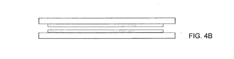
第二の基板の表面上に第二の光学材料を含む光学部品の実施形態の一例を、断面図にて図4Bに示す。量子閉じ込め半導体ナノ粒子は、電子および正孔を閉じ込めることができ、光を吸収して異なった波長の光を放出する光ルミネセンス性をもつ。量子閉じ込め半導体ナノ粒子からの放出光の色特性は、量子閉じ込め半導体ナノ粒子の大きさと量子閉じ込め半導体ナノ粒子の化学組成によって決まる。 An example of an embodiment of an optical component that includes a second optical material on the surface of a second substrate is shown in cross-sectional view in FIG. 4B. Quantum confined semiconductor nanoparticles can confine electrons and holes and have photoluminescence properties that absorb light and emit light of different wavelengths. The color characteristics of the emitted light from the quantum confined semiconductor nanoparticles are determined by the size of the quantum confined semiconductor nanoparticles and the chemical composition of the quantum confined semiconductor nanoparticles.
量子閉じ込め半導体ナノ粒子は、化学組成、構造および大きさについて少なくとも一タイプの量子閉じ込め半導体ナノ粒子を含む。本発明に係る光学部品の中に含まれる量子閉じ込め半導体ナノ粒子のタイプは、変換される光の波長と所望の光出力によって決まる。本明細書で検討されているように、量子閉じ込め半導体ナノ粒子は、粒子の表面にシェルおよび/またはリガンドを含んでいても含んでいなくてもよい。一定の実施形態において、シェルおよび/またはリガンドは、量子閉じ込め半導体ナノ粒子を不動態化して、凝集または集塊形成を防止して、ナノ粒子間のファンデルワールス結合力に打ち勝つことができる。一定の実施形態において、リガンドは、量子閉じ込め半導体ナノ粒子を含むことができる任意の母材に対して親和性をもつ材料を含んでいてもよい。本明細書で検討されているように、一定の実施形態において、シェルは無機シェルを含む。 Quantum confined semiconductor nanoparticles include at least one type of quantum confined semiconductor nanoparticles with respect to chemical composition, structure, and size. The type of quantum confined semiconductor nanoparticles contained in the optical component according to the present invention depends on the wavelength of light to be converted and the desired light output. As discussed herein, quantum confined semiconductor nanoparticles may or may not include a shell and / or ligand on the surface of the particle. In certain embodiments, the shell and / or ligand can passivate quantum confined semiconductor nanoparticles to prevent agglomeration or agglomeration and overcome van der Waals binding forces between the nanoparticles. In certain embodiments, the ligand may include a material that has an affinity for any matrix that can include quantum confined semiconductor nanoparticles. As discussed herein, in certain embodiments, the shell comprises an inorganic shell.
一定の実施形態において、光学材料の中に含まれる量子閉じ込め半導体ナノ粒子はカドミウムを含まない。 In certain embodiments, the quantum confined semiconductor nanoparticles included in the optical material do not include cadmium.
一定の実施形態において、光学材料の中に含まれる量子閉じ込め半導体ナノ粒子は、III−V半導体材料を含む。 In certain embodiments, the quantum confined semiconductor nanoparticles included in the optical material comprise a III-V semiconductor material.
一定の実施形態において、光学材料の中に含まれる量子閉じ込め半導体ナノ粒子は、半導体材料を含むコア、およびコアの表面の少なくとも一部の上に置かれた無機シェルを含む半導体ナノ結晶を含む。 In certain embodiments, quantum confined semiconductor nanoparticles included in an optical material include a semiconductor nanocrystal that includes a core that includes the semiconductor material and an inorganic shell that is disposed over at least a portion of the surface of the core.
量子閉じ込め半導体ナノ粒子は、本明細書において、「QD」という略称で呼ばれることもある。 Quantum confined semiconductor nanoparticles are sometimes referred to herein as the abbreviation “QD”.
一定の実施形態において、光学材料は、一つ以上の異なったタイプの量子閉じ込め半導体ナノ粒子(組成、構造および/またはサイズに基づく)を含み、各タイプは、所定の色をもつ光が得られるよう選択される。 In certain embodiments, the optical material comprises one or more different types of quantum confined semiconductor nanoparticles (based on composition, structure and / or size), each type providing light with a predetermined color. Selected.
一定の実施形態において、光学材料は、橙色から赤色のスペクトル領域(例えば約575nmから約650nm)で発光することができる量子閉じ込め半導体ナノ粒子を含むことができる。 In certain embodiments, the optical material can include quantum confined semiconductor nanoparticles that can emit in the orange to red spectral region (eg, from about 575 nm to about 650 nm).
一定の実施形態において、光学材料は、赤色スペクトル領域で発光することができる量子閉じ込め半導体ナノ粒子を含むことができる。 In certain embodiments, the optical material can include quantum confined semiconductor nanoparticles that can emit in the red spectral region.
一定の実施形態において、光学材料は、橙色スペクトル領域で発光することができる量子閉じ込め半導体ナノ粒子を含むことができる。 In certain embodiments, the optical material can include quantum confined semiconductor nanoparticles that can emit in the orange spectral region.
一定の実施形態において、光学材料は、シアン色スペクトル領域で発光することができる量子閉じ込め半導体ナノ粒子を含むことができる。 In certain embodiments, the optical material can include quantum confined semiconductor nanoparticles that can emit in the cyan spectral region.
一定の実施形態において、光学材料は、一つ以上の他の所定のスペクトル領域で発光することができる量子閉じ込め半導体ナノ粒子を含むことができる。 In certain embodiments, the optical material can include quantum confined semiconductor nanoparticles that can emit in one or more other predetermined spectral regions.
一定の実施形態において、光学材料の中に含まれる量子閉じ込め半導体ナノ粒子は、光学材料に含まれる前に少なくとも約60%、好ましくは少なくとも約70%、より好ましくは少なくとも約80%、最も好ましくは少なくとも約85%の溶液量子効率をもつ。 In certain embodiments, the quantum confined semiconductor nanoparticles included in the optical material are at least about 60%, preferably at least about 70%, more preferably at least about 80%, most preferably before being included in the optical material. It has a solution quantum efficiency of at least about 85%.
一定の実施形態において、光学部品は、一つ以上の異なったタイプの量子閉じ込め半導体ナノ粒子(組成、構造および/またはサイズ、またはナノ粒子に基づく)であって、各異なったタイプの量子閉じ込め半導体ナノ粒子が、光学材料に含まれる別のタイプの量子閉じ込め半導体ナノ粒子によって放出される所定の波長と同一であっても異なっていてもよい所定の波長の光を放出するナノ粒子を含む光学材料を含む。所定の波長は、光学部品の目的とする最終用途に基づいて選択される。2つ以上の異なったタイプの量子閉じ込め半導体ナノ粒子を含む一定の実施形態において、少なくとも2つのタイプが、該光学部品に含まれ得る、少なくとも一つの別のタイプの量子閉じ込め半導体ナノ粒子によって放出される波長とは異なった所定の波長の光を放出することができる。 In certain embodiments, the optical component is one or more different types of quantum confined semiconductor nanoparticles (based on composition, structure and / or size, or nanoparticles), each different type of quantum confined semiconductor An optical material comprising a nanoparticle that emits light of a predetermined wavelength that may be the same as or different from the predetermined wavelength emitted by another type of quantum confined semiconductor nanoparticles contained in the optical material including. The predetermined wavelength is selected based on the intended end use of the optical component. In certain embodiments comprising two or more different types of quantum confined semiconductor nanoparticles, at least two types are emitted by at least one other type of quantum confined semiconductor nanoparticles that can be included in the optical component. It is possible to emit light having a predetermined wavelength different from the wavelength to be transmitted.
異なった所定の波長を放出する2つ以上の異なったタイプの量子閉じ込め半導体ナノ粒子を含む一定の実施形態において、異なったタイプの量子閉じ込め半導体ナノ粒子は、一つ以上の異なった光学材料に含まれていてもよい。 In certain embodiments that include two or more different types of quantum confined semiconductor nanoparticles that emit different predetermined wavelengths, the different types of quantum confined semiconductor nanoparticles are included in one or more different optical materials. It may be.
異なった所定の波長を放出する2つ以上の異なったタイプの量子閉じ込め半導体ナノ粒子を含む一定の実施形態において、異なったタイプの量子閉じ込め半導体ナノ粒子は、2つ以上の異なった光学材料に含まれていてもよい。 In certain embodiments including two or more different types of quantum confined semiconductor nanoparticles that emit different predetermined wavelengths, the different types of quantum confined semiconductor nanoparticles are included in two or more different optical materials. It may be.
2つ以上の異なった光学材料を含む一定の実施形態において、このような異なった光学材料は、例えば、層状に配置された別々の層として、および/またはパターン層の別々のフィーチャとして含まれ得る。 In certain embodiments that include two or more different optical materials, such different optical materials can be included, for example, as separate layers arranged in layers and / or as separate features of a patterned layer. .
一定の実施形態において、例えば、所定の波長は、約470nmから約650nm、約580nmから約630nm、約590nmから約630nm、約590nmから約630nm、または約600nmから約620nm、約600から約610、または608から約618の範囲であってもよい。他の所定の波長が有用または所望されると判断され得る。 In certain embodiments, for example, the predetermined wavelength is about 470 nm to about 650 nm, about 580 nm to about 630 nm, about 590 nm to about 630 nm, about 590 nm to about 630 nm, or about 600 nm to about 620 nm, about 600 to about 610, Or it may range from 608 to about 618. It can be determined that other predetermined wavelengths are useful or desired.
一定の好適な実施形態において、量子閉じ込め半導体ナノ粒子は、半導体ナノ結晶を含む。 In certain preferred embodiments, the quantum confined semiconductor nanoparticles comprise semiconductor nanocrystals.
一定の実施形態において、光学材料中の量子閉じ込め半導体ナノ粒子は、少なくとも40%の固体光ルミネセンス量子効率をもつ。一定の実施形態において、光学材料中の量子閉じ込め半導体ナノ粒子は、少なくとも50%の固体光ルミネセンス量子効率をもつ。一定の実施形態において、光学材料中の量子閉じ込め半導体ナノ粒子は、少なくとも60%の固体光ルミネセンス量子効率をもつ。一定の実施形態において、光学材料中の量子閉じ込め半導体ナノ粒子は、少なくとも70%の固体光ルミネセンス量子効率をもつ。一定の実施形態において、光学材料中の量子閉じ込め半導体ナノ粒子は、少なくとも80%の固体光ルミネセンス量子効率をもつ。一定の実施形態において、光学材料中の量子閉じ込め半導体ナノ粒子は、少なくとも90%の固体光ルミネセンス量子効率をもつ。 In certain embodiments, the quantum confined semiconductor nanoparticles in the optical material have a solid state photoluminescence quantum efficiency of at least 40%. In certain embodiments, the quantum confined semiconductor nanoparticles in the optical material have a solid state photoluminescence quantum efficiency of at least 50%. In certain embodiments, the quantum confined semiconductor nanoparticles in the optical material have a solid state photoluminescence quantum efficiency of at least 60%. In certain embodiments, the quantum confined semiconductor nanoparticles in the optical material have a solid state photoluminescence quantum efficiency of at least 70%. In certain embodiments, the quantum confined semiconductor nanoparticles in the optical material have a solid state photoluminescence quantum efficiency of at least 80%. In certain embodiments, the quantum confined semiconductor nanoparticles in the optical material have a solid state photoluminescence quantum efficiency of at least 90%.
一定の好適な実施形態において、光学材料は、赤色光を放出することができる量子閉じ込め半導体ナノ粒子を含む。別の好適な実施形態において、光学材料は、橙色から赤色のスペクトル領域で光を放出することができる量子閉じ込め半導体ナノ粒子を含む。 In certain preferred embodiments, the optical material comprises quantum confined semiconductor nanoparticles capable of emitting red light. In another preferred embodiment, the optical material comprises quantum confined semiconductor nanoparticles capable of emitting light in the orange to red spectral region.
一定の実施形態において、光学材料は、母材に分布する量子閉じ込め半導体ナノ粒子を含む。 In certain embodiments, the optical material comprises quantum confined semiconductor nanoparticles distributed in the matrix.
一定の実施形態において、光学材料はさらに、量子閉じ込め半導体ナノ粒子が分布している母材を含む。一定の実施形態において、量子閉じ込め半導体ナノ粒子は、母材の重量の約0.001から約5重量パーセントまでの範囲の量で光学材料に含まれる。一定の実施形態において、光学材料は、母材の重量あたり約0.1から約3重量パーセントの量子閉じ込め半導体ナノ粒子を含む。一定の実施形態において、量子閉じ込め半導体ナノ粒子は、母材の重量の約0.5から約3重量パーセントまでの範囲の量で光学材料に含まれる。一定の実施形態において、量子閉じ込め半導体ナノ粒子は、母材の重量の約1から約3重量パーセントまでの範囲の量で光学材料に含まれる。一定の実施形態において、量子閉じ込め半導体ナノ粒子は、母材の重量の約1から約2重量パーセントまでの範囲の量で光学材料に含まれる。一定の実施形態において、量子閉じ込め半導体ナノ粒子は、母材の重量の約0.1から約1重量パーセントまでの範囲の量で光学材料に含まれる。一定の実施形態において、量子閉じ込め半導体ナノ粒子は、母材の重量の約0.1から約0.75重量パーセントまでの範囲の量で光学材料に含まれる。 In certain embodiments, the optical material further comprises a matrix in which the quantum confined semiconductor nanoparticles are distributed. In certain embodiments, the quantum confined semiconductor nanoparticles are included in the optical material in an amount ranging from about 0.001 to about 5 weight percent of the weight of the matrix. In certain embodiments, the optical material comprises about 0.1 to about 3 weight percent quantum confined semiconductor nanoparticles per weight of the matrix. In certain embodiments, the quantum confined semiconductor nanoparticles are included in the optical material in an amount ranging from about 0.5 to about 3 weight percent of the weight of the matrix. In certain embodiments, the quantum confined semiconductor nanoparticles are included in the optical material in an amount ranging from about 1 to about 3 weight percent of the weight of the matrix. In certain embodiments, the quantum confined semiconductor nanoparticles are included in the optical material in an amount ranging from about 1 to about 2 weight percent of the weight of the matrix. In certain embodiments, the quantum confined semiconductor nanoparticles are included in the optical material in an amount ranging from about 0.1 to about 1 weight percent of the weight of the matrix. In certain embodiments, the quantum confined semiconductor nanoparticles are included in the optical material in an amount ranging from about 0.1 to about 0.75 weight percent of the weight of the matrix.
母材をさらに含む光学材料の一定の実施形態において、量子閉じ込め半導体ナノ粒子は、母材の約5重量パーセントよりも多量に光学材料に含まれていてもよい。例えば、光学材料は、母材の重量あたり約5から約20重量パーセントの量子閉じ込め半導体ナノ粒子を含んでいてもよく、光学材料は、母材の重量あたり約5から約15重量パーセントの量子閉じ込め半導体ナノ粒子を含んでいてもよく、光学材料は、母材の重量あたり約5から約10重量パーセントの量子閉じ込め半導体ナノ粒子を含んでいてもよい。 In certain embodiments of the optical material further comprising a matrix, the quantum confined semiconductor nanoparticles may be included in the optical material in greater than about 5 weight percent of the matrix. For example, the optical material may include about 5 to about 20 weight percent quantum confined semiconductor nanoparticles per weight of the matrix, and the optical material includes about 5 to about 15 weight percent quantum confinement per weight of the matrix. The semiconductor material may include semiconductor nanoparticles and the optical material may include from about 5 to about 10 weight percent quantum confined semiconductor nanoparticles per weight of the matrix.
光学材料における上記範囲以外の濃度の量子閉じ込め半導体ナノ粒子であっても、有用または所望であると判断され得る。 Even quantum confined semiconductor nanoparticles in concentrations other than the above ranges in optical materials may be deemed useful or desirable.
好ましくは、母材は、固体の母材を含む。本明細書に記載された本発明の様々な実施形態および態様において有用な母材の例は、ポリマー、モノマー、樹脂、結合剤、ガラス、金属酸化物、および他の非高分子物質などである。好適な母材は、所定の波長の光に対し光学的に透明な高分子物質または非高分子物質などである。 Preferably, the base material includes a solid base material. Examples of matrices useful in the various embodiments and aspects of the invention described herein are polymers, monomers, resins, binders, glasses, metal oxides, and other non-polymeric materials. . A suitable base material is a polymer material or non-polymer material that is optically transparent to light of a predetermined wavelength.
一定の実施形態において、母材は、光学部品を出入りする、少なくとも所定の波長の光に対し少なくとも90%光学的に透明である。一定の実施形態において、母材は、光学部品を出入りする、少なくとも所定の波長の光に対し少なくとも95%光学的に透明である。一定の実施形態において、母材は、光学部品を出入りする、少なくとも所定の波長の光に対し少なくとも99%光学的に透明である。 In certain embodiments, the matrix is at least 90% optically transparent to at least a predetermined wavelength of light entering and exiting the optical component. In certain embodiments, the matrix is at least 95% optically transparent to at least a predetermined wavelength of light entering and exiting the optical component. In certain embodiments, the matrix is at least 99% optically transparent to at least a predetermined wavelength of light entering and exiting the optical component.
一定の実施形態において、所定の波長は、電磁スペクトルの可視(例えば400から700nm)領域の波長の光を含んでいてもよい。 In certain embodiments, the predetermined wavelength may include light of a wavelength in the visible (eg, 400 to 700 nm) region of the electromagnetic spectrum.
好適な母材は、架橋ポリマーおよび溶媒キャストポリマーなどである。好適な母材の例は、少なくとも所定の波長の光に対し光学的に透明なガラスまたは樹脂であるが、これらに限定されない。特に、非硬化性樹脂、熱硬化性樹脂または光硬化性樹脂などの樹脂が、加工性の観点から適切に使用される。このような樹脂の具体例は、オリゴマーまたはポリマーいずれかの形状のメラミン樹脂、フェノール樹脂、アルキル樹脂、エポキシ樹脂、ポリウレタン樹脂、マレイン酸樹脂、ポリアミド樹脂、ポリメチルメタクリル酸、ポリアクリル酸、ポリカーボナート、ポリビニル・アルコール、ポリビニルピロリドン、ヒドロキシエチルセルロース、カルボキシメチルセルロース、これらの樹脂を形成するモノマーを含むコポリマーなどである。この他の適切な母材は、関連技術分野の当業者によって確認可能である。 Suitable base materials include crosslinked polymers and solvent cast polymers. An example of a suitable base material is glass or resin that is optically transparent to light of at least a predetermined wavelength, but is not limited thereto. In particular, a resin such as a non-curable resin, a thermosetting resin, or a photocurable resin is appropriately used from the viewpoint of workability. Specific examples of such resins are melamine resins in the form of oligomers or polymers, phenol resins, alkyl resins, epoxy resins, polyurethane resins, maleic resins, polyamide resins, polymethylmethacrylic acid, polyacrylic acid, polycarbonate , Polyvinyl alcohol, polyvinyl pyrrolidone, hydroxyethyl cellulose, carboxymethyl cellulose, and copolymers containing monomers that form these resins. Other suitable base materials can be ascertained by one skilled in the relevant art.
本開示によって想定される発明の一定の実施形態および態様において、母材は光硬化性樹脂である。光硬化性樹脂は、一定の実施形態、例えば、組成物がパターン化される実施形態においては好適な母材であろう。光硬化性樹脂としては、光重合性樹脂、例えば、アクリル酸またはメタクリル酸を原料とし、反応性ビニル基を含有する樹脂、光増感剤を通常含有する光架橋性樹脂、例えばポリビニルシンナマート、ベンゾフェノンなどを使用することができる。光増感剤を用いない場合には熱硬化性樹脂を使用することができる。これらの樹脂は、個別に、または2つ以上を組み合わせて使用することができる。 In certain embodiments and aspects of the invention envisioned by this disclosure, the matrix is a photocurable resin. The photocurable resin may be a suitable matrix in certain embodiments, for example, embodiments in which the composition is patterned. As the photocurable resin, a photopolymerizable resin, for example, acrylic acid or methacrylic acid as a raw material, a resin containing a reactive vinyl group, a photocrosslinkable resin usually containing a photosensitizer, such as polyvinyl cinnamate, Benzophenone or the like can be used. When no photosensitizer is used, a thermosetting resin can be used. These resins can be used individually or in combination of two or more.
本開示によって想定される発明の一定の実施形態および態様において、母材は溶媒キャスト樹脂を含む。ポリウレタン樹脂、マレイン酸樹脂、ポリアミド樹脂、ポリメチルメタクリル酸、ポリアクリル酸、ポリカーボナート、ポリビニル・アルコール、ポリビニルピロリドン、ヒドロキシエチルセルロース、カルボキシメチルセルロース、これらの樹脂を形成するモノマーを含むコポリマーなどの樹脂は、当業者に既知の溶媒に溶解させることができる。溶媒を蒸発させると、樹脂は、半導体ナノ粒子用の固体の母材を形成する。 In certain embodiments and aspects of the invention contemplated by this disclosure, the matrix includes a solvent cast resin. Resins such as polyurethane resins, maleic resins, polyamide resins, polymethyl methacrylic acid, polyacrylic acid, polycarbonate, polyvinyl alcohol, polyvinyl pyrrolidone, hydroxyethyl cellulose, carboxymethyl cellulose, copolymers containing monomers that form these resins, It can be dissolved in a solvent known to those skilled in the art. When the solvent is evaporated, the resin forms a solid matrix for the semiconductor nanoparticles.
一定の実施形態において、光散乱体が光学材料に含まれる。一定の実施形態において、光散乱体は光散乱粒子を含む。一定の実施形態において、光散乱粒子は、母材の重量の約0.001から約5重量パーセントまでの範囲の量で光学材料に含まれる。一定の実施形態において、光散乱粒子は、母材の重量の約0.5から約3重量パーセントまでの範囲の量で光学材料に含まれる。一定の実施形態において、光散乱粒子は、母材の重量の約1から約3重量パーセントまでの範囲の量で光学材料に含まれる。一定の実施形態において、光散乱粒子は、母材の重量の約1から約2重量パーセントまでの範囲の量で光学材料に含まれる。一定の実施形態において、光散乱粒子は、母材の重量の約0.05から約1重量パーセントまでの範囲の量で光学材料に含まれる。 In certain embodiments, light scatterers are included in the optical material. In certain embodiments, the light scatterer comprises light scattering particles. In certain embodiments, light scattering particles are included in the optical material in an amount ranging from about 0.001 to about 5 weight percent of the weight of the matrix. In certain embodiments, the light scattering particles are included in the optical material in an amount ranging from about 0.5 to about 3 weight percent of the weight of the matrix. In certain embodiments, the light scattering particles are included in the optical material in an amount ranging from about 1 to about 3 weight percent of the weight of the matrix. In certain embodiments, the light scattering particles are included in the optical material in an amount ranging from about 1 to about 2 weight percent of the weight of the matrix. In certain embodiments, the light scattering particles are included in the optical material in an amount ranging from about 0.05 to about 1 weight percent of the weight of the matrix.
一定の実施形態において、光散乱粒子は、母材の約5重量パーセントよりも多量に光学材料に含まれる。例えば、光学材料は、母材の重量あたり約5から約20重量パーセントの光散乱粒子を含んでいてもよく、光学材料は、母材の重量あたり約5から約15重量パーセントの光散乱粒子を含んでいてもよく、光学材料は、母材の重量あたり約5から約10重量パーセントの光散乱粒子を含んでいてもよいなどである。 In certain embodiments, the light scattering particles are included in the optical material in greater than about 5 weight percent of the matrix. For example, the optical material may include about 5 to about 20 weight percent light scattering particles per weight of the matrix, and the optical material includes about 5 to about 15 weight percent light scattering particles per weight of the matrix. The optical material may include from about 5 to about 10 weight percent light scattering particles per weight of the matrix, and so forth.
光学材料における上記範囲以外の濃度の光散乱粒子であっても、有用または所望であると判断され得る。 Even light scattering particles having a concentration outside the above range in the optical material may be judged useful or desirable.
一定の実施形態において、量子閉じ込め半導体ナノ粒子と散乱体の重量比は約1:100から100:1である。 In certain embodiments, the weight ratio of quantum confined semiconductor nanoparticles to scatterers is about 1: 100 to 100: 1.
本明細書記載の発明の実施形態および態様において使用することができる光散乱体(本明細書では、散乱体または光散乱粒子とも呼ばれている)の例は、金属もしくは金属酸化物、空気泡、ならびにガラスおよび高分子のビーズ(固体または中空)などであるが、これらに限定されない。この他の散乱体は、当業者によって容易に確認することができる。一定の実施形態において、散乱体は球形である。光散乱粒子の好適例は、TiO2、SiO2、BaTiO3、BaSO4およびZnOなどであるが、これらに限定されない。母材と非反応性で、母材における励起光の吸収経路長を増加させることができる、他の材料の粒子を使用することもできる。一定の実施形態において、光散乱体は、高い屈折率をもっていること(例えばTiO2、BaSO4など)または低い屈折率をもっていること(気泡)が可能である。一定の好適な実施形態において、光散乱体は発光性ではない。 Examples of light scatterers (also referred to herein as scatterers or light scattering particles) that can be used in the embodiments and aspects of the invention described herein include metals or metal oxides, air bubbles , And glass and polymer beads (solid or hollow), but are not limited to these. Other scatterers can be easily identified by those skilled in the art. In certain embodiments, the scatterer is spherical. Preferable examples of the light scattering particles include TiO 2 , SiO 2 , BaTiO 3 , BaSO 4, and ZnO, but are not limited thereto. Particles of other materials that are non-reactive with the matrix and can increase the absorption path length of the excitation light in the matrix can also be used. In certain embodiments, the light scatterer can have a high refractive index (eg, TiO 2 , BaSO 4, etc.) or a low refractive index (bubbles). In certain preferred embodiments, the light scatterers are not luminescent.
散乱体のサイズとサイズ分布の選択は、当業者によって容易に決定可能である。サイズとサイズ分布は、散乱粒子と、中に光散乱体を分散させる母材との屈折率の不整合や、レイリーの散乱理論に従って散乱させるために予め選択された波長に基づいていてもよい。散乱粒子の表面をさらに処理して、母材の分散性と安定性を向上させることができる。一つの実施形態において、散乱粒子は、中央粒径0.405ミクロンのTiO2(デュポン社(DuPont)のR902+)を約0.001から約5重量%の濃度で含む。一定の好適な実施形態において、散乱体の濃度範囲は0.05重量%から2重量%の間である。 The choice of scatterer size and size distribution can be readily determined by one skilled in the art. The size and size distribution may be based on a refractive index mismatch between the scattering particles and the matrix within which the light scatterers are dispersed, or on wavelengths preselected for scattering according to Rayleigh scattering theory. The surface of the scattering particles can be further processed to improve the dispersibility and stability of the matrix. In one embodiment, the scattering particles comprise TiO 2 (DuPont R902 +) with a median particle size of 0.405 microns at a concentration of about 0.001 to about 5% by weight. In certain preferred embodiments, the scatterer concentration range is between 0.05 wt% and 2 wt%.
一定の実施形態において、量子閉じ込め半導体ナノ粒子と母材を含む光学材料を、量子閉じ込め半導体ナノ粒子と、架橋され得る一つ以上の官能基を含む組成物を含む液体溶媒とを含むインクから形成することができる。官能単位は、例えば、UV処理、熱処理、または当業者によって容易に確認することができる別の架橋技術によって架橋することができる。一定の実施形態において、架橋され得る一つ以上の官能基を含む組成物は、液体溶媒そのものであってもよい。一定の実施形態において、これは共溶媒であってもよい。一定の実施形態において、これは液体溶媒との混合物の成分であってもよい。一定の実施形態において、インクはさらに光散乱体を含んでいてもよい。さらに、光学材料に含まれ得る他の添加剤および/または成分をインクに含ませることができる。 In certain embodiments, an optical material comprising quantum confined semiconductor nanoparticles and a matrix is formed from an ink comprising quantum confined semiconductor nanoparticles and a liquid solvent comprising a composition comprising one or more functional groups that can be cross-linked. can do. The functional units can be crosslinked, for example, by UV treatment, heat treatment, or another crosslinking technique that can be readily ascertained by one skilled in the art. In certain embodiments, the composition comprising one or more functional groups that can be crosslinked may be the liquid solvent itself. In certain embodiments, this may be a co-solvent. In certain embodiments, this may be a component of a mixture with a liquid solvent. In certain embodiments, the ink may further include a light scatterer. In addition, other additives and / or components that may be included in the optical material can be included in the ink.
本開示によって想定された発明の一定の好適な実施形態において、量子閉じ込め半導体ナノ粒子(例えば、半導体ナノ結晶)を個別の粒子として光学材料の内部に分布させている。 In certain preferred embodiments of the invention envisioned by this disclosure, quantum confined semiconductor nanoparticles (eg, semiconductor nanocrystals) are distributed as individual particles within the optical material.
一定の実施形態において、光学材料は、他の添加剤(例えば、湿潤剤またはレベリング剤)も含むことができる。 In certain embodiments, the optical material can also include other additives (eg, wetting agents or leveling agents).
本明細書で教示されている発明の一定の態様および実施形態において、光学部品は、第一の光学的に透明な基板および第二の光学的に透明な基板を含む。 In certain aspects and embodiments of the invention taught herein, the optical component includes a first optically transparent substrate and a second optically transparent substrate.
一定の実施形態において、基板の一方または両方は、光学部品を出入りする、少なくとも所定の波長の光に対し80%光学的に透明である。一定の実施形態において、基板の一方または両方は、光学部品を出入りする、少なくとも所定の波長の光に対し少なくとも85%光学的に透明である。一定の実施形態において、基板の一方または両方は、光学部品を出入りする、少なくとも所定の波長の光に対し少なくとも90%光学的に透明である。一定の実施形態において、基板の一方または両方は、光学部品を出入りする、少なくとも所定の波長の光に対し少なくとも95%光学的に透明である。一定の実施形態において、基板の一方または両方は、光学部品を出入りする、少なくとも所定の波長の光に対し少なくとも99%光学的に透明である。 In certain embodiments, one or both of the substrates are 80% optically transparent to at least a predetermined wavelength of light entering and exiting the optical component. In certain embodiments, one or both of the substrates are at least 85% optically transparent to at least a predetermined wavelength of light entering and exiting the optical component. In certain embodiments, one or both of the substrates are at least 90% optically transparent to at least a predetermined wavelength of light entering and exiting the optical component. In certain embodiments, one or both of the substrates is at least 95% optically transparent to at least a predetermined wavelength of light entering and exiting the optical component. In certain embodiments, one or both of the substrates are at least 99% optically transparent to at least a predetermined wavelength of light entering and exiting the optical component.
一定の実施形態において、基板の一方または両方は、剛性の材料、例えば、ガラス、ポリカーボナート、アクリル、クォーツ、サファイア、または他の既知の剛性材料を含んでいてもよい。 In certain embodiments, one or both of the substrates may include a rigid material, such as glass, polycarbonate, acrylic, quartz, sapphire, or other known rigid materials.
一定の実施形態において、基板の一方または両方は、可塑性の材料、例えば、プラスチック(例えば薄いアクリル、エポキシ、ポリカーボナート、PEN、PET、PEであるが、これらに限定されない)やシリコンなどの高分子材料を含んでいてもよい。 In certain embodiments, one or both of the substrates is a plastic material, for example, a polymer such as plastic (eg, but not limited to thin acrylic, epoxy, polycarbonate, PEN, PET, PE) or silicon. It may contain material.
一定の実施形態において、基板の一方または両方は、シリカまたは基板の上のガラスコーティングを含む可塑性材料を含んでいてもよい。好ましくは、シリカまたはガラスコーティングは、可塑性基材の可塑性を保持するのに十分な薄さである。 In certain embodiments, one or both of the substrates may include a plastic material that includes silica or a glass coating on the substrate. Preferably, the silica or glass coating is thin enough to retain the plasticity of the plastic substrate.
一定の実施形態において、基板は同じものである。 In certain embodiments, the substrates are the same.
一定の実施形態において、各基板は異なっている。 In certain embodiments, each substrate is different.
一定の実施形態において、基板の一方または両方は、約0.1%から約5%の範囲にある透過ヘイズ(ASTM D1003−0095に定義されている)を含んでいてもよい。(ASTM D1003−0095は参照することにより本明細書に組み込まれる。)一定の実施形態において、基板の一方または両方の主表面の一方または両方は平滑である。 In certain embodiments, one or both of the substrates may include transmission haze (as defined in ASTM D1003-0095) in the range of about 0.1% to about 5%. (ASTM D1003-0095 is incorporated herein by reference.) In certain embodiments, one or both major surfaces of one or both of the substrates are smooth.
一定の実施形態において、光学材料と接着層が間に置かれている基板表面の少なくとも一方、好ましくは両方とも非平滑である。このような実施形態の一部において、このような基板表面の一方または両方はざらつきがある。このような実施形態の一部において、このような基板表面の一方または両方は粗面になっている。このような実施形態の一部において、このような基板表面の一方または両方はエッチングされている。 In certain embodiments, at least one, and preferably both, of the substrate surface between which the optical material and the adhesive layer are interposed are non-smooth. In some such embodiments, one or both of the substrate surfaces is rough. In some of such embodiments, one or both of the substrate surfaces is rough. In some such embodiments, one or both of such substrate surfaces are etched.
一定の好適な実施形態において、このような非平滑基板表面の一方または両方は、1000オングストロームよりも大きい表面粗さ(Ra−算術平均プロファイル粗さパラメータ)をもつ。 In certain preferred embodiments, one or both of such non-smooth substrate surfaces has a surface roughness (Ra-arithmetic average profile roughness parameter) greater than 1000 angstroms.
一定の実施形態において、非平滑面は、基板を完全には覆っていないが、標準的な方法(例えば、マスキングまたは選択的粗化、エッチング、テクスチャ化など)によってパターン化されている。 In certain embodiments, the non-smooth surface does not completely cover the substrate, but is patterned by standard methods (eg, masking or selective roughening, etching, texturing, etc.).
一定の実施形態において、基板の一方または両方の主表面の一方または両方は波形であってもよい。 In certain embodiments, one or both major surfaces of one or both of the substrates may be corrugated.
一定の実施形態において、基板の一方または両方の主表面の一方または両方は粗面になっていてもよい。 In certain embodiments, one or both major surfaces of one or both of the substrates may be rough.
一定の実施形態において、基板の一方または両方の主表面の一方または両方はざらつきがあってもよい。 In certain embodiments, one or both major surfaces of one or both of the substrates may be rough.
一定の実施形態において、基板の一方または両方の主表面の一方または両方は凹状であってもよい。 In certain embodiments, one or both major surfaces of one or both of the substrates may be concave.
一定の実施形態において、基板の一方または両方の主表面の一方または両方は凸状であってもよい。 In certain embodiments, one or both major surfaces of one or both of the substrates may be convex.
一定の実施形態において、基板の少なくとも一つの一つ主表面がマイクロレンズを含んでいてもよい。 In certain embodiments, at least one major surface of the substrate may include microlenses.
一定の実施形態において、基板の一方または両方の厚さは実質的に均一である。 In certain embodiments, the thickness of one or both of the substrates is substantially uniform.
一定の実施形態において、光学材料および接着剤が間に置かれている基板の表面の一方または両方は滑らかである。このような実施形態の一部において、このような滑らかな基板表面の少なくとも一方、好ましくは両方の水接触角は、空気−基板界面において40°以下、好ましくは25°以下、およびより好ましくは15°以下である。 In certain embodiments, one or both of the surfaces of the substrate between which the optical material and adhesive are placed are smooth. In some of such embodiments, the water contact angle of at least one of such smooth substrate surfaces, preferably both, is 40 ° or less, preferably 25 ° or less, and more preferably 15 at the air-substrate interface. ° or less.
一定の実施形態において、第一の基板および第二の基板の幾何学的形状および寸法は、具体的な最終用途に基づいて選択される(例えば、ランプ、固体照明装置、照明器具、または他の装置もしくは器具)。 In certain embodiments, the geometry and dimensions of the first substrate and the second substrate are selected based on the specific end use (eg, lamp, solid state lighting device, luminaire, or other Device or instrument).
一定の実施形態において、光学部品は、量子閉じ込め半導体ナノ粒子を含む一つ以上の光学材料を含む、少なくとも一つの層を含む。 In certain embodiments, the optical component includes at least one layer that includes one or more optical materials including quantum confined semiconductor nanoparticles.
一つよりも多くのタイプの量子閉じ込め半導体ナノ粒子を含む一定の実施形態において、各タイプが別々の層に含まれていてもよい。 In certain embodiments that include more than one type of quantum confined semiconductor nanoparticles, each type may be included in a separate layer.
一定の実施形態において、光学材料は、基板の主表面の全域に置かれている。 In certain embodiments, the optical material is placed throughout the major surface of the substrate.
一定の実施形態において、光学材料は、基板の主表面の全域に不断の層として置かれている。 In certain embodiments, the optical material is placed as a continuous layer across the major surface of the substrate.
本明細書に記載されているように、一定の実施形態において、光学材料を、パターン化されていてもパターン化されていなくてもよい所定の配置に置くことができる。 As described herein, in certain embodiments, the optical material can be placed in a predetermined arrangement that may or may not be patterned.
一定の実施形態において、光学材料は、基板の表面の所定の領域上に一つ以上の発光層として置かれる。 In certain embodiments, the optical material is placed as one or more emissive layers on a predetermined area of the surface of the substrate.
一定の実施形態において、母材を含む光学材料を含む層は、例えば、約0.1ミクロンから約1cmの厚さである。一定の実施形態において、母材を含む光学材料を含む層は、約0.1から約200ミクロンの厚さである。一定の実施形態において、母材を含む光学材料を含む層は、約10から約200ミクロンの厚さである。一定の実施形態において、母材を含む光学材料を含む層は、約30から約80ミクロンの厚さである。これら以外の厚さを有用または所望であると判断することも可能である。 In certain embodiments, the layer comprising the optical material including the matrix is, for example, about 0.1 microns to about 1 cm thick. In certain embodiments, the layer that includes the optical material, including the matrix, is about 0.1 to about 200 microns thick. In certain embodiments, the layer comprising the optical material including the matrix is about 10 to about 200 microns thick. In certain embodiments, the layer comprising the optical material including the matrix is about 30 to about 80 microns thick. It is also possible to determine that other thicknesses are useful or desired.
一定の実施形態において、この他の光学層を含むことも可能である。 In certain embodiments, other optical layers may be included.
一定の実施形態において、一つの層が2つ以上の層を含んでいてもよい。 In certain embodiments, a single layer may include more than one layer.
エネルギのことを考えると、さらにフィルタを含むことは望ましくない可能性があるが、別の理由でフィルタが含まれる事例もあり得る。このような場合には、フィルタを含むことも可能である。一定の実施形態において、フィルタは、支持要素の全部または少なくとも所定の一部を覆うことができる。一定の実施形態において、フィルタは、一つ以上の所定の波長の光の通過を遮断するために含まれていてもよい。フィルタ層は、光学材料の上または下に含まれていてもよい。一定の実施形態において、光学部品は、支持要素の様々な表面に複数のフィルタ層を含むことができる。一定の実施形態において、ノッチフィルタ層が含まれていてもよい。 Considering energy, it may not be desirable to include additional filters, but there may be cases where filters are included for other reasons. In such a case, a filter can be included. In certain embodiments, the filter can cover all or at least a predetermined portion of the support element. In certain embodiments, a filter may be included to block the passage of one or more predetermined wavelengths of light. The filter layer may be included above or below the optical material. In certain embodiments, the optical component can include multiple filter layers on various surfaces of the support element. In certain embodiments, a notch filter layer may be included.
一定の実施形態において、一つ以上の反射防止膜が光学部品に含まれていてもよい。 In certain embodiments, one or more anti-reflective coatings may be included in the optical component.
一定の実施形態において、一つ以上の波長選択性反射被膜が光学部品に含まれていてもよい。このような被膜は、例えば、光を光源に向かって戻すことができる。 In certain embodiments, one or more wavelength selective reflective coatings may be included in the optical component. Such a coating can, for example, return light toward the light source.
一定の実施形態において、例えば、光学部品は、さらに、表面の少なくとも一部を横切って出力結合用の部材または構造物を含むことができる。一定の実施形態において、出力結合用の部材または構造物は、表面の全域に均一に分布させることができる。一定の実施形態において、出力結合用の部材または構造物の形状、サイズおよび/または頻度は、表面から出力結合される光の分布をより均一にするために異なっていてもよい。一定の実施形態において、出力結合用の部材または構造物は、凸状、例えば、光学部品の表面上に乗っているか突き出していてもよく、または凹状、例えば、光学部品の表面で窪みになっていてもよく、または両方を組み合わせたものであってもよい。 In certain embodiments, for example, the optical component can further include an output coupling member or structure across at least a portion of the surface. In certain embodiments, the power coupling members or structures can be evenly distributed across the surface. In certain embodiments, the shape, size and / or frequency of the power coupling member or structure may be different to make the distribution of light coupled out from the surface more uniform. In certain embodiments, the output coupling member or structure may be convex, e.g. resting on or protruding from the surface of the optical component, or concave, e.g. recessed at the surface of the optical component. Or a combination of both.
一定の実施形態において、光学部品は、光が放出される表面上にレンズ、角柱面、格子などを含んでいてもよい。他のコーティングも場合によりこのような表面に含むことができる。 In certain embodiments, the optical component may include a lens, prismatic surface, grating, etc. on the surface from which light is emitted. Other coatings can optionally be included on such surfaces.
一定の実施形態において、出力結合用の部材または構造物は、型打ち、エンボス加工、ラミネート加工、硬化性調合剤の適用(例えば、吹付け、リソグラフィ、印刷(スクリーン、インクジェット、フレキソ印刷など)などであるが、これらに限定されない技術によって形成される)によって形成することができる。 In certain embodiments, the output coupling member or structure is stamped, embossed, laminated, applied with a curable formulation (eg, spraying, lithography, printing (screen, ink jet, flexographic printing, etc.), etc. However, it is formed by a technique not limited thereto).
一定の実施形態において、基板の一方または両方は、光散乱体を含んでいてもよい。 In certain embodiments, one or both of the substrates may include light scatterers.
一定の実施形態において、基板の一方または両方は、空気泡または空隙を含んでいてもよい。 In certain embodiments, one or both of the substrates may include air bubbles or voids.
一定の実施形態において、光学部品は、平面仕上げまたはつや消し仕上げをした一つ以上の主表面を含んでいてもよい。 In certain embodiments, the optical component may include one or more major surfaces with a flat or matte finish.
一定の実施形態において、光学部品は、つや出し仕上げをした一つ以上の表面を含んでいてもよい。 In certain embodiments, the optical component may include one or more surfaces that are polished.
本明細書に教示された発明の一定の態様および実施形態において、光学部品は場合により、環境(例えば、埃、湿気など)および/または引っかき傷や摩耗から保護するために、該部品の外側表面の全部または一部の上にカバー、膜または層をさらに含んでいてもよい。 In certain aspects and embodiments of the invention taught herein, the optical component optionally has an outer surface of the component to protect it from the environment (eg, dust, moisture, etc.) and / or scratches and wear. Further, a cover, a film or a layer may be further included on all or a part of.
接着材料は、好ましくは光透過特性および接着品質で選択される。 The adhesive material is preferably selected for light transmission properties and adhesion quality.
一定の好適な実施形態において、接着材料は、光学部品を出入りする、少なくとも所定の波長の光に対して光学的に透明である。 In certain preferred embodiments, the adhesive material is optically transparent to at least a predetermined wavelength of light entering and exiting the optical component.
一定の実施形態において、接着材料は、光学部品を出入りする、少なくとも所定の波長の光に対して少なくとも80%光学的に透明である。一定の実施形態において、接着材料は、光学部品を出入りする、少なくとも所定の波長の光に対して少なくとも85%光学的に透明である。一定の実施形態において、接着材料は、光学部品を出入りする、少なくとも所定の波長の光に対して少なくとも90%光学的に透明である。一定の実施形態において、接着材料は、光学部品を出入りする、少なくとも所定の波長の光に対して少なくとも95%光学的に透明である。一定の実施形態において、接着材料は、光学部品を出入りする、少なくとも所定の波長の光に対して少なくとも99%光学的に透明である。 In certain embodiments, the adhesive material is at least 80% optically transparent to at least a predetermined wavelength of light entering and exiting the optical component. In certain embodiments, the adhesive material is at least 85% optically transparent to at least a predetermined wavelength of light entering and exiting the optical component. In certain embodiments, the adhesive material is at least 90% optically transparent to at least a predetermined wavelength of light entering and exiting the optical component. In certain embodiments, the adhesive material is at least 95% optically transparent to at least a predetermined wavelength of light entering and exiting the optical component. In certain embodiments, the adhesive material is at least 99% optically transparent to at least a predetermined wavelength of light entering and exiting the optical component.
一定の好適な実施形態において、接着材料は、密閉している間に黄ばむことも変色することもない。より好ましくは、接着材料は、光学部品の有用耐用期間内に黄ばんだり変色したりして、光学部品の光学特性を実質的に変えることはない。 In certain preferred embodiments, the adhesive material does not yellow or change color while sealed. More preferably, the adhesive material does not yellow or change color within the useful life of the optical component to substantially change the optical properties of the optical component.
一定の好適な実施形態において、接着材料は、光学部品を一緒に密閉するのに適した接着特性をもつ。より好ましくは、シールは、光学部品の有用耐用期間内に一部または全部が薄い層に裂けたり、そうでなければ機能しなくなったりすることはない。 In certain preferred embodiments, the adhesive material has adhesive properties suitable for sealing the optical components together. More preferably, the seal does not rupture partly or completely into a thin layer or otherwise fail within the useful life of the optical component.
一定の好適な実施形態において、接着材料の性質は、光学材料の固体光ルミネセンス量子効率に対して最小限の影響しか与えない。 In certain preferred embodiments, the nature of the adhesive material has a minimal effect on the solid state photoluminescence quantum efficiency of the optical material.
一定の好適な実施形態において、接着材料は酸素障壁特性をもつ。 In certain preferred embodiments, the adhesive material has oxygen barrier properties.
一定の好適な実施形態において、接着材料は酸素障壁特性および防湿特性をもつ。 In certain preferred embodiments, the adhesive material has oxygen barrier properties and moisture barrier properties.
一定の好適な実施形態において、接着材料は、光学材料および光学材料の外部量子効率に悪影響を与えない条件下で硬くする(例えば硬化または乾燥させる)ことができる。好ましくは、接着材料はUV硬化させることができる。 In certain preferred embodiments, the adhesive material can be hardened (eg, cured or dried) under conditions that do not adversely affect the optical material and the external quantum efficiency of the optical material. Preferably, the adhesive material can be UV cured.
好ましくは、接着材料は、層を形成するに際して、光学材料上に分注された後も、最小限の落ち込みで盛り上がった状態として残る程度の粘度をもつ。この粘度特性によって、基板の間にある物質が、裸眼で観察できる気泡を実質的に含むことがなく、および好ましくは、含むことがなくなる光学部品を得ることを容易にする。好適な接着材料はUV硬化性アクリル系ウレタンである。UV硬化型アクリル系ウレタンの例は、Norland光学接着剤68およびNorland光学接着剤68Tという名のNorland Adhesives社によって販売されている製品などである。 Preferably, the adhesive material has a viscosity sufficient to remain as a raised state with minimal depression after being dispensed onto the optical material in forming the layer. This viscosity property facilitates obtaining an optical component in which the material between the substrates is substantially free of, and preferably free of, bubbles that can be observed with the naked eye. A preferred adhesive material is UV curable acrylic urethane. Examples of UV curable acrylic urethanes include products sold by Norland Adhesives under the name Norland optical adhesive 68 and Norland optical adhesive 68T.
一定の実施形態において、接着材料は、感圧接着剤を含んでいてもよい。 In certain embodiments, the adhesive material may include a pressure sensitive adhesive.
さらなる適切な接着材料(例えば、エポキシ類、アクリル類、ウレタン類、他のUV硬化型アクリル類など)を、関連技術分野の当業者によって容易に確認することができる。 Further suitable adhesive materials (eg, epoxies, acrylics, urethanes, other UV curable acrylics, etc.) can be readily ascertained by those skilled in the relevant art.
一定の実施形態において、光学部品はさらに、一つ以上の別々の障壁層を含んでいてもよい。例えば、光学材料を付着させる前に別々の障壁層を基板の表面に適用し、および/または、接着材料と接触させる前に、別々の障壁層を光学材料の上に適用することもできる。障壁材料は、実質的に酸素を通さない材料である。一定の実施形態において、障壁層は、実質的に酸素および水を通さない。 In certain embodiments, the optical component may further include one or more separate barrier layers. For example, a separate barrier layer can be applied to the surface of the substrate prior to depositing the optical material and / or a separate barrier layer can be applied over the optical material prior to contacting the adhesive material. The barrier material is a material that is substantially impermeable to oxygen. In certain embodiments, the barrier layer is substantially impermeable to oxygen and water.
適切な障壁用のフィルムまたは膜の例は、金属酸化物コーティング、薄いガラス層およびVitex Systems,Inc.から入手できるBarixコーティング材料を含むが、これらに限定されない。この他の障壁用のフィルムまたは膜は、当業者によって容易に確認することができる。 Examples of suitable barrier films or membranes include metal oxide coatings, thin glass layers, and Vitex Systems, Inc. Including, but not limited to, Barix coating materials available from: Other barrier films or membranes can be readily identified by those skilled in the art.
一定の実施形態において、一つ以上の障壁用のフィルムまたは膜を用いて、基板の間に光学材料をさらに封入することができる。 In certain embodiments, one or more barrier films or membranes can be used to further encapsulate the optical material between the substrates.
一定の好適な実施形態において、障壁材料は、少なくとも光学部品を出入りする光の所定の波長をもつ光に対して光学的に透明である。一定の実施形態において、障壁材料は、光学部品を出入りする所定の波長の光に対して少なくとも80%光学的に透明である。一定の実施形態において、障壁材料は、光学部品を出入りする所定の波長の光に対して少なくとも85%光学的に透明である。一定の実施形態において、障壁材料は、光学部品を出入りする所定の波長の光に対して少なくとも90%光学的に透明である。一定の実施形態において、障壁材料は、光学部品を出入りする所定の波長の光に対して少なくとも95%光学的に透明である。一定の実施形態において、障壁材料は、光学部品を出入りする所定の波長の光に対して少なくとも99%光学的に透明である。 In certain preferred embodiments, the barrier material is optically transparent to light having a predetermined wavelength of light entering and exiting the optical component. In certain embodiments, the barrier material is at least 80% optically transparent to light of a predetermined wavelength entering and exiting the optical component. In certain embodiments, the barrier material is at least 85% optically transparent to light of a predetermined wavelength entering and exiting the optical component. In certain embodiments, the barrier material is at least 90% optically transparent to light of a predetermined wavelength entering and exiting the optical component. In certain embodiments, the barrier material is at least 95% optically transparent to light of a predetermined wavelength entering and exiting the optical component. In certain embodiments, the barrier material is at least 99% optically transparent to light of a predetermined wavelength entering and exiting the optical component.
一定の好適な実施形態において、障壁材料は、黄ばんだり変色したりして光学部品の光学特性を実質的に変えることはない。 In certain preferred embodiments, the barrier material does not yellow or change color to substantially change the optical properties of the optical component.
一定の好適な実施形態において、障壁材料は、光学部品の有用耐用期間内に一部または全部が薄い層に裂けることはない。 In certain preferred embodiments, the barrier material does not tear into a thin layer, in part or in whole, within the useful life of the optical component.
一定の好適な実施形態において、障壁材料の性質は、光学材料の外部量子効率に対して最小限の影響しか与えない。 In certain preferred embodiments, the nature of the barrier material has minimal impact on the external quantum efficiency of the optical material.
一定の好適な実施形態において、障壁材料を、光学材料および光学材料の外部量子効率に悪影響を与えない条件下で形成することができる。 In certain preferred embodiments, the barrier material can be formed under conditions that do not adversely affect the optical material and the external quantum efficiency of the optical material.
一定の実施形態において、光学部品は光源を用いて有用となる。 In certain embodiments, the optical component is useful with a light source.
一定の実施形態において、光学材料は、少なくとも一つのスペクトル領域における光源からの光出力の全部または一部を変えることができる。 In certain embodiments, the optical material can change all or part of the light output from the light source in at least one spectral region.
一定の実施形態において、光学材料は、少なくとも一つのスペクトル領域における光源からの光出力を補うことができる。 In certain embodiments, the optical material can supplement the light output from the light source in at least one spectral region.
一定の実施形態において、光学材料は、少なくとも一つのスペクトル領域における光源からの光出力の全部または実質的に全部を変えることができる。 In certain embodiments, the optical material can change all or substantially all of the light output from the light source in at least one spectral region.
光源は、好ましくは電磁スペクトルの可視領域で発光する。 The light source preferably emits in the visible region of the electromagnetic spectrum.
光源の例は、例えば、青色スペクトル領域(例えば約400から約500nm、約400から約475nmなど)に少なくとも一つのスペクトル成分を含む光出力を生じさせる光源を含むが、これに限定されない。 Examples of light sources include, but are not limited to, light sources that produce a light output that includes at least one spectral component in the blue spectral region (eg, about 400 to about 500 nm, about 400 to about 475 nm, etc.).
一定の実施形態において、光源は、白色光を放出するように選択される。 In certain embodiments, the light source is selected to emit white light.
一定の実施形態において、光源は、オフ・ホワイト光を放出するように選択される。 In certain embodiments, the light source is selected to emit off-white light.
一定の実施形態において、白色光を放出するLEDは、青色LED光出力を白色光に変換するための蛍光体材料または他の発光体材料を含む青色発光半導体LEDを含む。 In certain embodiments, an LED that emits white light includes a blue light emitting semiconductor LED that includes a phosphor material or other light emitter material for converting blue LED light output to white light.
一定の実施形態において、オフ・ホワイト光を放出するLEDは、青色LED光出力をオフ・ホワイト光に変換するための蛍光体材料または他の発光体材料を含む青色発光半導体LEDを含む。 In certain embodiments, an LED that emits off-white light includes a blue-emitting semiconductor LED that includes a phosphor material or other phosphor material for converting blue LED light output to off-white light.
一定の実施形態において、例えば、白色発光LEDに含まれる青色発光LED成分は、例えば、(In)GaN青を含む。 In certain embodiments, for example, a blue light emitting LED component included in a white light emitting LED includes, for example, (In) GaN blue.
一定の実施形態において、青色LEDは、約400nmから約500nmまでの範囲の光を放出する。一定の実施形態において、青色LEDは、約400nmから約475nmまでの範囲の光を放出する。 In certain embodiments, the blue LED emits light in the range of about 400 nm to about 500 nm. In certain embodiments, the blue LED emits light in the range of about 400 nm to about 475 nm.
一定の実施形態において、LEDは、UV LED光出力を白色またはオフ・ホワイトに変換するための蛍光体材料または他の発光体材料を含むUV発光半導体LEDを含む。 In certain embodiments, the LED comprises a UV-emitting semiconductor LED that includes a phosphor material or other phosphor material for converting the UV LED light output to white or off-white.
一定の実施形態において、光学材料は、青色から赤色のスペクトル領域(例えば約470nmから約650nm)で発光することができる量子閉じ込め半導体ナノ粒子を含むことができる。一定の実施形態において、光学材料は、赤色スペクトル領域で発光することができる量子閉じ込め半導体ナノ粒子を含むことができる。一定の実施形態において、光学材料は、シアン色スペクトル領域で発光することができる量子閉じ込め半導体ナノ粒子を含むことができる。一定の実施形態において、光学材料は、橙色スペクトル領域で発光することができる量子閉じ込め半導体ナノ粒子を含むことができる。一定の実施形態において、光学材料は、光源が欠如している一つ以上の他の所定のスペクトル領域で発光することができる量子閉じ込め半導体ナノ粒子を含むことができる。 In certain embodiments, the optical material can include quantum confined semiconductor nanoparticles that can emit in the blue to red spectral region (eg, from about 470 nm to about 650 nm). In certain embodiments, the optical material can include quantum confined semiconductor nanoparticles that can emit in the red spectral region. In certain embodiments, the optical material can include quantum confined semiconductor nanoparticles that can emit in the cyan spectral region. In certain embodiments, the optical material can include quantum confined semiconductor nanoparticles that can emit in the orange spectral region. In certain embodiments, the optical material can include quantum confined semiconductor nanoparticles that can emit in one or more other predetermined spectral regions lacking a light source.
光学部品を、青色のスペクトル領域での発光を含む光出力を生じさせる光源とともに使用することを意図した実施形態において、光学部品は、青色スペクトル領域における発光の少なくとも10%を一つ以上の所定の波長に変換することができる。このような実施形態の一部において、光学部品は、青色スペクトル領域における発光の少なくとも30%を一つ以上の所定の波長に変換することができる。このような実施形態の一部において、光学部品は、青色スペクトル領域における発光の少なくとも60%を一つ以上の所定の波長に変換することができる。このような実施形態の一部において、光学部品は、青色スペクトル領域における発光の少なくとも90%を一つ以上の所定の波長に変換することができる。 In an embodiment intended to use the optical component with a light source that produces a light output that includes light emission in the blue spectral region, the optical component provides at least 10% of the light emission in the blue spectral region to one or more pre-determined ones. Can be converted to a wavelength. In some of such embodiments, the optical component can convert at least 30% of the emission in the blue spectral region to one or more predetermined wavelengths. In some of such embodiments, the optical component can convert at least 60% of the emission in the blue spectral region to one or more predetermined wavelengths. In some of such embodiments, the optical component can convert at least 90% of the emission in the blue spectral region to one or more predetermined wavelengths.
光学部品を、青色のスペクトル領域での発光を含む光出力を生じさせる光源とともに使用することを意図した実施形態において、光学部品は、青色スペクトル領域における発光の約50%から約75%を一つ以上の所定の波長に変換することができる。 In embodiments intended to use an optical component with a light source that produces a light output that includes light emission in the blue spectral region, the optical component provides about 50% to about 75% of the light emission in the blue spectral region. It is possible to convert to the above predetermined wavelength.
有利なことに、本発明の一定の実施形態においては、赤色発光量子閉じ込め半導体ナノ粒子を含む光学材料が、赤色スペクトルの欠如を補うことができ、これと同時に白色発光LEDの相関色温度を低下させることもできる。このような光学材料は、装置からの光出力の平均演色評価数(Ra)が、光源から直接放出される光のRaに比べて増加するように光源からの光出力を変化させることができる。このような光学材料は、装置からの光出力の相関色温度が、光源から直接放出される光の相関色温度よりも低い相関色温度になるよう、光源からの光出力を変化させることができる。 Advantageously, in certain embodiments of the present invention, an optical material comprising red emitting quantum confined semiconductor nanoparticles can compensate for the lack of a red spectrum while simultaneously reducing the correlated color temperature of white emitting LEDs. It can also be made. Such an optical material can change the light output from the light source such that the average color rendering index (Ra) of the light output from the device is increased compared to the Ra of the light emitted directly from the light source. Such an optical material can change the light output from the light source so that the correlated color temperature of the light output from the device is lower than the correlated color temperature of the light directly emitted from the light source. .
一定の実施形態において、光学部品は、照明装置のカバー板として使用することができる。 In certain embodiments, the optical component can be used as a cover plate for a lighting device.
一定の実施形態において、基板は、照明装置の光拡散部品を含む。 In certain embodiments, the substrate includes a light diffusing component of a lighting device.
本明細書に記載されているように、本発明の別の態様において、光を発生させることができる一つ以上の光源と、一つ以上の光源の少なくとも一つによって発された光の少なくとも一部を受け、受けた光の少なくとも一部を一つ以上の所定の波長に変換し、この結果、固体照明装置によって放出される光が、光源からの一つ以上の所定の波長での発光によって補足された発光を含むように置かれた、本明細書教示の光学部品を含む光学部品とを含む照明装置が提供される。 As described herein, in another aspect of the invention, one or more light sources capable of generating light and at least one of the light emitted by at least one of the one or more light sources. And at least a portion of the received light is converted into one or more predetermined wavelengths, so that the light emitted by the solid state lighting device is emitted by light emission at one or more predetermined wavelengths from the light source. An illumination device is provided that includes an optical component, including an optical component taught herein, disposed to include a supplemented light emission.
一定の実施形態において、照明装置は複数の光源を含むことができる。 In certain embodiments, the lighting device can include multiple light sources.
複数の光源を含む一定の実施形態において、各光源は同じものであっても異なっていてもよい。 In certain embodiments including multiple light sources, each light source may be the same or different.
複数の光源を含む一定の実施形態において、各光源は、他光源の各々によって放出される波長と同一の波長をもつ光を放出しても、異なった波長をもつ光を放出してもよい。 In certain embodiments including multiple light sources, each light source may emit light having the same wavelength as that emitted by each of the other light sources, or may emit light having a different wavelength.
複数の光源を含む一定の実施形態において、各光源は、装置内のアレイとして配列することができる。 In certain embodiments including multiple light sources, each light source can be arranged as an array within the device.
本明細書記載の光源を、本発明の照明装置に含ませることができる。他の光源も使用に適している。他の適した光源は、関連技術分野の当業者によって容易に確認することができる。 The light source described in this specification can be included in the lighting device of the present invention. Other light sources are also suitable for use. Other suitable light sources can be readily ascertained by one skilled in the relevant art.
一定の実施形態において、光学材料は、少なくとも一つのスペクトル領域における光源からの光出力を補うことができる。 In certain embodiments, the optical material can supplement the light output from the light source in at least one spectral region.
一定の実施形態において、少なくとも一つのスペクトル領域における光源の光出力を補うことによって、光学部品は、光源からの光出力の平均演色評価数(Ra)を増加させることもできる。 In certain embodiments, by supplementing the light output of the light source in at least one spectral region, the optical component can also increase the average color rendering index (Ra) of the light output from the light source.
平均演色評価数(Raと略されることもある)は、本明細書において、平均演色評価数を8種の標準的な試験色(R1−8)についての平均値とする一般的な定義を意味する。 The average color rendering index (sometimes abbreviated as Ra) is a general definition in this specification that the average color rendering index is an average value for eight standard test colors (R 1-8 ). Means.
例えば、一定の実施形態において、光学部品は、光源からの光出力の平均演色評価数(Ra)を少なくとも10%増加させることができる。一定の実施形態において、平均演色評価数(Ra)を所定の平均演色評価数(Ra)にまで増加させる。 For example, in certain embodiments, the optical component can increase the average color rendering index (Ra) of the light output from the light source by at least 10%. In certain embodiments, the average color rendering index (Ra) is increased to a predetermined average color rendering index (Ra).
一定の実施形態において、例えば、光学部品は、光源によって放出される、平均演色評価数(Ra)が80よりも少ない光を、80よりも、85よりも、90よりも、または95よりも多い評価数に変えることができる。 In certain embodiments, for example, the optical component emits light emitted by the light source with an average color rendering index (Ra) of less than 80, greater than 80, greater than 85, greater than 90, or greater than 95. It can be changed to the evaluation number.
一定の実施形態において、例えば、光学部品は、光源によって放出される光を変えることができる。 In certain embodiments, for example, the optical component can change the light emitted by the light source.
一定の実施形態において、光学部品は、白色の光出力が正のR9値をもつように変えることができる。より好ましくは、R9値は少なくとも50である。最も好ましくは、R9値は80よりも大きい。 In certain embodiments, the optical component can be varied so that the white light output has a positive R9 value. More preferably, the R9 value is at least 50. Most preferably, the R9 value is greater than 80.
一定の実施形態において、少なくとも一つのスペクトル領域における光源の光出力を補うことによって、光学部品は、光源からの光出力の相関色温度(CCT)を変えることもできる。一定の実施形態において、光学部品は、光源からの光出力の相関色温度を、例えば、少なくとも約1000Kずつ、少なくとも約2000Kずつ、少なくとも約3000Kずつ、少なくとも約4000Kずつなどというように低下させることができる。 In certain embodiments, by supplementing the light output of the light source in at least one spectral region, the optical component can also change the correlated color temperature (CCT) of the light output from the light source. In certain embodiments, the optical component may reduce the correlated color temperature of the light output from the light source, for example, at least about 1000K, at least about 2000K, at least about 3000K, at least about 4000K, and so on. it can.
一定の実施形態において、CCTを所定のCCTに変えることができる。 In certain embodiments, the CCT can be changed to a predetermined CCT.
一定の実施形態において、光学材料は、光源に直接的に接触していない。 In certain embodiments, the optical material is not in direct contact with the light source.
一定の実施形態において、光学部品は、光源に直接的に接触していない。 In certain embodiments, the optical component is not in direct contact with the light source.
好ましくは、固体照明装置が動作しているときにナノ粒子が存在する場所における温度は、90℃よりも低く、75℃よりも低く、60℃以下であり、50℃以下であり、40℃以下である。一定の好適な実施形態において、固体照明装置が動作しているときにナノ粒子が存在する場所における温度は約30℃から約60℃の範囲にある。 Preferably, the temperature where the nanoparticles are present when the solid state lighting device is operating is lower than 90 ° C, lower than 75 ° C, 60 ° C or lower, 50 ° C or lower, 40 ° C or lower It is. In certain preferred embodiments, the temperature at which the nanoparticles are present when the solid state lighting device is operating is in the range of about 30 ° C to about 60 ° C.
本発明に係る照明装置であって、例えば、白色発光LEDと、橙色から赤色のスペクトル領域の光を放出することができる、量子閉じ込め半導体ナノ粒子を含む光学材料を含む光学部品とを含む光源を含む照明装置の一定の実施形態において、橙色から赤色のスペクトル領域での発光を、固体照明装置の光出力に加える。約470nmから約650nmまでのスペクトル範囲の所定の発光波長をもつナノ粒子を加えると、固体照明装置のルーメン毎ワット効率を、所要電力を増加させることなく向上させることができる。 An illumination device according to the present invention, comprising, for example, a light source including a white light emitting LED and an optical component including an optical material including quantum confined semiconductor nanoparticles capable of emitting light in the orange to red spectral region. In certain embodiments of the lighting device that includes, light emission in the orange to red spectral region is added to the light output of the solid state lighting device. By adding nanoparticles with a predetermined emission wavelength in the spectral range from about 470 nm to about 650 nm, the lumens per watt efficiency of the solid state lighting device can be improved without increasing the required power.
一定の実施形態において、照明装置は、以下のものを含む:白色光を放出することができ、青色スペクトル領域における発光を含み、赤色スペクトルが欠如しているLEDを含む光源;およびLEDによって放出された光を受けるように置かれている光学部品であって、固体照明装置によって放出された光が赤色スペクトル領域における発光によって補足された、LED光源からの白色発光を含むように、青色スペクトル領域における発光の少なくとも一部を約600nmから約620nmの範囲の波長をもつ赤色スペクトル領域の光に変換する光学材料であり、量子閉じ込め半導体ナノ粒子を含む光学材料を含む光学部品。 In certain embodiments, the lighting device includes: a light source that can emit white light, includes an emission in the blue spectral region, and includes an LED that lacks the red spectrum; and emitted by the LED. An optical component placed to receive the reflected light in the blue spectral region, such that the light emitted by the solid state lighting device includes white light emission from the LED light source, supplemented by light emission in the red spectral region An optical component that converts at least a portion of light emission into light in the red spectral region having a wavelength in the range of about 600 nm to about 620 nm, and includes an optical material that includes quantum confined semiconductor nanoparticles.
一定の実施形態において、照明装置は、以下のものを含む:白色光を放出することができ、青色スペクトル領域における発光を含み、橙色から赤色スペクトルが欠如しているLEDを含む光源;およびLEDによって放出された光を受けるように置かれている光学部品であって、固体照明装置によって放出された光が約575nmから約650nmのスペクトル領域における発光によって補足された、LED光源からの白色発光を含むように、青色スペクトル領域における発光の少なくとも一部を約575nmから約650nmのスペクトル領域の光に変換する光学材料であり、量子閉じ込め半導体ナノ粒子を含む光学材料を含む光学部品。一定の実施形態において、例えば、光学材料は、青色スペクトル発光の少なくとも一部を約575nmから約650nmの、約580nmから約630nmの、約590nmから約630nmの、約600nmから約620nmなどのスペクトル領域の光に変換することができる。一定の実施形態において、波長は約600から約610であってもよい。一定の実施形態において、波長は約608から約618であってもよい。 In certain embodiments, the lighting device includes: a light source that can emit white light, includes an emission in the blue spectral region, and includes an LED that lacks an orange to red spectrum; and by the LED An optical component positioned to receive emitted light, including white light emission from an LED light source, wherein the light emitted by the solid state lighting device is supplemented by light emission in the spectral region from about 575 nm to about 650 nm As such, an optical component that converts at least a portion of the emission in the blue spectral region to light in the spectral region from about 575 nm to about 650 nm, and includes an optical material that includes quantum confined semiconductor nanoparticles. In certain embodiments, for example, the optical material has a spectral region such as at least a portion of the blue spectral emission from about 575 nm to about 650 nm, from about 580 nm to about 630 nm, from about 590 nm to about 630 nm, from about 600 nm to about 620 nm. Can be converted into light. In certain embodiments, the wavelength may be about 600 to about 610. In certain embodiments, the wavelength may be from about 608 to about 618.
一定の実施形態において、青色スペクトル領域における少なくとも10%の発光が、量子閉じ込め半導体ナノ粒子によって変換される。 In certain embodiments, at least 10% of the emission in the blue spectral region is converted by quantum confined semiconductor nanoparticles.
一定の実施形態において、青色スペクトル領域における少なくとも30%の発光が、量子閉じ込め半導体ナノ粒子によって変換される。 In certain embodiments, at least 30% of the emission in the blue spectral region is converted by the quantum confined semiconductor nanoparticles.
一定の実施形態において、青色スペクトル領域における少なくとも60%の発光が、量子閉じ込め半導体ナノ粒子によって変換される。 In certain embodiments, at least 60% of the emission in the blue spectral region is converted by quantum confined semiconductor nanoparticles.
一定の実施形態において、青色スペクトル領域における少なくとも90%の発光が、量子閉じ込め半導体ナノ粒子によって変換される。 In certain embodiments, at least 90% of the emission in the blue spectral region is converted by quantum confined semiconductor nanoparticles.
一定の実施形態において、青色スペクトル領域における約50%から約75%の発光が、量子閉じ込め半導体ナノ粒子によって変換される。 In certain embodiments, about 50% to about 75% of the emission in the blue spectral region is converted by the quantum confined semiconductor nanoparticles.
本発明の別の一態様によれば、一つ以上の光源を受けるように構成された照明器具であって、光源の少なくとも一つによって発生された光の少なくとも一部が器具から発光される前に光学部品の中を通過するよう一つ以上の光源の少なくとも一つの位置に相対して器具の中に置かれた光学部品であって、本明細書に教示されている光学部品を含む照明器具が提供される。 According to another aspect of the invention, a lighting fixture configured to receive one or more light sources before at least a portion of the light generated by at least one of the light sources is emitted from the fixture. An optical component placed in the fixture relative to at least one position of the one or more light sources to pass through the optical component, the optical fixture comprising the optical component taught herein Is provided.
本発明のさらなる一態様によれば、光源のために照明装置または照明器具に取り付けられるよう適合されたカバー板であって、本明細書に教示された光学部品およびカバー板を照明装置または照明器具に取り付けるため手段を含み、光学部品が、これとともに用いられる発光装置の光出力を改変することができるカバー板が提供される。 According to a further aspect of the present invention, a cover plate adapted to be attached to a lighting device or luminaire for a light source, the optical component and cover plate taught herein being the luminaire or luminaire. A cover plate is provided that includes means for attaching to the optical component, the optical component being capable of modifying the light output of the light emitting device used therewith.
一定の実施形態において、光学部品は、一つ以上のフィーチャおよび、場合により、さらに別の本明細書記載の材料および/または層を含むことができる。 In certain embodiments, an optical component can include one or more features and, optionally, additional materials and / or layers as described herein.
本明細書に記載されている本発明の一定の実施形態および態様において、光学部品の幾何学的形状および寸法は、具体的な最終用途に基づいて選択され得る。 In certain embodiments and aspects of the invention described herein, the geometry and dimensions of the optical component may be selected based on the specific end use.
一定の実施形態において、照明装置または照明器具は、固体照明装置(例えば、LED)を含む。 In certain embodiments, the lighting device or luminaire includes a solid state lighting device (eg, LED).
本発明の別の一態様によれば、光学部品を製造する方法であって、量子閉じ込め半導体ナノ粒子を含む光学材料を、第一の基板の第一の表面の所定の領域上に付着させること、光学材料上および光学材料に覆われていない第一の基板の第一の表面の任意の一部の上に、接着材料を含む層を形成すること、接着材料を含む層の上に第二の基板を置くこと、および基板を一緒に密閉することを含む方法が提供される。 According to another aspect of the present invention, a method of manufacturing an optical component comprising depositing an optical material comprising quantum confined semiconductor nanoparticles on a predetermined region of a first surface of a first substrate. Forming a layer containing an adhesive material on any part of the first surface of the first substrate not covered with the optical material and on the optical material; second on the layer containing the adhesive material A method is provided that includes placing the substrate and sealing the substrate together.
本発明の別の一実施態様によれば、複数の光学部品を作製する方法であって、量子閉じ込め半導体ナノ粒子を含む光学材料を、第一の基板の第一の表面の複数の所定の領域上に付着させること、光学材料上および光学材料に覆われていない第一の基板の第一の表面の任意の一部の上に、接着材料を含む層を形成すること、接着材料を含む層の上に第二の基板を置くこと、基板を一緒に密閉して密閉構造物を形成すること、密閉構造物から、光学材料を含む所定の領域を含む密閉された基板の一部に対応する個別の光学部品を分離することを含む方法が提供される。 According to another embodiment of the present invention, a method of making a plurality of optical components, comprising: an optical material comprising quantum confined semiconductor nanoparticles; and a plurality of predetermined regions on a first surface of a first substrate. Depositing on, forming a layer containing an adhesive material on any part of the first surface of the first substrate not covered by the optical material and on the optical material, a layer containing the adhesive material Placing a second substrate on top of each other, sealing the substrates together to form a sealed structure, and from the sealed structure corresponding to a portion of the sealed substrate including a predetermined region containing optical material A method is provided that includes separating individual optical components.
個別の光学部品の分離は、水ジェット切断、スコアリング、レーザ切断、他技術によって行うことができる。 Separation of individual optical components can be done by water jet cutting, scoring, laser cutting, or other techniques.
一定の実施形態において、第二の基板は、この表面の第二の所定の領域であって、光学部品の内側となる領域の上に第二の所定の配置で量子閉じ込め半導体ナノ粒子を含む第二の光学材料を含む。(図4A参照。)一定の実施形態において、光学材料の所定の配置および第二の光学材料の第二の所定の配置は、上記したとおり、同じであってもよい。 In certain embodiments, the second substrate includes a second predetermined region of the surface that includes quantum confined semiconductor nanoparticles in a second predetermined arrangement over a region that is inside the optical component. Includes two optical materials. (See FIG. 4A.) In certain embodiments, the predetermined arrangement of the optical material and the second predetermined arrangement of the second optical material may be the same as described above.
一定の実施形態において、光学材料は、本明細書に教示されている光学材料を含む。一定の実施形態において、一つ以上の光学材料は、層状に配置された別々の層として、および/またはパターン層の別々のフィーチャとして含まれていてもよい。 In certain embodiments, the optical material comprises an optical material taught herein. In certain embodiments, one or more optical materials may be included as separate layers arranged in layers and / or as separate features of a patterned layer.
本明細書に記載されている光学材料、量子閉じ込め半導体ナノ粒子、基板、接着材料、および他の選択的フィーチャも、本方法で有用である。 Optical materials, quantum confined semiconductor nanoparticles, substrates, adhesive materials, and other optional features described herein are also useful in the method.
本方法の実施形態の一例が図1に概略されている。図1に概略された例では、光学材料が、量子閉じ込め半導体ナノ粒子を含むUV硬化性インクとして付着させられる。図示された例において、インクは、第一の基板(例えばガラス板)の上に所定のパターンでスクリーン印刷またはステンシル印刷される。一定の好適な実施形態において、第一の基板はガラスを含むが、別の適切な基板も使用することができる。または、一定の実施形態において、インクは、関連技術分野に詳しい当業者に既知の他の技術によって印刷され得る。インクは、所定の厚さに印刷される。このような所定の厚さは、インク中の量子閉じ込め半導体ナノ粒子(例えば、半導体ナノ結晶)の濃度およびインク中に存在する光散乱体(選択的である)の量および光学部品の目的とする最終用途(例えば、光学部品に含まれる光学材料によって補足される光の特徴および光学部品を通過した後の光の所望の色点)に基づいて選択される。 An example of an embodiment of the method is outlined in FIG. In the example outlined in FIG. 1, the optical material is deposited as a UV curable ink comprising quantum confined semiconductor nanoparticles. In the illustrated example, the ink is screen printed or stencil printed in a predetermined pattern on a first substrate (eg, a glass plate). In certain preferred embodiments, the first substrate comprises glass, although other suitable substrates can be used. Alternatively, in certain embodiments, the ink may be printed by other techniques known to those skilled in the art. The ink is printed to a predetermined thickness. Such a predetermined thickness is a function of the concentration of quantum confined semiconductor nanoparticles (eg, semiconductor nanocrystals) in the ink and the amount of light scatterers (selective) present in the ink and the optical component. It is selected based on the end use (eg, the light features captured by the optical material contained in the optical component and the desired color point of the light after passing through the optical component).
一定の実施形態において、インクは空気中で印刷される。空気中での印刷は、製造をより容易にする。 In certain embodiments, the ink is printed in air. Printing in air makes manufacturing easier.
一定の実施形態において、インクは、制御された(例えば、空気を排除した)環境中で印刷される。 In certain embodiments, the ink is printed in a controlled environment (eg, excluding air).
一旦印刷されると、インクに含まれる液状媒質に基づく機構によってインクは硬化する。例えば、インクの液体成分が硬化性樹脂である実施形態では、インク樹脂を硬化させることによってインクが硬くなる。一定の好適な実施形態において、インク樹脂はUV硬化性であり、十分な時間UV光源に曝露するとインクが硬化する。例えば、UV硬化性アクリル樹脂を含むインクは、DymaxフュージョンH電球に、30から45ミリワット/cm2で20秒間曝露することで硬化させることができる。 Once printed, the ink is cured by a mechanism based on the liquid medium contained in the ink. For example, in an embodiment where the liquid component of the ink is a curable resin, the ink is hardened by curing the ink resin. In certain preferred embodiments, the ink resin is UV curable and the ink cures when exposed to a UV light source for a sufficient period of time. For example, an ink containing a UV curable acrylic resin can be cured by exposure to a Dymax Fusion H bulb at 30 to 45 milliwatts / cm 2 for 20 seconds.
一定の実施形態において、インク硬化手順は空気中で実施することができる。 In certain embodiments, the ink curing procedure can be performed in air.
一定の実施形態において、インクは、制御された(例えば、空気を排除した)環境中で硬化される。 In certain embodiments, the ink is cured in a controlled environment (eg, excluding air).
次に、一定量の光学的に清澄な接着材料(図中に好適な封入用接着剤として示されているもの)を、硬化した光学材料上に分注する。 A quantity of optically clear adhesive material (shown as a suitable encapsulating adhesive in the figure) is then dispensed onto the cured optical material.
好ましくは、接着材料は、層を形成するに際して、光学材料上に分注された後も、最小限の落ち込みで盛り上がった状態として残る程度の粘度をもつ。この粘度特性によって、基板の間にある物質が、裸眼で観察できる気泡を実質的に含むことがなく、および好ましくは、含むことがなくなる光学部品を得ることが容易になる。好適な接着材料はUV硬化性アクリル系ウレタンである。UV硬化性アクリル系ウレタンの例は、Norland光学接着剤68およびNorland光学接着剤68Tという名のNorland Adhesives社によって販売されている製品などである。 Preferably, the adhesive material has a viscosity sufficient to remain as a raised state with minimal depression after being dispensed onto the optical material in forming the layer. This viscosity property facilitates obtaining an optical component in which the material between the substrates is substantially free of, and preferably free of, bubbles that can be observed with the naked eye. A preferred adhesive material is UV curable acrylic urethane. Examples of UV curable acrylic urethanes include products sold by Norland Adhesives under the name Norland optical adhesive 68 and Norland optical adhesive 68T.
一定の実施形態において、接着材料は、感圧接着剤を含んでいてもよい。 In certain embodiments, the adhesive material may include a pressure sensitive adhesive.
第二の基板(例えばガラス板)を制御された方法で下に降ろして、分注した接着材料(図中に好適な封入用接着剤として示されているもの)の最上部に触れさせる。好ましくは、接着材料は酸素障壁特性をもつ。第二の基板を、底のガラス基板との平行性を維持しつつゆっくりと下方に押す。この圧縮力を、能動的に、例えば、制御加力装置(スクリュー式、水圧式、空気圧式など)を用いて適用することができる。また、この圧縮力を、受動的に、例えばおもりを用いて適用することができる。好ましくは、圧縮力は、部品全域で実質的に均一である。圧縮力は、接着材料の厚さを調節するために調整することができる。 A second substrate (eg, a glass plate) is lowered down in a controlled manner to touch the top of the dispensed adhesive material (shown as a suitable encapsulating adhesive in the figure). Preferably, the adhesive material has oxygen barrier properties. The second substrate is slowly pushed downward while maintaining parallelism with the bottom glass substrate. This compressive force can be applied actively using, for example, a control force device (screw type, hydraulic type, pneumatic type, etc.). Moreover, this compressive force can be applied passively, for example using a weight. Preferably, the compressive force is substantially uniform across the part. The compressive force can be adjusted to adjust the thickness of the adhesive material.
一定の実施形態において、80lbf(10.6psi)以下の圧縮力を用いる。一定の実施形態において、20lbf(ほぼ2.6psi)以下の圧縮力を用いる。これら以外の圧縮力も有用または好ましいものであり得る。 In certain embodiments, a compression force of 80 lbf (10.6 psi) or less is used. In certain embodiments, a compression force of 20 lbf (approximately 2.6 psi) or less is used. Other compressive forces may be useful or preferred.
好ましくは、この力を、力を除くまで約1分間保持する。これ以外の時間も有用または好ましいものであり得る。 Preferably, this force is held for about 1 minute until the force is removed. Other times may be useful or preferred.
この後、接着剤を硬くして装置を密閉する。 Thereafter, the adhesive is hardened and the device is sealed.
UV硬化性接着剤を含む一定の実施形態において、硬化過程における全UVエネルギは、好ましくは5000mJ/cm2よりも小さい。 In certain embodiments involving a UV curable adhesive, the total UV energy in the curing process is preferably less than 5000 mJ / cm 2 .
UV硬化性接着剤を含む一定の実施形態において、低収縮性接着剤を用いて、縮み応力を最小限にすることができ、または縮み応力を最小限にする硬化条件を用いることができる。これらの条件は、本技術分野に詳しい当業者に知られており、長時間にわたってより低い強度のUV照射をすることを含み得る。一定の実施形態において、光学部品に対して内側になる第二の基板の表面はさらに、第二の所定の配置で量子閉じ込め半導体ナノ粒子を含む第二の光学材料を含む。一定の実施形態において、第二の光学材料は、第二の基板の内側表面の第二の所定の領域の上に置かれて、所定の配置で第一の基板と向かい合う。一定の実施形態において、第二の光学材料の所定の配置は、第一の基板上に置かれた光学材料の所定の配置の鏡像であり、第一の基板上に置かれた光学材料の所定の配置に重なり合うよう並べられている。第二の基板上に第二の光学材料を含む実施形態において、20lbf(ほぼ2.6psi)以下の圧縮力が好適である。 In certain embodiments that include UV curable adhesives, low shrink adhesives can be used to minimize shrinkage stress or curing conditions that minimize shrinkage stress can be used. These conditions are known to those skilled in the art and can include applying lower intensity UV radiation for an extended period of time. In certain embodiments, the surface of the second substrate that is inward with respect to the optical component further comprises a second optical material comprising quantum confined semiconductor nanoparticles in a second predetermined configuration. In certain embodiments, the second optical material is placed on a second predetermined region of the inner surface of the second substrate and faces the first substrate in a predetermined arrangement. In certain embodiments, the predetermined arrangement of the second optical material is a mirror image of the predetermined arrangement of the optical material placed on the first substrate, and the predetermined arrangement of the optical material placed on the first substrate. It is arranged so as to overlap the arrangement of. In embodiments that include the second optical material on the second substrate, a compressive force of 20 lbf (approximately 2.6 psi) or less is preferred.
他の圧縮力も有用または好ましいものであり得る。 Other compressive forces may be useful or preferred.
図1に示した本方法の実施形態の例によって生産される光学部品は、接着材料によって大気から完全に封入されている、量子閉じ込め半導体ナノ粒子を含む光学材料のフィルムを含む。 The optical component produced by the example embodiment of the method shown in FIG. 1 comprises a film of optical material comprising quantum confined semiconductor nanoparticles that is completely encapsulated from the atmosphere by an adhesive material.
図2は、本発明に係る光学部品の一実施形態例を断面図にて示す概略図である。 FIG. 2 is a schematic view showing an embodiment of the optical component according to the present invention in a sectional view.
パッケージは空気中で組み立てられるが、完成した光学部品には実質的に空洞部分がないため、ほとんどの部分で酸素が排除されている。光学材料は、3つの面で接着材料に囲まれ、4つ目の面ではガラスに囲まれている。 Although the package is assembled in air, oxygen is excluded in most parts because the finished optical component is substantially free of cavities. The optical material is surrounded on three sides by the adhesive material and on the fourth side by the glass.
光学部品が密閉された後に光学部品に浸透するためには、酸素は、末端シールを通って光学材料層の中に拡散しなければならない。パッケージの障壁特性は、辺縁シールの長さ(例えば、基板の辺縁から、基板の間にある光学材料の層の外縁までの距離)によって調節することもできる。 In order to penetrate the optical component after it has been sealed, oxygen must diffuse through the end seal and into the optical material layer. The barrier properties of the package can also be adjusted by the length of the edge seal (eg, the distance from the edge of the substrate to the outer edge of the layer of optical material between the substrates).
一定の実施形態において、辺縁シールの長さは、基板の周縁において実質的に均一である。一例として、一定の実施形態において、辺縁シールの長さは0.5mm以上である。一定の実施形態において、辺縁シールは1mmであってもよい。一定の実施形態において、辺縁シールは2mmであってもよい。一定の実施形態において、辺縁シールは3mm以上であってもよい。他の辺縁シール長も有用または好ましいものであり得る。 In certain embodiments, the length of the edge seal is substantially uniform at the periphery of the substrate. As an example, in certain embodiments, the edge seal length is 0.5 mm or more. In certain embodiments, the edge seal may be 1 mm. In certain embodiments, the edge seal may be 2 mm. In certain embodiments, the edge seal may be 3 mm or more. Other edge seal lengths may be useful or preferred.
本明細書に教示された発明の一定の好適な態様および実施形態において、密閉された光学部品を、光学材料の光ルミネセンス効率を増加させるのに十分な時間、光束に曝露する。 In certain preferred aspects and embodiments of the invention taught herein, the sealed optical component is exposed to the light flux for a time sufficient to increase the photoluminescence efficiency of the optical material.
一定の実施形態において、光学材料の光ルミネセンス効率を増加させるのに十分な時間、光学部品を光および熱に曝露する。一定の実施形態において、光、または光および熱への曝露を、光ルミネセンス効率が実質的に定常値に達するまでの時間続ける。一定の実施形態において、365から480nmの範囲で放出される光出力を含む光源を光束の発生源として使用する。一定の実施形態において、365から470nmの範囲で放出される光出力を含む光源を光束の発生源として使用する。 In certain embodiments, the optical component is exposed to light and heat for a time sufficient to increase the photoluminescence efficiency of the optical material. In certain embodiments, exposure to light, or light and heat is continued for a time until the photoluminescence efficiency reaches a substantially steady value. In certain embodiments, a light source that includes a light output emitted in the range of 365 to 480 nm is used as a light source. In certain embodiments, a light source that includes a light output emitted in the range of 365 to 470 nm is used as a light source.
一定の好適な実施形態において、青色LEDまたは青色発光蛍光ランプが使用される。このような波長範囲で放出する他の既知の光源は、当業者によって容易に確認され得る。一定の実施形態において、光束は、約10から約100mW/cm2であり、好ましくは約20から約35mW/cm2であり、より好ましくは約20から約30mW/cm2である。光学材料を光および熱に曝露することを含む実施形態において、光学材料を、約25℃から約80℃までの範囲にある温度で光に曝露する。一定の実施形態において、密閉した後、光学部品を、空気中80℃の温度で450nmという公称中心波長の青色LED発光に曝露する。一定の実施形態において、密閉した後、光学部品を、空気中50℃の温度で450nmという公称中心波長の青色LED発光からの光に曝露する。 In certain preferred embodiments, blue LEDs or blue-emitting fluorescent lamps are used. Other known light sources emitting in such a wavelength range can be readily ascertained by those skilled in the art. In certain embodiments, the luminous flux is from about 10 to about 100 mW / cm 2 , preferably from about 20 to about 35 mW / cm 2 , more preferably from about 20 to about 30 mW / cm 2 . In embodiments that include exposing the optical material to light and heat, the optical material is exposed to light at a temperature in the range of about 25 ° C. to about 80 ° C. In certain embodiments, after sealing, the optical component is exposed to a blue LED emission with a nominal center wavelength of 450 nm at a temperature of 80 ° C. in air. In certain embodiments, after sealing, the optical component is exposed to light from a blue LED emission with a nominal center wavelength of 450 nm at a temperature of 50 ° C. in air.
本発明で有用なさらなる情報については、2009年5月4日に出願された米国特許出願番号61/175,456(Linton,et al.,「Optical Material,Optical Component,Devices,And Methods」)を参照されたい。なお、本文献は参照されることによって本明細書に組み込まれる。 For additional information useful in the present invention, see US patent application Ser. No. 61 / 175,456 (Linton, et al., “Optical Material, Optical Components, Devices, And Methods”) filed May 4, 2009. Please refer. This document is incorporated herein by reference.
複数の光学部品を製造する方法の実施形態の一例が図5に概略されている。図5に概略された例において、光学材料は、第一の基板上の複数の所定の領域の上に量子閉じ込め半導体ナノ粒子を含むUV硬化性インクとして置かれている。図示された例において、インクは、第一の基板(例えばガラス板)の上に所定のパターンでスクリーン印刷またはステンシル印刷される。一定の好適な実施形態において、第一の基板はガラスを含むが、別の適切な基板も使用することができる。 An example of an embodiment of a method for manufacturing a plurality of optical components is outlined in FIG. In the example outlined in FIG. 5, the optical material is placed as a UV curable ink comprising quantum confined semiconductor nanoparticles over a plurality of predetermined regions on the first substrate. In the illustrated example, the ink is screen printed or stencil printed in a predetermined pattern on a first substrate (eg, a glass plate). In certain preferred embodiments, the first substrate comprises glass, although other suitable substrates can be used.
一定の実施形態において、光学材料および接着剤層が間に置かれている基板の表面の少なくとも一方、好ましくは、両方とも滑らかでない。このような実施形態の一部において、このような基板表面の一方または両方にざらつきがある。このような実施形態の一部において、このような基板表面の一方または両方は粗面になっている。このような実施形態の一部において、このような基板表面の一方または両方はエッチングされている。 In certain embodiments, at least one of the surfaces of the substrate between which the optical material and the adhesive layer are placed, preferably both are not smooth. In some of such embodiments, one or both of the substrate surfaces is rough. In some of such embodiments, one or both of the substrate surfaces is rough. In some such embodiments, one or both of such substrate surfaces are etched.
一定の好適な実施形態において、このような非平滑基板表面の一方または両方は、1000オングストロームよりも大きい表面粗さ(Ra−算術平均プロファイル粗さパラメータ)をもつ。 In certain preferred embodiments, one or both of such non-smooth substrate surfaces has a surface roughness (Ra-arithmetic average profile roughness parameter) greater than 1000 angstroms.
一定の実施形態において、非平滑面は、基板を完全には覆っていないが、標準的な方法(例えば、マスキングまたは選択的粗化、エッチング、テクスチャ化など)によってパターン化されている。 In certain embodiments, the non-smooth surface does not completely cover the substrate, but is patterned by standard methods (eg, masking or selective roughening, etching, texturing, etc.).
一定の実施形態において、光学材料および接着剤が間に置かれている基板の表面の一方または両方は滑らかである。このような実施形態の一部において、このような滑らかな基板表面の少なくとも一方、好ましくは両方の水接触角は、空気−基板界面において40°以下、好ましくは25°以下、より好ましくは15°以下である。 In certain embodiments, one or both of the surfaces of the substrate between which the optical material and adhesive are placed are smooth. In some of such embodiments, the water contact angle of at least one of such smooth substrate surfaces, preferably both, is 40 ° or less, preferably 25 ° or less, more preferably 15 ° at the air-substrate interface. It is as follows.
または、一定の実施形態において、インクは、関連技術分野に詳しい当業者に既知の他の技術によって印刷され得る。インクは、所定の厚さに印刷される。このような所定の厚さは、インク中の量子閉じ込め半導体ナノ粒子(例えば、半導体ナノ結晶)の濃度およびインク中に存在する光散乱体(選択的である)の量および光学部品の目的とする最終用途(例えば、光学部品に含まれる光学材料によって補足される光の特徴および光学部品を通過した後の光の所望の色点)に基づいて選択される。 Alternatively, in certain embodiments, the ink may be printed by other techniques known to those skilled in the art. The ink is printed to a predetermined thickness. Such a predetermined thickness is a function of the concentration of quantum confined semiconductor nanoparticles (eg, semiconductor nanocrystals) in the ink and the amount of light scatterers (selective) present in the ink and the optical component. It is selected based on the end use (eg, the light features captured by the optical material contained in the optical component and the desired color point of the light after passing through the optical component).
一定の実施形態において、インクは空気中で印刷される。空気中での印刷は、製造をより容易にする。 In certain embodiments, the ink is printed in air. Printing in air makes manufacturing easier.
一定の実施形態において、インクは、制御された(例えば、空気を排除した)環境中で印刷される。 In certain embodiments, the ink is printed in a controlled environment (eg, excluding air).
一旦印刷されると、インクに含まれる液状媒質に基づく機構によってインクは硬化する。例えば、インクの液体成分が硬化性樹脂である実施形態では、インク樹脂を硬化させることによってインクが硬くなる。一定の好適な実施形態において、インク樹脂はUV硬化性であり、十分な時間UV光源に曝露するとインクが硬化する。例えば、UV硬化性アクリル樹脂を含むインクは、DymaxフュージョンH電球に、30から45ミリワット/cm2で20秒間曝露することで硬化させることができる。 Once printed, the ink is cured by a mechanism based on the liquid medium contained in the ink. For example, in an embodiment where the liquid component of the ink is a curable resin, the ink is hardened by curing the ink resin. In certain preferred embodiments, the ink resin is UV curable and the ink cures when exposed to a UV light source for a sufficient period of time. For example, an ink containing a UV curable acrylic resin can be cured by exposure to a Dymax Fusion H bulb at 30 to 45 milliwatts / cm 2 for 20 seconds.
一定の実施形態において、インク硬化手順は空気中で実施することができる。 In certain embodiments, the ink curing procedure can be performed in air.
一定の実施形態において、インクは、制御された(例えば、空気を排除した)環境中で硬化される。 In certain embodiments, the ink is cured in a controlled environment (eg, excluding air).
次に、一定量の光学的に清澄な接着材料(図中に好適な封入用接着剤として示されているもの)を第一の基板上に分注する。図示された例において、接着剤の帯が、硬化した光学材料を含む基板の表面を横切って末端近くに分注されている。接着剤の量は、好ましくは硬くなった光学材料を含む基板の表面上に、所定の厚さをもった接着剤の均一の層を提供するのに、少なくとも十分な量である。または、硬くなった光学材料を含む基板の表面上に、所定の厚さをもった接着剤の均一の層を得るための他の技術および/または配置によって接着剤を置くこともできる。 Next, a quantity of optically clear adhesive material (shown as a suitable encapsulating adhesive in the figure) is dispensed onto the first substrate. In the illustrated example, a band of adhesive is dispensed near the end across the surface of the substrate containing the cured optical material. The amount of adhesive is preferably at least sufficient to provide a uniform layer of adhesive having a predetermined thickness on the surface of the substrate containing the hardened optical material. Alternatively, the adhesive can be placed on the surface of the substrate containing the hardened optical material by other techniques and / or arrangements to obtain a uniform layer of adhesive with a predetermined thickness.
好ましくは、接着材料は、層を形成するに際して、光学材料上に分注された後も、最小限の落ち込みで盛り上がった状態として残る程度の粘度をもつ。この粘度特性によって、基板の間にある物質が、裸眼で観察できる気泡を実質的に含むことがなく、および好ましくは、含むことがなくなる光学部品を得ることを容易にする。好適な接着材料はUV硬化性アクリル系ウレタンである。UV硬化性アクリル系ウレタンの例は、Norland光学接着剤68およびNorland光学接着剤68Tという名のNorland Adhesives社によって販売されている製品などである。 Preferably, the adhesive material has a viscosity sufficient to remain as a raised state with minimal depression after being dispensed onto the optical material in forming the layer. This viscosity property facilitates obtaining an optical component in which the material between the substrates is substantially free of, and preferably free of, bubbles that can be observed with the naked eye. A preferred adhesive material is UV curable acrylic urethane. Examples of UV curable acrylic urethanes include products sold by Norland Adhesives under the name Norland optical adhesive 68 and Norland optical adhesive 68T.
一定の実施形態において、接着材料は、感圧接着剤を含んでいてもよい。 In certain embodiments, the adhesive material may include a pressure sensitive adhesive.
第二の基板(例えばガラス板)を制御された方法で下に降ろして、分注した接着材料のラインの最上部に触れさせ、圧縮力を積層状に並べられた物に適用して構造物を圧迫し、硬化したインクを含む第一の基板の表面の全域に接着剤を広げる。 A second substrate (eg a glass plate) is lowered in a controlled manner, touching the top of the dispensed adhesive material line, and a compressive force is applied to the layered structure. The adhesive is spread over the entire surface of the first substrate containing the cured ink.
ロールラミネート加工を例に図示したように使用することができる。関連技術分野に詳しい当業者に既知の他の技術を代わりに用いて、2枚の基板と密閉構造物の間に接着剤層を形成することができる。好ましくは、基板は密閉した後に平行である。 Roll laminating can be used as illustrated in the examples. Other techniques known to those skilled in the relevant art may alternatively be used to form an adhesive layer between the two substrates and the sealing structure. Preferably, the substrate is parallel after sealing.
上記したように、好ましくは、接着材料は酸素障壁特性をもつ。 As noted above, preferably the adhesive material has oxygen barrier properties.
第二の基板を、底のガラス基板との平行性を維持しつつゆっくりと下方に押す。好ましくは、圧縮力は、構造物全域で実質的に均一に適用される。圧縮力は、接着材料の厚さを調節するために調整することができる。一定の実施形態において、80lbf(10.6psi)以下の圧縮力を用いる。一定の実施形態において、20lbf(ほぼ2.6psi)以下の圧縮力を用いる。これら以外の圧縮力も有用または好ましいものであり得る。 The second substrate is slowly pushed downward while maintaining parallelism with the bottom glass substrate. Preferably, the compressive force is applied substantially uniformly throughout the structure. The compressive force can be adjusted to adjust the thickness of the adhesive material. In certain embodiments, a compression force of 80 lbf (10.6 psi) or less is used. In certain embodiments, a compression force of 20 lbf (approximately 2.6 psi) or less is used. Other compressive forces may be useful or preferred.
この後、接着剤を硬くして装置を密閉する。 Thereafter, the adhesive is hardened and the device is sealed.
UV硬化性接着剤を含む一定の実施形態において、硬化過程における全UVエネルギは、好ましくは5000mJ/cm2よりも小さい。 In certain embodiments involving a UV curable adhesive, the total UV energy in the curing process is preferably less than 5000 mJ / cm 2 .
UV硬化性接着剤を含む一定の実施形態において、低収縮性接着剤を用いて縮み応力を最小限にすることができ、または縮み応力を最小限にする硬化条件を用いることができる。これらの条件は、本技術分野に詳しい当業者に知られており、より長時間にわたってより低い強度のUV照射をすることを含み得る。基板を密閉した後、個別の光学部品を密閉構造物から分離する。個別の光学部品は、光学材料を含む所定の領域を含む、密閉された基板の一部に対応していてもよい。好ましくは、個別の光学部品は、光学材料の周縁と光学部品の辺縁との間にある接着剤の縁を含む。より好ましくは、縁は均一である。 In certain embodiments including UV curable adhesives, low shrinkage adhesives can be used to minimize shrinkage stress or curing conditions that minimize shrinkage stress can be used. These conditions are known to those skilled in the art and can include lower intensity UV irradiation for longer periods of time. After sealing the substrate, the individual optical components are separated from the sealed structure. The individual optical components may correspond to a portion of the sealed substrate that includes a predetermined area that includes the optical material. Preferably, the individual optical component includes an adhesive edge between the periphery of the optical material and the edge of the optical component. More preferably, the edges are uniform.
個別の光学部品の分離は、水ジェット切断、スコアリング、レーザ切断または他の技術によって行うことができる。 Separation of individual optical components can be done by water jet cutting, scoring, laser cutting or other techniques.
一定の実施形態において、間に光学材料が置かれている基板表面の少なくとも一方、好ましくは両方ともが滑らかでない。 In certain embodiments, at least one of the substrate surfaces between which the optical material is placed, preferably both are not smooth.
このような実施形態の一部において、このような基板表面の一方または両方にざらつきがある。このような実施形態の一部において、このような基板表面の一方または両方は粗面になっている。 In some of such embodiments, one or both of the substrate surfaces is rough. In some of such embodiments, one or both of the substrate surfaces is rough.
一定の実施形態において、間に光学材料および接着剤層が置かれている基板表面の少なくとも一方、好ましくは両方ともが滑らかでない。このような実施形態の一部において、このような基板表面の一方または両方にざらつきがある。このような実施形態の一部において、このような基板表面の一方または両方は粗面になっている。このような実施形態の一部において、このような基板表面の一方または両方はエッチングされている。 In certain embodiments, at least one of the substrate surfaces between which the optical material and the adhesive layer are placed, preferably both are not smooth. In some of such embodiments, one or both of the substrate surfaces is rough. In some of such embodiments, one or both of the substrate surfaces is rough. In some such embodiments, one or both of such substrate surfaces are etched.
一定の好適な実施形態において、このような非平滑基板表面の一方または両方は、1000オングストロームよりも大きい表面粗さ(Ra−算術平均プロファイル粗さパラメータ)をもつ。 In certain preferred embodiments, one or both of such non-smooth substrate surfaces has a surface roughness (Ra-arithmetic average profile roughness parameter) greater than 1000 angstroms.
一定の実施形態において、非平滑面は、基板を完全には覆っていないが、標準的な方法(例えば、マスキングまたは選択的粗化、エッチング、テクスチャ化など)によってパターン化されている。 In certain embodiments, the non-smooth surface does not completely cover the substrate, but is patterned by standard methods (eg, masking or selective roughening, etching, texturing, etc.).
一定の実施形態において、光学材料および接着剤が間に置かれている基板の表面の一方または両方は滑らかである。このような実施形態の一部において、このような滑らかな基板表面の少なくとも一方、好ましくは両方の水接触角は、空気−基板界面において40°以下、好ましくは25°以下、およびより好ましくは15°以下である。 In certain embodiments, one or both of the surfaces of the substrate between which the optical material and adhesive are placed are smooth. In some of such embodiments, the water contact angle of at least one of such smooth substrate surfaces, preferably both, is 40 ° or less, preferably 25 ° or less, and more preferably 15 at the air-substrate interface. ° or less.
一定の実施形態において、光学材料が間に置かれている基板表面の一方、および好ましくは両方が、30°以下、好ましくは20°以下、より好ましくは10°以下の接触角を有する。 In certain embodiments, one and preferably both of the substrate surfaces between which the optical material is placed have a contact angle of 30 ° or less, preferably 20 ° or less, more preferably 10 ° or less.
一定の実施形態において、光学部品に対して内側となる第二の基板の表面はさらに、第二の基板の第一の表面上の第二の複数の所定の領域上に置かれた量子閉じ込め半導体ナノ粒子を含む第二の光学材料を含んでいてもよい。一定の実施形態において、第一および第二の基板上の複数の所定の領域は、基板が密閉されたときに互いに重なり合うよう並べられている。 In certain embodiments, the surface of the second substrate that is internal to the optical component is further a quantum confined semiconductor disposed on a second plurality of predetermined regions on the first surface of the second substrate. A second optical material containing nanoparticles may be included. In certain embodiments, the plurality of predetermined regions on the first and second substrates are arranged to overlap each other when the substrates are sealed.
各基板上にある第一および第二の光学材料の所定の領域を含む実施形態において、このような領域は同じ大きさおよび同じ形状であってもよい。 In embodiments that include predetermined regions of the first and second optical materials on each substrate, such regions may be the same size and shape.
この実施形態によって作製された個別の光学部品はさらに、光学材料を含む所定の領域の周縁と密閉構造物の辺縁との間に、光学材料を含まない辺縁シール面を含むことができる。 The individual optical component made according to this embodiment can further include a peripheral sealing surface that does not include optical material between the peripheral edge of the predetermined region including the optical material and the peripheral edge of the sealed structure.
本明細書に教示された発明の一定の好適な態様および実施形態において、密閉された光学部品を、上記したように、光学材料の光ルミネセンス効率を増加させるのに十分な時間光束に曝露する。 In certain preferred aspects and embodiments of the invention taught herein, the sealed optical component is exposed to the light flux for a time sufficient to increase the photoluminescence efficiency of the optical material, as described above. .
図5に示した本方法の実施形態の例によって生産される光学部品は、接着材料によって大気から完全に封入されている、量子閉じ込め半導体ナノ粒子を含む光学材料のフィルムを含む。 The optical component produced by the example embodiment of the method shown in FIG. 5 includes a film of optical material comprising quantum confined semiconductor nanoparticles that is completely encapsulated from the atmosphere by an adhesive material.
たとえ、組み立て工程の一部を、例えば、インクを硬化させる前を、本発明の一定の実施形態に従って空気中で実施したとしても、完成した光学部品には実質的に空洞部分がないため、ほとんどの部分で酸素が排除されている。光学材料は、3つの面で接着材料に囲まれ、4つ目の面ではガラスに囲まれている。 Even if part of the assembly process is performed in air according to certain embodiments of the present invention, for example, prior to curing the ink, the completed optical component is substantially free of cavities, so Oxygen is excluded in this part. The optical material is surrounded on three sides by the adhesive material and on the fourth side by the glass.
光学部品が密閉された後に光学部品に浸透するためには、酸素は、末端シールを通って光学材料層の中に拡散しなければならない。パッケージの障壁特性は、辺縁シールの長さ(例えば、基板の辺縁から、基板の間にある光学材料の層の外縁までの距離)によって調節することもできる。 In order to penetrate the optical component after it has been sealed, oxygen must diffuse through the end seal and into the optical material layer. The barrier properties of the package can also be adjusted by the length of the edge seal (eg, the distance from the edge of the substrate to the outer edge of the layer of optical material between the substrates).
一定の実施形態において、辺縁シールの長さは、基板の周縁において実質的に均一である。 In certain embodiments, the length of the edge seal is substantially uniform at the periphery of the substrate.
一例として、一定の実施形態において、辺縁シールの長さは0.5mm以上である。一定の実施形態において、辺縁シールは1mmであってもよい。一定の実施形態において、辺縁シールは2mmであってもよい。一定の実施形態において、辺縁シールは3mm以上であってもよい。他の辺縁シール長も有用または好ましいものであり得る。 As an example, in certain embodiments, the edge seal length is 0.5 mm or more. In certain embodiments, the edge seal may be 1 mm. In certain embodiments, the edge seal may be 2 mm. In certain embodiments, the edge seal may be 3 mm or more. Other edge seal lengths may be useful or preferred.
一定の実施形態において、間に光学材料および接着剤層が置かれている基板表面の少なくとも一方、好ましくは両方ともが滑らかでない。このような実施形態の一部において、このような基板表面の一方または両方にざらつきがある。このような実施形態の一部において、このような基板表面の一方または両方は粗面になっている。このような実施形態の一部において、このような基板表面の一方または両方はエッチングされている。 In certain embodiments, at least one of the substrate surfaces between which the optical material and the adhesive layer are placed, preferably both are not smooth. In some of such embodiments, one or both of the substrate surfaces is rough. In some of such embodiments, one or both of the substrate surfaces is rough. In some such embodiments, one or both of such substrate surfaces are etched.
一定の好適な実施形態において、このような非平滑基板表面の一方または両方は、1000オングストロームよりも大きい表面粗さ(Ra−算術平均プロファイル粗さパラメータ)をもつ。 In certain preferred embodiments, one or both of such non-smooth substrate surfaces has a surface roughness (Ra-arithmetic average profile roughness parameter) greater than 1000 angstroms.
一定の実施形態において、非平滑面は、基板を完全には覆っていないが、標準的な方法(例えば、マスキングまたは選択的粗化、エッチング、テクスチャ化など)によってパターン化されている。 In certain embodiments, the non-smooth surface does not completely cover the substrate, but is patterned by standard methods (eg, masking or selective roughening, etching, texturing, etc.).
一定の実施形態において、光学材料および接着剤が間に置かれている基板の表面の一方または両方は滑らかである。このような実施形態の一部において、このような滑らかな基板表面の少なくとも一方好ましくは両方の水接触角は、空気−基板界面において40°以下、好ましくは25°以下、より好ましくは15°以下である。 In certain embodiments, one or both of the surfaces of the substrate between which the optical material and adhesive are placed are smooth. In some of such embodiments, the water contact angle of at least one of such smooth substrate surfaces, preferably both, is 40 ° or less, preferably 25 ° or less, more preferably 15 ° or less at the air-substrate interface. It is.
光ルミネセンス効率は、例えば、NISTの追跡可能な校正光源を含む積分球の中の分光光度計を使用して測定することができる。 Photoluminescence efficiency can be measured, for example, using a spectrophotometer in an integrating sphere containing a NIST traceable calibration light source.
例えば、外部量子効率(EQE)は、12インチの積分球の中でNISTの追跡可能な校正光源を用い、Melloら、Advanced Materials 9(3):230(1997)、によって開発された方法を用いて測定することができる。本文献は参照されることによって本明細書に組み込まれる。この方法は、視準が合った450nmLED光源、積分球および分光計を使用する。3つの測定値が取られる。まず、LEDが直接的に積分球を照射すると、この方法を説明する際に例示する目的でL1と標示されて図3(発光強度(a.u.)を波長(nm)の関数としてグラフで表している)に示されているスペクトルが得られる。次に、PL試料を積分球の中に入れて、LED散光だけが試料を照射するようにすると、図3に例示目的で示された(L2+P2)スペクトルが得られる。最後に、PL試料を積分球の中に入れて、LEDが試料を(垂直入射を少し外れて)直接照射すると、実施例4の目的で示された(L3+P3)スペクトルが得られる。データを集めた後、各スペクトル分布(L’およびP’)をコンピュータで計算する。L1、L2およびL3は、各測定値のLEDスペクトルの合計に相当し、P2およびP3は、2回目および3回目の測定値のPLスペクトルに関連する合計である。以下の等式によって、外部PL量子効率が得られる:
EQE=[(P3・L2)−(P2・L3)]/(Ll・(L2−L3))
For example, external quantum efficiency (EQE) uses a method developed by Melo et al., Advanced Materials 9 (3): 230 (1997), using a NIST traceable calibration light source in a 12 inch integrating sphere. Can be measured. This document is incorporated herein by reference. This method uses a collimated 450 nm LED light source, integrating sphere and spectrometer. Three measurements are taken. First, when the LED directly illuminates the integrating sphere, it is labeled L1 for purposes of illustration in explaining this method, and is graphically represented as a function of wavelength (nm) in FIG. 3 (emission intensity (au)). The spectrum shown in FIG. Next, when the PL sample is placed in an integrating sphere so that only the LED diffused light irradiates the sample, the (L2 + P2) spectrum shown for illustrative purposes in FIG. 3 is obtained. Finally, when the PL sample is placed in an integrating sphere and the LED directly illuminates the sample (a little off normal incidence), the (L3 + P3) spectrum shown for the purposes of Example 4 is obtained. After collecting the data, each spectral distribution (L ′ and P ′) is calculated with a computer. L1, L2 and L3 correspond to the sum of the LED spectra of each measured value, and P2 and P3 are sums related to the PL spectra of the second and third measured values. The external PL quantum efficiency is obtained by the following equation:
EQE = [(P3 · L2) − (P2 · L3)] / (L1 · (L2−L3))
一定の実施形態において、光学材料は、光散乱粒子および本明細書記載の他の選択的添加剤をさらに含んでいてもよい。 In certain embodiments, the optical material may further comprise light scattering particles and other selective additives as described herein.
半導体ナノ結晶は、狭い線幅をもち、光ルミネセンス効率が高く、ナノ結晶のサイズおよび/または組成を用いて調節可能な発光波長をもつため、本明細書記載の発明の様々な態様および実施形態で使用するのに好適な量子閉じ込め半導体ナノ粒子である。 Because semiconductor nanocrystals have narrow linewidths, high photoluminescence efficiency, and emission wavelengths that are tunable using the size and / or composition of the nanocrystals, various aspects and implementations of the invention described herein. Quantum confined semiconductor nanoparticles suitable for use in morphology.
本発明の様々な態様および実施形態で有用な量子閉じ込め半導体ナノ粒子(例えば半導体ナノ結晶など)のサイズおよび組成は、半導体ナノ結晶が、スペクトルの遠可視、可視、赤外または他の所望の部分における波長帯域の所定の波長で光子を放出するように選択することができる。例えば、この波長は、300から2,500nm以上、例えば300から400nmの間、400から700nmの間、700から1100nmの間、1100から2500nmの間、または2500nmよりも大きい。 The size and composition of the quantum confined semiconductor nanoparticles (eg, semiconductor nanocrystals) useful in various aspects and embodiments of the present invention is such that the semiconductor nanocrystals are far visible, visible, infrared or other desired portion of the spectrum. The photon can be selected to be emitted at a predetermined wavelength in the wavelength band. For example, this wavelength is greater than 300 to 2500 nm, such as between 300 and 400 nm, between 400 and 700 nm, between 700 and 1100 nm, between 1100 and 2500 nm, or greater than 2500 nm.
量子閉じ込め半導体ナノ粒子(例えば半導体ナノ結晶など)は、ナノメートルサイズの無機半導体粒子である。半導体ナノ結晶は、例えば、直径約1nmから約1000nm、好ましくは約2nmから約50nm、より好ましくは約1nmから約20nm(例えば約6、7、8、9、10、11、12、13、14、15、16、17、18、19または20nm)の無機結晶などである。 Quantum confined semiconductor nanoparticles (such as semiconductor nanocrystals) are nanometer-sized inorganic semiconductor particles. The semiconductor nanocrystal has a diameter of, for example, about 1 nm to about 1000 nm, preferably about 2 nm to about 50 nm, more preferably about 1 nm to about 20 nm (eg, about 6, 7, 8, 9, 10, 11, 12, 13, 14 , 15, 16, 17, 18, 19 or 20 nm).
本発明の様々な態様および実施形態に含まれる半導体ナノ結晶は、最も好ましくは、平均ナノ結晶直径が約150オングストローム(Å)未満である。一定の実施形態において、平均ナノ結晶直径が約12から約150オングストロームの範囲にある半導体ナノ結晶が特に望ましい。 Semiconductor nanocrystals included in various aspects and embodiments of the present invention most preferably have an average nanocrystal diameter of less than about 150 Angstroms (Å). In certain embodiments, semiconductor nanocrystals having an average nanocrystal diameter in the range of about 12 to about 150 angstroms are particularly desirable.
しかし、半導体ナノ結晶の組成と所望の発光波長によっては、平均直径は、これらの多様な好適サイズ範囲を外れる可能性もある。 However, depending on the composition of the semiconductor nanocrystals and the desired emission wavelength, the average diameter may be outside these various preferred size ranges.
本明細書記載の発明の様々な態様および実施形態において使用するためのナノ粒子およびナノ結晶を形成する半導体は、IV族元素、II−VI族化合物、II−V族化合物、III−VI族化合物、III−V族化合物、IV−VI族化合物、I−III−VI族化合物、II−IV−VI族化合物またはII−IV−V族化合物を含み、例えばCdS、CdO、CdSe、CdTe、ZnS、ZnO、ZnSe、ZnTe、MgTe、GaAs、GaP、GaSb、GaN、HgS、HgO、HgSe、HgTe、InAs、InP、InSb、InN、AlAs、AlP、AlSb、AIS、PbS、PbO、PbSe、Ge、Si、これらの合金、および/またはこれらの混合物であって、三成分および四成分の混合物および/または合金などを含む。 Semiconductors forming nanoparticles and nanocrystals for use in the various aspects and embodiments of the invention described herein include Group IV elements, Group II-VI compounds, Group II-V compounds, Group III-VI compounds , III-V compounds, IV-VI compounds, I-III-VI compounds, II-IV-VI compounds or II-IV-V compounds, such as CdS, CdO, CdSe, CdTe, ZnS, ZnO, ZnSe, ZnTe, MgTe, GaAs, GaP, GaSb, GaN, HgS, HgO, HgSe, HgTe, InAs, InP, InSb, InN, AlAs, AlP, AlSb, AIS, PbS, PbO, PbSe, Ge, Si, These alloys, and / or mixtures thereof, ternary and quaternary mixtures and / or Alloy, and the like.
ナノ粒子およびナノ結晶の形状の例には、球状、棒状、円盤状、これら以外の形状、またはこれらを混合した形状などがある。 Examples of the shape of the nanoparticle and nanocrystal include a spherical shape, a rod shape, a disk shape, a shape other than these, and a shape obtained by mixing these.
発明の一定の好適な態様および実施形態において、量子閉じ込め半導体ナノ粒子(例えば半導体ナノ結晶など)は、一つ以上の第一の半導体材料の「コア」を含み、またこの材料は、コアの表面の少なくとも一部の上に第二の半導体材料の保護膜または「シェル」を含むことが可能である。一定の実施形態において、シェルはコアを囲んでいる。コアの表面の少なくとも一部の上にシェルを含む、量子閉じ込め半導体ナノ粒子(例えば半導体ナノ結晶など)のコアは、「コア/シェル」半導体ナノ結晶とも呼ばれる。 In certain preferred aspects and embodiments of the invention, the quantum confined semiconductor nanoparticles (eg, semiconductor nanocrystals, etc.) comprise one or more “cores” of a first semiconductor material, and the material is a surface of the core. It is possible to include a protective film or “shell” of the second semiconductor material on at least a portion of the substrate. In certain embodiments, the shell surrounds the core. A core of quantum confined semiconductor nanoparticles (eg, semiconductor nanocrystals) that includes a shell on at least a portion of the surface of the core is also referred to as a “core / shell” semiconductor nanocrystal.
例えば、量子閉じ込め半導体ナノ粒子(例えば半導体ナノ結晶など)は、IV族元素または化学式MXで表される化合物を含むコアを含むことができる。ただし、式中、Mは、カドミウム、亜鉛、マグネシウム、水銀、アルミニウム、ガリウム、インジウム、タリウムまたはこれらの混合物であり、Xは、酸素、硫黄、セレニウム、テルリウム、窒素、リン、ヒ素、アンチモンまたこれらの混合物である。コアとして使用するのに適した材料の例には、CdS、CdO、CdSe、CdTe、ZnS、ZnO、ZnSe、ZnTe、MgTe、GaAs、GaP、GaSb、GaN、HgS、HgO、HgSe、HgTe、InAs、InP、InSb、InN、AlAs、AlP、AlSb、AIS、PbS、PbO、PbSe、Ge、Si、三成分および四成分の混合物および/または合金などを含む、これらの合金および/またはこれらの混合物が含まれるが、これらに限定されない。シェルとして使用するのに適した材料の例には、CdS、CdO、CdSe、CdTe、ZnS、ZnO、ZnSe、ZnTe、MgTe、GaAs、GaP、GaSb、GaN、HgS、HgO、HgSe、HgTe、InAs、InP、InSb、InN、AlAs、AlP、AlSb、AIS、PbS、PbO、PbSe、Ge、Si、三成分および四成分の混合物および/または合金などを含む、これらの合金および/またはこれらの混合物が含まれるが、これらに限定されない。 For example, quantum confined semiconductor nanoparticles (eg, semiconductor nanocrystals) can include a core that includes a group IV element or a compound represented by the chemical formula MX. Where M is cadmium, zinc, magnesium, mercury, aluminum, gallium, indium, thallium, or a mixture thereof, and X is oxygen, sulfur, selenium, tellurium, nitrogen, phosphorus, arsenic, antimony or these It is a mixture of Examples of materials suitable for use as the core include CdS, CdO, CdSe, CdTe, ZnS, ZnO, ZnSe, ZnTe, MgTe, GaAs, GaP, GaSb, GaN, HgS, HgO, HgSe, HgTe, InAs, Includes these alloys and / or mixtures thereof, including InP, InSb, InN, AlAs, AlP, AlSb, AIS, PbS, PbO, PbSe, Ge, Si, ternary and quaternary mixtures and / or alloys, etc. However, it is not limited to these. Examples of materials suitable for use as a shell include CdS, CdO, CdSe, CdTe, ZnS, ZnO, ZnSe, ZnTe, MgTe, GaAs, GaP, GaSb, GaN, HgS, HgO, HgSe, HgTe, InAs, Includes these alloys and / or mixtures thereof, including InP, InSb, InN, AlAs, AlP, AlSb, AIS, PbS, PbO, PbSe, Ge, Si, ternary and quaternary mixtures and / or alloys, etc. However, it is not limited to these.
一定の実施形態において、周辺「シェル」材料は、コア材料のバンドギャップよりも大きなバンドギャップを有していてもよく、「コア」基板の原子間距離に近い原子間距離をもつように選択することができる。別の実施形態において、周辺シェル材料は、コア材料のバンドギャップよりも小さなバンドギャップをもっていてもよい。さらなる実施形態において、シェル材料およびコア材料は同一の結晶構造をもっていてもよい。シェル材料についてはさらに後述する。コア/シェル半導体構造物のさらなる例については、2003年8月12日に出願された、「Semiconductor Nanocrystal Heterostructures」という名称の米国出願番号10/638,546を参照されたい。なお、本文献は参照されることによって全体が本明細書に組み込まれる。 In certain embodiments, the peripheral “shell” material may have a band gap that is larger than the band gap of the core material and is selected to have an interatomic distance that is close to the interatomic distance of the “core” substrate. be able to. In another embodiment, the peripheral shell material may have a band gap that is smaller than the band gap of the core material. In further embodiments, the shell material and the core material may have the same crystal structure. The shell material will be further described later. For a further example of a core / shell semiconductor structure, see US Application No. 10 / 638,546, filed August 12, 2003, entitled “Semiconductor Nanocrystalline Heterostructures”. Note that this document is incorporated herein by reference in its entirety.
量子閉じ込め半導体ナノ粒子は、好ましくは、狭いサイズ分布をもつ半導体ナノ粒子集団の一員である。より好ましくは、量子閉じ込め半導体ナノ粒子(例えば半導体ナノ結晶など)は、ナノ粒子の単分散集団または実質的な単分散集団を含む。 The quantum confined semiconductor nanoparticles are preferably a member of a population of semiconductor nanoparticles having a narrow size distribution. More preferably, the quantum confined semiconductor nanoparticles (such as semiconductor nanocrystals) comprise a monodisperse population or a substantially monodisperse population of nanoparticles.
量子閉じ込め半導体ナノ粒子は、ナノ粒子のサイズおよび/または組成を用いて調節可能な光学特性を作出するためのボトムアップ化学研究法を設計する際に利用することができる強い量子閉じ込め作用を示す。 Quantum confined semiconductor nanoparticles exhibit strong quantum confinement effects that can be utilized in designing bottom-up chemical studies to create tunable optical properties using the size and / or composition of the nanoparticles.
例えば、半導体ナノ結晶の調製および操作については、Murray et al.(J.Am.Chem.Soc,115:8706(1993));Christopher Murrayの論文、「Synthesis and Characterization of II−VI Quantum Dots and Their Assembly into 3−D Quantum Dot Superlattices」,Massachusetts Institute of Technology,1995年9月;および「高発光色選択材料」という名称の米国特許出願番号08/969,302に記載されている。なお、これらの文献は参照されることによって、全体が本明細書に組み込まれる。半導体ナノ結晶の調製および操作の他の例が、米国特許6,322,901および6,576,291、ならびに米国特許出願番号60/550,314に記載されている。なお、これらの文献はそれぞれ参照されることによって、全体が本明細書に組み込まれる。 For example, for the preparation and manipulation of semiconductor nanocrystals, see Murray et al. (J.Am.Chem.Soc, 115: 8706 (1993)); Christopher Murray thesis, "Synthesis and Characterization of II-VI Quantum Dots and Their Assembly into 3-D Quantum Dot Superlattices", Massachusetts Institute of Technology, 1995 September; and US patent application Ser. No. 08 / 969,302 entitled “High Luminescent Color Selective Material”. These documents are incorporated herein in their entirety by reference. Other examples of semiconductor nanocrystal preparation and manipulation are described in US Patent Nos. 6,322,901 and 6,576,291, and US Patent Application No. 60 / 550,314. In addition, these documents are each incorporated by reference in their entirety by reference.
本発明で有用な他の材料、技術、方法、応用および情報は、以下の文献に記載されている:2009年3月21日出願の米国出願番号61/162,293、米国出願番号61/173,375、米国出願番号61/175,430、米国特許出願番号61/175,456、米国特許出願番号61/234,179、国際特許出願番号PCT/US2009/002789、ならびに2008年9月12日出願の「Compositions,Optical Component,System Including An Optical Components,Devices,And Other Products」に関するSeth Coe−Sullivanらの米国特許出願番号12/283,609、2008年9月12日出願の「Functionalized Nanoparticles And Method」に関するBreenらのPCT/US2008/10651および2009年5月6日出願の「Optical Components,Systems Including an Optical Component,And Devices」に関するSeth Coe−Sullivanらの国際出願番号PCT/US2009/002796および2009年10月17日出願の「Method For Preparing Quantum Dots」に関するBreenらの米国特許出願番号61/252,656。上記文献はそれぞれ参照されることによって、全体が本明細書に組み込まれる。 Other materials, techniques, methods, applications and information useful in the present invention are described in the following references: US Application No. 61 / 162,293, filed March 21, 2009, US Application No. 61/173. , 375, U.S. Application No. 61 / 175,430, U.S. Patent Application No. 61 / 175,456, U.S. Patent Application No. 61 / 234,179, International Patent Application No. PCT / US2009 / 002789, and filed September 12, 2008. US Patent Application No. 12 / 283,609, 2008 to Seth Coe-Sullivan et al., “Compositions, Optical Components, System Inclusion An Optical Components, Devices, And Other Products” PCT / US2008 / 106651 of Breen et al. Regarding “Functionalized Nanoparticulates And Methods” and “Optical Components, Systems Incorporated, International, Inc.”, filed May 6, 2009 U.S. Patent Application No. 61 / 252,656 to Breen et al. For US Patent Application No. 2009/002796 and “Method For Preparing Quantum Dots” filed Oct. 17, 2009. Each of the above references is hereby incorporated by reference in its entirety.
本発明の様々な態様および実施形態において、量子閉じ込め半導体ナノ粒子(半導体ナノ結晶を含むが、これに限定されない)は、場合により、これに接着したリガンドをもつ。 In various aspects and embodiments of the invention, the quantum confined semiconductor nanoparticles (including but not limited to semiconductor nanocrystals) optionally have a ligand attached thereto.
一定の実施形態において、リガンドは、成長工程で使用される配位性溶媒に由来する。表面は、被覆層を形成させるために過剰な競合配位基に繰り返し曝露することによって修飾することができる。例えば、キャップされた半導体ナノ結晶の分散物をピリジンなどの配位性有機化合物で処理して、ピリジン、メタノールおよび芳香族化合物にはすぐに分散するが、もはや脂肪族溶剤では分散しない晶子を生成させることができる。このような表面交換工程は、例えばホスフィン、チオール、アミンおよびリン酸など、半導体ナノ結晶の外側表面に適合するか結合することができる任意の化合物を用いて実施することができる。半導体ナノ結晶を、表面に対して親和性を示し、懸濁媒または分散媒に対して親和性を有する部分に末端がある短鎖ポリマーに曝露することができる。このような親和性によって、懸濁液の安定性が向上し、半導体ナノ結晶の軟凝集を阻止する。他の実施形態において、半導体ナノ結晶は、代わりに非配位性溶媒を用いて調製することもできる。 In certain embodiments, the ligand is derived from a coordinating solvent used in the growth process. The surface can be modified by repeated exposure to excess competing coordination groups to form a coating layer. For example, a dispersion of capped semiconductor nanocrystals can be treated with a coordinating organic compound such as pyridine to produce crystallites that are readily dispersed in pyridine, methanol, and aromatics, but no longer dispersed in aliphatic solvents. Can be made. Such a surface exchange step can be performed using any compound that can fit or bind to the outer surface of the semiconductor nanocrystal, such as phosphine, thiol, amine and phosphoric acid. The semiconductor nanocrystal can be exposed to a short chain polymer that has an affinity for the surface and that is terminated by a moiety that has an affinity for the suspension or dispersion medium. Such an affinity improves the stability of the suspension and prevents the soft aggregation of the semiconductor nanocrystals. In other embodiments, semiconductor nanocrystals can be prepared instead using non-coordinating solvents.
一般的な配位性溶媒の例は、アルキルホスフィン、アルキルホスフィン酸化物、アルキルホスホン酸またはアルキルホスフィン酸を含むが、これらに限定されず、他の配位性溶媒、例えばピリジン、フランおよびアミンもナノ結晶生成に適しているであろう。他の適した配位性溶媒の例には、ピリジン、トリ−n−オクチルホスフィン(TOP)、トリ−n−オクチルホスフィン酸化物(TOPO)およびトリス−ヒドロキシルプロピルホスフィン(tHPP)などがある。工業等級用TOPOを使用してもよい。3,5−ジ−tert−ブチル−4−ヒドロキシベンジルホスホン酸をリガンドとして用いることもできる。 Examples of common coordinating solvents include, but are not limited to, alkyl phosphines, alkyl phosphine oxides, alkyl phosphonic acids or alkyl phosphinic acids, as well as other coordinating solvents such as pyridine, furan and amines. It would be suitable for nanocrystal production. Examples of other suitable coordinating solvents include pyridine, tri-n-octylphosphine (TOP), tri-n-octylphosphine oxide (TOPO) and tris-hydroxylpropylphosphine (tHPP). Industrial grade TOPO may be used. 3,5-Di-tert-butyl-4-hydroxybenzylphosphonic acid can also be used as a ligand.
例えば、配位リガンドは以下の化学式をもっていてもよい:
(Y−)k−n−(X)−(−L)n
ただし、式中、kは2、3または5、nは1、2、3、4または5であって、k−nは0以上であり;XはO、S、S=O、SO2、Se、Se=O、N、N=O、P、P=O、AsまたはAs=Oであり;YおよびLはそれぞれ独立してアリール、ヘテロアリール、または場合により少なくとも一つの二重結合、少なくとも一つの三重結合または少なくとも一つの二重結合および一つの三重結合を含む直鎖状もしくは分岐状のC2−12炭化水素鎖である。この炭化水素鎖は、場合により一つ以上のC1−4アルキル、C2−4アルケニル、C2−4アルキニル、C1−4アルコキシ、ヒドロキシル、ハロ、アミノ、ニトロ、シアノ、C3−5シクロアルキル、3−5員ヘテロシクロアルキル、アリール、ヘテロアリール、C1−4アルキルカルボニルオキシ、C1−4アルキルオキシカルボニル、C1−4アルキルカルボニルまたはホルミルで置換することができる。また、この炭化水素鎖は、場合により、−O−、−S−、−N(Ra)−、−N(Ra)−C(O)−O−、−O−C(O)−N(Ra)−、−N(Ra)−C(O)−N(Rb)−、−O−C(O)−O−、−P(Ra)−または−P(O)(Ra)−によって中断されていてもよい。RaおよびRbはそれぞれ独立して、水素、アルキル、アルケニル、アルキニル、アルコキシ、ヒドロキシルアルキル、ヒドロキシルまたはハロアルキルである。アリール基は、置換型または非置換型の環状芳香族基である。例には、フェニル、ベンジル、ナフチル、トリル、アントラシル、ニトロフェニルまたはハロフェニルなどがある。ヘテロアリール基は、環の中に一つ以上のヘテロ原子をもつアリール基であり、例えばフリル、ピリジル、ピロリル、フェナントリルなどである。
For example, the coordination ligand may have the following chemical formula:
(Y−) k−n− (X) − (− L) n
Where k is 2, 3, or 5, n is 1, 2, 3, 4 or 5, and k−n is 0 or more; X is O, S, S═O, SO 2, Se Se = O, N, N = O, P, P = O, As or As = O; Y and L are each independently aryl, heteroaryl, or optionally at least one double bond, at least one It is a linear or branched C2-12 hydrocarbon chain containing one triple bond or at least one double bond and one triple bond. This hydrocarbon chain is optionally one or more C1-4 alkyl, C2-4 alkenyl, C2-4 alkynyl, C1-4 alkoxy, hydroxyl, halo, amino, nitro, cyano, C3-5 cycloalkyl, 3- It can be substituted with 5-membered heterocycloalkyl, aryl, heteroaryl, C1-4alkylcarbonyloxy, C1-4alkyloxycarbonyl, C1-4alkylcarbonyl or formyl. In some cases, this hydrocarbon chain may be -O-, -S-, -N (Ra)-, -N (Ra) -C (O) -O-, -O-C (O) -N ( Interrupted by Ra)-, -N (Ra) -C (O) -N (Rb)-, -O-C (O) -O-, -P (Ra)-or -P (O) (Ra)- May be. Ra and Rb are each independently hydrogen, alkyl, alkenyl, alkynyl, alkoxy, hydroxylalkyl, hydroxyl or haloalkyl. The aryl group is a substituted or unsubstituted cyclic aromatic group. Examples include phenyl, benzyl, naphthyl, tolyl, anthracyl, nitrophenyl or halophenyl. A heteroaryl group is an aryl group having one or more heteroatoms in the ring, such as furyl, pyridyl, pyrrolyl, phenanthryl and the like.
適切な配位リガンドは購入するか、例えばJ.March,Advanced Organic Chemistryに記載されているような通常の有機合成技術によって調製することができる。なお、本文献は参照されることによって、全体が本明細書に組み込まれる。 Appropriate coordinating ligands are purchased or described in, for example, J. Org. It can be prepared by conventional organic synthesis techniques as described in March, Advanced Organic Chemistry. This document is incorporated herein in its entirety by reference.
また、2003年8月15日に出願された、「Stabilized Semiconductor Nanocrystals」という名称の米国特許出願番号10/641,292を参照されたい。なお、本文献は参照されることによって、全体が本明細書に組み込まれる。 See also US patent application Ser. No. 10 / 641,292, filed Aug. 15, 2003, entitled “Stabilized Semiconductor Nanocrystals”. This document is incorporated herein in its entirety by reference.
量子閉じ込め半導体ナノ粒子(半導体ナノ結晶を含むが、これに限定されない)上に電子および正孔が局在すると、ある発光波長で発光が起こり得る。発光は、量子閉じ込め半導体材料のバンドギャップに対応する周波数を有する。バンドギャップは、ナノ粒子の大きさに依存する。小さな直径をもつ量子閉じ込め半導体ナノ粒子は、物質の分子形態とバルク形態の中間の性質をもつことができる。例えば、小さな直径をもつ量子閉じ込め半導体ナノ粒子は、3次元のすべてにおいて電子と正孔両方の量子閉じ込めを示すことができ、結晶サイズが減少するとともに材料の有効バンドギャップの増加をもたらす。これにより、例えば、晶子のサイズが小さくなるにつれて、半導体ナノ結晶の光吸収と発光がともに青色にシフトするか、より高いエネルギにシフトする。 When electrons and holes are localized on quantum confined semiconductor nanoparticles (including but not limited to semiconductor nanocrystals), light emission can occur at a certain emission wavelength. The emission has a frequency corresponding to the band gap of the quantum confined semiconductor material. The band gap depends on the size of the nanoparticles. Quantum confined semiconductor nanoparticles with small diameters can have properties intermediate between the molecular and bulk forms of matter. For example, quantum confined semiconductor nanoparticles with small diameters can exhibit both electron and hole quantum confinement in all three dimensions, leading to an increase in the effective band gap of the material as the crystal size decreases. Thereby, for example, as the crystallite size decreases, both the light absorption and emission of the semiconductor nanocrystal shift to blue or shift to higher energy.
青色発光半導体ナノ結晶材料の例については、2005年3月4日出願の米国特許出願番号11/071,244を参照されたい。なお、本文献は参照されることによって、全体が本明細書に組み込まれる。 See US patent application Ser. No. 11 / 071,244, filed Mar. 4, 2005, for examples of blue-emitting semiconductor nanocrystal materials. This document is incorporated herein in its entirety by reference.
量子閉じ込め半導体ナノ粒子からの発光は、量子閉じ込め半導体ナノ粒子のサイズ、量子閉じ込め半導体ナノ粒子の組成または両方を変えることによって、スペクトルの紫外領域、可視領域または赤外領域の完全な波長域を通して調節することができる狭いガウス型発光帯であってもよい。例えば、CdSeは可視領域の中で調節することができ、InAsは赤外領域で調節することができる。量子閉じ込め半導体ナノ粒子集団の狭いサイズ分布は、狭いスペクトル範囲における光の放出をもたらし得る。この集団は単分散でもよく、好ましくは、量子閉じ込め半導体ナノ粒子の直径において15%rms未満の(二乗平均平方根)偏差、より好ましくは10%rms未満、最も好ましくは5%rms未満の偏差を示す。可視で発光する量子閉じ込め半導体ナノ粒子では、約75nm以下、好ましくは60nm以下、より好ましくは40nm以下、および最も好ましくは30nm以下の半値全幅(FWHM)の狭い範囲におけるスペクトル発光を観測することができる。IR発光量子閉じ込め半導体ナノ粒子は、150nm以下または100nm以下のFWHMをもつことができる。発光のエネルギを用いて表すと、発光は0.05eV以下、または0.03eV以下のFWHMをもつことができる。発光の幅は、量子閉じ込め半導体ナノ粒子の直径の分散度が低下するにつれて小さくなる。 Light emission from quantum confined semiconductor nanoparticles is tuned through the full wavelength region of the ultraviolet, visible or infrared region of the spectrum by changing the size of the quantum confined semiconductor nanoparticles, the composition of the quantum confined semiconductor nanoparticles, or both It may be a narrow Gaussian emission band that can For example, CdSe can be adjusted in the visible region and InAs can be adjusted in the infrared region. The narrow size distribution of the quantum confined semiconductor nanoparticle population can result in the emission of light in a narrow spectral range. This population may be monodispersed and preferably exhibits a deviation of less than 15% rms (root mean square) in the diameter of the quantum confined semiconductor nanoparticles, more preferably less than 10% rms, most preferably less than 5% rms. . For visible confined quantum confined semiconductor nanoparticles, spectral emission can be observed in a narrow range of full width at half maximum (FWHM) of about 75 nm or less, preferably 60 nm or less, more preferably 40 nm or less, and most preferably 30 nm or less. . IR emitting quantum confined semiconductor nanoparticles can have a FWHM of 150 nm or less or 100 nm or less. Expressed using the energy of light emission, the light emission can have a FWHM of 0.05 eV or less, or 0.03 eV or less. The emission width decreases as the dispersion of the diameter of the quantum confined semiconductor nanoparticles decreases.
例えば、半導体ナノ結晶は高い発光量子効率、例えば10%、20%、30%、40%、50%、60%、70%、80%または90%よりも高い効率をもっていてもよい。 For example, semiconductor nanocrystals may have a high emission quantum efficiency, for example, greater than 10%, 20%, 30%, 40%, 50%, 60%, 70%, 80%, or 90%.
半導体ナノ結晶の狭いFWHMは飽和色発光を生じさせることができる。単一材料系の可視スペクトル全体にわたる広範に調節可能な飽和色発光は、いかなる種類の有機発色団とも比べものにならない。(例えば、Dabbousiら、J.Phys.Chem.101、9463(1997年)を参照されたい。なお、この文献は参照されることによって、全体が本明細書に組み込まれる。)半導体ナノ結晶の単分散集団は、狭い波長域にわたる光を放出する。2つ以上のサイズの半導体ナノ結晶を含むパターンは、2つ以上の狭い波長域で発光することができる。視察者が感知する発光色は、半導体ナノ結晶のサイズと材料の適切な組合せを選択することによって制御することができる。半導体ナノ結晶のバンド端エネルギ準位の縮退により、すべての可能な励起子の捕獲および放射再結合が容易になる。 Narrow FWHM of semiconductor nanocrystals can produce saturated color emission. The widely tunable saturated color emission across the visible spectrum of a single material system is not comparable to any kind of organic chromophore. (See, for example, Dabbousi et al., J. Phys. Chem. 101, 9463 (1997), which is hereby incorporated by reference in its entirety). A dispersive population emits light over a narrow wavelength range. A pattern including two or more sized semiconductor nanocrystals can emit light in two or more narrow wavelength ranges. The emission color perceived by the observer can be controlled by selecting an appropriate combination of semiconductor nanocrystal size and material. The degeneration of the band edge energy level of semiconductor nanocrystals facilitates all possible exciton capture and radiative recombination.
透過型電子顕微鏡法(TEM)によって、半導体ナノ結晶集団のサイズ、形状および分布に関する情報が提供される。粉末X線回折(XRD)パターンによって、半導体ナノ結晶の結晶構造のタイプおよび品質に関する最も完全な情報が提供され得る。粒径は、X線コヒーレンス長を介してピーク幅と逆相関しているため、サイズを推定することも可能である。例えば、半導体ナノ結晶の直径を、透過型電子顕微鏡法によって直接測定するか、例えば、シェラー(Scherrer)の式を用いて、X線回折データから推定することができる。半導体ナノ結晶の直径は、UV/Vis吸収スペクトルからの推定することもできる。 Transmission electron microscopy (TEM) provides information about the size, shape and distribution of semiconductor nanocrystal populations. Powder X-ray diffraction (XRD) patterns can provide the most complete information regarding the type and quality of the crystal structure of semiconductor nanocrystals. Since the particle size is inversely correlated with the peak width via the X-ray coherence length, the size can be estimated. For example, the diameter of the semiconductor nanocrystal can be measured directly by transmission electron microscopy or estimated from X-ray diffraction data using, for example, Scherrer's equation. The diameter of the semiconductor nanocrystal can also be estimated from the UV / Vis absorption spectrum.
量子閉じ込め半導体ナノ粒子を、好ましくは制御された(酸素を排除し、水分を排除した)環境中で取り扱い、製造過程でルミネセンス効率が消失するのを防ぐ。 The quantum confined semiconductor nanoparticles are preferably handled in a controlled (excluded oxygen, excluded moisture) environment to prevent loss of luminescence efficiency during the manufacturing process.
量子閉じ込め半導体ナノ粒子を含む光学材料は、液体媒質に分散させることができるため、回転成形、ドロップ成形、および浸漬被覆などの薄膜形成技術と適合性がある。 Optical materials including quantum confined semiconductor nanoparticles can be dispersed in a liquid medium and are therefore compatible with thin film formation techniques such as rotational molding, drop molding, and dip coating.
一定の好適な実施形態において、本発明に係る様々な態様および実施形態で使用するための光学材料を、例えば、量子閉じ込め半導体ナノ粒子と、重合されて(例えば架橋されて)母材を形成することができる一つ以上の官能基を含む液体溶媒とを含むインクから調製することができる。一定の実施形態において、官能単位は、UV処理によって架橋することができる。一定の実施形態において、官能単位は、熱処理によって架橋することができる。一定の実施形態において、官能単位は、関連技術分野の当業者によって容易に確認することができる他の架橋技術によって架橋することができる。一定の実施形態において、架橋され得る一つ以上の官能基を含む光学材料は液体溶媒そのものであってもよい。場合により、インクは散乱体および/または他の添加剤をさらに含む。 In certain preferred embodiments, optical materials for use in various aspects and embodiments according to the present invention are polymerized (eg, crosslinked) with, for example, quantum confined semiconductor nanoparticles to form a matrix. And can be prepared from an ink comprising a liquid solvent containing one or more functional groups. In certain embodiments, the functional units can be crosslinked by UV treatment. In certain embodiments, the functional units can be crosslinked by heat treatment. In certain embodiments, the functional units can be cross-linked by other cross-linking techniques that can be readily ascertained by one skilled in the relevant art. In certain embodiments, the optical material containing one or more functional groups that can be crosslinked may be the liquid solvent itself. Optionally, the ink further includes scatterers and / or other additives.
インクは、印刷、スクリーン印刷、スピンコーティング、グラビア印刷、インクジェット印刷、ロール印刷などによって、基板の表面上に付着させることができる。インクを所定の配置に付着させることができる。例えば、インクをパターン化された配置またはパターン化されていない配置にさせることができる。インクを基板上に付着させるのに役立つさらなる情報については、例えば2007年6月25日に出願された「Methods For Depositing Nanomaterial,Methods For Fabricating A Device,And Methods For Fabricating An Array Of Devices」という名称のSeth A.Coe−Sullivanの国際出願番号PCT/US2007/014711、2007年6月25日に出願された「Methods For Depositing Nanomaterial,Methods For Fabricating A Device,Methods For Fabricating An Array Of Devices And Compositions」という名称のSeth A.Coe−Sullivanらの国際出願番号PCT/US2007/014705、2007年6月25日に出願された「Methods And Articles Including Nanomaterial」という名称のSeth A.Coe−Sullivanらの国際出願番号PCT/US2007/014706、2007年4月9日に出願された「Composition Including Material,Methods Of Depositing Material,Articles Including Same And Systems For Depositing Material」という名称のSeth A.Coe−Sullivanらの国際出願番号PCT/US2007/08873、2007年4月13日に出願された「Methods Of Depositing Material,Methods Of Making A Device,And Systems And Articles For Use In Depositing Material」という名称のMaria J,Ancらの国際出願番号PCT/US2007/09255、2007年4月9日に出願された「Methods And Articles Including Nanomaterial」という名称のSeth Coe−Sullivanらの国際出願番号PCT/US2007/08705、2007年4月9日に出願された「Methods Of Depositing Nanomaterial & Methods Of Making A Device」という名称のMarshall Coxらの国際出願番号PCT/US2007/08721、2005年10月20日に出願された、「Method And System For Transferring A Patterned Material」という名称のSeth Coe−Sullivanらの米国特許出願番号11/253,612、および2005年10月20日に出願された、「Light Emitting Device Including Semiconductor Nanocrystals」という名称のSeth Coe−Sullivanらの米国特許出願番号11/253,595を参照されたい。上記特許出願のそれぞれは、参照されることによって本明細書に組み込まれる。 The ink can be deposited on the surface of the substrate by printing, screen printing, spin coating, gravure printing, ink jet printing, roll printing, and the like. Ink can be deposited in a predetermined arrangement. For example, the ink can be in a patterned arrangement or an unpatterned arrangement. For more information useful for depositing ink on a substrate, see, for example, Methods For Depositioning Nanomaterials, Methods For Fabrication A Device, And Methods For Fabry, filed June 25, 2007. Seth A. Cos-Sullivan International Application No. PCT / US2007 / 014711, “Methods For Depositing Nanomaterials, Methods For Abrading A Devices, Methods For Affordable Affordable Affordability”. . Coe-Sullivan et al., International Application No. PCT / US2007 / 014705, filed June 25, 2007, Seth A.A. Coe-Sullivan et al., International Application No. PCT / US2007 / 014706, “Composation Including Material, Methods of Depositing Material Measures Metal Physics and Metals of the United States of America. Coed-Sullivan et al., International Application No. PCT / US2007 / 08873, “Methods of Deposition Material, Method of Manufacturing A Device, And Systems Systems, United States of the United States. International Application No. PCT / US2007 / 09255, J. Anc et al., International Application No. PCT / US2007 / 08705, entitled “Methods Articles Inclusion Nanomaterial”, filed Apr. 9, 2007, "Method" filed on April 9, International Method No. PCT / US2007 / 08721, Martall Cox et al., "Method Andr Phys Mist AstrMist PsalMist AstrMist AstrMist Psist Mist Astr Phys System", "The Destroying Nano Material & Methods Of Making A Device". Seth Coe-Sullivan et al., US Patent Application No. 11 / 253,612, and Seth Coe-Sulliv et al., US patent application No. 11 entitled “Light Emitting Device Inclusion Nanocrystals” filed Oct. 20, 2005. / 253, See 95. Each of the above patent applications is incorporated herein by reference.
これらの付着技術によって、量子閉じ込め半導体ナノ粒子を含む光学材料をフィーチャまたは層の中に位置させるため、ナノ粒子のすべての表面を、光を吸収および放出するために利用できるわけではない。 Because of these deposition techniques, the optical material containing the quantum confined semiconductor nanoparticles is located within the feature or layer, so that not all surfaces of the nanoparticles can be utilized to absorb and emit light.
一定の実施形態において、密着焼付けを用いて、量子閉じ込め半導体ナノ粒子を含む光学材料を表面上に付着させることができる。例えば、A.Kumar and G.Whitesides,Applied Physics Letters,63,2002−2004,(1993);およびV.Santhanam and R.P.Andres,Nano Letters,4,41−44,(2004)を参照されたい。なお、これらの文献はそれぞれ、参照されることによって全体が本明細書に組み込まれる。 In certain embodiments, adhesive baking can be used to deposit an optical material comprising quantum confined semiconductor nanoparticles on a surface. For example, A.I. Kumar and G.K. Whitesides, Applied Physics Letters, 63, 2002-2004 (1993); Santhanam and R.A. P. See Andres, Nano Letters, 4, 41-44, (2004). Each of these documents is incorporated herein by reference in its entirety.
この技術は、量子閉じ込め半導体ナノ粒子を含む光学材料の様々な厚さのものを付着させるために用いることができる。一定の実施形態において、厚さは、この技術によって所望の%吸収が達成されるよう選択される。最も好ましくは、量子閉じ込め半導体ナノ粒子は、再放出された光子を全く吸収しないか、またはごく少量しか吸収しない。 This technique can be used to deposit various thicknesses of optical materials including quantum confined semiconductor nanoparticles. In certain embodiments, the thickness is selected so that the desired% absorption is achieved by this technique. Most preferably, the quantum confined semiconductor nanoparticles absorb no or very little of the reemitted photons.
一定の実施形態において、材料(例えば光学材料)は、基板上の一つ以上の予め定義されたか所定の領域に適用される。予め定義された領域は、材料が選択的に適用される、基板上の領域である。光源の2つ以上のスペクトル欠損を補うために、光学材料が一つ以上の異なったタイプの量子閉じ込め半導体ナノ粒子を含む一定の実施形態において、異なったタイプの量子閉じ込め半導体ナノ粒子は、場合により、一つ以上の異なった光学材料に含まれていてもよい。光源の2つ以上のスペクトル欠損を補うために、光学材料が一つ以上の異なったタイプの量子閉じ込め半導体ナノ粒子を含む一定の実施形態において、異なったタイプの量子閉じ込め半導体ナノ粒子は、場合により、2つ以上の異なった光学材料に含まれていてもよく、異なった光学材料のそれぞれを、基板の異なった領域に、および/または基板を覆う別の層として適用することができる。材料および基板は、材料が実質的に全体的に所定の区域内に留まるようなものを選んでもよい。 In certain embodiments, a material (eg, an optical material) is applied to one or more predefined or predetermined areas on the substrate. The predefined area is an area on the substrate where the material is selectively applied. In certain embodiments in which the optical material includes one or more different types of quantum confined semiconductor nanoparticles to compensate for two or more spectral defects in the light source, the different types of quantum confined semiconductor nanoparticles are optionally , May be included in one or more different optical materials. In certain embodiments in which the optical material includes one or more different types of quantum confined semiconductor nanoparticles to compensate for two or more spectral defects in the light source, the different types of quantum confined semiconductor nanoparticles are optionally It may be included in two or more different optical materials, and each of the different optical materials can be applied to a different region of the substrate and / or as a separate layer covering the substrate. The material and substrate may be selected such that the material remains substantially entirely within the predetermined area.
または、溶液を利用した処理技術、相分離、回転成形、インクジェット印刷、シルクスクリーニング、および表面上にパターンを形成するのに利用できる他の液膜技術によって量子閉じ込め半導体ナノ粒子を含む光学材料を付着させてもよい。 Or attach optical materials, including quantum confined semiconductor nanoparticles, by solution processing techniques, phase separation, rotational molding, ink jet printing, silk screening, and other liquid film technologies that can be used to form patterns on the surface You may let them.
または、上記した技術または他の既知の技術のいずれかによって完全な層または部分的な層として、またはパターン化された配置で付着している光透過性母材(例えばポリマー、樹脂、シリカガラスまたはシリカゲルなど。少なくとも所定の光の波長に対して好ましくは透明であり、この中に量子閉じ込め半導体ナノ粒子を分散させることができる。)の中に量子閉じ込め半導体ナノ粒子を分散させてもよい。適切な材料には、多くの安価で広く利用されている材料、例えばポリスチレン、エポキシ、ポリイミドおよびシリカガラスなどがある。表面に適用した後、このような材料は、一定の色の光を生じるようにサイズ選択されている量子閉じ込め半導体ナノ粒子の分散物を含有することができる。材料に置かれた量子閉じ込め半導体ナノ粒子の他の立体配置、例えば、ポリマーの保護膜をもつ基板上の二次元層なども想定されている。 Or a light transmissive matrix (eg, polymer, resin, silica glass, or the like, deposited as a complete or partial layer, or in a patterned arrangement, by any of the techniques described above or other known techniques. Quantum confined semiconductor nanoparticles may be dispersed in silica gel or the like, which is preferably transparent at least for a predetermined wavelength of light, in which quantum confined semiconductor nanoparticles can be dispersed. Suitable materials include many inexpensive and widely used materials such as polystyrene, epoxy, polyimide and silica glass. After application to the surface, such materials can contain a dispersion of quantum confined semiconductor nanoparticles that are sized to produce a light of a certain color. Other configurations of quantum confined semiconductor nanoparticles placed on the material are also envisioned, such as a two-dimensional layer on a substrate with a polymer overcoat.
本明細書において、「最上部」、「底」、「上に」および「下に」は、基準点からの位置に基づいた相対的位置を示す語である。より具体的には、「最上部」は、基準点から最も遠く、一方、「底」は、基準点に最も近い。例えば、ある層が、部品または基板の「上に」配置または付着していると記載されている場合、層と部品または基板との間には別の層または別のフィーチャまたは部品があり得る。本明細書において、「覆う」も、基準点からの位置に基づいた相対的位置を示す語である。例えば、第一の材料が第二の材料を覆っていると記載されている場合、第一の材料は、第二の材料の上に置かれているが、必ずしも第二の材料と接触しているわけではない。 In this specification, “top”, “bottom”, “above” and “below” are words indicating relative positions based on positions from a reference point. More specifically, the “top” is furthest from the reference point, while the “bottom” is closest to the reference point. For example, if a layer is described as being placed or attached “on” a component or substrate, there may be another layer or another feature or component between the layer and the component or substrate. In this specification, “cover” is also a word indicating a relative position based on a position from a reference point. For example, if it is described that the first material covers the second material, the first material is placed on the second material but is not necessarily in contact with the second material. I don't mean.
本明細書において、文脈上明確に別段の指示がない限り、単数形「a」、「an」および「the」は複数形を含む。従って、例えば、放出物質という場合、一つ以上の該物質への言及を含む。 In this specification, the singular forms “a”, “an”, and “the” include the plural unless the context clearly dictates otherwise. Thus, for example, reference to an emissive material includes reference to one or more of the materials.
出願人は、本開示中のすべての引用文献の全内容を明確に取り込む。さらに、量、濃度または他の値もしくは変数が、範囲、好適な範囲または上方好適値と下方好適値とのリストのいずれかとして与えられている場合、これは、範囲が別々に開示されているか否かに関わらず、任意の範囲の上限値または好適値と、任意の範囲の下限値または好適値との任意の対からできるすべての範囲を具体的に開示していると解されるべきである。本明細書において数値の範囲が記載されている場合、別段の記載がない限り、この範囲は、範囲の端点ならびにすべての整数および分数を範囲の中に含むことを意図している。発明の範囲が、範囲を定義するときに記載された具体的な値に制限されることを意図しているものではない。 Applicants specifically incorporate the entire contents of all cited references in this disclosure. In addition, if an amount, concentration or other value or variable is given as either a range, a preferred range or a list of preferred and lower preferred values, this is whether the ranges are disclosed separately It should be understood that all ranges that can be made from any pair of an upper limit or preferred value of any range and a lower limit or preferred value of any range, whether or not, are specifically disclosed. is there. Where numerical ranges are described herein, unless otherwise stated, the ranges are intended to include the endpoints of the range and all integers and fractions in the range. It is not intended that the scope of the invention be limited to the specific values recited when defining a range.
本明細書および本明細書に開示されている本発明の実施を考慮すれば、本発明の他の実施形態は当業者にとって明らかであろう。本明細書および実施例は例示にすぎず、本発明の真の範囲と精神は以下の請求の範囲およびこれに準ずるものに示されていることを意図するものである。 Other embodiments of the invention will be apparent to those skilled in the art from consideration of the specification and practice of the invention disclosed herein. It is intended that the specification and examples be illustrative only and that the true scope and spirit of the invention be indicated by the following claims and equivalents thereto.
Claims (110)
第一の基板の第一の表面の所定の領域の上に置かれた量子閉じ込め半導体ナノ粒子を含む光学材料を含む第一の基板を提供すること;
光学材料を含む第一の基板の第一の表面の上および光学材料に覆われていない第一の基板の第一の表面の任意の一部の上に接着材料を含む層を形成すること;
接着材料を含む層の上に第二の基板を置くこと;および
基板を一緒に密閉すること
を含む方法。 A method for producing an optical component, comprising:
Providing a first substrate comprising an optical material comprising quantum confined semiconductor nanoparticles placed over a predetermined region of a first surface of the first substrate;
Forming a layer comprising an adhesive material on the first surface of the first substrate comprising the optical material and on any portion of the first surface of the first substrate not covered by the optical material;
Placing a second substrate over the layer comprising the adhesive material; and sealing the substrates together.
量子閉じ込め半導体ナノ粒子を含む光学材料を、第一の基板の第一の表面の所定の領域の上に置くこと;
光学材料上および光学材料に覆われていない第一の基板の第一の表面の任意の一部の上に、接着材料を含む層を形成すること;
接着材料を含む層の上に第二の基板を置くこと;および
基板を一緒に密閉すること
を含む方法。 A method for producing an optical component, comprising:
Placing an optical material comprising quantum confined semiconductor nanoparticles over a predetermined region of a first surface of a first substrate;
Forming a layer comprising an adhesive material on the optical material and on any portion of the first surface of the first substrate not covered by the optical material;
Placing a second substrate over the layer comprising the adhesive material; and sealing the substrates together.
量子閉じ込め半導体ナノ粒子を含む光学材料を、第一の基板の第一の表面の複数の所定の領域上に付着させること;
光学材料に覆われていない第一の基板の第一の表面の任意の一部の上に、接着材料を含む層を形成すること;
接着材料を含む層の上に第二の基板を置くこと;
基板を一緒に密閉して密閉構造物を形成すること;および
密閉構造物から、光学材料を含む所定の領域を含む各個の光学部品を分離すること
を含む方法。 A method for producing a plurality of optical components,
Depositing an optical material comprising quantum confined semiconductor nanoparticles on a plurality of predetermined regions of the first surface of the first substrate;
Forming a layer comprising an adhesive material on any portion of the first surface of the first substrate not covered by the optical material;
Placing a second substrate on the layer containing the adhesive material;
Sealing the substrates together to form a sealed structure; and separating from the sealed structure each individual optical component including a predetermined region containing optical material.
第一の基板の第一の表面上に置かれた光学材料を含む複数の所定の領域を含む第一の基板を提供すること;
光学材料に覆われていない第一の基板の第一の表面の任意の一部の上に、接着材料を含む層を形成すること;
接着材料を含む層の上に第二の基板を置くこと;
基板を一緒に密閉して密閉構造物を形成すること;および
密閉構造物から、光学材料を含む所定の領域を含む各個の光学部品を分離すること
を含む方法。 A method for producing a plurality of optical components,
Providing a first substrate comprising a plurality of predetermined regions comprising an optical material placed on a first surface of the first substrate;
Forming a layer comprising an adhesive material on any portion of the first surface of the first substrate not covered by the optical material;
Placing a second substrate on the layer containing the adhesive material;
Sealing the substrates together to form a sealed structure; and separating from the sealed structure each individual optical component including a predetermined region containing optical material.
Applications Claiming Priority (7)
| Application Number | Priority Date | Filing Date | Title |
|---|---|---|---|
| US25265809P | 2009-10-17 | 2009-10-17 | |
| US61/252,658 | 2009-10-17 | ||
| US25274309P | 2009-10-19 | 2009-10-19 | |
| US61/252,743 | 2009-10-19 | ||
| US29107209P | 2009-12-30 | 2009-12-30 | |
| US61/291,072 | 2009-12-30 | ||
| PCT/US2010/053073 WO2011047385A1 (en) | 2009-10-17 | 2010-10-18 | An optical, component, products including same, and methods for making same |
Publications (2)
| Publication Number | Publication Date |
|---|---|
| JP2013508895A true JP2013508895A (en) | 2013-03-07 |
| JP2013508895A5 JP2013508895A5 (en) | 2013-12-05 |
Family
ID=43876614
Family Applications (1)
| Application Number | Title | Priority Date | Filing Date |
|---|---|---|---|
| JP2012534439A Pending JP2013508895A (en) | 2009-10-17 | 2010-10-18 | Optical component, product including the same, and method for producing the same |
Country Status (5)
| Country | Link |
|---|---|
| US (2) | US9134459B2 (en) |
| JP (1) | JP2013508895A (en) |
| KR (1) | KR101791580B1 (en) |
| CN (1) | CN102597848B (en) |
| WO (1) | WO2011047385A1 (en) |
Cited By (6)
| Publication number | Priority date | Publication date | Assignee | Title |
|---|---|---|---|---|
| WO2015194297A1 (en) * | 2014-06-18 | 2015-12-23 | 日本電気硝子株式会社 | Light emitting device, wavelength conversion member, and method for producing wavelength conversion member |
| JP2016529552A (en) * | 2013-08-16 | 2016-09-23 | キユーデイー・ビジヨン・インコーポレーテツド | Method for making optical component, optical component, and product including optical component |
| JP2017083894A (en) * | 2013-08-23 | 2017-05-18 | 富士フイルム株式会社 | Optical conversion member, backlight unit, and liquid crystal display, and manufacturing method of optical conversion member |
| JP2017122752A (en) * | 2016-01-04 | 2017-07-13 | 東レエンジニアリング株式会社 | Method for manufacturing light conversion film, apparatus for manufacturing light conversion film, and light conversion film |
| JP2019096622A (en) * | 2015-11-19 | 2019-06-20 | コエルクス・エッセ・エッレ・エッレCoeLux S.r.l. | Laminar panel structure for sun-sky imitation lighting system |
| JP2021119226A (en) * | 2014-11-21 | 2021-08-12 | 東友ファインケム株式会社Dongwoo Fine−Chem Co., Ltd. | Self-luminous photosensitive resin composition, color filter manufactured from the same, and image display device including the color filter |
Families Citing this family (28)
| Publication number | Priority date | Publication date | Assignee | Title |
|---|---|---|---|---|
| WO2007117698A2 (en) | 2006-04-07 | 2007-10-18 | Qd Vision, Inc. | Composition including material, methods of depositing material, articles including same and systems for depositing material |
| WO2009014590A2 (en) * | 2007-06-25 | 2009-01-29 | Qd Vision, Inc. | Compositions and methods including depositing nanomaterial |
| EP2297762B1 (en) | 2008-05-06 | 2017-03-15 | Samsung Electronics Co., Ltd. | Solid state lighting devices including quantum confined semiconductor nanoparticles |
| WO2010129350A2 (en) | 2009-04-28 | 2010-11-11 | Qd Vision, Inc. | Optical materials, optical, components, devices, and methods |
| JP2013502047A (en) | 2009-08-14 | 2013-01-17 | キユーデイー・ビジヨン・インコーポレーテツド | LIGHTING DEVICE, OPTICAL COMPONENT AND METHOD FOR LIGHTING DEVICE |
| JP2013508895A (en) | 2009-10-17 | 2013-03-07 | キユーデイー・ビジヨン・インコーポレーテツド | Optical component, product including the same, and method for producing the same |
| WO2012088404A1 (en) | 2010-12-23 | 2012-06-28 | Qd Vision, Inc. | Quantum dot containing optical element |
| WO2013115898A2 (en) | 2012-02-05 | 2013-08-08 | Qd Vision, Inc. | Semiconductor nanocrystals, methods for making same, compositions, and products |
| US10008631B2 (en) | 2011-11-22 | 2018-06-26 | Samsung Electronics Co., Ltd. | Coated semiconductor nanocrystals and products including same |
| WO2013078245A1 (en) | 2011-11-22 | 2013-05-30 | Qd Vision, Inc. | Method of making quantum dots |
| WO2013078249A1 (en) | 2011-11-22 | 2013-05-30 | Qd Vision Inc. | Method of making quantum dots |
| WO2013078247A1 (en) | 2011-11-22 | 2013-05-30 | Qd Vision, Inc. | Methods of coating semiconductor nanocrystals, semiconductor nanocrystals, and products including same |
| WO2013078252A1 (en) | 2011-11-22 | 2013-05-30 | Qd Vision, Inc. | Quantum dot-containing compositions including an emission stabilizer, products including same, and method |
| WO2013078242A1 (en) | 2011-11-22 | 2013-05-30 | Qd Vision, Inc. | Methods for coating semiconductor nanocrystals |
| CN102702934A (en) * | 2012-05-30 | 2012-10-03 | 广东普加福光电科技有限公司 | Fluorescent transparent coating capable of realizing full colors, preparation method and luminous device using fluorescent transparent coating |
| CN103408984A (en) * | 2013-08-22 | 2013-11-27 | 广东普加福光电科技有限公司 | Optical coating composition, fluorescent optical membrane and preparation method thereof |
| KR20150053656A (en) | 2013-11-08 | 2015-05-18 | 삼성디스플레이 주식회사 | Backlight assembly and display apparatus having the same |
| WO2015077369A1 (en) * | 2013-11-19 | 2015-05-28 | Qd Vision, Inc. | Light emitting device including quantum dots |
| KR102132220B1 (en) | 2013-12-27 | 2020-07-10 | 삼성디스플레이 주식회사 | Method of manufacturing a quantum dot optical component and backlight unit having the quantum dot optical component |
| EP3117267B1 (en) * | 2014-03-11 | 2018-05-02 | Osram Sylvania Inc. | Light converter assemblies with enhanced heat dissipation |
| KR102166715B1 (en) | 2014-04-02 | 2020-10-19 | 삼성디스플레이 주식회사 | Light source unit, and method for manufacturing the same, and backlight assembly including the same |
| KR102508994B1 (en) | 2014-09-08 | 2023-03-09 | 삼성전자주식회사 | Quantum dot-containing materials and products including same |
| TWI624085B (en) * | 2016-03-30 | 2018-05-11 | 開發晶照明(廈門)有限公司 | Led package structure and led light-emitting device |
| US10790426B2 (en) | 2016-04-01 | 2020-09-29 | Nichia Corporation | Method of manufacturing light emitting element mounting base member, method of manufacturing light emitting device using the light emitting element mounting base member, light emitting element mounting base member, and light emitting device using the light emitting element mounting base member |
| CN106990464B (en) * | 2017-05-26 | 2020-01-14 | 青岛海信电器股份有限公司 | Quantum dot color filter, preparation method, liquid crystal panel and liquid crystal display device |
| CN108020881A (en) * | 2017-12-04 | 2018-05-11 | 福州大学 | It is a kind of to contain light guide plate encapsulating structure of quantum dot micro structure array and preparation method thereof for surface |
| FR3082625B1 (en) * | 2018-06-15 | 2020-05-29 | Faurecia Interieur Industrie | METHOD FOR PRODUCING A DISPLAY DEVICE |
| US11491737B2 (en) | 2018-09-25 | 2022-11-08 | Raytheon Company | Robust method for bonding optical materials |
Citations (5)
| Publication number | Priority date | Publication date | Assignee | Title |
|---|---|---|---|---|
| JP2003138233A (en) * | 2001-10-31 | 2003-05-14 | Asahi Kasei Corp | Moistureproof adhesive composition |
| WO2009002512A1 (en) * | 2007-06-25 | 2008-12-31 | Qd Vision, Inc. | Compositions, optical component, system including an optical component, devices, and other products |
| WO2009014590A2 (en) * | 2007-06-25 | 2009-01-29 | Qd Vision, Inc. | Compositions and methods including depositing nanomaterial |
| JP2009071005A (en) * | 2007-09-13 | 2009-04-02 | Sony Corp | Wavelength-converting member and production method thereof, and light-emitting device using wavelength converting member |
| JP2011524064A (en) * | 2008-05-06 | 2011-08-25 | キユーデイー・ビジヨン・インコーポレーテツド | Solid state lighting device containing quantum confined semiconductor nanoparticles |
Family Cites Families (129)
| Publication number | Priority date | Publication date | Assignee | Title |
|---|---|---|---|---|
| US5199098B1 (en) * | 1991-10-09 | 1995-02-14 | Corning Ware Inc | Moisture resistant optical fiber coatings with improved stability |
| US5885482A (en) * | 1995-12-28 | 1999-03-23 | Canon Kabushiki Kaisha | Liquid crystal device, production process thereof and liquid crystal apparatus |
| US6600175B1 (en) | 1996-03-26 | 2003-07-29 | Advanced Technology Materials, Inc. | Solid state white light emitter and display using same |
| US6608332B2 (en) | 1996-07-29 | 2003-08-19 | Nichia Kagaku Kogyo Kabushiki Kaisha | Light emitting device and display |
| US6613247B1 (en) | 1996-09-20 | 2003-09-02 | Osram Opto Semiconductors Gmbh | Wavelength-converting casting composition and white light-emitting semiconductor component |
| US6322901B1 (en) | 1997-11-13 | 2001-11-27 | Massachusetts Institute Of Technology | Highly luminescent color-selective nano-crystalline materials |
| US6501091B1 (en) | 1998-04-01 | 2002-12-31 | Massachusetts Institute Of Technology | Quantum dot white and colored light emitting diodes |
| US6692031B2 (en) * | 1998-12-31 | 2004-02-17 | Mcgrew Stephen P. | Quantum dot security device and method |
| US7108416B1 (en) | 1999-03-29 | 2006-09-19 | Rohm Co., Ltd. | Planar light source |
| US7198832B2 (en) | 1999-10-25 | 2007-04-03 | Vitex Systems, Inc. | Method for edge sealing barrier films |
| JP2003526190A (en) | 2000-03-06 | 2003-09-02 | テレダイン ライティング アンド ディスプレイ プロダクツ, インコーポレイテッド | Lighting device having quantum dot layer |
| US6572784B1 (en) * | 2000-11-17 | 2003-06-03 | Flex Products, Inc. | Luminescent pigments and foils with color-shifting properties |
| US6576291B2 (en) | 2000-12-08 | 2003-06-10 | Massachusetts Institute Of Technology | Preparation of nanocrystallites |
| US20020127224A1 (en) | 2001-03-02 | 2002-09-12 | James Chen | Use of photoluminescent nanoparticles for photodynamic therapy |
| US6982178B2 (en) * | 2002-06-10 | 2006-01-03 | E Ink Corporation | Components and methods for use in electro-optic displays |
| US6784603B2 (en) | 2001-07-20 | 2004-08-31 | Teledyne Lighting And Display Products, Inc. | Fluorescent lighting apparatus |
| US20030066998A1 (en) | 2001-08-02 | 2003-04-10 | Lee Howard Wing Hoon | Quantum dots of Group IV semiconductor materials |
| JP2003138223A (en) | 2001-08-21 | 2003-05-14 | Mitsubishi Chemicals Corp | Curable resin composition, color filter, production method for color filter, and liquid crystal display |
| KR101058483B1 (en) | 2002-03-29 | 2011-08-24 | 유니버셜 디스플레이 코포레이션 | Light Emitting Device Containing Semiconductor Nanocrystals |
| US7168833B2 (en) | 2002-04-05 | 2007-01-30 | General Electric Company | Automotive headlamps with improved beam chromaticity |
| US6977187B2 (en) * | 2002-06-19 | 2005-12-20 | Foster-Miller, Inc. | Chip package sealing method |
| WO2004005587A2 (en) | 2002-07-08 | 2004-01-15 | The Regents Of The University Of California | Surface nanopatterning |
| AU2003302316A1 (en) | 2002-08-13 | 2004-06-30 | Massachusetts Institute Of Technology | Semiconductor nanocrystal heterostructures |
| US7160613B2 (en) | 2002-08-15 | 2007-01-09 | Massachusetts Institute Of Technology | Stabilized semiconductor nanocrystals |
| US20050126628A1 (en) | 2002-09-05 | 2005-06-16 | Nanosys, Inc. | Nanostructure and nanocomposite based compositions and photovoltaic devices |
| TW200425530A (en) | 2002-09-05 | 2004-11-16 | Nanosys Inc | Nanostructure and nanocomposite based compositions and photovoltaic devices |
| WO2004055900A1 (en) | 2002-12-16 | 2004-07-01 | Japan Science And Technology Agency | Semiconductor multilayer structure having inhomogeneous quantum dots, light-emitting diode using same, semiconductor laser diode, semiconductor optical amplifier, and method for manufacturing them |
| US7091653B2 (en) | 2003-01-27 | 2006-08-15 | 3M Innovative Properties Company | Phosphor based light sources having a non-planar long pass reflector |
| US7279832B2 (en) | 2003-04-01 | 2007-10-09 | Innovalight, Inc. | Phosphor materials and illumination devices made therefrom |
| US20040247837A1 (en) | 2003-06-09 | 2004-12-09 | Howard Enlow | Multilayer film |
| JP4096186B2 (en) | 2003-06-30 | 2008-06-04 | ソニー株式会社 | Field electron emission electrode ink and method of manufacturing field electron emission film, field electron emission electrode and field electron emission display device using the same |
| US6998648B2 (en) | 2003-08-25 | 2006-02-14 | Universal Display Corporation | Protected organic electronic device structures incorporating pressure sensitive adhesive and desiccant |
| JP2005078941A (en) | 2003-08-29 | 2005-03-24 | Fuji Photo Film Co Ltd | Manufacturing method of organic electroluminescent element and organic electroluminescent element |
| US20050069644A1 (en) | 2003-09-29 | 2005-03-31 | National Taiwan University | Micro-stamping method for photoelectric process |
| CN101382719B (en) * | 2003-10-24 | 2012-04-04 | 伊英克公司 | Electro-optic displays |
| WO2005041160A2 (en) | 2003-10-24 | 2005-05-06 | E Ink Corporation | Electro-optic displays |
| MXPA06005649A (en) | 2003-11-18 | 2006-08-17 | 3M Innovative Properties Co | Electroluminescent devices and methods of making electroluminescent devices including a color conversion element. |
| CA2550153A1 (en) | 2003-12-12 | 2005-07-28 | Quantum Dot Corporation | Preparation of stable, bright luminescent nanoparticles having compositionally engineered properties |
| US7102152B2 (en) | 2004-10-14 | 2006-09-05 | Avago Technologies Ecbu Ip (Singapore) Pte. Ltd. | Device and method for emitting output light using quantum dots and non-quantum fluorescent material |
| US7318651B2 (en) | 2003-12-18 | 2008-01-15 | Avago Technologies Ecbu Ip (Singapore) Pte. Ltd. | Flash module with quantum dot light conversion |
| JP4789809B2 (en) | 2004-01-15 | 2011-10-12 | サムスン エレクトロニクス カンパニー リミテッド | Matrix doped with nanocrystals |
| US7279063B2 (en) | 2004-01-16 | 2007-10-09 | Eastman Kodak Company | Method of making an OLED display device with enhanced optical and mechanical properties |
| AT504587A1 (en) * | 2004-02-16 | 2008-06-15 | Hueck Folien Gmbh | IMPACT-SAFE SAFETY FEATURE WITH COLOR TIP EFFECT |
| JP5005164B2 (en) | 2004-03-03 | 2012-08-22 | 株式会社ジャパンディスプレイイースト | LIGHT EMITTING ELEMENT, LIGHT EMITTING DISPLAY DEVICE AND LIGHTING DEVICE |
| US7253452B2 (en) | 2004-03-08 | 2007-08-07 | Massachusetts Institute Of Technology | Blue light emitting semiconductor nanocrystal materials |
| US7326908B2 (en) | 2004-04-19 | 2008-02-05 | Edward Sargent | Optically-regulated optical emission using colloidal quantum dot nanocrystals |
| US7781034B2 (en) | 2004-05-04 | 2010-08-24 | Sigma Laboratories Of Arizona, Llc | Composite modular barrier structures and packages |
| US7837348B2 (en) | 2004-05-05 | 2010-11-23 | Rensselaer Polytechnic Institute | Lighting system using multiple colored light emitting sources and diffuser element |
| US7553683B2 (en) | 2004-06-09 | 2009-06-30 | Philips Lumiled Lighting Co., Llc | Method of forming pre-fabricated wavelength converting elements for semiconductor light emitting devices |
| KR100736521B1 (en) | 2004-06-09 | 2007-07-06 | 삼성전자주식회사 | Nanocrystal electroluminescence device and preparation method thereof |
| US7438972B2 (en) | 2004-06-24 | 2008-10-21 | Ppg Industries Ohio, Inc. | Nanoparticle coatings for flexible and/or drawable substrates |
| US7255469B2 (en) | 2004-06-30 | 2007-08-14 | 3M Innovative Properties Company | Phosphor based illumination system having a light guide and an interference reflector |
| US7750352B2 (en) | 2004-08-10 | 2010-07-06 | Pinion Technologies, Inc. | Light strips for lighting and backlighting applications |
| US7278775B2 (en) | 2004-09-09 | 2007-10-09 | Fusion Optix Inc. | Enhanced LCD backlight |
| US8480566B2 (en) | 2004-09-24 | 2013-07-09 | Vivid Medical, Inc. | Solid state illumination for endoscopy |
| US7144131B2 (en) | 2004-09-29 | 2006-12-05 | Advanced Optical Technologies, Llc | Optical system using LED coupled with phosphor-doped reflective materials |
| US10225906B2 (en) | 2004-10-22 | 2019-03-05 | Massachusetts Institute Of Technology | Light emitting device including semiconductor nanocrystals |
| US7481562B2 (en) | 2004-11-18 | 2009-01-27 | Avago Technologies Ecbu Ip (Singapore) Pte. Ltd. | Device and method for providing illuminating light using quantum dots |
| US20060145599A1 (en) | 2005-01-04 | 2006-07-06 | Reza Stegamat | OLEDs with phosphors |
| US7474286B2 (en) | 2005-04-01 | 2009-01-06 | Spudnik, Inc. | Laser displays using UV-excitable phosphors emitting visible colored light |
| US7791561B2 (en) | 2005-04-01 | 2010-09-07 | Prysm, Inc. | Display systems having screens with optical fluorescent materials |
| US7733310B2 (en) | 2005-04-01 | 2010-06-08 | Prysm, Inc. | Display screens having optical fluorescent materials |
| JP2006291064A (en) | 2005-04-12 | 2006-10-26 | Seiko Instruments Inc | Phosphor film, device of illumination and displaying device having the same |
| KR100682874B1 (en) | 2005-05-02 | 2007-02-15 | 삼성전기주식회사 | White light emitting device |
| US8845927B2 (en) | 2006-06-02 | 2014-09-30 | Qd Vision, Inc. | Functionalized nanoparticles and method |
| US8718437B2 (en) * | 2006-03-07 | 2014-05-06 | Qd Vision, Inc. | Compositions, optical component, system including an optical component, devices, and other products |
| AU2006262152B2 (en) | 2005-06-23 | 2011-04-21 | Rensselaer Polytechnic Institute | Package design for producing white light with short-wavelength leds and down-conversion materials |
| US7294861B2 (en) | 2005-06-30 | 2007-11-13 | 3M Innovative Properties Company | Phosphor tape article |
| WO2007009010A2 (en) | 2005-07-13 | 2007-01-18 | Evident Technologies, Inc. | Light emitting diode comprising semiconductor nanocrystal complexes and powdered phosphors |
| US8337721B2 (en) | 2005-12-02 | 2012-12-25 | Vanderbilt University | Broad-emission nanocrystals and methods of making and using same |
| WO2007067384A2 (en) | 2005-12-06 | 2007-06-14 | Corning Incorporated | Hermetically sealed glass package and method of manufacture |
| WO2007143197A2 (en) | 2006-06-02 | 2007-12-13 | Qd Vision, Inc. | Light-emitting devices and displays with improved performance |
| US8849087B2 (en) | 2006-03-07 | 2014-09-30 | Qd Vision, Inc. | Compositions, optical component, system including an optical component, devices, and other products |
| WO2007117698A2 (en) | 2006-04-07 | 2007-10-18 | Qd Vision, Inc. | Composition including material, methods of depositing material, articles including same and systems for depositing material |
| WO2007120877A2 (en) | 2006-04-14 | 2007-10-25 | Qd Vision, Inc. | Transfer surface for manufacturing a light emitting device |
| US7839072B2 (en) | 2006-05-24 | 2010-11-23 | Citizen Electronics Co., Ltd. | Translucent laminate sheet and light-emitting device using the translucent laminate sheet |
| JPWO2007142203A1 (en) | 2006-06-05 | 2009-10-22 | Hoya株式会社 | Quantum dot light emitting inorganic EL device |
| WO2008105792A2 (en) | 2006-06-24 | 2008-09-04 | Qd Vision, Inc. | Methods for depositing nanomaterial, methods for fabricating a device, methods for fabricating an array of devices and compositions |
| WO2008111947A1 (en) | 2006-06-24 | 2008-09-18 | Qd Vision, Inc. | Methods and articles including nanomaterial |
| WO2008108798A2 (en) | 2006-06-24 | 2008-09-12 | Qd Vision, Inc. | Methods for depositing nanomaterial, methods for fabricating a device, and methods for fabricating an array of devices |
| JP2008041361A (en) | 2006-08-03 | 2008-02-21 | Idemitsu Kosan Co Ltd | Fluorescence conversion medium and color light-emitting device including the same |
| US7703942B2 (en) | 2006-08-31 | 2010-04-27 | Rensselaer Polytechnic Institute | High-efficient light engines using light emitting diodes |
| JP2010508620A (en) | 2006-09-12 | 2010-03-18 | キユーデイー・ビジヨン・インコーポレーテツド | Electroluminescent display useful for displaying a predetermined pattern |
| WO2008033388A2 (en) | 2006-09-12 | 2008-03-20 | Qd Vision, Inc. | A composite including nanoparticles, methods, and products including a composite |
| DE102006051746A1 (en) * | 2006-09-29 | 2008-04-03 | Osram Opto Semiconductors Gmbh | Optoelectronic component with a luminescence conversion layer |
| US7723744B2 (en) | 2006-12-08 | 2010-05-25 | Evident Technologies, Inc. | Light-emitting device having semiconductor nanocrystal complexes |
| US8030664B2 (en) * | 2006-12-15 | 2011-10-04 | Samsung Led Co., Ltd. | Light emitting device |
| US20100110728A1 (en) | 2007-03-19 | 2010-05-06 | Nanosys, Inc. | Light-emitting diode (led) devices comprising nanocrystals |
| US20100155749A1 (en) | 2007-03-19 | 2010-06-24 | Nanosys, Inc. | Light-emitting diode (led) devices comprising nanocrystals |
| CN101641424B (en) | 2007-03-19 | 2013-12-04 | 纳米系统公司 | Methods for encapsulating nanocrystals |
| RU2442197C2 (en) * | 2007-05-17 | 2012-02-10 | Призм, Инк. | The multilayer screens with light emitting strips for the display system with a scan-off beam |
| WO2009014707A2 (en) * | 2007-07-23 | 2009-01-29 | Qd Vision, Inc. | Quantum dot light enhancement substrate and lighting device including same |
| US8128249B2 (en) | 2007-08-28 | 2012-03-06 | Qd Vision, Inc. | Apparatus for selectively backlighting a material |
| KR101376755B1 (en) | 2007-10-09 | 2014-03-24 | 삼성디스플레이 주식회사 | Display Device |
| WO2009099425A2 (en) | 2008-02-07 | 2009-08-13 | Qd Vision, Inc. | Flexible devices including semiconductor nanocrystals, arrays, and methods |
| US8637883B2 (en) | 2008-03-19 | 2014-01-28 | Cree, Inc. | Low index spacer layer in LED devices |
| WO2009137053A1 (en) | 2008-05-06 | 2009-11-12 | Qd Vision, Inc. | Optical components, systems including an optical component, and devices |
| US9207385B2 (en) | 2008-05-06 | 2015-12-08 | Qd Vision, Inc. | Lighting systems and devices including same |
| US9165719B2 (en) | 2008-07-28 | 2015-10-20 | Corning Incorporated | Method for sealing a liquid within a glass package and the resulting glass package |
| KR100982991B1 (en) | 2008-09-03 | 2010-09-17 | 삼성엘이디 주식회사 | Quantum dot-wavelength conversion device, preparing method of the same and light-emitting device comprising the same |
| KR100982992B1 (en) | 2008-09-08 | 2010-09-17 | 삼성엘이디 주식회사 | Light emitting device comprising quantum dot wavelength conversion sheet, and quantum dot wavelength conversion sheet |
| US8245536B2 (en) | 2008-11-24 | 2012-08-21 | Corning Incorporated | Laser assisted frit sealing of high CTE glasses and the resulting sealed glass package |
| US8360617B2 (en) | 2008-11-25 | 2013-01-29 | Samsung Electronics Co., Ltd. | Lighting system including LED with glass-coated quantum-dots |
| US7957621B2 (en) * | 2008-12-17 | 2011-06-07 | 3M Innovative Properties Company | Light extraction film with nanoparticle coatings |
| KR101525523B1 (en) | 2008-12-22 | 2015-06-03 | 삼성전자 주식회사 | Semiconductor Nanocrystal Composite |
| US9199842B2 (en) | 2008-12-30 | 2015-12-01 | Nanosys, Inc. | Quantum dot films, lighting devices, and lighting methods |
| US8343575B2 (en) | 2008-12-30 | 2013-01-01 | Nanosys, Inc. | Methods for encapsulating nanocrystals and resulting compositions |
| JP2010205650A (en) * | 2009-03-05 | 2010-09-16 | Fujifilm Corp | Organic el display device |
| JP2010225373A (en) | 2009-03-23 | 2010-10-07 | Sony Corp | Color conversion sheet, illumination device, and display device |
| WO2010129350A2 (en) | 2009-04-28 | 2010-11-11 | Qd Vision, Inc. | Optical materials, optical, components, devices, and methods |
| JP2013502047A (en) | 2009-08-14 | 2013-01-17 | キユーデイー・ビジヨン・インコーポレーテツド | LIGHTING DEVICE, OPTICAL COMPONENT AND METHOD FOR LIGHTING DEVICE |
| KR20120085267A (en) | 2009-09-22 | 2012-07-31 | 코닌클리즈케 필립스 일렉트로닉스 엔.브이. | Glass package for sealing a device, and system comprising glass package |
| JP2013508895A (en) | 2009-10-17 | 2013-03-07 | キユーデイー・ビジヨン・インコーポレーテツド | Optical component, product including the same, and method for producing the same |
| JP2013509714A (en) | 2009-10-30 | 2013-03-14 | ナノシス・インク. | Light emitting diode (LED) device comprising nanocrystals |
| WO2012030421A1 (en) | 2010-05-25 | 2012-03-08 | Qd Vision, Inc. | Devices and methods |
| US8294168B2 (en) | 2010-06-04 | 2012-10-23 | Samsung Electronics Co., Ltd. | Light source module using quantum dots, backlight unit employing the light source module, display apparatus, and illumination apparatus |
| US20110303940A1 (en) | 2010-06-14 | 2011-12-15 | Hyo Jin Lee | Light emitting device package using quantum dot, illumination apparatus and display apparatus |
| US20110317397A1 (en) | 2010-06-23 | 2011-12-29 | Soraa, Inc. | Quantum dot wavelength conversion for hermetically sealed optical devices |
| CN103025516B (en) | 2010-07-22 | 2016-04-20 | 费罗公司 | Use the gas-tight seal electronic installation of sheet glass |
| WO2012012745A2 (en) | 2010-07-22 | 2012-01-26 | Ferro Corporation | Hermetically sealed electronic device using solder bonding |
| US20120113671A1 (en) | 2010-08-11 | 2012-05-10 | Sridhar Sadasivan | Quantum dot based lighting |
| JP5737011B2 (en) | 2011-01-18 | 2015-06-17 | 日本電気硝子株式会社 | LIGHT EMITTING DEVICE, LIGHT EMITTING DEVICE CELL, AND LIGHT EMITTING DEVICE MANUFACTURING METHOD |
| WO2012132239A1 (en) | 2011-03-31 | 2012-10-04 | パナソニック株式会社 | Fluorescent film and display film |
| WO2013078251A1 (en) | 2011-11-22 | 2013-05-30 | Qd Vision, Inc. | Stress-resistant component for use with quantum dots |
| JP6322581B2 (en) | 2012-01-19 | 2018-05-09 | ナノコ テクノロジーズ リミテッド | Molded nanoparticle phosphors for light-emitting applications |
| WO2013122819A1 (en) | 2012-02-15 | 2013-08-22 | Qd Vision, Inc. | Method of making components including quantum dots, methods, and products |
| WO2013122820A1 (en) | 2012-02-15 | 2013-08-22 | Qd Vision, Inc. | Method of processing quantum dot inks |
| WO2014018090A1 (en) | 2012-07-25 | 2014-01-30 | Qd Vision, Inc. | Method of making components including quantum dots, methods, and products |
| SG11201505569UA (en) | 2013-01-21 | 2015-08-28 | 3M Innovative Properties Co | Quantum dot film |
-
2010
- 2010-10-18 JP JP2012534439A patent/JP2013508895A/en active Pending
- 2010-10-18 WO PCT/US2010/053073 patent/WO2011047385A1/en active Application Filing
- 2010-10-18 CN CN201080046912.2A patent/CN102597848B/en active Active
- 2010-10-18 KR KR1020127012787A patent/KR101791580B1/en active IP Right Grant
-
2012
- 2012-04-16 US US13/448,079 patent/US9134459B2/en active Active
-
2015
- 2015-09-14 US US14/853,299 patent/US9605833B2/en active Active
Patent Citations (5)
| Publication number | Priority date | Publication date | Assignee | Title |
|---|---|---|---|---|
| JP2003138233A (en) * | 2001-10-31 | 2003-05-14 | Asahi Kasei Corp | Moistureproof adhesive composition |
| WO2009002512A1 (en) * | 2007-06-25 | 2008-12-31 | Qd Vision, Inc. | Compositions, optical component, system including an optical component, devices, and other products |
| WO2009014590A2 (en) * | 2007-06-25 | 2009-01-29 | Qd Vision, Inc. | Compositions and methods including depositing nanomaterial |
| JP2009071005A (en) * | 2007-09-13 | 2009-04-02 | Sony Corp | Wavelength-converting member and production method thereof, and light-emitting device using wavelength converting member |
| JP2011524064A (en) * | 2008-05-06 | 2011-08-25 | キユーデイー・ビジヨン・インコーポレーテツド | Solid state lighting device containing quantum confined semiconductor nanoparticles |
Cited By (6)
| Publication number | Priority date | Publication date | Assignee | Title |
|---|---|---|---|---|
| JP2016529552A (en) * | 2013-08-16 | 2016-09-23 | キユーデイー・ビジヨン・インコーポレーテツド | Method for making optical component, optical component, and product including optical component |
| JP2017083894A (en) * | 2013-08-23 | 2017-05-18 | 富士フイルム株式会社 | Optical conversion member, backlight unit, and liquid crystal display, and manufacturing method of optical conversion member |
| WO2015194297A1 (en) * | 2014-06-18 | 2015-12-23 | 日本電気硝子株式会社 | Light emitting device, wavelength conversion member, and method for producing wavelength conversion member |
| JP2021119226A (en) * | 2014-11-21 | 2021-08-12 | 東友ファインケム株式会社Dongwoo Fine−Chem Co., Ltd. | Self-luminous photosensitive resin composition, color filter manufactured from the same, and image display device including the color filter |
| JP2019096622A (en) * | 2015-11-19 | 2019-06-20 | コエルクス・エッセ・エッレ・エッレCoeLux S.r.l. | Laminar panel structure for sun-sky imitation lighting system |
| JP2017122752A (en) * | 2016-01-04 | 2017-07-13 | 東レエンジニアリング株式会社 | Method for manufacturing light conversion film, apparatus for manufacturing light conversion film, and light conversion film |
Also Published As
| Publication number | Publication date |
|---|---|
| US20160069536A1 (en) | 2016-03-10 |
| CN102597848B (en) | 2016-06-01 |
| WO2011047385A1 (en) | 2011-04-21 |
| CN102597848A (en) | 2012-07-18 |
| US20120313075A1 (en) | 2012-12-13 |
| US9134459B2 (en) | 2015-09-15 |
| US9605833B2 (en) | 2017-03-28 |
| KR20120085816A (en) | 2012-08-01 |
| KR101791580B1 (en) | 2017-10-30 |
Similar Documents
| Publication | Publication Date | Title |
|---|---|---|
| US9605833B2 (en) | Optical component, products including same, and methods for making same | |
| KR101869923B1 (en) | Lighting devices, an optical component for a lighting device, and methods | |
| JP5710597B2 (en) | Optical material, optical component and method | |
| JP6262784B2 (en) | Compositions, optical components, systems, devices and other products containing optical components | |
| EP3033552B1 (en) | Methods for making optical components and products including same | |
| US9140844B2 (en) | Optical components, systems including an optical component, and devices | |
| JP2011524064A (en) | Solid state lighting device containing quantum confined semiconductor nanoparticles | |
| US10000015B2 (en) | Methods for making optical components, optical components, and products including same |
Legal Events
| Date | Code | Title | Description |
|---|---|---|---|
| A521 | Written amendment |
Free format text: JAPANESE INTERMEDIATE CODE: A523 Effective date: 20131015 |
|
| A621 | Written request for application examination |
Free format text: JAPANESE INTERMEDIATE CODE: A621 Effective date: 20131015 |
|
| A131 | Notification of reasons for refusal |
Free format text: JAPANESE INTERMEDIATE CODE: A131 Effective date: 20140617 |
|
| A601 | Written request for extension of time |
Free format text: JAPANESE INTERMEDIATE CODE: A601 Effective date: 20140911 |
|
| A602 | Written permission of extension of time |
Free format text: JAPANESE INTERMEDIATE CODE: A602 Effective date: 20140919 |
|
| A521 | Written amendment |
Free format text: JAPANESE INTERMEDIATE CODE: A523 Effective date: 20141216 |
|
| A02 | Decision of refusal |
Free format text: JAPANESE INTERMEDIATE CODE: A02 Effective date: 20150519 |