KR20150028362A - 패턴 계측 장치, 자기 조직화 리소그래피에 사용되는 고분자 화합물의 평가 방법 및 컴퓨터 프로그램 - Google Patents
패턴 계측 장치, 자기 조직화 리소그래피에 사용되는 고분자 화합물의 평가 방법 및 컴퓨터 프로그램 Download PDFInfo
- Publication number
- KR20150028362A KR20150028362A KR1020157004058A KR20157004058A KR20150028362A KR 20150028362 A KR20150028362 A KR 20150028362A KR 1020157004058 A KR1020157004058 A KR 1020157004058A KR 20157004058 A KR20157004058 A KR 20157004058A KR 20150028362 A KR20150028362 A KR 20150028362A
- Authority
- KR
- South Korea
- Prior art keywords
- pattern
- extracted
- center line
- distance
- measurement
- Prior art date
- Legal status (The legal status is an assumption and is not a legal conclusion. Google has not performed a legal analysis and makes no representation as to the accuracy of the status listed.)
- Ceased
Links
Images


Classifications
-
- G—PHYSICS
- G01—MEASURING; TESTING
- G01B—MEASURING LENGTH, THICKNESS OR SIMILAR LINEAR DIMENSIONS; MEASURING ANGLES; MEASURING AREAS; MEASURING IRREGULARITIES OF SURFACES OR CONTOURS
- G01B15/00—Measuring arrangements characterised by the use of electromagnetic waves or particle radiation, e.g. by the use of microwaves, X-rays, gamma rays or electrons
- G01B15/04—Measuring arrangements characterised by the use of electromagnetic waves or particle radiation, e.g. by the use of microwaves, X-rays, gamma rays or electrons for measuring contours or curvatures
-
- G—PHYSICS
- G01—MEASURING; TESTING
- G01N—INVESTIGATING OR ANALYSING MATERIALS BY DETERMINING THEIR CHEMICAL OR PHYSICAL PROPERTIES
- G01N23/00—Investigating or analysing materials by the use of wave or particle radiation, e.g. X-rays or neutrons, not covered by groups G01N3/00 – G01N17/00, G01N21/00 or G01N22/00
- G01N23/22—Investigating or analysing materials by the use of wave or particle radiation, e.g. X-rays or neutrons, not covered by groups G01N3/00 – G01N17/00, G01N21/00 or G01N22/00 by measuring secondary emission from the material
- G01N23/225—Investigating or analysing materials by the use of wave or particle radiation, e.g. X-rays or neutrons, not covered by groups G01N3/00 – G01N17/00, G01N21/00 or G01N22/00 by measuring secondary emission from the material using electron or ion
- G01N23/2251—Investigating or analysing materials by the use of wave or particle radiation, e.g. X-rays or neutrons, not covered by groups G01N3/00 – G01N17/00, G01N21/00 or G01N22/00 by measuring secondary emission from the material using electron or ion using incident electron beams, e.g. scanning electron microscopy [SEM]
-
- G—PHYSICS
- G06—COMPUTING OR CALCULATING; COUNTING
- G06F—ELECTRIC DIGITAL DATA PROCESSING
- G06F18/00—Pattern recognition
- G06F18/20—Analysing
- G06F18/22—Matching criteria, e.g. proximity measures
-
- G—PHYSICS
- G06—COMPUTING OR CALCULATING; COUNTING
- G06T—IMAGE DATA PROCESSING OR GENERATION, IN GENERAL
- G06T7/00—Image analysis
- G06T7/0002—Inspection of images, e.g. flaw detection
- G06T7/0004—Industrial image inspection
-
- G—PHYSICS
- G06—COMPUTING OR CALCULATING; COUNTING
- G06T—IMAGE DATA PROCESSING OR GENERATION, IN GENERAL
- G06T7/00—Image analysis
- G06T7/0002—Inspection of images, e.g. flaw detection
- G06T7/0004—Industrial image inspection
- G06T7/001—Industrial image inspection using an image reference approach
-
- G—PHYSICS
- G06—COMPUTING OR CALCULATING; COUNTING
- G06T—IMAGE DATA PROCESSING OR GENERATION, IN GENERAL
- G06T7/00—Image analysis
- G06T7/60—Analysis of geometric attributes
-
- G—PHYSICS
- G01—MEASURING; TESTING
- G01N—INVESTIGATING OR ANALYSING MATERIALS BY DETERMINING THEIR CHEMICAL OR PHYSICAL PROPERTIES
- G01N2223/00—Investigating materials by wave or particle radiation
- G01N2223/40—Imaging
- G01N2223/418—Imaging electron microscope
-
- G—PHYSICS
- G01—MEASURING; TESTING
- G01N—INVESTIGATING OR ANALYSING MATERIALS BY DETERMINING THEIR CHEMICAL OR PHYSICAL PROPERTIES
- G01N2223/00—Investigating materials by wave or particle radiation
- G01N2223/60—Specific applications or type of materials
- G01N2223/623—Specific applications or type of materials plastics
Landscapes
- Physics & Mathematics (AREA)
- Engineering & Computer Science (AREA)
- General Physics & Mathematics (AREA)
- Theoretical Computer Science (AREA)
- Computer Vision & Pattern Recognition (AREA)
- Electromagnetism (AREA)
- Life Sciences & Earth Sciences (AREA)
- Analytical Chemistry (AREA)
- General Health & Medical Sciences (AREA)
- Pathology (AREA)
- Immunology (AREA)
- Biochemistry (AREA)
- Quality & Reliability (AREA)
- Chemical & Material Sciences (AREA)
- Health & Medical Sciences (AREA)
- Geometry (AREA)
- Data Mining & Analysis (AREA)
- General Engineering & Computer Science (AREA)
- Evolutionary Computation (AREA)
- Evolutionary Biology (AREA)
- Bioinformatics & Computational Biology (AREA)
- Bioinformatics & Cheminformatics (AREA)
- Artificial Intelligence (AREA)
- Length-Measuring Devices Using Wave Or Particle Radiation (AREA)
- Analysing Materials By The Use Of Radiation (AREA)
- Testing Or Measuring Of Semiconductors Or The Like (AREA)
- Exposure Of Semiconductors, Excluding Electron Or Ion Beam Exposure (AREA)
Abstract
Description
도 2는 핑거 프린트 패턴의 계측 공정을 나타내는 흐름도.
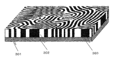
도 3은 핑거 프린트 패턴의 개요도.
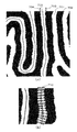
도 4는 핑거 프린트 패턴의 SEM 이미지와, 당해 SEM 이미지에 대해 패턴의 중심선을 추출한 윤곽선 화상의 일례를 나타내는 도면.
도 5는 추출된 중심선간의 거리를 측정하는 공정을 도시하는 도면.
도 6은 소정 영역 내의 중심선간의 거리값과 그 거리값을 나타내는 부위의 빈도와의 관계를 나타내는 히스토그램.
도 7은 핑거 프린트 패턴의 조도를 평가하는 예를 도시하는 도면.
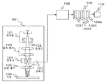
도 8은 주사 전자 현미경에 의해 얻어진 화상 정보를 사용하여, 패턴 계측을 실행하는 패턴 계측 장치의 개요를 도시하는 도면.
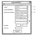
도 9는 측정 조건을 설정하기 위한 GUI(Graphical User Interface) 화면의 일례를 나타내는 도면.
101 : 전자총
102 : 전자선
103 : 집속 렌즈
104 : 편향기
105 : 대물 렌즈
106 : 시료
107 : 검출기
108 : 화상 처리부
109 : 연산부
110 : 출력부
Claims (17)
- 하전 입자선에 의해 취득된 화상에 기초하여 시료상의 패턴의 계측을 행하는 패턴 계측 장치에 있어서,
상기 시료상의 패턴의 직선 부분, 혹은 직선 근사할 수 있는 부분을 선택적으로 추출하고, 당해 추출 부분간의 거리의 측정, 당해 추출 부분의 소정 영역 내에 있어서의 비율, 및 당해 추출 부분의 길이 중 적어도 하나를 출력하는 연산 장치를 구비한 것을 특징으로 하는 패턴 계측 장치. - 제1항에 있어서,
상기 연산 장치는, 상기 시료상의 패턴의 중심이 되는 윤곽선간의 거리, 당해 윤곽선 내의 직선 부분의 비율, 및 직선 부분의 길이를 연산하는 것을 특징으로 하는 패턴 계측 장치. - 제1항에 있어서,
상기 시료상의 패턴은, 핑거 프린트 패턴인 것을 특징으로 하는 패턴 계측 장치. - 제3항에 있어서,
상기 연산 장치는, 상기 핑거 프린트 패턴의 하나의 패턴의 중심선과, 인접하는 패턴의 중심선 사이의 거리를 계측하는 것을 특징으로 하는 패턴 계측 장치. - 제3항에 있어서,
상기 연산 장치는, 상기 핑거 프린트 패턴의 중심선의 직선 부분을 추출하고, 당해 추출된 선분의 길이를 측정하는 것을 특징으로 하는 패턴 계측 장치. - 제3항에 있어서,
상기 연산 장치는, 상기 핑거 프린트 패턴의 소정 영역 내에 있어서의 직선 부분의 비율을 구하는 것을 특징으로 하는 패턴 계측 장치. - 제1항에 있어서,
상기 연산 장치는, 상기 패턴 중심선을 구성하는 점열의 직선 근사의 기울기와, 인접하는 점열의 근사 직선의 기울기를 비교하고, 기울기의 차에 의해 평행한지 여부를 판정하여, 평행 영역이 긴 부분을 직선으로 판정하는 것을 특징으로 하는 패턴 계측 장치. - 제1항에 있어서,
상기 연산 장치는, 상기 패턴 중심선을 구성하는 점열의 직선 근사의 기울기를, 중심선을 따라 연속적으로 산출하여, 기울기의 변화가 작은 부분을 직선으로 판정하는 것을 특징으로 하는 패턴 계측 장치. - 제1항에 있어서,
상기 연산 장치는, 상기 패턴 중심선을 구성하는 점열의 근사 곡선의 단위 길이당 곡률 반경을 구하여, 곡률 반경이 작은 부분을 직선으로 판정하는 것을 특징으로 하는 패턴 계측 장치. - 제1항에 있어서,
상기 연산 장치는, 상기 추출 부분간의 거리의 측정 결과마다의 빈도를 구하여, 특정 빈도의 측정 결과를, 상기 추출 부분간의 거리로서 출력하는 것을 특징으로 하는 패턴 계측 장치. - 제10항에 있어서,
상기 연산 장치는, 상기 빈도가 가장 큰 측정 결과를, 상기 추출 부분간의 거리로서 출력하는 것을 특징으로 하는 패턴 계측 장치. - 제1항에 있어서,
상기 시료상의 패턴은, 복수의 중합체를 포함하는 블록 공중합체의 마이크로 상 분리에 의해 형성되는 것인 것을 특징으로 하는 패턴 계측 장치. - 자기 조직화 리소그래피에 사용되는 고분자 화합물을 평가하는 평가 방법으로서, 하전 입자선 장치에 의해 얻어지는 핑거 프린트 패턴 화상 중으로부터, 패턴의 직선 부분, 혹은 직선 근사할 수 있는 부분을 선택적으로 추출하고, 당해 추출 부분간의 거리의 측정, 당해 추출 부분의 소정 영역 내에 있어서의 비율, 및 당해 추출 부분의 길이 중 적어도 하나를 구하는 것을 특징으로 하는 패턴의 평가 방법.
- 하전 입자선에 의해 취득된 화상에 기초하여 시료상의 패턴의 계측을 컴퓨터에 실행시키는 컴퓨터 프로그램에 있어서,
당해 프로그램은, 상기 컴퓨터에 상기 시료상의 패턴의 직선 부분, 혹은 직선 근사할 수 있는 부분을 선택적으로 추출시키고, 당해 추출 부분간의 거리의 측정, 당해 추출 부분의 소정 영역 내에 있어서의 비율, 및 당해 추출 부분의 길이 중 적어도 하나를 출력시키는 것을 특징으로 하는 컴퓨터 프로그램. - 시료에 대한 하전 입자선의 주사에 기초하여 얻어지는 신호를 사용하여, 지문 형상으로 랜덤한 방향성을 갖고 배열된 핑거 프린트 패턴을 측정하는 연산 장치를 구비한 패턴 계측 장치로서,
당해 연산 장치는, 상기 하전 입자선의 주사에 기초하여 얻어지는 신호로부터, 핑거 프린트 패턴의 중심선과, 좌우 양 에지를 추출하고, 중심선과 좌우 양 에지의 위치 관계에 기초하여, 상기 핑거 프린트 패턴의 특징량을 계산하는 것을 특징으로 하는 패턴 계측 장치. - 제15항에 있어서,
상기 핑거 프린트 패턴은, 2종의 중합체를 포함하는 블록 공중합체의 마이크로 상 분리에 의해 형성되는 것인 것을 특징으로 하는 패턴 계측 장치. - 제15항에 있어서,
상기 연산 장치는, 상기 패턴의 중심선과 좌우 에지의 거리의 편차를 구하는 것을 특징으로 하는 패턴 계측 장치.
Applications Claiming Priority (3)
| Application Number | Priority Date | Filing Date | Title |
|---|---|---|---|
| JP2012213385 | 2012-09-27 | ||
| JPJP-P-2012-213385 | 2012-09-27 | ||
| PCT/JP2013/070960 WO2014050305A1 (ja) | 2012-09-27 | 2013-08-02 | パターン計測装置、自己組織化リソグラフィに用いられる高分子化合物の評価方法、及びコンピュータープログラム |
Related Child Applications (1)
| Application Number | Title | Priority Date | Filing Date |
|---|---|---|---|
| KR1020177016777A Division KR101877696B1 (ko) | 2012-09-27 | 2013-08-02 | 패턴 계측 장치, 자기 조직화 리소그래피에 사용되는 고분자 화합물의 평가 방법 및 컴퓨터 프로그램 |
Publications (1)
| Publication Number | Publication Date |
|---|---|
| KR20150028362A true KR20150028362A (ko) | 2015-03-13 |
Family
ID=50387719
Family Applications (2)
| Application Number | Title | Priority Date | Filing Date |
|---|---|---|---|
| KR1020157004058A Ceased KR20150028362A (ko) | 2012-09-27 | 2013-08-02 | 패턴 계측 장치, 자기 조직화 리소그래피에 사용되는 고분자 화합물의 평가 방법 및 컴퓨터 프로그램 |
| KR1020177016777A Active KR101877696B1 (ko) | 2012-09-27 | 2013-08-02 | 패턴 계측 장치, 자기 조직화 리소그래피에 사용되는 고분자 화합물의 평가 방법 및 컴퓨터 프로그램 |
Family Applications After (1)
| Application Number | Title | Priority Date | Filing Date |
|---|---|---|---|
| KR1020177016777A Active KR101877696B1 (ko) | 2012-09-27 | 2013-08-02 | 패턴 계측 장치, 자기 조직화 리소그래피에 사용되는 고분자 화합물의 평가 방법 및 컴퓨터 프로그램 |
Country Status (5)
| Country | Link |
|---|---|
| US (1) | US9589343B2 (ko) |
| JP (2) | JP5891311B2 (ko) |
| KR (2) | KR20150028362A (ko) |
| TW (1) | TWI539544B (ko) |
| WO (1) | WO2014050305A1 (ko) |
Families Citing this family (5)
| Publication number | Priority date | Publication date | Assignee | Title |
|---|---|---|---|---|
| JP6088803B2 (ja) * | 2012-11-16 | 2017-03-01 | 株式会社日立ハイテクノロジーズ | 画像処理装置、自己組織化リソグラフィ技術によるパターン生成方法、及びコンピュータープログラム |
| CN106461464B (zh) * | 2014-05-13 | 2018-04-20 | 柯尼卡美能达株式会社 | 测色装置以及测色方法 |
| DE102015212618A1 (de) * | 2015-07-06 | 2017-01-12 | Fraunhofer-Gesellschaft zur Förderung der angewandten Forschung e.V. | Sicherheitsmerkmal, Verfahren zum Herstellen eines Sicherheitsmerkmals und Verfahren zum Authentifizieren eines Benutzers unter Verwendung eines Sicherheitsmerkmals |
| US10150323B2 (en) * | 2016-02-29 | 2018-12-11 | International Business Machines Corporation | Structure, system, method, and recording medium of implementing a directed self-assembled security pattern |
| US10812259B2 (en) | 2017-10-31 | 2020-10-20 | International Business Machines Corporation | Self-assembly based random number generator |
Family Cites Families (15)
| Publication number | Priority date | Publication date | Assignee | Title |
|---|---|---|---|---|
| JPH0674742A (ja) * | 1992-08-31 | 1994-03-18 | Mitsubishi Electric Corp | 電子ビーム寸法測定装置 |
| JP3412366B2 (ja) * | 1995-11-06 | 2003-06-03 | 日産自動車株式会社 | 塗膜平滑性検査装置 |
| JP4801427B2 (ja) * | 2005-01-04 | 2011-10-26 | 株式会社日立ハイテクノロジーズ | パターン形状評価方法 |
| JP2006269710A (ja) * | 2005-03-24 | 2006-10-05 | Toshiba Corp | パターン評価方法および半導体装置の製造方法 |
| JP4585926B2 (ja) | 2005-06-17 | 2010-11-24 | 株式会社日立ハイテクノロジーズ | パターンレイヤーデータ生成装置、それを用いたパターンレイヤーデータ生成システム、半導体パターン表示装置、パターンレイヤーデータ生成方法、及びコンピュータプログラム |
| JP2007081326A (ja) * | 2005-09-16 | 2007-03-29 | Dainippon Screen Mfg Co Ltd | 配線形成システムおよびその方法 |
| KR100663367B1 (ko) | 2005-12-06 | 2007-01-02 | 삼성전자주식회사 | 반도체소자의 시디 측정방법 및 관련된 측정기 |
| JP2007192594A (ja) * | 2006-01-17 | 2007-08-02 | Horon:Kk | パターン画像取得方法およびパターン画像取得装置 |
| EP1990212A1 (en) * | 2007-05-07 | 2008-11-12 | CSEM Centre Suisse d'Electronique et de Microtechnique SA Recherche et Développement | Unique security device for the identification or authentication of valuable goods, fabrication process and method for securing valuable goods using such a unique security device |
| JP5066252B2 (ja) * | 2008-03-10 | 2012-11-07 | 株式会社アドバンテスト | パターン測長装置及びパターン測長方法 |
| WO2010041731A1 (ja) * | 2008-10-10 | 2010-04-15 | 日本電気株式会社 | 照合装置、照合方法、及びプログラム |
| US8043964B2 (en) | 2009-05-20 | 2011-10-25 | Micron Technology, Inc. | Method for providing electrical connections to spaced conductive lines |
| US8114306B2 (en) | 2009-05-22 | 2012-02-14 | International Business Machines Corporation | Method of forming sub-lithographic features using directed self-assembly of polymers |
| JP5451577B2 (ja) * | 2010-11-05 | 2014-03-26 | 株式会社日立ハイテクノロジーズ | 同心円状パターンの検査装置および検査方法 |
| JP5542766B2 (ja) * | 2011-09-26 | 2014-07-09 | 株式会社東芝 | パターン形成方法 |
-
2013
- 2013-08-02 WO PCT/JP2013/070960 patent/WO2014050305A1/ja not_active Ceased
- 2013-08-02 KR KR1020157004058A patent/KR20150028362A/ko not_active Ceased
- 2013-08-02 US US14/422,603 patent/US9589343B2/en active Active
- 2013-08-02 KR KR1020177016777A patent/KR101877696B1/ko active Active
- 2013-08-02 JP JP2014538253A patent/JP5891311B2/ja active Active
- 2013-08-13 TW TW102128966A patent/TWI539544B/zh active
-
2016
- 2016-02-19 JP JP2016029462A patent/JP6349333B2/ja active Active
Also Published As
| Publication number | Publication date |
|---|---|
| WO2014050305A1 (ja) | 2014-04-03 |
| TWI539544B (zh) | 2016-06-21 |
| JP6349333B2 (ja) | 2018-06-27 |
| TW201430980A (zh) | 2014-08-01 |
| JPWO2014050305A1 (ja) | 2016-08-22 |
| KR20170073736A (ko) | 2017-06-28 |
| US9589343B2 (en) | 2017-03-07 |
| JP2016156817A (ja) | 2016-09-01 |
| KR101877696B1 (ko) | 2018-07-12 |
| JP5891311B2 (ja) | 2016-03-22 |
| US20150243008A1 (en) | 2015-08-27 |
Similar Documents
| Publication | Publication Date | Title |
|---|---|---|
| KR101727950B1 (ko) | 패턴 형상 평가 방법, 반도체 장치의 제조 방법 및 패턴 형상 평가 장치 | |
| JP5981838B2 (ja) | 検査画像内の欠陥を検出するためのシステム、方法及びコンピュータプログラム製品 | |
| JP5553716B2 (ja) | 欠陥検査方法及びその装置 | |
| JP3959355B2 (ja) | 微細パターンの3次元形状測定方法 | |
| US8538130B2 (en) | CD metrology system and method of classifying similar structural elements | |
| JP2013257304A5 (ko) | ||
| KR101877696B1 (ko) | 패턴 계측 장치, 자기 조직화 리소그래피에 사용되는 고분자 화합물의 평가 방법 및 컴퓨터 프로그램 | |
| US7439503B2 (en) | Charged particle beam irradiation method, method of manufacturing semiconductor device and charged particle beam apparatus | |
| CN1444035A (zh) | 检查图形的方法 | |
| US20130245989A1 (en) | Signal processing method and signal processing apparatus | |
| KR101810436B1 (ko) | 라인 패턴의 형상 평가 방법 및 그 장치 | |
| JP6147868B2 (ja) | パターン測定装置、及びコンピュータプログラム | |
| JP5478681B2 (ja) | 半導体欠陥検査装置ならびにその方法 | |
| JP5880134B2 (ja) | パターン計測方法およびパターン計測装置 | |
| TWI769662B (zh) | 帶電粒子線裝置及檢查裝置 | |
| US8884223B2 (en) | Methods and apparatus for measurement of relative critical dimensions | |
| KR101487113B1 (ko) | 패턴의 판정 장치 및 기록 매체 | |
| JP6266360B2 (ja) | 画像処理装置および荷電粒子線装置 | |
| JP2014093429A (ja) | 半導体検査装置および半導体検査方法 | |
| US20250027886A1 (en) | Defect inspection method and defect inspection system | |
| JP2004077422A (ja) | 試料像測長方法及び試料像測長装置 |
Legal Events
| Date | Code | Title | Description |
|---|---|---|---|
| A201 | Request for examination | ||
| PA0105 | International application |
Patent event date: 20150213 Patent event code: PA01051R01D Comment text: International Patent Application |
|
| PA0201 | Request for examination | ||
| PG1501 | Laying open of application | ||
| E902 | Notification of reason for refusal | ||
| PE0902 | Notice of grounds for rejection |
Comment text: Notification of reason for refusal Patent event date: 20160415 Patent event code: PE09021S01D |
|
| AMND | Amendment | ||
| E601 | Decision to refuse application | ||
| PE0601 | Decision on rejection of patent |
Patent event date: 20161129 Comment text: Decision to Refuse Application Patent event code: PE06012S01D Patent event date: 20160415 Comment text: Notification of reason for refusal Patent event code: PE06011S01I |
|
| X091 | Application refused [patent] | ||
| AMND | Amendment | ||
| PX0901 | Re-examination |
Patent event code: PX09011S01I Patent event date: 20161129 Comment text: Decision to Refuse Application Patent event code: PX09012R01I Patent event date: 20160811 Comment text: Amendment to Specification, etc. |
|
| PX0601 | Decision of rejection after re-examination |
Comment text: Decision to Refuse Application Patent event code: PX06014S01D Patent event date: 20170322 Comment text: Amendment to Specification, etc. Patent event code: PX06012R01I Patent event date: 20170228 Comment text: Decision to Refuse Application Patent event code: PX06011S01I Patent event date: 20161129 Comment text: Amendment to Specification, etc. Patent event code: PX06012R01I Patent event date: 20160811 Comment text: Notification of reason for refusal Patent event code: PX06013S01I Patent event date: 20160415 |
|
| X601 | Decision of rejection after re-examination | ||
| A107 | Divisional application of patent | ||
| PA0104 | Divisional application for international application |
Comment text: Divisional Application for International Patent Patent event code: PA01041R01D Patent event date: 20170619 |