KR20140133963A - Liquid crystal display device - Google Patents
Liquid crystal display device Download PDFInfo
- Publication number
- KR20140133963A KR20140133963A KR1020147030621A KR20147030621A KR20140133963A KR 20140133963 A KR20140133963 A KR 20140133963A KR 1020147030621 A KR1020147030621 A KR 1020147030621A KR 20147030621 A KR20147030621 A KR 20147030621A KR 20140133963 A KR20140133963 A KR 20140133963A
- Authority
- KR
- South Korea
- Prior art keywords
- common electrode
- sub
- pixel electrode
- main
- electrode
- Prior art date
Links
Images


Classifications
-
- G—PHYSICS
- G09—EDUCATION; CRYPTOGRAPHY; DISPLAY; ADVERTISING; SEALS
- G09G—ARRANGEMENTS OR CIRCUITS FOR CONTROL OF INDICATING DEVICES USING STATIC MEANS TO PRESENT VARIABLE INFORMATION
- G09G3/00—Control arrangements or circuits, of interest only in connection with visual indicators other than cathode-ray tubes
- G09G3/20—Control arrangements or circuits, of interest only in connection with visual indicators other than cathode-ray tubes for presentation of an assembly of a number of characters, e.g. a page, by composing the assembly by combination of individual elements arranged in a matrix no fixed position being assigned to or needed to be assigned to the individual characters or partial characters
- G09G3/34—Control arrangements or circuits, of interest only in connection with visual indicators other than cathode-ray tubes for presentation of an assembly of a number of characters, e.g. a page, by composing the assembly by combination of individual elements arranged in a matrix no fixed position being assigned to or needed to be assigned to the individual characters or partial characters by control of light from an independent source
- G09G3/36—Control arrangements or circuits, of interest only in connection with visual indicators other than cathode-ray tubes for presentation of an assembly of a number of characters, e.g. a page, by composing the assembly by combination of individual elements arranged in a matrix no fixed position being assigned to or needed to be assigned to the individual characters or partial characters by control of light from an independent source using liquid crystals
- G09G3/3611—Control of matrices with row and column drivers
-
- G—PHYSICS
- G02—OPTICS
- G02F—OPTICAL DEVICES OR ARRANGEMENTS FOR THE CONTROL OF LIGHT BY MODIFICATION OF THE OPTICAL PROPERTIES OF THE MEDIA OF THE ELEMENTS INVOLVED THEREIN; NON-LINEAR OPTICS; FREQUENCY-CHANGING OF LIGHT; OPTICAL LOGIC ELEMENTS; OPTICAL ANALOGUE/DIGITAL CONVERTERS
- G02F1/00—Devices or arrangements for the control of the intensity, colour, phase, polarisation or direction of light arriving from an independent light source, e.g. switching, gating or modulating; Non-linear optics
- G02F1/01—Devices or arrangements for the control of the intensity, colour, phase, polarisation or direction of light arriving from an independent light source, e.g. switching, gating or modulating; Non-linear optics for the control of the intensity, phase, polarisation or colour
- G02F1/13—Devices or arrangements for the control of the intensity, colour, phase, polarisation or direction of light arriving from an independent light source, e.g. switching, gating or modulating; Non-linear optics for the control of the intensity, phase, polarisation or colour based on liquid crystals, e.g. single liquid crystal display cells
- G02F1/133—Constructional arrangements; Operation of liquid crystal cells; Circuit arrangements
- G02F1/1333—Constructional arrangements; Manufacturing methods
- G02F1/1343—Electrodes
- G02F1/134309—Electrodes characterised by their geometrical arrangement
- G02F1/134363—Electrodes characterised by their geometrical arrangement for applying an electric field parallel to the substrate, i.e. in-plane switching [IPS]
-
- G—PHYSICS
- G02—OPTICS
- G02F—OPTICAL DEVICES OR ARRANGEMENTS FOR THE CONTROL OF LIGHT BY MODIFICATION OF THE OPTICAL PROPERTIES OF THE MEDIA OF THE ELEMENTS INVOLVED THEREIN; NON-LINEAR OPTICS; FREQUENCY-CHANGING OF LIGHT; OPTICAL LOGIC ELEMENTS; OPTICAL ANALOGUE/DIGITAL CONVERTERS
- G02F1/00—Devices or arrangements for the control of the intensity, colour, phase, polarisation or direction of light arriving from an independent light source, e.g. switching, gating or modulating; Non-linear optics
- G02F1/01—Devices or arrangements for the control of the intensity, colour, phase, polarisation or direction of light arriving from an independent light source, e.g. switching, gating or modulating; Non-linear optics for the control of the intensity, phase, polarisation or colour
- G02F1/13—Devices or arrangements for the control of the intensity, colour, phase, polarisation or direction of light arriving from an independent light source, e.g. switching, gating or modulating; Non-linear optics for the control of the intensity, phase, polarisation or colour based on liquid crystals, e.g. single liquid crystal display cells
- G02F1/133—Constructional arrangements; Operation of liquid crystal cells; Circuit arrangements
- G02F1/1333—Constructional arrangements; Manufacturing methods
- G02F1/1337—Surface-induced orientation of the liquid crystal molecules, e.g. by alignment layers
- G02F1/133707—Structures for producing distorted electric fields, e.g. bumps, protrusions, recesses, slits in pixel electrodes
-
- G—PHYSICS
- G02—OPTICS
- G02F—OPTICAL DEVICES OR ARRANGEMENTS FOR THE CONTROL OF LIGHT BY MODIFICATION OF THE OPTICAL PROPERTIES OF THE MEDIA OF THE ELEMENTS INVOLVED THEREIN; NON-LINEAR OPTICS; FREQUENCY-CHANGING OF LIGHT; OPTICAL LOGIC ELEMENTS; OPTICAL ANALOGUE/DIGITAL CONVERTERS
- G02F1/00—Devices or arrangements for the control of the intensity, colour, phase, polarisation or direction of light arriving from an independent light source, e.g. switching, gating or modulating; Non-linear optics
- G02F1/01—Devices or arrangements for the control of the intensity, colour, phase, polarisation or direction of light arriving from an independent light source, e.g. switching, gating or modulating; Non-linear optics for the control of the intensity, phase, polarisation or colour
- G02F1/13—Devices or arrangements for the control of the intensity, colour, phase, polarisation or direction of light arriving from an independent light source, e.g. switching, gating or modulating; Non-linear optics for the control of the intensity, phase, polarisation or colour based on liquid crystals, e.g. single liquid crystal display cells
- G02F1/133—Constructional arrangements; Operation of liquid crystal cells; Circuit arrangements
- G02F1/1333—Constructional arrangements; Manufacturing methods
- G02F1/1343—Electrodes
- G02F1/134309—Electrodes characterised by their geometrical arrangement
- G02F1/134336—Matrix
-
- G—PHYSICS
- G02—OPTICS
- G02F—OPTICAL DEVICES OR ARRANGEMENTS FOR THE CONTROL OF LIGHT BY MODIFICATION OF THE OPTICAL PROPERTIES OF THE MEDIA OF THE ELEMENTS INVOLVED THEREIN; NON-LINEAR OPTICS; FREQUENCY-CHANGING OF LIGHT; OPTICAL LOGIC ELEMENTS; OPTICAL ANALOGUE/DIGITAL CONVERTERS
- G02F1/00—Devices or arrangements for the control of the intensity, colour, phase, polarisation or direction of light arriving from an independent light source, e.g. switching, gating or modulating; Non-linear optics
- G02F1/01—Devices or arrangements for the control of the intensity, colour, phase, polarisation or direction of light arriving from an independent light source, e.g. switching, gating or modulating; Non-linear optics for the control of the intensity, phase, polarisation or colour
- G02F1/13—Devices or arrangements for the control of the intensity, colour, phase, polarisation or direction of light arriving from an independent light source, e.g. switching, gating or modulating; Non-linear optics for the control of the intensity, phase, polarisation or colour based on liquid crystals, e.g. single liquid crystal display cells
- G02F1/133—Constructional arrangements; Operation of liquid crystal cells; Circuit arrangements
- G02F1/136—Liquid crystal cells structurally associated with a semi-conducting layer or substrate, e.g. cells forming part of an integrated circuit
- G02F1/1362—Active matrix addressed cells
- G02F1/136213—Storage capacitors associated with the pixel electrode
-
- G—PHYSICS
- G02—OPTICS
- G02F—OPTICAL DEVICES OR ARRANGEMENTS FOR THE CONTROL OF LIGHT BY MODIFICATION OF THE OPTICAL PROPERTIES OF THE MEDIA OF THE ELEMENTS INVOLVED THEREIN; NON-LINEAR OPTICS; FREQUENCY-CHANGING OF LIGHT; OPTICAL LOGIC ELEMENTS; OPTICAL ANALOGUE/DIGITAL CONVERTERS
- G02F1/00—Devices or arrangements for the control of the intensity, colour, phase, polarisation or direction of light arriving from an independent light source, e.g. switching, gating or modulating; Non-linear optics
- G02F1/01—Devices or arrangements for the control of the intensity, colour, phase, polarisation or direction of light arriving from an independent light source, e.g. switching, gating or modulating; Non-linear optics for the control of the intensity, phase, polarisation or colour
- G02F1/13—Devices or arrangements for the control of the intensity, colour, phase, polarisation or direction of light arriving from an independent light source, e.g. switching, gating or modulating; Non-linear optics for the control of the intensity, phase, polarisation or colour based on liquid crystals, e.g. single liquid crystal display cells
- G02F1/133—Constructional arrangements; Operation of liquid crystal cells; Circuit arrangements
- G02F1/136—Liquid crystal cells structurally associated with a semi-conducting layer or substrate, e.g. cells forming part of an integrated circuit
- G02F1/1362—Active matrix addressed cells
- G02F1/1368—Active matrix addressed cells in which the switching element is a three-electrode device
-
- G—PHYSICS
- G02—OPTICS
- G02F—OPTICAL DEVICES OR ARRANGEMENTS FOR THE CONTROL OF LIGHT BY MODIFICATION OF THE OPTICAL PROPERTIES OF THE MEDIA OF THE ELEMENTS INVOLVED THEREIN; NON-LINEAR OPTICS; FREQUENCY-CHANGING OF LIGHT; OPTICAL LOGIC ELEMENTS; OPTICAL ANALOGUE/DIGITAL CONVERTERS
- G02F1/00—Devices or arrangements for the control of the intensity, colour, phase, polarisation or direction of light arriving from an independent light source, e.g. switching, gating or modulating; Non-linear optics
- G02F1/01—Devices or arrangements for the control of the intensity, colour, phase, polarisation or direction of light arriving from an independent light source, e.g. switching, gating or modulating; Non-linear optics for the control of the intensity, phase, polarisation or colour
- G02F1/13—Devices or arrangements for the control of the intensity, colour, phase, polarisation or direction of light arriving from an independent light source, e.g. switching, gating or modulating; Non-linear optics for the control of the intensity, phase, polarisation or colour based on liquid crystals, e.g. single liquid crystal display cells
- G02F1/133—Constructional arrangements; Operation of liquid crystal cells; Circuit arrangements
- G02F1/1333—Constructional arrangements; Manufacturing methods
- G02F1/1343—Electrodes
- G02F1/134309—Electrodes characterised by their geometrical arrangement
- G02F1/134318—Electrodes characterised by their geometrical arrangement having a patterned common electrode
Abstract
제1 방향을 따라 각각 연장된 게이트 배선 및 보조 용량선과, 제1 방향에 교차하는 제2 방향을 따라 각각 연장된 제1 소스 배선 및 제2 소스 배선과, 상기 제1 소스 배선과 상기 제2 소스 배선과의 사이에 위치하고 제2 방향을 따라 연장된 띠 형상의 주화소 전극과, 상기 주화소 전극에 연결되고 상기 제1 소스 배선 및 상기 제2 소스 배선을 향해 제1 방향을 따라 각각 연장된 띠 형상의 부화소 전극과, 수평 배향성을 나타내는 재료에 의해 형성되고 상기 주화소 전극 및 상기 부화소 전극을 덮는 제1 배향막을 구비한 제1 기판과, 상기 주화소 전극을 사이에 둔 양측에서 제2 방향을 따라 각각 연장된 제2 주공통 전극과, 상기 제2 주공통 전극에 연결되고 상기 부화소 전극을 사이에 둔 양측에서 제1 방향을 따라 각각 연장된 제2 부공통 전극과, 수평 배향성을 나타내는 재료에 의해 형성되고 상기 제2 주공통 전극 및 상기 제2 부공통 전극을 덮는 제2 배향막을 구비한 제2 기판과, 상기 제1 기판과 상기 제2 기판과의 사이에 보유 지지된 액정 분자를 포함하는 액정층을 구비한 것을 특징으로 하는 액정 표시 장치.A first source wiring and a second source wiring respectively extending along a second direction crossing the first direction and a gate wiring and an auxiliary capacitance line respectively extending along the first direction, A strip-shaped main pixel electrode positioned between the first pixel electrode and the second pixel electrode and extending along the second direction, and a strip connected to the main pixel electrode and extending along the first direction toward the first source wiring and the second source wiring, And a first alignment film formed by a material exhibiting a horizontal alignment property and covering the main pixel electrode and the sub pixel electrode, and a second alignment film covering the main pixel electrode and the sub pixel electrode, A second sub-common electrode connected to the second main common electrode and extending along the first direction at both sides with the sub-pixel electrode therebetween, and a second sub-common electrode extending from the first sub- I And a second alignment film formed on the first main electrode and covering the second main common electrode and the second sub common electrode, and a second alignment film formed between the liquid crystal molecules And a liquid crystal layer including the liquid crystal layer.
Description
본 발명의 실시 형태는, 액정 표시 장치에 관한 것이다.An embodiment of the present invention relates to a liquid crystal display device.
최근, 평면 표시 장치가 활발히 개발되고 있고, 그 중에서도 액정 표시 장치는, 경량, 박형, 저소비 전력 등의 이점으로부터 특히 주목을 모으고 있다. 특히, 각 화소에 스위칭 소자를 포함한 액티브 매트릭스형 액정 표시 장치에 있어서는, IPS(In―Plane Switching) 모드나 FFS(Fringe Field Switching) 모드 등의 횡전계(프린지 전계도 포함함)를 이용한 구조가 주목받고 있다. 이러한 횡전계 모드의 액정 표시 장치는, 어레이 기판에 형성된 화소 전극과 대향 전극을 구비하고, 어레이 기판의 주면에 대하여 거의 평행한 횡전계로 액정 분자를 스위칭한다.2. Description of the Related Art In recent years, flat display devices have been actively developed, and in particular, liquid crystal display devices have attracted particular attention due to advantages such as light weight, thinness, and low power consumption. Particularly, in an active matrix liquid crystal display device including a switching element in each pixel, a structure using a transverse electric field (including a fringing electric field) such as an IPS (In-Plane Switching) mode or an FFS (Fringe Field Switching) . Such a transverse electric field mode liquid crystal display device has pixel electrodes and counter electrodes formed on an array substrate and switches liquid crystal molecules in a transverse electric field substantially parallel to the main surface of the array substrate.
한편, 어레이 기판에 형성된 화소 전극과, 대향 기판에 형성된 대향 전극과의 사이에, 횡전계 혹은 경사 전계를 형성하고, 액정 분자를 스위칭하는 기술도 제안되어 있다.On the other hand, a technique of switching a liquid crystal molecule by forming a transverse electric field or an oblique electric field between the pixel electrode formed on the array substrate and the counter electrode formed on the counter substrate has been proposed.
본 실시 형태의 목적은, 표시 품위가 양호한 액정 표시 장치를 제공하는 것에 있다.An object of the present embodiment is to provide a liquid crystal display device having a good display quality.
본 실시 형태에 따르면,According to the present embodiment,
제1 방향을 따라 각각 연장된 게이트 배선 및 보조 용량선과, 제1 방향에 교차하는 제2 방향을 따라 각각 연장된 제1 소스 배선 및 제2 소스 배선과, 상기 제1 소스 배선과 상기 제2 소스 배선과의 사이에 위치하고 제2 방향을 따라 연장된 띠 형상의 주화소 전극과, 상기 주화소 전극에 연결되고 상기 제1 소스 배선 및 상기 제2 소스 배선을 향해 제1 방향을 따라 각각 연장된 띠 형상의 부화소 전극과, 수평 배향성을 나타내는 재료에 의해 형성되고 상기 주화소 전극 및 상기 부화소 전극을 덮는 제1 배향막을 구비한 제1 기판과, 상기 주화소 전극을 사이에 둔 양측에서 제2 방향을 따라 각각 연장된 제2 주공통 전극과, 상기 제2 주공통 전극에 연결되고 상기 부화소 전극을 사이에 둔 양측에서 제1 방향을 따라 각각 연장된 제2 부공통 전극과, 수평 배향성을 나타내는 재료에 의해 형성되고 상기 제2 주공통 전극 및 상기 제2 부공통 전극을 덮는 제2 배향막을 구비한 제2 기판과, 상기 제1 기판과 상기 제2 기판과의 사이에 보유 지지된 액정 분자를 포함하는 액정층을 구비한 것을 특징으로 하는 액정 표시 장치가 제공된다.A first source wiring and a second source wiring respectively extending along a second direction crossing the first direction and a gate wiring and an auxiliary capacitance line respectively extending along the first direction, A strip-shaped main pixel electrode positioned between the first pixel electrode and the second pixel electrode and extending along the second direction, and a strip connected to the main pixel electrode and extending along the first direction toward the first source wiring and the second source wiring, And a first alignment film formed by a material exhibiting a horizontal alignment property and covering the main pixel electrode and the sub pixel electrode, and a second alignment film covering the main pixel electrode and the sub pixel electrode, A second sub-common electrode connected to the second main common electrode and extending along the first direction at both sides with the sub-pixel electrode therebetween, and a second sub-common electrode extending from the first sub- I And a second alignment film formed on the first main electrode and covering the second main common electrode and the second sub common electrode, and a second alignment film formed between the liquid crystal molecules And a liquid crystal layer including the liquid crystal layer.
본 실시 형태에 따르면,According to the present embodiment,
제1 방향을 따라 각각 연장된 게이트 배선 및 보조 용량선과, 제1 방향에 교차하는 제2 방향을 따라 각각 연장된 제1 소스 배선 및 제2 소스 배선과, 상기 제1 소스 배선과 상기 제2 소스 배선과의 사이에 위치하고 제2 방향을 따라 연장된 띠 형상의 주화소 전극과, 상기 주화소 전극에 연결되고 상기 제1 소스 배선 및 상기 제2 소스 배선을 향해 제1 방향을 따라 각각 연장된 띠 형상의 부화소 전극과, 상기 제1 소스 배선 및 상기 제2 소스 배선과 각각 대향하고 제2 방향을 따라 연장된 제1 주공통 전극과, 수평 배향성을 나타내는 재료에 의해 형성되고 상기 주화소 전극, 상기 부화소 전극 및 상기 제1 주공통 전극을 덮는 제1 배향막을 구비한 제1 기판과, 상기 부화소 전극을 사이에 둔 양측에서 제1 방향을 따라 각각 연장되고 상기 제1 주공통 전극과 동일 전위의 제2 부공통 전극과, 수평 배향성을 나타내는 재료에 의해 형성되고 상기 제2 부공통 전극을 덮는 제2 배향막을 구비한 제2 기판과, 상기 제1 기판과 상기 제2 기판과의 사이에 보유 지지된 액정 분자를 포함하는 액정층을 구비한 것을 특징으로 하는 액정 표시 장치가 제공된다.A first source wiring and a second source wiring respectively extending along a second direction crossing the first direction and a gate wiring and an auxiliary capacitance line respectively extending along the first direction, A strip-shaped main pixel electrode positioned between the first pixel electrode and the second pixel electrode and extending along the second direction, and a strip connected to the main pixel electrode and extending along the first direction toward the first source wiring and the second source wiring, A first main common electrode opposing each of the first source wiring and the second source wiring and extending along a second direction; and a second main common electrode formed by a material exhibiting horizontal orientation, Pixel electrode and a first main electrode common to the first main common electrode, and a second substrate having a first main electrode formed on the first main electrode and extending along a first direction on both sides of the sub- I'm And a second alignment film formed by a material exhibiting horizontal orientation and covering the second sub common electrode, and a second alignment film formed between the first substrate and the second substrate There is provided a liquid crystal display device comprising a liquid crystal layer containing supported liquid crystal molecules.
본 실시 형태에 따르면,According to the present embodiment,
제1 방향을 따라 각각 연장된 게이트 배선 및 보조 용량선과, 제1 방향에 교차하는 제2 방향을 따라 각각 연장된 제1 소스 배선 및 제2 소스 배선과, 상기 제1 소스 배선과 상기 제2 소스 배선과의 사이에 위치하고 제2 방향을 따라 연장된 띠 형상의 주화소 전극과, 상기 주화소 전극에 연결되고 상기 제1 소스 배선 및 상기 제2 소스 배선을 향해 제1 방향을 따라 각각 연장된 띠 형상의 부화소 전극과, 상기 게이트 배선과 대향하고 제1 방향을 따라 연장된 제1 부공통 전극과, 수평 배향성을 나타내는 재료에 의해 형성되고 상기 주화소 전극, 상기 부화소 전극 및 상기 제1 부공통 전극을 덮는 제1 배향막을 구비한 제1 기판과, 상기 주화소 전극을 사이에 둔 양측에서 제2 방향을 따라 각각 연장되고 상기 제1 부공통 전극과 동일 전위의 제2 주공통 전극과, 수평 배향성을 나타내는 재료에 의해 형성되고 상기 제2 주공통 전극을 덮는 제2 배향막을 구비한 제2 기판과, 상기 제1 기판과 상기 제2 기판과의 사이에 보유 지지된 액정 분자를 포함하는 액정층을 구비한 것을 특징으로 하는 액정 표시 장치가 제공된다.A first source wiring and a second source wiring respectively extending along a second direction crossing the first direction and a gate wiring and an auxiliary capacitance line respectively extending along the first direction, A strip-shaped main pixel electrode positioned between the first pixel electrode and the second pixel electrode and extending along the second direction, and a strip connected to the main pixel electrode and extending along the first direction toward the first source wiring and the second source wiring, Pixel electrode, a first sub-common electrode opposed to the gate wiring and extending along a first direction, and a second sub-common electrode formed of a material exhibiting horizontal orientation, the main sub-pixel electrode, the sub- A second main common electrode extending along a second direction on both sides of the main pixel electrode and having the same potential as that of the first sub common electrode; Horizontal A liquid crystal layer including liquid crystal molecules held between the first substrate and the second substrate, and a second alignment film formed of a material exhibiting alignment properties and covering the second main common electrode; And a liquid crystal display device.
도 1은 본 실시 형태에 있어서의 액정 표시 장치의 구성을 개략적으로 도시하는 도면이다.
도 2는 도 1에 도시한 액정 표시 패널의 구성 및 등가 회로를 개략적으로 도시하는 도면이다.
도 3은 본 실시 형태의 기본 구성에 대해 1화소에 있어서의 최소의 단위 구성체를 개략적으로 도시하는 평면도이다.
도 4는 스위칭 소자를 포함하는 액정 표시 패널의 단면을 개략적으로 도시하는 단면도이다.
도 5는 본 실시 형태의 제1 구성예에 있어서의 액정 표시 패널의 대향 기판에 있어서의 1화소의 구조를 개략적으로 도시하는 평면도이다.
도 6은 본 실시 형태의 제1 구성예에 있어서의 액정 표시 패널의 1화소를 대향 기판측에서 보았을 때의 어레이 기판의 구조를 개략적으로 도시하는 평면도이다.
도 7은 본 실시 형태의 제2 구성예에 있어서의 액정 표시 패널의 대향 기판에 있어서의 1화소의 구조를 개략적으로 도시하는 평면도이다.
도 8은 본 실시 형태의 제2 구성예에 있어서의 액정 표시 패널의 1화소를 대향 기판측에서 보았을 때의 어레이 기판의 구조를 개략적으로 도시하는 평면도이다.
도 9는 본 실시 형태의 제3 구성예에 있어서의 액정 표시 패널의 대향 기판에 있어서의 1화소의 구조를 개략적으로 도시하는 평면도이다.
도 10은 본 실시 형태의 제3 구성예에 있어서의 액정 표시 패널의 1화소를 대향 기판측에서 보았을 때의 어레이 기판의 구조를 개략적으로 도시하는 평면도이다.
도 11은 본 실시 형태의 제4 구성예에 있어서의 액정 표시 패널의 1화소를 대향 기판측에서 보았을 때의 어레이 기판의 구조를 개략적으로 도시하는 평면도이다.
도 12는 제1 내지 제4 구성예에서 설명한 어레이 기판과, 제1 내지 제3 구성예에서 설명한 대향 기판과의 조합을 정리한 도면이다.
도 13은 본 실시 형태의 배리에이션의 하나를 개략적으로 도시하는 평면도이다.Fig. 1 is a view schematically showing a configuration of a liquid crystal display device according to the present embodiment.
Fig. 2 is a view schematically showing the configuration and equivalent circuit of the liquid crystal display panel shown in Fig.
3 is a plan view schematically showing a minimum unit structure in one pixel with respect to the basic structure of the present embodiment.
4 is a cross-sectional view schematically showing a cross section of a liquid crystal display panel including a switching element.
5 is a plan view schematically showing the structure of one pixel in the counter substrate of the liquid crystal display panel in the first configuration example of the present embodiment.
6 is a plan view schematically showing the structure of an array substrate when one pixel of the liquid crystal display panel in the first configuration example of the present embodiment is viewed from the side of the counter substrate.
Fig. 7 is a plan view schematically showing the structure of one pixel in the counter substrate of the liquid crystal display panel in the second configuration example of the present embodiment. Fig.
8 is a plan view schematically showing the structure of the array substrate when one pixel of the liquid crystal display panel in the second configuration example of the present embodiment is viewed from the side of the counter substrate.
Fig. 9 is a plan view schematically showing the structure of one pixel in the counter substrate of the liquid crystal display panel in the third configuration example of the present embodiment. Fig.
10 is a plan view schematically showing the structure of an array substrate when one pixel of the liquid crystal display panel in the third configuration example of the present embodiment is viewed from the side of the counter substrate.
11 is a plan view schematically showing the structure of an array substrate when one pixel of the liquid crystal display panel in the fourth example of the present embodiment is viewed from the side of the counter substrate.
12 is a diagram summarizing combinations of the array substrate described in the first to fourth structural examples and the counter substrate described in the first to third structural examples.
13 is a plan view schematically showing one variation of this embodiment.
이하, 본 실시 형태에 대해, 도면을 참조하면서 상세하게 설명한다. 또한, 각 도면에 있어서, 동일 또는 유사한 기능을 발휘하는 구성 요소에는 동일한 참조 부호를 부여하고, 중복되는 설명은 생략한다.Hereinafter, this embodiment will be described in detail with reference to the drawings. In the drawings, the same reference numerals denote the same or similar components, and a duplicate description thereof is omitted.
도 1은 본 실시 형태에 있어서의 액정 표시 장치(1)의 구성을 개략적으로 도시하는 도면이다.Fig. 1 is a view schematically showing the configuration of a liquid
즉, 액정 표시 장치(1)는, 액티브 매트릭스 타입의 액정 표시 패널(LPN), 액정 표시 패널(LPN)에 접속된 구동 IC 칩(2) 및 플렉시블 배선 기판(3), 액정 표시 패널(LPN)을 조명하는 백라이트(4) 등을 구비하고 있다.That is, the liquid
액정 표시 패널(LPN)은, 제1 기판인 어레이 기판(AR)과, 어레이 기판(AR)에 대향하여 배치된 제2 기판인 대향 기판(CT)과, 이들 어레이 기판(AR)과 대향 기판(CT)과의 사이에 보유 지지된 도시하지 않은 액정층을 구비하여 구성되어 있다. 이러한 액정 표시 패널(LPN)은, 화상을 표시하는 액티브 에어리어(ACT)를 구비하고 있다. 이 액티브 에어리어(ACT)는, m×n개의 매트릭스 형상으로 배치된 복수의 화소(PX)에 의해 구성되어 있다(단, m 및 n은 양의 정수임).The liquid crystal display panel LPN includes an array substrate AR as a first substrate, an opposing substrate CT as a second substrate opposed to the array substrate AR, And a liquid crystal layer (not shown) held between the liquid crystal layer (not shown) and the liquid crystal layer (not shown). Such a liquid crystal display panel (LPN) has an active area (ACT) for displaying an image. The active area ACT is constituted by a plurality of pixels PX arranged in an m x n matrix (where m and n are positive integers).
백라이트(4)는, 도시한 예에서는, 어레이 기판(AR)의 배면측에 배치되어 있다. 이러한 백라이트(4)로서는, 다양한 형태가 적용 가능하고, 또한, 광원으로서 발광 다이오드(LED)를 이용한 것이나 냉음극관(CCFL)을 이용한 것 등 어느 것이나 적용 가능하며, 상세한 구조에 대해서는 설명을 생략한다.The
도 2는 도 1에 도시한 액정 표시 패널(LPN)의 구성 및 등가 회로를 개략적으로 도시하는 도면이다.Fig. 2 is a view schematically showing the configuration and equivalent circuit of the liquid crystal display panel (LPN) shown in Fig.
액정 표시 패널(LPN)은, 액티브 에어리어(ACT)에 있어서, n개의 게이트 배선(G)(G1∼Gn), n개의 보조 용량선(C)(C1∼Cn), m개의 소스 배선(S)(S1∼Sm) 등을 구비하고 있다. 게이트 배선(G) 및 보조 용량선(C)은, 예를 들어, 제1 방향(X)을 따라 대략 직선적으로 연장되어 있다. 이들 게이트 배선(G) 및 보조 용량선(C)은, 제1 방향(X)에 교차하는 제2 방향(Y)을 따라 간격을 두고 인접하고, 교대로 병렬 배치되어 있다. 여기에서는, 제1 방향(X)과 제2 방향(Y)은 서로 직교하고 있다. 소스 배선(S)은, 게이트 배선(G) 및 보조 용량선(C)과 교차하고 있다. 소스 배선(S)은, 제2 방향(Y)을 따라 대략 직선적으로 연장되어 있다. 또한, 게이트 배선(G), 보조 용량선(C) 및 소스 배선(S)은, 반드시 직선적으로 연장되어 있지 않아도 되고, 그들의 일부가 굴곡되어 있어도 된다.The liquid crystal display panel LPN includes n gate wirings G1 to Gn, n storage capacitor lines C to Cn, m source wirings S in the active area ACT, (S1 to Sm) and the like. The gate line G and the storage capacitor line C extend substantially linearly along the first direction X, for example. The gate lines G and the storage capacitor lines C are arranged adjacent to each other at intervals along a second direction Y intersecting the first direction X and are alternately arranged in parallel. Here, the first direction X and the second direction Y are orthogonal to each other. The source wiring S intersects the gate wiring G and the storage capacitor line C. [ The source wiring S extends substantially linearly along the second direction Y. The gate wiring G, the storage capacitor line C, and the source wiring S may not necessarily be linearly extended, and some of them may be bent.
각 게이트 배선(G)은, 액티브 에어리어(ACT)의 외측으로 인출되고, 게이트 드라이버(GD)에 접속되어 있다. 각 소스 배선(S)은, 액티브 에어리어(ACT)의 외측으로 인출되고, 소스 드라이버(SD)에 접속되어 있다. 이들 게이트 드라이버(GD) 및 소스 드라이버(SD)의 적어도 일부는, 예를 들어, 어레이 기판(AR)에 형성되고, 컨트롤러를 내장한 구동 IC 칩(2)과 접속되어 있다.Each gate wiring G is drawn out of the active area ACT and connected to the gate driver GD. Each source wiring S is drawn out of the active area ACT and connected to the source driver SD. At least a part of the gate driver GD and the source driver SD is formed on, for example, the array substrate AR and connected to the
각 화소(PX)는, 스위칭 소자(SW), 화소 전극(PE), 공통 전극(CE) 등을 구비하고 있다. 유지 용량(Cs)은, 예를 들어 보조 용량선(C)과 화소 전극(PE)과의 사이에 형성된다. 보조 용량선(C)은, 보조 용량 전압이 인가되는 전압 인가부(VCS)와 전기적으로 접속되어 있다.Each pixel PX includes a switching element SW, a pixel electrode PE, a common electrode CE, and the like. The storage capacitor Cs is formed, for example, between the storage capacitor line C and the pixel electrode PE. The storage capacitor line C is electrically connected to the voltage applying portion VCS to which the storage capacitor voltage is applied.
또한, 본 실시 형태에 있어서는, 액정 표시 패널(LPN)은, 화소 전극(PE)이 어레이 기판(AR)에 형성되는 한편, 공통 전극(CE)의 적어도 일부가 대향 기판(CT)에 형성된 구성이며, 이들 화소 전극(PE)과 공통 전극(CE)과의 사이에 형성되는 전계를 주로 이용하여 액정층(LQ)의 액정 분자를 스위칭한다. 화소 전극(PE)과 공통 전극(CE)과의 사이에 형성되는 전계는, 제1 방향(X)과 제2 방향(Y)에 의해 규정되는 X―Y 평면 혹은 어레이 기판(AR)의 기판 주면 혹은 대향 기판(CT)의 기판 주면에 대하여 약간 기운 경사 전계(혹은, 기판 주면에 거의 평행한 횡전계)이다.In the present embodiment, the liquid crystal display panel LPN is configured such that the pixel electrodes PE are formed on the array substrate AR, while at least a part of the common electrodes CE is formed on the counter substrate CT , And the liquid crystal molecules of the liquid crystal layer (LQ) are switched by mainly using an electric field formed between the pixel electrode (PE) and the common electrode (CE). The electric field formed between the pixel electrode PE and the common electrode CE is formed in the X-Y plane defined by the first direction X and the second direction Y, Or a slightly inclined electric field (or a transverse electric field substantially parallel to the main surface of the substrate) with respect to the main surface of the substrate of the counter substrate (CT).
스위칭 소자(SW)는, 예를 들어, n 채널 박막 트랜지스터(TFT)에 의해 구성되어 있다. 이 스위칭 소자(SW)는, 게이트 배선(G) 및 소스 배선(S)과 전기적으로 접속되어 있다. 액티브 에어리어(ACT)에는, m×n개의 스위칭 소자(SW)가 형성되어 있다.The switching element SW is constituted by, for example, an n-channel thin film transistor (TFT). The switching element SW is electrically connected to the gate wiring G and the source wiring S. In the active area ACT, m x n switching elements SW are formed.
화소 전극(PE)은, 각 화소(PX)에 배치되고, 스위칭 소자(SW)에 전기적으로 접속되어 있다. 액티브 에어리어(ACT)에는, m×n개의 화소 전극(PE)이 형성되어 있다. 공통 전극(CE)은, 예를 들어 공통 전위이며, 액정층(LQ)을 통해 복수의 화소(PX)의 화소 전극(PE)에 대하여 공통으로 배치되어 있다.The pixel electrode PE is disposed in each pixel PX and is electrically connected to the switching element SW. In the active area ACT, m x n number of pixel electrodes PE are formed. The common electrodes CE are, for example, a common potential and are arranged in common to the pixel electrodes PE of the plurality of pixels PX through the liquid crystal layer LQ.
어레이 기판(AR)은, 공통 전극(CE)에 전압을 인가하기 위한 급전부(VS)를 구비하고 있다. 이 급전부(VS)는, 예를 들어, 액티브 에어리어(ACT)의 외측에 형성되어 있다. 공통 전극(CE) 중, 대향 기판(CT)에 형성된 공통 전극(CE)의 적어도 일부는, 액티브 에어리어(ACT)의 외측으로 인출되고, 도시하지 않은 도전 부재를 통해, 어레이 기판(AR)에 형성된 급전부(VS)와 전기적으로 접속되어 있다. 또한, 공통 전극(CE)의 일부가 어레이 기판(AR)에 형성된 경우에는, 어레이 기판(AR)에 형성된 공통 전극(CE)의 일부는 예를 들어 액티브 에어리어(ACT)의 외측에서 급전부(VS)와 전기적으로 접속되어 있다.The array substrate AR has a power supply portion VS for applying a voltage to the common electrode CE. This feeding portion VS is formed, for example, on the outside of the active area ACT. At least a part of the common electrode CE formed on the counter substrate CT out of the common electrode CE is drawn out of the active area ACT and is formed on the array substrate AR through a conductive member And is electrically connected to the power feeding section VS. When a part of the common electrode CE is formed on the array substrate AR, a part of the common electrode CE formed on the array substrate AR is electrically connected to the power feeding part VS As shown in Fig.
이하에, 본 실시 형태의 기본 구성에 대해 설명한다.Hereinafter, the basic configuration of the present embodiment will be described.
도 3은 1화소(PX)에 있어서의 최소의 단위 구성체를 개략적으로 도시하는 평면도이다.3 is a plan view schematically showing a minimum unit structure in one pixel PX.
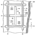
화소 전극(PE)은, 주화소 전극(PA) 및 부화소 전극(PB)을 갖고 있다. 이들 주화소 전극(PA) 및 부화소 전극(PB)은, 서로 전기적으로 접속되어 있다. 본 실시 형태에 있어서는, 주화소 전극(PA) 및 부화소 전극(PB)이 모두 어레이 기판(AR)에 구비되어 있다. 주화소 전극(PA)은, 제2 방향(Y)을 따라 연장되어 있다. 부화소 전극(PB)은, 제2 방향(Y)과는 다른 제1 방향(X)을 따라 연장되어 있다.The pixel electrode PE has a main pixel electrode PA and a sub-pixel electrode PB. The main pixel electrode PA and the sub-pixel electrode PB are electrically connected to each other. In the present embodiment, the main pixel electrode PA and the sub-pixel electrode PB are all provided on the array substrate AR. The main pixel electrode PA extends along the second direction Y. [ The sub pixel electrode PB extends along the first direction X different from the second direction Y. [
도시한 예에서는, 화소 전극(PE)은, 대략 십자 형상으로 형성되어 있다. 보다 구체적으로는, 주화소 전극(PA)은, 대략 화소 중앙부에 있어서 제2 방향(Y)을 따라 직선적으로 연장된 띠 형상으로 형성되어 있다. 부화소 전극(PB)은, 화소 중앙부에 있어서 제1 방향(X)을 따라 직선적으로 연장된 띠 형상으로 형성되어 있다.In the illustrated example, the pixel electrode PE is formed in a substantially cross shape. More specifically, the main pixel electrode PA is formed in a strip shape linearly extending along the second direction Y substantially at the center of the pixel. The sub-pixel electrode PB is formed in a strip shape linearly extending along the first direction X at the central portion of the pixel.
부화소 전극(PB)은, 주화소 전극(PA)의 대략 중앙부[혹은 주화소 전극(PA)의 제2 방향(Y)을 따른 길이의 중간점 부근]에 결합하고, 주화소 전극(PA)으로부터 그 양측, 즉 화소(PX)의 좌측 및 우측을 향해 연장되어 있다. 환언하면, 주화소 전극(PA)은, 부화소 전극(PB)의 대략 중앙부[혹은 부화소 전극(PB)의 제1 방향(X)을 따른 길이의 중간점 부근]에 결합하고, 부화소 전극(PB)으로부터 그 양측, 즉 화소(PX)의 상측 및 하측을 향해 연장되어 있다. 이들 주화소 전극(PA) 및 부화소 전극(PB)은, 서로 대략 직교하고 있다. 화소 전극(PE)은, 예를 들어, 부화소 전극(PB)에 있어서 도시를 생략한 스위칭 소자와 전기적으로 접속되어 있다.The sub pixel electrode PB is connected to the substantially central portion of the main pixel electrode PA (or the vicinity of the middle point of the length along the second direction Y of the main pixel electrode PA) That is, the left and right sides of the pixel PX. In other words, the main pixel electrode PA is coupled to the substantially central portion of the sub-pixel electrode PB (or near the midpoint of the length along the first direction X of the sub-pixel electrode PB) Extends from the pixel electrode PB toward both sides thereof, that is, the upper side and the lower side of the pixel PX. The main pixel electrode PA and the sub-pixel electrode PB are substantially orthogonal to each other. The pixel electrode PE is electrically connected to, for example, a switching element (not shown) in the sub-pixel electrode PB.
공통 전극(CE)은, 주공통 전극(CA) 및 부공통 전극(CB)을 갖고 있다. 이들 주공통 전극(CA) 및 부공통 전극(CB)은, 서로 전기적으로 접속되어 있다. 이러한 공통 전극(CE)은, 화소 전극(PE)과는 전기적으로 절연되어 있다. 본 실시 형태에 있어서는, 공통 전극(CE)에 있어서, 주공통 전극(CA) 및 부공통 전극(CB)의 적어도 일부는, 대향 기판(CT)에 구비되어 있다.The common electrode CE has a main common electrode CA and a sub common electrode CB. The main common electrode CA and the sub common electrode CB are electrically connected to each other. The common electrode CE is electrically insulated from the pixel electrode PE. In the present embodiment, at least a part of the main common electrode CA and the sub common electrode CB in the common electrode CE is provided in the counter substrate CT.
주공통 전극(CA)은, 제2 방향(Y)을 따라 연장되어 있다. 이 주공통 전극(CA)은, 주화소 전극(PA)을 사이에 둔 양측에 배치되어 있다. 이때, X―Y 평면 내에 있어서, 주공통 전극(CA)의 어느 것이나 주화소 전극(PA)과는 겹치지 않고, 주공통 전극(CA)의 각각과 주화소 전극(PA)과의 사이에는 대략 동등한 간격이 형성되어 있다. 즉, 주화소 전극(PA)은, 인접하는 주공통 전극(CA)의 대략 중간에 위치하고 있다.The main common electrode (CA) extends along the second direction (Y). The main common electrode CA is disposed on both sides of the main pixel electrode PA. At this time, in the X-Y plane, none of the main common electrodes CA overlap with the main pixel electrodes PA, and substantially equal to each other between the main common electrodes CA and the main pixel electrodes PA A gap is formed. That is, the main pixel electrode PA is located approximately in the middle of the adjacent main common electrode CA.
부공통 전극(CB)은, 제1 방향(X)을 따라 연장되어 있다. 부공통 전극(CB)은, 부화소 전극(PB)을 사이에 둔 양측에 배치되어 있다. 이때, X―Y 평면 내에 있어서, 부공통 전극(CB)의 어느 것이나 부화소 전극(PB)과는 겹치지 않고, 부공통 전극(CB)의 각각과 부화소 전극(PB)과의 사이에는 대략 동등한 간격이 형성되어 있다. 즉, 부화소 전극(PB)은, 인접하는 부공통 전극(CB)의 대략 중간에 위치하고 있다.The auxiliary common electrode CB extends in the first direction X. The auxiliary common electrode CB is disposed on both sides of the sub-pixel electrode PB. At this time, in the X-Y plane, none of the sub-common electrodes CB overlap with the sub-pixel electrodes PB, and each of the sub-common electrodes CB and the sub- A gap is formed. That is, the sub-pixel electrode PB is located approximately in the middle of the adjacent sub-common electrode CB.
도시한 예에서는, 주공통 전극(CA)은, 제2 방향(Y)을 따라 직선적으로 연장된 띠 형상으로 형성되어 있다. 부공통 전극(CB)은, 제1 방향(X)을 따라 직선적으로 연장된 띠 형상으로 형성되어 있다. 또한, 주공통 전극(CA)은 제1 방향(X)을 따라 간격을 두고 2개 평행하게 배열되어 있고, 이하에서는, 이들을 구별하기 위해, 도면 중의 좌측의 주공통 전극을 CAL이라고 칭하고, 도면 중의 우측의 주공통 전극을 CAR이라고 칭한다. 또한, 부공통 전극(CB)은 제2 방향(Y)을 따라 간격을 두고 2개 평행하게 배열되어 있고, 이하에서는, 이들을 구별하기 위해, 도면 중의 상측의 주공통 전극을 CBU라고 칭하고, 도면 중의 하측의 주공통 전극을 CBB라고 칭한다. 주공통 전극(CAL) 및 주공통 전극(CAR)은, 부공통 전극(CBU) 및 부공통 전극(CBB)과 동일 전위이다. 도시한 예에서는, 주공통 전극(CAL) 및 주공통 전극(CAR)은, 부공통 전극(CBU) 및 부공통 전극(CBB)과 각각 연결되어 있다.In the illustrated example, the main common electrode CA is formed in a strip shape extending linearly along the second direction Y. The auxiliary common electrode CB is formed in a strip shape extending linearly along the first direction X. The main common electrodes CA are arranged in parallel in the first direction X with an interval therebetween. In order to distinguish them from each other, the left main electrode is referred to as CAL, The main common electrode on the right side is called CAR. In order to distinguish them from each other, the upper main common electrode is referred to as a CBU, and the lower common electrode is referred to as a CBU. And the lower main common electrode is referred to as CBB. The main common electrode CAL and the main common electrode CAR are at the same potential as the sub common electrode CBU and the sub common electrode CBB. In the illustrated example, the main common electrode CAL and the main common electrode CAR are connected to the sub common electrode CBU and the sub common electrode CBB, respectively.
주공통 전극(CAL) 및 주공통 전극(CAR)은, 각각 당해 화소(PX)와 좌우에 인접하는 화소간에 배치되어 있다. 즉, 주공통 전극(CAL)은 도시한 당해 화소(PX)와 그 좌측의 화소(도시하지 않음)와의 경계에 걸쳐 배치되고, 주공통 전극(CAR)은 도시한 당해 화소(PX)와 그 우측의 화소(도시하지 않음)와의 경계에 걸쳐 배치되어 있다.The main common electrode CAL and the main common electrode CAR are disposed between the pixel PX and adjacent pixels on the right and left sides, respectively. In other words, the main common electrode CAL is arranged over the boundary between the pixel PX and the left pixel (not shown) shown in the figure, and the main common electrode CAR is the pixel PX shown in FIG. (Not shown) of the display device.
부공통 전극(CBU) 및 주공통 전극(CBB)은, 각각 당해 화소(PX)와 상하에 인접하는 화소간에 배치되어 있다. 즉, 부공통 전극(CBU)은 도시한 당해 화소(PX)와 그 상측의 화소(도시하지 않음)와의 경계에 걸쳐 배치되고, 부공통 전극(CBB)은 도시한 당해 화소(PX)와 그 하측의 화소(도시하지 않음)와의 경계에 걸쳐 배치되어 있다.The sub common electrode CBU and the main common electrode CBB are arranged between the pixel PX and the pixels vertically adjacent to the pixel PX. In other words, the sub-common electrode CBU is arranged over the boundary between the pixel PX and the upper pixel (not shown) shown in the figure, and the sub-common electrode CBB is disposed between the pixel PX and the lower (Not shown) of the display device.
인접하는 주공통 전극(CAL) 및 주공통 전극(CAR)의 사이에는, 1개의 주화소 전극(PA)이 위치하고 있다. 이로 인해, 주공통 전극(CAL), 주화소 전극(PA) 및 주공통 전극(CAR)은, 제1 방향(X)을 따라 이 순서대로 배치되어 있다. 즉, 주화소 전극(PA)과 주공통 전극(CA)은 제1 방향(X)을 따라 교대로 배치되어 있다. 이들 주화소 전극(PA)과, 주공통 전극(CAL) 및 주공통 전극(CAR)은, 서로 대략 평행하게 배치되어 있다. 또한, 주공통 전극(CAL)과 주화소 전극(PA)과의 제1 방향(X)을 따른 거리는, 주공통 전극(CAR)과 주화소 전극(PA)과의 제1 방향(X)을 따른 거리와 대략 동등하다.One main pixel electrode PA is located between the adjacent main common electrode CAL and the main common electrode CAR. The main common electrode CAL, the main pixel electrode PA, and the main common electrode CAR are arranged in this order along the first direction X. Therefore, That is, the main pixel electrode PA and the main common electrode CA are arranged alternately along the first direction X. The main pixel electrode PA, the main common electrode CAL and the main common electrode CAR are arranged substantially parallel to each other. The distances along the first direction X between the main common electrode CAL and the main pixel electrode PA are substantially equal to each other along the first direction X between the main common electrode CAR and the main pixel electrode PA. It is roughly equivalent to distance.
인접하는 부공통 전극(CBU) 및 부공통 전극(CBB)의 사이에는, 1개의 부화소 전극(PB)이 위치하고 있다. 이로 인해, 부공통 전극(CBB), 부화소 전극(PB) 및 부공통 전극(CBU)은, 제2 방향(Y)을 따라 이 순서대로 배치되어 있다. 즉, 부화소 전극(PB)과 부공통 전극(CB)은 제2 방향(Y)을 따라 교대로 배치되어 있다. 이들 부화소 전극(PB)과, 부공통 전극(CBB) 및 부공통 전극(CBU)은, 서로 대략 평행하게 배치되어 있다. 또한, 부공통 전극(CBB)과 부화소 전극(PB)과의 제2 방향(Y)을 따른 거리는, 부공통 전극(CBU)과 부화소 전극(PB)과의 제2 방향(Y)을 따른 거리와 대략 동등하다.One sub-pixel electrode PB is located between the adjacent sub-common electrode CBU and the sub-common electrode CBB. Thus, the sub-common electrode CBB, the sub-pixel electrode PB, and the sub-common electrode CBU are arranged in this order along the second direction Y. [ That is, the sub-pixel electrode PB and the sub-common electrode CB are alternately arranged in the second direction Y. The sub-pixel electrode PB, the sub-common electrode CBB and the sub-common electrode CBU are arranged approximately parallel to each other. The distance along the second direction Y between the sub-common electrode CBB and the sub-pixel electrode PB is set to be shorter than the distance along the second direction Y between the sub-common electrode CBU and the sub- It is roughly equivalent to distance.
즉, 도시한 예에서는, 1화소(PX)에 있어서, 화소 전극(PE)과 공통 전극(CE)에 의해 구획된 4개의 영역이 주로 표시에 기여하는 개구부 혹은 투과부로서 형성된다.That is, in the illustrated example, four regions partitioned by the pixel electrode PE and the common electrode CE in one pixel PX are formed as an opening or a transmissive portion which mainly contributes to display.
여기에 도시한 예에서는, 액정 분자(LM)의 초기 배향 방향은, 예를 들어, 제2 방향(Y)과 대략 평행한 방향이다.In the illustrated example, the initial alignment direction of the liquid crystal molecules LM is, for example, a direction substantially parallel to the second direction Y.
또한, 여기에서는 상술하지 않지만, 주공통 전극(CA)의 적어도 1개는, 주공통 전극(CA)과 대략 평행하게[혹은 제2 방향(Y)을 따라] 연장되는 소스 배선(S)과 대향하고 있어도 된다. 또한, 부화소 전극(PB) 및 부공통 전극(CB) 중 어느 하나는, 이들과 대략 평행하게[혹은 제1 방향(X)을 따라] 연장되는 게이트 배선(G)이나 보조 용량선(C)과 대향하고 있어도 된다.At least one of the main common electrodes CA is connected to the source wiring S extending substantially parallel to the main common electrode CA (or along the second direction Y) . Any one of the sub-pixel electrode PB and the sub-common electrode CB may be a gate wiring G or a storage capacitor line C extending substantially in parallel (or along the first direction X) As shown in FIG.
또한, 후에 상술하지만, 주공통 전극(CA)은, 어레이 기판(AR)에 구비된 제1 주공통 전극(CA1) 및 대향 기판(CT)에 구비된 제2 주공통 전극(CA2) 중 적어도 한쪽을 포함하고 있어도 된다. 또한, 부공통 전극(CB)은, 어레이 기판(AR)에 구비된 제1 부공통 전극(CB1) 및 대향 기판(CT)에 구비된 제2 부공통 전극(CB2) 중 적어도 한쪽을 포함하고 있어도 된다. 제1 주공통 전극(CA1), 제2 주공통 전극(CA2), 제1 부공통 전극(CB1) 및 제2 부공통 전극(CB2)은, 모두 동일 전위이다.The main common electrode CA is formed on at least one of the first main common electrode CA1 provided on the array substrate AR and the second main common electrode CA2 provided on the counter substrate CT, . The sub common electrode CB includes at least one of the first sub common electrode CB1 provided on the array substrate AR and the second sub common electrode CB2 provided on the counter substrate CT do. The first main common electrode CA1, the second main common electrode CA2, the first sub common electrode CB1 and the second sub common electrode CB2 all have the same potential.
도 4는 스위칭 소자(SW)를 포함하는 액정 표시 패널(LPN)의 단면을 개략적으로 도시하는 단면도이다. 또한, 여기에서는, 공통 전극의 도시를 생략하고, 설명에 필요한 개소만을 도시하고 있다.4 is a cross-sectional view schematically showing a cross section of a liquid crystal display panel (LPN) including a switching element SW. Note that the illustration of the common electrode is omitted here, and only the portions necessary for the explanation are shown.
액정 표시 패널(LPN)을 구성하는 어레이 기판(AR)의 배면측에는, 백라이트(4)가 배치되어 있다.A
어레이 기판(AR)은, 예를 들어, 글래스 기판이나 플라스틱 기판 등의 광 투과성을 갖는 제1 절연 기판(10)을 사용하여 형성되어 있다. 이 어레이 기판(AR)은, 제1 절연 기판(10)의 대향 기판(CT)에 대향하는 측에, 스위칭 소자(SW), 화소 전극(PE), 제1 배향막(AL1) 등을 구비하고 있다.The array substrate AR is formed using, for example, a first insulating
도시한 예에서는, 스위칭 소자(SW)는, 톱 게이트형의 박막 트랜지스터이지만, 보톰 게이트형의 박막 트랜지스터여도 된다. 또한, 스위칭 소자(SW)의 반도체층(SC)은, 예를 들어, 폴리실리콘에 의해 형성되어 있지만, 아몰퍼스실리콘에 의해 형성되어 있어도 된다.In the illustrated example, the switching element SW is a top gate type thin film transistor, but may be a bottom gate type thin film transistor. The semiconductor layer SC of the switching element SW is formed of, for example, polysilicon, but may be formed of amorphous silicon.
반도체층(SC)은, 채널 영역(SCC)을 사이에 둔 양측에 각각 소스 영역(SCS) 및 드레인 영역(SCD)을 갖고 있다. 또한, 제1 절연 기판(10)과 반도체층(SC)과의 사이에는, 절연막인 언더코트층이 개재하고 있어도 된다. 반도체층(SC)은, 게이트 절연막(11)에 의해 덮어져 있다. 또한, 게이트 절연막(11)은, 제1 절연 기판(10) 상에도 배치되어 있다.The semiconductor layer SC has a source region SCS and a drain region SCD on both sides of the channel region SCC. An undercoat layer which is an insulating film may be interposed between the first insulating
스위칭 소자(SW)의 게이트 전극(WG)은, 게이트 절연막(11) 상에 형성되고, 반도체층(SC)의 채널 영역(SCC)의 상방에 위치하고 있다. 또한, 게이트 배선(G) 및 보조 용량선(C)도, 게이트 절연막(11) 상에 형성되어 있다. 이들 게이트 전극(WG), 게이트 배선(G) 및 보조 용량선(C)은, 동일 재료를 사용하여 동일 공정에서 형성 가능하다. 게이트 전극(WG)은, 게이트 배선(G)과 전기적으로 접속되어 있다.The gate electrode WG of the switching element SW is formed on the
게이트 전극(WG), 게이트 배선(G) 및 보조 용량선(C)은, 제1 층간 절연막(12)에 의해 덮어져 있다. 또한, 이 제1 층간 절연막(12)은, 게이트 절연막(11) 상에도 배치되어 있다. 이들 게이트 절연막(11) 및 제1 층간 절연막(12)은, 예를 들어, 산화실리콘 및 질화실리콘 등의 무기계 재료에 의해 형성되어 있다.The gate electrode WG, the gate wiring G and the storage capacitor line C are covered with the first
스위칭 소자(SW)의 소스 전극(WS) 및 드레인 전극(WD)은, 제1 층간 절연막(12) 상에 형성되어 있다. 또한, 소스 배선(S)도, 제1 층간 절연막(12) 상에 형성되어 있다. 이들 소스 전극(WS), 드레인 전극(WD) 및 소스 배선(S)은, 동일 재료를 사용하여 동일 공정에서 형성 가능하다. 소스 전극(WS)은, 소스 배선(S)과 전기적으로 접속되어 있다.The source electrode WS and the drain electrode WD of the switching element SW are formed on the first
소스 전극(WS)은, 게이트 절연막(11) 및 제1 층간 절연막(12)을 관통하는 콘택트 홀을 통해 반도체층(SC)의 소스 영역(SCS)에 콘택트하고 있다. 드레인 전극(WD)은, 게이트 절연막(11) 및 제1 층간 절연막(12)을 관통하는 콘택트 홀을 통해 반도체층(SC)의 드레인 영역(SCD)에 콘택트하고 있다. 이들 게이트 전극(WG), 게이트 배선(G), 보조 용량선(C), 소스 전극(WS), 드레인 전극(WD) 및 소스 배선(S)은, 예를 들어, 몰리브덴, 알루미늄, 텅스텐, 티탄 등의 도전 재료에 의해 형성되어 있다.The source electrode WS is in contact with the source region SCS of the semiconductor layer SC through the contact hole passing through the
이러한 구성의 스위칭 소자(SW)는, 제2 층간 절연막(13)에 의해 덮어져 있다. 즉, 소스 전극(WS), 드레인 전극(WD) 및 소스 배선(S)은, 제2 층간 절연막(13)에 의해 덮어져 있다. 또한, 이 제2 층간 절연막(13)은, 제1 층간 절연막(12) 상에도 배치되어 있다. 이 제2 층간 절연막(13)은, 예를 들어, 자외선 경화형 수지나 열경화형 수지 등의 각종 유기 재료에 의해 형성되어 있다.The switching element SW having such a configuration is covered with the second
화소 전극(PE)은, 제2 층간 절연막(13) 상에 형성되어 있다. 상술하지는 않지만, 화소 전극(PE)을 구성하는 주화소 전극(PA) 및 부화소 전극(PB)은, 제2 층간 절연막(13) 상에 형성되어 있다. 이 화소 전극(PE)은, 제2 층간 절연막(13)을 관통하는 콘택트 홀을 통해 드레인 전극(WD)에 접속되어 있다. 이러한 화소 전극(PE)은, 예를 들어, 인듐·주석·옥사이드(ITO)나 인듐·아연·옥사이드(IZO) 등의 광 투과성을 갖는 도전 재료에 의해 형성되어 있지만, 알루미늄 등의 다른 금속 재료에 의해 형성되어도 된다.The pixel electrode PE is formed on the second
제1 배향막(AL1)은, 어레이 기판(AR)의 대향 기판(CT)과 대향하는 면에 배치되고, 액티브 에어리어(ACT)의 대략 전체에 걸쳐 연장되어 있다. 이 제1 배향막(AL1)은, 화소 전극(PE)을 덮고 있고, 제2 층간 절연막(13) 상에도 배치되어 있다. 이러한 제1 배향막(AL1)은, 수평 배향성을 나타내는 재료에 의해 형성되어 있다.The first alignment film AL1 is disposed on a surface of the array substrate AR opposed to the counter substrate CT and extends substantially all over the active area ACT. The first alignment film AL1 covers the pixel electrode PE and is also disposed on the second
또한, 어레이 기판(AR)은, 공통 전극의 일부로서 제1 주공통 전극 및 제1 부공통 전극을 더 구비하고 있는 경우도 있다.Further, the array substrate AR may further include a first main common electrode and a first sub common electrode as a part of the common electrode.
한편, 대향 기판(CT)은, 예를 들어, 글래스 기판이나 플라스틱 기판 등의 광 투과성을 갖는 제2 절연 기판(20)을 사용하여 형성되어 있다. 이 대향 기판(CT)은, 제2 절연 기판(20)의 어레이 기판(AR)에 대향하는 측에, 도시를 생략한 공통 전극 중의 제2 주공통 전극 및 제2 부공통 전극 중 적어도 한쪽이나, 제2 배향막(AL2) 등을 구비하고 있다. 또한, 이 대향 기판(CT)은, 도시를 생략하지만, 각 화소(PX)를 구획하는[혹은, 소스 배선(S), 게이트 배선(G), 보조 용량선(C), 스위칭 소자(SW) 등의 배선부에 대향하도록 배치된] 블랙 매트릭스나 각 화소(PX)에 대응하여 배치된 컬러 필터층, 블랙 매트릭스 및 컬러 필터층의 표면의 요철의 영향을 완화하는 오버코트층 등이 배치되어도 된다.On the other hand, the counter substrate CT is formed by using a second insulating
공통 전극은, 예를 들어, ITO나 IZO 등의 광 투과성을 갖는 도전 재료에 의해 형성되어 있다.The common electrode is formed of a light-transmitting conductive material such as ITO or IZO.
제2 배향막(AL2)은, 대향 기판(CT)의 어레이 기판(AR)과 대향하는 면에 배치되고, 액티브 에어리어(ACT)의 대략 전체에 걸쳐 연장되어 있다. 이 제2 배향막(AL2)은, 공통 전극 등을 덮고 있다. 이러한 제2 배향막(AL2)은, 수평 배향성을 나타내는 재료에 의해 형성되어 있다.The second alignment film AL2 is disposed on a surface of the counter substrate CT opposed to the array substrate AR and extends substantially all over the active area ACT. The second alignment film AL2 covers a common electrode or the like. The second alignment film AL2 is formed of a material exhibiting horizontal orientation.
이들 제1 배향막(AL1) 및 제2 배향막(AL2)에는, 액정 분자(LM)를 초기 배향시키기 위한 배향 처리(예를 들어, 러빙 처리나 광 배향 처리)가 이루어져 있다. 제1 배향막(AL1)이 액정 분자(LM)를 초기 배향시키는 제1 배향 처리 방향(PD1)은, 제2 배향막(AL2)이 액정 분자(LM)를 초기 배향시키는 제2 배향 처리 방향(PD2)과 평행하다. 도 3의 (A)에서 도시한 예에서는, 제1 배향 처리 방향(PD1)과 제2 배향 처리 방향(PD2)이 서로 대략 평행하며, 모두 동일한 방향이다. 도 3의 (B)에서 도시한 예에서는, 제1 배향 처리 방향(PD1)과 제2 배향 처리 방향(PD2)이 서로 대략 평행하며, 서로 역방향이다.The first alignment film AL1 and the second alignment film AL2 are subjected to alignment treatment (for example, rubbing treatment or photo alignment treatment) for initially orienting the liquid crystal molecules LM. The first alignment treatment direction PD1 in which the first alignment film AL1 initially aligns the liquid crystal molecules LM is the second alignment treatment direction PD2 in which the second alignment film AL2 initially aligns the liquid crystal molecules LM, . In the example shown in Fig. 3A, the first alignment treatment direction PD1 and the second alignment treatment direction PD2 are substantially parallel to each other, and all are in the same direction. In the example shown in Fig. 3 (B), the first alignment treatment direction PD1 and the second alignment treatment direction PD2 are substantially parallel to each other and are opposite to each other.
상술한 바와 같은 어레이 기판(AR)과 대향 기판(CT)은, 각각의 제1 배향막(AL1) 및 제2 배향막(AL2)이 대향하도록 배치되어 있다. 이때, 어레이 기판(AR)의 제1 배향막(AL1)과 대향 기판(CT)의 제2 배향막(AL2)과의 사이에는, 예를 들어, 수지 재료에 의해 한쪽의 기판에 일체적으로 형성된 주상 스페이서가 배치되고, 이에 의해, 소정의 셀 갭, 예를 들어 2∼7㎛의 셀 갭이 형성된다. 어레이 기판(AR)과 대향 기판(CT)은, 소정의 셀 갭이 형성된 상태에서, 액티브 에어리어(ACT)의 외측의 시일재에 의해 접합되어 있다.The array substrate AR and the counter substrate CT as described above are arranged such that the first alignment film AL1 and the second alignment film AL2 are opposed to each other. At this time, between the first alignment film AL1 of the array substrate AR and the second alignment film AL2 of the counter substrate CT, for example, a columnar spacer Thereby forming a predetermined cell gap, for example, a cell gap of 2 to 7 mu m. The array substrate AR and the counter substrate CT are bonded by a sealing material outside the active area ACT in a state in which a predetermined cell gap is formed.
액정층(LQ)은, 어레이 기판(AR)과 대향 기판(CT)과의 사이에 형성된 셀 갭에 보유 지지되고, 제1 배향막(AL1)과 제2 배향막(AL2)과의 사이에 배치되어 있다. 액정층(LQ)은, 액정 분자(LM)를 포함하고 있다. 이러한 액정층(LQ)은, 예를 들어, 유전율 이방성이 정(포지티브형)의 액정 재료에 의해 구성되어 있다.The liquid crystal layer LQ is held in a cell gap formed between the array substrate AR and the counter substrate CT and is disposed between the first alignment film AL1 and the second alignment film AL2 . The liquid crystal layer LQ includes liquid crystal molecules LM. This liquid crystal layer LQ is constituted by, for example, a liquid crystal material having a positive dielectric anisotropy.
어레이 기판(AR)의 외면, 즉, 어레이 기판(AR)을 구성하는 제1 절연 기판(10)의 외면에는, 제1 광학 소자(OD1)가 접착제 등에 의해 부착되어 있다. 이 제1 광학 소자(OD1)는, 액정 표시 패널(LPN)의 백라이트(4)와 대향하는 측에 위치하고 있고, 백라이트(4)로부터 액정 표시 패널(LPN)에 입사하는 입사광의 편광 상태를 제어한다. 이 제1 광학 소자(OD1)는, 제1 편광축(AX1)을 갖는 제1 편광판(PL1)을 포함하고 있다. 또한, 제1 편광판(PL1)과 제1 절연 기판(10)과의 사이에 위상차판 등의 다른 광학 소자가 배치되어도 된다.On the outer surface of the array substrate AR, that is, the outer surface of the first insulating
대향 기판(CT)의 외면, 즉, 대향 기판(CT)을 구성하는 제2 절연 기판(20)의 외면에는, 제2 광학 소자(OD2)가 접착제 등에 의해 부착되어 있다. 이 제2 광학 소자(OD2)는, 액정 표시 패널(LPN)의 표시면측에 위치하고 있고, 액정 표시 패널(LPN)로부터 출사한 출사광의 편광 상태를 제어한다. 이 제2 광학 소자(OD2)는, 제2 편광축(AX2)을 갖는 제2 편광판(PL2)을 포함하고 있다. 또한, 제2 편광판(PL2)과 제2 절연 기판(20)과의 사이에 위상차판 등의 다른 광학 소자가 배치되어 있어도 된다.On the outer surface of the counter substrate CT, that is, the outer surface of the second insulating
제1 편광판(PL1)의 제1 편광축(AX1)과, 제2 편광판(PL2)의 제2 편광축(AX2)은, 크로스 니콜의 위치 관계에 있다. 이때, 한쪽의 편광판은, 예를 들어, 그 편광축이 액정 분자(LM)의 초기 배향 방향, 즉 제1 배향 처리 방향(PD1) 혹은 제2 배향 처리 방향(PD2)과 평행 또는 직교하도록 배치되어 있다. 초기 배향 방향이 제2 방향(Y)과 평행한 경우, 한쪽의 편광판의 편광축은, 제2 방향(Y)과 평행, 혹은, 제1 방향(X)과 평행하다.The first polarizing axis AX1 of the first polarizing plate PL1 and the second polarizing axis AX2 of the second polarizing plate PL2 are in a positional relationship of Cross-Nicol. At this time, one of the polarizing plates is arranged so that its polarization axis is parallel or orthogonal to the initial alignment direction of the liquid crystal molecules (LM), that is, the first alignment treatment direction PD1 or the second alignment treatment direction PD2 . When the initial alignment direction is parallel to the second direction (Y), the polarization axis of one of the polarizing plates is parallel to the second direction (Y) or parallel to the first direction (X).
도 3에 있어서, (a)에서 도시한 예에서는, 제1 편광판(PL1)은, 그 제1 편광축(AX1)이 액정 분자(LM)의 초기 배향 방향인 제2 방향(Y)에 대하여 직교하도록 배치되고, 또한, 제2 편광판(PL2)은, 그 제2 편광축(AX2)이 액정 분자(LM)의 초기 배향 방향에 대하여 평행해지도록 배치되어 있다. 또한, 도 3에 있어서, (b)에서 도시한 예에서는, 제2 편광판(PL2)은, 그 제2 편광축(AX2)이 액정 분자(LM)의 초기 배향 방향인 제2 방향(Y)에 대하여 직교하도록 배치되고, 또한, 제1 편광판(PL1)은, 그 제1 편광축(AX1)이 액정 분자(LM)의 초기 배향 방향에 대하여 평행해지도록 배치되어 있다.3, in the example shown in (a), the first polarizing plate PL1 is arranged such that the first polarizing axis AX1 is orthogonal to the second direction Y, which is the initial alignment direction of the liquid crystal molecules LM And the second polarizing plate PL2 is disposed such that the second polarizing axis AX2 is parallel to the initial alignment direction of the liquid crystal molecules LM. 3, in the example shown in FIG. 3B, the second polarizing plate PL2 is arranged so that the second polarizing axis AX2 is inclined with respect to the second direction Y, which is the initial alignment direction of the liquid crystal molecules LM And the first polarizing plate PL1 is arranged such that the first polarizing axis AX1 is parallel to the initial alignment direction of the liquid crystal molecules LM.
이에 의해, 노멀리 블랙 모드를 실현하고 있다.Thereby, the normally black mode is realized.
다음으로, 상기 구성의 액정 표시 패널(LPN)의 동작에 대해 설명한다.Next, the operation of the liquid crystal display panel (LPN) having the above configuration will be described.
즉, 액정층(LQ)에 전압이 인가되어 있지 않은 상태, 즉 화소 전극(PE)과 공통 전극(CE)과의 사이에 전계가 형성되어 있지 않은 무전계 시(OFF 시)에는, 도 3에 있어서 파선으로 나타낸 바와 같이, 액정층(LQ)의 액정 분자(LM)는, 그 장축이 제1 배향막(AL1)의 제1 배향 처리 방향(PD1) 및 제2 배향막(AL2)의 제2 배향 처리 방향(PD2)을 향하도록 배향되어 있다. 이러한 OFF 시가 초기 배향 상태에 상당하고, OFF 시의 액정 분자(LM)의 배향 방향이 초기 배향 방향에 상당한다.That is, in a state in which no voltage is applied to the liquid crystal layer LQ, that is, in a non-electric field (OFF state) in which no electric field is formed between the pixel electrode PE and the common electrode CE, The long axis of the liquid crystal molecules LM of the liquid crystal layer LQ is aligned in the first alignment treatment direction PD1 of the first alignment film AL1 and the second alignment treatment AL2 of the second alignment film AL2, Direction (PD2). This OFF state corresponds to the initial alignment state, and the alignment direction of the liquid crystal molecules LM at the time of OFF corresponds to the initial alignment direction.
또한, 엄밀하게는, 액정 분자(LM)는, X―Y 평면에 평행하게 배향되어 있다고는 할 수 없고, 프리 틸트하고 있는 경우가 많다. 이로 인해, 액정 분자(LM)의 엄밀한 초기 배향 방향이라 함은, OFF 시의 액정 분자(LM)의 배향 방향을 X―Y 평면에 정사영한 방향을 말한다. 그러나 설명을 간략하게 하기 위해, 이하에서는, 액정 분자(LM)는, X―Y 평면에 평행하게 배향되어 있는 것으로 하고, X―Y 평면과 평행한 면내에서 회전하는 것으로 하여 설명한다.Also, strictly speaking, the liquid crystal molecules LM are not necessarily aligned in parallel to the X-Y plane, and are often pre-tilted. Therefore, the strict initial alignment direction of the liquid crystal molecules (LM) refers to a direction in which the alignment direction of the liquid crystal molecules (LM) at the time of OFF is orthogonal to the X-Y plane. However, for the sake of brevity, the liquid crystal molecules LM are assumed to be oriented parallel to the X-Y plane and rotate in a plane parallel to the X-Y plane.
여기에서는, 제1 배향 처리 방향(PD1) 및 제2 배향 처리 방향(PD2)은, 모두 제2 방향(Y)과 대략 평행한 방향이다. OFF 시에 있어서는, 액정 분자(LM)는, 도 3에 파선으로 나타낸 바와 같이, 그 장축이 제2 방향(Y)과 대략 평행한 방향을 향하도록 초기 배향된다. 즉, 액정 분자(LM)의 초기 배향 방향은, 제2 방향(Y)과 평행[혹은, 제2 방향(Y)에 대하여 0°]하다.Here, both the first alignment treatment direction PD1 and the second alignment treatment direction PD2 are directions substantially parallel to the second direction Y. [ In the OFF state, the liquid crystal molecules LM are initially oriented so that their long axes are oriented in a direction substantially parallel to the second direction Y, as indicated by the broken lines in Fig. That is, the initial alignment direction of the liquid crystal molecules LM is parallel to the second direction Y (or 0 DEG with respect to the second direction Y).
도시한 예와 같이, 제1 배향 처리 방향(PD1) 및 제2 배향 처리 방향(PD2)이 평행 또한 동일한 방향인 경우, 액정층(LQ)의 단면에 있어서, 액정 분자(LM)는, 액정층(LQ)의 중간부 부근에서 대략 수평(프리 틸트각이 대략 제로)으로 배향되고, 여기를 경계로 하여 제1 배향막(AL1)의 근방 및 제2 배향막(AL2)의 근방에 있어서 대칭이 되는 프리 틸트각을 갖고 배향된다(스프레이 배향). 이와 같이 액정 분자(LM)가 스프레이 배향되어 있는 상태에서는, 기판의 법선 방향으로부터 기운 방향에 있어서도 제1 배향막(AL1)의 근방의 액정 분자(LM)와 제2 배향막(AL2)의 근방의 액정 분자(LM)에 의해 광학적으로 보상된다. 따라서, 제1 배향 처리 방향(PD1) 및 제2 배향 처리 방향(PD2)이 서로 평행, 또한, 동일한 방향인 경우에는, 흑색 표시의 경우에 광 누설이 적고, 고콘트라스트비를 실현할 수 있어, 표시 품위를 향상시키는 것이 가능해진다.When the first alignment treatment direction PD1 and the second alignment treatment direction PD2 are in parallel and in the same direction as in the example shown in the drawing, in the cross section of the liquid crystal layer LQ, the liquid crystal molecules LM, (Pre-tilt angle is approximately zero) in the vicinity of the middle portion of the first alignment film LQ and the vicinity of the first alignment film AL1 and the vicinity of the second alignment film AL2 with the boundary therebetween as a boundary, And is oriented with a tilt angle (spray orientation). The liquid crystal molecules LM in the vicinity of the first alignment film AL1 and the liquid crystal molecules L2 in the vicinity of the second alignment film AL2 in the direction of the normal direction of the substrate, (LM). Therefore, when the first alignment treatment direction PD1 and the second alignment treatment direction PD2 are parallel to each other and in the same direction, light leakage is small in the case of black display, a high contrast ratio can be realized, It is possible to improve the quality.
또한, 제1 배향 처리 방향(PD1) 및 제2 배향 처리 방향(PD2)이 서로 평행 또한 역방향인 경우, 액정층(LQ)의 단면에 있어서, 액정 분자(LM)는, 제1 배향막(AL1)의 근방, 제2 배향막(AL2)의 근방 및 액정층(LQ)의 중간부에 있어서 대략 균일한 프리 틸트각을 갖고 배향된다(호모지니어스 배향).When the first alignment treatment direction PD1 and the second alignment treatment direction PD2 are parallel to and opposite to each other, in the cross section of the liquid crystal layer LQ, the liquid crystal molecules LM are aligned with the first alignment film AL1, (Homogeneous orientation) in the vicinity of the second alignment film AL2 and in the middle portion of the liquid crystal layer LQ.
백라이트(4)로부터의 백라이트광의 일부는, 제1 편광판(PL1)을 투과하고, 액정 표시 패널(LPN)에 입사한다. 액정 표시 패널(LPN)에 입사한 광은, 제1 편광판(PL1)의 제1 편광축(AX1)과 직교하는 직선 편광이다. 이러한 직선 편광의 편광 상태는, OFF 시의 액정 표시 패널(LPN)을 통과하였을 때에 거의 변화하지 않는다. 이로 인해, 액정 표시 패널(LPN)을 투과한 직선 편광은, 제1 편광판(PL1)에 대하여 크로스 니콜의 위치 관계에 있는 제2 편광판(PL2)에 의해 흡수된다(흑색 표시).A part of the backlight from the
한편, 액정층(LQ)에 전압이 인가된 상태, 즉, 화소 전극(PE)과 공통 전극(CE)과의 사이에 전위 차가 형성된 상태(ON 시)에서는, 화소 전극(PE)과 공통 전극(CE)과의 사이에 기판과 대략 평행한 횡전계(혹은 경사 전계)가 형성된다. 액정 분자(LM)는, 전계의 영향을 받고, 그 장축이 도면 중의 실선으로 나타낸 바와 같이 X―Y 평면과 대략 평행한 평면 내에서 회전한다.On the other hand, in a state in which a voltage is applied to the liquid crystal layer LQ, that is, a state in which a potential difference is generated between the pixel electrode PE and the common electrode CE (ON state), the pixel electrode PE and the common electrode A transverse electric field (or an oblique electric field) substantially parallel to the substrate is formed. The liquid crystal molecules LM are affected by an electric field and rotate in a plane whose long axis is substantially parallel to the X-Y plane as shown by the solid line in the figure.
도 3에 도시한 예에서는, 화소 전극(PE)과 주공통 전극(CAL)과의 사이의 영역 중, 하측 절반의 영역 내의 액정 분자(LM)는, 제2 방향(Y)에 대하여 시계 방향으로 회전하고 도면 중의 좌측 하방을 향하도록 배향되고, 또한, 상측 절반의 영역 내의 액정 분자(LM)는, 제2 방향(Y)에 대하여 반시계 방향으로 회전하고 도면 중의 좌측 상방을 향하도록 배향된다. 화소 전극(PE)과 주공통 전극(CAR)과의 사이의 영역 중, 하측 절반의 영역 내의 액정 분자(LM)는, 제2 방향(Y)에 대하여 반시계 방향으로 회전하고 도면 중의 우측 하방을 향하도록 배향되고, 상측 절반의 영역 내의 액정 분자(LM)는, 제2 방향(Y)에 대하여 시계 방향으로 회전하고 도면 중의 우측 상방을 향하도록 배향된다.3, the liquid crystal molecules LM in the lower half region of the region between the pixel electrode PE and the main common electrode CAL extend in the clockwise direction with respect to the second direction Y And the liquid crystal molecules LM in the upper half region are rotated counterclockwise with respect to the second direction Y and are oriented to the upper left side in the drawing. The liquid crystal molecules LM in the lower half region of the region between the pixel electrode PE and the main common electrode CAR rotate in the counterclockwise direction with respect to the second direction Y, And the liquid crystal molecules LM in the upper half region are rotated clockwise with respect to the second direction Y and oriented to the upper right side in the figure.
이와 같이, 각 화소(PX)에 있어서, 화소 전극(PE)과 공통 전극(CE)과의 사이에 전계가 형성된 상태에서는, 액정 분자(LM)의 배향 방향은, 화소 전극(PE)과 겹치는 위치를 경계로 하여 복수의 방향으로 나뉘고, 각각의 배향 방향에서 도메인을 형성한다. 즉, 1화소(PX)에는, 복수의 도메인이 형성된다.In this way, in the pixel PX, in the state in which an electric field is formed between the pixel electrode PE and the common electrode CE, the alignment direction of the liquid crystal molecules LM overlaps the pixel electrode PE Are divided into a plurality of directions with boundaries, and domains are formed in the respective alignment directions. That is, a plurality of domains are formed in one pixel PX.
이러한 ON 시에는, 제1 편광판(PL1)의 제1 편광축(AX1)과 직교하는 직선 편광은, 액정 표시 패널(LPN)에 입사하고, 그 편광 상태는, 액정층(LQ)을 통과할 때에 액정 분자(LM)의 배향 상태에 따라 변화한다. 이러한 ON 시에 있어서는, 액정층(LQ)을 통과한 적어도 일부의 광은, 제2 편광판(PL2)을 투과한다(백색 표시).The linearly polarized light perpendicular to the first polarizing axis AX1 of the first polarizing plate PL1 is incident on the liquid crystal display panel LPN and the polarized state of the linearly polarized light passes through the liquid crystal layer LQ, And changes depending on the orientation state of the molecule (LM). In this ON state, at least a part of light having passed through the liquid crystal layer LQ is transmitted through the second polarizing plate PL2 (white display).
이러한 본 실시 형태에 따르면, 1화소 내에 4개의 도메인을 형성하는 것이 가능해지므로, 4방향에서의 시야각을 광학적으로 보상할 수 있어, 광시야각화가 가능해진다. 따라서, 계조 반전이 없고, 높은 투과율의 표시를 실현할 수 있어, 표시 품위가 양호한 액정 표시 장치를 제공하는 것이 가능해진다.According to this embodiment, it is possible to form four domains in one pixel, so that it is possible to optically compensate the viewing angles in the four directions, thereby making it possible to obtain a wide viewing angle. Therefore, display with high transmissivity can be realized without gradation reversal, and it is possible to provide a liquid crystal display device having a good display quality.
또한, 1화소 내에 있어서, 화소 전극(PE)과 공통 전극(CE)에 의해 구획되는 4개의 영역 각각에 대해 개구부의 면적을 대략 동일하게 설정함으로써, 각 영역의 투과율이 대략 동등해지고, 각각의 개구부를 투과한 광이 서로 광학적으로 보상되어, 넓은 시야각 범위에 걸쳐 균일한 표시를 실현하는 것이 가능해진다.In addition, by setting the areas of the openings to be substantially the same for each of the four regions partitioned by the pixel electrode PE and the common electrode CE within one pixel, the transmittances of the respective regions become substantially equal, So that it is possible to realize a uniform display over a wide viewing angle range.
또한, 액정 분자의 초기 배향 상태가 기판에 대하여 수직한 수직 배향형의 액정 표시 장치와 비교하여, 본 실시 형태는 중간조에 있어서도 시야각이 넓고 휘도가 밝은 것이 확인되어 있다.Further, as compared with the liquid crystal display device in which the initial alignment state of the liquid crystal molecules is perpendicular to the substrate, the present embodiment has confirmed that the viewing angle is wide and the brightness is bright even in the intermediate range.
또한, ON 시에는, 화소 전극(PE)의 주화소 전극(PA) 부근 및 부화소 전극(PB) 부근, 혹은, 공통 전극(CE)의 주공통 전극(CA) 부근 및 부공통 전극(CB) 부근에서는, 횡전계가 거의 형성되지 않으므로[혹은, 액정 분자(LM)를 구동하는 데 충분한 전계가 형성되지 않으므로], 액정 분자(LM)는, OFF 시와 마찬가지로 초기 배향 방향으로부터 거의 움직이지 않는다. 이로 인해, 상기한 바와 같이, 화소 전극(PE) 및 공통 전극(CE)이 광 투과성의 도전 재료에 의해 형성되어 있어도, 이들 영역에서는 백라이트광이 거의 투과하지 않고, ON 시에 있어서 표시에 거의 기여하지 않는다. 따라서, 화소 전극(PE) 및 공통 전극(CE)은, 반드시 투명한 도전 재료에 의해 형성될 필요는 없고, 알루미늄이나 은 등의 도전 재료를 사용하여 형성해도 된다.When the pixel electrode PE is turned on, the vicinity of the main pixel electrode PA of the pixel electrode PE and the vicinity of the sub pixel electrode PB or the vicinity of the main common electrode CA of the common electrode CE, (Or an electric field sufficient to drive the liquid crystal molecules LM is not formed), the liquid crystal molecules LM hardly move from the initial alignment direction as in the OFF state. As a result, even when the pixel electrode PE and the common electrode CE are formed of a light-transmitting conductive material, almost no backlight is transmitted through these regions, I never do that. Therefore, the pixel electrode PE and the common electrode CE are not necessarily formed of a transparent conductive material, but may be formed using a conductive material such as aluminum or silver.
또한, 어레이 기판(AR)과 대향 기판(CT)과의 정합 어긋남이 발생하였을 때에, 화소 전극(PE)을 사이에 둔 양측의 공통 전극(CE)과의 거리에 차가 발생하는 경우가 있다. 그러나 이러한 정합 어긋남은, 모든 화소(PX)에 공통적으로 발생하므로, 화소(PX)간에서의 전계 분포에 차이는 없고, 화상의 표시에 미치는 영향은 극히 작다.When there is a mismatch between the array substrate AR and the counter substrate CT, a difference may occur in the distance from the common electrode CE on both sides of the pixel electrode PE. However, since such a mismatch occurs commonly to all the pixels PX, there is no difference in the electric field distribution between the pixels PX, and the influence on the display of the image is extremely small.
또한, 상술한 1화소(PX)에 있어서의 최소의 단위 구성체는, 정사각형에 한정하지 않고 제2 방향(Y) 혹은 제1 방향(X)으로의 신축에 제한은 없이 직사각형이어도 된다. 즉, 단위 구성체 그 자체 혹은 단위 구성체를 조합함으로써 원하는 화소 사이즈를 설계할 수 있다. 이와 같이 단위 구성체의 치수를 자유롭게 설계해도, 액정 분자(LM)는 전극간에 발생하는 전계에 의해 기판에 수평으로 배향되므로, 기판에 대한 법선 방향의 리터데이션에 미치는 영향은 작다. 따라서, 화소 사이즈의 변경이 휘도 및 시야각에 미치는 영향은 거의 없다.The minimum unit structure of the above-described one pixel PX is not limited to a square but may be a rectangle without limitation on expansion and contraction in the second direction Y or the first direction X. [ That is, a desired pixel size can be designed by combining the unit constitution itself or the unit constitution. Even if the dimensions of the unit structure are freely designed, the liquid crystal molecules LM are aligned horizontally to the substrate by the electric field generated between the electrodes, and thus the influence on the retardation in the normal direction to the substrate is small. Therefore, the change of the pixel size hardly affects the luminance and the viewing angle.
한편, 초기 배향 상태가 기판에 대하여 수직으로 배향되고 인가 전압에 의해 수평으로 배향되는 수직 배향형의 액정 표시 장치의 경우에는, 전극간에 발생하는 전계 강도가 화소 내에서 다르면, 기판에 대한 액정 분자의 기울기의 정도도 다르므로, 기판에 대한 법선 방향의 리터데이션에 미치는 영향은 크다. 따라서, 화소 사이즈의 변경이 휘도 및 시야각에 미치는 영향은 크다. 이것으로부터 가령 이 단위 구성체에 수직 배향형의 액정 분자를 적용하는 경우에는, 화소 내의 전계 강도 및 전계 분포를 균일하게 하기 위해 단위 구성체는 정사각형으로 할 필요가 있다.On the other hand, in the case of a vertical alignment type liquid crystal display device in which the initial alignment state is vertically aligned with respect to the substrate and horizontally aligned with the applied voltage, if the electric field intensity generated between the electrodes differs in the pixel, Since the degree of tilt is different, the influence on the retardation in the normal direction to the substrate is large. Therefore, the influence of the change of the pixel size on the luminance and the viewing angle is large. For this reason, when vertically aligned liquid crystal molecules are applied to the unit structure, the unit structure must be square in order to uniform the electric field intensity and the electric field distribution in the pixel.
다음으로, 본 실시 형태의 일 구성예에 대해 설명한다.Next, a configuration example of the present embodiment will be described.
≪제1 구성예≫«First Configuration Example»
우선, 본 실시 형태의 제1 구성예에 대해 설명한다.First, the first configuration example of the present embodiment will be described.
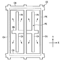
도 5는 본 실시 형태의 제1 구성예에 있어서의 액정 표시 패널(LPN)의 대향 기판(CT1)에 있어서의 1화소(PX)의 구조를 개략적으로 도시하는 평면도이다.Fig. 5 is a plan view schematically showing the structure of one pixel PX on the counter substrate CT1 of the liquid crystal display panel LPN in the first configuration example of the present embodiment.
이 제1 구성예에서는, 공통 전극(CE)은, 주공통 전극으로서 대향 기판(CT1)에 구비된 제2 주공통 전극(CA2) 및 부공통 전극으로서 대향 기판(CT1)에 구비된 제2 부공통 전극(CB2)을 갖고 있다. 이들 제2 주공통 전극(CA2) 및 제2 부공통 전극(CB2)은, 제2 배향막(AL2)에 의해 덮어져 있다.In this first configuration example, the common electrode CE includes a second main common electrode CA2 provided on the counter substrate CT1 as a main common electrode and a second main common electrode CA2 provided on the counter substrate CT1 as a sub- And has a common electrode CB2. The second main common electrode CA2 and the second sub-common electrode CB2 are covered with the second alignment film AL2.
즉, 도시한 대향 기판(CT1)은, 제2 방향(Y)을 따라 직선적으로 연장된 띠 형상의 제2 주공통 전극(CA2)과, 제1 방향(X)을 따라 직선적으로 연장된 띠 형상의 제2 부공통 전극(CB2)을 구비하고 있다. 이들 제2 주공통 전극(CA2) 및 제2 부공통 전극(CB2)은, 전기적으로 접속되어 있다. 도시한 예에서는, 제2 주공통 전극(CA2) 및 제2 부공통 전극(CB2)은, 일체적(혹은 연속적)으로 형성되어 있다. 즉, 대향 기판(CT1)에 있어서, 공통 전극(CE)은, 격자 형상으로 형성되어 있다.That is, the illustrated counter substrate CT1 includes a strip-shaped second main common electrode CA2 extending linearly along the second direction Y, and a strip-shaped second strip-like electrode extending linearly along the first direction X And a second sub-common electrode CB2. The second main common electrode CA2 and the second sub common electrode CB2 are electrically connected. In the illustrated example, the second main common electrode CA2 and the second sub common electrode CB2 are formed integrally (or continuously). That is, in the counter substrate CT1, the common electrode CE is formed in a lattice shape.
또한, 도시한 제2 주공통 전극(CA2)은 제1 방향(X)을 따라 간격을 두고 2개 평행하게 배열되어 있고, 이하에서는, 이들을 구별하기 위해, 도면 중의 좌측의 제2 주공통 전극을 CAL2라고 칭하고, 도면 중의 우측의 제2 주공통 전극을 CAR2라고 칭한다. 또한, 도시한 제2 부공통 전극(CB2)은 제2 방향(Y)을 따라 간격을 두고 2개 평행하게 배열되어 있고, 이하에서는, 이들을 구별하기 위해, 도면 중의 상측의 제2 부공통 전극을 CBU2라고 칭하고, 도면 중의 하측의 제2 부공통 전극을 CBB2라고 칭한다. 이들 제2 주공통 전극(CAL2) 및 제2 주공통 전극(CAR2)은, 제2 부공통 전극(CBU2) 및 제2 부공통 전극(CBB2)과 연결되어 있다.The second main common electrodes CA2 shown in the figure are arranged in parallel in parallel with each other along the first direction X. In order to distinguish them from each other, CAL2, and the second main common electrode on the right side in the figure is called CAR2. The illustrated second sub-common electrodes CB2 are arranged in parallel at intervals along the second direction Y. In order to distinguish the two sub-common electrodes CB2 from each other, the second sub- CBU2, and the lower second common electrode in the figure is called CBB2. The second main common electrode CAL2 and the second main common electrode CAR2 are connected to the second sub common electrode CBU2 and the second sub common electrode CBB2.
이러한 구성의 공통 전극(CE)은, 상술하지 않지만, 액티브 에어리어의 외측으로 인출되고, 도전 부재를 통해, 어레이 기판에 형성된 급전부와 전기적으로 접속되고, 공통 전위가 급전된다.The common electrode CE having such a configuration is drawn out to the outside of the active area, though not described in detail, and is electrically connected to the feeding part formed on the array substrate through the conductive member, and the common potential is fed.
다음으로, 도 5에 도시한 대향 기판(CT1)과의 조합이 적합한 어레이 기판(AR1)에 대해 설명한다.Next, an array substrate AR1 suitable for combination with the counter substrate CT1 shown in Fig. 5 will be described.
도 6은 본 실시 형태의 제1 구성예에 있어서의 액정 표시 패널(LPN)의 1화소(PX)를 대향 기판(CT1)측에서 보았을 때의 어레이 기판(AR1)의 구조를 개략적으로 도시하는 평면도이다. 또한, 화소 전극(PE)과 공통 전극(CE)과의 위치 관계를 설명하기 위해, 공통 전극(CE)을 파선으로 도시하고 있다. 또한, 1화소(PX)에 있어서의 설명에 필요한 구성만을 도시하고, 스위칭 소자 등의 도시를 생략하고 있다.6 is a plan view schematically showing the structure of the array substrate AR1 when one pixel PX of the liquid crystal display panel LPN in the first configuration example of the present embodiment is viewed from the counter substrate CT1 side to be. In order to explain the positional relationship between the pixel electrode PE and the common electrode CE, the common electrode CE is shown by a broken line. In addition, only the configuration necessary for the description of one pixel PX is shown, and the illustration of the switching elements and the like is omitted.
어레이 기판(AR1)은, 제1 방향(X)을 따라 연장된 보조 용량선(C1)과, 제1 방향(X)을 따라 연장된 게이트 배선(G1) 및 게이트 배선(G2)과, 제2 방향(Y)을 따라 연장된 소스 배선(S1) 및 소스 배선(S2)과, 화소 전극(PE)을 구비하고 있다. 보조 용량선(C1), 게이트 배선(G1) 및 게이트 배선(G2)은, 게이트 절연막(11) 상에 형성되고, 제1 층간 절연막(12)에 의해 덮어져 있다. 소스 배선(S1) 및 소스 배선(S2)은, 제1 층간 절연막(12) 상에 형성되고, 제2 층간 절연막(13)에 의해 덮어져 있다. 화소 전극(PE)은, 제2 층간 절연막(13) 상에 형성되어 있다.The array substrate AR1 includes a storage capacitor line C1 extending along the first direction X, a gate wiring G1 and a gate wiring G2 extending along the first direction X, A source wiring S1 and a source wiring S2 extending along the direction Y and a pixel electrode PE. The storage capacitor line C1, the gate wiring G1 and the gate wiring G2 are formed on the
도시한 예에서는, 화소(PX)는, 도면 중의 파선으로 나타낸 영역에 상당하고, 제1 방향(X)을 따른 길이보다도 제2 방향(Y)을 따른 길이 쪽이 긴 직사각 형상이다. 또한, 도시한 예에서는, 화소(PX)에 있어서, 소스 배선(S1)은 좌측 단부에 배치되고, 소스 배선(S2)은 우측 단부에 배치되어 있다. 엄밀하게는, 소스 배선(S1)은 당해 화소(PX)와 그 좌측에 인접하는 화소와의 경계에 걸쳐 배치되고, 소스 배선(S2)은 당해 화소(PX)와 그 우측에 인접하는 화소와의 경계에 걸쳐 배치되어 있다. 또한, 화소(PX)에 있어서, 게이트 배선(G1)은 상측 단부에 배치되고, 게이트 배선(G2)은 하측 단부에 배치되고, 보조 용량선(C1)은 대략 화소 중앙부에 배치되어 있다. 즉, 게이트 배선(G1)과 보조 용량선(C1)과의 제2 방향(Y)을 따른 간격은, 게이트 배선(G2)과 보조 용량선(C1)과의 제2 방향(Y)을 따른 간격과 대략 동등하다.In the illustrated example, the pixel PX corresponds to the area indicated by the broken line in the drawing, and has a rectangular shape with a longer length along the second direction Y than a length along the first direction X. In the illustrated example, in the pixel PX, the source wiring S1 is disposed at the left end portion, and the source wiring S2 is disposed at the right end portion. Strictly speaking, the source wiring S1 is arranged over the boundary between the pixel PX and the pixel adjacent to the pixel PX, and the source wiring S2 is arranged between the pixel PX and the pixel adjacent to the pixel PX Respectively. In the pixel PX, the gate line G1 is arranged at the upper end, the gate line G2 is arranged at the lower end, and the storage capacitor line C1 is arranged substantially at the center of the pixel. The interval between the gate line G1 and the storage capacitor line C1 along the second direction Y is equal to the interval between the gate line G2 and the storage capacitor line C1 in the second direction Y .
화소 전극(PE)은, 소스 배선(S1)과 소스 배선(S2)과의 사이, 혹은, 게이트 배선(G1)과 게이트 배선(G2)과의 사이에 배치되고, 도시를 생략한 스위칭 소자에 전기적으로 접속되어 있다. 이러한 화소 전극(PE)은, 제2 방향(Y)을 따라 직선적으로 연장된 띠 형상의 주화소 전극(PA) 및 제1 방향(X)을 따라 직선적으로 연장된 띠 형상의 부화소 전극(PB)을 갖고 있다. 이들 주화소 전극(PA) 및 부화소 전극(PB)은, 전기적으로 접속되어 있다. 도시한 예에서는, 주화소 전극(PA) 및 부화소 전극(PB)은, 일체적(혹은 연속적)으로 형성되어 있다. 즉, 어레이 기판(AR1)에 있어서, 화소 전극(PE)은, 십자 형상으로 형성되어 있다. 또한, 주화소 전극(PA) 및 부화소 전극(PB)은, 모두 제1 배향막(AL1)에 의해 덮어져 있다.The pixel electrode PE is disposed between the source wiring line S1 and the source wiring line S2 or between the gate wiring line G1 and the gate wiring line G2 and electrically connected to the switching elements Respectively. The pixel electrode PE includes a strip-shaped main pixel electrode PA linearly extending along the second direction Y and a strip-shaped sub-pixel electrode PB extending linearly along the first direction X ). The main pixel electrode PA and the sub-pixel electrode PB are electrically connected. In the illustrated example, the main pixel electrode PA and the sub-pixel electrode PB are formed integrally (or continuously). That is, in the array substrate AR1, the pixel electrode PE is formed in a cross shape. The main pixel electrode PA and the sub-pixel electrode PB are all covered with the first alignment film AL1.
주화소 전극(PA)은, 인접하는 소스 배선(S1) 및 소스 배선(S2)의 각각의 바로 위의 위치보다도 화소(PX)의 내측에 위치하고, 소스 배선(S1)과 소스 배선(S2)과의 대략 중간에 배치되어 있다. 이러한 주화소 전극(PA)은, 화소(PX)의 상측 단부 부근으로부터 하측 단부 부근까지 연장되어 있다.The main pixel electrode PA is located inside the pixel PX rather than immediately above each of the adjacent source wiring S1 and the source wiring S2 and the source wiring S1 and the source wiring S2, As shown in Fig. The main pixel electrode PA extends from the vicinity of the upper end of the pixel PX to the vicinity of the lower end.
부화소 전극(PB)은, 대략 화소 중앙부에 배치되고, 주화소 전극(PA)과 교차하고 있다. 이러한 부화소 전극(PB)은, 주화소 전극(PA)의 대략 중앙부로부터 그 양측, 즉, 주화소 전극(PA)의 좌측의 소스 배선(S1) 및 주화소 전극(PA)의 우측의 소스 배선(S2)을 향해 각각 직선적으로 연장되어 있다. 이러한 부화소 전극(PB)은, 화소(PX)의 좌측 단부 부근으로부터 우측 단부 부근까지 연장되어 있다.The sub-pixel electrode PB is arranged substantially at the center of the pixel and crosses the main pixel electrode PA. The sub-pixel electrode PB is connected to the source wiring S1 on the left side of the main pixel electrode PA and the source wiring S1 on the right side of the main pixel electrode PA from the substantially central portion of the main pixel electrode PA, (S2). The sub-pixel electrode PB extends from the vicinity of the left end of the pixel PX to the vicinity of the right end.
이 제1 구성예에 있어서는, 부화소 전극(PB)은, 보조 용량선(C1)과 대향하고 있다. 도시한 예에서는, 부화소 전극(PB)은, 보조 용량선(C1)의 상방에 배치되어 있다. 부화소 전극(PB)과 보조 용량선(C1)과의 사이에는, 절연막으로서, 제1 층간 절연막(12) 및 제2 층간 절연막(13)이 개재하고 있다.In the first configuration example, the sub-pixel electrode PB is opposed to the storage capacitor line C1. In the illustrated example, the sub-pixel electrode PB is arranged above the storage capacitor line C1. A first
이 부화소 전극(PB)의 제1 방향(X)을 따른 길이에 대해서는, 부화소 전극(PB)이 보조 용량선(C1)을 덮는 경우에는, 소스 배선(S1)과 소스 배선(S2)과의 사이에 위치하는 보조 용량선(C1)의 제1 방향(X)을 따른 길이와 동등 이상이다.The length along the first direction X of the sub-pixel electrode PB is set so that the distance between the source wiring S1 and the source wiring S2 becomes smaller when the sub- Is equal to or greater than the length along the first direction (X) of the storage capacitor line (C1) located between the first electrode
또한, 부화소 전극(PB)의 제2 방향(Y)을 따른 폭에 대해서는, 부화소 전극(PB)이 보조 용량선(C1) 상에서 도시하지 않은 스위칭 소자와 전기적으로 접속되는 구성의 경우, 비교적 폭 넓게 설정된다. 부화소 전극(PB)이 보조 용량선(C1)을 덮는 경우, 부화소 전극(PB)의 폭은 보조 용량선(C1)의 폭과 동등 이상이다.The width of the sub-pixel electrode PB along the second direction Y is relatively small in the case of a configuration in which the sub-pixel electrode PB is electrically connected to a switching element not shown on the storage capacitor line C1 Is set to be wide. When the sub-pixel electrode PB covers the storage capacitor line C1, the width of the sub-pixel electrode PB is equal to or greater than the width of the storage capacitor line C1.
상술한 바와 같이, 게이트 배선(G1)이 화소의 상측 단부에 배치되고, 보조 용량선(C1)이 대략 화소 중앙부에 배치된 구성에서는, 부화소 전극(PB)이 소스 배선(S1)과 소스 배선(S2)과의 사이에 위치하는 보조 용량선(C1)을 덮도록 배치 가능하다.As described above, in the configuration in which the gate line G1 is disposed at the upper end of the pixel and the storage capacitor line C1 is disposed approximately at the center of the pixel, the sub- And the storage capacitor line (S2).
또한, 보조 용량선(C1)이 화소(PX)의 상측 단부 또는 하측 단부에 배치되고, 게이트 배선(G1)이 대략 화소 중앙부에 배치되어도 된다. 이 경우에는, 부화소 전극(PB)은, 게이트 배선(G1)과 대향하고 있어도 된다[혹은, 부화소 전극(PB)이 게이트 배선(G1)의 상방에 배치되어 있어도 됨].The storage capacitor line C1 may be arranged at the upper end or the lower end of the pixel PX and the gate line G1 may be arranged substantially at the pixel center. In this case, the sub-pixel electrode PB may be opposed to the gate line G1 (or the sub-pixel electrode PB may be disposed above the gate line G1).
한편, 공통 전극(CE)에 있어서, 제2 주공통 전극(CAL2) 및 제2 주공통 전극(CAR2)은 주화소 전극(PA)의 바로 위의 위치를 사이에 둔 양측에 배치되고, 또한, 제2 부공통 전극(CBU2) 및 제2 부공통 전극(CBB2)은 부화소 전극(PB)의 바로 위의 위치를 사이에 둔 양측에 배치되어 있다. 환언하면, 주화소 전극(PA)은 제2 주공통 전극(CAL2)과 제2 주공통 전극(CAR2)과의 사이에 배치되고, 부화소 전극(PB)은 제2 부공통 전극(CBU2)과 제2 부공통 전극(CBB2)과의 사이에 배치되어 있다.On the other hand, in the common electrode CE, the second main common electrode CAL2 and the second main common electrode CAR2 are disposed on both sides with the position directly above the main pixel electrode PA therebetween, The second sub-common electrode CBU2 and the second sub-common electrode CBB2 are disposed on both sides with the position directly above the sub-pixel electrode PB therebetween. In other words, the main pixel electrode PA is disposed between the second main common electrode CAL2 and the second main common electrode CAR2, and the sub-pixel electrode PB is disposed between the second sub common electrode CBU2 and the second sub- And the second sub-common electrode CBB2.
도시한 예에서는, 제2 주공통 전극(CAL2)은, 화소(PX)의 좌측 단부에 배치되고, 소스 배선(S1)에 대향하고 있다[혹은, 제2 주공통 전극(CAL2)이 소스 배선(S1)의 상방에 배치되어 있음]. 또한, 제2 주공통 전극(CAR2)은, 화소(PX)의 우측 단부에 배치되고, 소스 배선(S2)에 대향하고 있다[혹은, 제2 주공통 전극(CAR2)이 소스 배선(S2)의 상방에 배치되어 있음]. 또한, 제2 부공통 전극(CBU2)은, 화소(PX)의 상측 단부에 배치되고, 게이트 배선(G1)에 대향하고 있다[혹은, 제2 부공통 전극(CBU2)이 게이트 배선(G1)의 상방에 배치되어 있음]. 또한, 제2 부공통 전극(CBB2)은, 화소(PX)의 하측 단부에 배치되고, 게이트 배선(G2)에 대향하고 있다[혹은, 제2 부공통 전극(CBB2)이 게이트 배선(G2)의 상방에 배치되어 있음].In the illustrated example, the second main common electrode CAL2 is disposed at the left end of the pixel PX and opposes the source wiring S1 (or the second main common electrode CAL2 is connected to the source wiring S1). The second main common electrode CAR2 is disposed at the right end of the pixel PX and opposes the source wiring S2 (or the second main common electrode CAR2 is connected to the source wiring S2) Is arranged above. The second sub common electrode CBU2 is disposed at the upper end of the pixel PX and opposes the gate wiring G1 Is arranged above. The second sub common electrode CBB2 is disposed at the lower end of the pixel PX and opposes the gate wiring G2 Is arranged above.
이러한 제1 구성예에 따르면, 상기한 바와 같이, 1화소 내에 4개의 도메인을 형성하는 것이 가능해지므로, 4방향에서의 시야각을 광학적으로 보상할 수 있어, 광시야각화가 가능해진다.According to the first configuration example, as described above, it is possible to form four domains in one pixel, so that it is possible to optically compensate the viewing angles in the four directions, thereby enabling a wide viewing angle.
또한, 제2 주공통 전극(CAL2) 및 제2 주공통 전극(CAR2)은, 각각 소스 배선(S1) 및 소스 배선(S2)과 대향하고 있다. 특히, 제2 주공통 전극(CAL2) 및 제2 주공통 전극(CAR2)이 각각 소스 배선(S1) 및 소스 배선(S2)의 상방에 배치되어 있는 경우에는, 제2 주공통 전극(CAL2) 및 제2 주공통 전극(CAR2)이 소스 배선(S1) 및 소스 배선(S2)보다도 주화소 전극(PA)측에 배치된 경우와 비교하여, 표시에 기여하는 개구부를 확대할 수 있어, 화소(PX)의 투과율을 향상시키는 것이 가능해진다.The second main common electrode CAL2 and the second main common electrode CAR2 face the source wiring S1 and the source wiring S2, respectively. Particularly when the second main common electrode CAL2 and the second main common electrode CAR2 are disposed above the source wiring S1 and the source wiring S2 respectively, The opening contributing to the display can be enlarged as compared with the case where the second main common electrode CAR2 is disposed closer to the main pixel electrode PA than the source wiring S1 and the source wiring S2, ) Can be improved.
또한, 제2 주공통 전극(CAL2) 및 제2 주공통 전극(CAR2)을 각각 소스 배선(S1) 및 소스 배선(S2)의 상방에 배치함으로써, 주화소 전극(PA)과 제2 주공통 전극(CAL2) 및 제2 주공통 전극(CAR2)과의 사이의 거리를 확대하는 것이 가능해지고, 보다 수평에 가까운 횡전계를 형성하는 것이 가능해진다. 이로 인해, 종래의 구성인 IPS 모드 등의 이점인 광시야각화도 유지하는 것이 가능해진다.The second main common electrode CAL2 and the second main common electrode CAR2 are disposed above the source wiring S1 and the source wiring S2 respectively so that the main pixel electrode PA and the second main common electrode It is possible to enlarge the distance between the second main common electrode CA2 and the second main common electrode CAR2, and to form a horizontal electric field closer to the horizontal. This makes it possible to maintain a wide viewing angle, which is an advantage of the conventional IPS mode and the like.
또한, 화소 전극(PE)의 부화소 전극(PB)은, 보조 용량선이나 게이트 배선과 대향하도록 배치되어 있으므로, 보조 용량선이나 게이트 배선으로부터의 원하지 않는 전계를 차폐하는 것이 가능해진다. 이로 인해, 보조 용량선이나 게이트 배선으로부터 액정층(LQ)에 대하여 원하지 않는 바이어스가 인가되는 것을 억제할 수 있고, 번인 등의 표시 불량의 발생을 억제하는 것이 가능해진다. 따라서, 더욱 표시 품위가 양호한 액정 표시 장치를 제공할 수 있다.In addition, since the sub-pixel electrode PB of the pixel electrode PE is disposed so as to face the storage capacitor line and the gate wiring, it is possible to shield an unwanted electric field from the storage capacitor line and the gate wiring. As a result, application of an undesired bias to the liquid crystal layer (LQ) from the storage capacitor line and the gate wiring can be suppressed, and occurrence of defective display such as burn-in can be suppressed. Therefore, it is possible to provide a liquid crystal display device with further improved display quality.
≪제2 구성예≫≪ Second Configuration Example &
다음으로, 본 실시 형태의 제2 구성예에 대해 설명한다. 또한, 제1 구성예와 동일 구성에 대해서는 동일한 참조 부호를 부여하여 상세한 설명을 생략한다.Next, a second configuration example of the present embodiment will be described. The same components as those in the first configuration are denoted by the same reference numerals, and a detailed description thereof will be omitted.
도 7은 본 실시 형태의 제2 구성예에 있어서의 액정 표시 패널(LPN)의 대향 기판(CT2)에 있어서의 1화소(PX)의 구조를 개략적으로 도시하는 평면도이다.7 is a plan view schematically showing the structure of one pixel PX on the counter substrate CT2 of the liquid crystal display panel LPN in the second configuration example of the present embodiment.
이 제2 구성예에서는, 공통 전극(CE)은, 주공통 전극으로서 후술하는 어레이 기판에 구비된 제1 주공통 전극(CA1) 및 부공통 전극으로서 대향 기판(CT2)에 구비된 제2 부공통 전극(CB2)을 갖고 있다. 이 제2 부공통 전극(CB2)은, 제2 배향막(AL2)에 의해 덮어져 있다.In this second configuration example, the common electrode CE includes a first main common electrode CA1 provided on an array substrate to be described later as a main common electrode and a second main common electrode CA1 provided on the counter substrate CT2 as a sub- And an electrode CB2. The second auxiliary common electrode CB2 is covered with a second alignment film AL2.
즉, 도시한 대향 기판(CT2)은, 제1 방향(X)을 따라 직선적으로 연장된 띠 형상의 제2 부공통 전극(CB2)을 구비하고 있고, 주공통 전극은 구비하고 있지 않다. 즉, 대향 기판(CT2)에 있어서, 공통 전극(CE)은, 제1 방향(X)으로 연장된 스트라이프 형상으로 형성되어 있다. 또한, 도시한 제2 부공통 전극(CB2)은 제2 방향(Y)을 따라 간격을 두고 2개 평행하게 배열되어 있고, 이하에서는, 이들을 구별하기 위해, 도면 중의 상측의 제2 부공통 전극을 CBU2라고 칭하고, 도면 중의 하측의 제2 부공통 전극을 CBB2라고 칭한다.That is, the illustrated counter substrate CT2 has a strip-shaped second sub-common electrode CB2 extending linearly along the first direction X, and does not include a main common electrode. That is, in the counter substrate CT2, the common electrode CE is formed in a stripe shape extending in the first direction X. The illustrated second sub-common electrodes CB2 are arranged in parallel at intervals along the second direction Y. In order to distinguish the two sub-common electrodes CB2 from each other, the second sub- CBU2, and the lower second common electrode in the figure is called CBB2.
이러한 공통 전극(CE)의 제2 부공통 전극(CB2)은, 상술하지 않지만, 액티브 에어리어의 외측으로 인출되고, 도전 부재를 통해, 어레이 기판에 형성된 급전부와 전기적으로 접속되고, 공통 전위가 급전된다.The second sub common electrode CB2 of the common electrode CE is drawn out to the outside of the active area and is electrically connected to the feeding part formed on the array substrate through the conductive member, do.
다음으로, 도 7에 도시한 대향 기판(CT2)과의 조합이 적합한 어레이 기판(AR2)에 대해 설명한다.Next, an array substrate AR2 suitable for combination with the counter substrate CT2 shown in Fig. 7 will be described.
도 8은 본 실시 형태의 제2 구성예에 있어서의 액정 표시 패널(LPN)의 1화소(PX)를 대향 기판(CT2)측에서 보았을 때의 어레이 기판(AR2)의 구조를 개략적으로 도시하는 평면도이다. 또한, 화소 전극(PE)과 공통 전극(CE)과의 위치 관계를 설명하기 위해, 공통 전극(CE)을 파선으로 도시하고 있다. 또한, 1화소(PX)에 있어서의 설명에 필요한 구성만을 도시하고, 스위칭 소자 등의 도시를 생략하고 있다.8 is a plan view schematically showing the structure of the array substrate AR2 when one pixel PX of the liquid crystal display panel LPN in the second configuration example of the present embodiment is viewed from the counter substrate CT2 side to be. In order to explain the positional relationship between the pixel electrode PE and the common electrode CE, the common electrode CE is shown by a broken line. In addition, only the configuration necessary for the description of one pixel PX is shown, and the illustration of the switching elements and the like is omitted.
어레이 기판(AR2)은, 어레이 기판(AR1)과 마찬가지로, 제1 방향(X)을 따라 연장된 보조 용량선(C1)과, 제1 방향(X)을 따라 연장된 게이트 배선(G1) 및 게이트 배선(G2)과, 제2 방향(Y)을 따라 연장된 소스 배선(S1) 및 소스 배선(S2)과, 화소 전극(PE)을 구비하고 있다. 화소 전극(PE)은, 제1 배향막(AL1)에 의해 덮어져 있다. 또한, 어레이 기판(AR2)은, 공통 전극(CE)의 일부로서, 제2 방향(Y)을 따라 직선적으로 연장된 띠 형상의 제1 주공통 전극(CA1)을 구비하고 있다. 이 제1 주공통 전극(CA1)은, 제2 부공통 전극(CB2)과 동일 전위이다.Like the array substrate AR1, the array substrate AR2 includes a storage capacitor line C1 extending along the first direction X, a gate wiring G1 extending along the first direction X, A wiring G2 and a source wiring S1 and a source wiring S2 extending along the second direction Y and a pixel electrode PE. The pixel electrode PE is covered with the first alignment film AL1. The array substrate AR2 has a strip-shaped first main common electrode CA1 extending linearly along the second direction Y as a part of the common electrode CE. The first main common electrode CA1 is at the same potential as the second sub common electrode CB2.
또한, 도시한 제1 주공통 전극(CA1)은 제1 방향(X)을 따라 간격을 두고 2개 평행하게 배열되어 있고, 이하에서는, 이들을 구별하기 위해, 도면 중의 좌측의 제1 주공통 전극을 CAL1이라고 칭하고, 도면 중의 우측의 제1 주공통 전극을 CAR1이라고 칭한다. 이들 제1 주공통 전극(CAL1) 및 제1 주공통 전극(CAR1)은, 예를 들어, 화소 전극(PE)과 마찬가지로, 제2 층간 절연막(13) 상에 형성되고, 제1 배향막(AL1)에 의해 덮어져 있다. 이 경우, 제1 주공통 전극(CAL1) 및 제1 주공통 전극(CAR1)은, 화소 전극(PE)과 동일 재료(예를 들어, ITO 등)를 사용하여 동일 공정에서 형성 가능하다.The first main common electrodes CA1 shown in the drawing are arranged in parallel at intervals along the first direction X. In order to distinguish them from each other, CAL1, and the first main common electrode on the right side in the figure is referred to as CAR1. The first main common electrode CAL1 and the first main common electrode CAR1 are formed on the second
도시한 예에서는, 제1 주공통 전극(CAL1)은, 화소(PX)의 좌측 단부에 배치되고, 소스 배선(S1)과 대향하고 있다[혹은, 제1 주공통 전극(CAL1)이 소스 배선(S1)의 상방에 배치되어 있음]. 또한, 제1 주공통 전극(CAR1)은, 화소(PX)의 우측 단부에 배치되고, 소스 배선(S2)과 대향하고 있다[혹은, 제1 주공통 전극(CAR1)이 소스 배선(S2)의 상방에 배치되어 있음]. 제1 주공통 전극(CAL1) 및 제1 주공통 전극(CAR1)과, 소스 배선(S1) 및 소스 배선(S2)과의 사이에는, 절연막으로서, 제2 층간 절연막(13)이 개재하고 있다.In the illustrated example, the first main common electrode CAL1 is disposed at the left end of the pixel PX and opposes the source wiring S1 (or the first main common electrode CAL1 is connected to the source wiring S1). The first main common electrode CAR1 is disposed at the right end of the pixel PX and opposes the source wiring S2 (or the first main common electrode CAR1 is connected to the source wiring S2) Is arranged above. A second
이들 제1 주공통 전극(CAL1) 및 제1 주공통 전극(CAR1)은, 각각 액티브 에어리어 내에 있어서는 직선적으로 연장되고, 액티브 에어리어의 외측으로 인출되고, 어레이 기판(AR2)에 형성된 급전부와 전기적으로 접속되고, 공통 전위가 급전된다. 또한, 제1 주공통 전극(CAL1) 및 제1 주공통 전극(CAR1)의 각각이 액티브 에어리어 내에 있어서 소스 배선(S1) 및 소스 배선(S2)을 덮는 경우에는, 제1 주공통 전극(CAL1) 및 제1 주공통 전극(CAR1)의 제1 방향(X)을 따른 폭에 대해서는, 소스 배선(S1) 및 소스 배선(S2)의 제1 방향(X)을 따른 폭과 동등 이상이다.The first main common electrode CAL1 and the first main common electrode CAR1 each extend linearly in the active area and are drawn out of the active area and electrically connected to the power feeding part formed on the array substrate AR2 And a common potential is supplied. When each of the first main common electrode CAL1 and the first main common electrode CAR1 covers the source wiring S1 and the source wiring S2 in the active area, the first main common electrode CAL1, And the width along the first direction X of the first main common electrode CAR1 are equal to or greater than the width along the first direction X of the source wiring S1 and the source wiring S2.
화소 전극(PE)은, 제1 구성예와 마찬가지로, 게이트 배선(G1)과 게이트 배선(G2)과의 사이에 배치되어 있다. 혹은, 화소 전극(PE)은, 소스 배선(S1)과 소스 배선(S2)과의 사이, 즉, 제1 주공통 전극(CAL1)과 제1 주공통 전극(CAR1)과의 사이에 배치되어 있다. 이 화소 전극(PE)은, 주화소 전극(PA) 및 부화소 전극(PB)을 갖고 있다.The pixel electrode PE is disposed between the gate wiring G1 and the gate wiring G2 in the same manner as in the first configuration example. Alternatively, the pixel electrode PE is disposed between the source wiring line S1 and the source wiring line S2, that is, between the first main common electrode CAL1 and the first main common electrode CAR1 . The pixel electrode PE has a main pixel electrode PA and a sub-pixel electrode PB.
주화소 전극(PA)은, 제1 주공통 전극(CAL1)과 제1 주공통 전극(CAR1)과의 대략 중간의 위치에 배치되어 있다. 이 주화소 전극(PA)은, 게이트 배선(G1) 및 게이트 배선(G2)을 향해 연장되어 있다.The main pixel electrode PA is disposed at a substantially intermediate position between the first main common electrode CAL1 and the first main common electrode CAR1. The main pixel electrode PA extends toward the gate wiring G1 and the gate wiring G2.
부화소 전극(PB)은, 게이트 배선(G1)과 게이트 배선(G2)과의 대략 중간의 위치에 배치되어 있다. 이 부화소 전극(PB)은, 제1 주공통 전극(CAL1) 및 제1 주공통 전극(CAR1)을 향해 연장되어 있다. 단, 화소 전극(PE)이 제1 주공통 전극(CAL1) 및 제1 주공통 전극(CAR1)과 함께 제2 층간 절연막(13) 상에 형성되어 있는 경우에는, 부화소 전극(PB)은, 제1 주공통 전극(CAL1) 및 제1 주공통 전극(CAR1)에는 접촉하지 않도록 배치되어 있다[혹은, 부화소 전극(PB)이 제1 주공통 전극(CAL1) 및 제1 주공통 전극(CAR1)으로부터 이격되도록 배치되어 있음]. 또한, 이 부화소 전극(PB)은, 보조 용량선(C1)과 대향하고 있다[혹은, 부화소 전극(PB)이 보조 용량선(C1)의 상방에 배치되어 있음].The sub-pixel electrode PB is disposed at a position substantially intermediate between the gate wiring G1 and the gate wiring G2. The sub-pixel electrode PB extends toward the first main common electrode CAL1 and the first main common electrode CAR1. However, in the case where the pixel electrode PE is formed on the second
또한, 보조 용량선(C1)이 화소(PX)의 상측 단부 또는 하측 단부에 배치되고, 게이트 배선(G1)이 대략 화소 중앙부에 배치되어도 된다. 이 경우에는, 부화소 전극(PB)은, 게이트 배선(G1)과 대향하고 있어도 된다[혹은, 부화소 전극(PB)이 게이트 배선(G1)의 상방에 배치되어 있어도 됨].The storage capacitor line C1 may be arranged at the upper end or the lower end of the pixel PX and the gate line G1 may be arranged substantially at the pixel center. In this case, the sub-pixel electrode PB may be opposed to the gate line G1 (or the sub-pixel electrode PB may be disposed above the gate line G1).
한편, 공통 전극(CE)에 있어서, 제2 부공통 전극(CBU2) 및 제2 부공통 전극(CBB2)은, 부화소 전극(PB)의 바로 위의 위치를 사이에 둔 양측에 배치되어 있다. 환언하면, 주화소 전극(PA)은 제1 주공통 전극(CAL1)과 제1 주공통 전극(CAR1)과의 사이에 배치되고, 부화소 전극(PB)은 제2 부공통 전극(CBU2)과 제2 부공통 전극(CBB2)과의 사이에 배치되어 있다.On the other hand, in the common electrode CE, the second sub-common electrode CBU2 and the second sub-common electrode CBB2 are disposed on both sides with the position immediately above the sub-pixel electrode PB therebetween. In other words, the main pixel electrode PA is disposed between the first main common electrode CAL1 and the first main common electrode CAR1, the sub-pixel electrode PB is connected to the second sub common electrode CBU2, And the second sub-common electrode CBB2.
도시한 예에서는, 제2 부공통 전극(CBU2)은, 화소(PX)의 상측 단부에 배치되고, 게이트 배선(G1)에 대향하고 있다[혹은, 제2 부공통 전극(CBU2)이 게이트 배선(G1)의 상방에 배치되어 있음]. 또한, 제2 부공통 전극(CBB2)은, 화소(PX)의 하측 단부에 배치되고, 게이트 배선(G2)에 대향하고 있다[혹은, 제2 부공통 전극(CBB2)이 게이트 배선(G2)의 상방에 배치되어 있음].In the illustrated example, the second sub common electrode CBU2 is disposed at the upper end of the pixel PX and opposes the gate wiring G1 (or the second sub common electrode CBU2 is connected to the gate wiring 0.0 > G1). ≪ / RTI > The second sub common electrode CBB2 is disposed at the lower end of the pixel PX and opposes the gate wiring G2 Is arranged above.
이러한 제2 구성예에 따르면, 상기한 바와 같이, 1화소 내에 4개의 도메인을 형성하는 것이 가능해지므로, 4방향에서의 시야각을 광학적으로 보상할 수 있어, 광시야각화가 가능해진다. 또한, 제1 구성예에서 설명한 효과 외에, 공통 전극(CE)의 제1 주공통 전극(CA1)의 적어도 1개는, 소스 배선과 대향하도록 배치되어 있으므로, 소스 배선으로부터의 원하지 않는 전계를 차폐하는 것이 가능해진다. 이로 인해, 소스 배선으로부터 액정층(LQ)에 대하여 원하지 않는 바이어스가 인가되는 것을 억제할 수 있고, 크로스 토크[예를 들어, 당해 화소(PX)가 흑색을 표시하는 화소 전위로 설정되어 있는 상태에서, 당해 화소(PX)에 접속된 소스 배선에 백색을 표시하는 화소 전위가 공급되었을 때에, 당해 화소(PX)의 일부로부터 광 누설이 발생하여 휘도의 상승을 초래하는 현상] 등의 표시 불량의 발생을 억제하는 것이 가능해진다. 따라서, 더욱 표시 품위가 양호한 액정 표시 장치를 제공할 수 있다.According to the second configuration example, as described above, it is possible to form four domains in one pixel, so that it is possible to optically compensate the viewing angles in the four directions, thereby making it possible to realize a wide viewing angle. In addition to the effects described in the first configuration example, since at least one of the first main common electrodes CA1 of the common electrode CE is arranged to face the source wiring, it is possible to prevent unwanted electric fields Lt; / RTI > As a result, application of an undesired bias to the liquid crystal layer LQ from the source wiring can be suppressed. In the state where the crosstalk (for example, the pixel PX is set to the pixel potential for displaying black) , A phenomenon in which light leakage occurs from a part of the pixel PX to cause a rise in luminance when a pixel potential for displaying white is supplied to the source wiring connected to the pixel PX] Can be suppressed. Therefore, it is possible to provide a liquid crystal display device with further improved display quality.
또한, 이 제2 구성예에서 설명한 어레이 기판(AR2)은, 제1 구성예에서 설명한 대향 기판(CT1)과 조합해도 된다. 이 경우, 공통 전극(CE)은, 주공통 전극으로서, 어레이 기판(AR2)에 구비된 제1 주공통 전극(CA1) 및 대향 기판(CT1)에 구비된 제2 주공통 전극(CA2)을 갖는 구성으로 된다. 이러한 제1 주공통 전극(CA1)과 제2 주공통 전극(CA2)이 액정층을 사이에 두어 대향하는 영역에서는, 원하지 않는 종전계(즉, 기판 주면의 법선 방향을 따른 전계)의 발생을 억제하는 것이 가능해진다.The array substrate AR2 described in the second configuration example may be combined with the counter substrate CT1 described in the first configuration example. In this case, the common electrode CE has the first main common electrode CA1 provided on the array substrate AR2 and the second main common electrode CA2 provided on the counter substrate CT1 as the main common electrode . In the region where the first main common electrode CA1 and the second main common electrode CA2 face each other with the liquid crystal layer therebetween, an undesired current collector (that is, an electric field along the normal direction of the main surface of the substrate) .
≪제3 구성예≫«Third Configuration Example»
다음으로, 본 실시 형태의 제3 구성예에 대해 설명한다. 또한, 제1 구성예와 동일 구성에 대해서는 동일한 참조 부호를 부여하여 상세한 설명을 생략한다.Next, a third configuration example of the present embodiment will be described. The same components as those in the first configuration are denoted by the same reference numerals, and a detailed description thereof will be omitted.
도 9는 본 실시 형태의 제3 구성예에 있어서의 액정 표시 패널(LPN)의 대향 기판(CT3)에 있어서의 1화소(PX)의 구조를 개략적으로 도시하는 평면도이다.9 is a plan view schematically showing the structure of one pixel PX on the counter substrate CT3 of the liquid crystal display panel LPN in the third exemplary configuration of the present embodiment.
이 제3 구성예에서는, 공통 전극(CE)은, 주공통 전극으로서 대향 기판(CT3)에 구비된 제2 주공통 전극(CA2) 및 부공통 전극으로서 후술하는 어레이 기판에 구비된 제1 부공통 전극(CB1)을 갖고 있다. 이 제2 주공통 전극(CA2)은, 제2 배향막(AL2)에 의해 덮어져 있다.In this third configuration example, the common electrode CE includes a second main common electrode CA2 provided on the counter substrate CT3 as a main common electrode and a first main common electrode CA2 provided on the array substrate And an electrode CB1. This second main common electrode CA2 is covered with the second alignment film AL2.
즉, 도시한 대향 기판(CT3)은, 제2 방향(Y)을 따라 직선적으로 연장된 띠 형상의 제2 주공통 전극(CA2)을 구비하고 있고, 부공통 전극은 구비하고 있지 않다. 즉, 대향 기판(CT3)에 있어서, 공통 전극(CE)은, 제2 방향(Y)으로 연장된 스트라이프 형상으로 형성되어 있다. 또한, 도시한 제2 주공통 전극(CA2)은 제1 방향(X)을 따라 간격을 두고 2개 평행하게 배열되어 있고, 이하에서는, 이들을 구별하기 위해, 도면 중의 좌측의 제2 주공통 전극을 CAL2라고 칭하고, 도면 중의 우측의 제2 주공통 전극을 CAR2라고 칭한다.That is, the illustrated counter substrate CT3 has a strip-shaped second main common electrode CA2 extending linearly along the second direction Y, and does not include a sub common electrode. That is, in the counter substrate CT3, the common electrode CE is formed in a stripe shape extending in the second direction Y. The second main common electrodes CA2 shown in the figure are arranged in parallel in parallel with each other along the first direction X. In order to distinguish them from each other, CAL2, and the second main common electrode on the right side in the figure is called CAR2.
이러한 공통 전극(CE)의 제2 주공통 전극(CA2)은, 상술하지 않지만, 액티브 에어리어의 외측으로 인출되고, 도전 부재를 통해, 어레이 기판에 형성된 급전부와 전기적으로 접속되고, 공통 전위가 급전된다.Although not described in detail, the second main common electrode CA2 of the common electrode CE is drawn out to the outside of the active area and is electrically connected to the feeding part formed on the array substrate through the conductive member, do.
다음으로, 도 9에 도시한 대향 기판(CT3)과의 조합이 적합한 어레이 기판(AR3)에 대해 설명한다.Next, an array substrate AR3 suitable for combination with the counter substrate CT3 shown in Fig. 9 will be described.
도 10은 본 실시 형태의 제3 구성예에 있어서의 액정 표시 패널(LPN)의 1화소(PX)를 대향 기판(CT3)의 측에서 보았을 때의 어레이 기판(AR3)의 구조를 개략적으로 도시하는 평면도이다. 또한, 화소 전극(PE)과 공통 전극(CE)과의 위치 관계를 설명하기 위해, 공통 전극(CE)을 파선으로 도시하고 있다. 또한, 1화소(PX)에 있어서의 설명에 필요한 구성만을 도시하고, 스위칭 소자 등의 도시를 생략하고 있다.10 schematically shows the structure of the array substrate AR3 when one pixel PX of the liquid crystal display panel LPN in the third configuration example of the present embodiment is viewed from the side of the counter substrate CT3 FIG. In order to explain the positional relationship between the pixel electrode PE and the common electrode CE, the common electrode CE is shown by a broken line. In addition, only the configuration necessary for the description of one pixel PX is shown, and the illustration of the switching elements and the like is omitted.
어레이 기판(AR3)은, 어레이 기판(AR1)과 마찬가지로, 제1 방향(X)을 따라 연장된 보조 용량선(C1)과, 제1 방향(X)을 따라 연장된 게이트 배선(G1) 및 게이트 배선(G2)과, 제2 방향(Y)을 따라 연장된 소스 배선(S1) 및 소스 배선(S2)과, 화소 전극(PE)을 구비하고 있다. 화소 전극(PE)은, 제1 배향막(AL1)에 의해 덮어져 있다. 또한, 어레이 기판(AR3)은, 공통 전극(CE)의 일부로서, 제1 방향(X)을 따라 직선적으로 연장된 띠 형상의 제1 부공통 전극(CB1)을 구비하고 있다. 이 제1 부공통 전극(CB1)은, 제2 주공통 전극(CA2)과 동일 전위이다.Like the array substrate AR1, the array substrate AR3 includes a storage capacitor line C1 extending along the first direction X, a gate wiring G1 extending along the first direction X, A wiring G2 and a source wiring S1 and a source wiring S2 extending along the second direction Y and a pixel electrode PE. The pixel electrode PE is covered with the first alignment film AL1. The array substrate AR3 has a strip-shaped first sub-common electrode CB1 extending linearly along the first direction X as a part of the common electrode CE. The first sub common electrode CB1 is at the same potential as the second main common electrode CA2.
또한, 도시한 제1 부공통 전극(CB1)은 제2 방향(Y)을 따라 간격을 두고 2개 평행하게 배열되어 있고, 이하에서는, 이들을 구별하기 위해, 도면 중의 상측의 제1 부공통 전극을 CBU1이라고 칭하고, 도면 중의 하측의 제1 부공통 전극을 CBB1이라고 칭한다. 이들 제1 부공통 전극(CBU1) 및 제1 부공통 전극(CBB1)은, 예를 들어, 화소 전극(PE)과 마찬가지로, 제2 층간 절연막(13) 상에 형성되고, 제1 배향막(AL1)에 의해 덮어져 있다. 이 경우, 제1 부공통 전극(CBU1) 및 제1 부공통 전극(CBB1)은, 화소 전극(PE)과 동일 재료(예를 들어, ITO 등)를 사용하여 동일 공정에서 형성 가능하다.The illustrated first sub-common electrodes CB1 are arranged in parallel at intervals along the second direction Y. In order to distinguish them from each other, the first sub- CBU1, and the first sub-common electrode on the lower side in the figure is referred to as CBB1. The first sub-common electrode CBU1 and the first sub-common electrode CBB1 are formed on the second
도시한 예에서는, 제1 부공통 전극(CBU1)은, 화소(PX)의 상측 단부에 배치되고, 게이트 배선(G1)과 대향하고 있다[혹은, 제1 부공통 전극(CBU1)이 게이트 배선(G1)의 상방에 배치되어 있음]. 또한, 제1 부공통 전극(CBB1)은, 화소(PX)의 하측 단부에 배치되고, 게이트 배선(G2)과 대향하고 있다[혹은, 제1 부공통 전극(CBB1)이 게이트 배선(G2)의 상방에 배치되어 있음]. 제1 부공통 전극(CBU1) 및 제1 부공통 전극(CBB1)과, 게이트 배선(G1) 및 게이트 배선(G2)과의 사이에는, 절연막으로서, 제1 층간 절연막(12) 및 제2 층간 절연막(13)이 개재하고 있다.In the illustrated example, the first sub common electrode CBU1 is disposed at the upper end of the pixel PX and opposes the gate wiring G1 (or the first sub common electrode CBU1 is connected to the gate wiring 0.0 > G1). ≪ / RTI > The first sub common electrode CBB1 is disposed at the lower end of the pixel PX and opposes the gate wiring G2 Is arranged above. A first
이들 제1 부공통 전극(CBU1) 및 제1 부공통 전극(CBB1)은, 각각 액티브 에어리어 내에 있어서는 직선적으로 연장되고, 액티브 에어리어의 외측으로 인출되고, 어레이 기판(AR3)에 형성된 급전부와 전기적으로 접속되고, 공통 전위가 급전된다. 또한, 제1 부공통 전극(CBU1) 및 제1 부공통 전극(CBB1)의 각각이 액티브 에어리어 내에 있어서 게이트 배선(G1) 및 게이트 배선(G2)을 덮는 경우에는, 제1 부공통 전극(CBU1) 및 제1 부공통 전극(CBB1)의 제2 방향(Y)을 따른 폭에 대해서는, 게이트 배선(G1) 및 게이트 배선(G2)의 제2 방향(Y)을 따른 폭과 동등 이상이다.Each of the first sub-common electrode CBU1 and the first sub-common electrode CBB1 extends linearly in the active area and is drawn out of the active area and electrically connected to the power supply part formed on the array substrate AR3 And a common potential is supplied. When each of the first sub-common electrode CBU1 and the first sub-common electrode CBB1 covers the gate wiring G1 and the gate wiring G2 in the active area, the first sub- And the width along the second direction Y of the first sub common electrode CBB1 are equal to or more than the width along the second direction Y of the gate wiring G1 and the gate wiring G2.
화소 전극(PE)은, 제1 구성예와 마찬가지로, 소스 배선(S1)과 소스 배선(S2)과의 사이에 배치되어 있다. 혹은, 화소 전극(PE)은, 게이트 배선(G1)과 게이트 배선(G2)과의 사이, 즉, 제1 부공통 전극(CBU1)과 제1 부공통 전극(CBB1)과의 사이에 배치되어 있다. 이 화소 전극(PE)은, 주화소 전극(PA) 및 부화소 전극(PB)을 갖고 있다.The pixel electrode PE is disposed between the source wiring line S1 and the source wiring line S2 in the same manner as in the first configuration example. Alternatively, the pixel electrode PE is disposed between the gate line G1 and the gate line G2, that is, between the first sub-common electrode CBU1 and the first sub-common electrode CBB1 . The pixel electrode PE has a main pixel electrode PA and a sub-pixel electrode PB.
주화소 전극(PA)은, 소스 배선(S1)과 소스 배선(S2)과의 대략 중간의 위치에 배치되어 있다. 이 주화소 전극(PA)은, 제1 부공통 전극(CBU1) 및 제1 부공통 전극(CBB1)을 향해 연장되어 있다. 단, 화소 전극(PE)이 제1 부공통 전극(CBU1) 및 제1 부공통 전극(CBB1)과 함께 제2 층간 절연막(13) 상에 형성되어 있는 경우에는, 주화소 전극(PA)은, 제1 부공통 전극(CBU1) 및 제1 부공통 전극(CBB1)에는 접촉하지 않도록 배치되어 있다[혹은, 주화소 전극(PA)이 제1 부공통 전극(CBU1) 및 제1 부공통 전극(CBB1)으로부터 이격되도록 배치되어 있음].The main pixel electrode PA is arranged substantially at the intermediate position between the source wiring S1 and the source wiring S2. The main pixel electrode PA extends toward the first sub common electrode CBU1 and the first sub common electrode CBB1. When the pixel electrode PE is formed on the second
부화소 전극(PB)은, 제1 부공통 전극(CBU1)과 제1 부공통 전극(CBB1)과 대략 중간의 위치에 배치되어 있다. 이 부화소 전극(PB)은, 소스 배선(S1) 및 소스 배선(S2)을 향해 연장되어 있다. 또한, 이 부화소 전극(PB)은, 보조 용량선(C1)과 대향하고 있다[혹은, 부화소 전극(PB)이 보조 용량선(C1)의 상방에 배치되어 있음].The sub-pixel electrode PB is disposed at a substantially intermediate position between the first sub-common electrode CBU1 and the first sub-common electrode CBB1. The sub-pixel electrode PB extends toward the source wiring S1 and the source wiring S2. The sub-pixel electrode PB is opposed to the storage capacitor line C1 (or the sub-pixel electrode PB is disposed above the storage capacitor line C1).
또한, 보조 용량선(C1)이 화소(PX)의 상측 단부 또는 하측 단부에 배치되고, 게이트 배선(G1)이 대략 화소 중앙부에 배치되어도 된다. 이 경우에는, 부화소 전극(PB)은, 게이트 배선(G1)과 대향하고 있어도 되고[혹은, 부화소 전극(PB)이 게이트 배선(G1)의 상방에 배치되어 있어도 되고], 제1 부공통 전극(CBU1) 또는 제1 부공통 전극(CBB1)은, 보조 용량선(C1)과 대향하고 있어도 된다[혹은, 제1 부공통 전극(CBU1) 또는 제1 부공통 전극(CBB1)이 보조 용량선(C1)의 상방에 배치되어 있어도 됨].The storage capacitor line C1 may be arranged at the upper end or the lower end of the pixel PX and the gate line G1 may be arranged substantially at the pixel center. In this case, the sub-pixel electrode PB may be opposed to the gate line G1 (or the sub-pixel electrode PB may be disposed above the gate line G1) The electrode CBU1 or the first sub common electrode CBB1 may be opposed to the auxiliary capacitance line C1 (or the first sub common electrode CBU1 or the first sub common electrode CBB1 may be opposed to the auxiliary capacitance line C1) (Which may be disposed above the first electrode C1).
한편, 공통 전극(CE)에 있어서, 제2 주공통 전극(CAL2) 및 제2 주공통 전극(CAR2)은, 주화소 전극(PA)의 바로 위의 위치를 사이에 둔 양측에 배치되어 있다. 환언하면, 주화소 전극(PA)은 제2 주공통 전극(CAL2)과 제2 주공통 전극(CAR2)과의 사이에 배치되고, 부화소 전극(PB)은 제1 부공통 전극(CBU1)과 제1 부공통 전극(CBB1)과의 사이에 배치되어 있다.On the other hand, in the common electrode CE, the second main common electrode CAL2 and the second main common electrode CAR2 are disposed on both sides with the position directly above the main pixel electrode PA therebetween. In other words, the main pixel electrode PA is disposed between the second main common electrode CAL2 and the second main common electrode CAR2, and the sub-pixel electrode PB is disposed between the first sub common electrode CBU1 and the first sub- And the first sub-common electrode CBB1.
도시한 예에서는, 제2 주공통 전극(CAL2)은, 화소(PX)의 좌측 단부에 배치되고, 소스 배선(S1)과 대향하고 있다[혹은, 제2 주공통 전극(CAL2)이 소스 배선(S1)의 상방에 배치되어 있음]. 또한, 제2 주공통 전극(CAR2)은, 화소(PX)의 우측 단부에 배치되고, 소스 배선(S2)과 대향하고 있다[혹은, 제2 주공통 전극(CAR2)이 소스 배선(S2)의 상방에 배치되어 있음].In the illustrated example, the second main common electrode CAL2 is disposed at the left end of the pixel PX and opposes the source wiring S1 (or the second main common electrode CAL2 is connected to the source wiring S1). The second main common electrode CAR2 is disposed at the right end of the pixel PX and opposes the source wiring S2 Is arranged above.
이러한 제3 구성예에 따르면, 상기한 바와 같이, 1화소 내에 4개의 도메인을 형성하는 것이 가능해지므로, 4방향에서의 시야각을 광학적으로 보상할 수 있어, 광시야각화가 가능해진다. 또한, 제1 구성예에서 설명한 효과 외에, 공통 전극(CE)의 제1 부공통 전극(CB1)은, 게이트 배선과 대향하도록 배치되어 있으므로, 게이트 배선으로부터의 원하지 않는 전계를 차폐하는 것이 가능해진다. 이로 인해, 게이트 배선으로부터 액정층(LQ)에 대하여 원하지 않는 바이어스가 인가되는 것을 억제할 수 있고, 번인 등의 표시 불량의 발생을 억제하는 것이 가능해진다. 따라서, 더욱 표시 품위가 양호한 액정 표시 장치를 제공할 수 있다.According to the third configuration example, as described above, it is possible to form four domains in one pixel, so that it is possible to optically compensate the viewing angles in the four directions, thereby enabling a wide viewing angle. In addition to the effects described in the first structural example, since the first sub-common electrode CB1 of the common electrode CE is arranged to face the gate wiring, it is possible to shield an unwanted electric field from the gate wiring. As a result, application of an undesired bias to the liquid crystal layer (LQ) from the gate wiring can be suppressed, and occurrence of defective display such as burn-in can be suppressed. Therefore, it is possible to provide a liquid crystal display device with further improved display quality.
또한, 이 제3 구성예에서 설명한 어레이 기판(AR3)은, 제1 구성예에서 설명한 대향 기판(CT1)과 조합해도 된다. 이 경우, 공통 전극(CE)은, 부공통 전극으로서, 어레이 기판(AR3)에 구비된 제1 부공통 전극(CB1) 및 대향 기판(CT1)에 구비된 제2 부공통 전극(CB2)을 갖는 구성으로 된다. 이러한 제1 부공통 전극(CB1)과 제2 부공통 전극(CB2)이 액정층을 사이에 두어 대향하는 영역에서는, 원하지 않는 종전계(즉, 기판 주면의 법선 방향을 따른 전계)의 발생을 억제하는 것이 가능해진다.The array substrate AR3 described in the third configuration example may be combined with the counter substrate CT1 described in the first configuration example. In this case, the common electrode CE has a first sub-common electrode CB1 provided on the array substrate AR3 and a second sub-common electrode CB2 provided on the counter substrate CT1 as a sub-common electrode . In the region where the first sub-common electrode CB1 and the second sub-common electrode CB2 face each other with the liquid crystal layer therebetween, an undesired electric field system (i.e., an electric field along the normal direction of the substrate main surface) is suppressed .
≪제4 구성예≫≪ Fourth Configuration Example &
다음으로, 본 실시 형태의 제4 구성예에 대해 설명한다. 또한, 제1 구성예와 동일 구성에 대해서는 동일한 참조 부호를 부여하여 상세한 설명을 생략한다.Next, a fourth configuration example of the present embodiment will be described. The same components as those in the first configuration are denoted by the same reference numerals, and a detailed description thereof will be omitted.
도 11은 본 실시 형태의 제4 구성예에 있어서의 액정 표시 패널(LPN)의 1화소(PX)를 대향 기판(CT)의 측에서 보았을 때의 어레이 기판(AR4)의 구조를 개략적으로 도시하는 평면도이다. 또한, 1화소(PX)에 있어서의 설명에 필요한 구성만을 도시하고, 스위칭 소자 등의 도시를 생략하고 있다.11 schematically shows the structure of the array substrate AR4 when one pixel PX of the liquid crystal display panel LPN in the fourth exemplary configuration of the present embodiment is viewed from the side of the counter substrate CT FIG. In addition, only the configuration necessary for the description of one pixel PX is shown, and the illustration of the switching elements and the like is omitted.
이 제4 구성예에서는, 공통 전극(CE)은, 주공통 전극으로서 어레이 기판(AR4)에 구비된 제1 주공통 전극(CA1) 및 부공통 전극으로서 어레이 기판(AR4)에 구비된 제1 부공통 전극(CB1)을 갖고 있다.In the fourth configuration example, the common electrode CE includes a first main common electrode CA1 provided on the array substrate AR4 as a main common electrode and a first main common electrode CA1 provided on the array substrate AR4 as a sub- And has a common electrode CB1.
어레이 기판(AR4)은, 어레이 기판(AR1)과 마찬가지로, 제1 방향(X)을 따라 연장된 보조 용량선(C1)과, 제1 방향(X)을 따라 연장된 게이트 배선(G1) 및 게이트 배선(G2)과, 제2 방향(Y)을 따라 연장된 소스 배선(S1) 및 소스 배선(S2)과, 화소 전극(PE)을 구비하고 있다. 화소 전극(PE)은, 제1 배향막(AL1)에 의해 덮어져 있다. 또한, 어레이 기판(AR4)은, 제2 방향(Y)을 따라 직선적으로 연장된 띠 형상의 제1 주공통 전극(CA1)(CAL1 및 CAR1) 및 제1 방향(X)을 따라 직선적으로 연장된 띠 형상의 제1 부공통 전극(CB1)(CBU1 및 CBB1)을 갖는 공통 전극(CE)을 구비하고 있다. 즉, 어레이 기판(AR4)에 있어서, 공통 전극(CE)은, 격자 형상으로 형성되어 있다. 제1 주공통 전극(CA1)의 구성에 대해서는, 어레이 기판(AR2)에서 설명한 바와 같다. 제1 부공통 전극(CB1)의 구성에 대해서는, 어레이 기판(AR3)에서 설명한 바와 같다.Like the array substrate AR1, the array substrate AR4 includes a storage capacitor line C1 extending along the first direction X, a gate wiring G1 extending along the first direction X, A wiring G2 and a source wiring S1 and a source wiring S2 extending along the second direction Y and a pixel electrode PE. The pixel electrode PE is covered with the first alignment film AL1. The array substrate AR4 further includes a strip-shaped first main common electrode CA1 (CAL1 and CAR1) extending linearly along the second direction Y and a first main common electrode CA2 extending linearly along the first direction X And a common electrode CE having strip-shaped first sub-common electrodes CB1 (CBU1 and CBB1). That is, in the array substrate AR4, the common electrode CE is formed in a lattice shape. The structure of the first main common electrode CA1 is as described for the array substrate AR2. The structure of the first sub-common electrode CB1 is as described for the array substrate AR3.
이러한 공통 전극(CE)의 제1 주공통 전극(CA1) 및 제1 부공통 전극(CB1)은, 상술하지 않지만, 액티브 에어리어의 외측으로 인출되고, 도전 부재를 통해, 어레이 기판(AR4)에 형성된 급전부와 전기적으로 접속되고, 공통 전위가 급전된다.Although not described in detail, the first main common electrode CA1 and the first sub common electrode CB1 of the common electrode CE are drawn out to the outside of the active area and are formed on the array substrate AR4 through the conductive member And is electrically connected to the power feeding portion, and a common potential is supplied.
이 제4 구성예에서 설명한 어레이 기판(AR4)은, 제1 구성예에서 설명한 대향 기판(CT1), 제2 구성예에서 설명한 대향 기판(CT2) 및 제3 구성예에서 설명한 대향 기판(CT3)의 어느 것과도 조합 가능하다.The array substrate AR4 described in the fourth configuration example is the same as the array substrate AR1 described in the first configuration example, the counter substrate CT2 described in the second configuration example, and the counter substrate CT3 described in the third configuration example It can be combined with any.
상기한 제1 내지 제4 구성예에서 설명한 어레이 기판(AR1), 어레이 기판(AR2), 어레이 기판(AR3) 및 어레이 기판(AR4)과, 상기한 제1 내지 제3 구성예에서 설명한 대향 기판(CT1), 대향 기판(CT2) 및 대향 기판(CT3)과의 조합에 대해서는, 도 12에 정리하였다. 도면 중의 사선은 본 실시 형태의 기본 구성을 실현할 수 없는 조합에 상당하고, 도면 중의 이중원(◎)은 각 구성예에서 설명한 조합에 상당하고, 도면 중의 백색 원(○)은 각 구성예에 있어서 가능한 조합에 상당한다.The array substrate AR1, the array substrate AR2, the array substrate AR3 and the array substrate AR4 described in the first to fourth structural examples described above and the counter substrate CT1, the counter substrate CT2 and the counter substrate CT3 are summarized in Fig. The hatched lines in the figure correspond to combinations that can not realize the basic configuration of the present embodiment. The double circle (& cir &) in the figure corresponds to the combination described in each of the configuration examples. Correspond to a combination.
다음으로, 본 실시 형태의 다른 배리에이션에 대해 1화소(PX)의 구성을 간단하게 설명한다.Next, the configuration of one pixel (PX) will be briefly described with respect to other variations of the present embodiment.
도 13은 본 실시 형태의 배리에이션의 하나를 개략적으로 도시하는 평면도이다.13 is a plan view schematically showing one variation of this embodiment.
화소 전극(PE)은, 제2 방향(Y)을 따라 연장되고 또한 제1 방향(X)을 따라 간격을 두고 평행하게 배열된 2개의 주화소 전극(PA), 제1 방향(X)을 따라 연장되고 또한 2개의 주화소 전극(PA)과 교차함과 함께 대략 화소 중앙부에 배치된 부화소 전극(PB)을 갖고 있다. 이러한 화소 전극(PE)은, 어레이 기판에 구비되어 있다.The pixel electrodes PE include two main pixel electrodes PA extending in the second direction Y and arranged in parallel with a spacing along the first direction X, And a sub-pixel electrode PB extending substantially in the center of the pixel while intersecting the two main pixel electrodes PA. These pixel electrodes PE are provided on the array substrate.
공통 전극(CE)은, 제2 방향(Y)을 따라 연장된 주공통 전극(CA) 및 제1 방향(X)을 따라 연장된 부공통 전극(CB)을 갖고 있다. 주공통 전극(CA)은, 2개의 주화소 전극(PA)의 각각의 양측에 배치되어 있다. 즉, 3개의 주공통 전극(CA)과 2개의 주화소 전극(PA)이 교대로 배치되어 있다. 부공통 전극(CB)은, 부화소 전극(PB)을 사이에 두어 양측에 배치되어 있다. 즉, 부화소 전극(PB)과 2개의 부공통 전극(CB)이 교대로 배치되어 있다. 이러한 공통 전극(CE)에 대해서도, 주공통 전극(CA) 및 부공통 전극(CB)의 적어도 일부는, 대향 기판에 구비되어 있다.The common electrode CE has a main common electrode CA extending along the second direction Y and a sub common electrode CB extending along the first direction X. [ The main common electrode CA is disposed on each of the two main pixel electrodes PA. That is, three main common electrodes CA and two main pixel electrodes PA are alternately arranged. The sub common electrode CB is disposed on both sides with the sub-pixel electrode PB therebetween. That is, the sub-pixel electrode PB and the two sub-common electrodes CB are alternately arranged. At least part of the main common electrode CA and the sub common electrode CB is also provided in the counter substrate with respect to the common electrode CE.
이러한 구성에 있어서는, 1화소(PX) 내에 8개의 영역이 형성되고, ON 시에는, 도면 중의 화살표로 도시한 방향으로 액정 분자가 배향된다. 이러한 구성에 있어서도 상기한 각 구성예와 마찬가지의 효과가 얻어진다.In this configuration, eight regions are formed in one pixel PX, and in the ON state, liquid crystal molecules are aligned in the directions shown by the arrows in the figure. Also in this configuration, the same effects as those of the above-described respective constitution examples can be obtained.
상기한 본 실시 형태는, 특히, 용량 결합 구동(CC 구동)을 행하는 구성에 적합하다. 즉, 용량 결합 구동(CC 구동)에서는, 각 화소의 유지 용량(Cs)을 통해, 보조 용량 신호를 화소 전극(PE)에 중첩함으로써 소정의 전압에 도달시키므로, 유지 용량(Cs)과 화소 용량을 대략 동등하게 하는 경우에는, 신호 전압 진폭을 대략 반감할 수 있다. 상술한 게이트 드라이버(GD), 소스 드라이버(SD), 컨트롤러를 내장한 구동 IC 칩(2) 등은, 이러한 CC 구동을 행하기 위한 구동 기구로서 기능하고, 어레이 기판(AR)에 구비되어 있다.The above-described embodiment of the present invention is particularly suitable for a configuration in which capacitive coupling drive (CC drive) is performed. That is, in the capacitive coupling drive (CC driving), since the storage capacitor signal is superimposed on the pixel electrode PE through the storage capacitor Cs of each pixel to reach a predetermined voltage, the storage capacitor Cs and the pixel capacitor In the case of approximately equalization, the amplitude of the signal voltage can be approximately halved. The above-described gate driver GD, source driver SD, drive
이러한 CC 구동을 적용한 구성에 따르면, 소비 전력을 저감할 수 있음과 함께 표시 품위의 열화를 억제하는 것이 가능해진다.According to the configuration to which the CC drive is applied, power consumption can be reduced and deterioration of display quality can be suppressed.
이상 설명한 바와 같이, 본 실시 형태에 따르면, 표시 품위가 양호한 액정 표시 장치를 제공하는 것이 가능해진다.As described above, according to the present embodiment, it is possible to provide a liquid crystal display device with good display quality.
또한, 본 발명의 몇 개의 실시 형태를 설명하였지만, 이들 실시 형태는, 예로서 제시한 것이며, 발명의 범위를 한정하는 것은 의도하고 있지 않다. 이들 신규한 실시 형태는, 그 밖의 여러 가지 형태로 실시되는 것이 가능하며, 발명의 요지를 일탈하지 않는 범위에서 다양한 생략, 치환, 변경을 행할 수 있다. 이들 실시 형태나 그 변형은, 발명의 범위나 요지에 포함됨과 함께, 특허청구범위에 기재된 발명과 그 균등한 범위에 포함된다.Furthermore, although a few embodiments of the present invention have been described, these embodiments are presented as examples and are not intended to limit the scope of the invention. These new embodiments can be implemented in various other forms, and various omissions, substitutions, and alterations can be made without departing from the gist of the invention. These embodiments and their modifications are included in the scope and spirit of the invention, and are included in the scope of equivalents of the invention described in the claims.
Claims (11)
상기 주화소 전극을 사이에 둔 양측에서 제2 방향을 따라 각각 연장되고 상기 제1 부공통 전극과 동일 전위의 제2 주공통 전극과, 수평 배향성을 나타내는 재료에 의해 형성되고 상기 제2 주공통 전극을 덮는 제2 배향막을 구비한 제2 기판과,
상기 제1 기판과 상기 제2 기판과의 사이에 보유 지지된 액정 분자를 포함하는 액정층
을 구비한 것을 특징으로 하는 액정 표시 장치.A first source wiring and a second source wiring respectively extending along a second direction crossing the first direction and a gate wiring and an auxiliary capacitance line respectively extending along the first direction, A strip-shaped main pixel electrode positioned between the first pixel electrode and the second pixel electrode and extending along the second direction, and a strip connected to the main pixel electrode and extending along the first direction toward the first source wiring and the second source wiring, Pixel electrode, a first sub-common electrode opposed to the gate wiring and extending along a first direction, and a second sub-common electrode formed of a material exhibiting horizontal orientation, the main sub-pixel electrode, the sub- A first substrate having a first alignment film covering the common electrode,
A second main common electrode extending along a second direction on both sides with the main pixel electrode therebetween and at the same potential as the first sub common electrode, A second substrate having a second alignment film covering the first substrate,
A liquid crystal layer including liquid crystal molecules held between the first substrate and the second substrate;
And the liquid crystal display device.
상기 주화소 전극과 상기 제2 주공통 전극과의 사이에 전계가 형성되어 있지 않은 상태에서, 상기 액정 분자의 초기 배향 방향은, 제2 방향에 평행한 것을 특징으로 하는 액정 표시 장치.The method according to claim 1,
Wherein an initial alignment direction of the liquid crystal molecules is parallel to a second direction in a state in which no electric field is formed between the main pixel electrode and the second main common electrode.
상기 제1 기판은, 상기 제1 부공통 전극과 연결되고 상기 제1 소스 배선 및 상기 제2 소스 배선과 각각 대향하고 제2 방향을 따라 연장되고 상기 제1 배향막에 의해 덮여진 제1 주공통 전극을 더 구비한 것을 특징으로 하는 액정 표시 장치.3. The method of claim 2,
Wherein the first substrate includes a first main common electrode which is connected to the first sub common electrode and which is opposite to the first source wiring and the second source wiring and extends along the second direction and is covered with the first alignment film, The liquid crystal display device further comprising:
상기 부화소 전극은, 상기 보조 용량선 또는 상기 게이트 배선의 상방에 위치하는 것을 특징으로 하는 액정 표시 장치.4. The method according to any one of claims 1 to 3,
And the sub-pixel electrode is located above the storage capacitor line or the gate line.
상기 부화소 전극은, 상기 주화소 전극의 제2 방향을 따른 중앙부에 결합한 것을 특징으로 하는 액정 표시 장치.5. The method of claim 4,
And the sub-pixel electrode is coupled to a central portion along the second direction of the main pixel electrode.
상기 부화소 전극은, 상기 주화소 전극과 직교하고 있는 것을 특징으로 하는 액정 표시 장치.6. The method of claim 5,
And the sub-pixel electrode is orthogonal to the main pixel electrode.
상기 주화소 전극은, 상기 제1 소스 배선과 상기 제2 소스 배선과의 중간에 위치하고 있는 것을 특징으로 하는 액정 표시 장치.The method according to claim 6,
And the main pixel electrode is located between the first source wiring and the second source wiring.
상기 제2 주공통 전극은, 상기 제1 소스 배선 및 상기 제2 소스 배선의 상방에 각각 위치하는 것을 특징으로 하는 액정 표시 장치.4. The method according to any one of claims 1 to 3,
And the second main common electrode is located above the first source wiring and the second source wiring, respectively.
상기 제1 배향막이 상기 액정 분자를 초기 배향시키는 제1 배향 처리 방향 및 상기 제2 배향막이 상기 액정 분자를 초기 배향시키는 제2 배향 처리 방향은 서로 평행하며,
상기 액정 분자는, 상기 제1 기판과 상기 제2 기판과의 사이에 있어서 스프레이 배향 또는 호모지니어스 배향되어 있는 것을 특징으로 하는 액정 표시 장치.4. The method according to any one of claims 1 to 3,
The first alignment treatment direction in which the first alignment film initially aligns the liquid crystal molecules and the second alignment treatment direction in which the liquid crystal molecules are initially aligned in the second alignment film are parallel to each other,
Wherein the liquid crystal molecules are in a spray orientation or a homogeneous orientation between the first substrate and the second substrate.
상기 제1 기판의 외면에 배치되고 제1 편광축을 구비한 제1 편광판과, 제2 기판의 외면에 배치되고 제1 편광축과 크로스 니콜의 위치 관계에 있는 제2 편광축을 구비한 제2 편광판을 더 구비하고, 상기 제1 편광판의 제1 편광축이 상기 액정 분자의 초기 배향 방향과 직교하거나 혹은 평행한 것을 특징으로 하는 액정 표시 장치.10. The method of claim 9,
A first polarizing plate disposed on an outer surface of the first substrate and having a first polarizing axis and a second polarizing plate disposed on an outer surface of the second substrate and having a second polarizing axis in a positional relationship between a first polarizing axis and Cross- And the first polarizing axis of the first polarizing plate is orthogonal to or parallel to an initial alignment direction of the liquid crystal molecules.
상기 제1 기판은, 용량 결합 구동을 행하기 위한 구동 기구를 구비한 것을 특징으로 하는 액정 표시 장치.4. The method according to any one of claims 1 to 3,
Wherein the first substrate is provided with a drive mechanism for performing capacitive coupling drive.
Applications Claiming Priority (3)
| Application Number | Priority Date | Filing Date | Title |
|---|---|---|---|
| JP2011086561 | 2011-04-08 | ||
| JPJP-P-2011-086561 | 2011-04-08 | ||
| PCT/JP2012/053545 WO2012137541A1 (en) | 2011-04-08 | 2012-02-15 | Liquid crystal display device |
Related Parent Applications (1)
| Application Number | Title | Priority Date | Filing Date |
|---|---|---|---|
| KR1020137026157A Division KR20130131466A (en) | 2011-04-08 | 2012-02-15 | Liquid crystal display device |
Publications (1)
| Publication Number | Publication Date |
|---|---|
| KR20140133963A true KR20140133963A (en) | 2014-11-20 |
Family
ID=46968945
Family Applications (3)
| Application Number | Title | Priority Date | Filing Date |
|---|---|---|---|
| KR1020147030620A KR20140133962A (en) | 2011-04-08 | 2012-02-15 | Liquid crystal display device |
| KR1020137026157A KR20130131466A (en) | 2011-04-08 | 2012-02-15 | Liquid crystal display device |
| KR1020147030621A KR20140133963A (en) | 2011-04-08 | 2012-02-15 | Liquid crystal display device |
Family Applications Before (2)
| Application Number | Title | Priority Date | Filing Date |
|---|---|---|---|
| KR1020147030620A KR20140133962A (en) | 2011-04-08 | 2012-02-15 | Liquid crystal display device |
| KR1020137026157A KR20130131466A (en) | 2011-04-08 | 2012-02-15 | Liquid crystal display device |
Country Status (5)
| Country | Link |
|---|---|
| US (1) | US9424786B2 (en) |
| JP (1) | JP5707488B2 (en) |
| KR (3) | KR20140133962A (en) |
| CN (1) | CN103460124B (en) |
| WO (1) | WO2012137541A1 (en) |
Families Citing this family (10)
| Publication number | Priority date | Publication date | Assignee | Title |
|---|---|---|---|---|
| JP5953120B2 (en) | 2012-05-25 | 2016-07-20 | 株式会社ジャパンディスプレイ | Liquid crystal display |
| JP6093575B2 (en) * | 2013-01-15 | 2017-03-08 | 株式会社ジャパンディスプレイ | Liquid crystal display |
| JP6093577B2 (en) * | 2013-01-15 | 2017-03-08 | 株式会社ジャパンディスプレイ | Liquid crystal display |
| JP2014178490A (en) * | 2013-03-14 | 2014-09-25 | Japan Display Inc | Liquid crystal display device |
| JP2016133771A (en) | 2015-01-22 | 2016-07-25 | 株式会社ジャパンディスプレイ | Liquid crystal display device |
| CN104597665B (en) * | 2015-02-13 | 2017-12-26 | 厦门天马微电子有限公司 | A kind of liquid crystal display panel and preparation method thereof |
| CN105549290B (en) * | 2016-02-01 | 2019-07-23 | 京东方科技集团股份有限公司 | Display panel and display device |
| TWI584034B (en) * | 2016-09-14 | 2017-05-21 | 友達光電股份有限公司 | Display panel |
| CN106814506B (en) * | 2017-04-01 | 2018-09-04 | 深圳市华星光电技术有限公司 | A kind of liquid crystal display panel and device |
| CN107274851A (en) * | 2017-08-14 | 2017-10-20 | 京东方科技集团股份有限公司 | display panel and its driving method and display device |
Family Cites Families (34)
| Publication number | Priority date | Publication date | Assignee | Title |
|---|---|---|---|---|
| JPH06222397A (en) * | 1993-01-25 | 1994-08-12 | Sony Corp | Liquid crystal display device |
| JP2701698B2 (en) * | 1993-07-20 | 1998-01-21 | 株式会社日立製作所 | Liquid crystal display |
| TW454101B (en) | 1995-10-04 | 2001-09-11 | Hitachi Ltd | In-plane field type liquid crystal display device comprising liquid crystal molecules with more than two different kinds of reorientation directions and its manufacturing method |
| JPH09160042A (en) | 1995-12-08 | 1997-06-20 | Toshiba Corp | Liquid crystal display element |
| JPH09160061A (en) | 1995-12-08 | 1997-06-20 | Toshiba Corp | Liquid crystal display element |
| JPH09160041A (en) | 1995-12-08 | 1997-06-20 | Toshiba Corp | Liquid crystal display element |
| JPH1026765A (en) | 1996-07-10 | 1998-01-27 | Toshiba Corp | Liquid crystal display element, projection type liquid crystal display device, and substrate therefor |
| JP3644653B2 (en) | 1996-08-07 | 2005-05-11 | 三菱電機株式会社 | Liquid crystal display |
| JPH1090708A (en) | 1996-09-17 | 1998-04-10 | Toshiba Corp | Liquid crystal display element |
| JPH10186366A (en) * | 1996-12-26 | 1998-07-14 | Fujitsu Ltd | Liquid crystal display device |
| TW451099B (en) | 1998-01-23 | 2001-08-21 | Hitachi Ltd | Liquid crystal display device |
| JP4364332B2 (en) | 1998-06-23 | 2009-11-18 | シャープ株式会社 | Liquid crystal display |
| JP3132483B2 (en) * | 1998-09-17 | 2001-02-05 | 日本電気株式会社 | In-plane switching LCD |
| KR100303351B1 (en) | 1998-12-17 | 2002-06-20 | 박종섭 | Vertical alignment mode liquid crystal display |
| JP2001282205A (en) * | 2000-03-31 | 2001-10-12 | Matsushita Electric Ind Co Ltd | Active matrix type liquid crystal display device and method for driving the same |
| JP2002040457A (en) * | 2000-07-31 | 2002-02-06 | Sanyo Electric Co Ltd | Liquid crystal display device |
| TWI298110B (en) | 2001-07-31 | 2008-06-21 | Hitachi Ltd | Liquid crystal display device |
| JP4107978B2 (en) | 2003-02-21 | 2008-06-25 | スタンレー電気株式会社 | Liquid crystal display element |
| KR100698047B1 (en) | 2003-04-19 | 2007-03-23 | 엘지.필립스 엘시디 주식회사 | In-Plane Switching Mode Liquid Crystal Display Device and the Method for Manufacturing the same |
| JP2005003802A (en) | 2003-06-10 | 2005-01-06 | Toshiba Matsushita Display Technology Co Ltd | Liquid crystal display device |
| KR100959367B1 (en) * | 2003-10-13 | 2010-05-25 | 엘지디스플레이 주식회사 | In-Plane Switching mode Liquid Crystal Display Device |
| JP4088619B2 (en) | 2004-01-28 | 2008-05-21 | シャープ株式会社 | Active matrix substrate and display device |
| KR100617040B1 (en) | 2004-03-16 | 2006-08-30 | 엘지.필립스 엘시디 주식회사 | The in-plane switching mode liquid crystal display device and method for fabricating the same |
| JP2005292515A (en) | 2004-03-31 | 2005-10-20 | Sharp Corp | Liquid crystal display device and its driving method, and electronic equipment |
| KR100672216B1 (en) | 2004-11-03 | 2007-01-22 | 엘지.필립스 엘시디 주식회사 | Liquid crystal display device |
| JP4202354B2 (en) * | 2005-10-31 | 2008-12-24 | エルジー ディスプレイ カンパニー リミテッド | Liquid crystal display |
| KR101247113B1 (en) | 2005-11-22 | 2013-04-01 | 삼성디스플레이 주식회사 | Display apparatus |
| TW200813535A (en) | 2006-09-12 | 2008-03-16 | Wintek Corp | Liquid crystal panel and liquid crystal display |
| KR101413275B1 (en) | 2007-01-29 | 2014-06-30 | 삼성디스플레이 주식회사 | Liquid crystal display panel and method of manufacturing the same |
| KR20080071231A (en) * | 2007-01-30 | 2008-08-04 | 삼성전자주식회사 | Liquid crystal display device |
| KR101427708B1 (en) | 2007-02-01 | 2014-08-11 | 삼성디스플레이 주식회사 | Liquid crystal display panel |
| JP5093724B2 (en) * | 2007-10-29 | 2012-12-12 | Nltテクノロジー株式会社 | Liquid crystal display |
| JP4693131B2 (en) * | 2008-02-14 | 2011-06-01 | 東芝モバイルディスプレイ株式会社 | Liquid crystal display |
| JP2009244287A (en) * | 2008-03-28 | 2009-10-22 | Toshiba Mobile Display Co Ltd | Liquid crystal display and method of driving liquid crystal display |
-
2012
- 2012-02-15 JP JP2013508784A patent/JP5707488B2/en not_active Expired - Fee Related
- 2012-02-15 CN CN201280016433.5A patent/CN103460124B/en not_active Expired - Fee Related
- 2012-02-15 KR KR1020147030620A patent/KR20140133962A/en not_active Application Discontinuation
- 2012-02-15 WO PCT/JP2012/053545 patent/WO2012137541A1/en active Application Filing
- 2012-02-15 KR KR1020137026157A patent/KR20130131466A/en not_active Application Discontinuation
- 2012-02-15 KR KR1020147030621A patent/KR20140133963A/en not_active Application Discontinuation
-
2013
- 2013-10-08 US US14/048,552 patent/US9424786B2/en active Active
Also Published As
| Publication number | Publication date |
|---|---|
| US20140055430A1 (en) | 2014-02-27 |
| WO2012137541A1 (en) | 2012-10-11 |
| JP5707488B2 (en) | 2015-04-30 |
| KR20130131466A (en) | 2013-12-03 |
| US9424786B2 (en) | 2016-08-23 |
| KR20140133962A (en) | 2014-11-20 |
| JPWO2012137541A1 (en) | 2014-07-28 |
| CN103460124B (en) | 2016-08-10 |
| CN103460124A (en) | 2013-12-18 |
Similar Documents
| Publication | Publication Date | Title |
|---|---|---|
| KR101635668B1 (en) | Liquid crystal display device | |
| JP5386555B2 (en) | Liquid crystal display | |
| JP5707488B2 (en) | Liquid crystal display | |
| JP5560247B2 (en) | Liquid crystal display | |
| JP5552457B2 (en) | Liquid crystal display | |
| JP5759813B2 (en) | Liquid crystal display | |
| JP5530971B2 (en) | Liquid crystal display | |
| JP6063710B2 (en) | Liquid crystal display | |
| JP2014112195A (en) | Liquid crystal display device | |
| JP5674587B2 (en) | Liquid crystal display | |
| JP2013037103A (en) | Liquid crystal display device | |
| JP6010330B2 (en) | Liquid crystal display | |
| JP5377567B2 (en) | Liquid crystal display | |
| JP5978001B2 (en) | Liquid crystal display | |
| JP5785831B2 (en) | Liquid crystal display | |
| JP5845042B2 (en) | Liquid crystal display | |
| US20130076611A1 (en) | Liquid crystal display device | |
| JP5851175B2 (en) | Liquid crystal display | |
| JP5816496B2 (en) | Liquid crystal display | |
| JP5785834B2 (en) | Liquid crystal display | |
| JP5824301B2 (en) | Liquid crystal display | |
| JP2015072374A (en) | Liquid crystal display device |
Legal Events
| Date | Code | Title | Description |
|---|---|---|---|
| A107 | Divisional application of patent | ||
| A201 | Request for examination | ||
| E902 | Notification of reason for refusal | ||
| E601 | Decision to refuse application |