KR20140010102A - Semiconductor device, method for manufacturing same, and portable telephone - Google Patents
Semiconductor device, method for manufacturing same, and portable telephone Download PDFInfo
- Publication number
- KR20140010102A KR20140010102A KR1020137025468A KR20137025468A KR20140010102A KR 20140010102 A KR20140010102 A KR 20140010102A KR 1020137025468 A KR1020137025468 A KR 1020137025468A KR 20137025468 A KR20137025468 A KR 20137025468A KR 20140010102 A KR20140010102 A KR 20140010102A
- Authority
- KR
- South Korea
- Prior art keywords
- film
- region
- thermal conductivity
- semiconductor substrate
- piezoelectric
- Prior art date
Links
- 239000004065 semiconductor Substances 0.000 title claims abstract description 269
- 238000000034 method Methods 0.000 title claims abstract description 115
- 238000004519 manufacturing process Methods 0.000 title claims description 59
- 239000010408 film Substances 0.000 claims abstract description 806
- 239000010409 thin film Substances 0.000 claims abstract description 206
- 239000000758 substrate Substances 0.000 claims abstract description 196
- 230000005540 biological transmission Effects 0.000 claims abstract description 152
- 238000002161 passivation Methods 0.000 claims abstract description 68
- 239000010410 layer Substances 0.000 claims description 248
- 239000011229 interlayer Substances 0.000 claims description 143
- 238000009413 insulation Methods 0.000 claims description 94
- VYPSYNLAJGMNEJ-UHFFFAOYSA-N Silicium dioxide Chemical compound O=[Si]=O VYPSYNLAJGMNEJ-UHFFFAOYSA-N 0.000 claims description 70
- 229910052814 silicon oxide Inorganic materials 0.000 claims description 69
- 238000005530 etching Methods 0.000 claims description 58
- 239000004020 conductor Substances 0.000 claims description 49
- PMHQVHHXPFUNSP-UHFFFAOYSA-M copper(1+);methylsulfanylmethane;bromide Chemical compound Br[Cu].CSC PMHQVHHXPFUNSP-UHFFFAOYSA-M 0.000 claims description 42
- 230000008569 process Effects 0.000 claims description 41
- 229910052581 Si3N4 Inorganic materials 0.000 claims description 20
- HQVNEWCFYHHQES-UHFFFAOYSA-N silicon nitride Chemical compound N12[Si]34N5[Si]62N3[Si]51N64 HQVNEWCFYHHQES-UHFFFAOYSA-N 0.000 claims description 20
- 230000001681 protective effect Effects 0.000 claims description 17
- TWNQGVIAIRXVLR-UHFFFAOYSA-N oxo(oxoalumanyloxy)alumane Chemical compound O=[Al]O[Al]=O TWNQGVIAIRXVLR-UHFFFAOYSA-N 0.000 claims description 11
- 238000012545 processing Methods 0.000 claims description 11
- KRHYYFGTRYWZRS-UHFFFAOYSA-N Fluorane Chemical compound F KRHYYFGTRYWZRS-UHFFFAOYSA-N 0.000 claims description 10
- 239000012212 insulator Substances 0.000 claims description 8
- CPLXHLVBOLITMK-UHFFFAOYSA-N magnesium oxide Inorganic materials [Mg]=O CPLXHLVBOLITMK-UHFFFAOYSA-N 0.000 claims description 7
- 239000000395 magnesium oxide Substances 0.000 claims description 7
- AXZKOIWUVFPNLO-UHFFFAOYSA-N magnesium;oxygen(2-) Chemical compound [O-2].[Mg+2] AXZKOIWUVFPNLO-UHFFFAOYSA-N 0.000 claims description 7
- 238000000059 patterning Methods 0.000 claims description 4
- 230000000149 penetrating effect Effects 0.000 claims description 3
- 239000012528 membrane Substances 0.000 claims 2
- 238000010295 mobile communication Methods 0.000 abstract description 10
- 239000012535 impurity Substances 0.000 description 24
- 238000004544 sputter deposition Methods 0.000 description 22
- 238000009792 diffusion process Methods 0.000 description 20
- 238000000206 photolithography Methods 0.000 description 20
- JBRZTFJDHDCESZ-UHFFFAOYSA-N AsGa Chemical compound [As]#[Ga] JBRZTFJDHDCESZ-UHFFFAOYSA-N 0.000 description 18
- 230000020169 heat generation Effects 0.000 description 18
- 229910001218 Gallium arsenide Inorganic materials 0.000 description 17
- 101100387368 Arabidopsis thaliana DIT2-1 gene Proteins 0.000 description 15
- 101150085690 DIT2 gene Proteins 0.000 description 15
- ZOKXTWBITQBERF-UHFFFAOYSA-N Molybdenum Chemical compound [Mo] ZOKXTWBITQBERF-UHFFFAOYSA-N 0.000 description 15
- 229910052750 molybdenum Inorganic materials 0.000 description 15
- 239000011733 molybdenum Substances 0.000 description 15
- BWSIKGOGLDNQBZ-LURJTMIESA-N (2s)-2-(methoxymethyl)pyrrolidin-1-amine Chemical compound COC[C@@H]1CCCN1N BWSIKGOGLDNQBZ-LURJTMIESA-N 0.000 description 13
- 229910052782 aluminium Inorganic materials 0.000 description 13
- XAGFODPZIPBFFR-UHFFFAOYSA-N aluminium Chemical compound [Al] XAGFODPZIPBFFR-UHFFFAOYSA-N 0.000 description 13
- 230000001413 cellular effect Effects 0.000 description 13
- GIUYCYHIANZCFB-FJFJXFQQSA-N fludarabine phosphate Chemical compound C1=NC=2C(N)=NC(F)=NC=2N1[C@@H]1O[C@H](COP(O)(O)=O)[C@@H](O)[C@@H]1O GIUYCYHIANZCFB-FJFJXFQQSA-N 0.000 description 13
- XUIMIQQOPSSXEZ-UHFFFAOYSA-N Silicon Chemical compound [Si] XUIMIQQOPSSXEZ-UHFFFAOYSA-N 0.000 description 12
- 229910052710 silicon Inorganic materials 0.000 description 12
- 239000010703 silicon Substances 0.000 description 12
- 230000005855 radiation Effects 0.000 description 11
- 230000003321 amplification Effects 0.000 description 10
- 238000003199 nucleic acid amplification method Methods 0.000 description 10
- 238000010897 surface acoustic wave method Methods 0.000 description 10
- 239000013078 crystal Substances 0.000 description 9
- 238000010586 diagram Methods 0.000 description 9
- 230000000694 effects Effects 0.000 description 9
- 230000010287 polarization Effects 0.000 description 9
- 102100038837 2-Hydroxyacid oxidase 1 Human genes 0.000 description 8
- 230000008901 benefit Effects 0.000 description 8
- 230000005669 field effect Effects 0.000 description 8
- 229910052751 metal Inorganic materials 0.000 description 8
- 239000002184 metal Substances 0.000 description 8
- 230000006866 deterioration Effects 0.000 description 7
- 230000004048 modification Effects 0.000 description 7
- 238000012986 modification Methods 0.000 description 7
- IJGRMHOSHXDMSA-UHFFFAOYSA-N Atomic nitrogen Chemical compound N#N IJGRMHOSHXDMSA-UHFFFAOYSA-N 0.000 description 6
- 239000010941 cobalt Substances 0.000 description 6
- 229910017052 cobalt Inorganic materials 0.000 description 6
- GUTLYIVDDKVIGB-UHFFFAOYSA-N cobalt atom Chemical compound [Co] GUTLYIVDDKVIGB-UHFFFAOYSA-N 0.000 description 6
- 150000001875 compounds Chemical class 0.000 description 6
- PCHJSUWPFVWCPO-UHFFFAOYSA-N gold Chemical compound [Au] PCHJSUWPFVWCPO-UHFFFAOYSA-N 0.000 description 6
- 229910052737 gold Inorganic materials 0.000 description 6
- 239000010931 gold Substances 0.000 description 6
- 229910021332 silicide Inorganic materials 0.000 description 6
- FVBUAEGBCNSCDD-UHFFFAOYSA-N silicide(4-) Chemical compound [Si-4] FVBUAEGBCNSCDD-UHFFFAOYSA-N 0.000 description 6
- WFKWXMTUELFFGS-UHFFFAOYSA-N tungsten Chemical compound [W] WFKWXMTUELFFGS-UHFFFAOYSA-N 0.000 description 6
- 229910052721 tungsten Inorganic materials 0.000 description 6
- 239000010937 tungsten Substances 0.000 description 6
- 238000013461 design Methods 0.000 description 5
- 239000000463 material Substances 0.000 description 5
- 101710160338 2-Hydroxyacid oxidase 1 Proteins 0.000 description 4
- 101001015570 Arabidopsis thaliana Glycolate oxidase 1 Proteins 0.000 description 4
- 101001031589 Homo sapiens 2-Hydroxyacid oxidase 1 Proteins 0.000 description 4
- 238000004891 communication Methods 0.000 description 4
- 230000017525 heat dissipation Effects 0.000 description 4
- 238000002347 injection Methods 0.000 description 4
- 239000007924 injection Substances 0.000 description 4
- 238000005498 polishing Methods 0.000 description 4
- 229910021420 polycrystalline silicon Inorganic materials 0.000 description 4
- 229920005591 polysilicon Polymers 0.000 description 4
- 239000000126 substance Substances 0.000 description 4
- 101000685663 Homo sapiens Sodium/nucleoside cotransporter 1 Proteins 0.000 description 3
- 101000821827 Homo sapiens Sodium/nucleoside cotransporter 2 Proteins 0.000 description 3
- 101000822028 Homo sapiens Solute carrier family 28 member 3 Proteins 0.000 description 3
- 102100023116 Sodium/nucleoside cotransporter 1 Human genes 0.000 description 3
- 102100021541 Sodium/nucleoside cotransporter 2 Human genes 0.000 description 3
- 102100021470 Solute carrier family 28 member 3 Human genes 0.000 description 3
- RTAQQCXQSZGOHL-UHFFFAOYSA-N Titanium Chemical compound [Ti] RTAQQCXQSZGOHL-UHFFFAOYSA-N 0.000 description 3
- NRTOMJZYCJJWKI-UHFFFAOYSA-N Titanium nitride Chemical compound [Ti]#N NRTOMJZYCJJWKI-UHFFFAOYSA-N 0.000 description 3
- 230000002159 abnormal effect Effects 0.000 description 3
- 210000000746 body region Anatomy 0.000 description 3
- 238000005229 chemical vapour deposition Methods 0.000 description 3
- 230000010354 integration Effects 0.000 description 3
- 229910052757 nitrogen Inorganic materials 0.000 description 3
- 238000005546 reactive sputtering Methods 0.000 description 3
- 239000010936 titanium Substances 0.000 description 3
- 229910052719 titanium Inorganic materials 0.000 description 3
- PIGFYZPCRLYGLF-UHFFFAOYSA-N Aluminum nitride Chemical compound [Al]#N PIGFYZPCRLYGLF-UHFFFAOYSA-N 0.000 description 2
- 101100448213 Caenorhabditis elegans odr-1 gene Proteins 0.000 description 2
- 206010037660 Pyrexia Diseases 0.000 description 2
- 241001125929 Trisopterus luscus Species 0.000 description 2
- FTWRSWRBSVXQPI-UHFFFAOYSA-N alumanylidynearsane;gallanylidynearsane Chemical compound [As]#[Al].[As]#[Ga] FTWRSWRBSVXQPI-UHFFFAOYSA-N 0.000 description 2
- 230000004888 barrier function Effects 0.000 description 2
- 239000000470 constituent Substances 0.000 description 2
- 125000001475 halogen functional group Chemical group 0.000 description 2
- 230000007246 mechanism Effects 0.000 description 2
- 229910044991 metal oxide Inorganic materials 0.000 description 2
- 150000004706 metal oxides Chemical class 0.000 description 2
- 230000003071 parasitic effect Effects 0.000 description 2
- 238000004080 punching Methods 0.000 description 2
- 230000009467 reduction Effects 0.000 description 2
- 230000002829 reductive effect Effects 0.000 description 2
- 230000002441 reversible effect Effects 0.000 description 2
- 239000007787 solid Substances 0.000 description 2
- 230000005236 sound signal Effects 0.000 description 2
- WSMQKESQZFQMFW-UHFFFAOYSA-N 5-methyl-pyrazole-3-carboxylic acid Chemical compound CC1=CC(C(O)=O)=NN1 WSMQKESQZFQMFW-UHFFFAOYSA-N 0.000 description 1
- ZOXJGFHDIHLPTG-UHFFFAOYSA-N Boron Chemical compound [B] ZOXJGFHDIHLPTG-UHFFFAOYSA-N 0.000 description 1
- 229910005540 GaP Inorganic materials 0.000 description 1
- 244000126211 Hericium coralloides Species 0.000 description 1
- 102000014944 Lysosome-Associated Membrane Glycoproteins Human genes 0.000 description 1
- 108010064171 Lysosome-Associated Membrane Glycoproteins Proteins 0.000 description 1
- OAICVXFJPJFONN-UHFFFAOYSA-N Phosphorus Chemical compound [P] OAICVXFJPJFONN-UHFFFAOYSA-N 0.000 description 1
- KJTLSVCANCCWHF-UHFFFAOYSA-N Ruthenium Chemical compound [Ru] KJTLSVCANCCWHF-UHFFFAOYSA-N 0.000 description 1
- BOTDANWDWHJENH-UHFFFAOYSA-N Tetraethyl orthosilicate Chemical compound CCO[Si](OCC)(OCC)OCC BOTDANWDWHJENH-UHFFFAOYSA-N 0.000 description 1
- XLOMVQKBTHCTTD-UHFFFAOYSA-N Zinc monoxide Chemical compound [Zn]=O XLOMVQKBTHCTTD-UHFFFAOYSA-N 0.000 description 1
- 230000002411 adverse Effects 0.000 description 1
- 229910052785 arsenic Inorganic materials 0.000 description 1
- RQNWIZPPADIBDY-UHFFFAOYSA-N arsenic atom Chemical compound [As] RQNWIZPPADIBDY-UHFFFAOYSA-N 0.000 description 1
- 239000010953 base metal Substances 0.000 description 1
- 230000000903 blocking effect Effects 0.000 description 1
- 229910052796 boron Inorganic materials 0.000 description 1
- 230000015556 catabolic process Effects 0.000 description 1
- 238000006243 chemical reaction Methods 0.000 description 1
- 238000010276 construction Methods 0.000 description 1
- 230000003247 decreasing effect Effects 0.000 description 1
- -1 for example Substances 0.000 description 1
- HZXMRANICFIONG-UHFFFAOYSA-N gallium phosphide Chemical compound [Ga]#P HZXMRANICFIONG-UHFFFAOYSA-N 0.000 description 1
- 239000007789 gas Substances 0.000 description 1
- 230000012447 hatching Effects 0.000 description 1
- 229910052738 indium Inorganic materials 0.000 description 1
- APFVFJFRJDLVQX-UHFFFAOYSA-N indium atom Chemical compound [In] APFVFJFRJDLVQX-UHFFFAOYSA-N 0.000 description 1
- 238000003780 insertion Methods 0.000 description 1
- 230000037431 insertion Effects 0.000 description 1
- 238000001459 lithography Methods 0.000 description 1
- 230000010355 oscillation Effects 0.000 description 1
- 230000002093 peripheral effect Effects 0.000 description 1
- 229910052698 phosphorus Inorganic materials 0.000 description 1
- 239000011574 phosphorus Substances 0.000 description 1
- 239000010453 quartz Substances 0.000 description 1
- 229910052707 ruthenium Inorganic materials 0.000 description 1
- 229910052594 sapphire Inorganic materials 0.000 description 1
- 239000010980 sapphire Substances 0.000 description 1
- 230000007480 spreading Effects 0.000 description 1
- 238000003892 spreading Methods 0.000 description 1
- 230000002195 synergetic effect Effects 0.000 description 1
- 238000012546 transfer Methods 0.000 description 1
Images


Classifications
-
- H—ELECTRICITY
- H03—ELECTRONIC CIRCUITRY
- H03H—IMPEDANCE NETWORKS, e.g. RESONANT CIRCUITS; RESONATORS
- H03H9/00—Networks comprising electromechanical or electro-acoustic devices; Electromechanical resonators
- H03H9/15—Constructional features of resonators consisting of piezoelectric or electrostrictive material
- H03H9/17—Constructional features of resonators consisting of piezoelectric or electrostrictive material having a single resonator
-
- H—ELECTRICITY
- H03—ELECTRONIC CIRCUITRY
- H03H—IMPEDANCE NETWORKS, e.g. RESONANT CIRCUITS; RESONATORS
- H03H9/00—Networks comprising electromechanical or electro-acoustic devices; Electromechanical resonators
- H03H9/02—Details
- H03H9/05—Holders; Supports
- H03H9/0538—Constructional combinations of supports or holders with electromechanical or other electronic elements
- H03H9/0542—Constructional combinations of supports or holders with electromechanical or other electronic elements consisting of a lateral arrangement
-
- H—ELECTRICITY
- H01—ELECTRIC ELEMENTS
- H01L—SEMICONDUCTOR DEVICES NOT COVERED BY CLASS H10
- H01L21/00—Processes or apparatus adapted for the manufacture or treatment of semiconductor or solid state devices or of parts thereof
- H01L21/02—Manufacture or treatment of semiconductor devices or of parts thereof
- H01L21/04—Manufacture or treatment of semiconductor devices or of parts thereof the devices having at least one potential-jump barrier or surface barrier, e.g. PN junction, depletion layer or carrier concentration layer
- H01L21/18—Manufacture or treatment of semiconductor devices or of parts thereof the devices having at least one potential-jump barrier or surface barrier, e.g. PN junction, depletion layer or carrier concentration layer the devices having semiconductor bodies comprising elements of Group IV of the Periodic System or AIIIBV compounds with or without impurities, e.g. doping materials
- H01L21/30—Treatment of semiconductor bodies using processes or apparatus not provided for in groups H01L21/20 - H01L21/26
- H01L21/31—Treatment of semiconductor bodies using processes or apparatus not provided for in groups H01L21/20 - H01L21/26 to form insulating layers thereon, e.g. for masking or by using photolithographic techniques; After treatment of these layers; Selection of materials for these layers
- H01L21/3205—Deposition of non-insulating-, e.g. conductive- or resistive-, layers on insulating layers; After-treatment of these layers
-
- H—ELECTRICITY
- H01—ELECTRIC ELEMENTS
- H01L—SEMICONDUCTOR DEVICES NOT COVERED BY CLASS H10
- H01L23/00—Details of semiconductor or other solid state devices
- H01L23/28—Encapsulations, e.g. encapsulating layers, coatings, e.g. for protection
- H01L23/31—Encapsulations, e.g. encapsulating layers, coatings, e.g. for protection characterised by the arrangement or shape
- H01L23/3157—Partial encapsulation or coating
- H01L23/3192—Multilayer coating
-
- H—ELECTRICITY
- H01—ELECTRIC ELEMENTS
- H01L—SEMICONDUCTOR DEVICES NOT COVERED BY CLASS H10
- H01L23/00—Details of semiconductor or other solid state devices
- H01L23/34—Arrangements for cooling, heating, ventilating or temperature compensation ; Temperature sensing arrangements
- H01L23/36—Selection of materials, or shaping, to facilitate cooling or heating, e.g. heatsinks
- H01L23/373—Cooling facilitated by selection of materials for the device or materials for thermal expansion adaptation, e.g. carbon
-
- H—ELECTRICITY
- H01—ELECTRIC ELEMENTS
- H01L—SEMICONDUCTOR DEVICES NOT COVERED BY CLASS H10
- H01L27/00—Devices consisting of a plurality of semiconductor or other solid-state components formed in or on a common substrate
- H01L27/02—Devices consisting of a plurality of semiconductor or other solid-state components formed in or on a common substrate including semiconductor components specially adapted for rectifying, oscillating, amplifying or switching and having at least one potential-jump barrier or surface barrier; including integrated passive circuit elements with at least one potential-jump barrier or surface barrier
- H01L27/04—Devices consisting of a plurality of semiconductor or other solid-state components formed in or on a common substrate including semiconductor components specially adapted for rectifying, oscillating, amplifying or switching and having at least one potential-jump barrier or surface barrier; including integrated passive circuit elements with at least one potential-jump barrier or surface barrier the substrate being a semiconductor body
- H01L27/06—Devices consisting of a plurality of semiconductor or other solid-state components formed in or on a common substrate including semiconductor components specially adapted for rectifying, oscillating, amplifying or switching and having at least one potential-jump barrier or surface barrier; including integrated passive circuit elements with at least one potential-jump barrier or surface barrier the substrate being a semiconductor body including a plurality of individual components in a non-repetitive configuration
- H01L27/0611—Devices consisting of a plurality of semiconductor or other solid-state components formed in or on a common substrate including semiconductor components specially adapted for rectifying, oscillating, amplifying or switching and having at least one potential-jump barrier or surface barrier; including integrated passive circuit elements with at least one potential-jump barrier or surface barrier the substrate being a semiconductor body including a plurality of individual components in a non-repetitive configuration integrated circuits having a two-dimensional layout of components without a common active region
- H01L27/0617—Devices consisting of a plurality of semiconductor or other solid-state components formed in or on a common substrate including semiconductor components specially adapted for rectifying, oscillating, amplifying or switching and having at least one potential-jump barrier or surface barrier; including integrated passive circuit elements with at least one potential-jump barrier or surface barrier the substrate being a semiconductor body including a plurality of individual components in a non-repetitive configuration integrated circuits having a two-dimensional layout of components without a common active region comprising components of the field-effect type
- H01L27/0629—Devices consisting of a plurality of semiconductor or other solid-state components formed in or on a common substrate including semiconductor components specially adapted for rectifying, oscillating, amplifying or switching and having at least one potential-jump barrier or surface barrier; including integrated passive circuit elements with at least one potential-jump barrier or surface barrier the substrate being a semiconductor body including a plurality of individual components in a non-repetitive configuration integrated circuits having a two-dimensional layout of components without a common active region comprising components of the field-effect type in combination with diodes, or resistors, or capacitors
-
- H—ELECTRICITY
- H03—ELECTRONIC CIRCUITRY
- H03F—AMPLIFIERS
- H03F3/00—Amplifiers with only discharge tubes or only semiconductor devices as amplifying elements
- H03F3/189—High frequency amplifiers, e.g. radio frequency amplifiers
- H03F3/19—High frequency amplifiers, e.g. radio frequency amplifiers with semiconductor devices only
-
- H—ELECTRICITY
- H03—ELECTRONIC CIRCUITRY
- H03F—AMPLIFIERS
- H03F3/00—Amplifiers with only discharge tubes or only semiconductor devices as amplifying elements
- H03F3/20—Power amplifiers, e.g. Class B amplifiers, Class C amplifiers
- H03F3/21—Power amplifiers, e.g. Class B amplifiers, Class C amplifiers with semiconductor devices only
- H03F3/211—Power amplifiers, e.g. Class B amplifiers, Class C amplifiers with semiconductor devices only using a combination of several amplifiers
-
- H—ELECTRICITY
- H03—ELECTRONIC CIRCUITRY
- H03H—IMPEDANCE NETWORKS, e.g. RESONANT CIRCUITS; RESONATORS
- H03H9/00—Networks comprising electromechanical or electro-acoustic devices; Electromechanical resonators
- H03H9/02—Details
- H03H9/05—Holders; Supports
- H03H9/0538—Constructional combinations of supports or holders with electromechanical or other electronic elements
- H03H9/0566—Constructional combinations of supports or holders with electromechanical or other electronic elements for duplexers
- H03H9/0571—Constructional combinations of supports or holders with electromechanical or other electronic elements for duplexers including bulk acoustic wave [BAW] devices
-
- H—ELECTRICITY
- H03—ELECTRONIC CIRCUITRY
- H03H—IMPEDANCE NETWORKS, e.g. RESONANT CIRCUITS; RESONATORS
- H03H9/00—Networks comprising electromechanical or electro-acoustic devices; Electromechanical resonators
- H03H9/46—Filters
- H03H9/54—Filters comprising resonators of piezo-electric or electrostrictive material
-
- H—ELECTRICITY
- H03—ELECTRONIC CIRCUITRY
- H03H—IMPEDANCE NETWORKS, e.g. RESONANT CIRCUITS; RESONATORS
- H03H9/00—Networks comprising electromechanical or electro-acoustic devices; Electromechanical resonators
- H03H9/70—Multiple-port networks for connecting several sources or loads, working on different frequencies or frequency bands, to a common load or source
- H03H9/703—Networks using bulk acoustic wave devices
- H03H9/706—Duplexers
-
- H—ELECTRICITY
- H04—ELECTRIC COMMUNICATION TECHNIQUE
- H04B—TRANSMISSION
- H04B1/00—Details of transmission systems, not covered by a single one of groups H04B3/00 - H04B13/00; Details of transmission systems not characterised by the medium used for transmission
- H04B1/02—Transmitters
- H04B1/03—Constructional details, e.g. casings, housings
- H04B1/036—Cooling arrangements
-
- H—ELECTRICITY
- H04—ELECTRIC COMMUNICATION TECHNIQUE
- H04B—TRANSMISSION
- H04B1/00—Details of transmission systems, not covered by a single one of groups H04B3/00 - H04B13/00; Details of transmission systems not characterised by the medium used for transmission
- H04B1/38—Transceivers, i.e. devices in which transmitter and receiver form a structural unit and in which at least one part is used for functions of transmitting and receiving
- H04B1/40—Circuits
-
- H—ELECTRICITY
- H10—SEMICONDUCTOR DEVICES; ELECTRIC SOLID-STATE DEVICES NOT OTHERWISE PROVIDED FOR
- H10N—ELECTRIC SOLID-STATE DEVICES NOT OTHERWISE PROVIDED FOR
- H10N30/00—Piezoelectric or electrostrictive devices
- H10N30/01—Manufacture or treatment
- H10N30/08—Shaping or machining of piezoelectric or electrostrictive bodies
- H10N30/082—Shaping or machining of piezoelectric or electrostrictive bodies by etching, e.g. lithography
-
- H—ELECTRICITY
- H10—SEMICONDUCTOR DEVICES; ELECTRIC SOLID-STATE DEVICES NOT OTHERWISE PROVIDED FOR
- H10N—ELECTRIC SOLID-STATE DEVICES NOT OTHERWISE PROVIDED FOR
- H10N30/00—Piezoelectric or electrostrictive devices
- H10N30/20—Piezoelectric or electrostrictive devices with electrical input and mechanical output, e.g. functioning as actuators or vibrators
- H10N30/204—Piezoelectric or electrostrictive devices with electrical input and mechanical output, e.g. functioning as actuators or vibrators using bending displacement, e.g. unimorph, bimorph or multimorph cantilever or membrane benders
-
- H—ELECTRICITY
- H01—ELECTRIC ELEMENTS
- H01L—SEMICONDUCTOR DEVICES NOT COVERED BY CLASS H10
- H01L29/00—Semiconductor devices adapted for rectifying, amplifying, oscillating or switching, or capacitors or resistors with at least one potential-jump barrier or surface barrier, e.g. PN junction depletion layer or carrier concentration layer; Details of semiconductor bodies or of electrodes thereof ; Multistep manufacturing processes therefor
- H01L29/40—Electrodes ; Multistep manufacturing processes therefor
- H01L29/41—Electrodes ; Multistep manufacturing processes therefor characterised by their shape, relative sizes or dispositions
- H01L29/417—Electrodes ; Multistep manufacturing processes therefor characterised by their shape, relative sizes or dispositions carrying the current to be rectified, amplified or switched
- H01L29/41725—Source or drain electrodes for field effect devices
- H01L29/4175—Source or drain electrodes for field effect devices for lateral devices where the connection to the source or drain region is done through at least one part of the semiconductor substrate thickness, e.g. with connecting sink or with via-hole
-
- H—ELECTRICITY
- H01—ELECTRIC ELEMENTS
- H01L—SEMICONDUCTOR DEVICES NOT COVERED BY CLASS H10
- H01L29/00—Semiconductor devices adapted for rectifying, amplifying, oscillating or switching, or capacitors or resistors with at least one potential-jump barrier or surface barrier, e.g. PN junction depletion layer or carrier concentration layer; Details of semiconductor bodies or of electrodes thereof ; Multistep manufacturing processes therefor
- H01L29/40—Electrodes ; Multistep manufacturing processes therefor
- H01L29/41—Electrodes ; Multistep manufacturing processes therefor characterised by their shape, relative sizes or dispositions
- H01L29/417—Electrodes ; Multistep manufacturing processes therefor characterised by their shape, relative sizes or dispositions carrying the current to be rectified, amplified or switched
- H01L29/41725—Source or drain electrodes for field effect devices
- H01L29/41758—Source or drain electrodes for field effect devices for lateral devices with structured layout for source or drain region, i.e. the source or drain region having cellular, interdigitated or ring structure or being curved or angular
-
- H—ELECTRICITY
- H01—ELECTRIC ELEMENTS
- H01L—SEMICONDUCTOR DEVICES NOT COVERED BY CLASS H10
- H01L29/00—Semiconductor devices adapted for rectifying, amplifying, oscillating or switching, or capacitors or resistors with at least one potential-jump barrier or surface barrier, e.g. PN junction depletion layer or carrier concentration layer; Details of semiconductor bodies or of electrodes thereof ; Multistep manufacturing processes therefor
- H01L29/66—Types of semiconductor device ; Multistep manufacturing processes therefor
- H01L29/66007—Multistep manufacturing processes
- H01L29/66075—Multistep manufacturing processes of devices having semiconductor bodies comprising group 14 or group 13/15 materials
- H01L29/66227—Multistep manufacturing processes of devices having semiconductor bodies comprising group 14 or group 13/15 materials the devices being controllable only by the electric current supplied or the electric potential applied, to an electrode which does not carry the current to be rectified, amplified or switched, e.g. three-terminal devices
- H01L29/66409—Unipolar field-effect transistors
- H01L29/66477—Unipolar field-effect transistors with an insulated gate, i.e. MISFET
- H01L29/66568—Lateral single gate silicon transistors
- H01L29/66659—Lateral single gate silicon transistors with asymmetry in the channel direction, e.g. lateral high-voltage MISFETs with drain offset region, extended drain MISFETs
-
- H—ELECTRICITY
- H01—ELECTRIC ELEMENTS
- H01L—SEMICONDUCTOR DEVICES NOT COVERED BY CLASS H10
- H01L29/00—Semiconductor devices adapted for rectifying, amplifying, oscillating or switching, or capacitors or resistors with at least one potential-jump barrier or surface barrier, e.g. PN junction depletion layer or carrier concentration layer; Details of semiconductor bodies or of electrodes thereof ; Multistep manufacturing processes therefor
- H01L29/66—Types of semiconductor device ; Multistep manufacturing processes therefor
- H01L29/68—Types of semiconductor device ; Multistep manufacturing processes therefor controllable by only the electric current supplied, or only the electric potential applied, to an electrode which does not carry the current to be rectified, amplified or switched
- H01L29/76—Unipolar devices, e.g. field effect transistors
- H01L29/772—Field effect transistors
- H01L29/78—Field effect transistors with field effect produced by an insulated gate
- H01L29/7833—Field effect transistors with field effect produced by an insulated gate with lightly doped drain or source extension, e.g. LDD MOSFET's; DDD MOSFET's
- H01L29/7835—Field effect transistors with field effect produced by an insulated gate with lightly doped drain or source extension, e.g. LDD MOSFET's; DDD MOSFET's with asymmetrical source and drain regions, e.g. lateral high-voltage MISFETs with drain offset region, extended drain MISFETs
-
- H—ELECTRICITY
- H01—ELECTRIC ELEMENTS
- H01L—SEMICONDUCTOR DEVICES NOT COVERED BY CLASS H10
- H01L2924/00—Indexing scheme for arrangements or methods for connecting or disconnecting semiconductor or solid-state bodies as covered by H01L24/00
- H01L2924/0001—Technical content checked by a classifier
- H01L2924/0002—Not covered by any one of groups H01L24/00, H01L24/00 and H01L2224/00
-
- H—ELECTRICITY
- H03—ELECTRONIC CIRCUITRY
- H03F—AMPLIFIERS
- H03F2200/00—Indexing scheme relating to amplifiers
- H03F2200/171—A filter circuit coupled to the output of an amplifier
-
- H—ELECTRICITY
- H03—ELECTRONIC CIRCUITRY
- H03F—AMPLIFIERS
- H03F2200/00—Indexing scheme relating to amplifiers
- H03F2200/294—Indexing scheme relating to amplifiers the amplifier being a low noise amplifier [LNA]
-
- H—ELECTRICITY
- H03—ELECTRONIC CIRCUITRY
- H03F—AMPLIFIERS
- H03F2200/00—Indexing scheme relating to amplifiers
- H03F2200/451—Indexing scheme relating to amplifiers the amplifier being a radio frequency amplifier
Abstract
예를 들어, 휴대 전화기로 대표되는 이동체 통신 기기에 있어서, 송신 필터나 수신 필터를 전력 증폭기와 동일한 반도체 기판에 형성하는 경우에, 전력 증폭기로부터의 열이 송신 필터나 수신 필터에 미치는 영향을 가능한 한 저감하여, 송신 필터나 수신 필터의 필터 특성(전기적 특성)을 유지할 수 있는 기술을 제공한다. LDMOSFET이 형성되어 있는 영역 AR1 및 박막 압전 벌크파 공진기 BAW가 형성되어 있는 영역 AR2를 포함하는 반도체 기판(1S)의 전체 영역에서, 패시베이션막 PAS 위에 고열전도율막 HCF를 형성하고 있다. 이에 의해, 주로 LDMOSFET에 의해 발생한 열이, 반도체 기판(1S)의 전체면에 형성되어 있는 고열전도율막 HCF에 의해, 효율 좋게 사방팔방으로 방산된다.For example, in a mobile communication device typified by a mobile phone, in the case where the transmission filter and the reception filter are formed on the same semiconductor substrate as the power amplifier, the influence of the heat from the power amplifier on the transmission filter and the reception filter is as much as possible. It is possible to reduce and provide a technique capable of maintaining filter characteristics (electrical characteristics) of a transmission filter and a reception filter. The high thermal conductivity film HCF is formed on the passivation film PAS in the entire region of the semiconductor substrate 1S including the region AR1 in which the LDMOSFET is formed and the region AR2 in which the thin film piezoelectric bulk wave resonator BAW is formed. As a result, the heat mainly generated by the LDMOSFET is efficiently dissipated in all directions by the high thermal conductivity film HCF formed on the entire surface of the semiconductor substrate 1S.

Description
본 발명은 반도체 장치 및 그 제조 방법과 휴대 전화기에 관한 것으로, 특히, 박막 압전 벌크파 공진기와 반도체 소자를 동일한 반도체 칩에 형성하는 기술에 적용하는데 유효한 기술에 관한 것이다.BACKGROUND OF THE
일본 특허 공개 제2002-175081호 공보(특허문헌 1)에는, 캐비티 위에 TFR(박막 공진기)을 제조하는 기술이 기재되어 있다. 이 기술에 있어서, 캐비티는 선택 에칭을 사용하여 형성할 수 있는 것으로 한다. 구체적으로, 캐비티는 저부 에칭 배리어를 형성하는 층 위에 덮인 고저항율 실리콘층을 에칭함으로써 형성되는 것으로 하고 있다.Japanese Patent Laid-Open No. 2002-175081 (Patent Document 1) describes a technique for manufacturing a TFR (thin film resonator) on a cavity. In this technique, a cavity can be formed using selective etching. Specifically, the cavity is formed by etching the high resistivity silicon layer covered on the layer forming the bottom etching barrier.
최근 들어, GSM(Global System for Mobile Communications)(등록 상표) 방식, PCS(Personal Communication Systems) 방식, PDC(Personal Digital Cellular) 방식 및 CDMA(Code Division Multiple Access) 방식과 같은 통신 방식으로 대표되는 이동체 통신 기기(예를 들어, 휴대 전화기)가 세계적으로 보급되고 있다.Recently, mobile communication represented by communication methods such as Global System for Mobile Communications (GSM), Personal Communication Systems (PCS), Personal Digital Cellular (PDC), and Code Division Multiple Access (CDMA) Devices (eg, mobile phones) are spreading around the world.
일반적으로, 휴대 전화기에서는, 기저 대역부에서 처리된 기저 대역 신호를 RFIC부에서 송신 신호(무선 주파수 신호)로 변조하고, 변조된 송신 신호의 전력을 전력 증폭기에 의해 증폭한다. 그리고, 송신 신호는, 송신 대역을 통과 대역으로 하는 송신 필터를 통하여, 안테나로부터 전파로서 방사된다. 한편, 안테나에 의해 수신된 수신 신호는, 수신 대역을 통과 대역으로 하는 수신 필터를 통해 저잡음 증폭기에 입력된다. 그리고, 저잡음 증폭기에서는, 수신 신호가 증폭되고, 증폭된 수신 신호는 RFIC부에서 기저 대역 신호로 복조된다. 그 후, 복조된 기저 대역 신호는 기저 대역부에서 처리된다. 이와 같이 하여, 휴대 전화기에서는, 송수신이 가능하게 되어 있다.In general, in a cellular phone, the baseband signal processed in the baseband portion is modulated by the RFIC portion into a transmission signal (radio frequency signal), and the power of the modulated transmission signal is amplified by the power amplifier. The transmission signal is radiated as an electric wave from the antenna via a transmission filter having the transmission band as a pass band. On the other hand, the received signal received by the antenna is input to the low noise amplifier through a receive filter whose reception band is a pass band. In the low noise amplifier, the received signal is amplified, and the amplified received signal is demodulated as a baseband signal by the RFIC unit. The demodulated baseband signal is then processed in the baseband portion. In this way, transmission and reception are possible in the mobile telephone.
전술한 바와 같이, 휴대 전화기에는, 송신 필터나 수신 필터가 설치되어 있지만, 이 송신 필터나 수신 필터는, 예를 들어 SAW(Surface Acoustic Wave) 필터로 형성되어 있다. SAW 필터는, 표면 탄성파의 원리를 사용한 필터이며, 리튬탄탈레이트(LiTaO3)나 수정 등으로 이루어지는 압전 기판 위에 형성한 빗살형 전극의 구조 주기에 의해 특정 파장의 신호만을 통과시키는 필터이다.As described above, although the transmission filter and the reception filter are provided in the cellular phone, the transmission filter and the reception filter are formed of SAW (Surface Acoustic Wave) filters, for example. The SAW filter is a filter using the principle of surface acoustic waves, and is a filter that passes only a signal having a specific wavelength by the structural period of a comb-tooth electrode formed on a piezoelectric substrate made of lithium tantalate (LiTaO 3 ), quartz crystal, or the like.
여기서, 최근에는, 휴대 전화기의 또 다른 다기능화와 소형 경량화를 위해서 휴대 전화기를 구성하는 부품의 집적화가 추진되어 있다. 이 일례로서, 송신 필터 및 수신 필터와, 전력 증폭기를 동일한 반도체 기판(반도체 칩) 위에 형성하는 것이 검토되고 있다. 그런데, 전력 증폭기를 구성하는 증폭용 트랜지스터는 반도체 기판 위에 형성되는 것에 반하여, 송신 필터나 수신 필터를 구성하는 SAW 필터는, 압전 기판 위에 형성된다. 따라서, 송신 필터나 수신 필터에 SAW 필터를 사용하고 있는 한, 전력 증폭기와 송신 필터 및 수신 필터를 동일한 반도체 기판 위에 형성할 수는 없다.In recent years, integration of components constituting the portable telephone has been promoted in order to further increase the functionality and compact weight of the portable telephone. As an example of this, forming a transmission filter, a reception filter, and a power amplifier on the same semiconductor substrate (semiconductor chip) have been studied. By the way, while the amplifying transistor which comprises a power amplifier is formed on a semiconductor substrate, the SAW filter which comprises a transmission filter and a reception filter is formed on a piezoelectric substrate. Therefore, as long as the SAW filter is used for the transmission filter and the reception filter, the power amplifier, the transmission filter and the reception filter cannot be formed on the same semiconductor substrate.
따라서, SAW 필터를 대신하는 필터로서 BAW(Bulk Acoustic Wave) 필터가 주목받고 있다. 이 BAW 필터는, 예를 들어 질화알루미늄(AlN)이나 산화아연(ZnO) 등의 압전막을, 예를 들어 몰리브덴(Mo)으로 이루어지는 상부 전극과 하부 전극을 사이에 두고 끼워진 박막 압전 벌크파 공진기로 구성되는 필터이다. 전술한 SAW 필터가 표면 탄성파를 이용하는 것에 반하여, BAW 필터는 벌크 탄성파라 불리는 압전막 자체의 공진 진동을 이용하는 점에서, SAW 필터와 BAW 필터는 상이하다. 이 BAW 필터는, 압전막 자체의 공진 진동을 이용하는 것이기 때문에, 압전막을 형성하는 기판 자체를 압전 기판으로 할 필요는 없으며, 다양한 기판 위에 형성할 수 있다. 이러한 점에서, BAW 필터는, 예를 들어 실리콘으로 이루어지는 반도체 기판 위에 형성할 수 있다. 따라서, 송신 필터나 수신 필터에 BAW 필터를 사용함으로써, 전력 증폭기와 송신 필터 및 수신 필터를 동일한 반도체 기판 위에 형성할 수 있을 가능성이 높아진다고 생각된다. 즉, 전력 증폭기를 구성하는 증폭용 트랜지스터와, 송신 필터나 수신 필터를 구성하는 BAW 필터를 동일한 반도체 기판에 형성할 수 있을 가능성이 높아진다.Therefore, the BAW (Bulk Acoustic Wave) filter is attracting attention as a filter to replace the SAW filter. This BAW filter consists of a thin film piezoelectric bulk wave resonator sandwiched with a piezoelectric film such as aluminum nitride (AlN) or zinc oxide (ZnO), for example, with an upper electrode and a lower electrode made of molybdenum (Mo) interposed therebetween. Is a filter. While the SAW filter described above uses surface acoustic waves, the SAW filter differs from the BAW filter in that the BAW filter uses resonant vibration of the piezoelectric film itself called a bulk acoustic wave. Since the BAW filter utilizes the resonance vibration of the piezoelectric film itself, it is not necessary to make the substrate itself forming the piezoelectric film as a piezoelectric substrate, but can be formed on various substrates. In this regard, the BAW filter can be formed, for example, on a semiconductor substrate made of silicon. Therefore, it is considered that the use of the BAW filter for the transmission filter and the reception filter increases the possibility of forming the power amplifier, the transmission filter, and the reception filter on the same semiconductor substrate. That is, there is a high possibility that the amplifying transistor constituting the power amplifier and the BAW filter constituting the transmission filter and the reception filter can be formed on the same semiconductor substrate.
그러나, 전력 증폭기와 송신 필터 및 수신 필터를 동일한 반도체 기판에 형성하는 경우, 전력 증폭기로부터의 발열의 영향이 송신 필터나 수신 필터에 미칠 것이 염려된다. 즉, 송신 필터나 수신 필터를 구성하는 박막 압전 벌크파 공진기의 공진 주파수는 온도 의존성을 가지므로, 전력 증폭기로부터의 열이 박막 압전 벌크파 공진기에까지 전해지면, 박막 압전 벌크파 공진기의 공진 주파수가 설계값으로부터 어긋나버리는 것이다. 이 결과, 송신 필터나 수신 필터의 필터 특성(전기적 특성)이 열화되게 된다. 특히, 이동체 통신 시스템에 있어서의 전송 용량의 증가나 전송 속도의 고속화에 수반하여, 휴대 전화기에서 취급하는 전력이 커지고 있어, 전력 증폭기로부터의 발열량은 증가하는 경향이 있다. 이러한 점에서, 송신 필터나 수신 필터와 전력 증폭기를 동일한 반도체 기판에 탑재하는 경우, 전력 증폭기로부터의 발열이 송신 필터나 수신 필터에 전해지는 것을 가능한 한 억제하고, 송신 필터나 수신 필터의 필터 특성(전기적 특성)에 미치는 영향을 억제할 필요가 있음을 알 수 있다.However, when the power amplifier, the transmission filter, and the reception filter are formed on the same semiconductor substrate, there is a concern that the influence of heat generation from the power amplifier will affect the transmission filter and the reception filter. That is, since the resonant frequency of the thin film piezoelectric bulk wave resonator constituting the transmission filter or the receiving filter has a temperature dependency, when the heat from the power amplifier is transferred to the thin film piezoelectric bulk wave resonator, the resonant frequency of the thin film piezoelectric bulk wave resonator is designed. It is a deviation from the value. As a result, the filter characteristics (electrical characteristics) of the transmission filter and the reception filter are deteriorated. In particular, with the increase in the transmission capacity and the increase in the transmission speed in the mobile communication system, the power handled by the mobile telephone is increasing, and the amount of heat generated from the power amplifier tends to increase. In this regard, when the transmission filter, the reception filter, and the power amplifier are mounted on the same semiconductor substrate, the generation of heat generated from the power amplifier to the transmission filter or the reception filter is suppressed as much as possible, and the filter characteristics of the transmission filter or the reception filter ( It can be seen that it is necessary to suppress the influence on the electrical characteristics).
본 발명의 목적은, 예를 들어 휴대 전화기로 대표되는 이동체 통신 기기에 있어서, 송신 필터나 수신 필터를 전력 증폭기와 동일한 반도체 기판에 형성하는 경우에, 전력 증폭기로부터의 열이 송신 필터나 수신 필터에 미치는 영향을 가능한 한 저감하여, 송신 필터나 수신 필터의 필터 특성(전기적 특성)을 유지할 수 있는 기술을 제공하는 데 있다.An object of the present invention is, for example, in a mobile communication device typified by a mobile phone, in the case where a transmission filter or a reception filter is formed on the same semiconductor substrate as a power amplifier, heat from the power amplifier is transferred to the transmission filter or the reception filter. It is an object of the present invention to provide a technique capable of reducing the influence as much as possible and maintaining the filter characteristics (electrical characteristics) of the transmission filter and the reception filter.
본 발명의 상기 및 그 밖의 목적과 신규 특징은, 본 명세서의 기술 및 첨부 도면으로부터 명백해질 것이다.These and other objects and novel features of the present invention will become apparent from the description of the present specification and the accompanying drawings.
본원에 있어서 개시되는 발명 중, 대표적인 것의 개요를 간단히 설명하면, 다음과 같다.Outline of representative ones of inventions disclosed in the present application will be briefly described as follows.
대표적인 실시 형태에 있어서의 반도체 장치는, (a) 반도체 기판과, (b) 상기 반도체 기판의 제1 영역에 형성된 반도체 소자와, (c) 상기 반도체 소자를 덮는 상기 반도체 기판 위에 형성된 절연막을 구비한다. 그리고, (d) 상기 절연막 위에 형성된 막으로서, 상기 절연막보다도 열전도율이 높은 고열전도율막과, (e) 상기 반도체 기판의 제2 영역 위에 형성된 상기 절연막 위에 상기 고열전도율막을 개재하여 형성된 박막 압전 벌크파 공진기를 구비하는 것을 특징으로 하는 것이다.A semiconductor device in a representative embodiment includes (a) a semiconductor substrate, (b) a semiconductor element formed in a first region of the semiconductor substrate, and (c) an insulating film formed on the semiconductor substrate covering the semiconductor element. . And (d) a film formed on the insulating film, the high thermal conductivity film having a higher thermal conductivity than the insulating film, and (e) a thin film piezoelectric bulk wave resonator formed on the insulating film formed on the second region of the semiconductor substrate via the high thermal conductivity film. It is characterized by having a.
또한, 대표적인 실시 형태에 있어서의 휴대 전화기는, (a) 기저 대역 신호를 처리하는 기저 대역부와, (b) 상기 기저 대역부에 의해 처리된 상기 기저 대역 신호를 송신 신호로 변조하는 RFIC부와, (c) 상기 RFIC부에 의해 변조된 상기 송신 신호의 전력을 증폭하는 전력 증폭기를 구비한다. 그리고, (d) 상기 전력 증폭기에 의해 증폭된 상기 송신 신호의 주파수 대역을 통과 대역으로 하는 송신 필터와, (e) 상기 송신 필터를 통과한 상기 송신 신호를 송신하는 안테나와, (f) 상기 안테나에 의해 수신한 수신 신호의 주파수 대역을 통과 대역으로 하는 수신 필터를 구비한다. 또한, (g) 상기 수신 필터를 통과한 상기 수신 신호를 증폭하는 저잡음 증폭기를 구비하고, 상기 RFIC부는, 상기 저잡음 증폭기에 의해 증폭된 상기 수신 신호를 복조하는 기능을 더 갖는다. 여기서, 상기 전력 증폭기는, 상기 송신 신호를 증폭하기 위한 증폭용 트랜지스터를 포함하고, 상기 송신 필터 및 상기 수신 필터는, 복수의 박막 압전 벌크파 공진기로 구성되며, 상기 전력 증폭기와 상기 송신 필터와 상기 수신 필터는 동일한 반도체 칩으로 형성되어 있다. 이때, 상기 반도체 칩은, (f1) 반도체 기판과, (f2) 상기 반도체 기판의 제1 영역에 형성된 상기 증폭용 트랜지스터와, (f3) 상기 증폭용 트랜지스터를 덮는 상기 반도체 기판 위에 형성된 절연막을 갖는다. 또한, (f4) 상기 절연막 위에 형성된 막으로서, 상기 절연막보다도 열전도율이 높은 고열전도율막과, (f5) 상기 반도체 기판의 제2 영역 위에 형성된 상기 절연막 위에 상기 고열전도율막을 개재하여 형성된 상기 박막 압전 벌크파 공진기를 갖는 것을 특징으로 하는 것이다.In addition, a mobile phone in a representative embodiment includes: (a) a baseband portion for processing a baseband signal, (b) an RFIC portion for modulating the baseband signal processed by the baseband portion into a transmission signal; and (c) a power amplifier for amplifying the power of the transmission signal modulated by the RFIC unit. And (d) a transmission filter having a frequency band of the transmission signal amplified by the power amplifier as a pass band, (e) an antenna for transmitting the transmission signal passing through the transmission filter, and (f) the antenna And a reception filter for setting the frequency band of the received signal as a pass band. (G) a low noise amplifier for amplifying the received signal passing through the receive filter, wherein the RFIC unit further has a function of demodulating the received signal amplified by the low noise amplifier. Here, the power amplifier includes an amplifying transistor for amplifying the transmission signal, the transmission filter and the reception filter is composed of a plurality of thin film piezoelectric bulk wave resonators, the power amplifier, the transmission filter and the The reception filter is formed of the same semiconductor chip. At this time, the semiconductor chip includes (f1) a semiconductor substrate, (f2) the amplifying transistor formed in the first region of the semiconductor substrate, and (f3) an insulating film formed on the semiconductor substrate covering the amplifying transistor. Further, (f4) a film formed on the insulating film, the high thermal conductivity film having a higher thermal conductivity than the insulating film, and (f5) the thin film piezoelectric bulk wave formed on the insulating film formed on the second region of the semiconductor substrate via the high thermal conductivity film. It is characterized by having a resonator.
또한, 대표적인 실시 형태에 있어서의 반도체 장치의 제조 방법은, 동일한 반도체 기판 위에 형성된 박막 압전 벌크파 공진기와 반도체 소자를 구비하고, 상기 박막 압전 벌크파 공진기는, 음향 절연부와, 상기 음향 절연부 위에 형성된 하부 전극과, 상기 하부 전극 위에 형성된 압전층과, 상기 압전층 위에 형성된 상부 전극을 갖는 반도체 장치의 제조 방법에 관한 것이다. 그리고, 상기 반도체 장치의 제조 방법은, (a) 상기 반도체 기판의 제1 영역에 상기 반도체 소자를 형성하는 공정과, (b) 상기 (a) 공정 후, 상기 반도체 소자를 덮도록 상기 반도체 기판 위에 절연막을 형성하는 공정과, (c) 상기 (b) 공정 후, 상기 반도체 기판의 제2 영역에 형성되어 있는 상기 절연막의 표면에 오목부를 형성하는 공정을 구비한다. 또한, (d) 상기 (c) 공정 후, 상기 층간 절연막 위에 보호막을 형성하는 공정과, (e) 상기 (d) 공정 후, 상기 오목부를 매립하는 희생층을 형성하는 공정과, (f) 상기 (e) 공정 후, 상기 희생층 위를 포함하는 상기 보호막 위에 제1 도체막을 형성하는 공정을 구비한다. 이어서, (g) 상기 (f) 공정 후, 상기 제1 도체막을 패터닝함으로써, 상기 반도체 기판의 상기 제2 영역 위에 형성되어 있는 상기 희생층 및 상기 보호막 위에 상기 하부 전극을 형성하는 공정과, (h) 상기 (g) 공정 후, 상기 하부 전극 위를 포함하는 상기 보호막 위에 압전막을 형성하는 공정을 구비한다. 계속해서, (i) 상기 (h) 공정 후, 상기 압전막 위에 제2 도체막을 형성하는 공정과, (j) 상기 (i) 공정 후, 상기 제2 도체막 및 상기 압전막을 패터닝함으로써, 상기 압전층 및 상기 상부 전극을 형성하는 공정을 구비한다. 그리고, (k) 상기 (j) 공정 후, 상기 오목부에 매립되어 있는 상기 희생층을 에칭함으로써 제거하여 상기 음향 절연부가 되는 공동부를 형성하는 공정을 구비한다. 여기서, 상기 보호막은, 상기 오목부에 매립되어 있는 상기 희생층을 에칭할 때의 에칭 스토퍼가 되는 것을 특징으로 하는 것이다.Moreover, the manufacturing method of the semiconductor device in a typical embodiment is provided with the thin film piezoelectric bulk wave resonator and the semiconductor element formed on the same semiconductor substrate, The said thin film piezoelectric bulk wave resonator is provided on an acoustic insulation part and the said acoustic insulation part. A semiconductor device manufacturing method comprising a lower electrode formed, a piezoelectric layer formed on the lower electrode, and an upper electrode formed on the piezoelectric layer. The semiconductor device manufacturing method includes (a) forming the semiconductor element in a first region of the semiconductor substrate, and (b) after the step (a), covering the semiconductor element on the semiconductor substrate. A step of forming an insulating film, and (c) a step of forming a recess on the surface of the insulating film formed in the second region of the semiconductor substrate after the step (b). (D) forming a protective film on the interlayer insulating film after the step (c); (e) forming a sacrificial layer filling the recess after the step (d); and (f) the step and (e) forming a first conductor film on the protective film including the sacrificial layer after the step. (G) after the step (f), patterning the first conductor film to form the lower electrode on the sacrificial layer and the protective film formed on the second region of the semiconductor substrate, and (h ) After the step (g), a step of forming a piezoelectric film on the protective film including the lower electrode. Subsequently, the piezoelectric film is formed by patterning the second conductor film and the piezoelectric film after (i) the step of forming a second conductor film on the piezoelectric film after the step (h) and after the step (i). Forming a layer and the upper electrode. And (k) after the step (j), removing the sacrificial layer embedded in the recess to form a cavity to serve as the acoustic insulation. Here, the said protective film becomes an etching stopper at the time of etching the said sacrificial layer embedded in the said recessed part, It is characterized by the above-mentioned.
본원에 있어서 개시되는 발명 중, 대표적인 것에 의해 얻어지는 효과를 간단히 설명하면 이하와 같다.Among the inventions disclosed in the present application, the effects obtained by the representative ones are briefly described as follows.
예를 들어, 휴대 전화기로 대표되는 이동체 통신 기기에 있어서, 송신 필터나 수신 필터를 전력 증폭기와 동일한 반도체 기판에 형성하는 경우에, 전력 증폭기로부터의 열이 송신 필터나 수신 필터에 전해지는 것을 억제하여, 송신 필터나 수신 필터의 필터 특성(전기적 특성)을 유지할 수 있다.For example, in a mobile communication device typified by a cellular phone, when the transmission filter or the reception filter is formed on the same semiconductor substrate as the power amplifier, the heat from the power amplifier is suppressed from being transmitted to the transmission filter or the reception filter. The filter characteristics (electrical characteristics) of the transmission filter and the reception filter can be maintained.
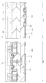
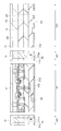
도 1은 휴대 전화기의 송수신부의 구성을 나타내는 블록도이다.
도 2는 실시 형태 1에 있어서의 전력 증폭기의 회로 블록을 나타낸 것이다.
도 3은 LDMOSFET의 단면 구조를 나타내는 단면도이다.
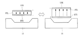
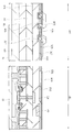
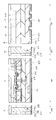
도 4는 박막 압전 벌크파 공진기의 모식적인 구성을 나타내는 도면이다.
도 5는 박막 압전 벌크파 공진기의 메커니즘을 설명하는 도면이다.
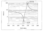
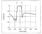
도 6은 박막 압전 벌크파 공진기의 주파수 특성을 나타내는 그래프이다.
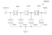
도 7은 송신 필터의 구성을 나타내는 도면이다.
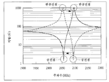
도 8은 안테나 단자와 송신 단자 사이에 직렬 접속된 박막 압전 벌크파 공진기의 주파수 특성과, 직렬 접속된 박막 압전 벌크파 공진기 각각의 노드와 접지의 사이에 접속된 박막 압전 벌크파 공진기의 주파수 특성을 나타내는 그래프이다.
도 9는 도 7에 도시한 송신 필터의 주파수 특성의 일례를 나타내는 그래프이다.
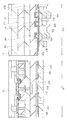
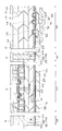
도 10은 FBAR형 공진기의 디바이스 구조를 나타내는 단면도이다.
도 11은 SMR형 공진기의 디바이스 구조를 나타내는 단면도이다.
도 12는 박막 압전 벌크파 공진기의 공진 주파수의 온도 특성을 나타내는 그래프이다.
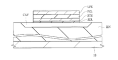
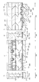
도 13은 실시 형태 1에 있어서의 반도체 장치의 구성을 나타내는 단면도이다.
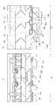
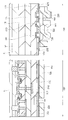
도 14는 실시 형태 1에 있어서의 반도체 장치의 제조 공정을 나타내는 단면도이다.
도 15는 도 14에 계속되는 반도체 장치의 제조 공정을 나타내는 단면도이다.
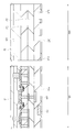
도 16은 도 15에 이어지는 반도체 장치의 제조 공정을 나타내는 단면도이다.
도 17은 도 16에 이어지는 반도체 장치의 제조 공정을 나타내는 단면도이다.
도 18은 도 17에 이어지는 반도체 장치의 제조 공정을 나타내는 단면도이다.
도 19는 도 18에 이어지는 반도체 장치의 제조 공정을 나타내는 단면도이다.
도 20은 도 19에 이어지는 반도체 장치의 제조 공정을 나타내는 단면도이다.
도 21은 도 20에 이어지는 반도체 장치의 제조 공정을 나타내는 단면도이다.
도 22는 도 21에 이어지는 반도체 장치의 제조 공정을 나타내는 단면도이다.
도 23은 도 22에 이어지는 반도체 장치의 제조 공정을 나타내는 단면도이다.
도 24는 실시 형태 2에 있어서의 반도체 장치의 구성을 나타내는 단면도이다.
도 25는 실시 형태 2에 있어서의 반도체 장치의 제조 공정을 나타내는 단면도이다.
도 26은 도 25에 이어지는 반도체 장치의 제조 공정을 나타내는 단면도이다.
도 27은 도 26에 이어지는 반도체 장치의 제조 공정을 나타내는 단면도이다.
도 28은 도 27에 이어지는 반도체 장치의 제조 공정을 나타내는 단면도이다.
도 29는 도 28에 이어지는 반도체 장치의 제조 공정을 나타내는 단면도이다.
도 30은 도 29에 이어지는 반도체 장치의 제조 공정을 나타내는 단면도이다.
도 31은 도 30에 이어지는 반도체 장치의 제조 공정을 나타내는 단면도이다.
도 32는 실시 형태 3에 있어서의 반도체 장치의 구성을 나타내는 단면도이다.
도 33은 실시 형태 3에 있어서의 반도체 장치의 변형예를 나타내는 단면도이다.
도 34는 실시 형태 3에 있어서의 반도체 장치의 제조 공정을 나타내는 단면도이다.
도 35는 도 34에 이어지는 반도체 장치의 제조 공정을 나타내는 단면도이다.
도 36은 도 35에 이어지는 반도체 장치의 제조 공정을 나타내는 단면도이다.
도 37은 도 36에 이어지는 반도체 장치의 제조 공정을 나타내는 단면도이다.
도 38은 도 37에 이어지는 반도체 장치의 제조 공정을 나타내는 단면도이다.
도 39는 도 38에 이어지는 반도체 장치의 제조 공정을 나타내는 단면도이다.
도 40은 도 39에 이어지는 반도체 장치의 제조 공정을 나타내는 단면도이다.
도 41은 도 40에 이어지는 반도체 장치의 제조 공정을 나타내는 단면도이다.
도 42는 도 41에 이어지는 반도체 장치의 제조 공정을 나타내는 단면도이다.
도 43은 도 42에 이어지는 반도체 장치의 제조 공정을 나타내는 단면도이다.
도 44는 실시 형태 4에 있어서의 반도체 장치의 구성을 나타내는 단면도이다.
도 45는 실시 형태 4에 있어서의 반도체 장치의 제조 공정을 나타내는 단면도이다.
도 46은 도 45에 이어지는 반도체 장치의 제조 공정을 나타내는 단면도이다.
도 47은 도 46에 이어지는 반도체 장치의 제조 공정을 나타내는 단면도이다.
도 48은 도 47에 이어지는 반도체 장치의 제조 공정을 나타내는 단면도이다.
도 49는 도 48에 이어지는 반도체 장치의 제조 공정을 나타내는 단면도이다.
도 50은 도 49에 이어지는 반도체 장치의 제조 공정을 나타내는 단면도이다.
도 51은 도 50에 이어지는 반도체 장치의 제조 공정을 나타내는 단면도이다.
도 52는 도 51에 이어지는 반도체 장치의 제조 공정을 나타내는 단면도이다.
도 53은 도 52에 이어지는 반도체 장치의 제조 공정을 나타내는 단면도이다.
도 54는 도 53에 이어지는 반도체 장치의 제조 공정을 나타내는 단면도이다.
도 55는 실시 형태 5에 있어서의 HBT의 디바이스 구조를 나타내는 단면도이다.
도 56은 실시 형태 5에 있어서의 반도체 장치의 구성을 나타내는 단면도이다.
도 57은 실시 형태 6에 있어서의 휴대 전화기의 송수신부의 구성을 나타내는 블록도이다.
도 58은 실시 형태 6에 있어서의 MOSFET의 디바이스 구조를 나타내는 단면도이다.
도 59는 실시 형태 6에 있어서의 반도체 장치의 구성을 나타내는 단면도이다.1 is a block diagram showing the configuration of a transceiver of a cellular phone.
Fig. 2 shows a circuit block of the power amplifier in the first embodiment.
3 is a cross-sectional view showing a cross-sectional structure of an LDMOSFET.
4 is a diagram illustrating a schematic configuration of a thin film piezoelectric bulk wave resonator.
5 is a diagram illustrating a mechanism of a thin film piezoelectric bulk wave resonator.
6 is a graph showing the frequency characteristics of a thin film piezoelectric bulk wave resonator.
7 is a diagram illustrating a configuration of a transmission filter.
8 shows frequency characteristics of a thin film piezoelectric bulk wave resonator connected in series between an antenna terminal and a transmitting terminal, and frequency characteristics of a thin film piezoelectric bulk wave resonator connected between a node and a ground of each of the thin film piezoelectric bulk wave resonators connected in series. It is a graph.
FIG. 9 is a graph showing an example of frequency characteristics of the transmission filter shown in FIG. 7.
Fig. 10 is a sectional view showing the device structure of an FBAR resonator.
Fig. 11 is a sectional view showing the device structure of an SMR resonator.
12 is a graph showing temperature characteristics of a resonance frequency of a thin film piezoelectric bulk wave resonator.
13 is a cross-sectional view showing the structure of a semiconductor device according to the first embodiment.
14 is a cross-sectional view illustrating the process of manufacturing the semiconductor device according to the first embodiment.
15 is a cross-sectional view illustrating the process of manufacturing the semiconductor device subsequent to FIG. 14.
16 is a cross-sectional view illustrating the process of manufacturing the semiconductor device subsequent to FIG. 15.
17 is a cross-sectional view illustrating the process of manufacturing the semiconductor device subsequent to FIG. 16.
18 is a cross-sectional view illustrating the process of manufacturing the semiconductor device subsequent to FIG. 17.
19 is a cross-sectional view illustrating the process of manufacturing the semiconductor device subsequent to FIG. 18.
20 is a cross-sectional view illustrating the process of manufacturing the semiconductor device subsequent to FIG. 19.
FIG. 21 is a cross-sectional view illustrating the process of manufacturing the semiconductor device subsequent to FIG. 20.
22 is a cross-sectional view illustrating the process of manufacturing the semiconductor device subsequent to FIG. 21.
FIG. 23 is a cross-sectional view illustrating the process of manufacturing the semiconductor device subsequent to FIG. 22.
24 is a cross-sectional view showing the configuration of a semiconductor device according to the second embodiment.
25 is a cross-sectional view illustrating the process of manufacturing the semiconductor device according to the second embodiment.
26 is a cross-sectional view illustrating the process of manufacturing the semiconductor device subsequent to FIG. 25.
27 is a cross-sectional view illustrating the process of manufacturing the semiconductor device subsequent to FIG. 26.
28 is a cross-sectional view illustrating the process of manufacturing the semiconductor device subsequent to FIG. 27.
29 is a cross-sectional view illustrating the process of manufacturing the semiconductor device subsequent to FIG. 28.
30 is a cross-sectional view illustrating the process of manufacturing the semiconductor device subsequent to FIG. 29.
31 is a cross-sectional view illustrating the process of manufacturing the semiconductor device subsequent to FIG. 30.
32 is a cross sectional view showing a configuration of a semiconductor device according to the third embodiment;
33 is a cross-sectional view showing a modification of the semiconductor device of
34 is a cross-sectional view illustrating the process of manufacturing the semiconductor device according to the third embodiment.
35 is a cross-sectional view illustrating the process of manufacturing the semiconductor device subsequent to FIG. 34.
36 is a cross-sectional view illustrating the process of manufacturing the semiconductor device subsequent to FIG. 35.
37 is a cross-sectional view illustrating the process of manufacturing the semiconductor device subsequent to FIG. 36.
38 is a cross-sectional view illustrating the process of manufacturing the semiconductor device subsequent to FIG. 37.
39 is a cross-sectional view illustrating the process of manufacturing the semiconductor device subsequent to FIG. 38.
40 is a cross-sectional view illustrating the process of manufacturing the semiconductor device subsequent to FIG. 39.
41 is a cross-sectional view illustrating the process of manufacturing the semiconductor device subsequent to FIG. 40.
42 is a cross-sectional view illustrating the process of manufacturing the semiconductor device subsequent to FIG. 41.
43 is a cross-sectional view illustrating the process of manufacturing the semiconductor device subsequent to FIG. 42.
44 is a cross-sectional view illustrating a configuration of a semiconductor device according to the fourth embodiment.
45 is a cross-sectional view illustrating the process of manufacturing the semiconductor device according to the fourth embodiment.
46 is a cross-sectional view illustrating the process of manufacturing the semiconductor device subsequent to FIG. 45.
47 is a cross-sectional view illustrating the process of manufacturing the semiconductor device subsequent to FIG. 46.
48 is a cross-sectional view illustrating the process of manufacturing the semiconductor device subsequent to FIG. 47.
49 is a cross-sectional view illustrating the process of manufacturing the semiconductor device subsequent to FIG. 48.
50 is a cross-sectional view illustrating the process of manufacturing the semiconductor device subsequent to FIG. 49.
51 is a cross-sectional view illustrating the process of manufacturing the semiconductor device subsequent to FIG. 50.
52 is a cross-sectional view illustrating the process of manufacturing the semiconductor device subsequent to FIG. 51.
53 is a cross-sectional view illustrating the process of manufacturing the semiconductor device subsequent to FIG. 52.
54 is a cross-sectional view illustrating the process of manufacturing the semiconductor device subsequent to FIG. 53.
FIG. 55 is a cross-sectional view showing the device structure of the HBT according to the fifth embodiment. FIG.
56 is a cross sectional view showing a configuration of a semiconductor device according to the fifth embodiment;
Fig. 57 is a block diagram showing the construction of a transmitter / receiver of the cellular phone according to the sixth embodiment.
Fig. 58 is a sectional view showing the device structure of the MOSFET in accordance with the sixth embodiment.
59 is a cross-sectional view showing the structure of a semiconductor device according to the sixth embodiment;
이하의 실시 형태에 있어서는 편의상 그 필요가 있을 때는, 복수의 섹션 또는 실시 형태로 분할하여 설명하지만, 특별히 명시한 경우를 제외하고, 그들은 서로 무관계한 것이 아니라, 한쪽은 다른 쪽의 일부 또는 전부의 변형예, 상세, 보충 설명 등의 관계에 있다.In the following embodiments, when necessary for the sake of convenience, the description is divided into a plurality of sections or embodiments, but unless specifically stated, they are not related to each other, and one side is a part or all modification of the other side. , Details, supplementary explanations, and so on.
또한, 이하의 실시 형태에 있어서, 요소의 수 등(개수, 수치, 양, 범위 등을 포함함)으로 언급하는 경우, 특별히 명시한 경우 및 원리적으로 명백하게 특정한 수로 한정되는 경우 등을 제외하고, 그 특정한 수로 한정되는 것이 아니라, 특정한 수 이상이어도 이하이어도 된다.In addition, in the following embodiments, when referring to the number (including the number, the numerical value, the amount, the range, etc.) of the elements, and the like, unless otherwise specified and in principle limited to a specific number, The number is not limited to a specific number, but may be more or less than a specific number.
또한, 이하의 실시 형태에 있어서, 그 구성 요소(요소 스텝 등도 포함함)는 특별히 명시한 경우 및 원리적으로 명백하게 필수적이라고 생각되는 경우 등을 제외하고, 반드시 필수적인 것이 아닌 것은 물론이다.It goes without saying that the constituent elements (including element steps and the like) in the following embodiments are not necessarily indispensable unless otherwise specified and in principle are apparently indispensable.
마찬가지로, 이하의 실시 형태에 있어서, 구성 요소 등의 형상, 위치 관계 등으로 언급할 때에는, 특별히 명시한 경우 및 원리적으로 명백하게 그렇지 않다고 생각되는 경우 등을 제외하고, 실질적으로 그 형상 등에 근사 또는 유사한 것 등을 포함하는 것으로 한다. 이것은, 상기 수치 및 범위에 대해서도 마찬가지이다.Likewise, in the following embodiments, when referring to the shape, positional relationship, and the like of constituent elements and the like, substantially similar or similar to the shape thereof, except for cases where it is specially specified and in principle, And the like. This also applies to the numerical value and the range.
또한, 실시 형태를 설명하기 위한 전체 도면에 있어서, 동일한 부재에는 원칙으로서 동일한 부호를 부여하고, 그 반복된 설명은 생략한다. 또한, 도면을 이해하기 쉽게 하기 위해 평면도이어도 해칭을 넣는 경우가 있다.In addition, in the whole figure for demonstrating embodiment, the same code | symbol is attached | subjected to the same member as a principle, and the repeated description is abbreviate | omitted. In order to facilitate understanding of the drawings, there is a case where a hatching is inserted even in a plan view.
(실시 형태 1)(Embodiment 1)
<휴대 전화기의 구성 및 동작><Configuration and operation of mobile phone>
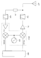
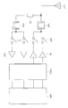
도 1은, 휴대 전화기의 송수신부의 구성을 나타내는 블록도이다. 도 1에 도시한 바와 같이, 휴대 전화기는 기저 대역부 BBU, 고주파 집적 회로부 RFICU, 전력 증폭기 PA, 송신 필터 TXF, 수신 필터 RXF, 이상기 PH 및 안테나 ANT를 갖고 있다.1 is a block diagram showing the configuration of a transceiver of a cellular phone. As shown in Fig. 1, the cellular phone has a baseband section BBU, a high frequency integrated circuit section RFICU, a power amplifier PA, a transmission filter TXF, a reception filter RXF, an ideal phase PH and an antenna ANT.
기저 대역부 BBU는, 송신 시에는 조작부를 통한 유저(통화자)로부터의 음성 신호(아날로그 신호)를 디지털 처리하여 기저 대역 신호를 생성할 수 있도록 구성되어 있다. 한편, 수신 시에는 디지털 신호인 기저 대역 신호로부터 음성 신호를 생성할 수 있도록 구성되어 있다.The baseband unit BBU is configured to digitally process an audio signal (analog signal) from a user (caller) through the operation unit to generate a baseband signal during transmission. On the other hand, when receiving, it is comprised so that a voice signal may be produced from the baseband signal which is a digital signal.
고주파 집적 회로부 RFICU는, 송신 시에는 기저 대역 신호를 변조하여 무선 주파수의 신호를 생성하고, 수신 시에는, 수신 신호를 복조하여 기저 대역 신호를 생성할 수 있도록 구성되어 있다. 구체적으로, 고주파 집적 회로부 RFICU는, 송신 믹서 TXMIX, 신시사이저(변조 신호원) SYN, 수신 믹서 RXMIX 및 저잡음 증폭기 LNA를 갖고 있다. 이때, 신시사이저 SYN은, 주파수가 안정된 수정 발진기 등의 기준 발진기를 사용하여 변조 신호를 얻도록 한 회로이며, 송신 믹서 TXMIX 및 수신 믹서 RXMIX는, 주파수를 변환하는 주파수 변환기이다. 또한, 저잡음 증폭기 LNA는, 노이즈의 증대를 억제하면서 미약한 수신 신호를 증폭하는 것이다.The high frequency integrated circuit unit RFICU is configured to generate a radio frequency signal by modulating the base band signal at the time of transmission, and to generate the base band signal at the reception by demodulating the received signal. Specifically, the high frequency integrated circuit unit RFICU has a transmission mixer TXMIX, a synthesizer (modulated signal source) SYN, a reception mixer RXMIX, and a low noise amplifier LNA. At this time, the synthesizer SYN is a circuit which obtains a modulated signal using a reference oscillator such as a crystal oscillator whose frequency is stable, and the transmit mixer TXMIX and the receive mixer RXMIX are frequency converters which convert frequencies. The low noise amplifier LNA amplifies a weak reception signal while suppressing an increase in noise.
전력 증폭기 PA는, 미약한 입력 신호와 서로 닮은 대전력의 신호를 전원으로부터 공급되는 전력으로 새롭게 생성하여 출력하는 회로이다. 안테나 ANT는, 전파를 송수신하기 위한 것이고, 송신 안테나와 수신 안테나를 겸하고 있다. 또한, 송신 필터 TXF는 송신 주파수 대역을 통과 대역으로 하고, 수신 주파수 대역을 저지 대역으로 하는 대역 통과 필터이며, 수신 필터 RXF는 수신 주파수 대역을 통과 대역으로 하고, 송신 주파수 대역을 저지 대역으로 하는 대역 통과 필터이다. 그리고, 이상기 PH는 임피던스를 제어하기 위해 설치되어 있다.The power amplifier PA is a circuit for newly generating and outputting a large power signal similar to the weak input signal with power supplied from a power source. The antenna ANT is for transmitting and receiving radio waves, and also serves as a transmitting antenna and a receiving antenna. The transmission filter TXF is a band pass filter in which the transmission frequency band is the pass band and the reception frequency band is the stop band, and the reception filter RXF is the band in which the reception frequency band is the pass band and the transmission frequency band is the stop band. It is a pass filter. The abnormal phase PH is provided for controlling the impedance.
예를 들어, 휴대 전화기와 같이 송신과 수신을 동시에 행하는 무선기에 있어서, 송신 안테나와 수신 안테나를 하나의 안테나로 공용한 경우, 큰 전력의 송신 신호가 수신부에 유입하고, 휴대 전화기에서의 수신 신호의 수신을 방해할 우려가 발생한다. 따라서, 휴대 전화기에 있어서는, 송신 경로와 수신 경로를 전기적으로 분리하기 위해서, 휴대 전화기에는, 송신 필터 TXF와 수신 필터 RXF가 설치되어 있다. 즉, 송신 경로에 송신 필터 TXF를 설치함으로써, 송신 경로에는, 송신 주파수 대역의 송신 신호만이 전달하게 되는 한편, 수신 경로에 수신 필터 RXF를 설치함으로써, 수신 경로에는, 수신 주파수 대역의 수신 신호만이 전달하게 된다. 이 결과, 수신 경로에 유입하려고 하는 송신 신호는, 수신 필터 RXF에 의해 차단되고, 수신 경로에 송신 신호가 유입되는 것을 억제할 수 있다.For example, in a wireless device that simultaneously transmits and receives like a mobile phone, when a transmitting antenna and a receiving antenna are shared by one antenna, a large power transmission signal flows into the receiving unit, and There is a fear of disturbing reception. Therefore, in the mobile telephone, the transmission telephone TXF and the reception filter RXF are provided in the portable telephone in order to electrically separate the transmission path and the reception path. That is, by providing the transmission filter TXF in the transmission path, only the transmission signal of the transmission frequency band is transmitted to the transmission path, while providing the reception filter RXF in the reception path, and only the reception signal of the reception frequency band is provided in the reception path. This will pass. As a result, the transmission signal which tries to flow into a reception path is interrupted | blocked by the reception filter RXF, and it can suppress that a transmission signal flows into a reception path.
또한, 송신 필터 TXF와 수신 필터 RXF의 사이에 이상기 PH가 설치되어 있다. 이 이상기 PH는, 저지 대역의 임피던스를 고임피던스로 하기 위해 설치되어 있으며, 통과 대역의 임피던스에 대하여 저지 대역의 임피던스를 충분히 높은 임피던스로 함으로써, 송신 필터 TXF와 수신 필터 RXF를 접속한 경우의 영향을 작게 할 수 있다.The abnormal phase PH is provided between the transmission filter TXF and the reception filter RXF. This abnormal phase PH is provided to make the impedance of the stop band high impedance, and by making the impedance of the stop band sufficiently high with respect to the impedance of the pass band, the effect of connecting the transmission filter TXF and the reception filter RXF is affected. It can be made small.
휴대 전화기는, 상기와 같이 구성되어 있으며, 이하에, 그 동작에 대하여 간단히 설명한다. 우선, 송신 신호를 송신하는 경우에 대하여 설명한다. 기저 대역부 BBU에서 음성 신호 등의 아날로그 신호를 디지털 처리함으로써 생성된 기저 대역 신호는, 고주파 집적 회로부 RFICU에 입력한다. 고주파 집적 회로부 RFICU에서는, 입력한 기저 대역 신호를, 신시사이저(변조 신호원) SYN 및 송신 믹서 TXMIX에 의해, 무선 주파수(RF(Radio Frequency) 주파수)의 송신 신호로 변환한다. 무선 주파수로 변환된 송신 신호는, 고주파 집적 회로부 RFICU로부터 전력 증폭기(PA 모듈) PA로 출력된다. 전력 증폭기 PA에 입력한 무선 주파수의 송신 신호는, 전력 증폭기 PA에 의해 증폭된 후, 송신 필터 TXF를 통해 안테나 ANT로부터 송신된다.The mobile telephone is configured as described above, and the operation thereof will be briefly described below. First, a case of transmitting a transmission signal will be described. The baseband signal generated by digitally processing analog signals such as voice signals in the baseband section BBU is input to the high frequency integrated circuit section RFICU. In the high frequency integrated circuit unit RFICU, the input baseband signal is converted into a transmission signal of radio frequency (RF frequency) by a synthesizer (modulated signal source) SYN and a transmission mixer TXMIX. The transmission signal converted into the radio frequency is output from the high frequency integrated circuit unit RFICU to the power amplifier (PA module) PA. The transmission signal of the radio frequency input to the power amplifier PA is amplified by the power amplifier PA, and then transmitted from the antenna ANT through the transmission filter TXF.
다음으로, 수신 신호를 수신하는 경우에 대하여 설명한다. 안테나 ANT에 의해 수신된 무선 주파수의 수신 신호는, 수신 필터 RXF를 통과한 후, 고주파 집적 회로부 RFICU에 입력한다. 고주파 집적 회로부 RFICU에서는, 우선 저잡음 증폭기 LNA에 의해 입력한 수신 신호를 증폭한 후, 신시사이저(변조 신호원) SYN 및 수신 믹서 RXMIX에 의해 주파수 변환을 행한다. 그리고, 주파수 변환된 수신 신호의 검파가 행해지고, 기저 대역 신호가 추출된다. 그 후, 이 기저 대역 신호는, 고주파 집적 회로부 RFICU로부터 기저 대역부 BBU로 출력된다. 이 기저 대역 신호가 기저 대역부 BBU에서 처리되고, 음성 신호가 출력된다.Next, a case of receiving a received signal will be described. The reception signal of the radio frequency received by the antenna ANT passes through the reception filter RXF, and is then input to the high frequency integrated circuit unit RFICU. In the RFICU of the high frequency integrated circuit, first, a received signal input by the low noise amplifier LNA is amplified, and then frequency conversion is performed by a synthesizer (modulated signal source) SYN and a receive mixer RXMIX. Then, the frequency-converted received signal is detected, and the baseband signal is extracted. This baseband signal is then output from the high frequency integrated circuit unit RFICU to the baseband unit BBU. This baseband signal is processed in the baseband section BBU, and an audio signal is output.
<전력 증폭기(PA 모듈)의 구성><Configuration of Power Amplifier (PA Module)>
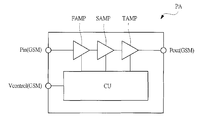
전술한 바와 같이, 휴대 전화기로부터 신호를 송신할 때, 전력 증폭기 PA에 의해 송신 신호는 증폭된다. 이하에서는, 이 전력 증폭기 PA의 구성에 대하여 설명한다.As described above, when transmitting a signal from the cellular phone, the transmission signal is amplified by the power amplifier PA. Hereinafter, the configuration of this power amplifier PA will be described.
도 2는, 본 실시 형태 1에 있어서의 전력 증폭기 PA의 회로 블록을 나타낸 것이다. 도 2를 참조하면서, 전력 증폭기 PA의 회로 블록에 대하여 설명한다. 도 2에 있어서, 전력 증폭기 PA는 제어 회로 CU, 증폭부 FAMP, 증폭부 SAMP 및 증폭부 TAMP를 갖고 있다. 이 전력 증폭기 PA는, 예를 들어 제1 주파수를 이용한 GSM(Global System for Mobile Communication) 방식에 사용되는 것이며, 주파수 대역으로서 880㎒ 내지 915㎒를 사용하고 있는 신호를 증폭할 수 있도록 되어 있다.2 shows a circuit block of the power amplifier PA according to the first embodiment. With reference to FIG. 2, the circuit block of the power amplifier PA is demonstrated. In FIG. 2, the power amplifier PA has a control circuit CU, an amplifier part FAMP, an amplifier part SAMP, and an amplifier part TAMP. This power amplifier PA is used for the GSM (Global System for Mobile Communication) system using a 1st frequency, for example, and can amplify the signal using 880 MHz-915 MHz as a frequency band.
전술한 전력 증폭기 PA에 있는 제어 회로 CU는, 제어 신호를 입력하고, 입력한 제어 신호에 기초하여 증폭부 FAMP, 증폭부 SAMP 및 증폭부 TAMP의 각 증폭부를 제어하도록 구성되어 있다. 이 제어 회로 CU는 증폭부 FAMP, 증폭부 SAMP 및 증폭부 TAMP를 제어하는 제어 신호 Vcontrol(GSM)을 입력할 수 있도록 되어 있으며, 증폭부 FAMP, 증폭부 SAMP 및 증폭부 TAMP는, 제어 신호 Vcontrol(GSM)에 기초하여 제어되도록 되어 있다. 이와 같이 하여, 본 실시 형태 1의 전력 증폭기 PA는, GSM 방식에 있어서의 송신 신호의 증폭을 제어하고 있다. 제어 회로 CU는, 예를 들어 MOSFET(Metal Oxide Semiconductor Field Effect Transistor) 등으로 구성되어 있다.The control circuit CU in the above-described power amplifier PA is configured to input a control signal and to control the respective amplification sections of the amplifying section FAMP, the amplifying section SAMP, and the amplifying section TAMP based on the input control signal. The control circuit CU is capable of inputting a control signal Vcontrol (GSM) for controlling the amplification section FAMP, the amplification section SAMP, and the amplifying section TAMP. The amplifying section FAMP, the amplifying section SAMP, and the amplifying section TAMP is a control signal Vcontrol ( Control based on GSM). In this manner, the power amplifier PA of the first embodiment controls amplification of the transmission signal in the GSM system. The control circuit CU is composed of, for example, a MOSFET (Metal Oxide Semiconductor Field Effect Transistor).
계속해서, 증폭부 FAMP, 증폭부 SAMP 및 증폭부 TAMP는, GSM 방식의 입력 전력(입력 신호) Pin(GSM)을 입력하고, 이 입력 전력 Pin(GSM)을 3단계에 걸쳐 증폭하도록 구성되어 있다. 즉, 입력 전력 Pin(GSM)을 우선 증폭부 FAMP에 의해 증폭한 후, 증폭부 FAMP에 의해 증폭한 전력을 증폭부 SAMP에 의해 증폭한다. 그리고, 증폭부 SAMP에 의해 증폭한 전력은, 종단의 증폭부 TAMP에 의해 증폭된 후, 전력 증폭기 PA로부터 출력 신호 Pout(GSM)로서 출력된다. 이와 같이, 증폭부 FAMP, 증폭부 SAMP 및 증폭부 TAMP에서는, GSM 방식에 의한 전력을 증폭할 수 있도록 되어 있다. 이들 증폭부 FAMP, 증폭부 SAMP 및 증폭부 TAMP는, 예를 들어LDMOSFET(Laterally Diffused Metal Oxide Semiconductor Field Effect Transistor)으로 형성되어 있다.Subsequently, the amplifying unit FAMP, the amplifying unit SAMP, and the amplifying unit TAMP are configured to input a GSM type input power (input signal) Pin (GSM) and amplify the input power Pin (GSM) in three stages. . That is, the input power Pin (GSM) is first amplified by the amplifier FAMP, and then the power amplified by the amplifier FAMP is amplified by the amplifier SAMP. The power amplified by the amplifier SAMP is amplified by the terminal amplifier TAMP at the end and then output as an output signal Pout (GSM) from the power amplifier PA. In this way, the amplifying section FAMP, the amplifying section SAMP, and the amplifying section TAMP can amplify the power by the GSM system. These amplification part FAMP, amplification part SAMP, and amplification part TAMP are formed with LDMOSFET (Laterally Diffused Metal Oxide Semiconductor Field Effect Transistor), for example.
<LDMOSFET의 디바이스 구조><LDMOSFET device structure>
다음으로, 전력 증폭기 PA의 증폭부 FAMP, 증폭부 SAMP 및 증폭부 TAMP를 구성하는 LDMOSFET의 디바이스 구조에 대하여 도면을 참조하면서 설명한다.Next, the device structure of the LDMOSFET constituting the amplifier FAMP, amplifier SAMP, and amplifier TAMP of the power amplifier PA will be described with reference to the drawings.
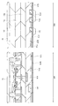
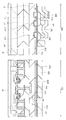
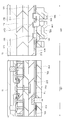
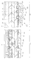
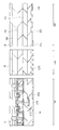
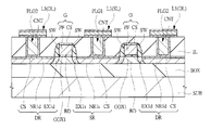
도 3은, LDMOSFET의 단면 구조를 나타내는 단면도이다. 도 3에 있어서, p+형 실리콘 단결정으로 이루어지는 반도체 기판(1S) 위에는, p-형 반도체층으로 이루어지는 에피택셜층 EPI가 형성되어 있다. 그리고, 반도체 기판(1S)에는, 홈 DT가 형성되어 있으며, 이 홈 DT에는, 예를 들어 p형 폴리실리콘막이 매립되어 p형 펀칭층 PL이 형성되어 있다. 또한, 반도체 기판(1S)의 표면에는, p형 웰 PWL이 형성되어 있다.3 is a cross-sectional view showing the cross-sectional structure of an LDMOSFET. In Fig. 3, the epitaxial layer EPI made of the p − type semiconductor layer is formed on the
다음으로, 반도체 기판(1S)의 표면에는, 게이트 절연막 GOX가 형성되어 있고, 이 게이트 절연막 GOX 위에 게이트 전극 G 및 캡 절연막 CAP가 형성되어 있다. 게이트 절연막 GOX는, 예를 들어 얇은 산화실리콘막 등으로 이루어지고, 게이트 전극 G는 폴리실리콘막으로 형성되어 있다. 그리고, 게이트 전극 G에 정합하여, n-형 오프셋 드레인 영역 ODR1이 형성됨과 함께, n-형 소스 영역 SR1이 형성되어 있다. n-형 소스 영역 SR1에 인접하도록 p형 할로 영역 HALO가 형성되어 있다.Next, a gate insulating film GOX is formed on the surface of the
게이트 전극 G의 양측 측벽에는, 사이드 월 SW가 형성되어 있으며, 이 사이드 월 SW에 정합하여, n형 오프셋 드레인 영역 ODR2 및 n+형 드레인 영역 DR이 형성되어 있다. 마찬가지로, n-형 소스 영역 SR1의 외측에는, 사이드 월 SW에 정합하여, n+형 소스 영역 SR2가 형성되어 있다. 그리고, n+형 소스 영역 SR2의 외측에 p+형 반도체 영역 PR1이 형성되어 있다.Sidewalls SW are formed on both sidewalls of the gate electrode G, and the n-type offset drain region ODR2 and the n + -type drain region DR are formed in accordance with the sidewall SW. Similarly, n + type source region SR2 is formed outside the n − type source region SR1 in accordance with the sidewall SW. The p + type semiconductor region PR1 is formed outside the n + type source region SR2.
이와 같이 구성된 LDMOSFET 위에는, 질화실리콘막 SN 및 산화실리콘막의 적층막으로 이루어지는 층간 절연막 IL1이 형성되어 있으며, 이 층간 절연막 IL1을 관통하는 콘택트 홀 CNT1이 형성되어 있다. 콘택트 홀 CNT1에는, 예를 들어 배리어막이 텅스텐막으로 이루어지는 플러그 PLG1이 매립되어 있다.On the LDMOSFET configured as described above, an interlayer insulating film IL1 made of a laminated film of silicon nitride film SN and a silicon oxide film is formed, and a contact hole CNT1 penetrating the interlayer insulating film IL1 is formed. In the contact hole CNT1, for example, plug PLG1 having a barrier film made of a tungsten film is embedded.
플러그 PLG1을 형성한 층간 절연막 IL1 위에는, 예를 들어 알루미늄막으로 이루어지는 제1층 배선 L1이 형성되고, 이 제1층 배선 L1을 덮도록 산화실리콘막으로 이루어지는 층간 절연막 IL2가 형성되어 있다. 이 층간 절연막 IL2에는, 제1층 배선 L1로 관통하는 접속 구멍 CNT2가 형성되어 있으며, 이 접속 구멍 CNT2에 플러그 PLG2가 매립되어 있다. 그리고, 플러그 PLG2를 형성한 층간 절연막 IL2 위에는, 제2층 배선 L2가 형성되어 있다. 이 제2층 배선 L2보다 상층에는, 필요에 따라서 다른 배선층이나 층간 절연막이 형성되지만, 도 3에서는 생략한다. 또한, 도 3에 도시한 LDMOSFET이 복수개 병렬로 접속되고, 예를 들어 도 2에 도시한 증폭부 FAMP, 증폭부 SAMP 및 증폭부 TAMP가 형성된다.On the interlayer insulation film IL1 in which the plug PLG1 was formed, the 1st layer wiring L1 which consists of aluminum films, for example is formed, and the interlayer insulation film IL2 which consists of a silicon oxide film is formed so that this 1st layer wiring L1 may be covered. Connection hole CNT2 which penetrates into 1st layer wiring L1 is formed in this interlayer insulation film IL2, and plug PLG2 is embedded in this connection hole CNT2. The second layer wiring L2 is formed on the interlayer insulating film IL2 on which the plug PLG2 is formed. Although another wiring layer and an interlayer insulation film are formed in this layer above this 2nd layer wiring L2 as needed, it abbreviate | omits in FIG. In addition, a plurality of LDMOSFETs shown in FIG. 3 are connected in parallel, for example, an amplifier part FAMP, an amplifier part SAMP, and an amplifier part TAMP shown in FIG. 2 are formed.
<송신 필터 및 수신 필터의 구성><Configuration of Send and Receive Filters>
계속해서, 송신 필터 및 수신 필터의 구성에 대하여 설명한다. 본 실시 형태 1에서는, 도 1에 도시한 송신 필터 TXF 및 수신 필터 RXF를 박막 압전 벌크파 공진기로 구성하고 있다. 이하에, 이 박막 압전 벌크파 공진기에 대하여 설명한다.Next, the configuration of the transmission filter and the reception filter will be described. In the first embodiment, the transmission filter TXF and the reception filter RXF shown in FIG. 1 are constituted by a thin film piezoelectric bulk wave resonator. The thin film piezoelectric bulk wave resonator will be described below.
도 4는, 박막 압전 벌크파 공진기의 모식적인 구성을 나타내는 도면이다. 도 4에 있어서, 박막 압전 벌크파 공진기는, 예를 들어 박막 형성 장치로 형성한 압전층 PZL과, 이 압전층 PZL을 사이에 끼우도록 존재하는 상부 전극 UPE 및 하부 전극 BTE를 갖고 있다. 이때, 예를 들어 압전층 PZL은, 질화알루미늄(AlN)막으로 구성되고, 상부 전극 UPE 및 하부 전극 BTE는, 몰리브덴(Mo)막으로 구성된다.4 is a diagram illustrating a schematic configuration of a thin film piezoelectric bulk wave resonator. In FIG. 4, the thin film piezoelectric bulk wave resonator has, for example, a piezoelectric layer PZL formed by a thin film forming apparatus, and an upper electrode UPE and a lower electrode BTE present to sandwich the piezoelectric layer PZL. At this time, for example, the piezoelectric layer PZL is made of an aluminum nitride (AlN) film, and the upper electrode UPE and the lower electrode BTE are made of a molybdenum (Mo) film.
여기서, 압전층 PZL은, 두께 방향으로 분극하고 있으며, 상부 전극 UPE와 하부 전극 BTE의 사이에 인가되는 교류 전압에 의해, 압전층 PZL의 분극 방향이 변화한다. 예를 들어, 도 5에 도시한 바와 같이, 반도체 기판(1S) 위에 설치된 박막 압전 벌크파 공진기에 있어서, 상부 전극 UPE에 정전위가 인가되고, 하부 전극 BTE에 부전위가 인가되면, 압전층 PZL의 분극 방향은 하향으로 된다. 한편, 상부 전극 UPE에 부전위가 인가되고, 하부 전극 BTE에 정전위가 인가되면, 압전층 PZL의 분극 방향은 상향으로 된다. 이와 같이 압전층 PZL의 분극 방향은 상부 전극 UPE와 하부 전극 BTE에 인가되는 전압의 극성에 따라 변화한다. 따라서, 상부 전극 UPE와 하부 전극 BTE의 사이에 교류 전압을 인가하면, 압전층 PZL의 분극 방향이 상하 방향으로 변화하게 된다.Here, the piezoelectric layer PZL is polarized in the thickness direction, and the polarization direction of the piezoelectric layer PZL changes with the alternating voltage applied between the upper electrode UPE and the lower electrode BTE. For example, as shown in FIG. 5, in the thin film piezoelectric bulk wave resonator provided on the
이때, 압전층 PZL은, 분극 방향에 의해 압전층 PZL의 두께가 변화한다는 특징이 있다. 즉, 상부 전극 UPE와 하부 전극 BTE의 사이에 교류 전압을 인가하면, 압전층 PZL의 분극 방향이 변화하고, 이에 의해, 압전층 PZL의 두께 방향의 막 두께가 변화한다. 이것은, 상부 전극 UPE와 하부 전극 BTE의 사이에 교류 전압이 인가되면, 압전층 PZL의 분극 방향이 상하 반전하는 결과, 압전층 PZL이 두께 방향으로 신축하고, 이 압전층 PZL의 두께 방향의 신축에 의해 탄성파가 발생하는 것을 의미하고 있다. 박막 압전 벌크파 공진기에서는, 이 탄성파에 의한 공진 진동을 이용하고 있다.At this time, the piezoelectric layer PZL is characterized in that the thickness of the piezoelectric layer PZL changes depending on the polarization direction. That is, when an alternating voltage is applied between the upper electrode UPE and the lower electrode BTE, the polarization direction of the piezoelectric layer PZL is changed, whereby the film thickness in the thickness direction of the piezoelectric layer PZL is changed. This is because when the alternating voltage is applied between the upper electrode UPE and the lower electrode BTE, the polarization direction of the piezoelectric layer PZL is reversed up and down, so that the piezoelectric layer PZL is stretched in the thickness direction and stretched in the thickness direction of the piezoelectric layer PZL. This means that an acoustic wave is generated. In the thin film piezoelectric bulk wave resonator, the resonance vibration caused by the elastic wave is used.
구체적으로, 박막 압전 벌크파 공진기의 주파수 특성의 일례에 대하여 설명한다. 도 6은, 박막 압전 벌크파 공진기의 주파수 특성을 나타내는 그래프이다. 도 6에 있어서, 횡축은 주파수(㎒)를 나타내고 있으며, 종축은 저항(Ω)(임피던스)을 나타내고 있다. 도 6에 도시한 바와 같이, 박막 압전 벌크파 공진기에서는, 예를 들어 2060㎒ 부근에 공진점이 존재하고, 2090㎒ 부근에 반공진점이 존재하는 것을 알 수 있다. 이 도 6에 도시한 바와 같이, 박막 압전 벌크파 공진기에서는, 공진점 근방에서 저항이 현저하게 저하하는 한편, 반공진점 근방에서 저항이 현저하게 커지는 것을 알 수 있다. 이것은, 박막 압전 벌크파 공진기에 있어서, 공진점 부근에서의 저항이 작아지기 때문에, 공진점 부근의 주파수 진동은 박막 압전 벌크파 공진기를 통과하기 쉬워지는 한편, 반공진점 부근에서의 저항이 커지는 점에서, 반공진점 부근의 주파수 진동은 박막 압전 벌크파 공진기에서 감쇠하여 통과하기 어려워짐을 의미하고 있다. 즉, 박막 압전 벌크파 공진기에서는, 공진점 부근의 주파수 진동을 통과시키는 한편, 반공진점 부근의 주파수 진동을 차단한다고 하는 필터 특성을 갖고 있는 것을 알 수 있다. 따라서, 박막 압전 벌크파 공진기는, 대역 통과 필터인 송신 필터 TXF 또는 수신 필터 RXF에 사용할 수 있는 것을 알 수 있다.Specifically, an example of the frequency characteristics of the thin film piezoelectric bulk wave resonator will be described. 6 is a graph showing the frequency characteristics of a thin film piezoelectric bulk wave resonator. In FIG. 6, the horizontal axis represents frequency (MHz), and the vertical axis represents resistance (Ω) (impedance). As shown in FIG. 6, in the thin film piezoelectric bulk wave resonator, for example, a resonance point exists near 2060 MHz and an anti-resonance point exists near 2090 MHz. As shown in Fig. 6, in the thin film piezoelectric bulk wave resonator, the resistance is remarkably decreased near the resonance point, and the resistance is remarkably large near the anti-resonance point. This is because, in the thin film piezoelectric bulk wave resonator, the resistance near the resonance point becomes small, so that the frequency vibration near the resonance point tends to pass through the thin film piezoelectric bulk wave resonator, while the resistance near the anti-resonant point increases. The frequency oscillation near the resonance point means that the thin film piezoelectric bulk wave resonator becomes difficult to pass through. In other words, it can be seen that the thin film piezoelectric bulk wave resonator has a filter characteristic of passing frequency vibration near the resonance point and blocking frequency vibration near the anti-resonance point. Therefore, it turns out that a thin film piezoelectric bulk wave resonator can be used for the transmission filter TXF or the reception filter RXF which is a bandpass filter.
이하에서는, 전술한 박막 압전 벌크파 공진기를 이용한 송신 필터 TXF 또는 수신 필터 RXF의 구성에 대하여 설명한다. 또한, 송신 필터 TXF와 수신 필터 RXF의 구성은 거의 마찬가지이기 때문에, 송신 필터 TXF를 예로 들어 설명한다.Hereinafter, the configuration of the transmission filter TXF or the reception filter RXF using the thin film piezoelectric bulk wave resonator described above will be described. In addition, since the structure of the transmission filter TXF and the reception filter RXF is substantially the same, it demonstrates using transmission filter TXF as an example.
도 7은, 송신 필터 TXF의 구성을 나타내는 도면이다. 도 7에 도시한 바와 같이, 송신 필터 TXF는, 안테나 단자 ANT(OUT)와 송신 단자 TX의 사이에 설치되어 있다. 구체적으로, 송신 필터 TXF는, 안테나 단자 ANT(OUT)와 송신 단자 TX의 사이에 직렬 접속된 3개의 박막 압전 벌크파 공진기 BAW1 내지 BAW3과, 3개의 박막 압전 벌크파 공진기 BAW1 내지 BAW3 각각의 노드와 접지(GND)의 사이에 접속된 4개의 박막 압전 벌크파 공진기 BAW4 내지 BAW7로 구성되어 있다. 이와 같이 송신 필터 TXF에 있어서, 안테나 단자 ANT(OUT)와 송신 단자 TX의 사이에 직렬 접속된 박막 압전 벌크파 공진기 BAW1 내지 BAW3과, 박막 압전 벌크파 공진기 BAW1 내지 BAW3 각각의 노드와 접지(GND)의 사이에 접속된 박막 압전 벌크파 공진기 BAW4 내지 BAW7을 설치하는 이유에 대하여 설명한다.7 is a diagram illustrating a configuration of the transmission filter TXF. As shown in Fig. 7, the transmission filter TXF is provided between the antenna terminal ANT (OUT) and the transmission terminal TX. Specifically, the transmission filter TXF includes three thin film piezoelectric bulk wave resonators BAW1 to BAW3 and three nodes of the three thin film piezoelectric bulk wave resonators BAW1 to BAW3 connected in series between the antenna terminal ANT (OUT) and the transmission terminal TX. It consists of four thin film piezoelectric bulk wave resonators BAW4 to BAW7 connected between ground GND. Thus, in the transmission filter TXF, the nodes and ground (GND) of the thin film piezoelectric bulk wave resonators BAW1 to BAW3 and the thin film piezoelectric bulk wave resonators BAW1 to BAW3 respectively connected in series between the antenna terminal ANT (OUT) and the transmission terminal TX. The reason for providing the thin film piezoelectric bulk wave resonators BAW4 to BAW7 connected between them will be described.
도 8은, 안테나 단자 ANT(OUT)와 송신 단자 TX의 사이에 직렬 접속된 박막 압전 벌크파 공진기 BAW1 내지 BAW3의 주파수 특성과, 박막 압전 벌크파 공진기 BAW1 내지 BAW3 각각의 노드와 접지(GND)의 사이에 접속된 박막 압전 벌크파 공진기 BAW4 내지 BAW7의 주파수 특성을 나타내는 그래프이다. 도 8에 있어서, 횡축은 주파수(㎒)를 나타내고 있으며, 종축은 저항(Ω)(임피던스)을 나타내고 있다.Fig. 8 shows the frequency characteristics of the thin film piezoelectric bulk wave resonators BAW1 to BAW3 connected in series between the antenna terminal ANT (OUT) and the transmission terminal TX, and the nodes of the thin film piezoelectric bulk wave resonators BAW1 to BAW3 and ground (GND). It is a graph showing the frequency characteristics of the thin film piezoelectric bulk wave resonators BAW4 to BAW7 connected therebetween. In FIG. 8, the horizontal axis represents frequency (MHz), and the vertical axis represents resistance (Ω) (impedance).
우선, 도 8에 있어서, 예를 들어 실선으로 나타내는 곡선이 안테나 단자 ANT(OUT)과 송신 단자 TX의 사이에 직렬 접속된 박막 압전 벌크파 공진기 BAW1 내지 BAW3의 주파수 특성을 나타내고 있으며, 파선으로 나타내는 곡선이 박막 압전 벌크파 공진기 BAW1 내지 BAW3 각각의 노드와 접지(GND)의 사이에 접속된 박막 압전 벌크파 공진기 BAW4 내지 BAW7의 주파수 특성을 나타내고 있다. 이때, 도 8에 도시한 바와 같이, 실선으로 나타내는 곡선의 공진점에 대응하는 주파수에 파선으로 나타내는 곡선의 반공진점이 존재하고, 실선으로 나타내는 곡선의 반공진점에 대응하는 주파수에 파선으로 나타내는 곡선의 공진점이 존재하고 있는 것을 알 수 있다. 즉, 안테나 단자 ANT(OUT)와 송신 단자 TX의 사이에 직렬 접속된 박막 압전 벌크파 공진기 BAW1 내지 BAW3의 주파수 특성(실선)과, 박막 압전 벌크파 공진기 BAW1 내지 BAW3 각각의 노드와 접지(GND)의 사이에 접속된 박막 압전 벌크파 공진기 BAW4 내지 BAW7의 주파수 특성(파선)이 반대로 되어 있는 것을 알 수 있다. 이것은, 박막 압전 벌크파 공진기 BAW1 내지 BAW3이 안테나 단자 ANT(OUT)와 송신 단자TX의 사이에 직렬 접속되어 있는 것에 반하여, 박막 압전 벌크파 공진기 BAW4 내지 BAW7이 박막 압전 벌크파 공진기 BAW1 내지 BAW3 각각의 노드와 접지(GND)의 사이에 접속되어 있는 것에 기인한다. 즉, 도 8에 도시한 바와 같이, 박막 압전 벌크파 공진기의 접속 위치를 바꿈으로써, 박막 압전 벌크파 공진기의 주파수 특성을 바꿀 수 있는 것이다.First, in FIG. 8, for example, a curve indicated by a solid line shows the frequency characteristics of the thin film piezoelectric bulk wave resonators BAW1 to BAW3 connected in series between the antenna terminal ANT (OUT) and the transmission terminal TX, and is indicated by a broken line. Frequency characteristics of the thin film piezoelectric bulk wave resonators BAW4 to BAW7 connected between the nodes of the thin film piezoelectric bulk wave resonators BAW1 to BAW3 and ground GND are shown. At this time, as shown in Fig. 8, the resonance point of the curve represented by the broken line is present at the frequency corresponding to the resonance point of the curve indicated by the solid line, and the anti-resonance point of the curve represented by the broken line is shown at the frequency corresponding to the anti-resonance point of the curve represented by the solid line. It can be seen that this exists. That is, the frequency characteristics (solid line) of the thin film piezoelectric bulk wave resonators BAW1 to BAW3 connected in series between the antenna terminal ANT (OUT) and the transmission terminal TX, and the node and ground (GND) of each of the thin film piezoelectric bulk wave resonators BAW1 to BAW3. It can be seen that the frequency characteristics (dashed lines) of the thin film piezoelectric bulk wave resonators BAW4 to BAW7 connected in the opposite direction are reversed. This is because the thin film piezoelectric bulk wave resonators BAW1 to BAW3 are connected in series between the antenna terminal ANT (OUT) and the transmission terminal TX, whereas the thin film piezoelectric bulk wave resonators BAW4 to BAW7 are each of the thin film piezoelectric bulk wave resonators BAW1 to BAW3. This is due to the connection between the node and ground (GND). That is, as shown in FIG. 8, the frequency characteristic of a thin film piezoelectric bulk wave resonator can be changed by changing the connection position of a thin film piezoelectric bulk wave resonator.
그리고, 나아가 박막 압전 벌크파 공진기를 구성하는 압전층 PZL과 상부 전극 UPE와 하부 전극 BTE의 총 막 두께를 바꿈으로써(실제로는, 상부 전극 UPE의 일부 위에 설치한 션트 전극의 막 두께를 바꾸는 경우가 많음), 공진점을 변화시킬 수 있다. 따라서, 예를 들어 박막 압전 벌크파 공진기 BAW1 내지 BAW3을 구성하는 압전층 PZL과 상부 전극 UPE와 하부 전극 BTE의 총 막 두께와, 박막 압전 벌크파 공진기 BAW4 내지 BAW7을 구성하는 압전층 PZL과 상부 전극 UPE와 하부 전극 BTE의 총 막 두께를 바꿈으로써, 도 8의 실선으로 나타내는 곡선의 공진점과, 파선으로 나타내는 곡선의 공진점의 간격을 임의로 조정할 수 있다. 이 결과, 도 7에 도시한 송신 필터 TXF의 주파수 특성은, 도 8의 실선으로 나타내는 곡선과 파선으로 나타내는 곡선의 총합으로 되기 때문에, 예를 들어 도 9에 도시한 바와 같은 주파수 특성으로 된다.Further, by changing the total film thickness of the piezoelectric layer PZL, the upper electrode UPE, and the lower electrode BTE constituting the thin film piezoelectric bulk wave resonator (actually, the film thickness of the shunt electrode provided on a part of the upper electrode UPE may be changed). Many), the resonance point can be changed. Thus, for example, the total film thickness of the piezoelectric layer PZL constituting the thin film piezoelectric bulk wave resonators BAW1 to BAW3, the upper electrode UPE and the lower electrode BTE, and the piezoelectric layer PZL and the upper electrode constituting the thin film piezoelectric bulk wave resonators BAW4 to BAW7. By changing the total film thickness of the UPE and the lower electrode BTE, the interval between the resonance point of the curve shown by the solid line of FIG. 8 and the resonance point of the curve shown by the broken line can be arbitrarily adjusted. As a result, since the frequency characteristic of the transmission filter TXF shown in FIG. 7 becomes the sum total of the curve shown by the solid line of FIG. 8, and the curve shown by a broken line, it becomes a frequency characteristic as shown in FIG. 9, for example.
도 9는, 도 7에 도시한 송신 필터 TXF의 주파수 특성의 일례를 나타내는 그래프이다. 도 9에 있어서, 횡축은 주파수(㎒)를 나타내고 있으며, 종축은 송신 필터 TXF를 통과하는 신호의 감쇠량(㏈)을 나타내고 있다. 도 9에 도시한 바와 같이, 예를 들어 주파수 A1 내지 주파수 A2의 사이의 신호를 통과시키면서, 그 밖의 주파수 대역의 신호를 감쇠시킨다고 하는 주파수 특성을 갖는 송신 필터 TXF를 얻을 수 있다. 즉, 송신 필터 TXF를 도 7에 도시한 바와 같은 구성으로 함으로써, 도 9에 도시한 바와 같은 주파수 특성을 갖는 대역 통과 필터를 구성할 수 있는 것이다. 구체적으로, 도 7에 도시한 바와 같이, 우선 안테나 단자 ANT(OUT)와 송신 단자 TX의 사이에 직렬 접속되는 박막 압전 벌크파 공진기 BAW1 내지 BAW3과, 박막 압전 벌크파 공진기 BAW1 내지 BAW3 각각의 노드와 접지(GND)의 사이에 접속된 박막 압전 벌크파 공진기 BAW4 내지 BAW7을 설치함으로써, 도 7에 도시한 송신 필터 TXF의 주파수 특성은, 도 8의 실선과 파선으로 나타내진 곡선의 총합으로 된다. 이에 의해, 통과 영역과 저지 영역을 갖는 대역 통과 필터를 형성할 수 있다. 그리고, 또 예를 들어 박막 압전 벌크파 공진기 BAW1 내지 BAW3을 구성하는 압전층 PZL과 상부 전극 UPE와 하부 전극 BTE의 총 막 두께와, 박막 압전 벌크파 공진기 BAW4 내지 BAW7을 구성하는 압전층 PZL과 상부 전극 UPE와 하부 전극 BTE의 총 막 두께를 바꿈으로써, 도 8의 실선으로 나타내는 곡선의 공진점과, 파선으로 나타내는 곡선의 공진점의 간격을 임의로 조정할 수 있어, 이 결과, 송신 주파수 대역을 통과 대역으로 하는 대역 통과 필터를 얻을 수 있는 것이다. 이상과 같이 하여, 복수의 박막 압전 벌크파 공진기로 송신 필터 TXF를 구성할 수 있음을 알 수 있다.FIG. 9 is a graph showing an example of frequency characteristics of the transmission filter TXF shown in FIG. 7. In Fig. 9, the horizontal axis represents frequency (MHz), and the vertical axis represents the amount of attenuation of the signal passing through the transmission filter TXF. As shown in Fig. 9, for example, a transmission filter TXF having a frequency characteristic of attenuating a signal in another frequency band can be obtained while passing a signal between frequencies A1 and A2. That is, by setting the transmission filter TXF as shown in Fig. 7, the band pass filter having the frequency characteristics as shown in Fig. 9 can be configured. Specifically, as shown in Fig. 7, first, each of the nodes of the thin film piezoelectric bulk wave resonators BAW1 to BAW3 and the thin film piezoelectric bulk wave resonators BAW1 to BAW3 connected in series between the antenna terminal ANT (OUT) and the transmission terminal TX; By providing the thin film piezoelectric bulk wave resonators BAW4 to BAW7 connected between ground GND, the frequency characteristics of the transmission filter TXF shown in FIG. 7 are the sum of the curves shown by the solid and broken lines in FIG. 8. As a result, a band pass filter having a pass region and a stop region can be formed. Further, for example, the total film thicknesses of the piezoelectric layer PZL constituting the thin film piezoelectric bulk wave resonators BAW1 to BAW3, the upper electrode UPE and the lower electrode BTE, and the piezoelectric layer PZL and the upper part constituting the thin film piezoelectric bulk wave resonators BAW4 to BAW7. By changing the total film thickness of the electrode UPE and the lower electrode BTE, the interval between the resonance point of the curve shown by the solid line of FIG. 8 and the resonance point of the curve shown by the broken line can be arbitrarily adjusted. As a result, the transmission frequency band is defined as the pass band. You can get a band pass filter. As described above, it can be seen that the transmission filter TXF can be configured by the plurality of thin film piezoelectric bulk wave resonators.
또한, 수신 필터 RXF도 전술한 송신 필터 TXF와 마찬가지의 구성을 하고 있다. 즉, 수신 필터 RXF도 안테나 단자 ANT(OUT)와 수신 단자 RX의 사이에 직렬 접속되는 박막 압전 벌크파 공진기 BAW1 내지 BAW3과, 박막 압전 벌크파 공진기 BAW1 내지 BAW3 각각의 노드와 접지(GND)의 사이에 접속된 박막 압전 벌크파 공진기 BAW4 내지 BAW7로 구성된다. 단, 수신 필터 RXF에서는, 박막 압전 벌크파 공진기 BAW1 내지 BAW3이나 박막 압전 벌크파 공진기 BAW4 내지 BAW7의 공진점이 송신 필터 TXF와 상이하도록 구성되어 있다. 이에 의해, 수신 주파수 대역을 통과 대역으로 하는 대역 통과 필터를 얻을 수 있다.The reception filter RXF also has the same configuration as the transmission filter TXF described above. That is, the reception filter RXF is also connected between the thin film piezoelectric bulk wave resonators BAW1 to BAW3 and the thin film piezoelectric bulk wave resonators BAW1 to BAW3 respectively connected in series between the antenna terminal ANT (OUT) and the reception terminal RX, and the ground (GND). It consists of the thin film piezoelectric bulk wave resonators BAW4 to BAW7 connected thereto. In the reception filter RXF, however, the resonance points of the thin film piezoelectric bulk wave resonators BAW1 to BAW3 and the thin film piezoelectric bulk wave resonators BAW4 to BAW7 are configured to be different from the transmission filter TXF. As a result, a band pass filter having the reception frequency band as the pass band can be obtained.
<박막 압전 벌크파 공진기의 디바이스 구조><Device structure of thin film piezoelectric bulk wave resonator>
다음으로, 전술한 송신 필터 TXF나 수신 필터 RXF를 구성하는 박막 압전 벌크파 공진기의 디바이스 구조에 대하여 설명한다. 박막 압전 벌크파 공진기에는 다양한 종류의 디바이스 구조가 제안되어 있으며, 예를 들어 탄성파를 압전층 PZL 내에 가두는 방법에 의해 분류되어 있다. 구체적으로는, 박막 압전 벌크파 공진기에는, FBAR(Film Bulk Acoustic wave Resonator)형 공진기와, SMR(Solidly Mounted Resonator)형 공진기가 있다.Next, the device structure of the thin film piezoelectric bulk wave resonator constituting the above-described transmission filter TXF and reception filter RXF will be described. Various types of device structures have been proposed for the thin film piezoelectric bulk wave resonators, and are classified by, for example, a method of confining elastic waves in the piezoelectric layer PZL. Specifically, the thin film piezoelectric bulk wave resonator includes a FBAR (Film Bulk Acoustic Wave Resonator) resonator and a SMR (Solidly Mounted Resonator) resonator.
우선, FBAR형 공진기의 디바이스 구조에 대하여 설명한다. 도 10은, FBAR형 공진기의 디바이스 구조를 나타내는 단면도이다. 도 10에 있어서, 반도체 기판(1S) 위에, 예를 들어 산화실리콘막으로 이루어지는 층간 절연막 ILN이 형성되어 있으며, 이 층간 절연막 ILN 위에 FBAR형 공진기가 형성되어 있다. 이 FBAR형 공진기에 있어서는, 층간 절연막 ILN에 형성된 공동부 CAV가 형성되어 있다. 그리고, 이 공동부 CAV 위에, 예를 들어 질화알루미늄막으로 이루어지는 시드층 SDL이 형성되어 있으며, 이 시드층 SDL 위에, 예를 들어 몰리브덴막으로 이루어지는 하부 전극 BTE가 형성되어 있다. 그리고, 이 하부 전극 BTE 위에, 예를 들어 질화알루미늄막으로 이루어지는 압전층 PZL이 형성되고, 이 압전층 PZL 위에, 예를 들어 몰리브덴막으로 이루어지는 상부 전극 UPE가 형성되어 있다.First, the device structure of the FBAR resonator will be described. 10 is a cross-sectional view showing the device structure of an FBAR resonator. In Fig. 10, an interlayer insulating film ILN made of, for example, a silicon oxide film is formed on the
이와 같이 구성되어 있는 FBAR형 공진기에 있어서는, 압전층 PZL 내에 탄성파를 가두기 위해서, 음향 절연부가 설치되어 있다. 즉, 고체와 기체의 계면은, 효율이 좋은 음향 절연부로서 기능하기 위해서, FBAR형 공진기에서는, 도 10에 도시한 바와 같이, 상부 전극 UPE의 상부에 공간을 설치함과 함께, 하부 전극 BTE (상세하게는 시드층 SDL)의 하층에 공동부 CAV를 설치하고 있다. 즉, FBAR형 공진기에 있어서는, 압전층 PZL 내에 탄성파를 가두기 위한 음향 절연부로서 공동부 CAV를 사용하고 있다. 이 공동부 CAV는, 음향 절연부로서 우수한 성질을 갖고 있는 점에서, FBAR형 공진기에서는, 공진의 장점을 나타내는 Q값이 예리한 주파수 특성이 얻어진다는 이점이 있다.In the FBAR type resonator comprised in this way, in order to trap a seismic wave in the piezoelectric layer PZL, the acoustic insulation part is provided. That is, the interface between the solid and the gas serves as an efficient acoustic insulator, and in the FBAR type resonator, as shown in FIG. 10, a space is provided above the upper electrode UPE and the lower electrode BTE ( Specifically, the cavity CAV is provided under the seed layer SDL). That is, in the FBAR type resonator, the cavity CAV is used as the acoustic insulation portion for confining the acoustic wave in the piezoelectric layer PZL. Since this cavity CAV has the outstanding property as an acoustic insulation part, in an FBAR type resonator, there exists an advantage that the frequency characteristic in which Q value which shows the advantage of resonance is sharp is obtained.
또한, FBAR형 공진기에 형성되어 있는 시드층 SDL은, 압전층 PZL의 결정 배향성을 향상시키는 기능을 갖고 있다. 구체적으로, 시드층 SDL은 압전층 PZL의 결정을 C축 배향시키는 기능을 갖고, 압전층 PZL이 C축 배향함으로써, Q값을 예리하게 할 수 있다.In addition, the seed layer SDL formed in the FBAR type resonator has a function of improving the crystal orientation of the piezoelectric layer PZL. Specifically, the seed layer SDL has a function of C-axis orientation of the crystals of the piezoelectric layer PZL, and the Q value can be sharpened by the C-axis orientation of the piezoelectric layer PZL.
계속해서, SMR형 공진기의 디바이스 구조에 대하여 설명한다. 도 11은, SMR형 공진기의 디바이스 구조를 나타내는 단면도이다. 도 11에 있어서, 반도체 기판(1S) 위에, 예를 들어 산화실리콘막으로 이루어지는 층간 절연막 ILN이 형성되어 있으며, 이 층간 절연막 ILN 위에 SMR형 공진기가 형성되어 있다. 이 SMR형 공진기에 있어서는, 층간 절연막 ILN에 형성된 홈 DIT에 음향 미러층이 형성되어 있다. 그리고, 이 음향 미러층 위에, 예를 들어 질화알루미늄막으로 이루어지는 시드층 SDL이 형성되어 있으며, 이 시드층 SDL 위에, 예를 들어 몰리브덴막으로 이루어지는 하부 전극 BTE가 형성되어 있다. 그리고, 이 하부 전극 BTE 위에, 예를 들어 질화알루미늄막으로 이루어지는 압전층 PZL이 형성되고, 이 압전층 PZL 위에, 예를 들어 몰리브덴막으로 이루어지는 상부 전극 UPE가 형성되어 있다.Subsequently, the device structure of the SMR resonator will be described. 11 is a cross-sectional view showing the device structure of an SMR resonator. In Fig. 11, an interlayer insulating film ILN made of, for example, a silicon oxide film is formed on the
이와 같이 구성되어 있는 SMR형 공진기에 있어서는, 압전층 PZL 내에 탄성파를 가두기 위해서, 음향 절연부로서의 음향 미러층이 형성되어 있다. 이 음향 미러층은, 압전층 PZL에서 발생한 탄성파를 반사하는 기능을 갖고, 이 음향 미러층에 의해 탄성파를 반사시킴으로써, 탄성파를 압전층 PZL 내에 가둘 수 있다. 음향 미러층은, 예를 들어 도 11에 도시한 바와 같이, 층간 절연막 ILN에 형성된 홈 DIT의 내부에 저음향 임피던스막 LINP로서의 산화실리콘막과, 고음향 임피던스막 HINP로서의 텅스텐막을 교대로 적층함으로써 형성된다. 이 저음향 임피던스막 LINP와 고음향 임피던스막 HINP를 교대로 형성한 음향 미러층에 의해 탄성파를 반사시킬 수 있다. 이와 같이 SMR형 공진기에서는, 음향 절연부로서 음향 미러층을 사용하고 있지만, 이 음향 미러층으로 이루어지는 음향 절연부는, 전술한 FBAR형 공진기로 사용하고 있는 공동부 CAV로 이루어지는 음향 절연부보다도 특성이 좋지 않다. 즉, 음향 미러층으로 이루어지는 음향 절연부에서는, 탄성파의 반사 시에 다소의 손실이 발생하는 점에서, Q값의 예리함이나 삽입 손실 등의 특성이 저하된다. 따라서, SMR형 공진기는 Q값의 예리함 면에서, FBAR형 공진기보다도 떨어지게 된다. 한편, SMR형 공진기에서는, 음향 절연부로서 공동부 CAV를 사용하고 있지 않기 때문에, FBAR형 공진기에 비하여 기계적 강도가 높아지는 이점을 갖고 있다.In the SMR type resonator configured as described above, in order to trap the acoustic wave in the piezoelectric layer PZL, an acoustic mirror layer as an acoustic insulation portion is formed. This acoustic mirror layer has a function of reflecting elastic waves generated in the piezoelectric layer PZL, and the acoustic waves can be trapped in the piezoelectric layer PZL by reflecting the elastic waves by the acoustic mirror layer. For example, the acoustic mirror layer is formed by alternately stacking a silicon oxide film as a low acoustic impedance film LINP and a tungsten film as a high acoustic impedance film HINP inside a groove DIT formed in the interlayer insulating film ILN, as shown in FIG. do. The acoustic wave can be reflected by the acoustic mirror layer in which the low acoustic impedance film LINP and the high acoustic impedance film HINP are alternately formed. As described above, although the SMR type resonator uses an acoustic mirror layer as the acoustic insulator, the acoustic insulator made of the acoustic mirror layer has better characteristics than the acoustic insulator made of the cavity CAV used as the FBAR resonator described above. not. That is, in the acoustic insulation part which consists of an acoustic mirror layer, since some loss generate | occur | produces at the time of reflection of an acoustic wave, characteristics, such as the sharpness of Q value and insertion loss, fall. Therefore, the SMR resonator is lower than the FBAR resonator in terms of the sharpness of the Q value. On the other hand, the SMR type resonator does not use the cavity CAV as the acoustic insulation portion, and thus has an advantage of increasing mechanical strength as compared to the FBAR type resonator.
이상과 같이, 박막 압전 벌크파 공진기는, 크게 구별하여 FBAR형 공진기와 SMR형 공진기가 존재한다. 본 실시 형태에서 사용하는 박막 압전 벌크파 공진기는, FBAR형 공진기와 SMR형 공진기 중 어느 것이나 적용할 수 있지만, 특히 이하의 기재에서는, FBAR형 공진기를 예로 들어 설명하기로 한다.As described above, the thin film piezoelectric bulk wave resonators are largely divided into FBAR resonators and SMR resonators. As the thin film piezoelectric bulk wave resonator used in the present embodiment, either an FBAR type resonator or an SMR type resonator can be applied. In the following description, the FBAR type resonator will be described as an example.
<박막 압전 벌크파 공진기의 이점>Advantages of Thin Film Piezoelectric Bulk Wave Resonators
전술한 박막 압전 벌크파 공진기는, 압전층 PZL 자체의 공진 진동을 이용하는 것이기 때문에, 압전층 PZL을 형성하는 기판 자체를 압전 기판으로 할 필요는 없으며, 다양한 기판 위에 형성할 수 있다. 이러한 점에서, 박막 압전 벌크파 공진기는, 예를 들어 실리콘으로 이루어지는 반도체 기판(1S) 위에 형성할 수 있다. 따라서, 송신 필터 TXF나 수신 필터 RXF에 박막 압전 벌크파 공진기를 사용함으로써, 전력 증폭기 PA와 송신 필터 TXF 및 수신 필터 RXF를 동일한 반도체 기판(1S) 위에 형성할 수 있는 이점이 있다. 즉, 전력 증폭기 PA를 구성하는 증폭용 트랜지스터와, 송신 필터 TXF나 수신 필터 RXF를 구성하는 박막 압전 벌크파 공진기를 동일한 반도체 기판(1S)에 형성할 수 있기 때문에, 휴대 전화기의 또 다른 다기능화와 소형 경량화를 위해서, 휴대 전화기를 구성하는 부품의 집적화를 추진할 수 있는 이점이 있다.Since the above-mentioned thin film piezoelectric bulk wave resonator uses resonance vibration of the piezoelectric layer PZL itself, the substrate itself forming the piezoelectric layer PZL does not need to be a piezoelectric substrate, but can be formed on various substrates. In this regard, the thin film piezoelectric bulk wave resonator can be formed on the
<집적화에 있어서의 과제 검토><Problem examination in integration>
그런데, 전력 증폭기 PA와 송신 필터 TXF 및 수신 필터 RXF를 동일한 반도체 기판(1S)에 형성하는 경우, 전력 증폭기 PA로부터의 발열 영향이 송신 필터 TXF나 수신 필터 RXF에 미칠 것이 염려된다. 즉, 송신 필터 TXF나 수신 필터 RXF를 구성하는 박막 압전 벌크파 공진기의 공진 주파수는 온도 의존성을 갖고 있으므로, 전력 증폭기 PA로부터의 열이 박막 압전 벌크파 공진기로까지 전해지면, 박막 압전 벌크파 공진기의 공진 주파수가 설계값으로부터 어긋나게 된다.By the way, when the power amplifier PA, the transmission filter TXF, and the reception filter RXF are formed on the
구체적으로, 박막 압전 벌크파 공진기의 공진 주파수의 온도 특성에 대하여 설명한다. 도 12는, 박막 압전 벌크파 공진기의 공진 주파수의 온도 특성을 나타내는 그래프이다. 도 12에 있어서, 횡축은 온도(℃)를 나타내고 있으며, 종축은 공진 주파수의 어긋남량(ppm)을 나타내고 있다. 우선, 도 12에 도시한 바와 같이, 온도가 20℃(상온)일 때에 공진 주파수의 어긋남량이 0으로 되어 있으며, 박막 압전 벌크파 공진기의 공진 주파수가 설계값대로 되어 있는 것을 알 수 있다. 그리고, 온도가 20℃부터 상승함에 따라서, 공진 주파수의 어긋남량이 커지는 것을 알 수 있다. 이것은, 박막 압전 벌크파 공진기의 온도가 상승하면, 공진 주파수가 설계값으로부터 어긋난 결과, 박막 압전 벌크파 공진기로 구성되는 송신 필터 TXF나 수신 필터 RXF의 필터 특성이 열화되어 버리는 것을 의미하고 있다. 따라서, 송신 필터 TXF나 수신 필터 RXF의 필터 특성을 유지하기 위해서는, 박막 압전 벌크파 공진기의 온도 상승을 억제할 필요가 있는 것을 알 수 있다.Specifically, the temperature characteristic of the resonant frequency of the thin film piezoelectric bulk wave resonator will be described. 12 is a graph showing temperature characteristics of a resonance frequency of a thin film piezoelectric bulk wave resonator. In FIG. 12, the horizontal axis represents temperature (° C.), and the vertical axis represents shift amount (ppm) of the resonance frequency. First, as shown in FIG. 12, it turns out that when the temperature is 20 degreeC (room temperature), the shift amount of a resonance frequency becomes 0, and the resonance frequency of a thin film piezoelectric bulk wave resonator is as the design value. And as temperature rises from 20 degreeC, it turns out that the shift amount of a resonance frequency becomes large. This means that when the temperature of the thin film piezoelectric bulk wave resonator rises, the resonant frequency deviates from the design value, resulting in deterioration of the filter characteristics of the transmission filter TXF and the reception filter RXF constituted by the thin film piezoelectric bulk wave resonator. Therefore, in order to maintain the filter characteristic of transmission filter TXF and reception filter RXF, it turns out that it is necessary to suppress the temperature rise of a thin film piezoelectric bulk wave resonator.
특히, 이동체 통신 시스템에서의 전송 용량의 증가나 전송 속도의 고속화에 수반하여, 휴대 전화기에서 취급하는 전력이 커지게 되어, 전력 증폭기 PA로부터의 발열량은 증가하는 경향이 있다. 이러한 점에서, 송신 필터 TXF나 수신 필터 RXF와 전력 증폭기 PA를 동일한 반도체 기판(1S)에 탑재하는 경우, 전력 증폭기 PA로부터의 발열이 송신 필터 TXF나 수신 필터 RXF에 전해지는 것을 가능한 한 억제하고, 송신 필터 TXF나 수신 필터 RXF의 필터 특성(전기적 특성)에 미치는 영향을 억제할 필요가 있는 것을 알 수 있다.In particular, with the increase in the transmission capacity and the increase in the transmission speed in the mobile communication system, the power handled by the mobile phone increases, and the amount of heat generated from the power amplifier PA tends to increase. In this regard, when the transmission filter TXF, the reception filter RXF, and the power amplifier PA are mounted on the
따라서, 본 실시 형태 1에서는, 예를 들어 휴대 전화기로 대표되는 이동체 통신 기기에 있어서, 송신 필터나 수신 필터를 전력 증폭기와 동일한 반도체 기판에 형성하는 경우에, 전력 증폭기로부터의 열이 송신 필터나 수신 필터에 미치는 영향을 가능한 한 저감하여, 송신 필터나 수신 필터의 필터 특성(전기적 특성)을 유지할 수 있는 고안을 실시하고 있다. 이하에, 이 고안을 실시한 본 실시 형태 1에 있어서의 기술적 사상에 대하여 설명한다.Therefore, in the first embodiment, in a mobile communication device typified by a mobile phone, for example, when a transmission filter or a reception filter is formed on the same semiconductor substrate as the power amplifier, heat from the power amplifier is transmitted or received. The present invention is designed to reduce the influence on the filter as much as possible and to maintain the filter characteristics (electrical characteristics) of the transmission filter and the reception filter. Hereinafter, the technical idea in the first embodiment of the present invention will be described.
<본 실시 형태 1에 있어서의 반도체 장치의 디바이스 구조><Device Structure of Semiconductor Device in First Embodiment>
도 13은, 본 실시 형태 1에 있어서의 반도체 장치의 구성을 나타내는 단면도이다. 도 13에서는, 반도체 기판(1S)의 영역 AR1과 영역 AR2에 형성되어 있는 구조가 도시되어 있다. 영역 AR1은, 전력 증폭기 PA를 구성하는 LDMOSFET이 형성되어 있는 영역이며, 영역 AR2는, 송신 필터 TXF나 수신 필터 RXF를 구성하는 박막 압전 벌크파 공진기 BAW가 형성되어 있는 영역이다. 즉, 본 실시 형태 1에서는, 동일한 반도체 기판(1S) 위에 LDMOSFET과 박막 압전 벌크파 공진기 BAW가 형성되어 있다.13 is a cross-sectional view showing the configuration of the semiconductor device according to the first embodiment. In FIG. 13, the structure formed in the area | region AR1 and the area | region AR2 of the
우선, 반도체 기판(1S)의 영역 AR1에 형성되어 있는 구조에 대하여, 도 13을 참조하면서 설명한다. 도 13에 있어서, 반도체 기판(1S)의 영역 AR1에는, 예를 들어 도 3에 도시한 구조를 갖는 LDMOSFET이 형성되어 있으며, 이 LDMOSFET 위에, 예를 들어 산화실리콘막으로 이루어지는 층간 절연막이 형성되어 있다. 그리고, 층간 절연막 위에, 예를 들어 알루미늄막으로 이루어지는 복수의 배선층이 형성되고, 이 배선층 위에, 예를 들어 산화실리콘막으로 이루어지는 층간 절연막 ILN이 형성되어 있다. 이 층간 절연막 ILN의 표면에는, 패드 PD가 형성되어 있다. 패드 PD는, 외부 접속 단자로서 기능하고, 예를 들어 본딩 와이어가 접속된다.First, the structure formed in the area | region AR1 of the
패드 PD가 형성된 층간 절연막 ILN 위에는, 예를 들어 질화실리콘막으로 이루어지는 패시베이션막(표면 보호막) PAS가 형성되어 있다. 패드 PD 위에 형성되어 있는 패시베이션막 PAS에는, 개구부가 형성되고, 이 개구부로부터 패드 PD가 노출되어 있다. 그리고, 패시베이션막 PAS 위에는, 층간 절연막 ILN보다도 열전도율이 높은 고열전도율막 HCF가 형성되어 있다. 이 고열전도율막 HCF는, 예를 들어 질화알루미늄막(열전도율 150W/m·K), 또는 산화마그네슘막(열전도율 59W/m·K)으로 구성되어 있다. 이 고열전도율막 HCF에도 개구부가 형성되어 있으며, 이 개구부로부터 패드 PD가 노출되도록 되어 있다. 또한, 고열전도율막 HCF 위에는, 예를 들어 질화알루미늄막으로 이루어지는 시드층 SDL 및 압전막 PZF가 형성되어 있다. 이 시드층 SDL 및 압전막 PZF에도 개구부가 형성되어 있으며, 이 개구부로부터 패드 PD가 노출되도록 되어 있다.The passivation film (surface protective film) PAS which consists of a silicon nitride film, for example is formed on the interlayer insulation film ILN in which the pad PD was formed. An opening is formed in the passivation film PAS formed on the pad PD, and the pad PD is exposed from this opening. On the passivation film PAS, a high thermal conductivity film HCF having a higher thermal conductivity than the interlayer insulating film ILN is formed. This high thermal conductivity film HCF is composed of, for example, an aluminum nitride film (heat conductivity 150 W / m · K) or a magnesium oxide film (thermal conductivity 59 W / m · K). An opening is also formed in this high thermal conductivity film HCF, and the pad PD is exposed from this opening. On the high thermal conductivity film HCF, for example, a seed layer SDL made of an aluminum nitride film and a piezoelectric film PZF are formed. Openings are also formed in the seed layer SDL and the piezoelectric film PZF, and the pad PD is exposed from the openings.
계속해서, 반도체 기판(1S)의 영역 AR2에 형성되어 있는 구조에 대하여, 도 13을 참조하면서 설명한다. 도 13에 있어서, 반도체 기판(1S) 위에는, 에피택셜층EPI가 형성되어 있으며, 이 에피택셜층 EPI 위에, 예를 들어 산화실리콘막으로 이루어지는 층간 절연막 IL1이 형성되어 있다. 이 층간 절연막 IL1 위에, 예를 들어 산화실리콘막으로 이루어지는 층간 절연막 IL2가 형성되고, 이 층간 절연막 IL2 위에, 예를 들어 산화실리콘막으로 이루어지는 층간 절연막 ILN이 형성되어 있다. 그리고, 층간 절연막 ILN 위에, 예를 들어 송신 필터 TXF나 수신 필터 RXF를 구성하는 박막 압전 벌크파 공진기 BAW가 형성되어 있다.Next, the structure formed in the area | region AR2 of the
이하에, 박막 압전 벌크파 공진기 BAW의 구조에 대하여 설명한다. 도 13에 도시한 바와 같이, 영역 AR2에 있어서, 층간 절연막 ILN 위에는 패시베이션막 PAS가 형성되어 있으며, 이 패시베이션막 PAS의 표면으로부터, 하층에 형성되어 있는 층간 절연막 ILN에 달하는 홈 DIT가 형성되어 있다. 그리고, 홈 DIT의 내벽을 포함하는 패시베이션막 PAS 위에 층간 절연막 ILN보다도 열전도율이 높은 고열전도율막 HCF가 형성되어 있다. 이 고열전도율막 HCF는 홈 DIT의 내벽을 따라 형성되어 있으며, 고열전도율막 HCF에 의해 홈 DIT의 내부는 매립되어 있지 않다. 즉, 홈 DIT의 내벽에 고열전도율막 HCF가 형성되어 있지만, 홈 DIT의 내부는, 이 고열전도율막 HCF로 충전되어 있는 것이 아니라, 홈 DIT의 내부에 공동부 CAV가 형성되어 있다. 이 홈 DIT의 내부에 형성된 공동부 CAV가 박막 압전 벌크파 공진기의 음향 절연부를 구성한다.The structure of the thin film piezoelectric bulk wave resonator BAW will be described below. As shown in Fig. 13, in the region AR2, the passivation film PAS is formed on the interlayer insulating film ILN, and the groove DIT reaching the interlayer insulating film ILN formed in the lower layer is formed from the surface of the passivation film PAS. On the passivation film PAS including the inner wall of the groove DIT, a high thermal conductivity film HCF having a higher thermal conductivity than the interlayer insulating film ILN is formed. The high thermal conductivity film HCF is formed along the inner wall of the groove DIT, and the inside of the groove DIT is not embedded by the high thermal conductivity film HCF. That is, although the high thermal conductivity film HCF is formed in the inner wall of the groove DIT, the cavity CAV is formed inside the groove DIT instead of being filled with the high thermal conductivity film HCF. The cavity CAV formed inside this groove DIT constitutes an acoustic insulator of the thin film piezoelectric bulk wave resonator.
계속해서, 홈 DIT에 형성된 공동부 CAV 위를 덮도록, 예를 들어 질화알루미늄막으로 이루어지는 시드층 SDL이 형성되어 있다. 이 시드층 SDL은, 후술하는 압전층 PZL의 결정 배향성을 향상시키는 기능을 갖고 있다. 구체적으로, 시드층 SDL은, 후술하는 압전층 PZL의 결정을 C축 배향시키는 기능을 갖고, 압전층 PZL이 C축 배향함으로써, 박막 압전 벌크파 공진기의 Q값을 예리하게 할 수 있다.Subsequently, a seed layer SDL made of, for example, an aluminum nitride film is formed so as to cover the cavity CAV formed in the groove DIT. This seed layer SDL has a function of improving the crystal orientation of the piezoelectric layer PZL described later. Specifically, the seed layer SDL has a function of C-axis orientation of the crystals of the piezoelectric layer PZL described later, and the Q-axis of the thin film piezoelectric bulk wave resonator can be sharpened by the C-axis orientation of the piezoelectric layer PZL.
전술한 시드층 SDL 위에는 하부 전극 BTE가 형성되어 있다. 이 하부 전극 BTE는, 예를 들어 몰리브덴막(Mo), 루테늄막(Ru), 또는 텅스텐막(W)으로 형성되어 있다. 그리고, 이 하부 전극 BTE 위에 압전층 PZL이 형성되어 있다. 이 압전층 PZL은, 분극 방향에 의해 두께가 변화하는 압전 재료로 구성되며, 예를 들어 질화알루미늄막(AlN)으로 형성되어 있다.The lower electrode BTE is formed on the seed layer SDL described above. The lower electrode BTE is formed of, for example, a molybdenum film Mo, a ruthenium film Ru, or a tungsten film W. For example, as shown in FIG. And the piezoelectric layer PZL is formed on this lower electrode BTE. The piezoelectric layer PZL is made of a piezoelectric material whose thickness varies with the polarization direction, and is formed of, for example, aluminum nitride film (AlN).
압전층 PZL 위에는 상부 전극 UPE가 형성되어 있으며, 상부 전극 UPE의 일부위에 션트 전극 SHE가 형성되어 있다. 션트 전극 SHE는 박막 압전 벌크파 공진기 BAW의 공진 주파수를 조정하기 위해 설치되어 있는 전극이다. 즉, 박막 압전 벌크파 공진기 BAW의 공진 주파수는, 하부 전극 BTE와 압전층 PZL과 상부 전극 UPE의 총 막 두께로 결정되지만, 상부 전극 UPE의 일부 위에 션트 전극 SHE를 설치함으로써, 박막 압전 벌크파 공진기 BAW의 공진 주파수는 션트 전극 SHE의 막 두께에도 의존하게 된다. 따라서, 션트 전극 SHE의 막 두께를 조정함으로써, 박막 압전 벌크파 공진기 BAW의 공진 주파수를, 하부 전극 BTE와 압전층 PZL과 상부 전극 UPE의 총 막 두께로 결정되는 경우의 공진 주파수로부터 어긋나게 할 수 있어, 박막 압전 벌크파 공진기 BAW의 공진 주파수를 조정할 수 있다.An upper electrode UPE is formed on the piezoelectric layer PZL, and a shunt electrode SHE is formed on a part of the upper electrode UPE. Shunt electrode SHE is an electrode provided in order to adjust the resonance frequency of thin film piezoelectric bulk wave resonator BAW. That is, the resonant frequency of the thin film piezoelectric bulk wave resonator BAW is determined by the total film thicknesses of the lower electrode BTE, the piezoelectric layer PZL, and the upper electrode UPE, but the thin film piezoelectric bulk wave resonator is provided by providing a shunt electrode SHE on a part of the upper electrode UPE. The resonant frequency of BAW also depends on the film thickness of the shunt electrode SHE. Therefore, by adjusting the film thickness of the shunt electrode SHE, the resonance frequency of the thin film piezoelectric bulk wave resonator BAW can be shifted from the resonance frequency when the total film thickness of the lower electrode BTE, the piezoelectric layer PZL, and the upper electrode UPE is determined. The resonance frequency of the thin film piezoelectric bulk wave resonator BAW can be adjusted.
<본 실시 형태 1의 특징><Features of the first embodiment>
본 실시 형태 1에 있어서의 반도체 장치는 상기와 같이 구성되어 있으며, 이하에, 그 특징점에 대하여 설명한다. 본 실시 형태 1에 있어서의 특징점은, 예를 들어 도 13에 도시한 바와 같이, 패시베이션막 PAS 위에 층간 절연막 ILN보다도 열전도율이 높은 고열전도율막 HCF를 형성하고 있는 점에 있다. 즉, 본 실시 형태 1에서는, LDMOSFET이 형성되어 있는 영역 AR1 및 박막 압전 벌크파 공진기 BAW가 형성되어 있는 영역 AR2를 포함하는 반도체 기판(1S)의 전체 영역에 있어서, 패시베이션막 PAS 위에 고열전도율막 HCF를 형성하고 있는 점에 특징점이 있다. 이에 의해, 주로 LDMOSFET에 의해 발생한 열이, 반도체 기판(1S)의 전체면에 형성되어 있는 고열전도율막 HCF에 의해, 효율 좋게 사방팔방으로 방산된다. 이 결과, LDMOSFET이 형성되어 있는 영역 AR1의 온도를 낮출 수 있기 때문에, 영역 AR1에 형성되어 있는 LDMOSFET으로부터의 발열에 기인하는 박막 압전 벌크파 공진기 BAW의 온도 상승을 억제할 수 있다. 따라서, 본 실시 형태 1에 의하면, 예를 들어 박막 압전 벌크파 공진기 BAW와 LDMOSFET을 동일한 반도체 기판(1S)에 탑재하는 경우에도, LDMOSFET으로부터의 발열에 의한 박막 압전 벌크파 공진기 BAW의 온도 상승을 충분히 억제할 수 있어, 이에 의해, 박막 압전 벌크파 공진기 BAW로 구성되는 송신 필터 TXF나 수신 필터 RXF의 필터 특성(전기적 특성)의 열화를 억제할 수 있다.The semiconductor device according to the first embodiment is configured as described above, and features thereof will be described below. The characteristic point in
예를 들어, 최근에는 휴대 전화기에서 취급하는 전력이 커지고 있으며, 전력 증폭기 PA로부터의 발열량은 증가하는 경향에 있다. 이 때문에, 예를 들어 전력 증폭기 PA의 온도는 100℃ 정도로도 된다고 생각된다. 이 경우, 아무런 열 대책을 실시하지 않고, 전력 증폭기 PA를 구성하는 LDMOSFET과, 송신 필터 TXF나 수신 필터 RXF를 구성하는 박막 압전 벌크파 공진기 BAW를 동일한 반도체 기판(1S)에 탑재하면, LDMOSFET으로부터의 발열이 박막 압전 벌크파 공진기 BAW에 영향을 미치고, 박막 압전 벌크파 공진기 BAW의 온도가 상승해버린다. 박막 압전 벌크파 공진기 BAW의 온도가 상승하면, 공진 주파수가 변화해버리기 때문에, 이 박막 압전 벌크파 공진기 BAW로 구성되는 송신 필터 TXF나 수신 필터 RXF의 필터 특성이 열화되어버린다. 이 필터 특성의 열화란, 예를 들어 공진 주파수가 변화함으로써, 통과 영역의 주파수대와 저지 영역의 주파수대가 설계값으로부터 어긋나게 되어, 설계값대로의 통과 영역과 저지 영역을 충분히 확보할 수 없게 됨을 의미하고 있다.For example, in recent years, the power handled by a mobile phone is increasing, and the amount of heat generated from the power amplifier PA tends to increase. For this reason, it is thought that the temperature of the power amplifier PA may be about 100 degreeC, for example. In this case, if the LDMOSFET constituting the power amplifier PA and the thin film piezoelectric bulk wave resonator BAW constituting the transmission filter TXF or the reception filter RXF are mounted on the
따라서, 본 실시 형태 1에 있어서의 기술적 사상에서는, 예를 들어 도 13에 도시한 바와 같이, LDMOSFET이 형성되어 있는 영역 AR1 및 박막 압전 벌크파 공진기 BAW가 형성되어 있는 영역 AR2를 포함하는 반도체 기판(1S)의 전체 영역에서, 패시베이션막 PAS 위에 고열전도율막 HCF를 형성하고 있다. 이에 의해, LDMOSFET에 의해 발생한 열은, 영역 AR1에 형성되어 있는 고열전도율막 HCF에 전해지고, 이 고열전도율막 HCF에 의해 빠르게 반도체 기판(1S)의 전체 영역에 걸쳐 방산된다. 또한, LDMOSFET이 형성되어 있는 영역 AR1에 있어서는, 고열전도율막 HCF 위에 고열전도율막 HCF와 마찬가지의 재료(예를 들어, 질화알루미늄막)로 구성되어 있는 시드층 SDL 및 압전막 PZF가 형성되어 있기 때문에, LDMOSFET에 의해 발생한 열은, 이들 막에 의해서도 효율 좋게 열이 방산된다. 이 결과, 본 실시 형태 1에 의하면, LDMOSFET이 형성되어 있는 영역 AR1의 온도를 낮출 수 있기 때문에, 영역 AR1에 형성되어 있는 LDMOSFET으로부터의 발열에 기인하여 영역 AR2에 형성되어 있는 박막 압전 벌크파 공진기 BAW의 온도 상승을 억제할 수 있는 것이다.Therefore, in the technical idea of
여기서, 본 실시 형태 1에서는, 박막 압전 벌크파 공진기 BAW로서, FBAR형 공진기를 예로 들고 있지만, 물론 박막 압전 벌크파 공진기 BAW로서, SMR형 공진기를 사용하는 경우에도, 본 실시 형태 1에 있어서의 기술적 사상을 적용할 수 있다. 단, 박막 압전 벌크파 공진기 BAW의 온도 상승을 효과적으로 억제하는 관점에서는, LDMOSFET과 동일한 반도체 기판(1S) 위에 탑재하는 박막 압전 벌크파 공진기 BAW로서는, SMR형 공진기보다도 FBAR형 공진기를 사용하는 것이 바람직하다.Here, in the first embodiment, the FBAR type resonator is taken as an example of the thin film piezoelectric bulk wave resonator BAW, but of course, even when the SMR type resonator is used as the thin film piezoelectric bulk wave resonator BAW, Ideas can be applied. However, from the viewpoint of effectively suppressing the temperature rise of the thin film piezoelectric bulk wave resonator BAW, as the thin film piezoelectric bulk wave resonator BAW mounted on the
왜냐하면, 예를 들어 도 13에 도시한 바와 같이, FBAR형 공진기는, 음향 절연부로서, 홈 DIT의 내부에 형성된 공동부 CAV를 사용하고 있기 때문에, 고열전도율막 HCF로부터 FBAR형 공진기로의 열전도가, 열전도율이 낮은 공동부 CAV에 의해 억제되기 때문이다. 즉, 본 실시 형태 1에서는, 고열전도율막 HCF를 형성함과 함께, LDMOSFET과 동일한 반도체 기판(1S) 위에 탑재하는 박막 압전 벌크파 공진기 BAW로서, FBAR형 공진기를 사용함으로써, 박막 압전 벌크파 공진기 BAW의 온도 상승을 효과적으로 억제할 수 있다. 즉, 반도체 기판(1S)의 전체 영역에 있어서, 패시베이션막 PAS 위에 고열전도율막 HCF를 형성함으로써, LDMOSFET에 의해 발생한 열은, 고열전도율막 HCF로부터 사방팔방으로 전해지고 효율적으로 방산됨으로써, LDMOSFET이 형성되어 있는 영역 AR1 자체의 온도 상승을 억제할 수 있다. 이때, 박막 압전 벌크파 공진기 BAW의 하층에 형성되어 있는 고열전도율막 HCF에도 일부의 열이 전해지지만, 음향 절연부가 열전도율이 낮은 공동부 CAV로 형성되어 있는 FBAR형 공진기를 박막 압전 벌크파 공진기 BAW로서 사용함으로써, 박막 압전 벌크파 공진기 BAW의 온도 상승을 효과적으로 억제할 수 있는 것이다.For example, as shown in Fig. 13, the FBAR resonator uses a cavity CAV formed inside the groove DIT as the acoustic insulation portion, so that the thermal conductivity from the high thermal conductivity film HCF to the FBAR resonator is This is because the cavity CAV is low in thermal conductivity. That is, in the first embodiment, the thin film piezoelectric bulk wave resonator BAW is formed by using a FBAR type resonator as the thin film piezoelectric bulk wave resonator BAW which forms a high thermal conductivity film HCF and is mounted on the
<본 실시 형태 1에 있어서의 반도체 장치의 제조 방법><The manufacturing method of the semiconductor device in this
다음으로, 본 실시 형태 1에 있어서의 반도체 장치의 제조 방법에 대하여, 도면을 참조하면서 설명한다. 우선, 도 14에 도시한 바와 같이, 통상의 반도체 제조 기술을 사용함으로써, 반도체 기판(1S) 위에 에피택셜층 EPI를 형성한 후, 반도체 기판(1S)의 영역 AR1에 LDMOSFET을 형성한다. 그리고, LDMOSFET을 형성한 영역 AR1 및 박막 압전 벌크파 공진기 BAW를 형성하는 영역 AR2를 포함하는 반도체 기판(1S)의 주면 전체면에, 예를 들어 산화실리콘막으로 이루어지는 층간 절연막 IL1을 형성하고, 영역 AR1에 형성되어 있는 층간 절연막 IL1에 LDMOSFET과 전기적으로 접속되는 플러그를 형성한다. 그 후, 영역 AR1에 형성되어 있는 층간 절연막 IL1 위에, 예를 들어 알루미늄막으로 이루어지는 제1층 배선을 형성한 후, 영역 AR1 및 영역 AR2를 포함하는 반도체 기판(1S)의 주면 전체면에 형성되어 있는 층간 절연막 IL1 위에, 예를 들어 산화실리콘막으로 이루어지는 층간 절연막 IL2를 형성한다. 이어서, 영역 AR1에 형성되어 있는 층간 절연막 IL2에 플러그를 형성한 후, 영역 AR1에 형성되어 있는 층간 절연막 IL2 위에, 예를 들어 알루미늄막으로 이루어지는 제2층 배선을 형성한다. 그리고, 영역 AR1 및 영역 AR2를 포함하는 반도체 기판(1S)의 주면 전체면에 형성되어 있는 층간 절연막 IL2 위에, 예를 들어 산화실리콘막으로 이루어지는 층간 절연막 ILN을 형성한다. 계속해서, 영역 AR1에 형성되어 있는 층간 절연막 ILN에 패드 PD를 형성한 후, 영역 AR1 및 영역 AR2를 포함하는 반도체 기판(1S)의 주면 전체면에, 예를 들어 질화실리콘막으로 이루어지는 패시베이션막 PAS를 형성한다.Next, the manufacturing method of the semiconductor device in
그 후, 도 15에 도시한 바와 같이, 포토리소그래피 기술 및 에칭 기술을 사용함으로써, 영역 AR2에 형성되어 있는 패시베이션막 PAS로부터 하층에 형성되어 있는 층간 절연막 ILN에 달하는 복수의 홈 DIT를 형성한다.Then, as shown in FIG. 15, by using photolithography technique and etching technique, a plurality of groove DITs are formed from the passivation film PAS formed in the region AR2 to the interlayer insulation film ILN formed at the lower layer.
다음으로, 도 16에 도시한 바와 같이, 복수의 홈 DIT를 형성한 패시베이션막 PAS 위에 층간 절연막 ILN보다도 열전도율이 높은 고열전도율막 HCF를 형성한다. 구체적으로는, 복수의 홈 DIT를 형성한 영역 AR2의 패시베이션막 PAS로부터 영역 AR1에 형성되어 있는 패시베이션막 PAS를 포함하는 반도체 기판(1S)의 주면 전체면에 고열전도율막 HCF를 형성한다. 이때, 홈 DIT의 내벽에 따라 고열전도율막 HCF가 형성된다. 이 고열전도율막 HCF는, 예를 들어 질화알루미늄막이나 산화마그네슘막 등의 열전도율이 양호한 막으로 형성되어 있으며, 예를 들어 스퍼터링법을 사용함으로써 형성할 수 있다. 특히, 고열전도율막 HCF를 질화알루미늄막으로 형성하는 경우에는, 질소를 포함하는 분위기 중에서 타깃을 알루미늄으로 한 반응성 스퍼터링법에 의해, 질화알루미늄막을 형성할 수 있다.Next, as shown in FIG. 16, the high thermal conductivity film HCF with a higher thermal conductivity than the interlayer insulation film ILN is formed on the passivation film PAS in which the some groove DIT was formed. Specifically, a high thermal conductivity film HCF is formed on the entire main surface of the
계속해서, 도 17에 도시한 바와 같이, 영역 AR2에 형성된 홈 DIT 내를 포함하는 고열전도율막 HCF 위에 희생층을 형성한 후, 고열전도율막 HCF 위에 형성되어 있는 불필요한 희생층을, 예를 들어 화학적 기계적 연마법(CMP: Chemical Mechanical Polishing)에 의해 제거한다. 이에 의해, 홈 DIT의 내부에만 희생층 SCL을 매립할 수 있다. 구체적으로, 이 희생층 SCL은, 예를 들어 산화실리콘막으로 형성되어 있다.Subsequently, as shown in FIG. 17, after the sacrificial layer is formed on the high thermal conductivity film HCF including the inside of the groove DIT formed in the region AR2, the unnecessary sacrificial layer formed on the high thermal conductivity film HCF is chemically formed. It is removed by chemical mechanical polishing (CMP). Thereby, the sacrificial layer SCL can be embedded only inside the home DIT. Specifically, this sacrificial layer SCL is formed of, for example, a silicon oxide film.
그 후, 도 18에 도시한 바와 같이, 희생층 SCL로 매립된 홈 DIT 위를 포함하는 고열전도율막 HCF 위에 시드층 SDL을 형성하고, 이 시드층 SDL 위에 도체막 CF1을 형성한다. 시드층 SDL은, 예를 들어 질화알루미늄막으로 형성되며, 예를 들어 스퍼터링법을 사용함으로써 형성할 수 있다. 또한, 도체막 CF1은, 예를 들어 몰리브덴막(Mo)으로 형성되어 있으며, 예를 들어 스퍼터링법을 사용함으로써 형성할 수 있다.Thereafter, as shown in FIG. 18, the seed layer SDL is formed on the high thermal conductivity film HCF including the groove DIT buried in the sacrificial layer SCL, and the conductor film CF1 is formed on the seed layer SDL. The seed layer SDL is formed of, for example, an aluminum nitride film, and can be formed by using a sputtering method, for example. In addition, the conductor film CF1 is formed of, for example, a molybdenum film Mo, and can be formed, for example, by using a sputtering method.
이어서, 도 19에 도시한 바와 같이, 포토리소그래피 기술 및 에칭 기술을 사용하여 도체막 CF1을 가공함으로써, 영역 AR2에 하부 전극 BTE를 형성한다. 그리고, 도 20에 도시한 바와 같이, 영역 AR1로부터 영역 AR2에 걸친 반도체 기판(1S)의 주면 전체면에 압전막 PZF를 형성하고, 이 압전막 PZF 위에 도체막 CF2를 형성한다. 구체적으로, 압전막 PZF는, 예를 들어 질화알루미늄막으로 형성되며, 예를 들어 스퍼터링법을 사용함으로써 형성할 수 있다. 또한, 도체막 CF2는, 예를 들어 몰리브덴막(Mo)으로 형성되어 있으며, 예를 들어 스퍼터링법을 사용함으로써 형성할 수 있다.Subsequently, as shown in FIG. 19, the conductive film CF1 is processed using photolithography and etching techniques to form the lower electrode BTE in the region AR2. 20, the piezoelectric film PZF is formed in the whole main surface of the
계속해서, 도 21에 도시한 바와 같이, 포토리소그래피 기술 및 에칭 기술을 사용함으로써, 도체막 CF2, 압전막 PZF를 가공함으로써, 영역 AR2에, 도체막 CF2로 이루어지는 상부 전극 UPE를 형성하고, 압전막 PZF로 이루어지는 압전층 PZL을 형성한다. 또한, 도체막으로 이루어지는 션트 전극 SHE를 형성한다. 또한, 영역 AR1에 대해서는 도체막 CF2를 제거함으로써 표면에 압전막 PZF를 노출시키고, 영역 AR2의 압전막 PZF를 가공하는 공정에서, 영역 AR1의 패드 PD를 개구하는 영역에서도 압전막 PZF를 제거한다. 또한, 영역 AR1의 시드층 SDL 및 압전막 PZF는 고열전도율막 HCF와 마찬가지의 기능을 갖는다.Subsequently, as shown in FIG. 21, by using the photolithography technique and the etching technique, by processing the conductor film CF2 and the piezoelectric film PZF, an upper electrode UPE made of the conductor film CF2 is formed in the region AR2, and the piezoelectric film A piezoelectric layer PZL made of PZF is formed. Further, a shunt electrode SHE made of a conductor film is formed. In the region AR1, the piezoelectric film PZF is exposed on the surface by removing the conductor film CF2, and the piezoelectric film PZF is also removed in the region opening the pad PD of the region AR1 in the step of processing the piezoelectric film PZF in the region AR2. In addition, the seed layer SDL and the piezoelectric film PZF of the region AR1 have the same functions as the high thermal conductivity film HCF.
그 후, 도 22에 도시한 바와 같이, 영역 AR2에 형성되어 있는 홈 DIT에 매립되어 있는 희생층 SCL을 제거하여 공동부 CAV를 형성한다. 이때, 희생층 SCL은 산화실리콘막으로 형성되어 있음과 함께, 홈 DIT가 형성되어 있는 층간 절연막 ILN도 산화실리콘막으로 형성되어 있다. 따라서, 단순히 희생층 SCL을 에칭으로 제거하려고 하면, 층간 절연막 ILN도 에칭되게 된다.Thereafter, as shown in FIG. 22, the sacrificial layer SCL embedded in the groove DIT formed in the region AR2 is removed to form a cavity CAV. At this time, the sacrificial layer SCL is formed of a silicon oxide film, and the interlayer insulating film ILN in which the groove DIT is formed is also formed of a silicon oxide film. Therefore, when the sacrificial layer SCL is simply removed by etching, the interlayer insulating film ILN is also etched.
그러나, 본 실시 형태 1에서는, 홈 DIT의 내벽에, 예를 들어 질화알루미늄막으로 형성되어 있는 고열전도율막 HCF가 형성되어 있다. 이 고열전도율막 HCF는, 전술한 바와 같이, LDMOSFET에 의해 발생한 열을 효율 좋게 사방팔방으로 방산시키기 위해 형성되어 있지만, 나아가 희생층 SCL을 에칭할 때의 에칭 스토퍼로서도 기능한다. 즉, 본 실시 형태 1에 있어서는, 층간 절연막 ILN에 형성된 홈 DIT의 내벽에 고열전도율막 HCF가 형성되어 있으며, 이 고열전도율 HCF를 통해 홈 DIT를 매립하도록 희생층 SCL이 형성되어 있다. 그리고, 희생층 SCL은, 산화실리콘막으로 형성되는 한편, 고열전도율막 HCF는, 산화실리콘막과의 에칭 선택비가 높은 질화알루미늄막으로 형성되어 있다. 이로 인해, 희생층 SCL을 에칭할 때, 홈 DIT의 내벽에 형성되어 있는 고열전도율막 HCF가 에칭 스토퍼로 되어, 희생층 SCL과 동일한 산화실리콘막으로 형성되어 있는 층간 절연막 ILN이 에칭되는 것을 방지할 수 있다. 즉, 본 실시 형태 1에 있어서, 고열전도율막 HCF는, 희생층 SCL을 제거할 때의 에칭 스토퍼로서 기능하고, 희생층 SCL을 에칭할 때에 층간 절연막 ILN을 보호할 수 있다. 구체적으로, 희생층 SCL을 구성하는 산화실리콘막을 에칭할 때에는, 예를 들어 버퍼드 불산이 사용된다.However, in the first embodiment, the high thermal conductivity film HCF formed of, for example, an aluminum nitride film is formed on the inner wall of the groove DIT. As described above, this high thermal conductivity film HCF is formed to efficiently dissipate heat generated by the LDMOSFET in all directions, but also functions as an etching stopper when etching the sacrificial layer SCL. That is, in
여기서, 희생층 SCL을 층간 절연막 ILN과 다른 재료로 구성하는 것도 고려되지만, 희생층 SCL을 층간 절연막 ILN과 동일한 산화실리콘막으로 형성하는 것은, 이하에 설명하는 이유에 따른다. 즉, 홈 DIT의 크기는, 비교적 대면적이면서, 홈 DIT의 상부에는 박막 압전 벌크파 공진기가 형성되어 있다. 이러한 점에서, 홈 DIT에 매립된 희생층 SCL을 제거하는 것은, 박막 압전 벌크파 공진기가 형성되어 있지 않은 영역으로 밀려나온 홈 DIT의 부분으로부터 희생층 SCL을 에칭할 필요가 있다. 이 경우, 박막 압전 벌크파 공진기가 형성되어 있지 않은 영역으로 밀려나온 홈 DIT의 부분은 작기 때문에, 그 부분으로부터 홈 DIT의 내부 전체를 에칭하기 위해서는, 많은 시간이 걸린다. 따라서, 에칭 속도가 빠른 재료로 희생층 SCL을 형성하는 것이 바람직한 것이다. 이러한 점에서, 불산에 의해 에칭 속도가 빠른 산화실리콘막을 희생층 SCL로 사용하고 있는 것이다. 즉, 비교적 대면적인 희생층 SCL의 에칭을 신속히 행하여, 반도체 장치의 제조 방법에 있어서의 스루풋 향상과 양산성의 향상을 도모하는 관점에서, 희생층 SCL을 불산에 의해 신속하게 제거할 수 있는 산화실리콘막으로 형성하고 있는 것이다.It is also contemplated that the sacrificial layer SCL is made of a material different from that of the interlayer insulating film ILN, but the forming of the sacrificial layer SCL with the same silicon oxide film as the interlayer insulating film ILN is based on the reasons described below. That is, while the size of the groove DIT is relatively large, a thin film piezoelectric bulk wave resonator is formed on the groove DIT. In this regard, removing the sacrificial layer SCL embedded in the groove DIT needs to etch the sacrificial layer SCL from the portion of the groove DIT that is pushed out to the region where the thin film piezoelectric bulk wave resonator is not formed. In this case, since the portion of the groove DIT pushed out to the region where the thin film piezoelectric bulk wave resonator is not formed is small, it takes a long time to etch the entire inside of the groove DIT from the portion. Therefore, it is desirable to form the sacrificial layer SCL from a material having a high etching rate. In this regard, a silicon oxide film having a high etching rate by hydrofluoric acid is used as the sacrificial layer SCL. That is, a silicon oxide film capable of quickly removing the sacrificial layer SCL by hydrofluoric acid from the viewpoint of rapidly etching the relatively large sacrificial layer SCL and improving throughput and mass productivity in the semiconductor device manufacturing method. It is forming.
이 경우, 층간 절연막 ILN과 희생층 SCL은 함께, 산화실리콘막으로 형성되게 되지만, 본 실시 형태 1에서는, 홈 DIT의 내벽에, 예를 들어 질화알루미늄막으로 형성되어 있는 고열전도율막 HCF가 형성되어 있다. 따라서, 본 실시 형태 1에 의하면, 희생층 SCL을 에칭할 때, 홈 DIT의 내벽에 형성되어 있는 고열전도율막 HCF가 에칭 스토퍼로 되어, 희생층 SCL과 동일한 산화실리콘막으로 형성되어 있는 층간 절연막 ILN이 에칭되는 것을 방지할 수 있는 것이다.In this case, the interlayer insulating film ILN and the sacrificial layer SCL are formed together with the silicon oxide film. However, in the first embodiment, a high thermal conductivity film HCF formed of, for example, an aluminum nitride film is formed on the inner wall of the groove DIT. have. Therefore, according to the first embodiment, when the sacrificial layer SCL is etched, the high thermal conductivity film HCF formed on the inner wall of the groove DIT becomes an etching stopper, and the interlayer insulating film ILN formed of the same silicon oxide film as the sacrificial layer SCL. This etching can be prevented.
그 후, 도 23에 도시한 바와 같이, 포토리소그래피 기술 및 에칭 기술을 사용함으로써, 영역 AR1에 형성되어 있는 고열전도율막 HCF 및 패시베이션막 PAS에 개구부를 형성한다. 이에 의해, 영역 AR1에 형성되어 있는 패드 PD의 표면을 노출시킨다. 이상과 같이 하여, 본 실시 형태 1에 있어서의 반도체 장치를 제조할 수 있다.After that, as shown in FIG. 23, an opening is formed in the high thermal conductivity film HCF and the passivation film PAS formed in the region AR1 by using the photolithography technique and the etching technique. This exposes the surface of the pad PD formed in the area AR1. As described above, the semiconductor device according to the first embodiment can be manufactured.
<본 실시 형태 1에 있어서의 효과><Effect in
본 실시 형태 1에 의하면, LDMOSFET이 형성되어 있는 영역 AR1 및 박막 압전 벌크파 공진기 BAW가 형성되어 있는 영역 AR2를 포함하는 반도체 기판(1S)의 전체 영역에서, 패시베이션막 PAS 위에 고열전도율막 HCF를 형성하고 있다. 이에 의해, LDMOSFET에 의해 발생한 열은, 영역 AR1에 형성되어 있는 고열전도율막 HCF에 전해지고, 이 고열전도율막 HCF에 의해 빠르게 반도체 기판(1S)의 전체 영역에 걸쳐 방산된다. 이 결과, LDMOSFET이 형성되어 있는 영역 AR1의 온도를 낮출 수 있기 때문에, 영역 AR1에 형성되어 있는 LDMOSFET으로부터의 발열에 기인하여 영역 AR2에 형성되어 있는 박막 압전 벌크파 공진기 BAW의 온도 상승을 억제할 수 있다. 따라서, 본 실시 형태 1에 의하면, 예를 들어 박막 압전 벌크파 공진기 BAW와 LDMOSFET을 동일한 반도체 기판(1S)에 탑재하는 경우에도, LDMOSFET으로부터의 발열에 의한 박막 압전 벌크파 공진기 BAW의 온도 상승을 충분히 억제할 수 있어, 이에 의해, 박막 압전 벌크파 공진기 BAW로 구성되는 송신 필터 TXF나 수신 필터 RXF의 필터 특성(전기적 특성)의 열화를 억제할 수 있다.According to the first embodiment, the high thermal conductivity film HCF is formed on the passivation film PAS in the entire region of the
또한, 본 실시 형태 1에 의하면, 층간 절연막 ILN에 형성된 홈 DIT의 내벽에 고열전도율막 HCF가 형성되어 있으며, 이 고열전도율 HCF를 통해 홈 DIT를 매립하게 희생층 SCL이 형성되어 있다. 이로 인해, 희생층 SCL을 에칭할 때, 홈 DIT의 내벽에 형성되어 있는 고열전도율막 HCF가 에칭 스토퍼로 되어, 희생층 SCL과 동일한 산화실리콘막으로 형성되어 있는 층간 절연막 ILN이 에칭되는 것을 방지할 수 있다.Further, according to the first embodiment, a high thermal conductivity film HCF is formed on the inner wall of the groove DIT formed in the interlayer insulating film ILN, and the sacrificial layer SCL is formed to fill the groove DIT through the high thermal conductivity HCF. Therefore, when etching the sacrificial layer SCL, the high thermal conductivity film HCF formed on the inner wall of the groove DIT becomes an etching stopper, thereby preventing the interlayer insulating film ILN formed of the same silicon oxide film as the sacrificial layer SCL from being etched. Can be.
(실시 형태 2)(Embodiment 2)
본 실시 형태 2에서는, 고열전도율막 HCF와 박막 압전 벌크파 공진기 BAW의 사이에, 고열전도율막 HCF보다도 열전도율이 낮은 저열전도율막 LCF를 형성하는 예에 대하여, 도면을 참조하면서 설명한다.In
<본 실시 형태 2에 있어서의 반도체 장치의 디바이스 구조><Device Structure of Semiconductor Device in Second Embodiment>
도 24는, 본 실시 형태 2에 있어서의 반도체 장치의 디바이스 구조를 나타내는 단면도이다. 도 24에서는, 반도체 기판(1S)의 영역 AR1과 영역 AR2에 형성되어 있는 구조가 도시되어 있다. 영역 AR1은, 전력 증폭기 PA를 구성하는 LDMOSFET이 형성되어 있는 영역이며, 영역 AR2는, 송신 필터 TXF나 수신 필터 RXF를 구성하는 박막 압전 벌크파 공진기 BAW가 형성되어 있는 영역이다. 즉, 본 실시 형태 2에서도, 동일한 반도체 기판(1S) 위에 LDMOSFET과 박막 압전 벌크파 공진기 BAW가 형성되어 있다. 여기서, 영역 AR1에 형성되어 있는 LDMOSFET의 디바이스 구조는, 상기 실시 형태 1과 마찬가지이기 때문에, 그 설명을 생략한다. 또한, 영역 AR2에 형성되어 있는 박막 압전 벌크파 공진기 BAW의 디바이스 구조도, 기본적으로 상기 실시 형태 1과 마찬가지이기 때문에, 주로 상기 실시 형태 1과 상이한 점에 대하여 설명한다.24 is a cross-sectional view showing the device structure of the semiconductor device according to the second embodiment. In FIG. 24, the structure formed in the area | region AR1 and the area | region AR2 of the
도 24에 있어서, 본 실시 형태 2의 특징점은, 영역 AR2에 형성되어 있는 패시베이션막 PAS 위에 고열전도율막 HCF가 형성되어 있으며, 이 고열전도율막 HCF 위에 고열전도율막 HCF보다도 열전도율이 낮은 저열전도율막 LCF가 형성되어 있는 점에 있다. 이에 의해, 저열전도율막 LCF 위에 형성되어 있는 박막 압전 벌크파 공진기 BAW에 열이 전해지는 것을 억제할 수 있다. 이 결과, 본 실시 형태 2에 의하면, 예를 들어 박막 압전 벌크파 공진기 BAW와 LDMOSFET을 동일한 반도체 기판(1S)에 탑재하는 경우에도, LDMOSFET으로부터의 발열에 의한 박막 압전 벌크파 공진기 BAW의 온도 상승을 충분히 억제할 수 있어, 이에 의해, 박막 압전 벌크파 공진기 BAW로 구성되는 송신 필터 TXF나 수신 필터 RXF의 필터 특성(전기적 특성)의 열화를 억제할 수 있다.In FIG. 24, the characteristic point of
예를 들어, 본 실시 형태 2에서도, LDMOSFET이 형성되어 있는 영역 AR1 및 박막 압전 벌크파 공진기 BAW가 형성되어 있는 영역 AR2를 포함하는 반도체 기판(1S)의 전체 영역에 있어서, 패시베이션막 PAS 위에 고열전도율막 HCF를 형성하고 있다. 이에 의해, LDMOSFET에 의해 발생한 열은, 영역 AR1에 형성되어 있는 고열전도율막 HCF에 전해지고, 이 고열전도율막 HCF에 의해 빠르게 반도체 기판(1S)의 전체 영역에 걸쳐 방산된다. 이 결과, LDMOSFET이 형성되어 있는 영역 AR1의 온도를 낮출 수 있기 때문에, 영역 AR1에 형성되어 있는 LDMOSFET으로부터의 발열에 기인하여 영역 AR2에 형성되어 있는 박막 압전 벌크파 공진기 BAW의 온도 상승을 억제할 수 있다. 여기서, 영역 AR2에 형성되어 있는 박막 압전 벌크파 공진기 BAW의 하층에도 고열전도율막 HCF가 형성되어 있기 때문에, 영역 AR1로부터 영역 AR2에 걸쳐 형성되어 있는 고열전도율막 HCF에 의해, LDMOSFET에 의해 발생한 열의 일부가 박막 압전 벌크파 공진기 BAW에도 전해지게 되는 것이 고려되지만, 상기 실시 형태 1에 있어서도, 고열전도율막 HCF와 박막 압전 벌크파 공진기 BAW의 사이에 공동부 CAV가 형성되어 있기 때문에, 고열전도율막 HCF로부터 박막 압전 벌크파 공진기 BAW에 열이 전해지는 것을 억제할 수 있다. 그 밖에, 본 실시 형태 2에서는, 고열전도율막 HCF와 박막 압전 벌크파 공진기 BAW의 사이에 저열전도율막 LCF를 형성하고 있다. 이로 인해, 고열전도율막 HCF를 통해 전해져 온 열은, 저열전도율막 LCF에 의해, 저열전도율막 LCF 위에 형성되어 있는 박막 압전 벌크파 공진기 BAW에 전해지기 어려워진다. 이러한 점에서, 본 실시 형태 2에서는, 박막 압전 벌크파 공진기 BAW의 온도 상승을 억제할 수 있는 것이다.For example, also in the second embodiment, in the entire region of the
즉, 본 실시 형태 2에서는, 상기 실시 형태 1과 마찬가지로, 영역 AR1로부터 영역 AR2를 포함하는 반도체 기판(1S)의 주면 전체면에 고열전도율막 HCF를 형성한다고 하는 구성을 취함으로써, LDMOSFET에 의해 발생한 열을 사방팔방으로 방산시켜서, LDMOSFET이 형성되어 있는 영역 AR1의 온도 상승을 억제할 수 있다. 그리고, 본 실시 형태 2의 독자적인 특징으로서, 영역 AR2에 있어서, 고열전도율막 HCF 위에 저열전도율막 LCF를 형성하고 있으므로, 고열전도율막 HCF로부터 박막 압전 벌크파 공진기 BAW로의 열의 전도를 억제할 수 있다. 이 2개의 메커니즘에 의한 상승 효과에 의해, 본 실시 형태 2에 의하면, 동일한 반도체 기판(1S) 위에 형성한 LDMOSFET의 발열에 기인하는 박막 압전 벌크파 공진기 BAW의 온도 상승을 억제할 수 있다.That is, in the second embodiment, similarly to the first embodiment, the high thermal conductivity film HCF is formed on the entire main surface of the
이와 같은 저열전도율막 LCF로서는, 예를 들어 질화실리콘막(열전도율 20W/m·K)이나 산화알루미늄막(열전도율 32W/m·K)을 사용할 수 있다. 이때, 저열전도율막으로서 질화실리콘막을 사용하는 이점은, 질화실리콘막의 성막 온도가 비교적 저온이며, 반도체 소자(반도체 디바이스)의 집적화를 행할 때, 고온에 의한 다른 반도체 소자에의 영향을 적게 할 수 있는 점에 있다. 한편, 저열전도율막으로서 산화알루미늄막을 사용하는 이점은, 후술하는 바와 같이, 희생층 SCL로서 사용하는 산화실리콘막(TEOS막)과의 에칭 선택비가 높아, 희생층 SCL을 제거할 때의 에칭 스토퍼막으로서 충분히 기능시킬 수 있다는 점에 있다.As such a low thermal conductivity film LCF, a silicon nitride film (thermal conductivity 20W / m * K) and an aluminum oxide film (thermal conductivity 32W / m * K) can be used, for example. At this time, the advantage of using the silicon nitride film as the low thermal conductivity film is that the film forming temperature of the silicon nitride film is relatively low, and when the semiconductor element (semiconductor device) is integrated, it is possible to reduce the influence on other semiconductor elements due to the high temperature. Is in point. On the other hand, the advantage of using an aluminum oxide film as the low thermal conductivity film is that, as described later, the etching selectivity with the silicon oxide film (TEOS film) used as the sacrificial layer SCL is high, and the etching stopper film when the sacrificial layer SCL is removed. It is in that it can fully function as.
<본 실시 형태 2에 있어서의 반도체 장치의 제조 방법><The manufacturing method of the semiconductor device in this
본 실시 형태 2에 있어서의 반도체 장치는 상기와 같이 구성되어 있으며, 이하에, 그 제조 방법에 대하여 도면을 참조하면서 설명한다. 도 14 내지 도 16에서 나타내는 공정까지는, 상기 실시 형태 1과 마찬가지이다. 계속해서, 도 25에 도시한 바와 같이, 영역 AR1 및 홈 DIT를 형성한 영역 AR2를 포함하는 반도체 기판(1S)의 주면 전체면에 형성된 고열전도율막 HCF 위에, 고열전도율막 HCF보다도 열전도율이 낮은 저열전도율막 LCF를 형성한다. 이 저열전도율막 LCF는, 예를 들어 질화실리콘막이나 산화알루미늄막으로 형성되어 있으며, 예를 들어 CVD법이나 스퍼터링법을 사용함으로써 형성할 수 있다.The semiconductor device in the second embodiment is configured as described above, and a description thereof will be given below with reference to the drawings. The steps up to the steps shown in FIGS. 14 to 16 are the same as those in the first embodiment. Subsequently, as shown in FIG. 25, the thermal conductivity is lower than that of the high thermal conductivity film HCF on the high thermal conductivity film HCF formed on the entire surface of the main surface of the
계속해서, 도 26에 도시한 바와 같이, 영역 AR2에 형성된 홈 DIT 내를 포함하는 저열전도율막 LCF 위에 희생층을 형성한 후, 저열전도율막 LCF 위에 형성되어 있는 불필요한 희생층을, 예를 들어 화학적 기계적 연마법(CMP: Chemical Mechanical Polishing)에 의해 제거한다. 이에 의해, 홈 DIT의 내부에만 희생층 SCL을 매립할 수 있다. 구체적으로, 이 희생층 SCL은, 예를 들어 산화실리콘막으로 형성되어 있다.Subsequently, as shown in FIG. 26, after the sacrificial layer is formed on the low thermal conductivity film LCF including the inside of the groove DIT formed in the region AR2, the unnecessary sacrificial layer formed on the low thermal conductivity film LCF is chemically formed. It is removed by chemical mechanical polishing (CMP). Thereby, the sacrificial layer SCL can be embedded only inside the home DIT. Specifically, this sacrificial layer SCL is formed of, for example, a silicon oxide film.
그 후, 도 27에 도시한 바와 같이, 포토리소그래피 기술 및 에칭 기술을 사용함으로써, 영역 AR2에 형성되어 있는 저열전도율막 LCF를 잔존시키는 한편, 영역 AR1에 형성되어 있는 저열전도율막 LCF를 제거한다.After that, as shown in FIG. 27, the low thermal conductivity film LCF formed in the region AR2 is left by using the photolithography technique and the etching technique, while the low thermal conductivity film LCF formed in the region AR1 is removed.
그리고, 도 28에 도시한 바와 같이, 영역 AR2에 형성되어 있는 저열전도율막 LCF 위 및 영역 AR1에 형성되어 있는 고열전도율막 HCF 위에 시드층 SDL을 형성하고, 이 시드층 SDL 위에 제1 도체막을 형성한다. 시드층 SDL은, 예를 들어 질화알루미늄막으로 형성되며, 예를 들어 스퍼터링법을 사용함으로써 형성할 수 있다. 또한, 제1 도체막은, 예를 들어 몰리브덴막(Mo)으로 형성되어 있으며, 예를 들어 스퍼터링법을 사용함으로써 형성할 수 있다. 이어서, 포토리소그래피 기술 및 에칭 기술을 사용하여 제1 도체막을 가공함으로써, 영역 AR2에 하부 전극 BTE를 형성한다.As shown in FIG. 28, a seed layer SDL is formed on the low thermal conductivity film LCF formed in the region AR2 and on the high thermal conductivity film HCF formed in the region AR1, and a first conductor film is formed on the seed layer SDL. do. The seed layer SDL is formed of, for example, an aluminum nitride film, and can be formed by using a sputtering method, for example. In addition, the 1st conductor film is formed with the molybdenum film Mo, for example, and can be formed by using a sputtering method, for example. Subsequently, the first conductor film is processed using photolithography and etching techniques to form the lower electrode BTE in the region AR2.
그리고, 도 29에 도시한 바와 같이, 영역 AR1로부터 영역 AR2에 걸친 반도체 기판(1S)의 주면 전체면에 압전막을 형성하고, 이 압전막 위에 제2 도체막을 형성한다. 구체적으로, 압전막은, 예를 들어 질화알루미늄막으로 형성되고, 예를 들어 스퍼터링법을 사용함으로써 형성할 수 있다. 또한, 제2 도체막은, 예를 들어 몰리브덴막(Mo)으로 형성되어 있으며, 예를 들어 스퍼터링법을 사용함으로써 형성할 수 있다. 계속해서, 포토리소그래피 기술 및 에칭 기술을 사용함으로써, 제2 도체막, 압전막을 가공함으로써, 영역 AR2에, 제2 도체막으로 이루어지는 상부 전극 UPE를 형성하고, 압전막으로 이루어지는 압전층 PZL을 형성한다. 또한, 도체막으로 이루어지는 션트 전극 SHE를 형성한다. 또한, 영역 AR1에 대해서는 제2 도체막을 제거함으로써 표면에 압전막 PZF를 노출시키고, 영역 AR2의 압전막 PZF를 가공하는 공정에서, 영역 AR1의 패드 PD를 개구하는 영역에서도 압전막 PZF를 제거한다. 또한, 영역 AR1의 시드층 SDL 및 압전막 PZF는 고열전도율막 HCF와 마찬가지의 기능을 갖는다.As shown in Fig. 29, a piezoelectric film is formed on the entire main surface of the
그 후, 도 30에 도시한 바와 같이, 영역 AR2에 형성되어 있는 홈 DIT에 매립되어 있는 희생층 SCL을 제거하여 공동부 CAV를 형성한다. 이때, 예를 들어 희생층 SCL은, 산화실리콘막으로 형성되는 한편, 저열전도율막 LCF는, 예를 들어 질화실리콘막이나 산화알루미늄막으로 형성되어 있다. 따라서, 저열전도율막 LCF는, 희생층 SCL을 에칭할 때의 에칭 스토퍼로서 기능하게 된다. 또한, 본 실시 형태 2에서는, 저열전도율막 LCF의 하층에, 예를 들어 질화알루미늄막으로 형성되어 있는 고열전도율막 HCF가 형성되어 있다. 이로 인해, 고열전도율막 HCF의 하층에, 희생층 SCL과 동일한 산화실리콘막으로 형성되는 층간 절연막 ILN이 형성되어 있지만, 희생층 SCL을 에칭할 때, 이 저열전도율막 LCF 및 고열전도율막 HCF가 에칭 스토퍼로서 기능하기 때문에, 층간 절연막 ILN을 보호할 수 있다.Thereafter, as shown in FIG. 30, the sacrificial layer SCL embedded in the groove DIT formed in the region AR2 is removed to form a cavity CAV. At this time, for example, the sacrificial layer SCL is formed of a silicon oxide film, while the low thermal conductivity film LCF is formed of, for example, a silicon nitride film or an aluminum oxide film. Therefore, the low thermal conductivity film LCF functions as an etching stopper when etching the sacrificial layer SCL. In the second embodiment, a high thermal conductivity film HCF formed of, for example, an aluminum nitride film is formed under the low thermal conductivity film LCF. For this reason, although the interlayer insulation film ILN formed from the same silicon oxide film as the sacrificial layer SCL is formed below the high thermal conductivity film HCF, when the sacrificial layer SCL is etched, the low thermal conductivity film LCF and the high thermal conductivity film HCF are etched. Since it functions as a stopper, the interlayer insulating film ILN can be protected.
특히, 저열전도율막 LCF를 산화알루미늄막으로 형성하는 경우, 산화알루미늄막은 산화실리콘막과의 에칭 선택비가 높기 때문에, 저열전도율막 LCF를 충분한 에칭 스토퍼막으로서 기능시킬 수 있다.In particular, when the low thermal conductivity film LCF is formed of an aluminum oxide film, since the aluminum oxide film has a high etching selectivity with the silicon oxide film, the low thermal conductivity film LCF can function as a sufficient etching stopper film.
그 후, 도 31에 도시한 바와 같이, 포토리소그래피 기술 및 에칭 기술을 사용함으로써, 영역 AR1에 형성되어 있는 고열전도율막 HCF 및 패시베이션막 PAS에 개구부를 형성한다. 이에 의해, 영역 AR1에 형성되어 있는 패드 PD의 표면을 노출시킬 수 있다. 이상과 같이 하여, 본 실시 형태 2에 있어서의 반도체 장치를 제조할 수 있다.Thereafter, as shown in FIG. 31, openings are formed in the high thermal conductivity film HCF and the passivation film PAS formed in the region AR1 by using photolithography and etching techniques. Thereby, the surface of the pad PD formed in the area AR1 can be exposed. As described above, the semiconductor device according to the second embodiment can be manufactured.
(실시 형태 3)(Embodiment 3)
본 실시 형태 3에서는, LDMOSFET이 형성되어 있는 영역 AR1과, 박막 압전 벌크파 공진기 BAW가 형성되어 있는 영역 AR2의 사이에 영역 AR3을 형성하고, 이 영역 AR3의 표면에 요철 형상을 형성하는 예에 대하여 설명한다.In the third embodiment, a region AR3 is formed between the region AR1 in which the LDMOSFET is formed and the region AR2 in which the thin film piezoelectric bulk wave resonator BAW is formed, and an example of forming an uneven shape on the surface of the region AR3 is described. Explain.
<본 실시 형태 3에 있어서의 반도체 장치의 디바이스 구조><Device Structure of Semiconductor Device in Third Embodiment>
도 32는, 본 실시 형태 3에 있어서의 반도체 장치의 디바이스 구조를 나타내는 단면도이다. 도 32에서는, 반도체 기판(1S)의 영역 AR1과 영역 AR2와 영역 AR3에 형성되어 있는 구조가 도시되어 있다. 영역 AR1은, 전력 증폭기 PA를 구성하는 LDMOSFET이 형성되어 있는 영역이며, 영역 AR2는, 송신 필터 TXF나 수신 필터 RXF를 구성하는 박막 압전 벌크파 공진기 BAW가 형성되어 있는 영역이다. 즉, 본 실시 형태 2에서도, 동일한 반도체 기판(1S) 위에 LDMOSFET과 박막 압전 벌크파 공진기 BAW가 형성되어 있다. 그리고, 영역 AR1과 영역 AR2의 사이에 영역 AR3이 형성되어 있다. 여기서, 영역 AR1에 형성되어 있는 LDMOSFET의 디바이스 구조는, 상기 실시 형태 1이나 상기 실시 형태 2와 마찬가지이기 때문에, 그 설명을 생략한다. 또한, 영역 AR2에 형성되어 있는 박막 압전 벌크파 공진기 BAW의 디바이스 구조도, 상기 실시 형태 2와 마찬가지이기 때문에, 주로 영역 AR3의 구조에 대하여 설명한다.32 is a cross-sectional view showing the device structure of the semiconductor device according to the third embodiment. In FIG. 32, the structure formed in the area | region AR1, the area | region AR2, and the area | region AR3 of the
도 32에 있어서, 반도체 기판(1S)의 영역 AR3에는, 에피택셜층 EPI가 형성되어 있으며, 이 에피택셜층 EPI 위에, 예를 들어 산화실리콘막으로 이루어지는 층간 절연막 IL1이 형성되어 있다. 그리고, 층간 절연막 IL1 위에, 예를 들어 산화실리콘막으로 이루어지는 층간 절연막 IL2가 형성되어 있으며, 이 층간 절연막 IL2 위에, 예를 들어 산화실리콘막으로 이루어지는 층간 절연막 ILN이 형성되어 있다. 이 층간 절연막 ILN 위에는, 예를 들어 질화실리콘막으로 이루어지는 패시베이션막 PAS가 형성되어 있으며, 패시베이션막 PAS의 표면으로부터 층간 절연막 ILN에 달하는 홈 DIT2가 형성되어 있다. 이 홈 DIT2의 내벽을 포함하는 패시베이션막 PAS의 표면에 고열전도율막 HCF가 형성되어 있다. 즉, 본 실시 형태 3에서는, 영역 AR1과 영역 AR2와 영역 AR3을 포함하는 반도체 기판(1S)의 주면 전체면에 고열전도율막 HCF가 형성되어 있다. 또한, 고열전도율막 HCF 위에는, 예를 들어 질화알루미늄막으로 이루어지는 시드층 SDL 및 압전막 PZF가 형성되어 있다.In Fig. 32, an epitaxial layer EPI is formed in region AR3 of the
여기서, 본 실시 형태 3의 특징은, 영역 AR3에 형성되어 있는 패시베이션막 PAS의 표면에 요철 형상을 형성하기 위한 복수의 홈 DIT2가 형성되어 있으며, 이 홈 DIT2의 내벽을 포함하는 패시베이션막 PAS 위에 고열전도율막 HCF가 형성되어 있는 점에 있다. 이 고열전도율막 HCF는, LDMOSFET이 형성되어 있는 영역 AR1까지 연장되어 있으며, LDMOSFET에 의해 발생한 열이 고열전도율막 HCF를 통해 전해져서 영역 AR3에까지 달한다. 이때, 본 실시 형태 3에서는, 영역 AR3의 표면이 복수의 홈 DIT2에 의해 요철 형상으로 되어 있기 때문에, 영역 AR3에 있어서, 고열전도율막 HCF의 표면적이 커진다. 이 결과, 영역 AR3에 형성되어 있는 고열전도율막 HCF로부터의 방열 효율이 향상된다(핀 효과). 즉, LDMOSFET에 의해 발생한 열은, 영역 AR1에 형성되어 있는 고열전도율막 HCF로부터, 영역 AR3에 형성되어 있는 고열전도율막 HCF에 전해지지만, 영역 AR3에 있어서의 핀 효과에 의해 효율 좋게 방산된다. 이로 인해, 본 실시 형태 3에 의하면, 영역 AR2에 형성되어 있는 박막 압전 벌크파 공진기 BAW에까지 전해지는 열을 억제할 수 있으므로, 동일한 반도체 기판(1S) 위에 형성한 LDMOSFET의 발열에 기인하는 박막 압전 벌크파 공진기 BAW의 온도 상승을 억제할 수 있다.Here, the feature of the third embodiment is that a plurality of grooves DIT2 for forming the concave-convex shape are formed on the surface of the passivation film PAS formed in the area AR3, and it is placed on the passivation film PAS including the inner wall of this groove DIT2. The thermal conductivity film HCF is formed. The high thermal conductivity film HCF extends to the region AR1 in which the LDMOSFET is formed, and heat generated by the LDMOSFET is transmitted through the high thermal conductivity film HCF to reach the region AR3. At this time, in the third embodiment, since the surface of the region AR3 is uneven by the plurality of grooves DIT2, the surface area of the high thermal conductivity film HCF is large in the region AR3. As a result, the heat radiation efficiency from the high thermal conductivity film HCF formed in the region AR3 is improved (fin effect). In other words, the heat generated by the LDMOSFET is transmitted from the high thermal conductivity film HCF formed in the region AR1 to the high thermal conductivity film HCF formed in the region AR3, but is efficiently dissipated by the fin effect in the region AR3. For this reason, according to the third embodiment, since the heat transmitted to the thin film piezoelectric bulk wave resonator BAW formed in the region AR2 can be suppressed, the thin film piezoelectric bulk resulting from the heat generation of the LDMOSFET formed on the
<본 실시 형태 3에 있어서의 변형예><Modification example in the third embodiment>
다음으로, 본 실시 형태 3에 있어서의 변형예에 대하여 설명한다. 도 33에 있어서, 본 변형예에서는 영역 AR3뿐만 아니라, 영역 AR1의 표면에도 복수의 홈 DIT3이 형성되어 있으며, 이 복수의 홈 DIT3에 의해, 영역 AR1에 형성되어 있는 패시베이션막 PAS의 표면에 요철 형상이 형성되어 있다. 그리고, 영역 AR1에 있어서는, 패시베이션막 PAS에 형성된 복수의 홈 DIT3의 내벽에 고열전도율막 HCF가 형성되어 있다. 이에 의해, 본 변형예에 있어서는, 영역 AR3에 의한 핀 효과 외에, 영역 AR1에 있어서도 핀 효과를 얻을 수 있으므로, 영역 AR1에 형성되어 있는 LDMOSFET으로부터 발생한 열을, 영역 AR1 및 영역 AR3에 형성된 고열전도율막 HCF로부터 효율적으로 방산시킬 수 있다. 특히, 본 변형예에 의하면, LDMOSFET이 형성되어 있는 영역 AR1의 표면에 요철 형상이 형성되어 있으므로, LDMOSFET에 의해 발생한 열을 충분히 방산할 수 있는 효과가 얻어진다.Next, the modification in this
<본 실시 형태 3에 있어서의 반도체 장치의 제조 방법><The manufacturing method of the semiconductor device in this
본 실시 형태 3에 있어서의 반도체 장치는 상기와 같이 구성되어 있으며, 이하에, 그 제조 방법에 대하여 도면을 참조하면서 설명한다. 우선, 도 34에 도시한 바와 같이, 통상의 반도체 제조 기술을 사용함으로써, 반도체 기판(1S) 위에 에피택셜층 EPI를 형성한 후, 반도체 기판(1S)의 영역 AR1에 LDMOSFET을 형성한다. 그리고, LDMOSFET을 형성한 영역 AR1 및 박막 압전 벌크파 공진기 BAW를 형성하는 영역 AR2를 포함하는 반도체 기판(1S)의 주면 전체면에, 예를 들어 산화실리콘막으로 이루어지는 층간 절연막 IL1을 형성하고, 영역 AR1에 형성되어 있는 층간 절연막 IL1에 LDMOSFET과 전기적으로 접속되는 플러그를 형성한다. 그 후, 영역 AR1에 형성되어 있는 층간 절연막 IL1 위에, 예를 들어 알루미늄막으로 이루어지는 제1층 배선을 형성한 후, 영역 AR1 및 영역 AR2를 포함하는 반도체 기판(1S)의 주면 전체면에 형성되어 있는 층간 절연막 IL1 위에, 예를 들어 산화실리콘막으로 이루어지는 층간 절연막 IL2를 형성한다. 이어서, 영역 AR1에 형성되어 있는 층간 절연막 IL2에 플러그를 형성한 후, 영역 AR1에 형성되어 있는 층간 절연막 IL2 위에, 예를 들어 알루미늄막으로 이루어지는 제2층 배선을 형성한다. 그리고, 영역 AR1 및 영역 AR2를 포함하는 반도체 기판(1S)의 주면 전체면에 형성되어 있는 층간 절연막 IL2 위에, 예를 들어 산화실리콘막으로 이루어지는 층간 절연막 ILN을 형성한다. 계속해서, 영역 AR1에 형성되어 있는 층간 절연막 ILN에 패드 PD를 형성한 후, 영역 AR1 및 영역 AR2를 포함하는 반도체 기판(1S)의 주면 전체면에, 예를 들어 질화실리콘막으로 이루어지는 패시베이션막 PAS를 형성한다.The semiconductor device in the third embodiment is configured as described above, and a description thereof will be given below with reference to the drawings. First, as shown in FIG. 34, by using a conventional semiconductor manufacturing technique, the epitaxial layer EPI is formed on the
그 후, 도 35에 도시한 바와 같이, 포토리소그래피 기술 및 에칭 기술을 사용함으로써, 영역 AR2에 형성되어 있는 패시베이션막 PAS로부터 하층에 형성되어 있는 층간 절연막 ILN에 달하는 복수의 홈 DIT를 형성한다. 또한, 본 실시 형태 3에서는, 이 공정에서, 영역 AR3에도, 패시베이션막 PAS의 표면으로부터 하층에 형성되어 있는 층간 절연막 ILN에 달하는 복수의 홈 DIT2를 형성한다. 이때, 예를 들어 영역 AR3에 형성되어 있는 홈 DIT2의 밀도는, 영역 AR2에 형성되어 있는 홈 DIT보다도 고밀도로 형성된다. 이에 의해, 영역 AR3에 형성되어 있는 패시베이션막 PAS의 표면에 요철 형상을 형성할 수 있다.Then, as shown in FIG. 35, by using photolithography and etching techniques, a plurality of grooves DITs are formed from the passivation film PAS formed in the area AR2 to the interlayer insulation film ILN formed at the lower layer. In the third embodiment, in this step, in the region AR3, a plurality of grooves DIT2 reaching the interlayer insulation film ILN formed in the lower layer from the surface of the passivation film PAS are formed. At this time, for example, the density of the groove DIT2 formed in the region AR3 is formed to be higher than that of the groove DIT formed in the region AR2. Thereby, uneven | corrugated shape can be formed in the surface of the passivation film PAS formed in area | region AR3.
다음으로, 도 36에 도시한 바와 같이, 복수의 홈 DIT 및 홈 DIT2를 형성한 패시베이션막 PAS 위에 층간 절연막 ILN보다도 열전도율이 높은 고열전도율막 HCF를 형성한다. 구체적으로는, 복수의 홈 DIT를 형성한 영역 AR2의 패시베이션막 PAS로부터, 복수의 홈 DIT2를 형성한 영역 AR3의 패시베이션막 PAS를 통하여, 나아가, 영역 AR1에 형성되어 있는 패시베이션막 PAS까지의 반도체 기판(1S)의 주면 전체면에 고열전도율막 HCF를 형성한다. 이때, 홈 DIT의 내벽 및 홈 DIT2의 내벽을 따라 고열전도율막 HCF가 형성된다. 이 고열전도율막 HCF는, 예를 들어 질화알루미늄막이나 산화마그네슘막 등의 열전도율이 양호한 막으로 형성되어 있으며, 예를 들어 스퍼터링법을 사용함으로써 형성할 수 있다. 특히, 고열전도율막 HCF를 질화알루미늄막으로 형성하는 경우에는, 질소를 포함하는 분위기 중에서 타깃을 알루미늄으로 한 반응성 스퍼터링법에 의해 질화알루미늄막을 형성할 수 있다.Next, as shown in FIG. 36, the high thermal conductivity film HCF with a higher thermal conductivity than the interlayer insulation film ILN is formed on the passivation film PAS in which the some groove DIT and the groove DIT2 were formed. Specifically, the semiconductor substrate from the passivation film PAS of the region AR2 in which the plurality of grooves DIT are formed, through the passivation film PAS of the region AR3 in which the plurality of grooves DIT2 are formed, and further from the passivation film PAS formed in the region AR1. A high thermal conductivity film HCF is formed on the entire main surface of (1S). At this time, a high thermal conductivity film HCF is formed along the inner wall of the groove DIT and the inner wall of the groove DIT2. The high thermal conductivity film HCF is formed of a film having good thermal conductivity such as an aluminum nitride film or a magnesium oxide film, for example, and can be formed by using a sputtering method. In particular, when the high thermal conductivity film HCF is formed of an aluminum nitride film, the aluminum nitride film can be formed by a reactive sputtering method using aluminum as a target in an atmosphere containing nitrogen.
계속해서, 도 37에 도시한 바와 같이, 영역 AR1, 홈 DIT를 형성한 영역 AR2 및 홈 DIT2를 형성한 영역 AR3을 포함하는 반도체 기판(1S)의 주면 전체면에 형성된 고열전도율막 HCF 위에 고열전도율막 HCF보다도 열전도율이 낮은 저열전도율막 LCF를 형성한다. 이 저열전도율막 LCF는, 예를 들어 질화실리콘막이나 산화알루미늄막으로 형성되어 있으며, 예를 들어 CVD법이나 스퍼터링법을 사용함으로써 형성할 수 있다.Subsequently, as shown in FIG. 37, a high thermal conductivity on the high thermal conductivity film HCF formed on the entire main surface of the
그리고, 도 38에 도시한 바와 같이, 영역 AR2에 형성된 홈 DIT 내 및 영역 AR3에 형성된 홈 DIT2 내를 포함하는 저열전도율막 LCF 위에 희생층을 형성한 후, 저열전도율막 LCF 위에 형성되어 있는 불필요한 희생층을, 예를 들어 화학적 기계적 연마법(CMP: Chemical Mechanical Polishing)에 의해 제거한다. 이에 의해, 홈 DIT의 내부 및 홈 DIT2의 내부에만 희생층 SCL을 매립할 수 있다. 구체적으로, 이 희생층 SCL은, 예를 들어 산화실리콘막으로 형성되어 있다. 이어서, 포토리소그래피 기술 및 에칭 기술을 사용함으로써, 영역 AR1 및 영역 AR3에 형성되어 있는 저열전도율막 LCF를 제거한다.As shown in FIG. 38, the sacrificial layer is formed on the low thermal conductivity film LCF including the groove DIT formed in the region AR2 and the groove DIT2 formed in the region AR3, and then unnecessary sacrifice formed on the low thermal conductivity film LCF. The layer is removed, for example by Chemical Mechanical Polishing (CMP). Thereby, the sacrificial layer SCL can be embedded only in the inside of the groove DIT and the inside of the groove DIT2. Specifically, this sacrificial layer SCL is formed of, for example, a silicon oxide film. Next, by using the photolithography technique and the etching technique, the low thermal conductivity film LCF formed in the regions AR1 and AR3 is removed.
그 후, 도 39에 도시한 바와 같이, 포토리소그래피 기술 및 에칭 기술을 사용함으로써, 영역 AR3의 홈 DIT2의 내부에 매립되어 있는 희생층 SCL을, 예를 들어 불산에 의한 에칭으로 제거한다. 이때, 층간 절연막 ILN은 희생층 SCL과 동일한 산화실리콘막으로 형성되어 있지만, 본 실시 형태 3에 의하면, 층간 절연막 ILN과 희생층 SCL의 사이에, 예를 들어 산화실리콘막과의 에칭 선택비가 해석되는 고열전도율막 HCF가 형성되어 있다. 이러한 점에서, 고열전도율막 HCF가 희생층 SCL을 에칭할 때의 에칭 스토퍼로서 기능하기 때문에, 층간 절연막 ILN을 보호할 수 있다.Then, as shown in FIG. 39, by using photolithography technique and etching technique, the sacrificial layer SCL embedded in the groove DIT2 of the region AR3 is removed by, for example, etching with hydrofluoric acid. At this time, the interlayer insulating film ILN is formed of the same silicon oxide film as the sacrificial layer SCL, but according to the third embodiment, for example, the etching selectivity between the interlayer insulating film ILN and the sacrificial layer SCL is analyzed. The high thermal conductivity film HCF is formed. In this sense, since the high thermal conductivity film HCF functions as an etching stopper when etching the sacrificial layer SCL, the interlayer insulating film ILN can be protected.
그리고, 도 40에 도시한 바와 같이, 영역 AR1로부터 영역 AR3에 걸치는 반도체 기판(1S)의 주면 전체면에 시드층 SDL을 형성하고, 이 시드층 SDL 위에 제1 도체막을 형성한다. 시드층 SDL은, 예를 들어 질화알루미늄막으로 형성되며, 예를 들어 스퍼터링법을 사용함으로써 형성할 수 있다. 또한, 제1 도체막은, 예를 들어 몰리브덴막(Mo)으로 형성되어 있으며, 예를 들어 스퍼터링법을 사용함으로써 형성할 수 있다. 이어서, 포토리소그래피 기술 및 에칭 기술을 사용하여 제1 도체막을 가공함으로써, 영역 AR2에 하부 전극 BTE를 형성한다.As shown in FIG. 40, the seed layer SDL is formed on the entire main surface of the
다음으로, 도 41에 도시한 바와 같이, 영역 AR1 및 영역 AR2 및 영역 AR3에 걸치는 반도체 기판(1S)의 주면 전체면에 압전막을 형성하고, 이 압전막 위에 제2 도체막을 형성한다. 구체적으로, 압전막은, 예를 들어 질화알루미늄막으로 형성되고, 예를 들어 스퍼터링법을 사용함으로써 형성할 수 있다. 또한, 제2 도체막은, 예를 들어 몰리브덴막(Mo)으로 형성되어 있으며, 예를 들어 스퍼터링법을 사용함으로써 형성할 수 있다. 계속해서, 포토리소그래피 기술 및 에칭 기술을 사용함으로써, 제2 도체막 및 압전막을 가공함으로써, 영역 AR2에, 제2 도체막으로 이루어지는 상부 전극 UPE를 형성하고, 압전막으로 이루어지는 압전층 PZL을 형성한다. 또한, 도체막으로 이루어지는 션트 전극 SHE를 형성한다. 또한, 영역 AR1에 대해서는 제2 도체막을 제거함으로써 표면에 압전막 PZF를 노출시키고, 영역 AR2의 압전막 PZF를 가공하는 공정에서, 영역 AR1의 패드 PD를 개구하는 영역에서도 압전막 PZF를 제거한다. 또한, 영역 AR1의 시드층 SDL 및 압전막 PZF는 고열전도율막 HCF와 마찬가지의 기능을 갖는다.Next, as shown in FIG. 41, a piezoelectric film is formed on the entire main surface of the
그 후, 도 42에 도시한 바와 같이, 영역 AR2에 형성되어 있는 홈 DIT에 매립되어 있는 희생층 SCL을 제거하여 공동부 CAV를 형성한다. 이때, 예를 들어 희생층 SCL은, 산화실리콘막으로 형성되는 한편, 저열전도율막 LCF는, 예를 들어 질화실리콘막이나 산화알루미늄막으로 형성되어 있다. 따라서, 저열전도율막 LCF는, 희생층 SCL을 에칭할 때의 에칭 스토퍼로서 기능하게 된다. 또한, 본 실시 형태 3에서는, 저열전도율막 LCF의 하층에, 예를 들어 질화알루미늄막으로 형성되어 있는 고열전도율막 HCF가 형성되어 있다. 이로 인해, 고열전도율막 HCF의 하층에, 희생층 SCL과 동일한 산화실리콘막으로 형성되는 층간 절연막 ILN이 형성되어 있지만, 희생층 SCL을 에칭할 때, 이 저열전도율막 LCF 및 고열전도율막 HCF가 에칭 스토퍼로서 기능하기 때문에, 층간 절연막 ILN을 보호할 수 있다.Thereafter, as shown in FIG. 42, the sacrificial layer SCL embedded in the groove DIT formed in the region AR2 is removed to form a cavity CAV. At this time, for example, the sacrificial layer SCL is formed of a silicon oxide film, while the low thermal conductivity film LCF is formed of, for example, a silicon nitride film or an aluminum oxide film. Therefore, the low thermal conductivity film LCF functions as an etching stopper when etching the sacrificial layer SCL. In the third embodiment, a high thermal conductivity film HCF formed of, for example, an aluminum nitride film is formed under the low thermal conductivity film LCF. For this reason, although the interlayer insulation film ILN formed from the same silicon oxide film as the sacrificial layer SCL is formed below the high thermal conductivity film HCF, when the sacrificial layer SCL is etched, the low thermal conductivity film LCF and the high thermal conductivity film HCF are etched. Since it functions as a stopper, the interlayer insulating film ILN can be protected.
그 후, 도 43에 도시한 바와 같이, 포토리소그래피 기술 및 에칭 기술을 사용함으로써, 영역 AR1에 형성되어 있는 고열전도율막 HCF 및 패시베이션막 PAS에 개구부를 형성한다. 이에 의해, 영역 AR1에 형성되어 있는 패드 PD의 표면을 노출시킬 수 있다. 이상과 같이 하여, 본 실시 형태 3에 있어서의 반도체 장치를 제조할 수 있다.Thereafter, as shown in FIG. 43, openings are formed in the high thermal conductivity film HCF and the passivation film PAS formed in the region AR1 by using the photolithography technique and the etching technique. Thereby, the surface of the pad PD formed in the area AR1 can be exposed. As described above, the semiconductor device according to the third embodiment can be manufactured.
(실시 형태 4)(Fourth Embodiment)
본 실시 형태 4에서는, LDMOSFET이 형성되어 있는 영역 AR1을 둘러싸는 영역 AR0에, 패시베이션막 PAS로부터 반도체 기판(1S)으로까지 관통하는 방열 플러그를 형성하는 예에 대하여 설명한다.In the fourth embodiment, an example is described in which a heat radiation plug penetrating from the passivation film PAS to the
<본 실시 형태 4에 있어서의 반도체 장치의 디바이스 구조><Device Structure of Semiconductor Device in Fourth Embodiment>
도 44는, 본 실시 형태 4에 있어서의 반도체 장치의 디바이스 구조를 나타내는 단면도이다. 도 44에서는, 반도체 기판(1S)의 영역 AR1, 영역 AR2 및 영역 AR1의 주변 영역인 영역 AR0의 구조가 도시되어 있다. 영역 AR1은, 전력 증폭기 PA를 구성하는 LDMOSFET이 형성되어 있는 영역이며, 영역 AR2는, 송신 필터 TXF나 수신 필터 RXF를 구성하는 박막 압전 벌크파 공진기 BAW가 형성되어 있는 영역이다. 즉, 본 실시 형태 2에서도, 동일한 반도체 기판(1S) 위에 LDMOSFET과 박막 압전 벌크파 공진기 BAW가 형성되어 있다. 그리고, 영역 AR1을 둘러싸는 주변에 영역 AR0이 형성되어 있다. 여기서, 영역 AR1에 형성되어 있는 LDMOSFET의 디바이스 구조는, 상기 실시 형태 1 내지 3과 마찬가지이기 때문에, 그 설명을 생략한다. 또한, 영역 AR2에 형성되어 있는 박막 압전 벌크파 공진기 BAW의 디바이스 구조도, 상기 실시 형태 2나 상기 실시 형태 3과 마찬가지이기 때문에, 주로 영역 AR0의 구조에 대하여 설명한다.44 is a cross-sectional view showing the device structure of the semiconductor device according to the fourth embodiment. In FIG. 44, structures of the region AR1, the region AR2, and the region AR0, which is a peripheral region of the region AR1, are shown in the
도 44에 있어서, 반도체 기판(1S)의 영역 AR0에는, 에피택셜층 EPI가 형성되어 있으며, 이 에피택셜층 EPI 위에, 예를 들어 산화실리콘막으로 이루어지는 층간 절연막 IL1이 형성되어 있다. 그리고, 층간 절연막 IL1 위에, 예를 들어 산화실리콘막으로 이루어지는 층간 절연막 IL2가 형성되어 있으며, 이 층간 절연막 IL2 위에, 예를 들어 산화실리콘막으로 이루어지는 층간 절연막 ILN이 형성되어 있다. 이 층간 절연막 ILN 위에는, 예를 들어 질화실리콘막으로 이루어지는 패시베이션막 PAS가 형성되어 있으며, 패시베이션막 PAS의 표면으로부터 반도체 기판(1S)에 달하는 관통 홈 TH가 형성되어 있다. 그리고, 이 관통 홈 TH에는 도전 재료가 매립되어 방열 플러그 TPLG가 형성되어 있다. 이 방열 플러그 TPLG를 형성한 패시베이션막 PAS 위에는 고열전도율막 HCF가 형성되어 있다. 또한, 고열전도율막 HCF 위에는, 예를 들어 질화알루미늄막으로 이루어지는 시드층 SDL 및 압전막 PZF가 형성되어 있다.In FIG. 44, an epitaxial layer EPI is formed in the region AR0 of the
여기서, 본 실시 형태 4의 특징점은, LDMOSFET이 형성되어 있는 영역 AR1의 주변에 형성되어 있는 영역 AR0에 방열 플러그 TPLG를 형성하고 있는 점에 있다. 즉, 본 실시 형태 4에서는, 영역 AR0에 형성되어 있는 패시베이션막 PAS로부터 반도체 기판(1S)에 달하는 방열 플러그 TPLG가 형성되어 있다. 그리고, 이 방열 플러그 TPLG는, 그 상부에 있어서, 고열전도율막 HCF와 직접 접촉하고 있다. 이에 의해, LDMOSFET에 의해 발생한 열은, 영역 AR1에 형성되어 있는 고열전도율막 HCF로부터, 영역 AR0에 형성되어 있는 고열전도율막 HCF로 전해진다. 그 후, 영역 AR0에 형성되어 있는 고열전도율막 HCF에 전해진 열의 일부는, 고열전도율막 HCF와 직접 접촉하고 있는 방열 플러그 TPLG를 통하여, 반도체 기판(1S)으로부터 방산된다. 따라서, 본 실시 형태 4에 의하면, 영역 AR1에 인접하는 영역 AR0에 방열 플러그 TPLG를 설치하였기 때문에, 이 방열 플러그 TPLG로부터 효율 좋게 열을 방산시킬 수 있다. 즉, 본 실시 형태 4에 의하면, LDMOSFET에 의해 발생한 열이, 영역 AR2에 형성되어 있는 박막 압전 벌크파 공진기 BAW에 도달하기 전에, 열의 일부가 방열 플러그 TPLG로부터 방산되기 때문에, 동일한 반도체 기판(1S) 위에 형성한 LDMOSFET의 발열에 기인하는 박막 압전 벌크파 공진기 BAW의 온도 상승을 억제할 수 있다.The feature point of the fourth embodiment is that the heat radiation plug TPLG is formed in the region AR0 formed around the region AR1 in which the LDMOSFET is formed. That is, in Embodiment 4, the heat radiation plug TPLG which reaches the
특히, 본 실시 형태 4에 있어서의 방열 플러그 TPLG는, 예를 들어 텅스텐(W) 등으로 이루어지는 열전도율이 비교적 높은 금속막을 관통 홈 TH에 매립함으로써 형성되어 있으므로, 방열 플러그 TPLG로부터의 방열 효율을 향상시킬 수 있다.In particular, since the heat dissipation plug TPLG in the fourth embodiment is formed by embedding a metal film having a relatively high thermal conductivity made of tungsten (W) or the like into the through groove TH, the heat dissipation efficiency from the heat dissipation plug TPLG can be improved. Can be.
<본 실시 형태 4에 있어서의 반도체 장치의 제조 방법><The manufacturing method of the semiconductor device in Embodiment 4>
본 실시 형태 4에 있어서의 반도체 장치는 상기와 같이 구성되어 있으며, 이하에, 그 제조 방법에 대하여 도면을 참조하면서 설명한다. 우선, 도 45에 도시한 바와 같이, 통상의 반도체 제조 기술을 사용함으로써, 반도체 기판(1S) 위에 에피택셜층 EPI를 형성한 후, 반도체 기판(1S)의 영역 AR1에 LDMOSFET을 형성한다. 그리고, LDMOSFET을 형성한 영역 AR1, 박막 압전 벌크파 공진기 BAW를 형성하는 영역 AR2 및 영역 AR1에 인접하는 영역 AR0을 포함하는 반도체 기판(1S)의 주면 전체면에, 예를 들어 산화실리콘막으로 이루어지는 층간 절연막 IL1을 형성하고, 영역 AR1에 형성되어 있는 층간 절연막 IL1에 LDMOSFET과 전기적으로 접속되는 플러그를 형성한다. 그 후, 영역 AR1에 형성되어 있는 층간 절연막 IL1 위에, 예를 들어 알루미늄막으로 이루어지는 제1층 배선을 형성한 후, 영역 AR1 및 영역 AR2를 포함하는 반도체 기판(1S)의 주면 전체면에 형성되어 있는 층간 절연막 IL1 위에, 예를 들어 산화실리콘막으로 이루어지는 층간 절연막 IL2를 형성한다. 이어서, 영역 AR1에 형성되어 있는 층간 절연막 IL2에 플러그를 형성한 후, 영역 AR1에 형성되어 있는 층간 절연막 IL2 위에, 예를 들어 알루미늄막으로 이루어지는 제2층 배선을 형성한다. 그리고, 영역 AR1 및 영역 AR2를 포함하는 반도체 기판(1S)의 주면 전체면에 형성되어 있는 층간 절연막 IL2 위에, 예를 들어 산화실리콘막으로 이루어지는 층간 절연막 ILN을 형성한다. 계속해서, 영역 AR1에 형성되어 있는 층간 절연막 ILN에 패드 PD를 형성한 후, 영역 AR1, 영역 AR2 및 영역 AR0을 포함하는 반도체 기판(1S)의 주면 전체면에, 예를 들어 질화실리콘막으로 이루어지는 패시베이션막 PAS를 형성한다.The semiconductor device in the fourth embodiment is configured as described above, and a description thereof will be given below with reference to the drawings. First, as shown in FIG. 45, by using a conventional semiconductor manufacturing technique, the epitaxial layer EPI is formed on the
다음으로, 도 46에 도시한 바와 같이, 포토리소그래피 기술 및 에칭 기술을 사용함으로써, 영역 AR0에 형성되어 있는 패시베이션막 PAS의 표면으로부터 반도체 기판(1S)에 달하는 관통 홈 TH를 형성한다. 그리고, 이 관통 홈 TH를 형성한 패시베이션막 PAS의 표면 위에, 예를 들어 텅스텐막으로 이루어지는 금속막을 형성한다. 이때, 금속막은 관통 홈 TH의 내부에도 매립되도록 형성한다. 그 후, 예를 들어 CMP법을 사용함으로써, 패시베이션막 PAS 위에 형성되어 있는 불필요한 금속막을 제거한다. 이에 의해, 관통 홈 TH의 내부에만 금속막을 매립한 방열 플러그 TPLG를 형성할 수 있다.Next, as shown in FIG. 46, through-hole lithography TH which reaches | attains the
그 후, 도 47에 도시한 바와 같이, 포토리소그래피 기술 및 에칭 기술을 사용함으로써, 영역 AR2에 형성되어 있는 패시베이션막 PAS로부터 하층에 형성되어 있는 층간 절연막 ILN에 달하는 복수의 홈 DIT를 형성한다.Then, as shown in FIG. 47, by using photolithography and etching techniques, a plurality of grooves DITs are formed from the passivation film PAS formed in the region AR2 to the interlayer insulation film ILN formed in the lower layer.
이어서, 도 48에 도시한 바와 같이, 복수의 홈 DIT를 형성한 패시베이션막 PAS 위에 층간 절연막 ILN보다도 열전도율이 높은 고열전도율막 HCF를 형성한다. 구체적으로는, 복수의 홈 DIT를 형성한 영역 AR2의 패시베이션막 PAS로부터, 영역 AR0에 형성되어 있는 패시베이션막 PAS를 통하여, 영역 AR1에 형성되어 있는 패시베이션막 PAS까지의 반도체 기판(1S)의 주면 전체면에 고열전도율막 HCF를 형성한다. 이때, 홈 DIT의 내벽을 따라 고열전도율막 HCF가 형성된다. 이 고열전도율막 HCF는, 예를 들어 질화알루미늄막이나 산화마그네슘막 등의 열전도율이 양호한 막으로 형성되어 있으며, 예를 들어 스퍼터링법을 사용함으로써 형성할 수 있다. 특히, 고열전도율막 HCF를 질화알루미늄막으로 형성되는 경우에는, 질소를 포함하는 분위기 중에서 타깃을 알루미늄으로 한 반응성 스퍼터링법에 의해, 질화알루미늄막을 형성할 수 있다.Next, as shown in FIG. 48, the high thermal conductivity film HCF with a higher thermal conductivity than the interlayer insulation film ILN is formed on the passivation film PAS in which the some groove DIT was formed. Specifically, the entire main surface of the
계속해서, 영역 AR1, 홈 DIT를 형성한 영역 AR2 및 영역 AR1에 인접한 영역 AR0을 포함하는 반도체 기판(1S)의 주면 전체면에 형성된 고열전도율막 HCF 위에 고열전도율막 HCF보다도 열전도율이 낮은 저열전도율막 LCF를 형성한다. 이 저열전도율막 LCF는, 예를 들어 질화실리콘막이나 산화알루미늄막으로 형성되어 있으며, 예를 들어 CVD법이나 스퍼터링법을 사용함으로써 형성할 수 있다.Subsequently, a low thermal conductivity film having a lower thermal conductivity than that of the high thermal conductivity film HCF on the high thermal conductivity film HCF formed on the entire surface of the
그리고, 도 49에 도시한 바와 같이, 영역 AR2에 형성된 홈 DIT 내를 포함하는 저열전도율막 LCF 위에 희생층을 형성한 후, 저열전도율막 LCF 위에 형성되어 있는 불필요한 희생층을, 예를 들어 화학적 기계적 연마법(CMP: Chemical Mechanical Polishing)에 의해 제거한다. 이에 의해, 홈 DIT의 내부에만 희생층 SCL을 매립할 수 있다. 구체적으로, 이 희생층 SCL은, 예를 들어 산화실리콘막으로 형성되어 있다.As shown in FIG. 49, after the sacrificial layer is formed on the low thermal conductivity film LCF including the groove DIT formed in the region AR2, the unnecessary sacrificial layer formed on the low thermal conductivity film LCF is, for example, chemical-mechanical. It is removed by chemical mechanical polishing (CMP). Thereby, the sacrificial layer SCL can be embedded only inside the home DIT. Specifically, this sacrificial layer SCL is formed of, for example, a silicon oxide film.
다음으로, 도 50에 도시한 바와 같이, 포토리소그래피 기술 및 에칭 기술을 사용함으로써, 영역 AR1 및 영역 AR3에 형성되어 있는 저열전도율막 LCF를 제거한다.Next, as shown in FIG. 50, by using the photolithography technique and the etching technique, the low thermal conductivity film LCF formed in the area | region AR1 and the area | region AR3 is removed.
그리고, 도 51에 도시한 바와 같이, 영역 AR0 및 영역 AR1 및 영역 AR2에 걸친 반도체 기판(1S)의 주면 전체면에 시드층 SDL을 형성하고, 이 시드층 SDL 위에 제1 도체막을 형성한다. 시드층 SDL은, 예를 들어 질화알루미늄막으로 형성되며, 예를 들어 스퍼터링법을 사용함으로써 형성할 수 있다. 또한, 제1 도체막은, 예를 들어 몰리브덴막(Mo)으로 형성되어 있으며, 예를 들어 스퍼터링법을 사용함으로써 형성할 수 있다. 이어서, 포토리소그래피 기술 및 에칭 기술을 사용하여 제1 도체막을 가공함으로써, 영역 AR2에 하부 전극 BTE를 형성한다.As shown in FIG. 51, a seed layer SDL is formed on the entire main surface of the
다음으로, 도 52에 도시한 바와 같이, 영역 AR0 및 영역 AR1 및 영역 AR2에 걸치는 반도체 기판(1S)의 주면 전체면에 압전막을 형성하고, 이 압전막 위에 제2 도체막을 형성한다. 구체적으로, 압전막은, 예를 들어 질화알루미늄막으로 형성되며, 예를 들어 스퍼터링법을 사용함으로써 형성할 수 있다. 또한, 제2 도체막은, 예를 들어 몰리브덴막(Mo)으로 형성되어 있으며, 예를 들어 스퍼터링법을 사용함으로써 형성할 수 있다. 계속해서, 포토리소그래피 기술 및 에칭 기술을 사용함으로써, 제2 도체막 및 압전막을 가공함으로써, 영역 AR2에, 제2 도체막으로 이루어지는 상부 전극 UPE를 형성하고, 압전막으로 이루어지는 압전층 PZL을 형성한다. 또한, 도체막으로 이루어지는 션트 전극 SHE를 형성한다. 또한 영역 AR1에 대해서는 제2 도체막을 제거함으로써 표면에 압전막 PZF를 노출시키고, 영역 AR2의 압전막 PZF를 가공하는 공정에 의해, 영역 AR1의 패드 PD를 개구하는 영역에서도 압전막 PZF를 제거한다. 또한, 영역 AR1의 시드층 SDL 및 압전막 PZF는 고열전도율막 HCF와 마찬가지의 기능을 갖는다.Next, as shown in FIG. 52, a piezoelectric film is formed on the whole main surface of the
그 후, 도 53에 도시한 바와 같이, 영역 AR2에 형성되어 있는 홈 DIT에 매립되어 있는 희생층 SCL을 제거하여 공동부 CAV를 형성한다. 이때, 예를 들어 희생층 SCL은, 산화실리콘막으로 형성되는 한편, 저열전도율막 LCF는, 예를 들어 질화실리콘막이나 산화알루미늄막으로 형성되어 있다. 따라서, 저열전도율막 LCF는, 희생층 SCL을 에칭할 때의 에칭 스토퍼로서 기능하게 된다. 또한, 본 실시 형태 4에서는, 저열전도율막 LCF의 하층에, 예를 들어 질화알루미늄막으로 형성되어 있는 고열전도율막 HCF가 형성되어 있다. 이로 인해, 고열전도율막 HCF의 하층에, 희생층 SCL과 동일한 산화실리콘막으로 형성되는 층간 절연막 ILN이 형성되어 있지만, 희생층 SCL을 에칭할 때, 이 저열전도율막 LCF 및 고열전도율막 HCF가 에칭 스토퍼로서 기능하기 때문에, 층간 절연막 ILN을 보호할 수 있다.After that, as shown in FIG. 53, the sacrificial layer SCL embedded in the groove DIT formed in the region AR2 is removed to form a cavity CAV. At this time, for example, the sacrificial layer SCL is formed of a silicon oxide film, while the low thermal conductivity film LCF is formed of, for example, a silicon nitride film or an aluminum oxide film. Therefore, the low thermal conductivity film LCF functions as an etching stopper when etching the sacrificial layer SCL. In the fourth embodiment, a high thermal conductivity film HCF formed of, for example, an aluminum nitride film is formed under the low thermal conductivity film LCF. For this reason, although the interlayer insulation film ILN formed from the same silicon oxide film as the sacrificial layer SCL is formed below the high thermal conductivity film HCF, when the sacrificial layer SCL is etched, the low thermal conductivity film LCF and the high thermal conductivity film HCF are etched. Since it functions as a stopper, the interlayer insulating film ILN can be protected.
그 후, 도 54에 도시한 바와 같이, 포토리소그래피 기술 및 에칭 기술을 사용함으로써, 영역 AR1에 형성되어 있는 고열전도율막 HCF 및 패시베이션막 PAS에 개구부를 형성한다. 이에 의해, 영역 AR1에 형성되어 있는 패드 PD의 표면을 노출시킬 수 있다. 이상과 같이 하여, 본 실시 형태 4에 있어서의 반도체 장치를 제조할 수 있다.After that, as shown in FIG. 54, an opening is formed in the high thermal conductivity film HCF and the passivation film PAS formed in the region AR1 by using the photolithography technique and the etching technique. Thereby, the surface of the pad PD formed in the area AR1 can be exposed. As described above, the semiconductor device according to the fourth embodiment can be manufactured.
(실시 형태 5)(Embodiment 5)
본 실시 형태 5에서는, 전력 증폭기 PA를 구성하는 반도체 소자로서, 헤테로 접합 바이폴라 트랜지스터(HBT)를 사용하는 예에 대하여 설명한다. 즉, 본 실시 형태 5에서는, 동일한 반절연성 기판(본 명세서에서는, 반절연성 기판도 반도체 기판에 포함되는 것으로 함)에, HBT와 박막 압전 벌크파 공진기 BAW를 형성하는 예에 대하여 설명한다.In the fifth embodiment, an example in which a heterojunction bipolar transistor (HBT) is used as a semiconductor element constituting the power amplifier PA will be described. That is, in the fifth embodiment, an example in which the HBT and the thin film piezoelectric bulk wave resonator BAW are formed on the same semi-insulating substrate (in this specification, the semi-insulating substrate is also included in the semiconductor substrate) will be described.
예를 들어, 갈륨비소(GaAs) 등의 Ⅲ-Ⅴ족 화합물 반도체를 사용한 반도체 소자가 있다. 화합물 반도체는 실리콘(Si)에 비하여 이동도가 커서, 반절연성 결정이 얻어지는 특징을 갖는다. 또한, 화합물 반도체는 혼정을 만드는 것이 가능하며, 헤테로 접합을 형성할 수 있다.For example, there is a semiconductor device using a III-V compound semiconductor such as gallium arsenide (GaAs). Compound semiconductors have a characteristic of having high mobility compared to silicon (Si), and thus obtaining semi-insulating crystals. In addition, the compound semiconductor can make a mixed crystal, and can form a heterojunction.
헤테로 접합을 사용한 반도체 소자로서, 헤테로 접합형 바이폴라 트랜지스터(이하, 'HBT(Heterojunction Bipolar Transistor)'라고 함)이 있다. 이 HBT는, 갈륨비소를 베이스층에 이용하고, 인듐갈륨인화물(InGaP) 또는 알루미늄갈륨비소(AlGaAs) 등을 이미터층에 이용한 바이폴라 트랜지스터이다. 즉, HBT는, 베이스층과 이미터층으로 서로 다른 반도체 재료를 사용하여 헤테로 접합을 형성한 바이폴라 트랜지스터이다.As a semiconductor device using a heterojunction, there is a heterojunction bipolar transistor (hereinafter, referred to as 'Heterojunction Bipolar Transistor'). This HBT is a bipolar transistor in which gallium arsenide is used as the base layer and indium gallium phosphide (InGaP) or aluminum gallium arsenide (AlGaAs) is used as the emitter layer. That is, the HBT is a bipolar transistor in which a heterojunction is formed using a semiconductor material different from each other as a base layer and an emitter layer.
이 헤테로 접합에 의해, 베이스 이미터 접합에서의 이미터의 금제대 폭을 베이스의 금제대 폭보다 크게 할 수 있다. 따라서, 이미터로부터 베이스로의 캐리어의 주입을 베이스로부터 이미터로의 역 전하의 캐리어의 주입에 비하여 매우 크게 할 수 있으므로, HBT의 전류 증폭률은 매우 크게 되는 특징이 있다. HBT는, 전술한 바와 같이 전류 증폭률이 매우 크게 되기 때문에, 예를 들어 휴대 전화기에 탑재되는 전력 증폭기 PA에 사용되고 있다. 이하에, 이 HBT의 디바이스 구조에 대하여 설명한다.By this heterojunction, the metal band width of the emitter in the base emitter junction can be made larger than the metal band width of the base. Therefore, since the injection of the carrier from the emitter to the base can be made much larger than the injection of the carrier of the reverse charge from the base to the emitter, the current amplification rate of the HBT is very large. As described above, HBTs are used for power amplifiers PA mounted in portable telephones, because the current amplification factor becomes very large. The device structure of this HBT is described below.
<HBT의 디바이스 구조><HBT device structure>
도 55는, HBT의 디바이스 구조를 나타내는 단면도이다. 도 55에 도시한 바와 같이, 반절연성의 GaAs 기판(1GS: 반절연성 기판)의 이면에는, 금막 등으로 이루어지는 이면 전극 BE가 형성되어 있으며, GaAs 기판(1GS)의 표면(주면)에 HBT가 형성되어 있다. GaAs 기판(1GS)의 표면에는, 서브 콜렉터층 SC가 형성되어 있으며, 이 서브 콜렉터층 SC 위에 콜렉터 전극 CE 및 콜렉터 메사 CM이 형성되어 있다. 콜렉터 메사 CM 위에는, 베이스 메사 BM이 형성되어 있고, 베이스 메사 BM의 주변부에 베이스 전극 BAE가 형성되어 있다. 또한, 베이스 메사 BM의 중앙부에는, 이미터층 EL이 형성되고, 이 이미터층 EL 위에 이미터 전극 EE가 형성되어 있다. 이와 같이 구성된 HBT 위에는, 예를 들어 산화실리콘막에 편파적인 층간 절연막 IL1이 형성되어 있다. 그리고, 이 층간 절연막 IL1을 관통하여 이미터 전극 EE에 달하는 접속 구멍 CNT3이 형성되어 있다. 접속 구멍 CNT3 내를 포함하는 층간 절연막 IL1 위에는 이미터 배선을 구성하는 금 배선 L1a 및 금 배선 L1b로 이루어지는 제1층 배선 L1이 형성되어 있다. 그리고, 제1층 배선 L1 위에는, 예를 들어 산화실리콘막으로 이루어지는 층간 절연막 IL2가 형성되어 있다.55 is a cross-sectional view showing the device structure of an HBT. As shown in Fig. 55, the back electrode BE made of a gold film or the like is formed on the back surface of the semi-insulating GaAs substrate (1GS: semi-insulating substrate), and HBT is formed on the surface (main surface) of the GaAs substrate 1GS. It is. The sub-collector layer SC is formed on the surface of the GaAs substrate 1GS, and the collector electrode CE and the collector mesa CM are formed on this sub-collector layer SC. Base mesa BM is formed on the collector mesa CM, and the base electrode BAE is formed in the periphery of the base mesa BM. In addition, the emitter layer EL is formed in the center part of the base mesa BM, and the emitter electrode EE is formed on this emitter layer EL. On the HBT configured as described above, for example, an interlayer insulating film IL1 polarized on the silicon oxide film is formed. And the connection hole CNT3 which penetrates this interlayer insulation film IL1 and reaches the emitter electrode EE is formed. On the interlayer insulating film IL1 including the inside of the connection hole CNT3, the first layer wiring L1 composed of the gold wiring L1a and the gold wiring L1b constituting the emitter wiring is formed. And the interlayer insulation film IL2 which consists of a silicon oxide film, for example is formed on the 1st layer wiring L1.
이와 같이 구성된 HBT에 의하면, 헤테로 접합에 의해, 베이스 이미터 접합에 있어서의 이미터의 금제대 폭을 베이스의 금제대 폭보다 크게 할 수 있다. 따라서, 이미터로부터 베이스로의 캐리어의 주입을 베이스로부터 이미터로의 역 전하의 캐리어의 주입에 비하여 매우 크게 할 수 있으므로, HBT의 전류 증폭률은 매우 크게 되는 특징이 있다. 이로 인해, 전력 증폭기 PA에 HBT를 사용할 수도 있다. 또한, 도 55에 도시한 HBT가 복수개 병렬로 접속되고, 예를 들어 도 2에 도시한 증폭부 FAMP, 증폭부 SAMP나 증폭부 TAMP가 형성된다.According to the HBT comprised in this way, heterobonding can make the width | variety of the metal band of an emitter in a base emitter junction larger than the width | variety of the base metal band. Therefore, since the injection of the carrier from the emitter to the base can be made much larger than the injection of the carrier of the reverse charge from the base to the emitter, the current amplification rate of the HBT is very large. For this reason, HBT can also be used for the power amplifier PA. In addition, a plurality of HBTs shown in FIG. 55 are connected in parallel, and for example, an amplifying unit FAMP, an amplifying unit SAMP, and an amplifying unit TAMP shown in FIG. 2 are formed.
<본 실시 형태 5에 있어서의 반도체 장치의 디바이스 구조><Device Structure of Semiconductor Device in Present Embodiment 5>
다음으로, 본 실시 형태 5에 있어서의 반도체 장치의 디바이스 구조에 대하여 설명한다. 도 56은, 본 실시 형태 5에 있어서의 반도체 장치의 구성을 나타내는 단면도이다. 도 56에서는, GaAs 기판(1GS)의 영역 AR1과 영역 AR2에 형성되어 있는 구조가 도시되어 있다. 영역 AR1은, 전력 증폭기 PA를 구성하는 HBT가 형성되어 있는 영역이며, 영역 AR2는, 송신 필터 TXF나 수신 필터 RXF를 구성하는 박막 압전 벌크파 공진기 BAW가 형성되어 있는 영역이다. 즉, 본 실시 형태 5에서는, 동일한 GaAs 기판(1GS) 위에 HBT와 박막 압전 벌크파 공진기 BAW가 형성되어 있다.Next, the device structure of the semiconductor device according to the fifth embodiment will be described. 56 is a cross sectional view showing a configuration of a semiconductor device according to the fifth embodiment. In Fig. 56, the structures formed in the region AR1 and the region AR2 of the GaAs substrate 1GS are shown. The area AR1 is an area where the HBT constituting the power amplifier PA is formed, and the area AR2 is an area where the thin film piezoelectric bulk wave resonator BAW constituting the transmission filter TXF and the reception filter RXF is formed. That is, in the fifth embodiment, the HBT and the thin film piezoelectric bulk wave resonator BAW are formed on the same GaAs substrate 1GS.
우선, GaAs 기판(1GS)의 영역 AR1에 형성되어 있는 구조에 대하여, 도 56을 참조하면서 설명한다. 도 56에 있어서, GaAs 기판(1GS)의 영역 AR1에는, 예를 들어 도 55에 도시한 구조를 갖는 HBT가 형성되어 있으며, 이 HBT 위에, 예를 들어 산화실리콘막으로 이루어지는 층간 절연막이 형성되어 있다. 그리고, 층간 절연막 위에, 예를 들어 금막으로 이루어지는 복수의 배선층이 형성되고, 이 배선층 위에, 예를 들어 산화실리콘막으로 이루어지는 층간 절연막 IL2가 형성되어 있다. 이 층간 절연막 IL2 위에는, 예를 들어 질화실리콘막으로 이루어지는 패시베이션막(표면 보호막) PAS가 형성되어 있다. 그리고, 패시베이션막 PAS 위에는, 층간 절연막 IL2보다도 열전도율이 높은 고열전도율막 HCF가 형성되어 있다. 이 고열전도율막 HCF는, 예를 들어 질화알루미늄막(열전도율 150W/m·K), 또는 산화마그네슘막(열전도율 59W/m·K)으로 구성되어 있다. 또한, 고열전도율막 HCF 위에는, 예를 들어 질화알루미늄막으로 이루어지는 시드층 SDL 및 압전막 PZF가 형성되어 있다.First, the structure formed in the area AR1 of the GaAs substrate 1GS will be described with reference to FIG. 56. In FIG. 56, for example, an HBT having a structure shown in FIG. 55 is formed in the region AR1 of the GaAs substrate 1GS. An interlayer insulating film made of, for example, a silicon oxide film is formed on the HBT. . A plurality of wiring layers made of, for example, a gold film is formed on the interlayer insulating film, and an interlayer insulating film IL2 made of, for example, a silicon oxide film is formed on the wiring layer. On this interlayer insulation film IL2, a passivation film (surface protective film) PAS which consists of a silicon nitride film, for example is formed. On the passivation film PAS, a high thermal conductivity film HCF having a higher thermal conductivity than the interlayer insulating film IL2 is formed. This high thermal conductivity film HCF is composed of, for example, an aluminum nitride film (heat conductivity 150 W / m · K) or a magnesium oxide film (thermal conductivity 59 W / m · K). On the high thermal conductivity film HCF, for example, a seed layer SDL made of an aluminum nitride film and a piezoelectric film PZF are formed.
계속해서, GaAs 기판(1GS)의 영역 AR2에 형성되어 있는 구조에 대하여, 도 5 6을 참조하면서 설명한다. 도 56에 있어서, GaAs 기판(1GS) 위에는, 예를 들어 산화실리콘막으로 이루어지는 층간 절연막 IL1이 형성되어 있다. 이 층간 절연막 IL1 위에, 예를 들어 산화실리콘막으로 이루어지는 층간 절연막 IL2가 형성되어 있다. 그리고, 층간 절연막 IL2 위에, 예를 들어 송신 필터 TXF나 수신 필터 RXF를 구성하는 박막 압전 벌크파 공진기 BAW가 형성되어 있다. 또한, 이 박막 압전 벌크파 공진기 BAW의 구성은, 상기 실시 형태 1과 마찬가지이기 때문에, 그 설명은 생략한다.Subsequently, a structure formed in the region AR2 of the GaAs substrate 1GS will be described with reference to FIGS. 5 and 6. In Fig. 56, on the GaAs substrate 1GS, an interlayer insulating film IL1 made of, for example, a silicon oxide film is formed. On this interlayer insulation film IL1, the interlayer insulation film IL2 which consists of a silicon oxide film, for example is formed. Then, a thin film piezoelectric bulk wave resonator BAW constituting, for example, the transmission filter TXF and the reception filter RXF is formed on the interlayer insulating film IL2. In addition, since the structure of this thin film piezoelectric bulk wave resonator BAW is the same as that of the first embodiment, description thereof is omitted.
본 실시 형태 5에 있어서의 반도체 장치는 상기와 같이 구성되어 있으며, 이하에, 그 특징점에 대하여 설명한다. 본 실시 형태 5에 있어서의 특징점은, 예를 들어 도 56에 도시한 바와 같이, 패시베이션막 PAS 위에 층간 절연막 IL2보다도 열전도율이 높은 고열전도율막 HCF를 형성하고 있는 점에 있다. 즉, 본 실시 형태 5에서는, HBT가 형성되어 있는 영역 AR1 및 박막 압전 벌크파 공진기 BAW가 형성되어 있는 영역 AR2를 포함하는 GaAs 기판(1GS)의 전체 영역에서, 패시베이션막 PAS 위에 고열전도율막 HCF를 형성하고 있는 점에 특징점이 있다. 이에 의해, 주로 HBT에 의해 발생한 열이, GaAs 기판(1GS)의 전체면에 형성되어 있는 고열전도율막 HCF에 의해, 효율 좋게 사방팔방으로 방산된다. 이 결과, HBT가 형성되어 있는 영역 AR1의 온도를 낮출 수 있기 때문에, 영역 AR1에 형성되어 있는 HBT로부터의 발열에 기인하는 박막 압전 벌크파 공진기 BAW의 온도 상승을 억제할 수 있다. 따라서, 본 실시 형태 5에 의하면, 예를 들어 박막 압전 벌크파 공진기 BAW와 HBT를 동일한 GaAs 기판(1GS)에 탑재하는 경우에도, HBT로부터의 발열에 의한 박막 압전 벌크파 공진기 BAW의 온도 상승을 충분히 억제할 수 있어, 이에 의해, 박막 압전 벌크파 공진기 BAW로 구성되는 송신 필터 TXF나 수신 필터 RXF의 필터 특성(전기적 특성)의 열화를 억제할 수 있다.The semiconductor device according to the fifth embodiment is configured as described above, and features thereof will be described below. 56, the high thermal conductivity film HCF having a higher thermal conductivity than the interlayer insulation film IL2 is formed on the passivation film PAS, for example. That is, in the fifth embodiment, in the entire region of the GaAs substrate 1GS including the region AR1 in which the HBT is formed and the region AR2 in which the thin film piezoelectric bulk wave resonator BAW is formed, the high thermal conductivity film HCF is formed on the passivation film PAS. There is a characteristic point in the forming point. As a result, heat generated mainly by HBT is efficiently dissipated in all directions by the high thermal conductivity film HCF formed on the entire surface of the GaAs substrate 1GS. As a result, since the temperature of the area | region AR1 in which HBT is formed can be reduced, the temperature rise of the thin film piezoelectric bulk wave resonator BAW resulting from the heat_generation | fever from HBT formed in area | region AR1 can be suppressed. Therefore, according to the fifth embodiment, even when the thin film piezoelectric bulk wave resonator BAW and HBT are mounted on the same GaAs substrate 1GS, for example, the temperature rise of the thin film piezoelectric bulk wave resonator BAW due to heat generation from the HBT is sufficiently increased. It is possible to suppress the deterioration of the filter characteristics (electrical characteristics) of the transmission filter TXF and the reception filter RXF constituted by the thin film piezoelectric bulk wave resonator BAW.
(실시 형태 6)(Embodiment 6)
본 실시 형태 6에서는, 송신 필터 TXF 또는 수신 필터 RXF를 구성하는 박막 압전 벌크파 공진기 BAW, 안테나 스위치를 구성하는 MOSFET, 및 전력 증폭기 PA를 구성하는 LDMOSFET을 동일한 SOI 기판에 형성하는 예에 대하여 설명한다.In the sixth embodiment, an example in which the thin film piezoelectric bulk wave resonator BAW constituting the transmission filter TXF or the reception filter RXF, the MOSFET constituting the antenna switch, and the LDMOSFET constituting the power amplifier PA are formed on the same SOI substrate will be described. .
최근의 휴대 전화기에서는 음성 통화 기능뿐만 아니라 다양한 어플리케이션 기능이 추가되어 있다. 즉, 휴대 전화기를 이용한 배신 음악의 시청, 동화상 전송, 데이터 전송 등의 음성 통화 기능 이외의 기능이 휴대 전화기에 추가되어 있다. 이러한 휴대 전화기의 다기능화에 수반하여, 세계 각국에서의 주파수대(GSM(등록상표)(Global System for Mobile communications)대, PCS(Personal Communication Services)대 등)나 변조 방식(GSM, EDGE(Enhanced Data rates for GSM Evolution), WCDMA(Wideband Code Division Multiplex Access) 등)가 다수 존재하게 된다. 따라서, 휴대 전화기에서는, 복수의 다른 주파수대나 서로 다른 변조 방식에 대응한 송수신 신호에 대응할 필요가 있다. 이러한 점에서, 휴대 전화기에서는, 이들 송수신 신호의 송신과 수신을 1개의 안테나로 공용하고, 안테나 스위치에 의해 안테나와의 접속을 전환하는 것이 행해지고 있다.In recent mobile phones, various application functions are added as well as a voice call function. That is, functions other than the voice call function such as watching distributed music using a mobile phone, transmitting moving pictures, and transmitting data are added to the mobile phone. With the multifunctionalization of such mobile phones, the frequency bands (GSM (Global System for Mobile communications), PCS (Personal Communication Services), etc.) and modulation methods (GSM, EDGE (Enhanced Data rates) in various countries of the world are accompanied. for GSM Evolution), and Wideband Code Division Multiplex Access (WCDMA). Therefore, in the cellular phone, it is necessary to cope with a transmission / reception signal corresponding to a plurality of different frequency bands or different modulation schemes. In this regard, in the cellular phone, transmission and reception of these transmission / reception signals are shared by one antenna, and the connection with the antenna is switched by an antenna switch.
예를 들어, 도 57은, 휴대 전화기의 송수신부의 구성을 나타내는 블록도이다. 도 57에 도시한 바와 같이, 본 실시 형태 6에 있어서의 휴대 전화기는, 기저 대역부 BBU, 고주파 집적 회로부 RFICU, 전력 증폭기 PA, 송신 필터 TXF, 수신 필터 RXF, 이상기 PH, 저잡음 증폭기, 안테나 스위치 ASW, 및 안테나 ANT를 갖고 있다.For example, FIG. 57 is a block diagram showing a configuration of a transceiver of the cellular phone. As shown in Fig. 57, the mobile telephone in the sixth embodiment includes a baseband section BBU, a high frequency integrated circuit section RFICU, a power amplifier PA, a transmission filter TXF, a reception filter RXF, an ideal phase PH, a low noise amplifier, and an antenna switch ASW. , And antenna ANT.
이와 같이 구성되어 있는 본 실시 형태 6에 있어서의 휴대 전화기에서는, 복수의 송신 경로가 안테나 스위치 ASW로 전환할 수 있도록 구성되어 있음과 함께, 복수의 수신 경로가 안테나 스위치 ASW로 전환할 수 있도록 구성되어 있다.In the cellular phone according to the sixth embodiment configured as described above, the plurality of transmission paths are configured to be switched to the antenna switch ASW, and the plurality of reception paths are configured to be switched to the antenna switch ASW. have.
<안테나 스위치의 디바이스 구조><Device structure of antenna switch>
이하에, 전술한 안테나 스위치 ASW를 구성하는 MOSFET의 구조에 대하여 설명한다. 안테나 스위치 ASW에는, 대전력의 송신 신호의 고품질성을 확보하면서, 다른 주파수대의 통신에 악영향을 주는 방해파(고차고조파)의 발생을 저감하는 성능이 요구된다. 이로 인해, 안테나 스위치 ASW를 구성하는 스위칭 소자로서 전계 효과 트랜지스터를 사용하는 경우, 이 전계 효과 트랜지스터에는, 고내압성뿐만 아니라, 고차고조파 왜곡을 저감할 수 있는 성능이 요구된다.The structure of the MOSFET constituting the above-described antenna switch ASW will be described below. The antenna switch ASW is required to reduce the generation of disturbance waves (higher harmonics) that adversely affect communication in other frequency bands while ensuring the high quality of the high power transmission signal. For this reason, when using a field effect transistor as a switching element which comprises an antenna switch ASW, this field effect transistor requires the performance which can reduce not only high breakdown voltage but also high-order harmonic distortion.
이러한 점에서, 안테나 스위치 ASW를 구성하는 전계 효과 트랜지스터는, 저손실이나 저고조파 왜곡을 실현하기 위해서, 기생 용량이 적고, 선형성이 우수한 GaAs 기판이나 사파이어 기판 위에 형성되는 전계 효과 트랜지스터(예를 들어, HEMT(High Electron Mobility Transistor))가 사용되고 있다. 그러나, 고주파 특성이 우수한 화합물 반도체 기판은, 고가이어서 안테나 스위치의 비용 저하의 관점에서 바람직하다고는 할 수 없다. 안테나 스위치의 비용 저하를 실현하기 위해서는, 저렴한 실리콘 기판 위에 형성된 전계 효과 트랜지스터를 사용하는 것이 효과적이다. 그러나, 저렴한 실리콘 기판은, 고가인 화합물 반도체 기판에 비하여 기생 용량이 크고, 화합물 반도체 기판 위에 형성된 전계 효과 트랜지스터보다도 고조파 왜곡이 커진다.In this regard, the field effect transistors constituting the antenna switch ASW are field effect transistors (for example, HEMTs) formed on GaAs substrates or sapphire substrates with low parasitic capacitance and excellent linearity in order to realize low loss and low harmonic distortion. (High Electron Mobility Transistor) is used. However, the compound semiconductor substrate which is excellent in the high frequency characteristic is expensive and cannot be said to be preferable from the viewpoint of cost reduction of an antenna switch. In order to realize cost reduction of the antenna switch, it is effective to use a field effect transistor formed on an inexpensive silicon substrate. However, inexpensive silicon substrates have a larger parasitic capacitance than expensive compound semiconductor substrates, and have higher harmonic distortion than field effect transistors formed on the compound semiconductor substrate.
따라서, 본 실시 형태 6에서는, 안테나 스위치의 비용 삭감을 도모하는 관점에서, 예를 들어 SOI(silicon on insulator) 기판 위에 형성된 MOSFET으로부터 안테나 스위치 ASW를 구성하는 예에 대하여 설명한다.Therefore, in the sixth embodiment, an example of configuring the antenna switch ASW from a MOSFET formed on a silicon on insulator (SOI) substrate will be described from the viewpoint of reducing the cost of the antenna switch.
도 58은, MOSFET의 단면을 나타내는 단면도이다. 도 58에 있어서, 반도체 기판(지지 기판) SUB 위에는, 매립 절연층 BOX가 형성되어 있으며, 이 매립 절연층 BOX 위에 실리콘층이 형성되어 있다. 이 반도체 기판 SUB와 매립 절연층 BOX와 실리콘층에 의해 SOI 기판이 형성되어 있다. 그리고, 이 SOI 기판 위에 MOSFET이 형성되어 있다. SOI 기판의 실리콘층에는, 보디 영역 BD가 형성되어 있다. 이 보디 영역 BD는, 예를 들어 p형 불순물인 붕소 등을 도입한 p형 반도체 영역으로 형성되어 있다. 보디 영역 BD 위에는 게이트 절연막 GOX1이 형성되어 있으며, 이 게이트 절연막 GOX1 위에 게이트 전극 G가 형성되어 있다. 게이트 절연막 GOX1은, 예를 들어 산화실리콘막으로 형성되어 있다. 한편, 게이트 전극 G는, 폴리실리콘막 PF와 코발트 실리사이드막 CS의 적층막으로 형성되어 있다. 게이트 전극 G의 일부를 구성하는 코발트 실리사이드막 CS는, 게이트 전극 G의 저저항화를 위해 형성되어 있다.58 is a cross-sectional view illustrating a cross section of a MOSFET. In FIG. 58, the buried insulation layer BOX is formed on the semiconductor substrate (support substrate) SUB, and the silicon layer is formed on this buried insulation layer BOX. The SOI substrate is formed of the semiconductor substrate SUB, the buried insulating layer BOX, and the silicon layer. Then, a MOSFET is formed on the SOI substrate. The body region BD is formed in the silicon layer of the SOI substrate. The body region BD is formed of, for example, a p-type semiconductor region into which boron or the like, which is a p-type impurity, is introduced. A gate insulating film GOX1 is formed on the body region BD, and a gate electrode G is formed on the gate insulating film GOX1. The gate insulating film GOX1 is formed of, for example, a silicon oxide film. On the other hand, the gate electrode G is formed of a laminated film of polysilicon film PF and cobalt silicide film CS. The cobalt silicide film CS constituting a part of the gate electrode G is formed for reducing the resistance of the gate electrode G.
계속해서, 게이트 전극 G의 양측 측벽에는 사이드 월 SW가 형성되어 있으며, 이 사이드 월 SW의 하층에 있는 실리콘층 내에는 저농도 불순물 확산 영역 EX1s, EX1d가 형성되어 있다. 이 저농도 불순물 확산 영역 EX1s, EX1d는 게이트 전극 G에 정합하여 형성되어 있다. 그리고, 저농도 불순물 확산 영역 EX1s의 외측에는, 고농도 불순물 확산 영역 NR1s가 형성되고, 저농도 불순물 확산 영역 EX1d의 외측에는, 고농도 불순물 확산 영역 NR1d가 형성되어 있다. 고농도 불순물 확산 영역 NR1s, NR1d는, 사이드 월 SW에 정합하여 형성되어 있다. 또한, 고농도 불순물 확산 영역 NR1s, NR1d의 표면에는 코발트 실리사이드막 CS가 형성되어 있다. 저농도 불순물 확산 영역 EX1s와 고농도 불순물 확산 영역 NR1s와 코발트 실리사이드막 CS에 의해 소스 영역 SR이 형성되고, 저농도 불순물 확산 영역 EX1d와 고농도 불순물 확산 영역 NR1d와 코발트 실리사이드막 CS에 의해 드레인 영역 DR이 형성된다.Subsequently, sidewalls SW are formed on both sidewalls of the gate electrode G, and low concentration impurity diffusion regions EX1s and EX1d are formed in the silicon layer under the sidewall SW. These low concentration impurity diffusion regions EX1s and EX1d are formed in match with the gate electrode G. As shown in FIG. A high concentration impurity diffusion region NR1s is formed outside the low concentration impurity diffusion region EX1s, and a high concentration impurity diffusion region NR1d is formed outside the low concentration impurity diffusion region EX1d. The high concentration impurity diffusion regions NR1s and NR1d are formed in accordance with the sidewall SW. Cobalt silicide film CS is formed on the surfaces of the high concentration impurity diffusion regions NR1s and NR1d. The source region SR is formed by the low concentration impurity diffusion region EX1s, the high concentration impurity diffusion region NR1s, and the cobalt silicide film CS, and the drain region DR is formed by the low concentration impurity diffusion region EX1d, the high concentration impurity diffusion region NR1d, and the cobalt silicide film CS.
저농도 불순물 확산 영역 EX1s, EX1d 및 고농도 불순물 확산 영역 NR1s, NR1d는 모두, 예를 들어 인이나 비소 등의 n형 불순물을 도입한 반도체 영역이며, 저농도 불순물 확산 영역 EX1s, EX1d에 도입되어 있는 불순물의 농도는, 고농도 불순물 확산 영역 NR1s, NR1d에 도입되어 있는 불순물의 농도보다도 적어졌다.The low concentration impurity diffusion regions EX1s, EX1d and the high concentration impurity diffusion regions NR1s and NR1d are all semiconductor regions into which n-type impurities such as phosphorus and arsenic are introduced, for example, and the concentrations of impurities introduced into the low concentration impurity diffusion regions EX1s and EX1d. Is smaller than the concentration of the impurities introduced into the high concentration impurity diffusion regions NR1s and NR1d.
본 실시 형태 6에 있어서의 MOSFET은 상기와 같이 구성되어 있으며, 이하에, MOSFET 위에 형성되는 배선 구조에 대하여 설명한다. 도 58에 있어서, 본 실시 형태 6에 있어서의 MOSFET을 덮도록 층간 절연막 IL이 형성되어 있다. 이 층간 절연막 IL은, 예를 들어 산화실리콘막으로 형성되어 있다. 그리고, 층간 절연막 IL에는 소스 영역 SR에 달하는 콘택트 홀 CNT나, 드레인 영역 DR에 달하는 콘택트 홀 CNT가 형성되어 있다. 그리고, 콘택트 홀 CNT 내에 티타늄/질화티타늄막 및 텅스텐막이 매립되어 플러그 PLG1, PLG2가 형성되어 있다. 플러그 PLG1 및 플러그 PLG2를 형성한 층간 절연막 IL 위에는 제1층 배선 L1(소스 배선 SL, 드레인 배선 DL)이 형성되어 있다. 예를 들어, 제1층 배선 L1은, 티타늄/질화티타늄막, 알루미늄막 및 티타늄/질화티타늄막의 적층막으로 형성된다. 또한, 이 제1층 배선 L1 위에 다층 배선이 형성되지만, 도 58에서는 생략하고 있다. 이상과 같이 하여, 본 실시 형태 6에 있어서의 MOSFET이 형성되어 있다.The MOSFET in Embodiment 6 is configured as described above, and the wiring structure formed on the MOSFET will be described below. In Fig. 58, the interlayer insulating film IL is formed so as to cover the MOSFET in the sixth embodiment. The interlayer insulating film IL is formed of, for example, a silicon oxide film. In the interlayer insulating film IL, a contact hole CNT reaching the source region SR and a contact hole CNT reaching the drain region DR are formed. Then, a titanium / titanium nitride film and a tungsten film are embedded in the contact hole CNT to form plugs PLG1 and PLG2. The first layer wiring L1 (source wiring SL, drain wiring DL) is formed on the interlayer insulating film IL on which the plug PLG1 and the plug PLG2 are formed. For example, the first layer wiring L1 is formed of a laminated film of a titanium / titanium nitride film, an aluminum film, and a titanium / titanium nitride film. In addition, although the multilayer wiring is formed on this 1st layer wiring L1, it abbreviate | omits in FIG. As described above, the MOSFET in Embodiment 6 is formed.
<본 실시 형태 6에 있어서의 반도체 장치의 디바이스 구조><Device Structure of Semiconductor Device in Present Embodiment 6>
다음으로, 본 실시 형태 6에 있어서의 반도체 장치의 디바이스 구조에 대하여 설명한다. 도 59는, 본 실시 형태 6에 있어서의 반도체 장치의 구성을 나타내는 단면도이다. 도 59에서는, SOI 기판의 영역 AR1과 영역 AR2와 영역 AR4에 형성되어 있는 구조가 도시되어 있다. 영역 AR1은, 전력 증폭기 PA를 구성하는 LDMOSFET이 형성되어 있는 영역이며, 영역 AR2는, 송신 필터 TXF나 수신 필터 RXF를 구성하는 박막 압전 벌크파 공진기 BAW가 형성되어 있는 영역이다. 또한, 영역 AR4는, 안테나 스위치 ASW를 구성하는 MOSFET이 형성되어 있는 영역이다. 즉, 본 실시 형태 6에서는, 동일한 SOI 기판 위에 LDMOSFET과 박막 압전 벌크파 공진기 BAW와 MOSFET이 형성되어 있다.Next, the device structure of the semiconductor device according to the sixth embodiment will be described. Fig. 59 is a sectional view showing the structure of a semiconductor device according to the sixth embodiment. In FIG. 59, the structure formed in the area | region AR1, the area | region AR2, and the area | region AR4 of an SOI substrate is shown. The region AR1 is a region where the LDMOSFET constituting the power amplifier PA is formed, and the region AR2 is a region where the thin film piezoelectric bulk wave resonator BAW constituting the transmission filter TXF and the reception filter RXF is formed. In addition, the area AR4 is an area where a MOSFET constituting the antenna switch ASW is formed. That is, in the sixth embodiment, the LDMOSFET, the thin film piezoelectric bulk wave resonator BAW, and the MOSFET are formed on the same SOI substrate.
우선, SOI 기판의 영역 AR1에 형성되어 있는 구조에 대하여, 도 59를 참조하면서 설명한다. 도 59에 있어서, SOI 기판의 영역 AR1에는, 예를 들어 도 3에 도시한 구조를 갖는 LDMOSFET이 형성되어 있으며, 이 LDMOSFET 위에, 예를 들어 산화실리콘막으로 이루어지는 층간 절연막이 형성되어 있다. 그리고, 층간 절연막 위에, 예를 들어 알루미늄막으로 이루어지는 복수의 배선층이 형성되고, 이 배선층 위에, 예를 들어 산화실리콘막으로 이루어지는 층간 절연막 ILN이 형성되어 있다. 이 층간 절연막 ILN의 표면에는, 패드 PD가 형성되어 있다. 패드 PD는, 외부 접속 단자로서 기능하며, 예를 들어 본딩 와이어가 접속된다.First, the structure formed in the area AR1 of the SOI substrate will be described with reference to FIG. 59. In FIG. 59, an LDMOSFET having a structure shown in FIG. 3 is formed in region AR1 of the SOI substrate, for example, and an interlayer insulating film made of, for example, a silicon oxide film is formed on the LDMOSFET. A plurality of wiring layers made of, for example, an aluminum film is formed on the interlayer insulating film, and an interlayer insulating film ILN made of, for example, a silicon oxide film is formed on the wiring layer. Pad PD is formed on the surface of this interlayer insulation film ILN. The pad PD functions as an external connection terminal, for example, a bonding wire is connected.
패드 PD가 형성된 층간 절연막 ILN 위에는, 예를 들어 질화실리콘막으로 이루어지는 패시베이션막(표면 보호막) PAS가 형성되어 있다. 패드 PD 위에 형성되어 있는 패시베이션막 PAS에는, 개구부가 형성되고, 이 개구부로부터 패드 PD가 노출되어 있다. 그리고, 패시베이션막 PAS 위에는, 층간 절연막 ILN보다도 열전도율이 높은 고열전도율막 HCF가 형성되어 있다. 이 고열전도율막 HCF는, 예를 들어 질화알루미늄막(열전도율 150W/m·K), 또는 산화마그네슘막(열전도율 59W/m·K)으로 구성되어 있다. 이 고열전도율막 HCF에도 개구부가 형성되어 있으며, 이 개구부로부터 패드 PD가 노출되도록 되어 있다. 그리고, 패시베이션막 PAS 위에는 시드층 SDL 및 압전막 PZF가 형성되어 있다. 시드층 SDL 및 압전막 PZF는, 예를 들어 질화알루미늄막으로 구성되어 있기 때문에, 고열전도율막 HCF와 동등한 기능을 갖는다. 이 시드층 SDL 및 압전막 PZF에도 개구부가 형성되어 있으며, 이 개구부로부터 패드 PD가 노출되도록 되어 있다.The passivation film (surface protective film) PAS which consists of a silicon nitride film, for example is formed on the interlayer insulation film ILN in which the pad PD was formed. An opening is formed in the passivation film PAS formed on the pad PD, and the pad PD is exposed from this opening. On the passivation film PAS, a high thermal conductivity film HCF having a higher thermal conductivity than the interlayer insulating film ILN is formed. This high thermal conductivity film HCF is composed of, for example, an aluminum nitride film (heat conductivity 150 W / m · K) or a magnesium oxide film (thermal conductivity 59 W / m · K). An opening is also formed in this high thermal conductivity film HCF, and the pad PD is exposed from this opening. The seed layer SDL and the piezoelectric film PZF are formed on the passivation film PAS. The seed layer SDL and the piezoelectric film PZF have a function equivalent to that of the high thermal conductivity film HCF because they are made of, for example, an aluminum nitride film. Openings are also formed in the seed layer SDL and the piezoelectric film PZF, and the pad PD is exposed from the openings.
계속해서, SOI 기판의 영역 AR2에 형성되어 있는 구조에 대하여, 도 59를 참조하면서 설명한다. 도 59에 있어서, SOI 기판 위에는, 예를 들어 산화실리콘막으로 이루어지는 층간 절연막 IL1이 형성되어 있다. 이 층간 절연막 IL1 위에, 예를 들어 산화실리콘막으로 이루어지는 층간 절연막 IL2가 형성되어 있다. 그리고, 층간 절연막 IL2 위에, 예를 들어 산화실리콘막으로 이루어지는 층간 절연막 ILN이 형성되어 있으며, 이 층간 절연막 ILN 위에 송신 필터 TXF나 수신 필터 RXF를 구성하는 박막 압전 벌크파 공진기 BAW가 형성되어 있다. 또한, 이 박막 압전 벌크파 공진기 BAW의 구성은, 상기 실시 형태 1과 마찬가지이기 때문에, 그 설명은 생략한다.Subsequently, the structure formed in the area AR2 of the SOI substrate will be described with reference to FIG. 59. In FIG. 59, an interlayer insulating film IL1 made of, for example, a silicon oxide film is formed on the SOI substrate. On this interlayer insulation film IL1, the interlayer insulation film IL2 which consists of a silicon oxide film, for example is formed. An interlayer insulation film ILN made of, for example, a silicon oxide film is formed on the interlayer insulation film IL2, and a thin film piezoelectric bulk wave resonator BAW constituting the transmission filter TXF and the reception filter RXF is formed on the interlayer insulation film ILN. In addition, since the structure of this thin film piezoelectric bulk wave resonator BAW is the same as that of the first embodiment, description thereof is omitted.
다음으로, SOI 기판의 영역 AR4에 형성되어 있는 구조에 대하여, 도 59를 참조하면서 설명한다. 도 59에 있어서, SOI 기판 위에는, 예를 들어 안테나 스위치 ASW를 구성하는 MOSFET(도 58 참조)이 형성되어 있으며, 이 MOSFET을 덮도록, 산화실리콘막으로 이루어지는 층간 절연막 IL1이 형성되어 있다. 이 층간 절연막 IL1 위에, 예를 들어 산화실리콘막으로 이루어지는 층간 절연막 IL2가 형성되어 있다. 그리고, 층간 절연막 IL2 위에, 예를 들어 산화실리콘막으로 이루어지는 층간 절연막 ILN이 형성되어 있으며, 이 층간 절연막 ILN 위에 패시베이션막 PAS가 형성되고, 이 패시베이션막 PAS 위에 고열전도율막 HCF가 형성되어 있다. 그리고, 패시베이션막 PAS 위에는 시드층 SDL 및 압전막 PZF가 형성되어 있다. 시드층 SDL 및 압전막 PZF는, 예를 들어 질화알루미늄막으로 구성되어 있기 때문에, 고열전도율막 HCF와 동등한 기능을 갖는다.Next, the structure formed in the area AR4 of the SOI substrate will be described with reference to FIG. 59. In FIG. 59, for example, a MOSFET (see FIG. 58) constituting an antenna switch ASW is formed on the SOI substrate, and an interlayer insulating film IL1 made of a silicon oxide film is formed so as to cover the MOSFET. On this interlayer insulation film IL1, the interlayer insulation film IL2 which consists of a silicon oxide film, for example is formed. An interlayer insulation film ILN made of, for example, a silicon oxide film is formed on the interlayer insulation film IL2, and a passivation film PAS is formed on the interlayer insulation film ILN, and a high thermal conductivity film HCF is formed on the passivation film PAS. The seed layer SDL and the piezoelectric film PZF are formed on the passivation film PAS. The seed layer SDL and the piezoelectric film PZF have a function equivalent to that of the high thermal conductivity film HCF because they are made of, for example, an aluminum nitride film.
본 실시 형태 6에 있어서의 반도체 장치는 상기와 같이 구성되어 있으며, 이하에 그 특징점에 대하여 설명한다. 본 실시 형태 6에 있어서의 특징점은, 예를 들어 도 59에 도시한 바와 같이, 패시베이션막 PAS 위에 층간 절연막 ILN보다도 열전도율이 높은 고열전도율막 HCF를 형성하고 있는 점에 있다. 즉, 본 실시 형태 6에서는, LDMOSFET이 형성되어 있는 영역 AR1, 박막 압전 벌크파 공진기 BAW가 형성되어 있는 영역 AR2 및 MOSFET이 형성되어 있는 영역 AR4를 포함하는 SOI 기판의 전체 영역에 있어서, 패시베이션막 PAS 위에 고열전도율막 HCF를 형성하고 있는 점에 특징점이 있다. 이에 의해, 주로 LDMOSFET에 의해 발생한 열이, SOI 기판의 전체면에 형성되어 있는 고열전도율막 HCF에 의해, 효율 좋게 사방팔방으로 방산된다. 이 결과, LDMOSFET이 형성되어 있는 영역 AR1의 온도를 낮출 수 있기 때문에, 영역 AR1에 형성되어 있는 LDMOSFET으로부터의 발열에 기인하는 박막 압전 벌크파 공진기 BAW의 온도 상승을 억제할 수 있다. 따라서, 본 실시 형태 6에 의하면, 예를 들어 박막 압전 벌크파 공진기 BAW와 LDMOSFET과 MOSFET을 동일한 SOI 기판에 탑재하는 경우에도, LDMOSFET으로부터의 발열에 의한 박막 압전 벌크파 공진기 BAW의 온도 상승을 충분히 억제할 수 있어, 이에 의해, 박막 압전 벌크파 공진기 BAW로 구성되는 송신 필터 TXF나 수신 필터 RXF의 필터 특성(전기적 특성)의 열화를 억제할 수 있다.The semiconductor device in the sixth embodiment is configured as described above, and its feature points will be described below. The characteristic point in Embodiment 6 is that a high thermal conductivity film HCF having a higher thermal conductivity than the interlayer insulation film ILN is formed on the passivation film PAS, for example, as shown in FIG. That is, in the sixth embodiment, the passivation film PAS in the entire region of the SOI substrate including the region AR1 in which the LDMOSFET is formed, the region AR2 in which the thin film piezoelectric bulk wave resonator BAW is formed, and the region AR4 in which the MOSFET is formed. There is a feature in that a high thermal conductivity film HCF is formed thereon. As a result, heat generated mainly by the LDMOSFET is efficiently dissipated in all directions by the high thermal conductivity film HCF formed on the entire surface of the SOI substrate. As a result, since the temperature of the area AR1 in which the LDMOSFET is formed can be lowered, the temperature rise of the thin film piezoelectric bulk wave resonator BAW caused by the heat generation from the LDMOSFET formed in the area AR1 can be suppressed. Therefore, according to the sixth embodiment, even when the thin film piezoelectric bulk wave resonator BAW, the LDMOSFET and the MOSFET are mounted on the same SOI substrate, for example, the temperature rise of the thin film piezoelectric bulk wave resonator BAW due to heat generation from the LDMOSFET is sufficiently suppressed. This can suppress deterioration of the filter characteristics (electrical characteristics) of the transmission filter TXF and the reception filter RXF composed of the thin film piezoelectric bulk wave resonator BAW.
특히, 본 실시 형태 6에서는, 박막 압전 벌크파 공진기 BAW가 형성되어 있는 영역 AR2와, LDMOSFET이 형성되어 있는 영역 AR1의 사이에, MOSFET이 형성되어 있는 영역 AR4를 형성하는 것이 바람직하다. 왜냐하면, 영역 AR1과 영역 AR2의 사이에 영역 AR4를 형성함으로써, 영역 AR1에 형성되어 있는 LDMOSFET에 의해 발생한 열의 영향이, 영역 AR2에 형성되어 있는 박막 압전 벌크파 공진기 BAW에 미치는 것을 억제할 수 있기 때문이다. 즉, 영역 AR1과 영역 AR2가 인접하고 있는 경우, 영역 AR1에 형성되어 있는 LDMOSFET으로부터의 열의 영향이, 영역 AR2에 형성되어 있는 박막 압전 벌크파 공진기 BAW에 미치기 쉽지만, 영역 AR1과 영역 AR2의 사이에 영역 AR4를 형성함으로써, 영역 AR1과 영역 AR2의 사이의 거리를 이격할 수 있다. 이 결과, 영역 AR1에 형성되어 있는 LDMOSFET에 의해 발생한 열의 영향이, 영역 AR2에 형성되어 있는 박막 압전 벌크파 공진기 BAW에 미치는 것을 효과적으로 억제할 수 있다.In particular, in the sixth embodiment, it is preferable to form the region AR4 in which the MOSFET is formed between the region AR2 in which the thin film piezoelectric bulk wave resonator BAW is formed and the region AR1 in which the LDMOSFET is formed. This is because by forming the region AR4 between the region AR1 and the region AR2, it is possible to suppress the influence of heat generated by the LDMOSFET formed in the region AR1 on the thin film piezoelectric bulk wave resonator BAW formed in the region AR2. to be. That is, when the region AR1 and the region AR2 are adjacent to each other, the influence of heat from the LDMOSFET formed in the region AR1 is likely to extend to the thin film piezoelectric bulk wave resonator BAW formed in the region AR2, but between the region AR1 and the region AR2. By forming the area AR4, the distance between the area AR1 and the area AR2 can be spaced apart. As a result, it is possible to effectively suppress the influence of heat generated by the LDMOSFET formed in the region AR1 on the thin film piezoelectric bulk wave resonator BAW formed in the region AR2.
<본 실시 형태 6의 변형예><Modified example of the sixth embodiment>
전술한 상기 실시 형태 6에서는, 예를 들어 안테나 스위치 ASW를 SOI 기판 위에 형성된 MOSFET으로 구성하는 경우에 대하여 설명하였지만, 안테나 스위치 ASW를 HEMT로 구성하는 경우에도 본 발명의 기술적 사상을 적용할 수 있다.In the above-described sixth embodiment, the case where the antenna switch ASW is constituted by the MOSFET formed on the SOI substrate has been described, for example. However, the technical idea of the present invention can also be applied when the antenna switch ASW is constituted by the HEMT.
예를 들어, HEMT는, 반절연성 기판(GaAs 기판) 위에 형성되기 때문에, 전력 증폭기 PA를 HBT로 구성함으로써, HEMT와, HBT와, 박막 압전 벌크파 공진기 BAW를 동일한 반절연성 기판(GaAs 기판) 위에 형성할 수 있다. 그리고, HBT가 형성되어 있는 영역 AR1, 박막 압전 벌크파 공진기 BAW가 형성되어 있는 영역 AR2 및 HEMT가 형성되어 있는 영역 AR4를 포함하는 반절연성 기판의 전체 영역에 있어서, 패시베이션막 PAS 위에 고열전도율막 HCF를 형성하는 구성을 취할 수 있다. 이에 의해, 주로 HBT에 의해 발생한 열이, 반절연성 기판의 전체면에 형성되어 있는 고열전도율막 HCF에 의해, 효율 좋게 사방팔방으로 방산된다. 이 결과, HBT가 형성되어 있는 영역 AR1의 온도를 낮출 수 있기 때문에, 영역 AR1에 형성되어 있는 HBT로부터의 발열에 기인하는 박막 압전 벌크파 공진기 BAW의 온도 상승을 억제할 수 있다.For example, since the HEMT is formed on a semi-insulating substrate (GaAs substrate), by configuring the power amplifier PA as HBT, the HEMT, HBT, and thin film piezoelectric bulk wave resonator BAW are formed on the same semi-insulating substrate (GaAs substrate). Can be formed. The high thermal conductivity film HCF is formed on the passivation film PAS in the entire region of the semi-insulating substrate including the region AR1 in which the HBT is formed, the region AR2 in which the thin film piezoelectric bulk wave resonator BAW is formed, and the region AR4 in which the HEMT is formed. It can take a configuration to form. As a result, heat generated mainly by HBT is efficiently dissipated in all directions by the high thermal conductivity film HCF formed on the entire surface of the semi-insulating substrate. As a result, since the temperature of the area | region AR1 in which HBT is formed can be reduced, the temperature rise of the thin film piezoelectric bulk wave resonator BAW resulting from the heat_generation | fever from HBT formed in area | region AR1 can be suppressed.
이상, 본 발명자에 의해 이루어진 발명을 그 실시 형태에 기초하여 구체적으로 설명하였지만, 본 발명은 상기 실시 형태에 한정되는 것이 아니라, 그 요지를 일탈하지 않는 범위에서 다양하게 변경 가능한 것은 물론이다.As mentioned above, although the invention made by this inventor was demonstrated concretely based on the embodiment, it is a matter of course that this invention is not limited to the said embodiment and can be variously changed in the range which does not deviate from the summary.
본 발명은 반도체 장치를 제조하는 제조업에 폭넓게 이용할 수 있다.INDUSTRIAL APPLICABILITY The present invention can be widely used in the manufacturing industry for manufacturing semiconductor devices.
1GS: GaAs 기판
1S: 반도체 기판
ANT: 안테나
ANT(OUT): 안테나 단자
AR0: 영역
AR1: 영역
AR2: 영역
AR3: 영역
AR4: 영역
ASW: 안테나 스위치
A1: 주파수
A2: 주파수
BAE: 베이스 전극
BAW: 박막 압전 벌크파 공진기
BAW1: 박막 압전 벌크파 공진기
BAW2: 박막 압전 벌크파 공진기
BAW3: 박막 압전 벌크파 공진기
BAW4: 박막 압전 벌크파 공진기
BAW5: 박막 압전 벌크파 공진기
BAW6: 박막 압전 벌크파 공진기
BAW7: 박막 압전 벌크파 공진기
BBU: 기저 대역부
BD: 보디 영역
BE: 이면 전극
BM: 베이스 메사
BOX: 매립 절연층
BTE: 하부 전극
CAP: 캡 절연막
CAV: 공동부
CE: 콜렉터 전극
CF1: 제1 도체막
CF2: 제2 도체막
CM: 콜렉터 메사
CNT: 콘택트 홀
CNT1: 콘택트 홀
CNT2: 접속 구멍
CNT3: 접속 구멍
CS: 코발트 실리사이드막
CU: 제어 회로
DIT: 홈
DIT2: 홈
DIT3: 홈
DL: 드레인 배선
DR: 드레인 영역
DR1: n+형 드레인 영역
DT: 홈
EE: 이미터 전극
EL: 이미터층
EPI: 에피택셜층
EX1d: 저농도 불순물 확산 영역
EX1s: 저농도 불순물 확산 영역
FAMP: 증폭부
G: 게이트 전극
GOX: 게이트 절연막
GOX1: 게이트 절연막
HALO: p형 할로 영역
HCF: 고열전도율막
HINP: 고음향 임피던스막
IL: 층간 절연막
IL1: 층간 절연막
IL2: 층간 절연막
ILN: 층간 절연막
LCF: 저열전도율막
LIMP: 저음향 임피던스막
LNA: 저잡음 증폭기
L1: 제1층 배선
L1a: 금 배선
L1b: 금 배선
L2: 제2층 배선
NR1d: 고농도 불순물 확산 영역
NR1s: 고농도 불순물 확산 영역
ODR1: n-형 오프셋 드레인 영역
ODR2: n형 오프셋 드레인 영역
PA: 전력 증폭기
PAS: 패시베이션막
PD: 패드
PF: 폴리실리콘막
PH: 이상기
Pin(GSM): 입력 전력
PL: p형 펀칭층
PLG1: 플러그
PLG2: 플러그
Pout(GSM): 출력 신호
PR1: p+형 반도체 영역
PWL: p형 웰
PZF: 압전막
PZL: 압전층
RFICU: 고주파 집적 회로부
RX: 수신 단자
RXF: 수신 필터
RXMIX: 수신 믹서
SAMP: 증폭부
SC: 서브 콜렉터층
SCL: 희생층
SDL: 시드층
SHE: 션트 전극
SL: 소스 배선
SN: 질화실리콘막
SR: 소스 영역
SR1: n-형 소스 영역
SR2: n+형 소스 영역
SUB: 반도체 기판
SW: 사이드 월
SYN: 신시사이저
TAMP: 증폭부
TH: 관통 홈
TPLG: 방열 플러그
TX: 송신 단자
TXF: 송신 필터
TXMIX: 송신 믹서
UPE: 상부 전극
Vcontrol(GSM): 제어 신호1GS: GaAs Substrate
1S: semiconductor substrate
ANT: antenna
ANT (OUT): Antenna Terminal
AR0: area
AR1: area
AR2: area
AR3: area
AR4: area
ASW: antenna switch
A1: frequency
A2: frequency
BAE: base electrode
BAW: Thin Film Piezoelectric Bulk Wave Resonators
BAW1: thin film piezoelectric bulk wave resonator
BAW2: thin film piezoelectric bulk wave resonator
BAW3: Thin Film Piezoelectric Bulk Wave Resonators
BAW4: Thin Film Piezoelectric Bulk Wave Resonator
BAW5: Thin Film Piezoelectric Bulk Wave Resonator
BAW6: Thin Film Piezoelectric Bulk Wave Resonator
BAW7: Thin Film Piezoelectric Bulk Wave Resonator
BBU: Baseband Section
BD: Body Area
BE: back electrode
BM: Bass Mesa
BOX: buried insulation layer
BTE: bottom electrode
CAP: cap insulation film
CAV: Joint Department
CE: collector electrode
CF1: first conductor film
CF2: second conductor film
CM: Collector Mesa
CNT: Contact hole
CNT1: contact hole
CNT2: connection hole
CNT3: connection hole
CS: cobalt silicide film
CU: control circuit
DIT: Home
DIT2: Home
DIT3: Home
DL: drain wiring
DR: drain region
DR1: n + type drain region
DT: home
EE: emitter electrode
EL: emitter layer
EPI: epitaxial layer
EX1d: low concentration impurity diffusion region
EX1s: low concentration impurity diffusion region
FAMP: Amplifier
G: gate electrode
GOX: gate insulating film
GOX1: gate insulating film
HALO: p-type halo region
HCF: high thermal conductivity film
HINP: high acoustic impedance film
IL: interlayer insulation film
IL1: interlayer insulation film
IL2: interlayer insulation film
ILN: interlayer insulation film
LCF: low thermal conductivity film
LIMP: low acoustic impedance film
LNA: Low Noise Amplifier
L1: first layer wiring
L1a: gold wiring
L1b: gold wiring
L2: second layer wiring
NR1d: high concentration impurity diffusion region
NR1s: high concentration impurity diffusion region
ODR1: n - type offset drain region
ODR2: n-type offset drain region
PA: power amplifier
PAS: passivation film
PD: pad
PF: polysilicon film
PH: outlier
Pin (GSM): Input Power
PL: p type punching layer
PLG1: Plug
PLG2: plug
Pout (GSM): output signal
PR1: p + type semiconductor region
PWL: p-type well
PZF: Piezoelectric Film
PZL: Piezoelectric Layer
RFICU: high frequency integrated circuit
RX: Receive Terminal
RXF: Receive Filter
RXMIX: Receive Mixer
SAMP: Amplifier
SC: sub-collector layer
SCL: Sacrifice
SDL: Seed Layer
SHE: Shunt Electrode
SL: source wiring
SN: silicon nitride film
SR: source area
SR1: n - type source region
SR2: n + type source region
SUB: Semiconductor substrate
SW: sidewall
SYN: synthesizer
TAMP: Amplifier
TH: Through Groove
TPLG: Heat Resistant Plug
TX: Transmit terminal
TXF: Transmit Filter
TXMIX: Transmission Mixer
UPE: top electrode
Vcontrol (GSM): control signal
Claims (26)
(b) 상기 반도체 기판의 제1 영역에 형성된 반도체 소자와,
(c) 상기 반도체 소자를 덮는 상기 반도체 기판 위에 형성된 절연막과,
(d) 상기 절연막 위에 형성된 막으로서, 상기 절연막보다도 열전도율이 높은 고열전도율막과,
(e) 상기 반도체 기판의 제2 영역 위에 형성된 상기 절연막 위에 상기 고열전도율막을 개재하여 형성된 박막 압전 벌크파 공진기를 구비하는 것을 특징으로 하는 반도체 장치.(a) a semiconductor substrate,
(b) a semiconductor device formed in the first region of the semiconductor substrate,
(c) an insulating film formed on the semiconductor substrate covering the semiconductor element;
(d) a film formed on the insulating film, the high thermal conductivity film having a higher thermal conductivity than the insulating film,
(e) A thin film piezoelectric bulk wave resonator formed over said insulating film formed on said second region of said semiconductor substrate via said high thermal conductivity film.
상기 고열전도율막과 상기 박막 압전 벌크파 공진기의 사이에, 상기 고열전도율막보다도 열전도율이 낮은 저열전도율막이 형성되어 있는 것을 특징으로 하는 반도체 장치.The method of claim 1,
A low thermal conductivity film having a lower thermal conductivity than the high thermal conductivity film is formed between the high thermal conductivity film and the thin film piezoelectric bulk wave resonator.
상기 반도체 기판은, 상기 제1 영역과 상기 제2 영역의 사이에 제3 영역을 갖고,
상기 반도체 기판의 상기 제3 영역 위에 형성된 상기 절연막의 표면에 요철 형상이 형성되어 있는 것을 특징으로 하는 반도체 장치.The method of claim 1,
The semiconductor substrate has a third region between the first region and the second region,
The uneven shape is formed in the surface of the said insulating film formed on the said 3rd area | region of the said semiconductor substrate.
상기 반도체 기판의 상기 제1 영역 위에 형성된 상기 절연막의 표면에 요철 형상이 형성되어 있는 것을 특징으로 하는 반도체 장치.The method of claim 1,
The semiconductor device according to claim 1, wherein an uneven shape is formed on a surface of the insulating film formed on the first region of the semiconductor substrate.
상기 반도체 기판의 상기 제1 영역의 주위에는, 상기 절연막의 표면으로부터 상기 반도체 기판에 달하는 홈이 형성되어 있으며, 상기 홈의 내부에 도전성 재료가 매립되어 있는 것을 특징으로 하는 반도체 장치.The method of claim 1,
A groove extending from the surface of the insulating film to the semiconductor substrate is formed around the first region of the semiconductor substrate, and a conductive material is embedded in the groove.
상기 고열전도율막은, 질화알루미늄막, 또는 산화마그네슘막으로 형성되어 있는 것을 특징으로 하는 반도체 장치.The method of claim 1,
The high thermal conductivity film is formed of an aluminum nitride film or a magnesium oxide film.
상기 저열전도율막은, 산화알루미늄막, 또는 질화실리콘막으로 형성되어 있는 것을 특징으로 하는 반도체 장치.3. The method of claim 2,
The low thermal conductivity film is formed of an aluminum oxide film or a silicon nitride film.
상기 박막 압전 벌크파 공진기는,
(e1) 상기 고열전도율막 위에 형성된 음향 절연부와,
(e2) 상기 음향 절연부 위에 형성된 하부 전극과,
(e3) 상기 하부 전극 위에 형성된 압전층과,
(e4) 상기 압전층 위에 형성된 상부 전극을 갖는 것을 특징으로 하는 반도체 장치.The method of claim 1,
The thin film piezoelectric bulk wave resonator,
(e1) an acoustic insulator formed on the high thermal conductivity film;
(e2) a lower electrode formed on the acoustic insulator,
(e3) a piezoelectric layer formed on the lower electrode,
(e4) A semiconductor device comprising an upper electrode formed over the piezoelectric layer.
상기 음향 절연부는, 상기 절연막에 형성된 오목부와 상기 하부 전극 사이에 끼워진 공동부로 형성되어 있는 것을 특징으로 하는 반도체 장치.9. The method of claim 8,
And the acoustic insulating portion is formed by a cavity sandwiched between the recessed portion formed in the insulating film and the lower electrode.
상기 음향 절연부는, 상기 절연막에 형성된 오목부에 매립된 음향 미러로 형성되어 있는 것을 특징으로 하는 반도체 장치.9. The method of claim 8,
And the acoustic insulating portion is formed of an acoustic mirror embedded in a recess formed in the insulating film.
(b) 상기 기저 대역부에 의해 처리된 상기 기저 대역 신호를 송신 신호로 변조하는 RFIC부와,
(c) 상기 RFIC부에 의해 변조된 상기 송신 신호의 전력을 증폭하는 전력 증폭기와,
(d) 상기 전력 증폭기에 의해 증폭된 상기 송신 신호의 주파수 대역을 통과 대역으로 하는 송신 필터와,
(e) 상기 송신 필터를 통과한 상기 송신 신호를 송신하는 안테나와,
(f) 상기 안테나에 의해 수신한 수신 신호의 주파수 대역을 통과 대역으로 하는 수신 필터와,
(g) 상기 수신 필터를 통과한 상기 수신 신호를 증폭하는 저잡음 증폭기를 구비하고,
상기 RFIC부는, 상기 저잡음 증폭기에 의해 증폭된 상기 수신 신호를 복조하는 기능을 더 갖는 휴대 전화기로서,
상기 전력 증폭기는, 상기 송신 신호를 증폭하기 위한 증폭용 트랜지스터를 포함하고,
상기 송신 필터 및 상기 수신 필터는, 복수의 박막 압전 벌크파 공진기로 구성되며,
상기 전력 증폭기와 상기 송신 필터와 상기 수신 필터는 동일한 반도체 칩에 형성되어 있으며,
상기 반도체 칩은,
(f1) 반도체 기판과,
(f2) 상기 반도체 기판의 제1 영역에 형성된 상기 증폭용 트랜지스터와,
(f3) 상기 증폭용 트랜지스터를 덮는 상기 반도체 기판 위에 형성된 절연막과,
(f4) 상기 절연막 위에 형성된 막으로서, 상기 절연막보다도 열전도율이 높은 고열전도율막과,
(f5) 상기 반도체 기판의 제2 영역 위에 형성된 상기 절연막 위에 상기 고열전도율막을 개재하여 형성된 상기 박막 압전 벌크파 공진기를 갖는 것을 특징으로 하는 휴대 전화기.(a) a baseband portion for processing baseband signals,
(b) an RFIC unit for modulating the base band signal processed by the base band unit into a transmission signal;
(c) a power amplifier for amplifying the power of the transmission signal modulated by the RFIC unit;
(d) a transmission filter having a pass band of a frequency band of the transmission signal amplified by the power amplifier;
(e) an antenna for transmitting the transmission signal passing through the transmission filter;
(f) a reception filter having a pass band as a frequency band of a received signal received by the antenna;
(g) a low noise amplifier for amplifying the received signal passing through the receive filter,
The RFIC unit is a mobile telephone further having a function of demodulating the received signal amplified by the low noise amplifier,
The power amplifier includes an amplifying transistor for amplifying the transmission signal,
The transmission filter and the reception filter are composed of a plurality of thin film piezoelectric bulk wave resonators,
The power amplifier, the transmission filter and the reception filter are formed on the same semiconductor chip,
Wherein:
(f1) a semiconductor substrate,
(f2) the amplifying transistor formed in the first region of the semiconductor substrate,
(f3) an insulating film formed over the semiconductor substrate covering the amplifying transistor;
(f4) a film formed on the insulating film, the high thermal conductivity film having a higher thermal conductivity than the insulating film,
and (f5) said thin film piezoelectric bulk wave resonator formed over said insulating film formed on said second region of said semiconductor substrate via said high thermal conductivity film.
상기 고열전도율막과 상기 박막 압전 벌크파 공진기의 사이에, 상기 고열전도율막보다도 열전도율이 낮은 저열전도율막이 형성되어 있는 것을 특징으로 하는 휴대 전화기.12. The method of claim 11,
And a low thermal conductivity film having a lower thermal conductivity than the high thermal conductivity film is formed between the high thermal conductivity film and the thin film piezoelectric bulk wave resonator.
상기 반도체 기판은, 상기 제1 영역과 상기 제2 영역의 사이에 제3 영역을 갖고,
상기 반도체 기판의 상기 제3 영역 위에 형성된 상기 절연막의 표면에 요철 형상이 형성되어 있는 것을 특징으로 하는 휴대 전화기.12. The method of claim 11,
The semiconductor substrate has a third region between the first region and the second region,
And a concave-convex shape is formed on a surface of the insulating film formed on the third region of the semiconductor substrate.
상기 반도체 기판의 상기 제1 영역 위에 형성된 상기 절연막의 표면에 요철 형상이 형성되어 있는 것을 특징으로 하는 휴대 전화기.12. The method of claim 11,
And a concave-convex shape is formed on a surface of the insulating film formed on the first region of the semiconductor substrate.
상기 반도체 기판의 상기 제1 영역의 주위에는, 상기 절연막의 표면으로부터 상기 반도체 기판에 달하는 홈이 형성되어 있으며, 상기 홈의 내부에 도전성 재료가 매립되어 있는 것을 특징으로 하는 휴대 전화기.12. The method of claim 11,
A mobile phone is formed around the first region of the semiconductor substrate from the surface of the insulating film to the semiconductor substrate, and a conductive material is embedded in the groove.
상기 전력 증폭기에 포함되는 상기 증폭용 트랜지스터는, LDMOSFET인 것을 특징으로 하는 휴대 전화기.12. The method of claim 11,
And said amplifying transistor included in said power amplifier is an LDMOSFET.
상기 전력 증폭기에 포함되는 상기 증폭용 트랜지스터는, 헤테로 접합 바이폴라 트랜지스터인 것을 특징으로 하는 휴대 전화기.12. The method of claim 11,
The amplifying transistor included in the power amplifier is a heterojunction bipolar transistor.
상기 휴대 전화기는, 주파수 대역이 서로 다른 복수의 송신 신호를 송신하도록 구성되고, 또한 주파수 대역이 서로 다른 복수의 수신 신호를 수신하도록 구성되며,
상기 휴대 전화기는, 송신 시에 상기 주파수 대역이 서로 다른 복수의 송신 신호 중 어느 하나로부터 송신해야 할 신호를 선택하고, 또는 수신 시에 상기 주파수 대역이 서로 다른 복수의 수신 신호 중 어느 하나로부터 수신해야 할 신호를 선택하기 위한 안테나 스위치를 갖고,
상기 안테나 스위치는, 상기 전력 증폭기와 상기 송신 필터와 상기 수신 필터를 형성한 상기 반도체 칩에 형성되어 있는 것을 특징으로 하는 휴대 전화기.12. The method of claim 11,
The mobile telephone is configured to transmit a plurality of transmission signals having different frequency bands, and is configured to receive a plurality of reception signals having different frequency bands,
The mobile phone should select a signal to be transmitted from any one of a plurality of transmission signals having different frequency bands at the time of transmission, or receive from any one of a plurality of received signals having different frequency bands at the time of reception. With an antenna switch to select the signal to be
The antenna switch is formed in the semiconductor chip in which the power amplifier, the transmission filter, and the reception filter are formed.
상기 박막 압전 벌크파 공진기는,
음향 절연부와,
상기 음향 절연부 위에 형성된 하부 전극과,
상기 하부 전극 위에 형성된 압전층과,
상기 압전층 위에 형성된 상부 전극을 갖는 반도체 장치의 제조 방법으로서,
(a) 상기 반도체 기판의 제1 영역에 상기 반도체 소자를 형성하는 공정과,
(b) 상기 (a) 공정 후, 상기 반도체 소자를 덮도록 상기 반도체 기판 위에 절연막을 형성하는 공정과,
(c) 상기 (b) 공정 후, 상기 반도체 기판의 제2 영역에 형성되어 있는 상기 절연막의 표면에 오목부를 형성하는 공정과,
(d) 상기 (c) 공정 후, 상기 절연막 위에 보호막을 형성하는 공정과,
(e) 상기 (d) 공정 후, 상기 오목부를 매립하는 희생층을 형성하는 공정과,
(f) 상기 (e) 공정 후, 상기 희생층 위를 포함하는 상기 보호막 위에 제1 도체막을 형성하는 공정과,
(g) 상기 (f) 공정 후, 상기 제1 도체막을 패터닝함으로써, 상기 반도체 기판의 상기 제2 영역 위에 형성되어 있는 상기 희생층 및 상기 보호막 위에 상기 하부 전극을 형성하는 공정과,
(h) 상기 (g) 공정 후, 상기 하부 전극 위를 포함하는 상기 보호막 위에 압전막을 형성하는 공정과,
(i) 상기 (h) 공정 후, 상기 압전막 위에 제2 도체막을 형성하는 공정과,
(j) 상기 (i) 공정 후, 상기 제2 도체막 및 상기 압전막을 패터닝함으로써, 상기 압전층 및 상기 상부 전극을 형성하는 공정과,
(k) 상기 (j) 공정 후, 상기 오목부에 매립되어 있는 상기 희생층을 에칭함으로써 제거하여 상기 음향 절연부로 되는 공동부를 형성하는 공정을 구비하고,
상기 보호막은, 상기 오목부에 매립되어 있는 상기 희생층을 에칭할 때의 에칭 스토퍼로 되는 것을 특징으로 하는 반도체 장치의 제조 방법.A thin film piezoelectric bulk wave resonator and a semiconductor element formed on the same semiconductor substrate,
The thin film piezoelectric bulk wave resonator,
With acoustic insulation,
A lower electrode formed on the acoustic insulation portion;
A piezoelectric layer formed on the lower electrode;
A method of manufacturing a semiconductor device having an upper electrode formed on the piezoelectric layer,
(a) forming the semiconductor element in a first region of the semiconductor substrate,
(b) after the step (a), forming an insulating film on the semiconductor substrate so as to cover the semiconductor element;
(c) forming a recess in the surface of the insulating film formed in the second region of the semiconductor substrate after the step (b);
(d) forming a protective film on the insulating film after the step (c);
(e) forming a sacrificial layer to fill the recess after the step (d);
(f) forming a first conductor film on the passivation layer including the sacrificial layer after the step (e);
(g) forming the lower electrode on the sacrificial layer and the protective film formed on the second region of the semiconductor substrate by patterning the first conductor film after the step (f);
(h) after the step (g), forming a piezoelectric film on the protective film including the lower electrode;
(i) forming a second conductor film on the piezoelectric film after the step (h);
(j) after the step (i), forming the piezoelectric layer and the upper electrode by patterning the second conductor film and the piezoelectric film;
(k) after the step (j), removing the sacrificial layer embedded in the concave by removing the sacrificial layer to form a cavity to be the acoustic insulation,
The said protective film becomes an etching stopper at the time of etching the said sacrificial layer embedded in the said recessed part, The manufacturing method of the semiconductor device characterized by the above-mentioned.
상기 보호막은, 상기 절연막보다도 열전도율이 높은 고열전도율막으로 형성되어 있는 것을 특징으로 하는 반도체 장치의 제조 방법.20. The method of claim 19,
The protective film is formed of a high thermal conductivity film having a higher thermal conductivity than the insulating film.
상기 희생층은, 산화실리콘막으로 형성되어 있으며,
상기 보호막은, 상기 산화실리콘막과의 에칭 선택비가 취해지는 막으로 형성되어 있는 것을 특징으로 하는 반도체 장치의 제조 방법.20. The method of claim 19,
The sacrificial layer is formed of a silicon oxide film,
The said protective film is formed from the film | membrane in which the etching selectivity with the said silicon oxide film is taken, The manufacturing method of the semiconductor device characterized by the above-mentioned.
상기 보호막은, 질화알루미늄막으로 형성되어 있으며,
상기 (k) 공정은, 불산을 사용하여 상기 희생층을 에칭하는 것을 특징으로 하는 반도체 장치의 제조 방법.The method of claim 21,
The protective film is formed of an aluminum nitride film,
In the step (k), the sacrificial layer is etched using hydrofluoric acid.
상기 (d) 공정과 상기 (e) 공정의 사이에,
(l) 상기 보호막 위에 상기 보호막보다도 열전도율이 낮은 저열전도율막을 형성하는 공정과,
(m) 상기 (l) 공정 후, 상기 저열전도율막을 패터닝함으로써, 상기 반도체 기판의 상기 제2 영역 위에 상기 저열전도율막을 잔존시키는 공정을 갖는 것을 특징으로 하는 반도체 장치의 제조 방법.20. The method of claim 19,
Between the step (d) and the step (e),
(l) forming a low thermal conductivity film having a lower thermal conductivity than the protective film on the protective film;
(m) After the said (l) process, the low thermal conductivity film is patterned, and the said low thermal conductivity film | membrane remains on the said 2nd area | region of the said semiconductor substrate, The manufacturing method of the semiconductor device characterized by the above-mentioned.
상기 반도체 기판은, 상기 제1 영역과 상기 제2 영역의 사이에 제3 영역을 갖고,
상기 (c) 공정은, 상기 반도체 기판의 상기 제3 영역에 형성되어 있는 상기 절연막의 표면에 요철 형상을 형성하는 것을 특징으로 하는 반도체 장치의 제조 방법.20. The method of claim 19,
The semiconductor substrate has a third region between the first region and the second region,
In the step (c), the uneven shape is formed on the surface of the insulating film formed in the third region of the semiconductor substrate.
상기 (c) 공정은, 상기 반도체 기판의 상기 제1 영역에 형성되어 있는 상기 절연막의 표면에 요철 형상을 형성하는 것을 특징으로 하는 반도체 장치의 제조 방법.20. The method of claim 19,
In the step (c), the uneven shape is formed on the surface of the insulating film formed in the first region of the semiconductor substrate.
상기 (b) 공정과 상기 (c) 공정의 사이에,
(n) 상기 반도체 기판의 상기 제1 영역의 주위에, 상기 층간 절연막을 관통하는 홈을 형성하는 공정과,
(o) 상기 (n) 공정 후, 상기 홈의 내부에 도전 재료를 매립하는 공정을 갖는 것을 특징으로 하는 반도체 장치의 제조 방법.20. The method of claim 19,
Between the step (b) and the step (c),
(n) forming a groove penetrating the interlayer insulating film around the first region of the semiconductor substrate;
(o) After the said (n) process, the process of embedding a conductive material in the said groove is provided, The manufacturing method of the semiconductor device characterized by the above-mentioned.
Applications Claiming Priority (3)
| Application Number | Priority Date | Filing Date | Title |
|---|---|---|---|
| JPJP-P-2011-081573 | 2011-04-01 | ||
| JP2011081573 | 2011-04-01 | ||
| PCT/JP2012/055970 WO2012137574A1 (en) | 2011-04-01 | 2012-03-08 | Semiconductor device, method for manufacturing same, and portable telephone |
Publications (2)
| Publication Number | Publication Date |
|---|---|
| KR20140010102A true KR20140010102A (en) | 2014-01-23 |
| KR101893236B1 KR101893236B1 (en) | 2018-08-29 |
Family
ID=46968978
Family Applications (1)
| Application Number | Title | Priority Date | Filing Date |
|---|---|---|---|
| KR1020137025468A KR101893236B1 (en) | 2011-04-01 | 2012-03-08 | Semiconductor device, method for manufacturing same, and portable telephone |
Country Status (5)
| Country | Link |
|---|---|
| US (2) | US9299914B2 (en) |
| JP (1) | JP5735099B2 (en) |
| KR (1) | KR101893236B1 (en) |
| CN (1) | CN103444080B (en) |
| WO (1) | WO2012137574A1 (en) |
Cited By (2)
| Publication number | Priority date | Publication date | Assignee | Title |
|---|---|---|---|---|
| WO2022120025A1 (en) * | 2020-12-04 | 2022-06-09 | Murata Manufacturing Co., Ltd. | Acoustic wave device |
| KR20220132015A (en) * | 2020-02-27 | 2022-09-29 | 제이더블유엘 (저장) 세미컨덕터 코., 엘티디. | Bulk acoustic resonator with heat dissipation structure and manufacturing process |
Families Citing this family (22)
| Publication number | Priority date | Publication date | Assignee | Title |
|---|---|---|---|---|
| WO2012137574A1 (en) * | 2011-04-01 | 2012-10-11 | ルネサスエレクトロニクス株式会社 | Semiconductor device, method for manufacturing same, and portable telephone |
| DE102012111889B9 (en) | 2012-12-06 | 2014-09-04 | Epcos Ag | Electroacoustic transducer |
| US9941271B2 (en) * | 2013-10-04 | 2018-04-10 | Avago Technologies General Ip (Singapore) Pte. Ltd. | Fin-shaped field effect transistor and capacitor structures |
| US9917568B2 (en) * | 2014-08-26 | 2018-03-13 | Akoustis, Inc. | Membrane substrate structure for single crystal acoustic resonator device |
| DE102014117238B4 (en) * | 2014-11-25 | 2017-11-02 | Snaptrack, Inc. | Self-heating BAW resonator, RF filter with BAW resonator, duplexer with RF filter and method of manufacture |
| CN107408936B (en) | 2015-03-16 | 2020-12-11 | 株式会社村田制作所 | Elastic wave device and method for manufacturing same |
| US9673376B1 (en) | 2016-02-03 | 2017-06-06 | Globalfoundries Inc. | Methods to utilize piezoelectric materials as gate dielectric in high frequency RBTs in an IC device |
| TWI664755B (en) * | 2016-03-23 | 2019-07-01 | 伊凡聖斯股份有限公司 | Integration of ain ultrasonic transducer on a cmos substrate using fusion bonding process |
| US10109724B2 (en) * | 2017-02-22 | 2018-10-23 | Qualcomm Incorporated | Heterojunction bipolar transistor unit cell and power stage for a power amplifier |
| CN107241077B (en) * | 2017-05-12 | 2020-12-29 | 电子科技大学 | Piezoelectric film bulk acoustic resonator and preparation method thereof |
| CN110709986B (en) * | 2017-06-09 | 2023-08-08 | 株式会社村田制作所 | Electronic component module |
| US10715091B2 (en) * | 2017-10-13 | 2020-07-14 | Samsung Electronics Co., Ltd. | Low-noise amplifier supporting beam-forming function and receiver including the same |
| CN107743022A (en) * | 2017-10-19 | 2018-02-27 | 深圳华远微电科技有限公司 | Ceramic CSP package substrate constructions |
| WO2019142529A1 (en) * | 2018-01-19 | 2019-07-25 | ローム株式会社 | Semiconductor device and method for producing same |
| SG10201902753RA (en) | 2018-04-12 | 2019-11-28 | Skyworks Solutions Inc | Filter Including Two Types Of Acoustic Wave Resonators |
| DE102018111428A1 (en) * | 2018-05-14 | 2019-11-14 | RF360 Europe GmbH | RF multiplexer |
| US11038487B2 (en) * | 2018-07-18 | 2021-06-15 | Skyworks Solutions, Inc. | FBAR filter with integrated cancelation circuit |
| KR20200069561A (en) * | 2018-12-07 | 2020-06-17 | 삼성전기주식회사 | Bulk-acoustic wave resonator |
| CN111371424A (en) * | 2018-12-26 | 2020-07-03 | 中芯集成电路(宁波)有限公司上海分公司 | Method and structure for integrating control circuit and bulk acoustic wave filter |
| CN111371429B (en) * | 2018-12-26 | 2022-07-12 | 中芯集成电路(宁波)有限公司上海分公司 | Method and structure for integrating control circuit and acoustic wave filter |
| CN111371428A (en) * | 2018-12-26 | 2020-07-03 | 中芯集成电路(宁波)有限公司上海分公司 | Method and structure for integrating control circuit and surface acoustic wave filter |
| JP2021129194A (en) * | 2020-02-13 | 2021-09-02 | 株式会社村田製作所 | High-frequency module and communication device |
Citations (6)
| Publication number | Priority date | Publication date | Assignee | Title |
|---|---|---|---|---|
| JP2001305584A (en) * | 2000-04-25 | 2001-10-31 | Semiconductor Energy Lab Co Ltd | Semiconductor device and its manufacturing method |
| JP2002175081A (en) | 2000-09-26 | 2002-06-21 | Agere Systems Guardian Corp | Increased bandwidth thin film resonator having columnar structure |
| KR20030036534A (en) * | 2003-04-15 | 2003-05-09 | 주식회사 에이엔티 | The fbar filter using selective bragg reflecting layer |
| JP2006140271A (en) * | 2004-11-11 | 2006-06-01 | Toshiba Corp | Semiconductor apparatus |
| JP2007511115A (en) * | 2003-10-17 | 2007-04-26 | ノキア コーポレイション | Multi-input multi-output and diversity front-end device for multi-band multi-mode communication engine |
| JP2010531060A (en) * | 2007-06-22 | 2010-09-16 | クリー インコーポレイテッド | RF power transistor package with internal harmonic frequency reduction and method of forming RF power transistor package with internal harmonic frequency reduction |
Family Cites Families (35)
| Publication number | Priority date | Publication date | Assignee | Title |
|---|---|---|---|---|
| US3548346A (en) * | 1968-08-23 | 1970-12-15 | Westinghouse Electric Corp | Tuning integrated circuits comprising a layer of piezoelectric material above a semiconductor body |
| JPH07120735B2 (en) * | 1988-08-23 | 1995-12-20 | 宣夫 御子柴 | Semiconductor chip |
| JPH0279516A (en) * | 1988-09-16 | 1990-03-20 | Toshiba Corp | Direct conversion reception circuit and manufacture of piezoelectric thin film resonator used for such circuit and manufacture of piezoelectric thin film resonator filter used for such circuit |
| JPH03295267A (en) | 1990-04-13 | 1991-12-26 | Seiko Epson Corp | Thin film device |
| US5075641A (en) * | 1990-12-04 | 1991-12-24 | Iowa State University Research Foundation, Inc. | High frequency oscillator comprising cointegrated thin film resonator and active device |
| US5260596A (en) * | 1991-04-08 | 1993-11-09 | Motorola, Inc. | Monolithic circuit with integrated bulk structure resonator |
| US5166646A (en) * | 1992-02-07 | 1992-11-24 | Motorola, Inc. | Integrated tunable resonators for use in oscillators and filters |
| JP3201029B2 (en) | 1992-12-04 | 2001-08-20 | 富士ゼロックス株式会社 | Thin film transistor |
| JPH08148968A (en) * | 1994-11-24 | 1996-06-07 | Mitsubishi Electric Corp | Thin film piezoelectric element |
| US6331722B1 (en) | 1997-01-18 | 2001-12-18 | Semiconductor Energy Laboratory Co., Ltd. | Hybrid circuit and electronic device using same |
| JP3868567B2 (en) | 1997-01-18 | 2007-01-17 | 株式会社半導体エネルギー研究所 | Manufacturing method of composite circuit |
| DE69922311T2 (en) * | 1998-09-11 | 2005-12-01 | Texas Instruments Inc., Dallas | Integrated acoustic thin-film resonator |
| US6355498B1 (en) * | 2000-08-11 | 2002-03-12 | Agere Systems Guartian Corp. | Thin film resonators fabricated on membranes created by front side releasing |
| JP3619772B2 (en) | 2000-12-18 | 2005-02-16 | 株式会社東芝 | Semiconductor device |
| JP2002231721A (en) * | 2001-02-06 | 2002-08-16 | Mitsubishi Electric Corp | Semiconductor device |
| JP2003100989A (en) * | 2001-09-27 | 2003-04-04 | Hitachi Ltd | High-frequency module |
| TW520341B (en) * | 2001-11-20 | 2003-02-11 | Ind Tech Res Inst | A method for manufacturing a chamber of the thin film bulk acoustic wave resonator (FBAR) |
| US6906451B2 (en) * | 2002-01-08 | 2005-06-14 | Murata Manufacturing Co., Ltd. | Piezoelectric resonator, piezoelectric filter, duplexer, communication apparatus, and method for manufacturing piezoelectric resonator |
| US7276994B2 (en) * | 2002-05-23 | 2007-10-02 | Murata Manufacturing Co., Ltd. | Piezoelectric thin-film resonator, piezoelectric filter, and electronic component including the piezoelectric filter |
| JP4007172B2 (en) * | 2002-12-03 | 2007-11-14 | ソニー株式会社 | Micromachine and manufacturing method thereof |
| JP2004282514A (en) * | 2003-03-17 | 2004-10-07 | Masaki Esashi | Piezo-resonator circuit and its manufacturing method |
| JP2005101366A (en) | 2003-09-25 | 2005-04-14 | Kyocera Corp | High-frequency module |
| US6992400B2 (en) * | 2004-01-30 | 2006-01-31 | Nokia Corporation | Encapsulated electronics device with improved heat dissipation |
| US7514759B1 (en) * | 2004-04-19 | 2009-04-07 | Hrl Laboratories, Llc | Piezoelectric MEMS integration with GaN technology |
| JP2006180304A (en) | 2004-12-24 | 2006-07-06 | Hitachi Media Electoronics Co Ltd | Piezoelectric bulk resonator and its manufacturing method, filter using piezoelectric bulk resonator, semiconductor integrated circuit device using same, and high-frequency module using same |
| US7675390B2 (en) | 2005-10-18 | 2010-03-09 | Avago Technologies Wireless Ip (Singapore) Pte. Ltd. | Acoustic galvanic isolator incorporating single decoupled stacked bulk acoustic resonator |
| US20070093229A1 (en) | 2005-10-20 | 2007-04-26 | Takehiko Yamakawa | Complex RF device and method for manufacturing the same |
| JP2007143127A (en) * | 2005-10-20 | 2007-06-07 | Matsushita Electric Ind Co Ltd | Complex rf device and method of manufacturing the same |
| JP2007184691A (en) * | 2006-01-05 | 2007-07-19 | Matsushita Electric Ind Co Ltd | Composite rf component |
| JP2007221588A (en) | 2006-02-17 | 2007-08-30 | Toshiba Corp | Thin film piezoelectric resonator, and method of manufacturing same |
| JP4924993B2 (en) | 2006-08-25 | 2012-04-25 | 宇部興産株式会社 | Thin film piezoelectric resonator and manufacturing method thereof |
| JP2008172713A (en) * | 2007-01-15 | 2008-07-24 | Hitachi Media Electoronics Co Ltd | Piezoelectric thin film resonator, piezoelectric thin film resonator filter, and its manufacturing method |
| JP5175482B2 (en) * | 2007-03-29 | 2013-04-03 | ルネサスエレクトロニクス株式会社 | Semiconductor device |
| JP5279068B2 (en) * | 2008-02-15 | 2013-09-04 | 太陽誘電株式会社 | Piezoelectric thin film resonator, filter, communication module, and communication device |
| WO2012137574A1 (en) * | 2011-04-01 | 2012-10-11 | ルネサスエレクトロニクス株式会社 | Semiconductor device, method for manufacturing same, and portable telephone |
-
2012
- 2012-03-08 WO PCT/JP2012/055970 patent/WO2012137574A1/en active Application Filing
- 2012-03-08 US US14/008,240 patent/US9299914B2/en not_active Expired - Fee Related
- 2012-03-08 JP JP2013508799A patent/JP5735099B2/en not_active Expired - Fee Related
- 2012-03-08 CN CN201280015308.2A patent/CN103444080B/en not_active Expired - Fee Related
- 2012-03-08 KR KR1020137025468A patent/KR101893236B1/en active IP Right Grant
-
2016
- 2016-02-11 US US15/041,368 patent/US9906205B2/en active Active
Patent Citations (6)
| Publication number | Priority date | Publication date | Assignee | Title |
|---|---|---|---|---|
| JP2001305584A (en) * | 2000-04-25 | 2001-10-31 | Semiconductor Energy Lab Co Ltd | Semiconductor device and its manufacturing method |
| JP2002175081A (en) | 2000-09-26 | 2002-06-21 | Agere Systems Guardian Corp | Increased bandwidth thin film resonator having columnar structure |
| KR20030036534A (en) * | 2003-04-15 | 2003-05-09 | 주식회사 에이엔티 | The fbar filter using selective bragg reflecting layer |
| JP2007511115A (en) * | 2003-10-17 | 2007-04-26 | ノキア コーポレイション | Multi-input multi-output and diversity front-end device for multi-band multi-mode communication engine |
| JP2006140271A (en) * | 2004-11-11 | 2006-06-01 | Toshiba Corp | Semiconductor apparatus |
| JP2010531060A (en) * | 2007-06-22 | 2010-09-16 | クリー インコーポレイテッド | RF power transistor package with internal harmonic frequency reduction and method of forming RF power transistor package with internal harmonic frequency reduction |
Cited By (3)
| Publication number | Priority date | Publication date | Assignee | Title |
|---|---|---|---|---|
| KR20220132015A (en) * | 2020-02-27 | 2022-09-29 | 제이더블유엘 (저장) 세미컨덕터 코., 엘티디. | Bulk acoustic resonator with heat dissipation structure and manufacturing process |
| US11742824B2 (en) | 2020-02-27 | 2023-08-29 | Jwl (Zhejiang) Semiconductor Co., Ltd. | Bulk acoustic resonator with heat dissipation structure and fabrication process |
| WO2022120025A1 (en) * | 2020-12-04 | 2022-06-09 | Murata Manufacturing Co., Ltd. | Acoustic wave device |
Also Published As
| Publication number | Publication date |
|---|---|
| JP5735099B2 (en) | 2015-06-17 |
| CN103444080B (en) | 2016-07-27 |
| US20160164478A1 (en) | 2016-06-09 |
| KR101893236B1 (en) | 2018-08-29 |
| WO2012137574A1 (en) | 2012-10-11 |
| JPWO2012137574A1 (en) | 2014-07-28 |
| US20140018126A1 (en) | 2014-01-16 |
| US9906205B2 (en) | 2018-02-27 |
| US9299914B2 (en) | 2016-03-29 |
| CN103444080A (en) | 2013-12-11 |
Similar Documents
| Publication | Publication Date | Title |
|---|---|---|
| KR101893236B1 (en) | Semiconductor device, method for manufacturing same, and portable telephone | |
| US8502235B2 (en) | Integrated nitride and silicon carbide-based devices | |
| US7898047B2 (en) | Integrated nitride and silicon carbide-based devices and methods of fabricating integrated nitride-based devices | |
| US8829999B2 (en) | Low noise amplifiers including group III nitride based high electron mobility transistors | |
| JP4272142B2 (en) | Switching element, antenna switch circuit and high-frequency module using the same | |
| US8106503B2 (en) | High frequency semiconductor device | |
| US8427248B2 (en) | Stabilization network and a semiconductor device having the stabilization network | |
| WO2022163196A1 (en) | Semiconductor device, semiconductor module and electronic machine | |
| JP5433768B2 (en) | Semiconductor device provided with stabilization circuit | |
| US20230275338A1 (en) | Radio frequency module and communication device | |
| JP2010245350A (en) | Semiconductor device | |
| JP2009141379A (en) | Switching element, and antenna switch circuit and high-frequency module using the same |
Legal Events
| Date | Code | Title | Description |
|---|---|---|---|
| A201 | Request for examination | ||
| E902 | Notification of reason for refusal | ||
| E701 | Decision to grant or registration of patent right | ||
| GRNT | Written decision to grant |