KR20140010000A - 금속 나노입자 망 함유 투명 전도성 필름의 그라비어 인쇄 - Google Patents
금속 나노입자 망 함유 투명 전도성 필름의 그라비어 인쇄 Download PDFInfo
- Publication number
- KR20140010000A KR20140010000A KR1020137015440A KR20137015440A KR20140010000A KR 20140010000 A KR20140010000 A KR 20140010000A KR 1020137015440 A KR1020137015440 A KR 1020137015440A KR 20137015440 A KR20137015440 A KR 20137015440A KR 20140010000 A KR20140010000 A KR 20140010000A
- Authority
- KR
- South Korea
- Prior art keywords
- gravure
- nanowires
- ink
- cell
- transparent conductive
- Prior art date
- Legal status (The legal status is an assumption and is not a legal conclusion. Google has not performed a legal analysis and makes no representation as to the accuracy of the status listed.)
- Withdrawn
Links
- 238000007646 gravure printing Methods 0.000 title abstract description 5
- 239000002082 metal nanoparticle Substances 0.000 title description 3
- 239000002070 nanowire Substances 0.000 claims abstract description 23
- 238000000034 method Methods 0.000 claims abstract description 21
- 239000011230 binding agent Substances 0.000 claims description 9
- 229920002678 cellulose Polymers 0.000 claims description 9
- 238000007639 printing Methods 0.000 claims description 8
- 239000001913 cellulose Substances 0.000 claims description 7
- 229920000642 polymer Polymers 0.000 claims description 6
- 238000007373 indentation Methods 0.000 claims description 4
- 229910052751 metal Inorganic materials 0.000 abstract description 9
- 239000002184 metal Substances 0.000 abstract description 9
- 230000001747 exhibiting effect Effects 0.000 abstract 1
- 230000003287 optical effect Effects 0.000 abstract 1
- 238000000576 coating method Methods 0.000 description 22
- 239000011248 coating agent Substances 0.000 description 21
- 239000000976 ink Substances 0.000 description 14
- 229920006217 cellulose acetate butyrate Polymers 0.000 description 7
- ZWEHNKRNPOVVGH-UHFFFAOYSA-N 2-Butanone Chemical compound CCC(C)=O ZWEHNKRNPOVVGH-UHFFFAOYSA-N 0.000 description 6
- BQCADISMDOOEFD-UHFFFAOYSA-N Silver Chemical compound [Ag] BQCADISMDOOEFD-UHFFFAOYSA-N 0.000 description 6
- 229920000139 polyethylene terephthalate Polymers 0.000 description 6
- 239000005020 polyethylene terephthalate Substances 0.000 description 6
- KFZMGEQAYNKOFK-UHFFFAOYSA-N Isopropanol Chemical compound CC(C)O KFZMGEQAYNKOFK-UHFFFAOYSA-N 0.000 description 4
- 239000002042 Silver nanowire Substances 0.000 description 4
- 239000006185 dispersion Substances 0.000 description 4
- LZCLXQDLBQLTDK-UHFFFAOYSA-N ethyl 2-hydroxypropanoate Chemical compound CCOC(=O)C(C)O LZCLXQDLBQLTDK-UHFFFAOYSA-N 0.000 description 4
- 239000002105 nanoparticle Substances 0.000 description 3
- -1 polyethylene terephthalate Polymers 0.000 description 3
- 230000009028 cell transition Effects 0.000 description 2
- 229920002301 cellulose acetate Polymers 0.000 description 2
- 229920003086 cellulose ether Polymers 0.000 description 2
- 238000002059 diagnostic imaging Methods 0.000 description 2
- 229940116333 ethyl lactate Drugs 0.000 description 2
- 150000004676 glycans Chemical class 0.000 description 2
- 238000004519 manufacturing process Methods 0.000 description 2
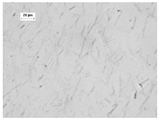
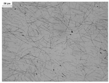
- 238000000879 optical micrograph Methods 0.000 description 2
- 229920001282 polysaccharide Polymers 0.000 description 2
- 239000005017 polysaccharide Substances 0.000 description 2
- 239000007787 solid Substances 0.000 description 2
- 239000000126 substance Substances 0.000 description 2
- 239000000758 substrate Substances 0.000 description 2
- 238000002834 transmittance Methods 0.000 description 2
- LNAZSHAWQACDHT-XIYTZBAFSA-N (2r,3r,4s,5r,6s)-4,5-dimethoxy-2-(methoxymethyl)-3-[(2s,3r,4s,5r,6r)-3,4,5-trimethoxy-6-(methoxymethyl)oxan-2-yl]oxy-6-[(2r,3r,4s,5r,6r)-4,5,6-trimethoxy-2-(methoxymethyl)oxan-3-yl]oxyoxane Chemical compound CO[C@@H]1[C@@H](OC)[C@H](OC)[C@@H](COC)O[C@H]1O[C@H]1[C@H](OC)[C@@H](OC)[C@H](O[C@H]2[C@@H]([C@@H](OC)[C@H](OC)O[C@@H]2COC)OC)O[C@@H]1COC LNAZSHAWQACDHT-XIYTZBAFSA-N 0.000 description 1
- 229920002134 Carboxymethyl cellulose Polymers 0.000 description 1
- 229920008347 Cellulose acetate propionate Polymers 0.000 description 1
- DQEFEBPAPFSJLV-UHFFFAOYSA-N Cellulose propionate Chemical compound CCC(=O)OCC1OC(OC(=O)CC)C(OC(=O)CC)C(OC(=O)CC)C1OC1C(OC(=O)CC)C(OC(=O)CC)C(OC(=O)CC)C(COC(=O)CC)O1 DQEFEBPAPFSJLV-UHFFFAOYSA-N 0.000 description 1
- 229920002284 Cellulose triacetate Polymers 0.000 description 1
- 229920000896 Ethulose Polymers 0.000 description 1
- 239000001856 Ethyl cellulose Substances 0.000 description 1
- ZZSNKZQZMQGXPY-UHFFFAOYSA-N Ethyl cellulose Chemical compound CCOCC1OC(OC)C(OCC)C(OCC)C1OC1C(O)C(O)C(OC)C(CO)O1 ZZSNKZQZMQGXPY-UHFFFAOYSA-N 0.000 description 1
- 239000001859 Ethyl hydroxyethyl cellulose Substances 0.000 description 1
- 229920000663 Hydroxyethyl cellulose Polymers 0.000 description 1
- 239000004354 Hydroxyethyl cellulose Substances 0.000 description 1
- 229920001479 Hydroxyethyl methyl cellulose Polymers 0.000 description 1
- 229920002153 Hydroxypropyl cellulose Polymers 0.000 description 1
- NNLVGZFZQQXQNW-ADJNRHBOSA-N [(2r,3r,4s,5r,6s)-4,5-diacetyloxy-3-[(2s,3r,4s,5r,6r)-3,4,5-triacetyloxy-6-(acetyloxymethyl)oxan-2-yl]oxy-6-[(2r,3r,4s,5r,6s)-4,5,6-triacetyloxy-2-(acetyloxymethyl)oxan-3-yl]oxyoxan-2-yl]methyl acetate Chemical compound O([C@@H]1O[C@@H]([C@H]([C@H](OC(C)=O)[C@H]1OC(C)=O)O[C@H]1[C@@H]([C@@H](OC(C)=O)[C@H](OC(C)=O)[C@@H](COC(C)=O)O1)OC(C)=O)COC(=O)C)[C@@H]1[C@@H](COC(C)=O)O[C@@H](OC(C)=O)[C@H](OC(C)=O)[C@H]1OC(C)=O NNLVGZFZQQXQNW-ADJNRHBOSA-N 0.000 description 1
- 238000013459 approach Methods 0.000 description 1
- NSPSPMKCKIPQBH-UHFFFAOYSA-K bismuth;7,7-dimethyloctanoate Chemical compound [Bi+3].CC(C)(C)CCCCCC([O-])=O.CC(C)(C)CCCCCC([O-])=O.CC(C)(C)CCCCCC([O-])=O NSPSPMKCKIPQBH-UHFFFAOYSA-K 0.000 description 1
- 239000001768 carboxy methyl cellulose Substances 0.000 description 1
- 235000010948 carboxy methyl cellulose Nutrition 0.000 description 1
- 239000008112 carboxymethyl-cellulose Substances 0.000 description 1
- 229920006218 cellulose propionate Polymers 0.000 description 1
- 230000000052 comparative effect Effects 0.000 description 1
- 239000004020 conductor Substances 0.000 description 1
- 238000007766 curtain coating Methods 0.000 description 1
- 238000013461 design Methods 0.000 description 1
- 238000003618 dip coating Methods 0.000 description 1
- 238000005516 engineering process Methods 0.000 description 1
- 150000002170 ethers Chemical class 0.000 description 1
- 229920001249 ethyl cellulose Polymers 0.000 description 1
- 235000019325 ethyl cellulose Nutrition 0.000 description 1
- 235000019326 ethyl hydroxyethyl cellulose Nutrition 0.000 description 1
- 239000001761 ethyl methyl cellulose Substances 0.000 description 1
- 235000010944 ethyl methyl cellulose Nutrition 0.000 description 1
- 238000002474 experimental method Methods 0.000 description 1
- 238000000605 extraction Methods 0.000 description 1
- 238000007765 extrusion coating Methods 0.000 description 1
- 238000007756 gravure coating Methods 0.000 description 1
- 235000019447 hydroxyethyl cellulose Nutrition 0.000 description 1
- 239000001863 hydroxypropyl cellulose Substances 0.000 description 1
- 235000010977 hydroxypropyl cellulose Nutrition 0.000 description 1
- 239000001866 hydroxypropyl methyl cellulose Substances 0.000 description 1
- 229920003088 hydroxypropyl methyl cellulose Polymers 0.000 description 1
- 235000010979 hydroxypropyl methyl cellulose Nutrition 0.000 description 1
- UFVKGYZPFZQRLF-UHFFFAOYSA-N hydroxypropyl methyl cellulose Chemical compound OC1C(O)C(OC)OC(CO)C1OC1C(O)C(O)C(OC2C(C(O)C(OC3C(C(O)C(O)C(CO)O3)O)C(CO)O2)O)C(CO)O1 UFVKGYZPFZQRLF-UHFFFAOYSA-N 0.000 description 1
- RHZWSUVWRRXEJF-UHFFFAOYSA-N indium tin Chemical compound [In].[Sn] RHZWSUVWRRXEJF-UHFFFAOYSA-N 0.000 description 1
- AMGQUBHHOARCQH-UHFFFAOYSA-N indium;oxotin Chemical compound [In].[Sn]=O AMGQUBHHOARCQH-UHFFFAOYSA-N 0.000 description 1
- 229960004592 isopropanol Drugs 0.000 description 1
- 238000004020 luminiscence type Methods 0.000 description 1
- 239000000463 material Substances 0.000 description 1
- 238000005259 measurement Methods 0.000 description 1
- 229920000609 methyl cellulose Polymers 0.000 description 1
- 239000001923 methylcellulose Substances 0.000 description 1
- 235000010981 methylcellulose Nutrition 0.000 description 1
- 239000000203 mixture Substances 0.000 description 1
- 238000012986 modification Methods 0.000 description 1
- 230000004048 modification Effects 0.000 description 1
- 239000003960 organic solvent Substances 0.000 description 1
- 229920001228 polyisocyanate Polymers 0.000 description 1
- 239000005056 polyisocyanate Substances 0.000 description 1
- 229920005596 polymer binder Polymers 0.000 description 1
- 239000002491 polymer binding agent Substances 0.000 description 1
- 238000006116 polymerization reaction Methods 0.000 description 1
- 229940090181 propyl acetate Drugs 0.000 description 1
- 238000007767 slide coating Methods 0.000 description 1
- 238000007764 slot die coating Methods 0.000 description 1
- 239000002904 solvent Substances 0.000 description 1
- 238000004528 spin coating Methods 0.000 description 1
- 238000007592 spray painting technique Methods 0.000 description 1
- 238000010345 tape casting Methods 0.000 description 1
- 229920001187 thermosetting polymer Polymers 0.000 description 1
- 239000004634 thermosetting polymer Substances 0.000 description 1
- 238000012546 transfer Methods 0.000 description 1
Images
Classifications
-
- H—ELECTRICITY
- H05—ELECTRIC TECHNIQUES NOT OTHERWISE PROVIDED FOR
- H05K—PRINTED CIRCUITS; CASINGS OR CONSTRUCTIONAL DETAILS OF ELECTRIC APPARATUS; MANUFACTURE OF ASSEMBLAGES OF ELECTRICAL COMPONENTS
- H05K1/00—Printed circuits
- H05K1/02—Details
- H05K1/09—Use of materials for the conductive, e.g. metallic pattern
- H05K1/092—Dispersed materials, e.g. conductive pastes or inks
- H05K1/095—Dispersed materials, e.g. conductive pastes or inks for polymer thick films, i.e. having a permanent organic polymeric binder
-
- B—PERFORMING OPERATIONS; TRANSPORTING
- B41—PRINTING; LINING MACHINES; TYPEWRITERS; STAMPS
- B41M—PRINTING, DUPLICATING, MARKING, OR COPYING PROCESSES; COLOUR PRINTING
- B41M1/00—Inking and printing with a printer's forme
- B41M1/10—Intaglio printing ; Gravure printing
-
- H—ELECTRICITY
- H01—ELECTRIC ELEMENTS
- H01B—CABLES; CONDUCTORS; INSULATORS; SELECTION OF MATERIALS FOR THEIR CONDUCTIVE, INSULATING OR DIELECTRIC PROPERTIES
- H01B1/00—Conductors or conductive bodies characterised by the conductive materials; Selection of materials as conductors
- H01B1/20—Conductive material dispersed in non-conductive organic material
- H01B1/22—Conductive material dispersed in non-conductive organic material the conductive material comprising metals or alloys
-
- H—ELECTRICITY
- H05—ELECTRIC TECHNIQUES NOT OTHERWISE PROVIDED FOR
- H05K—PRINTED CIRCUITS; CASINGS OR CONSTRUCTIONAL DETAILS OF ELECTRIC APPARATUS; MANUFACTURE OF ASSEMBLAGES OF ELECTRICAL COMPONENTS
- H05K2201/00—Indexing scheme relating to printed circuits covered by H05K1/00
- H05K2201/01—Dielectrics
- H05K2201/0104—Properties and characteristics in general
- H05K2201/0108—Transparent
-
- H—ELECTRICITY
- H05—ELECTRIC TECHNIQUES NOT OTHERWISE PROVIDED FOR
- H05K—PRINTED CIRCUITS; CASINGS OR CONSTRUCTIONAL DETAILS OF ELECTRIC APPARATUS; MANUFACTURE OF ASSEMBLAGES OF ELECTRICAL COMPONENTS
- H05K2201/00—Indexing scheme relating to printed circuits covered by H05K1/00
- H05K2201/02—Fillers; Particles; Fibers; Reinforcement materials
- H05K2201/0203—Fillers and particles
- H05K2201/0242—Shape of an individual particle
- H05K2201/0248—Needles or elongated particles; Elongated cluster of chemically bonded particles
-
- H—ELECTRICITY
- H05—ELECTRIC TECHNIQUES NOT OTHERWISE PROVIDED FOR
- H05K—PRINTED CIRCUITS; CASINGS OR CONSTRUCTIONAL DETAILS OF ELECTRIC APPARATUS; MANUFACTURE OF ASSEMBLAGES OF ELECTRICAL COMPONENTS
- H05K2201/00—Indexing scheme relating to printed circuits covered by H05K1/00
- H05K2201/02—Fillers; Particles; Fibers; Reinforcement materials
- H05K2201/0203—Fillers and particles
- H05K2201/0242—Shape of an individual particle
- H05K2201/026—Nanotubes or nanowires
-
- H—ELECTRICITY
- H05—ELECTRIC TECHNIQUES NOT OTHERWISE PROVIDED FOR
- H05K—PRINTED CIRCUITS; CASINGS OR CONSTRUCTIONAL DETAILS OF ELECTRIC APPARATUS; MANUFACTURE OF ASSEMBLAGES OF ELECTRICAL COMPONENTS
- H05K3/00—Apparatus or processes for manufacturing printed circuits
- H05K3/10—Apparatus or processes for manufacturing printed circuits in which conductive material is applied to the insulating support in such a manner as to form the desired conductive pattern
- H05K3/12—Apparatus or processes for manufacturing printed circuits in which conductive material is applied to the insulating support in such a manner as to form the desired conductive pattern using thick film techniques, e.g. printing techniques to apply the conductive material or similar techniques for applying conductive paste or ink patterns
- H05K3/1275—Apparatus or processes for manufacturing printed circuits in which conductive material is applied to the insulating support in such a manner as to form the desired conductive pattern using thick film techniques, e.g. printing techniques to apply the conductive material or similar techniques for applying conductive paste or ink patterns by other printing techniques, e.g. letterpress printing, intaglio printing, lithographic printing, offset printing
Landscapes
- Chemical & Material Sciences (AREA)
- Dispersion Chemistry (AREA)
- Engineering & Computer Science (AREA)
- Microelectronics & Electronic Packaging (AREA)
- Spectroscopy & Molecular Physics (AREA)
- Physics & Mathematics (AREA)
- Inks, Pencil-Leads, Or Crayons (AREA)
- Conductive Materials (AREA)
- Non-Insulated Conductors (AREA)
- Printing Methods (AREA)
- Manufacturing Of Electric Cables (AREA)
- Parts Printed On Printed Circuit Boards (AREA)
- Application Of Or Painting With Fluid Materials (AREA)
Applications Claiming Priority (5)
| Application Number | Priority Date | Filing Date | Title |
|---|---|---|---|
| US42321410P | 2010-12-15 | 2010-12-15 | |
| US61/423,214 | 2010-12-15 | ||
| US13/294,355 US8763525B2 (en) | 2010-12-15 | 2011-11-11 | Gravure printing of transparent conductive films containing networks of metal nanoparticles |
| US13/294,355 | 2011-11-11 | ||
| PCT/US2011/060492 WO2012082281A1 (en) | 2010-12-15 | 2011-11-12 | Gravure printing of transparent conductive films containing networks of metal nanoparticles |
Publications (1)
| Publication Number | Publication Date |
|---|---|
| KR20140010000A true KR20140010000A (ko) | 2014-01-23 |
Family
ID=46232665
Family Applications (1)
| Application Number | Title | Priority Date | Filing Date |
|---|---|---|---|
| KR1020137015440A Withdrawn KR20140010000A (ko) | 2010-12-15 | 2011-11-12 | 금속 나노입자 망 함유 투명 전도성 필름의 그라비어 인쇄 |
Country Status (7)
Families Citing this family (10)
| Publication number | Priority date | Publication date | Assignee | Title |
|---|---|---|---|---|
| US9441117B2 (en) * | 2012-03-20 | 2016-09-13 | Basf Se | Mixtures, methods and compositions pertaining to conductive materials |
| US9920207B2 (en) | 2012-06-22 | 2018-03-20 | C3Nano Inc. | Metal nanostructured networks and transparent conductive material |
| US10029916B2 (en) | 2012-06-22 | 2018-07-24 | C3Nano Inc. | Metal nanowire networks and transparent conductive material |
| US10020807B2 (en) | 2013-02-26 | 2018-07-10 | C3Nano Inc. | Fused metal nanostructured networks, fusing solutions with reducing agents and methods for forming metal networks |
| US11343911B1 (en) | 2014-04-11 | 2022-05-24 | C3 Nano, Inc. | Formable transparent conductive films with metal nanowires |
| WO2015157741A2 (en) * | 2014-04-11 | 2015-10-15 | Cambrios Technologies Corporation | Methods of controlling nanowire morphology |
| US9183968B1 (en) * | 2014-07-31 | 2015-11-10 | C3Nano Inc. | Metal nanowire inks for the formation of transparent conductive films with fused networks |
| CN112930575B (zh) | 2019-05-31 | 2022-06-07 | 昭和电工株式会社 | 透明导电膜的制造方法 |
| WO2021131099A1 (ja) | 2019-12-27 | 2021-07-01 | 昭和電工株式会社 | 透明導電フィルムの製造方法 |
| JP6855648B1 (ja) | 2019-12-27 | 2021-04-07 | 昭和電工株式会社 | 透明導電フィルムの製造方法 |
Family Cites Families (14)
| Publication number | Priority date | Publication date | Assignee | Title |
|---|---|---|---|---|
| EP1502154B1 (en) * | 2001-12-17 | 2009-02-18 | Northwestern University | Patterning of solid state features by direct write nanolithographic printing |
| US6872645B2 (en) * | 2002-04-02 | 2005-03-29 | Nanosys, Inc. | Methods of positioning and/or orienting nanostructures |
| AU2005325265A1 (en) * | 2004-07-07 | 2006-07-27 | Nanosys, Inc. | Systems and methods for harvesting and integrating nanowires |
| SG150514A1 (en) * | 2005-08-12 | 2009-03-30 | Cambrios Technologies Corp | Nanowires-based transparent conductors |
| US8018568B2 (en) | 2006-10-12 | 2011-09-13 | Cambrios Technologies Corporation | Nanowire-based transparent conductors and applications thereof |
| KR101545219B1 (ko) * | 2006-10-12 | 2015-08-18 | 캄브리오스 테크놀로지즈 코포레이션 | 나노와이어 기반의 투명 도전체 및 그의 응용 |
| EP2147466B9 (en) * | 2007-04-20 | 2014-07-16 | Cambrios Technologies Corporation | Composite transparent conductors |
| JP2009062523A (ja) * | 2007-08-10 | 2009-03-26 | Think Laboratory Co Ltd | 導電性インキ組成物 |
| GB0717055D0 (en) * | 2007-09-01 | 2007-10-17 | Eastman Kodak Co | An electronic device |
| WO2009063744A1 (ja) * | 2007-11-16 | 2009-05-22 | Konica Minolta Holdings, Inc. | 金属ナノワイヤの製造方法、金属ナノワイヤ及び透明導電体 |
| CN101553084B (zh) * | 2008-04-01 | 2010-12-08 | 富葵精密组件(深圳)有限公司 | 线路基板及线路基板的制作方法 |
| US20100197068A1 (en) * | 2008-10-30 | 2010-08-05 | Hak Fei Poon | Hybrid Transparent Conductive Electrode |
| JP2010250110A (ja) | 2009-04-16 | 2010-11-04 | Fujifilm Corp | 感光性組成物、並びに透明導電膜、表示素子及び集積型太陽電池 |
| JP5609008B2 (ja) * | 2009-05-12 | 2014-10-22 | コニカミノルタ株式会社 | 透明導電フィルム、透明導電フィルムの製造方法及び電子デバイス用透明電極 |
-
2011
- 2011-11-11 US US13/294,355 patent/US8763525B2/en not_active Expired - Fee Related
- 2011-11-12 KR KR1020137015440A patent/KR20140010000A/ko not_active Withdrawn
- 2011-11-12 EP EP11802185.6A patent/EP2653016A1/en not_active Withdrawn
- 2011-11-12 CN CN201180060685.3A patent/CN103262664B/zh not_active Expired - Fee Related
- 2011-11-12 WO PCT/US2011/060492 patent/WO2012082281A1/en active Application Filing
- 2011-11-12 JP JP2013544490A patent/JP5856625B2/ja not_active Expired - Fee Related
- 2011-12-02 TW TW100144465A patent/TW201231297A/zh unknown
Also Published As
| Publication number | Publication date |
|---|---|
| JP2014507746A (ja) | 2014-03-27 |
| JP5856625B2 (ja) | 2016-02-10 |
| CN103262664B (zh) | 2016-05-18 |
| WO2012082281A1 (en) | 2012-06-21 |
| EP2653016A1 (en) | 2013-10-23 |
| US20120152135A1 (en) | 2012-06-21 |
| US8763525B2 (en) | 2014-07-01 |
| TW201231297A (en) | 2012-08-01 |
| CN103262664A (zh) | 2013-08-21 |
Similar Documents
| Publication | Publication Date | Title |
|---|---|---|
| KR20140010000A (ko) | 금속 나노입자 망 함유 투명 전도성 필름의 그라비어 인쇄 | |
| KR102032108B1 (ko) | 금속성 나노섬유 잉크, 실질적으로 투명한 전도체, 및 제조 방법 | |
| JP5818822B2 (ja) | 増加ヘイズを有するナノ構造系透明導電体およびそれを備えるデバイス | |
| KR102254683B1 (ko) | 패턴화된 나노와이어 투명 전도체들에 대한 전자 컴포넌트들의 본딩 | |
| US20150056382A1 (en) | Transparent conductive ink and transparent conductive pattern forming method | |
| KR102264357B1 (ko) | 패턴화된 나노와이어 투명 전도체 상의 인쇄된 전도성 패턴을 위한 보호 코팅 | |
| CN110415865A (zh) | 一种光学一致透明导电薄膜及其制备方法 | |
| JP2016509332A (ja) | 基板上に透明導電体を製作する方法 | |
| US20220098738A1 (en) | Metallic Nanofiber Ink, Substantially Transparent Conductor, and Fabrication Method | |
| WO2012061399A1 (en) | Coating compositions for forming nanocomposite films | |
| WO2010018733A1 (ja) | 透明電極、有機エレクトロルミネッセンス素子及び透明電極の製造方法 | |
| CN113409991B (zh) | 柔性复合导电膜及其制备方法和应用 | |
| JP2019517053A (ja) | 金属相互連結部への向上した接着性を有するナノワイヤ接触パッド | |
| JP2020061372A (ja) | 透明コンダクタ、及び、透明コンダクタを製作するプロセス | |
| KR20140147975A (ko) | 전도성 잉크 조성물, 이를 포함하는 투명 전도성 필름 및 투명 전도성 필름의 제조방법 | |
| CN111883286A (zh) | 一种透明导电膜的制备方法及透明导电膜 | |
| CN116875086A (zh) | 一种透明电磁屏蔽涂层材料及其制备方法 | |
| US20140262443A1 (en) | Hybrid patterned nanostructure transparent conductors | |
| CN116259434B (zh) | 一种低阻导电银浆料、导电膜及导电膜的制备方法 | |
| JP5917912B2 (ja) | 銀導電膜およびその製造方法 | |
| CN114171241A (zh) | 一种导电结构及其制备方法、由其制备的电子设备 |
Legal Events
| Date | Code | Title | Description |
|---|---|---|---|
| PA0105 | International application |
Patent event date: 20130614 Patent event code: PA01051R01D Comment text: International Patent Application |
|
| PG1501 | Laying open of application | ||
| PC1203 | Withdrawal of no request for examination | ||
| WITN | Application deemed withdrawn, e.g. because no request for examination was filed or no examination fee was paid |