KR20140006039A - 광학적 메트롤로지 및 센서 디바이스를 이용한 에칭 프로세스 제어 방법 및 시스템 - Google Patents
광학적 메트롤로지 및 센서 디바이스를 이용한 에칭 프로세스 제어 방법 및 시스템 Download PDFInfo
- Publication number
- KR20140006039A KR20140006039A KR1020137024624A KR20137024624A KR20140006039A KR 20140006039 A KR20140006039 A KR 20140006039A KR 1020137024624 A KR1020137024624 A KR 1020137024624A KR 20137024624 A KR20137024624 A KR 20137024624A KR 20140006039 A KR20140006039 A KR 20140006039A
- Authority
- KR
- South Korea
- Prior art keywords
- etch
- measurement
- stage
- etch stage
- optical metrology
- Prior art date
- Legal status (The legal status is an assumption and is not a legal conclusion. Google has not performed a legal analysis and makes no representation as to the accuracy of the status listed.)
- Ceased
Links
Images


Classifications
-
- H—ELECTRICITY
- H10—SEMICONDUCTOR DEVICES; ELECTRIC SOLID-STATE DEVICES NOT OTHERWISE PROVIDED FOR
- H10P—GENERIC PROCESSES OR APPARATUS FOR THE MANUFACTURE OR TREATMENT OF DEVICES COVERED BY CLASS H10
- H10P72/00—Handling or holding of wafers, substrates or devices during manufacture or treatment thereof
- H10P72/04—Apparatus for manufacture or treatment
- H10P72/0402—Apparatus for fluid treatment
- H10P72/0418—Apparatus for fluid treatment for etching
- H10P72/0421—Apparatus for fluid treatment for etching for drying etching
-
- H—ELECTRICITY
- H01—ELECTRIC ELEMENTS
- H01J—ELECTRIC DISCHARGE TUBES OR DISCHARGE LAMPS
- H01J37/00—Discharge tubes with provision for introducing objects or material to be exposed to the discharge, e.g. for the purpose of examination or processing thereof
- H01J37/32—Gas-filled discharge tubes
- H01J37/32917—Plasma diagnostics
- H01J37/32935—Monitoring and controlling tubes by information coming from the object and/or discharge
-
- H—ELECTRICITY
- H10—SEMICONDUCTOR DEVICES; ELECTRIC SOLID-STATE DEVICES NOT OTHERWISE PROVIDED FOR
- H10P—GENERIC PROCESSES OR APPARATUS FOR THE MANUFACTURE OR TREATMENT OF DEVICES COVERED BY CLASS H10
- H10P50/00—Etching of wafers, substrates or parts of devices
- H10P50/20—Dry etching; Plasma etching; Reactive-ion etching
- H10P50/24—Dry etching; Plasma etching; Reactive-ion etching of semiconductor materials
- H10P50/242—Dry etching; Plasma etching; Reactive-ion etching of semiconductor materials of Group IV materials
-
- H—ELECTRICITY
- H10—SEMICONDUCTOR DEVICES; ELECTRIC SOLID-STATE DEVICES NOT OTHERWISE PROVIDED FOR
- H10P—GENERIC PROCESSES OR APPARATUS FOR THE MANUFACTURE OR TREATMENT OF DEVICES COVERED BY CLASS H10
- H10P72/00—Handling or holding of wafers, substrates or devices during manufacture or treatment thereof
- H10P72/06—Apparatus for monitoring, sorting, marking, testing or measuring
- H10P72/0604—Process monitoring, e.g. flow or thickness monitoring
-
- H—ELECTRICITY
- H10—SEMICONDUCTOR DEVICES; ELECTRIC SOLID-STATE DEVICES NOT OTHERWISE PROVIDED FOR
- H10P—GENERIC PROCESSES OR APPARATUS FOR THE MANUFACTURE OR TREATMENT OF DEVICES COVERED BY CLASS H10
- H10P72/00—Handling or holding of wafers, substrates or devices during manufacture or treatment thereof
- H10P72/06—Apparatus for monitoring, sorting, marking, testing or measuring
- H10P72/0612—Production flow monitoring, e.g. for increasing throughput
-
- H—ELECTRICITY
- H10—SEMICONDUCTOR DEVICES; ELECTRIC SOLID-STATE DEVICES NOT OTHERWISE PROVIDED FOR
- H10P—GENERIC PROCESSES OR APPARATUS FOR THE MANUFACTURE OR TREATMENT OF DEVICES COVERED BY CLASS H10
- H10P74/00—Testing or measuring during manufacture or treatment of wafers, substrates or devices
- H10P74/20—Testing or measuring during manufacture or treatment of wafers, substrates or devices characterised by the properties tested or measured, e.g. structural or electrical properties
- H10P74/203—Structural properties, e.g. testing or measuring thicknesses, line widths, warpage, bond strengths or physical defects
-
- H—ELECTRICITY
- H10—SEMICONDUCTOR DEVICES; ELECTRIC SOLID-STATE DEVICES NOT OTHERWISE PROVIDED FOR
- H10P—GENERIC PROCESSES OR APPARATUS FOR THE MANUFACTURE OR TREATMENT OF DEVICES COVERED BY CLASS H10
- H10P74/00—Testing or measuring during manufacture or treatment of wafers, substrates or devices
- H10P74/23—Testing or measuring during manufacture or treatment of wafers, substrates or devices characterised by multiple measurements, corrections, marking or sorting processes
Landscapes
- Engineering & Computer Science (AREA)
- Physics & Mathematics (AREA)
- Plasma & Fusion (AREA)
- Chemical & Material Sciences (AREA)
- Analytical Chemistry (AREA)
- Drying Of Semiconductors (AREA)
- Investigating Or Analysing Materials By Optical Means (AREA)
- Automation & Control Theory (AREA)
Applications Claiming Priority (3)
| Application Number | Priority Date | Filing Date | Title |
|---|---|---|---|
| US13/029,349 | 2011-02-17 | ||
| US13/029,349 US8193007B1 (en) | 2011-02-17 | 2011-02-17 | Etch process control using optical metrology and sensor devices |
| PCT/US2012/025746 WO2012112959A1 (en) | 2011-02-17 | 2012-02-17 | Etch process control using optical metrology and sensor devices |
Related Child Applications (1)
| Application Number | Title | Priority Date | Filing Date |
|---|---|---|---|
| KR1020177025199A Division KR20170107094A (ko) | 2011-02-17 | 2012-02-17 | 광학적 메트롤로지 및 센서 디바이스를 이용한 에칭 프로세스 제어 방법 및 시스템 |
Publications (1)
| Publication Number | Publication Date |
|---|---|
| KR20140006039A true KR20140006039A (ko) | 2014-01-15 |
Family
ID=46148020
Family Applications (2)
| Application Number | Title | Priority Date | Filing Date |
|---|---|---|---|
| KR1020137024624A Ceased KR20140006039A (ko) | 2011-02-17 | 2012-02-17 | 광학적 메트롤로지 및 센서 디바이스를 이용한 에칭 프로세스 제어 방법 및 시스템 |
| KR1020177025199A Ceased KR20170107094A (ko) | 2011-02-17 | 2012-02-17 | 광학적 메트롤로지 및 센서 디바이스를 이용한 에칭 프로세스 제어 방법 및 시스템 |
Family Applications After (1)
| Application Number | Title | Priority Date | Filing Date |
|---|---|---|---|
| KR1020177025199A Ceased KR20170107094A (ko) | 2011-02-17 | 2012-02-17 | 광학적 메트롤로지 및 센서 디바이스를 이용한 에칭 프로세스 제어 방법 및 시스템 |
Country Status (5)
| Country | Link |
|---|---|
| US (1) | US8193007B1 (https=) |
| JP (1) | JP6019043B2 (https=) |
| KR (2) | KR20140006039A (https=) |
| TW (1) | TWI464818B (https=) |
| WO (1) | WO2012112959A1 (https=) |
Cited By (1)
| Publication number | Priority date | Publication date | Assignee | Title |
|---|---|---|---|---|
| KR20190059329A (ko) * | 2016-10-21 | 2019-05-30 | 케이엘에이-텐코 코포레이션 | 총 측정 불확도의 정량화 및 감소 |
Families Citing this family (20)
| Publication number | Priority date | Publication date | Assignee | Title |
|---|---|---|---|---|
| US8445296B2 (en) * | 2011-07-22 | 2013-05-21 | Taiwan Semiconductor Manufacturing Company, Ltd. | Apparatus and methods for end point determination in reactive ion etching |
| US9287097B2 (en) * | 2011-11-30 | 2016-03-15 | Sony Corporation | Predicting ultraviolet ray damage with visible wavelength spectroscopy during a semiconductor manufacturing process |
| US9875946B2 (en) | 2013-04-19 | 2018-01-23 | Kla-Tencor Corporation | On-device metrology |
| NL2013417A (en) | 2013-10-02 | 2015-04-07 | Asml Netherlands Bv | Methods & apparatus for obtaining diagnostic information relating to an industrial process. |
| US10217681B1 (en) * | 2014-08-06 | 2019-02-26 | American Air Liquide, Inc. | Gases for low damage selective silicon nitride etching |
| US20160240366A1 (en) * | 2015-02-17 | 2016-08-18 | Infineon Technologies Ag | Processing of Semiconductor Devices |
| US10386829B2 (en) * | 2015-09-18 | 2019-08-20 | Kla-Tencor Corporation | Systems and methods for controlling an etch process |
| US10192763B2 (en) * | 2015-10-05 | 2019-01-29 | Applied Materials, Inc. | Methodology for chamber performance matching for semiconductor equipment |
| WO2018163396A1 (ja) * | 2017-03-10 | 2018-09-13 | 三菱電機株式会社 | 半導体製造装置および半導体製造方法 |
| US10784174B2 (en) * | 2017-10-13 | 2020-09-22 | Lam Research Corporation | Method and apparatus for determining etch process parameters |
| US11164768B2 (en) * | 2018-04-27 | 2021-11-02 | Kla Corporation | Process-induced displacement characterization during semiconductor production |
| JP2020181959A (ja) | 2019-04-26 | 2020-11-05 | 東京エレクトロン株式会社 | 学習方法、管理装置および管理プログラム |
| JP7413081B2 (ja) * | 2020-02-28 | 2024-01-15 | 東京エレクトロン株式会社 | 基板処理システム |
| GB202010471D0 (en) * | 2020-07-08 | 2020-08-19 | Univ Exeter | Control of processing equipment |
| US12106984B2 (en) * | 2021-11-23 | 2024-10-01 | Applied Materials, Inc. | Accelerating preventative maintenance recovery and recipe optimizing using machine-learning based algorithm |
| US20230163001A1 (en) * | 2021-11-23 | 2023-05-25 | Applied Materials, Inc. | Method to eliminate first wafer effects on semiconductor process chambers |
| CN114724943A (zh) * | 2022-03-18 | 2022-07-08 | 福建晶安光电有限公司 | 一种等离子体蚀刻方法及系统 |
| US12400888B2 (en) * | 2022-03-31 | 2025-08-26 | Tokyo Electron Limited | Data fusion of multiple sensors |
| KR102894716B1 (ko) * | 2023-09-14 | 2025-12-03 | 주식회사 히타치하이테크 | 플라스마 처리 장치 및 플라스마 처리 방법 |
| WO2026047926A1 (ja) * | 2024-08-29 | 2026-03-05 | 株式会社日立ハイテク | プラズマ処理・制御装置およびプラズマ処理・制御方法 |
Family Cites Families (21)
| Publication number | Priority date | Publication date | Assignee | Title |
|---|---|---|---|---|
| US5288367A (en) | 1993-02-01 | 1994-02-22 | International Business Machines Corporation | End-point detection |
| US5658423A (en) | 1995-11-27 | 1997-08-19 | International Business Machines Corporation | Monitoring and controlling plasma processes via optical emission using principal component analysis |
| US5862060A (en) | 1996-11-22 | 1999-01-19 | Uop Llc | Maintenance of process control by statistical analysis of product optical spectrum |
| US6943900B2 (en) | 2000-09-15 | 2005-09-13 | Timbre Technologies, Inc. | Generation of a library of periodic grating diffraction signals |
| US6785638B2 (en) | 2001-08-06 | 2004-08-31 | Timbre Technologies, Inc. | Method and system of dynamic learning through a regression-based library generation process |
| US7216045B2 (en) | 2002-06-03 | 2007-05-08 | Timbre Technologies, Inc. | Selection of wavelengths for integrated circuit optical metrology |
| US6979578B2 (en) | 2002-08-13 | 2005-12-27 | Lam Research Corporation | Process endpoint detection method using broadband reflectometry |
| US7352478B2 (en) | 2002-12-20 | 2008-04-01 | International Business Machines Corporation | Assessment and optimization for metrology instrument |
| US20040267397A1 (en) | 2003-06-27 | 2004-12-30 | Srinivas Doddi | Optical metrology of structures formed on semiconductor wafer using machine learning systems |
| US7158221B2 (en) * | 2003-12-23 | 2007-01-02 | Applied Materials, Inc. | Method and apparatus for performing limited area spectral analysis |
| US7065423B2 (en) * | 2004-07-08 | 2006-06-20 | Timbre Technologies, Inc. | Optical metrology model optimization for process control |
| KR20060005830A (ko) | 2004-07-14 | 2006-01-18 | 삼성전자주식회사 | 통합 슬롯이 탑재된 인쇄 회로 기판 |
| US20060112796A1 (en) | 2004-11-30 | 2006-06-01 | Chang-Ying Chen | Screwdriver with teethed head |
| US7467064B2 (en) | 2006-02-07 | 2008-12-16 | Timbre Technologies, Inc. | Transforming metrology data from a semiconductor treatment system using multivariate analysis |
| US7596422B2 (en) * | 2007-01-12 | 2009-09-29 | Tokyo Electron Limited | Determining one or more profile parameters of a structure using optical metrology and a correlation between profile models and key profile shape variables |
| CN101675495B (zh) * | 2007-02-02 | 2011-12-14 | 雷克萨斯研究有限公司 | 用于测量等离子体刻蚀工艺的工艺参数的方法和装置 |
| US7591600B2 (en) * | 2007-02-23 | 2009-09-22 | Tokyo Electron Limited | Method and system for monitoring photolithography processing based on a batch change in light sensitive material |
| US7742177B2 (en) | 2008-01-22 | 2010-06-22 | Tokyo Electron Limited | Noise-reduction metrology models |
| US7589845B1 (en) * | 2008-03-27 | 2009-09-15 | Tokyo Electron Limited | Process control using an optical metrology system optimized with signal criteria |
| US7761250B2 (en) | 2008-06-18 | 2010-07-20 | Tokyo Electron Limited | Optical metrology system optimized with design goals |
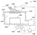
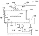
| US8173451B1 (en) * | 2011-02-16 | 2012-05-08 | Tokyo Electron Limited | Etch stage measurement system |
-
2011
- 2011-02-17 US US13/029,349 patent/US8193007B1/en active Active
-
2012
- 2012-02-17 JP JP2013554662A patent/JP6019043B2/ja active Active
- 2012-02-17 KR KR1020137024624A patent/KR20140006039A/ko not_active Ceased
- 2012-02-17 KR KR1020177025199A patent/KR20170107094A/ko not_active Ceased
- 2012-02-17 TW TW101105282A patent/TWI464818B/zh active
- 2012-02-17 WO PCT/US2012/025746 patent/WO2012112959A1/en not_active Ceased
Cited By (1)
| Publication number | Priority date | Publication date | Assignee | Title |
|---|---|---|---|---|
| KR20190059329A (ko) * | 2016-10-21 | 2019-05-30 | 케이엘에이-텐코 코포레이션 | 총 측정 불확도의 정량화 및 감소 |
Also Published As
| Publication number | Publication date |
|---|---|
| TW201241949A (en) | 2012-10-16 |
| WO2012112959A1 (en) | 2012-08-23 |
| KR20170107094A (ko) | 2017-09-22 |
| TWI464818B (zh) | 2014-12-11 |
| JP2014514727A (ja) | 2014-06-19 |
| JP6019043B2 (ja) | 2016-11-02 |
| US8193007B1 (en) | 2012-06-05 |
Similar Documents
| Publication | Publication Date | Title |
|---|---|---|
| US8193007B1 (en) | Etch process control using optical metrology and sensor devices | |
| US8173451B1 (en) | Etch stage measurement system | |
| JP7269296B2 (ja) | 方法およびエッチングシステム | |
| US10847430B2 (en) | Method of feature exaction from time-series of spectra to control endpoint of process | |
| JP3708031B2 (ja) | プラズマ処理装置および処理方法 | |
| CN104736744B (zh) | 使用多变量分析的等离子体蚀刻终点检测 | |
| US8257546B2 (en) | Method and system for monitoring an etch process | |
| US8173450B1 (en) | Method of designing an etch stage measurement system | |
| US20240255858A1 (en) | In situ sensor and logic for process control | |
| JP2006074067A (ja) | プラズマ処理装置および処理方法 | |
| JP4344674B2 (ja) | プラズマ処理装置 | |
| Barna et al. | In Situ Metrology | |
| Venugopal et al. | Manufacturability considerations in designing optical monitoring methods for control of plasma etch processes |
Legal Events
| Date | Code | Title | Description |
|---|---|---|---|
| PA0105 | International application |
St.27 status event code: A-0-1-A10-A15-nap-PA0105 |
|
| PG1501 | Laying open of application |
St.27 status event code: A-1-1-Q10-Q12-nap-PG1501 |
|
| R17-X000 | Change to representative recorded |
St.27 status event code: A-3-3-R10-R17-oth-X000 |
|
| A201 | Request for examination | ||
| AMND | Amendment | ||
| P11-X000 | Amendment of application requested |
St.27 status event code: A-2-2-P10-P11-nap-X000 |
|
| P13-X000 | Application amended |
St.27 status event code: A-2-2-P10-P13-nap-X000 |
|
| PA0201 | Request for examination |
St.27 status event code: A-1-2-D10-D11-exm-PA0201 |
|
| R17-X000 | Change to representative recorded |
St.27 status event code: A-3-3-R10-R17-oth-X000 |
|
| E902 | Notification of reason for refusal | ||
| PE0902 | Notice of grounds for rejection |
St.27 status event code: A-1-2-D10-D21-exm-PE0902 |
|
| AMND | Amendment | ||
| E13-X000 | Pre-grant limitation requested |
St.27 status event code: A-2-3-E10-E13-lim-X000 |
|
| P11-X000 | Amendment of application requested |
St.27 status event code: A-2-2-P10-P11-nap-X000 |
|
| P13-X000 | Application amended |
St.27 status event code: A-2-2-P10-P13-nap-X000 |
|
| E601 | Decision to refuse application | ||
| PE0601 | Decision on rejection of patent |
St.27 status event code: N-2-6-B10-B15-exm-PE0601 |
|
| X091 | Application refused [patent] | ||
| AMND | Amendment | ||
| E13-X000 | Pre-grant limitation requested |
St.27 status event code: A-2-3-E10-E13-lim-X000 |
|
| P11-X000 | Amendment of application requested |
St.27 status event code: A-2-2-P10-P11-nap-X000 |
|
| P13-X000 | Application amended |
St.27 status event code: A-2-2-P10-P13-nap-X000 |
|
| PX0901 | Re-examination |
St.27 status event code: A-2-3-E10-E12-rex-PX0901 |
|
| PX0601 | Decision of rejection after re-examination |
St.27 status event code: N-2-6-B10-B17-rex-PX0601 |
|
| X601 | Decision of rejection after re-examination | ||
| T11-X000 | Administrative time limit extension requested |
St.27 status event code: U-3-3-T10-T11-oth-X000 |
|
| T13-X000 | Administrative time limit extension granted |
St.27 status event code: U-3-3-T10-T13-oth-X000 |
|
| A107 | Divisional application of patent | ||
| J201 | Request for trial against refusal decision | ||
| PA0104 | Divisional application for international application |
St.27 status event code: A-0-1-A10-A18-div-PA0104 St.27 status event code: A-0-1-A10-A16-div-PA0104 |
|
| PJ0201 | Trial against decision of rejection |
St.27 status event code: A-3-3-V10-V11-apl-PJ0201 |
|
| J301 | Trial decision |
Free format text: TRIAL NUMBER: 2017101004298; TRIAL DECISION FOR APPEAL AGAINST DECISION TO DECLINE REFUSAL REQUESTED 20170907 Effective date: 20190226 |
|
| PJ1301 | Trial decision |
St.27 status event code: A-3-3-V10-V15-crt-PJ1301 Decision date: 20190226 Appeal event data comment text: Appeal Kind Category : Appeal against decision to decline refusal, Appeal Ground Text : 2013 7024624 Appeal request date: 20170907 Appellate body name: Patent Examination Board Decision authority category: Office appeal board Decision identifier: 2017101004298 |
|
| P22-X000 | Classification modified |
St.27 status event code: A-2-2-P10-P22-nap-X000 |