KR20130136548A - Actuator, optical scanner, and image generator - Google Patents
Actuator, optical scanner, and image generator Download PDFInfo
- Publication number
- KR20130136548A KR20130136548A KR1020137027783A KR20137027783A KR20130136548A KR 20130136548 A KR20130136548 A KR 20130136548A KR 1020137027783 A KR1020137027783 A KR 1020137027783A KR 20137027783 A KR20137027783 A KR 20137027783A KR 20130136548 A KR20130136548 A KR 20130136548A
- Authority
- KR
- South Korea
- Prior art keywords
- movable portion
- movable
- movable plate
- actuator
- optical scanner
- Prior art date
Links
Images


Classifications
-
- H—ELECTRICITY
- H02—GENERATION; CONVERSION OR DISTRIBUTION OF ELECTRIC POWER
- H02K—DYNAMO-ELECTRIC MACHINES
- H02K33/00—Motors with reciprocating, oscillating or vibrating magnet, armature or coil system
- H02K33/16—Motors with reciprocating, oscillating or vibrating magnet, armature or coil system with polarised armatures moving in alternate directions by reversal or energisation of a single coil system
-
- H—ELECTRICITY
- H02—GENERATION; CONVERSION OR DISTRIBUTION OF ELECTRIC POWER
- H02K—DYNAMO-ELECTRIC MACHINES
- H02K33/00—Motors with reciprocating, oscillating or vibrating magnet, armature or coil system
-
- B—PERFORMING OPERATIONS; TRANSPORTING
- B81—MICROSTRUCTURAL TECHNOLOGY
- B81B—MICROSTRUCTURAL DEVICES OR SYSTEMS, e.g. MICROMECHANICAL DEVICES
- B81B3/00—Devices comprising flexible or deformable elements, e.g. comprising elastic tongues or membranes
-
- G—PHYSICS
- G02—OPTICS
- G02B—OPTICAL ELEMENTS, SYSTEMS OR APPARATUS
- G02B26/00—Optical devices or arrangements for the control of light using movable or deformable optical elements
- G02B26/08—Optical devices or arrangements for the control of light using movable or deformable optical elements for controlling the direction of light
- G02B26/0816—Optical devices or arrangements for the control of light using movable or deformable optical elements for controlling the direction of light by means of one or more reflecting elements
- G02B26/0833—Optical devices or arrangements for the control of light using movable or deformable optical elements for controlling the direction of light by means of one or more reflecting elements the reflecting element being a micromechanical device, e.g. a MEMS mirror, DMD
- G02B26/085—Optical devices or arrangements for the control of light using movable or deformable optical elements for controlling the direction of light by means of one or more reflecting elements the reflecting element being a micromechanical device, e.g. a MEMS mirror, DMD the reflecting means being moved or deformed by electromagnetic means
-
- G—PHYSICS
- G02—OPTICS
- G02B—OPTICAL ELEMENTS, SYSTEMS OR APPARATUS
- G02B26/00—Optical devices or arrangements for the control of light using movable or deformable optical elements
- G02B26/08—Optical devices or arrangements for the control of light using movable or deformable optical elements for controlling the direction of light
- G02B26/10—Scanning systems
Landscapes
- Physics & Mathematics (AREA)
- Engineering & Computer Science (AREA)
- Power Engineering (AREA)
- General Physics & Mathematics (AREA)
- Optics & Photonics (AREA)
- Electromagnetism (AREA)
- Micromachines (AREA)
- Mechanical Optical Scanning Systems (AREA)
- Computer Hardware Design (AREA)
- Microelectronics & Electronic Packaging (AREA)
- Mechanical Light Control Or Optical Switches (AREA)
- Facsimile Scanning Arrangements (AREA)
Abstract
요동축 둘레에 요동 가능한 가동부와, 상기 가동부로부터 연장되고, 또한 상기 가동부의 요동에 따라 비틀림 변형되는 연결부와, 상기 연결부를 지지하는 지지부를 갖고, 상기 가동부는, 상기 가동부의 두께 방향으로부터의 평면에서 보아 십자 형상을 이루는 것을 특징으로 하는 액추에이터이다.A movable part that can swing around the swing shaft, a connecting part extending from the movable part and torsionally deformed in accordance with the swinging of the movable part, and a supporting part supporting the connecting part, wherein the movable part is in a plane from the thickness direction of the movable part. The actuator is characterized by forming a cross shape.
Description
본 발명은, 액추에이터, 광 스캐너 및 화상 형성 장치에 관한 것이다.The present invention relates to an actuator, an optical scanner, and an image forming apparatus.
액추에이터로서는, 비틀림 진동자를 사용한 것이 알려져 있다(예를 들어, 특허문헌 1 참조).As an actuator, what used the torsional vibrator is known (for example, refer patent document 1).
예를 들어, 특허문헌 1에는, 가동판(가동부)과, 지지 프레임(지지부)과, 가동판을 지지 프레임에 대해서 비틀림 회전 가능하게 지지하는 한 쌍의 탄성 지지부(연결부)를 갖고, 각 탄성 지지부가 2개의 막대(빔 부재)로 구성된 광 편향기가 개시되어 있다.For example,
이와 같은 가동판, 지지 프레임 및 한 쌍의 탄성 지지부는, 주면이 실리콘의 (100)면으로 구성된 실리콘 기판을 이방성 에칭함으로써 일체 형성된다.Such a movable plate, a support frame, and a pair of elastic supports are integrally formed by anisotropically etching a silicon substrate whose main surface is composed of the (100) plane of silicon.
또한, 특허문헌 1에 관한 광 편향기에서는, 가동판이 평면에서 보아 팔각형을 이루고 있다. 이와 같은 평면에서 보아 형상을 이루는 가동판은, 회전축(요동축)으로부터 떨어진 위치에서의 가동판의 중량을 작게 하여, 관성 모멘트를 저감할 수 있다고 하는 이점이 있다.Moreover, in the optical deflector which concerns on
그러나, 평면에서 보아 형상이 팔각형을 이루는 가동판은, 전술한 바와 같은 이방성 에칭을 사용해서 제조한 경우, 결정면과의 관계로부터, 형상의 변동이 크다.However, when a movable plate having an octagonal shape in plan view is produced using the anisotropic etching as described above, the shape variation is large from the relationship with the crystal plane.
본 발명의 목적은, 제조에 있어서의 가동부의 형상 변동을 종래보다도 작게 하여, 가동부의 요동시의 관성 모멘트를 저감할 수 있는 액추에이터, 광 스캐너 및 화상 형성 장치를 제공하는 데 있다.SUMMARY OF THE INVENTION An object of the present invention is to provide an actuator, an optical scanner, and an image forming apparatus which can reduce the shape variation of the movable part in manufacturing to a smaller level than the conventional one, and can reduce the moment of inertia at the time of swinging the movable part.
이와 같은 목적은, 하기의 본 발명에 의해 달성된다.Such an object is achieved by the following invention.
본 발명의 액추에이터는, 요동축 둘레에 요동 가능한 가동부와,The actuator of the present invention includes a movable part capable of swinging around a swing shaft,
상기 가동부로부터 연장되고, 또한 상기 가동부의 요동에 따라 비틀림 변형되는 연결부와,A connection portion extending from the movable portion and further twisted and deformed in accordance with the swing of the movable portion;
상기 연결부를 지지하는 지지부를 갖고,Having a support for supporting the connecting portion,
상기 가동부는, 상기 가동부의 두께 방향으로부터의 평면에서 보아 십자 형상을 이루는 것을 특징으로 한다.The movable portion is characterized by forming a cross shape in plan view from the thickness direction of the movable portion.
이와 같은 본 발명의 액추에이터에 따르면, 제조에 있어서의 가동부의 형상 변동을 작게 하여, 가동부의 요동시의 관성 모멘트를 저감할 수 있다.According to such an actuator of the present invention, the shape variation of the movable part in manufacturing can be reduced, and the moment of inertia at the time of swinging of the movable part can be reduced.
본 발명의 액추에이터에서는, 상기 가동부의 상기 두께 방향으로부터의 평면에서 보아 외형은, 주로, 상기 요동축에 평행한 선분과, 상기 요동축에 대해서 수직인 선분으로 구성되어 있는 것이 바람직하다.In the actuator of this invention, it is preferable that an external shape mainly consists of the line segment parallel to the said oscillation axis | shaft, and the line segment perpendicular | vertical to the said oscillation axis | shaft from the plane from the said thickness direction of the said movable part.
이에 의해, 제조에 있어서의 가동부의 형상 변동을 작게 할 수 있다.Thereby, the shape variation of the movable part in manufacture can be made small.
본 발명의 액추에이터에서는, 상기 가동부, 상기 지지부 및 상기 연결부는, 실리콘 기판을 이방성 에칭함으로써 형성된 것인 것이 바람직하다.In the actuator of this invention, it is preferable that the said movable part, the said support part, and the said connection part are formed by anisotropically etching a silicon substrate.
이에 의해, 형상 변동을 작게 하여, 가동부, 지지부 및 한 쌍의 연결부를 용이하게 형성할 수 있다.Thereby, shape change can be made small and a movable part, a support part, and a pair of connection part can be formed easily.
본 발명의 액추에이터에서는, 상기 가동부의 판면은 실리콘의 (100)면으로 구성되어 있는 것이 바람직하다.In the actuator of this invention, it is preferable that the plate surface of the said movable part is comprised from the (100) surface of silicon.
이에 의해, 판면이 (100)면으로 구성된 실리콘 기판을 이방성 에칭함으로써, 형상 변동을 작게 하여, 가동부, 지지부 및 한 쌍의 연결부를 용이하게 형성할 수 있다.Thereby, by anisotropically etching the silicon substrate whose plate surface is comprised from the (100) surface, shape change can be made small and a movable part, a support part, and a pair of connection part can be formed easily.
본 발명의 액추에이터에서는, 상기 가동부의 측면은, 주로, 실리콘의 (111)면으로 구성되어 있는 것이 바람직하다.In the actuator of this invention, it is preferable that the side surface of the said movable part is comprised mainly with the (111) plane of silicon.
이에 의해, 판면이 (100)면으로 구성된 실리콘 기판을 이방성 에칭함으로써, 실리콘의 (111)면을 에칭의 정지층으로서 이용하고, 형상 변동을 작게 하여, 가동부, 지지부 및 한 쌍의 연결부를 용이하게 형성할 수 있다.Thereby, by anisotropically etching the silicon substrate whose plate surface is comprised of the (100) surface, the (111) surface of silicon is used as a stop layer for etching, and shape change is made small, and a movable part, a support part, and a pair of connection part are easy. Can be formed.
본 발명의 액추에이터에서는, 상기 가동부의 측면에는, 상기 가동부의 판면에 직교하는 단면에서 V자 형상을 이루는 홈이 형성되어 있는 것이 바람직하다.In the actuator of this invention, it is preferable that the groove | channel which forms V shape in the cross section orthogonal to the plate surface of the said movable part is formed in the side surface of the said movable part.
이에 의해, 가동부의 관성 모멘트를 저감할 수 있다. 또한, 이와 같은 홈은, 판면이 (100)면으로 구성된 실리콘 기판을 이방성 에칭함으로써, 실리콘의 (111)면을 에칭의 정지층으로서 이용하고, 형상 변동을 작게 하여 가동부를 용이하게 형성할 수 있다.As a result, the moment of inertia of the movable portion can be reduced. In addition, such a groove can anisotropically etch a silicon substrate having a plate surface of (100) plane, thereby making it possible to easily form a movable portion by using a (111) plane of silicon as a stop layer for etching, to reduce the shape variation. .
본 발명의 액추에이터에서는, 상기 연결부의 표면은 실리콘의 (100)면 및 (111)면으로 구성되어 있는 것이 바람직하다.In the actuator of this invention, it is preferable that the surface of the said connection part is comprised by the (100) surface and (111) surface of silicone.
이에 의해, 실리콘의 (111)면을 에칭의 정지층으로서 이용하고, 형상 변동을 작게 하여 연결부를 용이하게 형성할 수 있다.Thereby, the (111) surface of silicon can be used as a stop layer for etching, and the connection can be easily formed by reducing the shape variation.
본 발명의 액추에이터에서는, 상기 가동부는, 상기 두께 방향으로부터의 평면에서 보아 상기 가동부의 상기 요동축에 대해서 대칭인 형상을 이루고 있는 것이 바람직하다.In the actuator of this invention, it is preferable that the said movable part has comprised the symmetrical shape with respect to the said oscillation axis of the said movable part by planar view from the said thickness direction.
이에 의해, 가동부의 무게 중심을 가동부의 요동축 상에 위치시켜, 가동부의 요동을 원활한 것으로 할 수 있다.Thereby, the center of gravity of the movable part can be positioned on the swinging shaft of the movable part, thereby making it possible to smooth the swinging of the movable part.
본 발명의 액추에이터에서는, 상기 가동부는, 상기 두께 방향으로부터의 평면에서 보아 상기 가동부의 중심을 지나고 또한 상기 가동부의 상기 요동축에 대해서 수직인 선분에 대해서 대칭인 형상을 이루고 있는 것이 바람직하다.In the actuator of this invention, it is preferable that the said movable part has the symmetrical shape with respect to the line segment which passes through the center of the said movable part in the plane from the said thickness direction, and is perpendicular to the said oscillation axis of the said movable part.
이에 의해, 가동부의 설계가 용이하게 된다.This facilitates the design of the movable portion.
본 발명의 액추에이터는, 요동축 둘레에 요동 가능한 가동부와,The actuator of the present invention includes a movable part capable of swinging around a swing shaft,
상기 가동부로부터 연장되고, 또한 상기 가동부의 요동에 따라 비틀림 변형되는 연결부와,A connection portion extending from the movable portion and further twisted and deformed in accordance with the swing of the movable portion;
상기 연결부를 지지하는 지지부를 갖고,Having a support for supporting the connecting portion,
상기 가동부는, 상기 가동부의 두께 방향으로부터의 평면에서 보아 사각형의 4개의 코너 부분이 각각 구형(矩形)으로 결손된 형상을 이루는 것을 특징으로 한다.The said movable part is characterized by the four corner | angular parts of a quadrangle formed in the shape of a rectangle each viewed from the plane from the thickness direction of the said movable part, It is characterized by the above-mentioned.
이와 같은 본 발명의 액추에이터에 따르면, 제조에 있어서의 가동부의 형상 변동을 작게 하여, 가동부의 요동시의 관성 모멘트를 저감할 수 있다.According to such an actuator of the present invention, the shape variation of the movable part in manufacturing can be reduced, and the moment of inertia at the time of swinging of the movable part can be reduced.
본 발명의 광 스캐너는, 광 반사성을 갖는 광 반사부를 구비하고, 또한 요동축 둘레에 요동 가능한 가동부와,An optical scanner of the present invention includes a movable portion having a light reflecting portion having light reflectivity and capable of oscillating around a swing shaft;
상기 가동부로부터 연장되고, 또한 상기 가동부의 요동에 따라 비틀림 변형되는 연결부와,A connection portion extending from the movable portion and further twisted and deformed in accordance with the swing of the movable portion;
상기 연결부를 지지하는 지지부를 갖고,Having a support for supporting the connecting portion,
상기 가동부는, 상기 가동부의 두께 방향으로부터의 평면에서 보아 십자 형상을 이루는 것을 특징으로 한다.The movable portion is characterized by forming a cross shape in plan view from the thickness direction of the movable portion.
이와 같이 구성된 광 스캐너에 따르면, 제조에 있어서의 가동부의 형상 변동을 작게 하여, 가동부의 요동시의 관성 모멘트를 저감할 수 있다.According to the optical scanner comprised in this way, the shape variation of the movable part in manufacture can be made small, and the moment of inertia at the time of oscillation of the movable part can be reduced.
본 발명의 광 스캐너는, 광 반사성을 갖는 광 반사부를 구비하고, 또한 요동축 둘레에 요동 가능한 가동부와,An optical scanner of the present invention includes a movable portion having a light reflecting portion having light reflectivity and capable of oscillating around a swing shaft;
상기 가동부로부터 연장되고, 또한 상기 가동부의 요동에 따라 비틀림 변형되는 연결부와,A connection portion extending from the movable portion and further twisted and deformed in accordance with the swing of the movable portion;
상기 연결부를 지지하는 지지부를 갖고,Having a support for supporting the connecting portion,
상기 가동부는, 상기 가동부의 두께 방향으로부터의 평면에서 보아 사각형의 4개의 코너 부분이 각각 구형으로 결손된 형상을 이루는 것을 특징으로 한다.The movable portion is characterized in that the four corner portions of the quadrangle are formed in a spherical shape in a plan view from the thickness direction of the movable portion.
이와 같이 구성된 광 스캐너에 따르면, 제조에 있어서의 가동부의 형상 변동을 작게 하여, 가동부의 요동시의 관성 모멘트를 저감할 수 있다.According to the optical scanner comprised in this way, the shape variation of the movable part in manufacture can be made small, and the moment of inertia at the time of oscillation of the movable part can be reduced.
본 발명의 화상 형성 장치는, 광을 출사하는 광원과,The image forming apparatus of the present invention includes a light source for emitting light,
상기 광원으로부터의 광을 주사하는 광 스캐너를 구비하고,An optical scanner for scanning light from the light source,
상기 광 스캐너는,The optical scanner,
광 반사성을 갖는 광 반사부를 구비하고, 또한 요동축 둘레에 요동 가능한 가동부와,A movable portion having a light reflecting portion having light reflectivity and capable of oscillating around a swing shaft;
상기 가동부로부터 연장되고, 또한 상기 가동부의 요동에 따라 비틀림 변형되는 연결부와,A connection portion extending from the movable portion and further twisted and deformed in accordance with the swing of the movable portion;
상기 연결부를 지지하는 지지부를 갖고,Having a support for supporting the connecting portion,
상기 가동부는, 상기 가동부의 두께 방향으로부터의 평면에서 보아 십자 형상을 이루는 것을 특징으로 한다.The movable portion is characterized by forming a cross shape in plan view from the thickness direction of the movable portion.
이와 같이 구성된 화상 형성 장치에 따르면, 제조에 있어서의 가동부의 형상 변동을 작게 하여, 가동부의 요동시의 관성 모멘트를 저감할 수 있다. 그로 인해, 저렴하게, 고품위의 화상을 얻을 수 있다.According to the image forming apparatus configured as described above, the shape variation of the movable part in manufacturing can be reduced, and the moment of inertia at the time of swinging of the movable part can be reduced. Therefore, a high quality image can be obtained inexpensively.
본 발명의 화상 형성 장치는, 광을 출사하는 광원과,The image forming apparatus of the present invention includes a light source for emitting light,
상기 광원으로부터의 광을 주사하는 광 스캐너를 구비하고,An optical scanner for scanning light from the light source,
상기 광 스캐너는,The optical scanner,
광 반사성을 갖는 광 반사부를 구비하고, 또한 요동축 둘레에 요동 가능한 가동부와,A movable portion having a light reflecting portion having light reflectivity and capable of oscillating around a swing shaft;
상기 가동부로부터 연장되고, 또한 상기 가동부의 요동에 따라 비틀림 변형되는 연결부와,A connection portion extending from the movable portion and further twisted and deformed in accordance with the swing of the movable portion;
상기 연결부를 지지하는 지지부를 갖고,Having a support for supporting the connecting portion,
상기 가동부는, 상기 가동부의 두께 방향으로부터의 평면에서 보아 사각형의 4개의 코너 부분이 각각 구형으로 결손된 형상을 이루는 것을 특징으로 한다.The movable portion is characterized in that the four corner portions of the quadrangle are formed in a spherical shape in a plan view from the thickness direction of the movable portion.
이와 같이 구성된 화상 형성 장치에 따르면, 제조에 있어서의 가동부의 형상 변동을 작게 하여, 가동부의 요동시의 관성 모멘트를 저감할 수 있다. 그로 인해, 저렴하게, 고품위의 화상을 얻을 수 있다.According to the image forming apparatus configured as described above, the shape variation of the movable part in manufacturing can be reduced, and the moment of inertia at the time of swinging of the movable part can be reduced. Therefore, a high quality image can be obtained inexpensively.
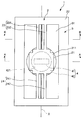
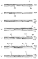
도 1은 본 발명의 제1 실시 형태에 관한 광 스캐너(액추에이터)를 도시하는 평면도이다.
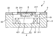
도 2는 도 1 중의 A-A선 단면도이다.
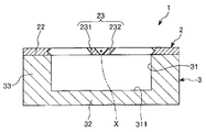
도 3은 도 1에 도시하는 광 스캐너에 구비된 가동판을 설명하기 위한 평면도이다.
도 4는 도 1 중의 B-B선 단면도이다.
도 5는 도 4의 부분 확대 단면도이다.
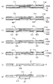
도 6은 도 1에 도시하는 광 스캐너의 제조 방법을 설명하는 단면도이다.
도 7은 도 1에 도시하는 광 스캐너의 제조 방법을 설명하는 단면도이다.
도 8은 도 1에 도시하는 광 스캐너의 제조 방법을 설명하는 단면도이다.
도 9는 도 8의 (e)에 도시하는 에칭 공정에 있어서의 연결부의 형성(마스크 어긋남이 없는 경우)을 설명하기 위한 도면이다.
도 10은 도 8의 (e)에 도시하는 에칭 공정에 있어서의 연결부의 형성(마스크 어긋남이 있는 경우)을 설명하기 위한 도면이다.
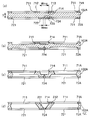
도 11은 본 발명의 제2 실시 형태에 관한 광 스캐너를 도시하는 평면도이다.
도 12는 도 11 중의 B-B선 부분 확대 단면도이다.
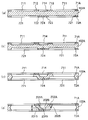
도 13은 본 발명의 제3 실시 형태에 관한 스캐너에 구비된 가동판을 설명하기 위한 평면도이다.
도 14는 본 발명의 제4 실시 형태에 관한 스캐너에 구비된 가동판을 설명하기 위한 평면도이다.
도 15는 본 발명의 화상 형성 장치의 구성의 일례를 나타내는 개략도이다.1 is a plan view showing an optical scanner (actuator) according to a first embodiment of the present invention.
2 is a cross-sectional view taken along the line AA in FIG. 1.
FIG. 3 is a plan view for explaining a movable plate provided in the optical scanner shown in FIG. 1.
4 is a cross-sectional view taken along line BB in FIG. 1.
5 is a partially enlarged cross-sectional view of FIG. 4.
It is sectional drawing explaining the manufacturing method of the optical scanner shown in FIG.
It is sectional drawing explaining the manufacturing method of the optical scanner shown in FIG.
8 is a cross-sectional view illustrating the method of manufacturing the optical scanner shown in FIG. 1.
It is a figure for demonstrating formation (when there is no mask shift) in the connection part in the etching process shown to FIG. 8E.
It is a figure for demonstrating formation (when there is a mask shift | offset | difference) of the connection part in the etching process shown to FIG. 8E.
It is a top view which shows the optical scanner which concerns on 2nd Embodiment of this invention.
12 is an enlarged cross-sectional view taken along line BB in FIG. 11.
It is a top view for demonstrating the movable plate with which the scanner which concerns on 3rd Embodiment of this invention was equipped.
It is a top view for demonstrating the movable plate with which the scanner which concerns on 4th Embodiment of this invention was equipped.
15 is a schematic view showing an example of the configuration of the image forming apparatus of the present invention.
이하, 본 발명의 액추에이터, 광 스캐너 및 화상 형성 장치의 적절한 실시 형태에 대해서, 첨부 도면을 참조하면서 설명한다. 또한, 본 실시 형태에서는, 본 발명의 액추에이터를 광 스캐너에 적용한 경우를 예로 설명한다.EMBODIMENT OF THE INVENTION Hereinafter, preferred embodiment of the actuator, the optical scanner, and the image forming apparatus of this invention is described, referring an accompanying drawing. In addition, in this embodiment, the case where the actuator of this invention is applied to an optical scanner is demonstrated to an example.
<제1 실시 형태>≪ First Embodiment >
우선, 본 발명의 광 스캐너의 제1 실시 형태에 대해서 설명한다.First, the first embodiment of the optical scanner of the present invention will be described.
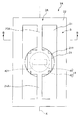
도 1은, 본 발명의 제1 실시 형태에 관한 광 스캐너(액추에이터)를 도시하는 평면도, 도 2는, 도 1 중의 A-A선 단면도, 도 3은, 도 1에 도시하는 광 스캐너에 구비된 가동판을 설명하기 위한 평면도, 도 4는, 도 1 중의 B-B선 단면도, 도 5는, 도 4의 부분 확대 단면도이다. 도 6은, 도 1에 도시하는 광 스캐너의 제조 방법을 설명하는 단면도, 도 7은, 도 1에 도시하는 광 스캐너의 제조 방법을 설명하는 단면도이다. 도 8은, 도 1에 도시하는 광 스캐너의 제조 방법을 설명하는 단면도, 도 9는, 도 8의 (e)에 도시하는 에칭 공정에 있어서의 연결부의 형성(마스크 어긋남이 없는 경우)을 설명하기 위한 도면, 도 10은, 도 8의 (e)에 도시하는 에칭 공정에 있어서의 연결부의 형성(마스크 어긋남이 있는 경우)을 설명하기 위한 도면이다. 또한, 이하에서는, 설명의 편의상, 도 2, 도 4 내지 도 10 중의 상측을 「상」, 하측을 「하」라고 말한다.1 is a plan view showing an optical scanner (actuator) according to a first embodiment of the present invention, FIG. 2 is a cross-sectional view taken along line AA in FIG. 1, and FIG. 3 is a movable plate provided in the optical scanner shown in FIG. 1. 4 is a cross-sectional view taken along line BB of FIG. 1, and FIG. 5 is a partially enlarged cross-sectional view of FIG. 4. 6 is a cross-sectional view illustrating the method of manufacturing the optical scanner shown in FIG. 1, and FIG. 7 is a cross-sectional view illustrating the manufacturing method of the optical scanner shown in FIG. 1. FIG. 8 is a cross-sectional view illustrating the manufacturing method of the optical scanner shown in FIG. 1, and FIG. 9 is a diagram illustrating formation of a connecting portion (when there is no mask misalignment) in an etching step shown in FIG. 8E. FIG. 10: is a figure for demonstrating formation (when there is a mask shift | offset | difference) in the connection part in the etching process shown to FIG. 8E. In addition, below, for convenience of explanation, the upper side in FIG. 2, FIG. 4-FIG. 10 is called "upper | on", and the lower side is called "lower | bottom".
도 1에 도시하는 바와 같이, 광 스캐너(1)는, 진동계를 갖는 기체(2)와, 기체(2)를 지지하는 지지체(3)와, 기체(2)의 진동계를 진동시키는 구동부(4)를 갖는다. As shown in FIG. 1, the
또한, 기체(2)는, 광 반사부(211)가 설치된 가동판(가동부)(21)과, 가동판(21)에 연결하는 한 쌍의 연결부(23, 24)와, 한 쌍의 연결부(23, 24)를 지지하는 지지부(22)를 갖고 있다. 지지부(22)는 연결부(23, 24)를 통해서 가동판(21)을 지지하고 있다고도 말할 수 있고, 한 쌍의 연결부(23, 24)는 가동판(21)과 지지부(22)를 연결하고 있다고도 말할 수 있다.In addition, the
이와 같은 광 스캐너(1)에서는, 구동부(4)의 구동력에 의해, 각 연결부(23, 24)를 비틀림 변형시키면서, 가동판(21)을 연결부(23, 24)에 따른 소정의 축 둘레에 회동시킨다. 이에 의해, 광 반사부(211)에서 반사한 광을 소정의 한 방향으로 주사할 수 있다.In such an
이하, 광 스캐너(1)를 구성하는 각 부를 순차 상세하게 설명한다.Hereinafter, each part which comprises the
[기체][gas]
기체(2)는, 전술한 바와 같이, 광 반사부(211)가 설치된 가동판(21)과, 가동판(21)을 지지하는 지지부(22)와, 가동판(21)과 지지부(22)를 연결하는 한 쌍의 연결부(23, 24)를 갖는다.As described above, the
이와 같은 기체(2)는 실리콘을 주재료로서 구성되어 있고, 가동판(21), 지지부(22) 및 연결부(23, 24)가 일체적으로 형성되어 있다. 보다 구체적으로는, 기체(2)는, 이후에 상세하게 서술하는 바와 같이, 판면이 실리콘의 (100)면으로 구성된 실리콘 기판을 이방성 에칭함으로써 형성된 것이다. 이와 같은 이방성 에칭에 의해, 실리콘의 (111)면을 에칭 정지층으로서 이용해서 간단하고 또한 고정밀도로, 가동판(21), 지지부(22) 및 한 쌍의 연결부(23, 24)를 형성할 수 있다. 또한, 실리콘 기판으로서는, 일반적으로 단결정 실리콘 기판이 사용된다.The
또한, 이와 같은 기체(2)의 상면 및 하면은, 각각, 실리콘의 (100)면으로 구성되어 있다. 또한, 지지부(22)의 내주면, 가동판(21)의 측면 및 각 연결부(23, 24)의 측면의 축선 X에 평행한 부분은, 각각, 실리콘의 (111)면으로 구성되어 있다.In addition, the upper surface and the lower surface of such a
또한, 실리콘은 경량이고 또한 SUS와 같은 정도의 강성을 가지므로, 기체(2)가 실리콘을 주재료로서 구성되어 있음으로써, 우수한 진동 특성을 갖는 기체(2)가 얻어진다. 또한, 실리콘은 후술하는 바와 같이 에칭에 의해 고정밀도인 치수 정밀도로 가공이 가능하므로, 실리콘 기판을 사용해서 기체(2)를 형성함으로써, 원하는 형상(원하는 진동 특성)을 갖는 기체(2)를 얻을 수 있다.In addition, since silicon is light in weight and has rigidity similar to that of SUS, since the
이하, 기체(2)에 대해서 더욱 상세하게 서술한다.Hereinafter, the
지지부(22)는, 도 1에 도시하는 바와 같이, 프레임 형상을 이루고 있다. 보다 구체적으로는, 지지부(22)는 사각 고리 형상을 이루고 있다. 이와 같은 지지부(22)는, 한 쌍의 연결부(23, 24)를 통해서 가동판(21)을 지지한다. 또한, 지지부(22)의 형상으로서는, 한 쌍의 연결부(23, 24)를 통해서 가동판(21)을 지지할 수 있으면, 특별히 한정되지 않고, 예를 들어, 각 연결부(23, 24)에 대응하여 분할된 형상을 이루고 있어도 좋다.The
이와 같은 지지부(22)의 내측에는, 가동판(21)이 설치되어 있다.The
가동판(21)은 판 형상을 이루고 있다. 또한, 본 실시 형태에서는, 가동판(21)은 가동판(21)의 판 두께 방향으로부터의 평면에서 보아, 사각형(본 실시 형태에서는 정사각형)의 4개의 코너부가 각각 결손된 형상(십자 형상)을 이루고 있다. 이에 의해, 가동판(21)의 상면의 광 반사부(211)의 면적(광 반사 영역)을 충분히 확보하면서, 가동판(21)의 회동시의 관성 모멘트를 저감할 수 있다. 또한, 이와 같은 가동판(21)은 이후에 상세하게 서술하는 바와 같이 실리콘 기판을 이방성 에칭함으로써, 간단하고 또한 고정밀도로 형성할 수 있다.The
보다 구체적으로 설명하면, 도 3에 도시하는 바와 같이, 가동판(21)은 본체부(212)와, 이 본체부(212)로부터 축선 X에 평행한 방향으로 양측에 돌출되는 한 쌍의 돌출부(213, 214)와, 본체부(212)로부터 축선 X에 수직인 방향(선분 Y에 평행한 방향)으로 양측에 돌출되는 한 쌍의 돌출부(215, 216)로 구성되어 있다. 이에 의해, 가동판(21)은 판 두께 방향으로부터의 평면에서 보아 십자 형상을 이룬다.More specifically, as shown in FIG. 3, the
그리고, 가동판(21)의 외주에 따른 방향에 있어서의 돌출부(213)와 돌출부(215) 사이에는, 결손부(251)가 형성되어 있다. 또한, 가동판(21)의 외주에 따른 방향에 있어서의 돌출부(213)와 돌출부(216) 사이에는, 결손부(252)가 형성되어 있다. 또한, 가동판(21)의 외주에 따른 방향에 있어서의 돌출부(214)와 돌출부(216) 사이에는, 결손부(254)가 형성되어 있다. 또한, 가동판(21)의 외주에 따른 방향에 있어서의 돌출부(214)와 돌출부(215) 사이에는, 결손부(253)가 형성되어 있다. The missing
바꾸어 말하면, 가동판(21)의 판 두께 방향으로부터의 평면에서 보아, 가동판(21)의 외주에 따라, 결손부(251), 돌출부(213), 결손부(252), 돌출부(216), 결손부(254), 돌출부(214), 결손부(252), 돌출부(215)가 이 순서대로 나란히 설치되어 있다.In other words, in the plane from the plate thickness direction of the
또한, 결손부(251)와 결손부(252)는 돌출부(213)를 통해서 대향하고 있다. 또한, 결손부(252)와 결손부(254)는 돌출부(216)를 통해서 대향하고 있다. 또한, 결손부(253)와 결손부(254)는 돌출부(214)를 통해서 대향하고 있다. 또한, 결손부(251)와 결손부(253)는 돌출부(215)를 통해서 대향하고 있다.In addition, the
이와 같은 돌출부(213 내지 216) 및 결손부(251 내지 254)는, 각각, 가동판(21)의 판 두께 방향으로부터의 평면에서 보아 사각형을 이루고 있다. 또한, 도 1, 도 3에서는, 각 결손부(251 내지 254)의 평면에서 보아 형상이 정사각형을 이루는 상태를 일례로서 도시하고 있다. 가동판(21)의 십자 형상의 외형에 있어서의 코너부에는, 소정의 결정면뿐만 아니라 복수의 결정면이 드러나기 때문에 코너부는 엄밀하게는 직각으로 되지 않고, 각 결손부(251 내지 254)는 엄밀하게는 사각형은 아니다. 그러나, 본 실시 형태에서는, 상기의 상태를 포함시켜 각 결손부(251 내지 254)는 사각형이라고 간주한다.Such protruding
이와 같은 가동판(21)의 판 두께 방향으로부터의 평면에서 보아 외형은, 주로, 가동판(21)의 회동 중심축(축선 X)에 평행한 선분과, 가동판(21)의 회동 중심축(축선 X)에 대해서 수직인 선분(선분 Y)으로 구성되어 있다. 이에 의해, 후술하는 바와 같이 실리콘 기판을 이방성 에칭함으로써, 가동판(21)을 간단하고 또한 고정밀도로 형성할 수 있다. 또한, 가동판(21)의 십자 형상의 외형에 있어서의 코너부에는, 소정의 결정면뿐만 아니라 복수의 결정면이 드러난다. 따라서, 가동판(21)의 판 두께 방향으로부터의 평면에서 보아 코너부의 외형은 축선 X 또는 선분 Y에 반드시 평행한 선분으로 되지 않는다. 즉, 가동판(21)의 판 두께 방향으로부터의 평면에서 보아 외형은, 적어도 상기의 가동판(21)의 코너부를 제외하고, 축선 X에 평행한 선분과 선분 Y에 평행한 선분으로 구성되어 있다.As seen from the plane from the plate | board thickness direction of such a
또한, 가동판(21)은, 평면에서 보아 가동판(21)의 회동 중심축(축선 X)에 대해서 대칭인 형상을 이루고 있다. 이에 의해, 간단하게, 가동판(21)의 무게 중심을 가동판(21)의 회동 중심축 상에 위치시켜, 가동판(21)의 회동을 원활한 것으로 할 수 있다.Moreover, the
또한, 가동판(21)은, 평면에서 보아 가동판(21)의 중심 P를 지나고 또한 가동판(21)의 회동 중심축(축선 X)에 대해서 수직인 선분 Y에 대해서 대칭인 형상을 이루고 있다. 이에 의해, 가동판의 설계가 용이하게 된다.In addition, the
또한, 가동판(21)의 판면은 실리콘의 (100)면으로 구성되어 있다. 이에 의해, 후술하는 바와 같이 판면이 (100)면으로 구성된 실리콘 기판을 이방성 에칭함으로써, 가동판(21), 지지부(22) 및 한 쌍의 연결부(23, 24)를 간단하고 또한 고정밀도로 형성할 수 있다.In addition, the plate surface of the
또한, 가동판(21)의 측면은, 주로, 실리콘의 (111)면으로 구성되어 있다. 이에 의해, 후술하는 바와 같이 판면이 (100)면으로 구성된 실리콘 기판을 이방성 에칭함으로써, 실리콘의 (111)면을 에칭의 정지층으로서 이용하고, 가동판(21), 지지부(22) 및 한 쌍의 연결부(23, 24)를 간단하고 또한 고정밀도로 형성할 수 있다. 또한, 가동판(21)의 판 두께 방향으로부터의 평면에서 보아 외형의 코너부에 있어서는, 가동판(21)의 측면은 (111)면 이외의 결정면을 포함하고 있다. 따라서, 가동판(21)의 측면은, 적어도 그 코너부에 있어서의 측면을 제외하고, 실리콘의 (111)면으로 구성되어 있다.In addition, the side surface of the
또한, 가동판(21)의 측면에는, 횡단면이 V자 형상을 이루는 홈(217)이 형성되어 있다. 이에 의해, 가동판(21)의 관성 모멘트를 저감할 수 있다. 또한, 이와 같은 홈은, 판면이 (100)면으로 구성된 실리콘 기판을 이방성 에칭함으로써, 실리콘의 (111)면을 에칭의 정지층으로서 이용하고, 간단하고 또한 고정밀도로 형성할 수 있다.Moreover, the groove |
또한, 가동판(21)의 판 두께 방향으로부터의 평면에서 보아 회동 중심축(축선 X)에 대해서 수직인 방향(이하, 「선분 Y 방향」이라고도 말함)에서의 길이를 A로 하고, 가동판(21)의 회동 중심축(축선 X)에 평행한 방향(이하, 「축선 X 방향」이라고도 말함)에서의 길이를 B로 하고, 각 결손부(251 내지 254)의 선분 Y 방향에 따른 길이를 a로 하고, 각 결손부(251 내지 254)의 축선 X 방향에 따른 길이를 b로 하였을 때, 하기 수학식 1의 (A), (B)를 각각 충족시킨다.In addition, the length of the

상기 수학식 1의 (A), (B)를 각각 충족시킴으로써, 가동판(21)의 광 반사부(211)의 광 반사에 필요한 면적을 확보하면서, 가동판(21)의 회동시에서의 관성 모멘트를 효율적으로 저감할 수 있다.By satisfying the above formulas (A) and (B), respectively, the inertia at the time of rotation of the
이에 대해, 길이 a, b가 상기 하한값 미만이면, 각각, 가동판(21)의 회동시에서의 관성 모멘트를 저감하는 효과가 작은 경향이 된다. 그로 인해, 가동판(21)의 두께에 따라서는, 가동판(21)의 휘어짐에 따른 이동이 커져, 광 스캐너(1)의 광학 특성을 저하시킬 경우가 있다.On the other hand, when length a, b is less than the said lower limit, the effect of reducing the moment of inertia at the time of rotation of the
한편, 길이 a, b가 상기 상한값을 초과하면, 가동판(21)의 광 반사부(211)의 면적을 효율적으로 사용할 수 없어, 광 반사부(211)에서의 반사광의 강도가 작아지는 경향을 나타낸다.On the other hand, if the lengths a and b exceed the upper limit, the area of the
또한, 도 3에서는, 상기 수학식 1의 (A), (B)를 충족시키고, a, b를 각각 최대로 한 경우의 가동판(21A), a, b를 각각 최소로 한 경우의 가동판(21B)을 각각 쇄선으로 나타내고 있다.In addition, in FIG. 3, the movable plate at the time of satisfying the said Formula (A), (B) of said Formula (1), and making a and b the maximum, respectively, 21 A, and a and b the minimum, respectively. 21B is shown with the chain line, respectively.
이하, 상기 수학식 1의 (A), (B)에 대해서 간단하게 설명한다.Hereinafter, (A) and (B) of
도 3에 도시하는 바와 같이 평면에서 보아 가동판(21)에 광 L의 원형 또는 타원형의 스폿이 내접하는 경우, 각 결손부(251 내지 254)가 광 L의 스폿의 외측에서 면적이 최대가 되는 것은, a=(1-1/√2)A, b=(1-1/√2)B이다.As shown in FIG. 3, when a circular or elliptical spot of light L is inscribed on the
또한, 이러한 경우, 결손부(251 내지 254)를 형성하는 효과가 발휘되는 범위에 있어서, a가 최대가 되고 b가 최소가 되는 것은, 축선 X에 대해서 30° 경사진 선분과 광 L의 스폿의 외주연과의 교점 P2에 각 결손부(251 내지 254)의 코너 P3이 위치할 때이다.In this case, in a range in which the effect of forming the
또한, 이러한 경우, 결손부(251 내지 254)를 형성하는 효과가 발휘되는 범위에 있어서, a가 최소가 되고 b가 최대가 되는 것은, 축선 X에 대해서 60° 경사진 선분과 광 L의 스폿의 외주연과의 교점 P1에 각 결손부(251 내지 254)의 코너 P3이 위치할 때이다.In this case, in a range where the effect of forming the
또한, 광 L로서 통상 사용되는 레이저의 스폿 직경의 유효 범위는, 일반적으로 피크 휘도의 1/e2 이상의 범위가 된다. 따라서, 그 유효 범위가 광 반사부(211) 내에 들어가 있으면, 이상적인 광 반사를 행할 수 있다.In addition, the effective range of the spot diameter of the laser normally used as the light L is generally 1 / e 2 of the peak luminance. It becomes the above range. Therefore, if the effective range is in the
단, 실제의 레이저는, 상기 유효 범위의 외측이어도, 약간의 광이 존재하고, a, b가 상기 값에 대해서 약간 작거나 크거나 해도, 실제 사용상 문제없이 허용할 수 있다.However, even if an actual laser exists outside the said effective range, even if some light exists and a and b are a little small or big with respect to the said value, it can accept without a practical use problem.
구체적으로는, 상세하게 서술한 바와 같이 구한 a, b의 허용값을 -20% 이상 +200% 이하로 할 수 있다.Specifically, the allowable values of a and b obtained as described in detail can be -20% or more and + 200% or less.
이상과 같으므로, 상기 수학식 1의 (A), (B)가 얻어진다.Since it is as above, (A) and (B) of said Formula (1) are obtained.
이와 같은 가동판(21)의 상면에는, 광 반사성을 갖는 광 반사부(211)가 설치되어 있다. 한편, 가동판(21)의 하면에는, 후술하는 구동부(4)의 영구 자석(41)이 설치되어 있다. 또한, 영구 자석(41)에 대해서는, 후술하는 구동부(4)의 설명에 있어서 상세하게 서술한다.On the upper surface of such a
각 연결부(23, 24)는 길이 형상을 이루고 있고, 탄성 변형 가능하게 구성되어 있다. 또한, 연결부(23) 및 연결부(24)는 가동판(21)을 통해서 대향하고 있다. 이와 같은 연결부(23, 24)는, 각각, 가동판(21)을 지지부(22)에 대해서 회동 가능하게 하도록, 가동판(21)과 지지부(22)를 연결되어 있다. 한 쌍의 연결부(23, 24)는, 축선 X에 따라 동축적으로 설치되어 있고, 이 축선 X를 회동 중심축으로서, 가동판(21)이 지지부(22)에 대해서 회동한다.Each
본 실시 형태에서는, 도 1에 도시하는 바와 같이, 연결부(23)는, 한 쌍의 빔 부재(231, 232)로 구성되어 있다. 마찬가지로, 연결부(24)는, 한 쌍의 빔 부재(241, 242)로 구성되어 있다. 이하, 연결부(23)에 대해서 대표적으로 설명하고, 연결부(24)에 대해서는, 연결부(23)와 마찬가지이므로, 그 설명을 생략한다.In this embodiment, as shown in FIG. 1, the
각 빔 부재(231, 232)는, 축선 X에 따라 설치되어 있는 동시에, 축선 X를 통해서 대향하고 있다. 또한, 각 빔 부재(231, 232)는, 그 횡단면 형상이 평행 사변형을 이루고 있다.Each
보다 구체적으로는, 각 빔 부재(231, 232)의 횡단면의 외형은, 각각, 실리콘의 (100) 면에 따른 한 쌍의 변과, 실리콘의 (111) 면에 따른 한 쌍의 변으로 구성된 평행 사변형을 이루고 있다. 즉, 빔 부재(231)는, 상면(2311) 및 하면(2312)이 각각 실리콘의 (100)면으로 구성되고, 한 쌍의 측면(2313, 2314)이 각각 실리콘의 (111)면으로 구성되어 있다. 마찬가지로, 빔 부재(232)는 상면(2321) 및 하면(2322)이 각각 실리콘의 (100)면으로 구성되고, 한 쌍의 측면(2323, 2324)이 각각 실리콘의 (111)면으로 구성되어 있다. 여기서, 측면(2313, 2314, 2323, 2324)은, 각각, 실리콘의 (111)면으로 구성되어 있으므로, 기체(2)의 상면 또는 하면[즉 실리콘의 (100)면]에 대한 경사각 θ가 54.73°가 되어 있다. 이와 같은 횡단면 형상을 이루는 각 빔 부재(231, 232)는, 판면이 실리콘의 (100)면으로 구성된 실리콘 기판을 이방성 에칭함으로써 간단하고 또한 확실하게 형성할 수 있다.More specifically, the shape of the cross section of each
이와 같이 연결부(23)의 외표면이 실리콘의 (100)면 및 (111)면으로 구성되어 있으면, 후술하는 바와 같이 실리콘의 (111)면을 에칭의 정지층으로서 이용하고, 간단하고 또한 고정밀도로 연결부(23)를 형성할 수 있다.Thus, if the outer surface of the
또한, 빔 부재(231, 232)는, 축선 X에 평행한 방향에서 보았을 때에(바꾸어 말하면, 도 5에 도시하는 단면에서 보았을 때), 상하로 연장되고 축선 X를 지나는 선분에 대해서 대칭인 형상을 이루고 있다.The
또한, 도 5에 도시하는 단면에서, 연결부(23) 전체의 폭[빔 부재(231)의 측면(2313)과 빔 부재(232)의 측면(2323)과의 면간 거리]은, 하측으로부터 상측을 향해서 확대되어 있다. 또한, 도 5에 도시하는 단면에서, 빔 부재(231)와 빔 부재(232) 사이의 거리(간극의 폭)는, 하측으로부터 상측을 향해서 확대되어 있다.In addition, in the cross section shown in FIG. 5, the width (interface distance between the
즉, 한 쌍의 빔 부재(231, 232) 사이의 거리는, 가동판(21)의 회동 중심축에 평행한 방향에서 보았을 때에, 가동판(21)의 한쪽의 면측으로부터 다른 쪽의 면측을 향해서(본 실시 형태에서는 하측으로부터 상측을 향해서) 점증하고 있다.That is, when the distance between the pair of
그리고, 한 쌍의 빔 부재(231, 232)의 하측의 단부끼리의 사이의 거리를 W1로 하고, 한 쌍의 빔 부재(231, 232)의 가동판(21)의 두께 방향에서의 두께를 t로 하였을 때, 하기 수학식 2를 충족시킨다.The distance between the lower ends of the pair of

이후에 상세하게 서술하는 바와 같이, 판면이 실리콘의 (100)면으로 구성된 실리콘 기판을 그 양면측으로부터 이방성 에칭하므로, 가동판(21), 지지부(22) 및 한 쌍의 연결부(23, 24)를 형성할 때에, 실리콘 기판의 양면에 형성한 마스크의 형성 위치가 어긋나는 경우가 있다. 이와 같이, 실리콘 기판의 양면 마스크의 형성 위치가 어긋나면, 각 빔 부재(231, 232)의 실리콘의 (111)면으로 구성되어야 할 한 쌍의 측면(2313, 2314, 2323, 2324)에 단차가 생기게 된다. 상기 수학식 2를 충족시킴으로써, 실리콘 기판의 양면에 형성한 마스크의 형성 위치가 어긋난 경우에, 한쪽 측면에 형성된 단차와, 다른 쪽 측면에 형성된 단차를 실리콘 기판의 두께 방향으로 어긋나게 할 수 있다(도 10 참조). 그로 인해, 가동판(21)의 회동시에서의 각 빔 부재(231, 232)에 생기는 응력 집중을 완화시킬 수 있다.As will be described in detail later, since the plate surface is anisotropically etched from the both sides of the silicon substrate composed of the (100) plane of silicon, the
이와 같이 하여, 광 스캐너(1)는 구동시의 응력 집중에 의한 파손을 비교적 간단하게 방지할 수 있다.In this manner, the
또한, 한 쌍의 빔 부재(231, 232)의 상측의 단부끼리의 사이의 거리를 W2로 하였을 때, 하기 수학식 3을 충족시킨다.Further, when the distance between the upper ends of the pair of

이에 의해, 판면이 실리콘의 (100)면으로 구성된 실리콘 기판을 그 양면측으로부터 이방성 에칭함으로써, 한 쌍의 빔 부재(231, 232)로 구성된 연결부(23)를 간단하고 또한 확실하게 형성할 수 있다.Thereby, by anisotropically etching the silicon substrate whose plate surface is comprised from the (100) surface of silicon from the both sides, the
[지지체][Support]
지지체(3)는, 전술한 기체(2)를 지지하는 기능을 갖는다. 또한, 지지체(3)는, 후술하는 구동부(4)의 코일(42)을 지지하는 기능도 갖는다.The
이 지지체(3)는 상방에 개방하는 오목부(31)를 갖는 상자 형상을 이루고 있다. 바꾸어 말하면, 지지체(3)는 판 형상을 이루는 판 형상부(32)와, 그 판 형상부(32)의 상면의 외주부에 따라 설치된 프레임 형상을 이루는 프레임 형상부(33)로 구성되어 있다.This
이와 같은 지지체(3)의 상면 중 오목부(31)의 외측 부분, 즉, 프레임 형상부(33)의 상면에는, 전술한 기체(2)의 지지부(22)의 하면이 접합되어 있다. 이에 의해, 기체(2)의 가동판(21) 및 한 쌍의 연결부(23, 24)와 지지체(3) 사이에는, 가동판(21)의 회동을 허용하는 공간이 형성되어 있다.The lower surface of the
이와 같은 지지체(3)의 구성 재료로서는, 특별히 한정되지 않지만, 예를 들어, 석영 글래스, 파이렉스 글래스(「PYREX」는 등록 상표), TEMPAX 글래스 등의 글래스 재료나, 단결정 실리콘, 폴리 실리콘 등의 실리콘 재료, LTCC(저온 소결 세라믹스) 등을 들 수 있다.Although it does not specifically limit as a constituent material of such a
또한, 기체(2)와 지지체(3)와의 접합 방법으로서는, 지지체(3)의 구성 재료, 형상 등에 따라서 적절하게 결정되는 것이며, 특별히 한정되지 않지만, 접착제를 사용한 방법, 양극 접합법, 직접 접합법 등을 들 수 있다.In addition, as a joining method of the
[구동부][Driving section]
구동부(4)는, 영구 자석(41) 및 코일(42)을 갖고, 전술한 기체(2)의 가동판(21)을 전자 구동 방식(보다 구체적으로는 무빙 마그네트형의 전자 구동 방식)에 의해 회동 구동시키는 것이다. 전자 구동 방식은, 큰 구동력을 발생시킬 수 있다. 그로 인해, 전자 구동 방식을 채용하는 구동부(4)에 따르면, 저구동 전압화를 도모하면서, 가동판(21)의 진동각을 크게 할 수 있다.The
영구 자석(41)은 가동판(21)의 하면에 예를 들어 접착제를 통해서 고정되어 있다. 또한, 영구 자석(41)은 길이 형상을 이루고 있고, 평면에서 보아 축선 X에 대해서 직교하는 방향으로 연장되도록 설치되어 있다. 이와 같은 영구 자석(41)은, 길이 방향으로 자화되어 있고, 길이 방향의 일측이 S극, 타측이 N극이 되어 있다. 영구 자석(41)을 축선 X에 대해서 직교하는 방향으로 연장되도록 설치함으로써, 영구 자석(41)의 양단부를 축선 X로부터 떨어진 부분에 위치시킬 수 있다. 그로 인해, 코일(42)이 발생하는 자계의 작용에 의해, 가동판(21)에 의해 큰 토크를 부여할 수 있다.The
이와 같은 영구 자석(41)으로서는, 특별히 한정되지 않고, 예를 들어, 네오디뮴 자석, 페라이트 자석, 사마륨 코발트 자석, 알니코 자석, 본드 자석 등의, 경자성체를 착자한 것을 적절히 사용할 수 있다.As such a
코일(42)은 지지체(3)의 오목부(31)의 저면(311) 상에 가동판(21)과 대향하도록 설치되어 있다. 이에 의해, 코일(42)이 발생하는 자계를 영구 자석(41)에 효과적으로 작용시킬 수 있다. 이 코일(42)은, 도시하지 않은 전원에 전기적으로 접속되어 있고, 전원으로부터 주기적으로 변화하는 전압(교번 전압, 간헐적인 직류 등)이 인가되도록 되어 있다.The
이와 같은 구동부(4)에 의해, 다음과 같이 가동판(21)이 회동한다.By this
우선, 도시하지 않은 전원에 의해 코일(42)에 예를 들어 교번 전압을 인가한다. 이에 의해, 코일(42)의 상측[가동판(21)측]이 N극, 하측이 S극이 되는 제1 자계와, 코일(42)의 상측이 S극, 하측이 N극이 되는 제2 자계가, 교대로 또한 주기적으로 발생한다.First, for example, an alternating voltage is applied to the
제1 전계에서는, 영구 자석(41)의 N극측이 코일(42)에 끌어 당겨지고, 반대로 S극측이 코일(42)로부터 멀어지도록, 가동판(21)이 축선 X를 중심으로 도 2에서 반시계 방향으로 회동한다(제1 상태). 반대로, 제2 전계에서는, 영구 자석(41)의 S극측이 코일(42)에 끌어 당겨지고, 반대로 N극측이 코일(42)로부터 멀어지도록, 가동판(21)이 축선 X를 중심으로 도 2에서 시계 방향으로 회동한다(제2 상태). 이와 같은 제1 상태와 제2 상태가 교대로 반복되고, 가동판(21)이 축선 X를 중심으로 회동한다.In the first electric field, the
(액추에이터의 제조 방법)(Manufacturing Method of Actuator)
이상과 같은 광 스캐너(1)는, 예를 들어, 다음과 같이 하여 제조할 수 있다. 이하, 본 발명의 액추에이터의 제조 방법의 일례로서, 도 6 내지 도 10에 기초하여, 광 스캐너(1)의 제조 방법을 설명한다. 또한, 도 6 내지 도 8은, 각각, 도 2에 대응하는 단면으로 도시되어 있고, 도 9 및 도 10은, 각각, 도 5에 대응하는 단면으로 도시되어 있다.The
광 스캐너(1)의 제조 방법은, 기체(2)를 형성하는 공정을 갖는다.The manufacturing method of the
기체(2)를 형성하는 공정은, [A] 오목부(218)를 형성하는 공정과, [B] 가동판(21), 지지부(22) 및 한 쌍의 연결부(23, 24)를 형성하는 공정을 포함한다.The process of forming the base |
이하, 각 공정을 순차 상세하게 설명한다.Hereinafter, each process is explained in full detail.
[A] 오목부(218)를 형성하는 공정[A] Process of Forming
-A1--A1-
우선, 도 6의 (a)에 도시하는 바와 같이, 실리콘 기판(102)을 준비한다.First, as shown to Fig.6 (a), the
이 실리콘 기판(102)은, 후술하는 에칭을 거침으로써 기체(2)가 되는 것이다.This
구체적으로는, 실리콘 기판(102)은, 그 주면이 실리콘의 (100)면으로 구성된 것이다.Specifically, the main surface of the
-A2--A2-
다음에, 도 6의 (b)에 도시하는 바와 같이, 실리콘 기판(102)의 상면 상에 질화막(51)을 형성하는 동시에, 실리콘 기판(102) 하면 상에 질화막(52)을 형성한다.Next, as shown in FIG. 6B, the
이 질화막(51, 52)은, 각각, 예를 들어, SiN으로 구성되어 있다.The
또한, 질화막(51, 52)의 형성 방법은, 각각, 특별히 한정되지 않지만, 예를 들어, 플라즈마 CVD 등의 기상 성막법을 사용할 수 있다.In addition, the formation method of the
또한, 질화막(51, 52)의 두께는, 특별히 한정되지 않지만, 0.01㎛ 이상 0.2㎛ 이하 정도이다.In addition, the thickness of the
또한, 질화막(51, 52) 대신에, SiO로 구성된 산화막을 예로 들어 열 산화법에 의해 형성해도 좋다.Instead of the
-A3--A3-
다음에, 도 6의 (c)에 도시하는 바와 같이, 질화막(51) 상에 레지스트막(61)을 형성하고, 도 6의 (d)에 도시하는 바와 같이, 질화막(52) 상에 레지스트막(62)을 형성한다.Next, as shown in FIG. 6C, a resist
이 레지스트막(61, 62)은, 각각, 포지티브형 또는 네거티브형의 레지스트 재료로 구성되어 있다.The resist
-A4--A4-
다음에, 레지스트막(62)을 노광 및 현상함으로써, 레지스트막(62)의 오목부(218)의 형성 영역에 대응한 부분을 제거한다. 이에 의해, 도 6의 (e)에 도시하는 바와 같이, 개구(621)를 갖는 레지스트막(62A)을 얻는다.Next, by exposing and developing the resist
-A5--A5-
다음에, 레지스트막(62A)을 마스크로서 사용하여, 질화막(52)의 일부를 에칭에 의해 제거한다. 이에 의해, 도 6의 (f)에 도시하는 바와 같이, 개구(521)를 갖는 질화막(52A)을 얻는다.Next, part of the
상기 에칭[개구(521)의 형성 방법]으로서는, 특별히 한정되지 않지만, 예를 들어, 반응성 이온 에칭(RIE), CF4를 사용한 드라이 에칭 등을 들 수 있다.Examples of the Method of forming an opening (521) the etching is not particularly limited, for example, reactive ion etching (RIE), and the like can be dry-etched with CF 4.
-A6--A6-
다음에, 레지스트막(61, 62A)을 제거한다. 이에 의해, 도 6의 (g)에 도시하는 바와 같이, 실리콘 기판(102)은, 그 상면이 질화막(51)으로 덮여지고, 하면이 질화막(52A)으로 덮여진 상태가 된다.Next, the resist
레지스트막(61, 62A)의 제거 방법으로서는, 특별히 한정되지 않지만, 예를 들어, 황산에 의한 세정, O2 애싱 등을 들 수 있다.As the method of removing the resist film (61, 62A), is not particularly limited, for example, washing with sulfuric acid, O 2 Ashing and the like.
-A7--A7-
다음에, 질화막(52A)을 마스크로서 사용하여, 실리콘 기판(102)을 에칭한다. 이에 의해, 도 7의 (a)에 도시하는 바와 같이, 오목부(218)를 갖는 실리콘 기판(102A)을 얻는다.Next, the
상기 에칭[오목부(218)의 형성 방법]으로서는, 특별히 한정되지 않지만, 후술하는 가동판(21), 지지부(22) 등의 형성을 위한 에칭과 마찬가지로, 이방성 에칭이 적절히 사용된다.Although it does not specifically limit as said etching (method of forming the recessed part 218), Anisotropic etching is used suitably similarly to the etching for formation of the
이러한 이방성 에칭은, 특별히 한정되지 않지만, 예를 들어, KOH 수용액 등을 사용한 웨트 에칭에 의해 행할 수 있다.Although such anisotropic etching is not specifically limited, For example, it can carry out by wet etching using KOH aqueous solution.
-A8--A8-
다음에, 질화막(51, 52A)을 제거한다. 이에 의해, 도 7의 (b)에 도시하는 바와 같이, 실리콘 기판(102A)의 상면 및 하면이 노출된 상태가 된다.Next, the
질화막(51, 52A)의 제거 방법으로서는, 특별히 한정되지 않지만, 상기 공정 A5와 마찬가지로, 예를 들어, 반응성 이온 에칭(RIE), CF4를 사용한 드라이 에칭 등을 들 수 있다.As the method of removing the nitride film (51, 52A), it is not particularly limited, as in the step A5, for example, reactive ion etching (RIE), and the like can be dry-etched with CF 4.
[B] 가동판(21), 지지부(22) 등을 형성하는 공정[B] Process of Forming
-B1--B1-
다음에, 도 7의 (c)에 도시하는 바와 같이, 실리콘 기판(102A)의 상면 상에 질화막(71)을 형성하는 동시에, 실리콘 기판(102A) 하면 상에 질화막(72)을 형성한다.Next, as shown in FIG. 7C, the
이 질화막(71, 72)은, 각각, 예를 들어, SiN으로 구성되어 있다.These
또한, 질화막(71, 72)의 형성 방법은, 각각, 특별히 한정되지 않지만, 상기 공정 A2와 마찬가지로, 예를 들어, 플라즈마 CVD 등의 기상 성막법을 사용할 수 있다.In addition, although the formation method of the
또한, 질화막(71, 72)의 두께는, 특별히 한정되지 않지만, 0.01㎛ 이상 0.3㎛ 이하 정도이다.In addition, the thickness of the
또한, 질화막(71, 72) 대신에, SiO로 구성된 산화막을 예로 들어 열 산화법에 의해 형성해도 좋다.Instead of the
-B2--B2-
다음에, 도 7의 (d)에 도시하는 바와 같이, 질화막(71) 상에 레지스트막(81)을 형성한다.Next, as shown in FIG. 7D, a resist
이 레지스트막(81)은 포지티브형 또는 네거티브형의 레지스트 재료로 구성되어 있다.The resist
-B3--B3-
다음에, 레지스트막(81)을 노광 및 현상함으로써, 레지스트막(81)의 가동판(21), 지지부(22) 및 한 쌍의 연결부(23, 24)의 형성 영역에 대응한 부분이 잔존하도록, 레지스트막(81)의 일부를 제거한다. 이에 의해, 도 7의 (e)에 도시하는 바와 같이, 개구(811)를 갖는 레지스트막(81A)을 얻는다. 또한, 도 7의 (e)에서는 도시하지 않지만, 레지스트막(81A)에는, 한 쌍의 빔 부재(231, 232)의 상단끼리의 사이의 간극에 대응하여 형성된 개구도 형성되어 있다.Next, by exposing and developing the resist
-B4--B4-
다음에, 레지스트막(81A)을 마스크로서 사용하여, 질화막(71)의 일부를 에칭에 의해 제거한다. 이에 의해, 도 7의 (f)에 도시하는 바와 같이, 개구(711)를 갖는 질화막(71A)을 얻는다. 또한, 도 7의 (f)에서는 도시하지 않지만, 질화막(71A)에는, 한 쌍의 빔 부재(231, 232)의 상단끼리의 사이의 간극에 대응하여 형성된 개구도 형성되어 있다.Next, part of the
상기 에칭[개구(711)의 형성 방법]으로서는, 특별히 한정되지 않지만, 상기 공정 A5와 마찬가지로, 예를 들어, 반응성 이온 에칭(RIE), CF4를 사용한 드라이 에칭 등을 들 수 있다.Examples of the Method of forming an opening (711) the etching is not particularly limited, as in the step A5, for example, reactive ion etching (RIE), and the like can be dry-etched with CF 4.
-B5--B5-
다음에, 레지스트막(81A)을 제거한다. 이에 의해, 도 7의 (g)에 도시하는 바와 같이, 실리콘 기판(102A)은, 그 상면이 질화막(71A)으로 덮여지고, 하면이 질화막(72)으로 덮여진 상태가 된다.Next, the resist
레지스트막(81A)의 제거 방법으로서는, 특별히 한정되지 않지만, 예를 들어, 황산에 의한 세정, O2 애싱 등을 들 수 있다.As the removal of the resist film (81A) method is not particularly limited, for example, washing with sulfuric acid, O 2 Ashing and the like.
-B6--B6-
다음에, 도 8의 (a)에 도시하는 바와 같이, 질화막(72) 상에 레지스트막(82)을 형성한다.Next, as shown in FIG. 8A, a resist
이 레지스트막(82)은 포지티브형 또는 네거티브형의 레지스트 재료로 구성되어 있다.The resist
-B7--B7-
다음에, 레지스트막(82)을 노광 및 현상함으로써, 레지스트막(82)의 가동판(21), 지지부(22) 및 한 쌍의 연결부(23, 24)의 형성 영역에 대응한 부분이 잔존하도록, 레지스트막(82)의 일부를 제거한다. 이에 의해, 도 8의 (b)에 도시하는 바와 같이, 개구(821)를 갖는 레지스트막(82A)을 얻는다. 또한, 도 8의 (b)에서는 도시하지 않지만, 레지스트막(82A)에는, 한 쌍의 빔 부재(231, 232)의 하단끼리의 사이의 간극에 대응하여 형성된 개구도 형성되어 있다.Next, by exposing and developing the resist
-B8--B8-
다음에, 레지스트막(82A)을 마스크로서 사용하여, 질화막(72)의 일부를 에칭에 의해 제거한다. 이에 의해, 도 8의 (c)에 도시하는 바와 같이, 개구(721)를 갖는 질화막(72A)을 얻는다. 또한, 도 8의 (c)에서는 도시하지 않지만, 질화막(72A)에는, 한 쌍의 빔 부재(231, 232)의 하단끼리의 사이의 간극에 대응하여 형성된 개구도 형성되어 있다.Next, using the resist
상기 에칭[개구(721)의 형성 방법]으로서는, 특별히 한정되지 않지만, 상기 공정 A5와 마찬가지로, 예를 들어, 반응성 이온 에칭(RIE), CF4를 사용한 드라이 에칭 등을 들 수 있다.Examples of the Method of forming an opening (721) the etching is not particularly limited, as in the step A5, for example, reactive ion etching (RIE), and the like can be dry-etched with CF 4.
-B9--B9-
다음에, 레지스트막(82A)을 제거한다. 이에 의해, 도 8의 (d)에 도시하는 바와 같이, 실리콘 기판(102A)은, 그 상면이 질화막(71A)으로 덮여지고, 하면이 질화막(72A)으로 덮여진 상태가 된다.Next, the resist
레지스트막(82A)의 제거 방법으로서는, 특별히 한정되지 않지만, 예를 들어, 황산에 의한 세정, O2 애싱 등을 들 수 있다.As the removal of the resist film (82A) method is not particularly limited, for example, washing with sulfuric acid, O 2 Ashing and the like.
-B10--B10-
다음에, 질화막(71A, 72A)을 마스크로서 사용하여, 실리콘 기판(102A)을 이방성 에칭한다. 이에 의해, 도 8의 (e)에 도시하는 바와 같이, 기체(2)를 얻는다. 즉, 본 공정의 이방성 에칭에서는, 제1 마스크인 질화막(72A)과 제2 마스크인 질화막(71A)을 통해서 실리콘 기판(102A)을 그 양면측으로부터 이방성 에칭함으로써, 가동판(21), 지지부(22) 및 한 쌍의 연결부(23, 24)를 형성한다.Next, the
상기 이방성 에칭[기체(2)의 형성 방법]은, 특별히 한정되지 않지만, 예를 들어, KOH 수용액 등을 사용한 웨트 에칭에 의해 행할 수 있다.Although the said anisotropic etching (method of forming the base 2) is not specifically limited, For example, it can be performed by wet etching using KOH aqueous solution etc., for example.
여기서, 이러한 이방성 에칭에 의한 연결부(23)의 형성에 대해서 상세하게 서술한다. 또한, 연결부(24)의 형성에 대해서는, 연결부(23)의 형성과 마찬가지이므로, 그 설명을 생략한다.Here, formation of the
도 9에 도시하는 바와 같이, 마스크(제2 마스크)로서 사용하는 질화막(71A)은 연결부(23)의 빔 부재(231)의 상면의 형성 영역에 대응하여 형성된 부분(712)과, 연결부(23)의 빔 부재(232)의 상면의 형성 영역에 대응하여 형성된 부분(713)을 갖고, 부분(712)과 부분(713) 사이에는, 개구(제2 개구)(714)가 형성되어 있다. 이 개구(714)는, 한 쌍의 빔 부재(231, 232)의 상단끼리의 사이의 간극에 대응하여 형성되어 있다.As shown in FIG. 9, the
또한, 마스크(제1 마스크)로서 사용하는 질화막(72A)은 연결부(23)의 빔 부재(231)의 하면의 형성 영역에 대응하여 형성된 부분(722)과, 연결부(23)의 빔 부재(232)의 하면의 형성 영역에 대응하여 형성된 부분(723)을 갖고, 부분(722)과 부분(723) 사이에는, 개구(724)(제1 개구)가 형성되어 있다. 이 개구(724)는, 한 쌍의 빔 부재(231, 232)의 하단끼리의 사이의 간극에 대응하여 형성되어 있다.In addition, the
여기서, 개구(724)의 폭을 Wm1로 하고, 실리콘 기판(102A)의 두께를 T로 하였을 때에, 하기 수학식 4의 관계를 충족시킨다.Here, when the width of the

이와 같은 관계식을 충족시킴으로써, 제1 마스크인 질화막(72A)과 제2 마스크인 질화막(71A)과의 위치 관계가 어긋나고, 그에 따라, 각 빔 부재(231, 232)의 실리콘의 (111)면으로 구성되어야 할 한 쌍의 측면에 단차가 생겨도, 한쪽 측면에 형성된 단차와, 다른 쪽 측면에 형성된 단차를 실리콘 기판의 두께 방향으로 어긋나게 할 수 있다. 그로 인해, 얻어진 액추에이터에 있어서, 가동판(21)의 회동시에서의 각 빔 부재(231, 232)에 생기는 응력 집중을 완화시킬 수 있다.By satisfying such a relational expression, the positional relationship between the
개구(714)의 폭을 Wm2로 하였을 때, 하기 수학식 5를 충족시킨다.When the width of the

이에 의해, 판면이 실리콘의 (100)면으로 구성된 실리콘 기판(102A)을 그 양면측으로부터 이방성 에칭함으로써, 한 쌍의 빔 부재(231, 232)로 구성된 연결부(23)를 간단하고 또한 확실하게 형성할 수 있다.Thereby, by anisotropically etching the
이하, 본 공정의 이방성 에칭에 있어서의 단차의 발생에 대해서 상세하게 서술한다.Hereinafter, generation | occurrence | production of the level | step difference in the anisotropic etching of this process is explained in full detail.
본 공정에 있어서의 이방성 에칭할 때에, 마스크로서 사용하는 질화막(71A, 72A)의 형성 위치가 어긋나지 않은 경우, 도 9의 (a) 내지 도 9의 (d)에 도시하는 바와 같이, 개구(711, 714)를 통해서 실리콘 기판(102A)의 상면이 에칭되는 동시에, 개구(721, 724)를 통해서 실리콘 기판(102A)의 하면이 에칭되어 가고, 한 쌍의 빔 부재(231, 232)가 형성된다. 이 경우, 개구(714) 및 개구(724)의 폭 방향에서의 중심 위치가 서로 폭 방향으로 일치하고 있으므로, 도 9의 (d)에 도시하는 바와 같이, 각 빔 부재(231, 232)의 각 측면은, 단차가 없는, 실리콘의 (111)면으로 구성된 일정한 경사면이 된다.In the anisotropic etching in this step, when the formation positions of the
한편, 본 공정에 있어서의 이방성 에칭할 때에, 마스크로서 사용하는 질화막(71A, 72A)의 형성 위치가 어긋난 경우, 도 10의 (a) 내지 도 10의 (d)에 도시하는 바와 같이, 개구(711, 714)를 통해서 실리콘 기판(102A)의 상면이 에칭되는 동시에, 개구(721, 724)를 통해서 실리콘 기판(102A)의 하면이 에칭되어 가고, 한 쌍의 빔 부재(231, 232)가 형성된다.On the other hand, in the case of anisotropic etching in this step, when the formation positions of the
이 경우, 개구(714) 및 개구(724)의 폭 방향에서의 중심 위치가 서로 폭 방향으로 다르므로, 도 10의 (d)에 도시하는 바와 같이, 빔 부재(231)의 한쪽 측면에는 단차(2315)가 형성되고, 빔 부재(231)의 다른 쪽 측면에는 단차(2316)가 형성된다. 또한, 이와 마찬가지로, 빔 부재(232)의 한쪽 측면에는 단차(2325)가 형성되고, 빔 부재(232)의 다른 쪽 측면에는 단차(2326)가 형성된다.In this case, since the center positions in the width direction of the
단차(2316)는, 전술한 바와 같이 마스크로서 사용하는 질화막(72A)의 개구(724)의 폭이 상기 수학식 4를 충족시키도록 형성되어 있으므로, 실리콘 기판(102A)의 두께 방향에서의 중앙보다도 질화막(72A) 측(하측)으로 형성된다.Since the
이에 대해, 단차(2315)는 질화막(71A)의 개구(711) 및 질화막(72A)의 개구(721)의 폭은 실리콘 기판(102A)의 두께에 대해서 지나치게 크기 때문에, 실리콘 기판(102A)의 두께 방향에서의 중앙에 형성된다.In contrast, in the
그 때문에, 단차(2315)와 단차(2316)는 실리콘 기판(102A)의 두께 방향에서의 위치가 서로 다르다. 마찬가지로, 단차(2325)와 단차(2326)는 실리콘 기판(102A)의 두께 방향에서의 위치가 서로 다르다.Therefore, the
이와 같이, 단차(2315)와 단차(2316)가 실리콘 기판(102A)의 두께 방향에서의 위치가 다르므로, 가동판(21)의 회동시에 빔 부재(231)의 두께 방향에서의 중앙부에 응력이 집중되는 것을 방지 또는 억제할 수 있다. 마찬가지로, 가동판(21)의 회동시에 빔 부재(232)의 두께 방향에서의 중앙부에 응력이 집중되는 것을 방지 또는 억제할 수 있다. 그 결과, 구동시의 응력 집중에 의한 연결부(23)의 파손을 방지할 수 있다. 마찬가지로, 구동시의 응력 집중에 의한 연결부(24)의 파손을 방지할 수 있다.As described above, since the
가령, 개구(724)의 폭이 상기 수학식 4를 충족시키지 않으면, 단차(2315, 2316, 2325, 2326)는 모두 실리콘 기판(102A)의 두께 방향에서의 중앙의 위치에 형성되게 된다. 즉, 단차(2315, 2316, 2325, 2326)는 서로 실리콘 기판(102A)의 두께 방향에서의 위치가 동일해진다. 그 때문에, 구동시에서의 응력 집중에 의한 파손될 우려가 있다.For example, if the width of the
-B11--B11-
다음에, 질화막(71A, 72A)을 제거한다. 이에 의해, 도 8의 (f)에 도시하는 바와 같이, 기체(2)의 상면 및 하면이 노출된 상태가 된다.Next, the
질화막(71A, 72A)의 제거 방법으로서는, 특별히 한정되지 않지만, 상기 공정 A5와 마찬가지로, 예를 들어, 반응성 이온 에칭(RIE), CF4를 사용한 드라이 에칭, 열 인산에 의한 웨트 프로세스 등을 들 수 있다.The removal method of the
또한, 필요에 따라서, 기체(2)의 코너부를 둥글게 하는 처리를 행한다.Moreover, the process which rounds the corner part of the base |
이러한 처리(라운딩 처리)는, 특별히 한정되지 않지만, 예를 들어, 불산과 질산과 아세트산(또는 물)에 의한 등방성 에칭, 열 처리(감압 하, 1000 내지 1200℃ 정도, H2를 도입한 Ar 분위기 하) 등을 들 수 있다.Such a treatment (rounding treatment) is not particularly limited, but for example, isotropic etching with hydrofluoric acid, nitric acid, and acetic acid (or water), heat treatment (at reduced pressure, about 1000 to 1200 ° C., and an Ar atmosphere in which H 2 is introduced). Ha) and the like.
다음에, 도 8의 (g)에 도시하는 바와 같이, 가동판(21)의 하면에, 접착제를 통해서 영구 자석(41)을 고정한다. 또한, 가동판(21)의 하면에, 접착제를 통해서 경자성체를 고정하고, 그 후, 이 경자성체를 착자함으로써, 영구 자석(41)으로 해도 좋다.Next, as shown in FIG. 8G, the
또한, 가동판(21)의 상면에, 금속막을 형성하고, 광 반사부(211)를 형성한다. 이 금속막의 형성 방법으로서는, 특별히 한정되지 않고, 진공 증착, 스퍼터링(저온 스퍼터링), 이온 플레이팅 등의 건식 도금법, 전해 도금, 무전해 도금 등의 습식 도금법, 용사법, 금속박의 접합 등을 들 수 있다.In addition, a metal film is formed on the upper surface of the
또한, 도시하지 않지만, 지지체(3) 상에 코일(42)을 설치하고, 지지체(3)와 기체(2)를 접합한다.In addition, although not shown in figure, the
이상의 공정에 의해, 광 스캐너(1)가 얻어진다.By the above process, the
이상 설명한 바와 같은 광 스캐너(1)의 제조 방법에 따르면, 상기 수학식 4를 충족시키므로, 얻어진 광 스캐너(1)(액추에이터)에 있어서, 가동판(21)의 회동시에서의 각 빔 부재(231, 232, 241, 242)에 생기는 응력 집중을 완화시킬 수 있다.According to the manufacturing method of the
이상 설명한 바와 같은 제1 실시 형태에 관한 광 스캐너(1)(액추에이터)에 따르면, 가동판(21)이 평면에서 보아 십자 형상을 이루고 있으므로, 가동판(21)의 광 반사 영역을 확보하면서, 가동판(21)의 회동시의 관성 모멘트를 저감할 수 있다.According to the optical scanner 1 (actuator) which concerns on 1st Embodiment described above, since the
또한, 이와 같은 평면에서 보아 형상을 이루는 가동판(21)은, 실리콘 기판을 이방성 에칭함으로써 간단하고 또한 고정밀도로 형성할 수 있다.In addition, the
<제2 실시 형태>≪ Second Embodiment >
다음에, 본 발명의 제2 실시 형태에 대해서 설명한다.Next, a second embodiment of the present invention will be described.
도 11은, 본 발명의 제2 실시 형태에 관한 광 스캐너를 도시하는 평면도, 도 12는, 도 11 중의 B-B선 부분 확대 단면도이다.FIG. 11 is a plan view showing an optical scanner according to a second embodiment of the present invention, and FIG. 12 is a partially enlarged cross-sectional view along the line B-B in FIG.
이하, 제2 실시 형태의 광 스캐너에 대해서, 전술한 실시 형태의 광 스캐너와의 차이점을 중심으로 설명하고, 마찬가지의 사항에 대해서는, 그 설명을 생략한다.Hereinafter, the optical scanner of 2nd Embodiment is demonstrated centering on difference with the optical scanner of embodiment mentioned above, and the description is abbreviate | omitted about the same matter.
제2 실시 형태의 광 스캐너는, 연결부의 횡단면 형상이 다른 것 이외는, 제1 실시 형태의 광 스캐너(1)와 거의 마찬가지이다. 또한, 전술한 실시 형태와 마찬가지의 구성에는, 동일한 부호를 부여하고 있다.The optical scanner of the second embodiment is almost the same as the
본 실시 형태의 광 스캐너(1A)는, 도 11에 도시하는 바와 같이, 진동계를 갖는 기체(2A)를 갖고 있다. 기체(2A)는 가동판(21)과, 지지부(22)와, 가동판(21)을 지지부(22)에 대해서 회전 가능하게 연결하는 한 쌍의 연결부(23A, 24A)를 갖는다.The optical scanner 1A of this embodiment has 2 A of bases which have a vibrometer as shown in FIG. The
이하, 연결부(23)에 대해서 대표적으로 설명하고, 연결부(24)에 대해서는, 연결부(23)와 마찬가지이므로, 그 설명을 생략한다.Hereinafter, the
연결부(23A)는, 축선 X에 따라 설치되어 있다. 또한, 연결부(23A)는, 그 횡단면 형상이 사다리꼴을 이루고 있다.The connecting
보다 구체적으로는, 연결부(23A)는, 축선 X에 평행한 방향에서 보았을 때에(바꾸어 말하면, 도 12에 도시하는 단면에서 보았을 때), 상하로 연장되고 축선 X를 지나는 선분에 대해서 대칭(도 12에서 좌우 대칭)인 형상을 이루고 있다.More specifically, the connecting
또한, 도 12에 도시하는 단면에서, 연결부(23A) 전체의 폭은, 하측으로부터 상측을 향해서 확대되어 있다.In addition, in the cross section shown in FIG. 12, the width | variety of the
또한, 연결부(23A)의 횡단면의 외형은, 실리콘의 (100) 면에 따른 한 쌍의 변과, 실리콘의 (111) 면에 따른 한 쌍의 변으로 구성된 사다리꼴을 이루고 있다. 즉, 연결부(23A)는 상면(233) 및 하면(234)이 각각 실리콘의 (100)면으로 구성되고, 한 쌍의 측면(235, 236)이 각각 실리콘의 (111)면으로 구성되어 있다. 여기서, 측면(235, 236)은, 각각, 상면(233) 또는 하면(234)에 대한 경사각 θ가 54.73°가 되어 있다. 이와 같은 횡단면 형상을 이루는 연결부(23A)는, 전술한 제1 실시 형태의 연결부(23)와 마찬가지로, 판면이 실리콘의 (100)면으로 구성된 실리콘 기판을 이방성 에칭함으로써 간단하고 또한 고정밀도로 형성할 수 있다.Moreover, the external shape of the cross section of the
이상 설명한 바와 같은 제2 실시 형태의 광 스캐너(1A)에 의해서도, 광 반사 영역을 확보하면서 가동판의 회동시의 관성 모멘트를 저감하는 동시에, 가동판의 치수 정밀도를 간단하게 우수한 것으로 할 수 있다.Even with the optical scanner 1A of 2nd Embodiment demonstrated above, while maintaining a light reflection area, the moment of inertia at the time of rotation of a movable plate can be reduced, and the dimensional precision of a movable plate can be made easy simply.
<제3 실시 형태>≪ Third Embodiment >
다음에, 본 발명의 제3 실시 형태에 대해서 설명한다.Next, a third embodiment of the present invention will be described.
도 13은, 본 발명의 제3 실시 형태에 관한 스캐너에 구비된 가동판을 설명하기 위한 평면도이다.It is a top view for demonstrating the movable plate with which the scanner which concerns on 3rd Embodiment of this invention was equipped.
이하, 제3 실시 형태의 광 스캐너에 대해서, 전술한 실시 형태의 광 스캐너와의 차이점을 중심으로 설명하고, 마찬가지의 사항에 대해서는, 그 설명을 생략한다.Hereinafter, the optical scanner of 3rd Embodiment is demonstrated centering on difference with the optical scanner of embodiment mentioned above, and the description is abbreviate | omitted about the same matter.
제3 실시 형태의 광 스캐너는, 가동판의 평면에서 보아 형상이 다른 것 이외는, 제1 실시 형태의 광 스캐너(1)와 거의 마찬가지이다. 또한, 전술한 실시 형태와 마찬가지의 구성에는, 동일한 부호를 부여하고 있다.The optical scanner of the third embodiment is almost the same as the
본 실시 형태의 광 스캐너에 구비된 가동판(21C)은, 도 13에 도시하는 바와 같이, 본체부(212C)와, 이 본체부(212C)로부터 축선 X 방향으로 양측에 돌출되는 한 쌍의 돌출부(213C, 214C)와, 본체부(212)로부터 선분 Y 방향으로 양측에 돌출되는 한 쌍의 돌출부(215C, 216C)로 구성되어 있다. 이에 의해, 가동판(21C)은 평면에서 보아 십자 형상을 이룬다.As shown in FIG. 13, the
그리고, 가동판(21C)의 외주에 따른 방향에 있어서의 돌출부(213C)와 돌출부(215C) 사이에는, 결손부(251C)가 형성되어 있다. 또한, 가동판(21C)의 외주에 따른 방향에 있어서의 돌출부(213C)와 돌출부(216C) 사이에는, 결손부(252C)가 형성되어 있다. 또한, 가동판(21C)의 외주에 따른 방향에 있어서의 돌출부(214C)와 돌출부(216C) 사이에는, 결손부(254C)가 형성되어 있다. 또한, 가동판(21C)의 외주에 따른 방향에 있어서의 돌출부(214C)와 돌출부(215C) 사이에는, 결손부(253C)가 형성되어 있다.And the
본 실시 형태에서는, 가동판(21C)은 판 두께 방향으로부터의 평면에서 보아 축선 X에 대해서 대칭으로 되도록 형성되어 있지만, 그 평면에서 보아 선분 Y에 대해서 비대칭으로 되도록 형성되어 있다. 또한, 이하에서는, 결손부(251C, 253C)에 대해서 대표적으로 설명하지만, 결손부(252C, 254C)에 대해서도 마찬가지이다.In the present embodiment, the
보다 구체적으로 설명하면, 결손부(251)의 선분 Y 방향에 따른 길이를 a1로 하고, 결손부(251C)의 축선 X 방향에 따른 길이를 b1로 하였을 때, a1<b1의 관계를 충족시킨다. 즉, 결손부(251C)는 축선 X 방향에 따른 길이가 선분 Y 방향에 따른 길이보다도 긴 직사각형을 이루고 있다. 이에 의해, 가동판(21C)의 축선 X로부터 원위 단부의 질량을 효율적으로 저감할 수 있다. 그로 인해, 가동판(21C)의 회동시의 관성 모멘트를 효과적으로 억제할 수 있다.More specifically, when the length along the line segment Y direction of the
마찬가지로, 결손부(253C)의 선분 Y 방향에서의 길이를 a3으로 하고, 결손부(253C)의 축선 X 방향에서의 길이를 b3으로 하였을 때, a3<b3의 관계를 충족시킨다. 즉, 결손부(253C)는 축선 X 방향의 길이가 선분 Y 방향에서의 길이보다도 긴 직사각형을 이루고 있다. 이에 의해, 가동판(21C)의 축선 X로부터 원위 단부의 질량을 효율적으로 저감할 수 있다. 그로 인해, 가동판(21C)의 회동시의 관성 모멘트를 효과적으로 억제할 수 있다.Similarly, when the length in the line segment Y direction of the
또한, a1>a3, 또한, b1>b3의 관계를 충족시킨다. 이에 의해, 축선 X 방향에 대해서 경사지게 하여 광을 광 반사부(211)에 입사시키는 경우에, 광 반사 영역을 효율적으로 확보할 수 있다.Moreover, the relationship of a1> a3 and b1> b3 is also satisfied. Thereby, in the case where light is incident on the
또한, 이 가동판(21C)에 있어서도, 가동판(21C)의 평면에서 보아 선분 Y 방향에서의 길이를 A로 하고, 가동판(21C)의 축선 X 방향에서의 길이를 B로 하고, 각 결손부(251C 내지 254C)의 선분 Y 방향에서의 길이를 a로 하고, 각 결손부(251C 내지 254C)의 축선 X 방향에서의 길이를 b로 하였을 때, 상기 수학식 1의 (A), (B)를 각각 충족시킨다.Also in this
이상 설명한 바와 같은 제3 실시 형태의 광 스캐너에 의해서도, 광 반사 영역을 확보하면서 가동판의 회동시의 관성 모멘트를 저감하는 동시에, 가동판의 치수 정밀도를 간단하게 우수한 것으로 할 수 있다.Even with the optical scanner of 3rd Embodiment mentioned above, the moment of inertia at the time of rotation of a movable plate can be reduced, ensuring the light reflection area, and can also easily make the dimensional precision of a movable plate simple.
<제4 실시 형태>≪ Fourth Embodiment &
다음에, 본 발명의 제4 실시 형태에 대해서 설명한다.Next, a fourth embodiment of the present invention will be described.
도 14는, 본 발명의 제4 실시 형태에 관한 스캐너에 구비된 가동판을 설명하기 위한 평면도이다.It is a top view for demonstrating the movable plate with which the scanner which concerns on 4th Embodiment of this invention was equipped.
이하, 제4 실시 형태의 광 스캐너에 대해서, 전술한 실시 형태의 광 스캐너와의 차이점을 중심으로 설명하고, 마찬가지의 사항에 대해서는, 그 설명을 생략한다.Hereinafter, the optical scanner of 4th Embodiment is demonstrated centering on difference with the optical scanner of above-mentioned embodiment, and the description is abbreviate | omitted about the same matter.
제4 실시 형태의 광 스캐너는, 가동판의 평면에서 보아 형상이 다른 것 이외는, 제1 실시 형태의 광 스캐너(1)와 거의 마찬가지이다. 또한, 전술한 실시 형태와 마찬가지의 구성에는, 동일한 부호를 부여하고 있다.The optical scanner of the fourth embodiment is almost the same as the
본 실시 형태의 광 스캐너에 구비된 가동판(21D)은, 도 14에 도시하는 바와 같이, 본체부(212D)와, 이 본체부(212D)로부터 축선 X 방향으로 양측에 돌출되는 한 쌍의 돌출부(213D, 214D)와, 본체부(212)로부터 선분 Y 방향으로 양측에 돌출되는 한 쌍의 돌출부(215D, 216D)로 구성되어 있다. 이에 의해, 가동판(21D)은 평면에서 보아 십자 형상을 이룬다.As shown in FIG. 14, the movable plate 21D included in the optical scanner of the present embodiment includes a
그리고, 가동판(21D)의 외주에 따른 방향에 있어서의 돌출부(213D)와 돌출부(215D) 사이에는, 결손부(251D)가 형성되어 있다. 또한, 가동판(21D)의 외주에 따른 방향에 있어서의 돌출부(213D)와 돌출부(216D) 사이에는, 결손부(252D)가 형성되어 있다. 또한, 가동판(21D)의 외주에 따른 방향에 있어서의 돌출부(214D)와 돌출부(216D) 사이에는, 결손부(254D)가 형성되어 있다. 또한, 가동판(21D)의 외주에 따른 방향에 있어서의 돌출부(214D)와 돌출부(215D) 사이에는, 결손부(253D)가 형성되어 있다.And the
본 실시 형태에서는, 가동판(21D)은, 평면에서 보아 축선 X에 대해서 비대칭으로 되도록 형성되고, 평면에서 보아 선분 Y에 대해서 대칭으로 되도록 형성되어 있다. 또한, 이하에서는, 결손부(251D, 252D)에 대해서 대표적으로 설명하지만, 결손부(253D, 254D)에 대해서도 마찬가지이다.In this embodiment, the movable plate 21D is formed to be asymmetrical about the axis X in plan view, and is formed to be symmetrical with respect to the line segment Y in plan view. In addition, below, although the
보다 구체적으로 설명하면, 결손부(251D)의 선분 Y 방향에서의 길이를 a1로 하고, 결손부(251D)의 축선 X 방향에서의 길이를 b1로 하였을 때, a1<b1의 관계를 충족시킨다. 즉, 결손부(251D)는 축선 X 방향의 길이가 선분 Y 방향에서의 길이보다도 긴 직사각형을 이루고 있다. 이에 의해, 가동판(21D)의 축선 X로부터 원위 단부의 질량을 효율적으로 저감할 수 있다. 그로 인해, 가동판(21D)의 회동시의 관성 모멘트를 효과적으로 억제할 수 있다.More specifically, when the length in the line segment Y direction of the
한편, 결손부(252D)의 선분 Y 방향에서의 길이를 a2로 하고, 결손부(252D)의 축선 X 방향에서의 길이를 b2로 하였을 때, a2>b2의 관계를 충족시킨다. 이에 의해, 결손부(252D)의 평면에서 볼 때의 면적이 결손부(251D)의 평면에서 볼 때의 면적보다 커도, 가동판(21D)의 무게 중심이 축선 X로부터 어긋나는 것을 방지 또는 억제할 수 있다. 그로 인해, 가동판(21D)의 회동을 원활한 것으로 할 수 있다. 또한, 본 실시 형태에서는, a1×b1<a2×b2의 관계를 충족시킨다.On the other hand, when the length in the line segment Y direction of the
또한, 이 가동판(21D)에 있어서도, 가동판(21D)의 평면에서 보아 선분 Y 방향에서의 길이를 A로 하고, 가동판(21D)의 축선 X 방향에서의 길이를 B로 하고, 각 결손부(251D 내지 254D)의 선분 Y 방향에서의 길이를 a로 하고, 각 결손부(251D 내지 254D)의 축선 X 방향에서의 길이를 b로 하였을 때, 상기 수학식 1의 (A), (B)를 각각 충족시킨다.Moreover, also in this movable plate 21D, the length in the line segment Y direction is A, and the length in the axial line X direction of the movable plate 21D is B, and each defect is seen from the plane of the movable plate 21D. When the length in the line segment Y direction of the
이상 설명한 바와 같은 제4 실시 형태의 광 스캐너에 의해서도, 광 반사 영역을 확보하면서 가동판의 회동시의 관성 모멘트를 저감하는 동시에, 가동판의 치수 정밀도를 간단하게 우수한 것으로 할 수 있다.The optical scanner according to the fourth embodiment as described above can reduce the moment of inertia at the time of rotation of the movable plate while securing the light reflecting region, and can easily provide excellent dimensional accuracy of the movable plate.
이상 설명한 바와 같은 광 스캐너는, 예를 들어, 프로젝터, 레이저 프린터, 이미징용 디스플레이, 바코드 리더, 주사형 공초점 현미경 등의 화상 형성 장치에 적절히 적용할 수 있다. 그 결과, 우수한 묘화 특성을 갖는 화상 형성 장치를 제공할 수 있다.The optical scanner described above can be suitably applied to an image forming apparatus such as a projector, a laser printer, an imaging display, a barcode reader, a scanning confocal microscope, and the like. As a result, an image forming apparatus having excellent drawing characteristics can be provided.
(화상 형성 장치)(Image forming apparatus)
여기서, 도 15에 기초하여, 본 발명의 화상 형성 장치의 일례를 설명한다.Here, an example of the image forming apparatus of this invention is demonstrated based on FIG.
도 15는, 본 발명의 화상 형성 장치의 구성의 일례를 나타내는 개략도이다. 또한, 이하에서는, 설명의 편의상, 스크린 SC의 길이 방향을 「횡방향」이라고 하고, 길이 방향으로 직각인 방향을 「종방향」이라고 한다.15 is a schematic view showing an example of the configuration of the image forming apparatus of the present invention. In addition, below, the longitudinal direction of screen SC is called "lateral direction" for convenience of description, and the direction orthogonal to a longitudinal direction is called "vertical direction".
프로젝터(9)는, 레이저 등의 광을 출광하는 광원 장치(91)와, 크로스 다이크로익 프리즘(92)과, 한 쌍의 본 발명의 광 스캐너(93, 94)[예를 들어, 광 스캐너(1)와 마찬가지의 구성의 광 스캐너]와, 고정 미러(95)를 갖고 있다. The projector 9 includes a
광원 장치(91)는 적색광을 출광하는 적색 광원 장치(911)와, 청색광을 출광하는 청색 광원 장치(912)와, 녹색광을 출광하는 녹색 광원 장치(913)를 구비하고 있다.The
크로스 다이크로익 프리즘(92)은, 4개의 직각 프리즘을 접합하여 구성되고, 적색 광원 장치(911), 청색 광원 장치(912), 녹색 광원 장치(913)의 각각으로부터 출광된 광을 합성하는 광학 소자이다.The cross
이와 같은 프로젝터(9)는 적색 광원 장치(911), 청색 광원 장치(912), 녹색 광원 장치(913)의 각각으로부터, 도시하지 않은 호스트 컴퓨터로부터의 화상 정보에 기초하여 출광된 광을 크로스 다이크로익 프리즘(92)에 의해 합성하고, 이 합성된 광이, 광 스캐너(93, 94)에 의해 주사되고, 또한 고정 미러(95)에 의해 반사되어, 스크린 SC 상에서 컬러 화상을 형성하도록 구성되어 있다.Such a projector 9 uses a cross dichro to light emitted from each of the red
여기서, 광 스캐너(93, 94)의 광 주사에 대해서 구체적으로 설명한다.Here, the optical scanning of the
우선, 크로스 다이크로익 프리즘(92)에 의해 합성된 광은, 광 스캐너(93)에 의해 횡방향으로 주사된다(주주사). 그리고, 이 횡방향으로 주사된 광은, 광 스캐너(94)에 의해 또한 종방향으로 주사된다(부주사). 이에 의해, 2차원 컬러 화상을 스크린 SC 상에 형성할 수 있다. 이와 같은 광 스캐너(93, 94)로서 본 발명의 광 스캐너를 사용함으로써, 매우 우수한 묘화 특성을 발휘할 수 있다.First, the light synthesized by the cross
단, 프로젝터(9)로서는, 광 스캐너에 의해 광을 주사하고, 대상물에 화상을 형성하도록 구성되어 있으면, 이에 한정되지 않고, 예를 들어, 고정 미러(95)를 생략해도 좋다.However, as long as the projector 9 is configured to scan light with an optical scanner and form an image on the object, the projector 9 is not limited thereto, and the fixed
이와 같이 구성된 프로젝터(9)에 따르면, 전술한 광 스캐너(1)와 마찬가지의 구성의 광 스캐너(93, 94)를 구비하므로, 저렴하게, 고품위의 화상을 얻을 수 있다.According to the projector 9 configured as described above, since the
이상, 본 발명의 액추에이터, 광 스캐너 및 화상 형성 장치에 대해서, 도시한 실시 형태에 기초하여 설명하였지만, 본 발명은 이에 한정되는 것은 아니다. 예를 들어, 본 발명의 액추에이터, 광 스캐너 및 화상 형성 장치에서는, 각 부의 구성은, 마찬가지의 기능을 발휘하는 임의의 구성의 것으로 치환할 수 있고, 또한, 임의의 구성을 부가할 수도 있다.As mentioned above, although the actuator, the optical scanner, and the image forming apparatus of this invention were demonstrated based on embodiment shown, this invention is not limited to this. For example, in the actuator, the optical scanner, and the image forming apparatus of the present invention, the configuration of each part can be replaced with an arbitrary configuration having the same function, and an optional configuration can be added.
또한, 전술한 실시 형태에서는, 가동판이 평면에서 보아 회동 중심축 및 그에 수직인 선분의 적어도 한쪽에 대해서 대칭인 형상을 이루는 경우를 설명하였지만, 이에 한정되지 않고, 가동판이 평면에서 보아 회동 중심축 및 그에 수직인 선분 중 어느 것에 대해서도 비대칭인 형상을 이루고 있어도 좋다.In addition, in the above-described embodiment, the case in which the movable plate has a symmetrical shape with respect to at least one of the pivotal central axis and the line segment perpendicular thereto is described, but the present invention is not limited thereto. You may form an asymmetrical shape with respect to any of the line segments perpendicular | vertical to it.
또한, 전술한 실시 형태에서는, 본 발명의 액추에이터를 광 스캐너에 적용한 경우를 예로 설명하였지만, 본 발명의 액추에이터는, 이에 한정되지 않고, 예를 들어, 광 스위치, 광 어테뉴에이터 등의 다른 광학 디바이스에 적용하는 것도 가능하다.In addition, in the above-described embodiment, the case where the actuator of the present invention is applied to the optical scanner has been described as an example, but the actuator of the present invention is not limited thereto, and for example, may be applied to another optical device such as an optical switch or an optical attenuator. It is also possible to apply.
또한, 전술한 실시 형태에서는, 가동판을 회동시키는 구동부가 무빙 마그네트형의 전자 구동 방식을 채용한 구성을 예로 설명하였지만, 이러한 구동부는 무빙 코일형의 전자 구동 방식이어도 좋고, 또한, 정전 구동 방식, 압전 구동 방식 등의 전자 구동 방식 이외의 구동 방식을 채용하는 것이어도 좋다.In addition, in the above-described embodiment, the configuration in which the drive unit for rotating the movable plate employs a moving magnet type electron drive method has been described as an example. However, the drive unit may be a moving coil type electron drive method. A drive method other than an electronic drive method such as a piezoelectric drive method may be adopted.
1, 1A : 광 스캐너
2, 2A : 기체
3 : 지지체
4 : 구동부
9 : 프로젝터
21, 21A, 21B, 21C, 21D : 가동판
22 : 지지부
23, 23A : 연결부
24, 24A : 연결부
31 : 오목부
32 : 판 형상부
33 : 프레임 형상부
41 : 영구 자석
42 : 코일
51 : 질화막
52 : 질화막
52A : 질화막
61 : 레지스트막
62 : 레지스트막
62A : 레지스트막
71 : 질화막
71A : 질화막
72 : 질화막
72A : 질화막
81 : 레지스트막
81A : 레지스트막
82 : 레지스트막
82A : 레지스트막
91 : 광원 장치
92 : 크로스 다이크로익 프리즘
93 : 광 스캐너
94 : 광 스캐너
95 : 고정 미러
102 : 실리콘 기판
102A : 실리콘 기판
211 : 광 반사부
212, 212C, 212D : 본체부
213 내지 216, 213C 내지 216C, 213D 내지 216D : 돌출부
217 : 홈
218 : 오목부
231 : 빔 부재
232 : 빔 부재
233 : 상면
234 : 하면
235, 236 : 측면
241 : 빔 부재
242 : 빔 부재
251 내지 254, 251C 내지 254C, 251D 내지 254D : 결손부
311 : 저면
521 : 개구
621 : 개구
711 : 개구
712 : 부분
713 : 부분
714 : 개구
721 : 개구
722 : 부분
723 : 부분
724 : 개구
811 : 개구
821 : 개구
911 : 적색 광원 장치
912 : 청색 광원 장치
913 : 녹색 광원 장치
2311 : 상면
2312 : 하면
2313, 2314 : 측면
2315 : 단차
2316 : 단차
2321 : 상면
2322 : 하면
2323, 2324 : 측면
2325 : 단차
2326 : 단차1, 1A: optical scanner
2, 2A: gas
3: support
4:
9: projector
21, 21A, 21B, 21C, 21D: Moving Plate
22: support
23, 23A: Connection
24, 24A: Connection
31: recess
32: plate shape
33: frame shape
41: permanent magnet
42: Coil
51: nitride film
52: nitride film
52A: Nitride
61: resist film
62: resist film
62A: Resist Film
71: nitride film
71A: Nitride
72: nitride film
72A: Nitride
81: resist film
81A: Resist Film
82: resist film
82A: Resist Film
91: light source device
92: Cross Dichroic Prism
93: optical scanner
94: optical scanner
95: fixed mirror
102: silicon substrate
102A: Silicon Substrate
211: light reflecting unit
212, 212C, 212D: main body
213 to 216, 213C to 216C, 213D to 216D: protrusions
217: home
218: recess
231: beam member
232: beam member
233: upper surface
234: if
235, 236: side
241: beam member
242: beam member
251 to 254, 251C to 254C, 251D to 254D: defective part
311: Bottom
521 opening
621: opening
711 opening
712: part
713: part
714 opening
721 opening
722: part
723: part
724 opening
811 opening
821: opening
911: red light source device
912: blue light source device
913: green light source device
2311: Top
2312: if
2313, 2314: side
2315 step
2316: step
2321: Top
2322: if
2323, 2324: side
2325 step
2326: step
Claims (14)
상기 가동부로부터 연장되고, 또한 상기 가동부의 요동에 따라 비틀림 변형되는 연결부와,
상기 연결부를 지지하는 지지부
를 갖고,
상기 가동부는, 상기 가동부의 두께 방향으로부터의 평면에서 보아 십자 형상을 이루는 것을 특징으로 하는 액추에이터.A movable part swingable around the swing shaft,
A connection portion extending from the movable portion and further twisted and deformed in accordance with the swing of the movable portion;
Support for supporting the connection
Lt; / RTI &
The actuator is characterized by forming a cross shape in plan view from the thickness direction of the movable part.
상기 가동부의 상기 두께 방향으로부터의 평면에서 보아 외형은, 주로, 상기 요동축에 평행한 선분과, 상기 요동축에 대해서 수직인 선분으로 구성되어 있는 액추에이터.The method of claim 1,
An actuator in the form of a plane viewed from the thickness direction of the movable part is mainly composed of a line segment parallel to the oscillation axis and a line segment perpendicular to the oscillation axis.
상기 가동부, 상기 지지부 및 상기 연결부는, 실리콘 기판을 이방성 에칭함으로써 형성된 것인 액추에이터.The method of claim 1,
And the movable portion, the support portion, and the connecting portion are formed by anisotropically etching a silicon substrate.
상기 가동부의 판면은, 실리콘의 (100)면으로 구성되어 있는 액추에이터.The method of claim 3,
The plate surface of the said movable part is an actuator comprised from the (100) surface of silicon.
상기 가동부의 측면은, 주로, 실리콘의 (111)면으로 구성되어 있는 액추에이터.The method of claim 3,
The actuator side surface is mainly comprised by the (111) surface of silicon.
상기 가동부의 측면에는, 상기 가동부의 판면에 직교하는 단면에서 V자 형상을 이루는 홈이 형성되어 있는 액추에이터.The method of claim 5,
An actuator having a groove forming a V-shape in a cross section orthogonal to the plate surface of the movable portion, on the side surface of the movable portion.
상기 연결부의 표면은, 실리콘의 (100)면 및 (111)면으로 구성되어 있는 액추에이터.The method of claim 3,
An actuator surface is formed of (100) and (111) surfaces of silicon.
상기 가동부는, 상기 두께 방향으로부터의 평면에서 보아 상기 가동부의 상기 요동축에 대해서 대칭인 형상을 이루고 있는 액추에이터.The method of claim 1,
And the movable portion has a shape symmetrical with respect to the swing axis of the movable portion in a plan view from the thickness direction.
상기 가동부는, 상기 두께 방향으로부터의 평면에서 보아 상기 가동부의 중심을 지나고 또한 상기 가동부의 상기 요동축에 대해서 수직인 선분에 대해서 대칭인 형상을 이루고 있는 액추에이터.The method of claim 1,
The actuator is formed in a shape symmetrical with respect to a line segment passing through the center of the movable part in a plane from the thickness direction and perpendicular to the oscillation axis of the movable part.
상기 가동부로부터 연장되고, 또한 상기 가동부의 요동에 따라 비틀림 변형되는 연결부와,
상기 연결부를 지지하는 지지부
를 갖고,
상기 가동부는, 상기 가동부의 두께 방향으로부터의 평면에서 보아 사각형의 4개의 코너 부분이 각각 구형(矩形)으로 결손된 형상을 이루는 것을 특징으로 하는 액추에이터.A movable part swingable around the swing shaft,
A connection portion extending from the movable portion and further twisted and deformed in accordance with the swing of the movable portion;
Support for supporting the connection
Lt; / RTI &
The actuator is characterized in that the four corner portions of the quadrangle are formed in a spherical shape in a plan view from the thickness direction of the movable part.
상기 가동부로부터 연장되고, 또한 상기 가동부의 요동에 따라 비틀림 변형되는 연결부와,
상기 연결부를 지지하는 지지부
를 갖고,
상기 가동부는, 상기 가동부의 두께 방향으로부터의 평면에서 보아 십자 형상을 이루는 것을 특징으로 하는 광 스캐너.A movable portion having a light reflecting portion having light reflectivity and capable of oscillating around a swing shaft;
A connection portion extending from the movable portion and further twisted and deformed in accordance with the swing of the movable portion;
Support for supporting the connection
Lt; / RTI &
And the movable portion has a cross shape when viewed in a plane from the thickness direction of the movable portion.
상기 가동부로부터 연장되고, 또한 상기 가동부의 요동에 따라 비틀림 변형되는 연결부와,
상기 연결부를 지지하는 지지부
를 갖고,
상기 가동부는, 상기 가동부의 두께 방향으로부터의 평면에서 보아 사각형의 4개의 코너 부분이 각각 구형으로 결손된 형상을 이루는 것을 특징으로 하는 광 스캐너.A movable portion having a light reflecting portion having light reflectivity and capable of oscillating around a swing shaft;
A connection portion extending from the movable portion and further twisted and deformed in accordance with the swing of the movable portion;
Support for supporting the connection
Lt; / RTI &
And the movable portion has a shape in which four corner portions of a quadrangle are each formed in a spherical shape in a plane from the thickness direction of the movable portion.
상기 광원으로부터의 광을 주사하는 광 스캐너
를 구비하고,
상기 광 스캐너는,
광 반사성을 갖는 광 반사부를 구비하고, 또한 요동축 둘레에 요동 가능한 가동부와,
상기 가동부로부터 연장되고, 또한 상기 가동부의 요동에 따라 비틀림 변형되는 연결부와,
상기 연결부를 지지하는 지지부
를 갖고,
상기 가동부는, 상기 가동부의 두께 방향으로부터의 평면에서 보아 십자 형상을 이루는 것을 특징으로 하는 화상 형성 장치.A light source for emitting light,
An optical scanner for scanning light from the light source
And,
The optical scanner,
A movable portion having a light reflecting portion having light reflectivity and capable of oscillating around a swing shaft;
A connection portion extending from the movable portion and further twisted and deformed in accordance with the swing of the movable portion;
Support for supporting the connection
Lt; / RTI &
And the movable portion has a cross shape when viewed in a plane from the thickness direction of the movable portion.
상기 광원으로부터의 광을 주사하는 광 스캐너
를 구비하고,
상기 광 스캐너는,
광 반사성을 갖는 광 반사부를 구비하고, 또한 요동축 둘레에 요동 가능한 가동부와,
상기 가동부로부터 연장되고, 또한 상기 가동부의 요동에 따라 비틀림 변형되는 연결부와,
상기 연결부를 지지하는 지지부
를 갖고,
상기 가동부는, 상기 가동부의 두께 방향으로부터의 평면에서 보아 사각형의 4개의 코너 부분이 각각 구형으로 결손된 형상을 이루는 것을 특징으로 하는 화상 형성 장치.A light source for emitting light,
An optical scanner for scanning light from the light source
And,
The optical scanner,
A movable portion having a light reflecting portion having light reflectivity and capable of oscillating around a swing shaft;
A connection portion extending from the movable portion and further twisted and deformed in accordance with the swing of the movable portion;
Support for supporting the connection
Lt; / RTI &
And the movable portion forms a shape in which four corner portions of a quadrangle are each formed in a spherical shape in a plane from the thickness direction of the movable portion.
Applications Claiming Priority (3)
| Application Number | Priority Date | Filing Date | Title |
|---|---|---|---|
| JPJP-P-2011-066803 | 2011-03-24 | ||
| JP2011066803A JP5842356B2 (en) | 2011-03-24 | 2011-03-24 | Actuator, optical scanner and image forming apparatus |
| PCT/JP2012/001941 WO2012127858A1 (en) | 2011-03-24 | 2012-03-21 | Actuator, optical scanner, and image generator |
Related Child Applications (1)
| Application Number | Title | Priority Date | Filing Date |
|---|---|---|---|
| KR1020157020253A Division KR20150091423A (en) | 2011-03-24 | 2012-03-21 | Actuator, optical scanner, and image generator |
Publications (1)
| Publication Number | Publication Date |
|---|---|
| KR20130136548A true KR20130136548A (en) | 2013-12-12 |
Family
ID=46877143
Family Applications (2)
| Application Number | Title | Priority Date | Filing Date |
|---|---|---|---|
| KR1020137027783A KR20130136548A (en) | 2011-03-24 | 2012-03-21 | Actuator, optical scanner, and image generator |
| KR1020157020253A KR20150091423A (en) | 2011-03-24 | 2012-03-21 | Actuator, optical scanner, and image generator |
Family Applications After (1)
| Application Number | Title | Priority Date | Filing Date |
|---|---|---|---|
| KR1020157020253A KR20150091423A (en) | 2011-03-24 | 2012-03-21 | Actuator, optical scanner, and image generator |
Country Status (9)
| Country | Link |
|---|---|
| US (1) | US9293975B2 (en) |
| EP (1) | EP2690764A4 (en) |
| JP (1) | JP5842356B2 (en) |
| KR (2) | KR20130136548A (en) |
| CN (1) | CN103430434B (en) |
| BR (1) | BR112013028358A2 (en) |
| RU (1) | RU2566738C2 (en) |
| TW (1) | TWI563290B (en) |
| WO (1) | WO2012127858A1 (en) |
Families Citing this family (12)
| Publication number | Priority date | Publication date | Assignee | Title |
|---|---|---|---|---|
| JP5909862B2 (en) * | 2011-04-06 | 2016-04-27 | セイコーエプソン株式会社 | Actuator, optical scanner and image forming apparatus |
| JP6330321B2 (en) * | 2013-12-26 | 2018-05-30 | セイコーエプソン株式会社 | Optical scanner, image display device, and head mounted display |
| JP6349851B2 (en) * | 2014-03-27 | 2018-07-04 | セイコーエプソン株式会社 | Optical device and image display apparatus |
| JP6565459B2 (en) * | 2015-08-06 | 2019-08-28 | セイコーエプソン株式会社 | Optical scanner, image display device, and head mounted display |
| US11187872B2 (en) | 2017-07-06 | 2021-11-30 | Hamamatsu Photonics K.K. | Optical device |
| US11635613B2 (en) | 2017-07-06 | 2023-04-25 | Hamamatsu Photonics K.K. | Optical device |
| EP3650911B1 (en) | 2017-07-06 | 2023-08-30 | Hamamatsu Photonics K.K. | Optical device |
| JP7112876B2 (en) | 2017-07-06 | 2022-08-04 | 浜松ホトニクス株式会社 | optical device |
| EP4160295A1 (en) | 2017-11-15 | 2023-04-05 | Hamamatsu Photonics K.K. | Optical device production method |
| US11931776B2 (en) | 2018-12-26 | 2024-03-19 | Industrial Technology Research Institute | Actuator, method for manufacturing the actuator, and acoustic transmitter |
| TWI681188B (en) * | 2018-12-26 | 2020-01-01 | 財團法人工業技術研究院 | Actuator and manufacuring method thereof and acoustic transmitter |
| CN111365621B (en) * | 2018-12-26 | 2022-01-11 | 财团法人工业技术研究院 | Actuator and its manufacturing method and sonic wave transmitter |
Family Cites Families (19)
| Publication number | Priority date | Publication date | Assignee | Title |
|---|---|---|---|---|
| DE69102590T2 (en) * | 1990-05-18 | 1994-10-06 | British Aerospace | Inertial sensors. |
| US6831765B2 (en) * | 2001-02-22 | 2004-12-14 | Canon Kabushiki Kaisha | Tiltable-body apparatus, and method of fabricating the same |
| JP3740444B2 (en) * | 2001-07-11 | 2006-02-01 | キヤノン株式会社 | Optical deflector, optical equipment using the same, torsional oscillator |
| JP3919616B2 (en) * | 2002-07-05 | 2007-05-30 | キヤノン株式会社 | Micro structure and manufacturing method thereof |
| JP4641378B2 (en) | 2004-02-16 | 2011-03-02 | キヤノン株式会社 | Optical scanning device and image display device having the same |
| RU41220U1 (en) * | 2004-05-28 | 2004-10-10 | Константинов Станислав Вячеславович | SCANNER |
| WO2005119309A1 (en) | 2004-06-04 | 2005-12-15 | Brother Kogyo Kabushiki Kaisha | Method of producing reflection mirror and reflection mirror |
| JP4645067B2 (en) * | 2004-06-04 | 2011-03-09 | ブラザー工業株式会社 | Reflection mirror manufacturing method |
| JP4193817B2 (en) | 2005-06-22 | 2008-12-10 | セイコーエプソン株式会社 | Actuator |
| JP2009069675A (en) * | 2007-09-14 | 2009-04-02 | Ricoh Co Ltd | Optical scanner, optical scanning device, image forming apparatus and method of manufacturing optical scanner |
| JP5252872B2 (en) | 2007-09-28 | 2013-07-31 | 日本信号株式会社 | Planar type electromagnetic actuator |
| JP2009148847A (en) | 2007-12-19 | 2009-07-09 | Canon Inc | Manufacturing method for structure by anisotropic etching and silicon substrate with etching mask |
| JP2009217193A (en) * | 2008-03-13 | 2009-09-24 | Seiko Epson Corp | Optical deflector and method of manufacturing the same |
| JP5521359B2 (en) * | 2008-03-13 | 2014-06-11 | セイコーエプソン株式会社 | Optical deflector and manufacturing method thereof |
| JP2011170370A (en) | 2008-03-13 | 2011-09-01 | Seiko Epson Corp | Optical deflector and method of manufacturing the same |
| JP2009294458A (en) * | 2008-06-05 | 2009-12-17 | Brother Ind Ltd | Optical scanner |
| JP5655365B2 (en) * | 2009-08-04 | 2015-01-21 | セイコーエプソン株式会社 | Optical deflector, optical deflector manufacturing method, and image display apparatus |
| JP2011107675A (en) | 2009-10-20 | 2011-06-02 | Seiko Epson Corp | Light deflecting element, light deflector and image forming device |
| JP2012220641A (en) * | 2011-04-06 | 2012-11-12 | Seiko Epson Corp | Actuator, optical scanner and image forming device |
-
2011
- 2011-03-24 JP JP2011066803A patent/JP5842356B2/en active Active
-
2012
- 2012-03-05 US US13/411,934 patent/US9293975B2/en active Active
- 2012-03-20 TW TW101109563A patent/TWI563290B/en active
- 2012-03-21 RU RU2013147403/07A patent/RU2566738C2/en not_active IP Right Cessation
- 2012-03-21 KR KR1020137027783A patent/KR20130136548A/en active IP Right Grant
- 2012-03-21 WO PCT/JP2012/001941 patent/WO2012127858A1/en active Application Filing
- 2012-03-21 CN CN201280014388.XA patent/CN103430434B/en active Active
- 2012-03-21 KR KR1020157020253A patent/KR20150091423A/en not_active Application Discontinuation
- 2012-03-21 EP EP12760169.8A patent/EP2690764A4/en not_active Withdrawn
- 2012-03-21 BR BR112013028358A patent/BR112013028358A2/en not_active Application Discontinuation
Also Published As
| Publication number | Publication date |
|---|---|
| KR20150091423A (en) | 2015-08-10 |
| TWI563290B (en) | 2016-12-21 |
| EP2690764A4 (en) | 2016-03-02 |
| TW201239393A (en) | 2012-10-01 |
| JP5842356B2 (en) | 2016-01-13 |
| RU2566738C2 (en) | 2015-10-27 |
| EP2690764A1 (en) | 2014-01-29 |
| JP2012203149A (en) | 2012-10-22 |
| BR112013028358A2 (en) | 2017-01-24 |
| US9293975B2 (en) | 2016-03-22 |
| CN103430434A (en) | 2013-12-04 |
| WO2012127858A1 (en) | 2012-09-27 |
| US20120243066A1 (en) | 2012-09-27 |
| CN103430434B (en) | 2016-08-10 |
| RU2013147403A (en) | 2015-04-27 |
Similar Documents
| Publication | Publication Date | Title |
|---|---|---|
| KR20130136548A (en) | Actuator, optical scanner, and image generator | |
| US9343946B2 (en) | Actuator, optical scanner, and image forming apparatus | |
| JP5909862B2 (en) | Actuator, optical scanner and image forming apparatus | |
| US8988750B2 (en) | Optical scanner, mirror chip, method of manufacturing optical scanner, and image forming apparatus | |
| JP2005128147A (en) | Optical deflector and optical apparatus using the same | |
| JP5333286B2 (en) | Optical scanner and image forming apparatus | |
| JP2009128463A (en) | Method of manufacturing oscillating body apparatus, optical deflector composed of oscillating body apparatus manufactured by the method and optical equipment | |
| JP5640687B2 (en) | Actuator, actuator manufacturing method, optical scanner, and image forming apparatus | |
| JP2012192494A (en) | Actuator, method for manufacturing actuator, optical scanner and image forming apparatus | |
| JP5817158B2 (en) | Optical device, optical device manufacturing method, optical scanner, and image forming apparatus | |
| JP2012123117A (en) | Actuator, optical scanner and image forming device | |
| US8614831B2 (en) | Actuator and optical scanner | |
| JP6003025B2 (en) | Actuator, optical scanner and image forming apparatus | |
| JP5842837B2 (en) | Actuator, optical scanner and image forming apparatus | |
| JP5909914B2 (en) | Actuator, optical scanner and image forming apparatus | |
| JP5354162B2 (en) | Optical device, optical scanner, and image forming apparatus | |
| JP5624638B2 (en) | Silicon processing method and silicon substrate with etching mask | |
| JP2011048229A (en) | Optical scanner and image forming apparatus | |
| JP5168735B2 (en) | Optical device, optical scanner, and image forming apparatus |
Legal Events
| Date | Code | Title | Description |
|---|---|---|---|
| A201 | Request for examination | ||
| E902 | Notification of reason for refusal | ||
| AMND | Amendment | ||
| E601 | Decision to refuse application | ||
| AMND | Amendment | ||
| E801 | Decision on dismissal of amendment | ||
| A107 | Divisional application of patent | ||
| J201 | Request for trial against refusal decision | ||
| J301 | Trial decision |
Free format text: TRIAL NUMBER: 2015101004245; TRIAL DECISION FOR APPEAL AGAINST DECISION TO DECLINE REFUSAL REQUESTED 20150724 Effective date: 20161117 |
|
| S901 | Examination by remand of revocation | ||
| GRNO | Decision to grant (after opposition) |