JP2012220641A - Actuator, optical scanner and image forming device - Google Patents
Actuator, optical scanner and image forming device Download PDFInfo
- Publication number
- JP2012220641A JP2012220641A JP2011084841A JP2011084841A JP2012220641A JP 2012220641 A JP2012220641 A JP 2012220641A JP 2011084841 A JP2011084841 A JP 2011084841A JP 2011084841 A JP2011084841 A JP 2011084841A JP 2012220641 A JP2012220641 A JP 2012220641A
- Authority
- JP
- Japan
- Prior art keywords
- center axis
- plan
- view
- rotation center
- movable plate
- Prior art date
- Legal status (The legal status is an assumption and is not a legal conclusion. Google has not performed a legal analysis and makes no representation as to the accuracy of the status listed.)
- Withdrawn
Links
Images


Classifications
-
- H—ELECTRICITY
- H02—GENERATION; CONVERSION OR DISTRIBUTION OF ELECTRIC POWER
- H02K—DYNAMO-ELECTRIC MACHINES
- H02K33/00—Motors with reciprocating, oscillating or vibrating magnet, armature or coil system
- H02K33/16—Motors with reciprocating, oscillating or vibrating magnet, armature or coil system with polarised armatures moving in alternate directions by reversal or energisation of a single coil system
-
- G—PHYSICS
- G02—OPTICS
- G02B—OPTICAL ELEMENTS, SYSTEMS OR APPARATUS
- G02B26/00—Optical devices or arrangements for the control of light using movable or deformable optical elements
- G02B26/08—Optical devices or arrangements for the control of light using movable or deformable optical elements for controlling the direction of light
- G02B26/0816—Optical devices or arrangements for the control of light using movable or deformable optical elements for controlling the direction of light by means of one or more reflecting elements
- G02B26/0833—Optical devices or arrangements for the control of light using movable or deformable optical elements for controlling the direction of light by means of one or more reflecting elements the reflecting element being a micromechanical device, e.g. a MEMS mirror, DMD
- G02B26/085—Optical devices or arrangements for the control of light using movable or deformable optical elements for controlling the direction of light by means of one or more reflecting elements the reflecting element being a micromechanical device, e.g. a MEMS mirror, DMD the reflecting means being moved or deformed by electromagnetic means
-
- H—ELECTRICITY
- H04—ELECTRIC COMMUNICATION TECHNIQUE
- H04N—PICTORIAL COMMUNICATION, e.g. TELEVISION
- H04N1/00—Scanning, transmission or reproduction of documents or the like, e.g. facsimile transmission; Details thereof
- H04N1/04—Scanning arrangements, i.e. arrangements for the displacement of active reading or reproducing elements relative to the original or reproducing medium, or vice versa
- H04N1/113—Scanning arrangements, i.e. arrangements for the displacement of active reading or reproducing elements relative to the original or reproducing medium, or vice versa using oscillating or rotating mirrors
-
- Y—GENERAL TAGGING OF NEW TECHNOLOGICAL DEVELOPMENTS; GENERAL TAGGING OF CROSS-SECTIONAL TECHNOLOGIES SPANNING OVER SEVERAL SECTIONS OF THE IPC; TECHNICAL SUBJECTS COVERED BY FORMER USPC CROSS-REFERENCE ART COLLECTIONS [XRACs] AND DIGESTS
- Y10—TECHNICAL SUBJECTS COVERED BY FORMER USPC
- Y10T—TECHNICAL SUBJECTS COVERED BY FORMER US CLASSIFICATION
- Y10T74/00—Machine element or mechanism
- Y10T74/18—Mechanical movements
- Y10T74/18568—Reciprocating or oscillating to or from alternating rotary
Landscapes
- Physics & Mathematics (AREA)
- Engineering & Computer Science (AREA)
- Power Engineering (AREA)
- Electromagnetism (AREA)
- General Physics & Mathematics (AREA)
- Optics & Photonics (AREA)
- Micromachines (AREA)
- Mechanical Optical Scanning Systems (AREA)
Abstract
Description
本発明は、アクチュエーター、光スキャナーおよび画像形成装置に関する。 The present invention relates to an actuator, an optical scanner, and an image forming apparatus.
アクチュエーターとしては、捩り振動子を用いたものが知られている(例えば、特許文献1参照)。
例えば、特許文献1には、可動板(可動部)と、支持枠(支持部)と、可動板を支持枠に対して捩り回動可能に支持する1対の弾性支持部(連結部)とを有し、各弾性支持部が2本の棒(梁部材)で構成された光偏向器が開示されている。
As an actuator, one using a torsional vibrator is known (for example, see Patent Document 1).
For example,
このような可動板、支持枠および1対の弾性支持部は、主面がシリコンの(100)面で構成されたシリコン基板を異方性エッチングすることにより一体形成される。
また、特許文献1に係る光偏向器では、可動板が平面視にて八角形をなしている。このような平面視形状をなす可動板は、回動軸から離れた位置での可動板の重量を小さくし、慣性モーメントを低減できるという利点がある。
しかし、平面視形状が八角形をなす可動板は、前述したような異方性エッチングを用いて製造した場合、結晶面との関係から、形状のばらつきが大きくなる。
Such a movable plate, a support frame, and a pair of elastic support portions are integrally formed by anisotropically etching a silicon substrate whose main surface is a (100) surface of silicon.
Moreover, in the optical deflector according to
However, when the movable plate having an octagonal shape in plan view is manufactured using the anisotropic etching as described above, the variation in shape increases due to the relationship with the crystal plane.
本発明の目的は、製造における可動部の形状ばらつきを従来よりも小さくして、可動部の回動時の慣性モーメントを低減することができるアクチュエーター、光スキャナーおよび画像形成装置を提供することにある。 An object of the present invention is to provide an actuator, an optical scanner, and an image forming apparatus that can reduce the variation in the shape of the movable part in manufacturing compared to the conventional art and reduce the moment of inertia when the movable part rotates. .
このような目的は、下記の本発明により達成される。
本発明のアクチュエーターは、所定の回動中心軸まわりに回動可能な板状の可動部と、
前記可動部に連結し、かつ前記可動部の回動に伴って捩り変形する連結部と、
前記連結部を支持する支持部と、を有し、
前記可動部は、前記可動部の板厚方向からの平面視にて、前記回動中心軸に対して垂直な方向で両側へ突出する1対の第1突出部と、前記回動中心軸に対して平行な方向で両側に突出する1対の第2突出部とを有する十字状をなし、
前記板厚方向からの平面視における前記回動中心軸に対して垂直な方向の前記可動部の長さをAとし、前記板厚方向からの平面視における前記回動中心軸に対して平行な方向の前記可動部の長さをBとし、前記板厚方向からの平面視における前記回動中心軸に対して垂直な方向の前記第1突出部の長さをaとし、前記板厚方向からの平面視における前記回動中心軸に対して平行な方向の前記第2突出部の長さをbとしたときに、下記式(A)および(B)をそれぞれ満たすことを特徴とする。

The actuator of the present invention includes a plate-like movable portion that can rotate around a predetermined rotation center axis,
A connecting portion connected to the movable portion and torsionally deformed with the rotation of the movable portion;
A support part for supporting the connecting part,
The movable part includes a pair of first projecting parts projecting to both sides in a direction perpendicular to the pivot center axis in plan view from the plate thickness direction of the movable part, and the pivot center axis. A cross having a pair of second protrusions projecting on both sides in a parallel direction;
The length of the movable portion in a direction perpendicular to the rotation center axis in plan view from the plate thickness direction is A, and is parallel to the rotation center axis in plan view from the plate thickness direction. The length of the movable portion in the direction is B, the length of the first protrusion in the direction perpendicular to the rotation center axis in plan view from the plate thickness direction is a, and from the plate thickness direction The following formulas (A) and (B) are satisfied, where b is the length of the second protrusion in the direction parallel to the rotation center axis in plan view:
本発明のアクチュエーターでは、前記可動部は、a≦bの関係を満たすことが好ましい。
これにより、可動板の回動時の慣性モーメントを効果的に低減することができる。
本発明のアクチュエーターでは、下記式(C)および(D)を満たすことが好ましい。
Thereby, the inertia moment at the time of rotation of a movable plate can be reduced effectively.
In the actuator of the present invention, it is preferable to satisfy the following formulas (C) and (D).
本発明のアクチュエーターでは、前記板厚方向からの平面視における前記可動部の外形は、主として、前記可動部の回動中心軸に平行な線分と、前記可動部の回動中心軸に対して垂直な線分とで構成されていることが好ましい。
これにより、製造における可動部の形状ばらつきを小さくすることができる。
本発明のアクチュエーターでは、前記可動部、前記支持部および前記連結部は、シリコン基板を異方性エッチングすることにより形成されたものであることが好ましい。
これにより、形状ばらつきを小さくして、可動部、支持部および連結部を容易に形成することができる。
In the actuator of the present invention, the outer shape of the movable part in a plan view from the plate thickness direction is mainly with respect to a line segment parallel to the rotation center axis of the movable part and the rotation center axis of the movable part. It is preferably composed of vertical line segments.
Thereby, the shape dispersion | variation of the movable part in manufacture can be made small.
In the actuator according to the aspect of the invention, it is preferable that the movable portion, the support portion, and the connection portion are formed by anisotropic etching of a silicon substrate.
Thereby, shape variation can be made small and a movable part, a support part, and a connection part can be formed easily.
本発明のアクチュエーターでは、前記可動部の板面は、シリコンの(100)面で構成されていることが好ましい。
これにより、板面が(100)面で構成されたシリコン基板を異方性エッチングすることにより、形状ばらつきを小さくして、可動部、支持部および連結部を容易に形成することができる。
In the actuator according to the aspect of the invention, it is preferable that the plate surface of the movable portion is composed of a (100) surface of silicon.
Thereby, by anisotropically etching a silicon substrate having a (100) plane, the shape variation can be reduced, and the movable portion, the support portion, and the connecting portion can be easily formed.
本発明のアクチュエーターでは、前記可動部の側面は、主として、シリコンの(111)面で構成されていることが好ましい。
これにより、板面が(100)面で構成されたシリコン基板を異方性エッチングすることにより、シリコンの(111)面をエッチングの停止層として利用し、形状ばらつきを小さくして、可動部、支持部および連結部を容易に形成することができる。
In the actuator according to the aspect of the invention, it is preferable that the side surface of the movable part is mainly composed of a (111) surface of silicon.
Thus, by anisotropically etching a silicon substrate having a (100) plane as a plate surface, the (111) plane of silicon is used as an etching stop layer, and the shape variation is reduced. A support part and a connection part can be formed easily.
本発明のアクチュエーターでは、前記可動部の側面には、前記可動部の板面に直交する断面においてV字状をなす溝が形成されていることが好ましい。
これにより、可動部の慣性モーメントを低減することができる。また、このような溝は、板面が(100)面で構成されたシリコン基板を異方性エッチングすることにより、シリコンの(111)面をエッチングの停止層として利用し、形状ばらつきを小さくして、可動部を容易に形成することができる。
本発明のアクチュエーターでは、前記連結部の表面は、シリコンの(100)面および(111)面で構成されていることが好ましい。
これにより、シリコンの(111)面をエッチングの停止層として利用し、形状ばらつきを小さくして、連結部を容易に形成することができる。
In the actuator according to the aspect of the invention, it is preferable that a groove having a V shape is formed on a side surface of the movable portion in a cross section orthogonal to the plate surface of the movable portion.
Thereby, the inertia moment of a movable part can be reduced. In addition, such a groove is formed by anisotropically etching a silicon substrate having a (100) plane as a plate surface, and using the (111) plane of silicon as an etching stop layer to reduce variation in shape. Thus, the movable part can be easily formed.
In the actuator according to the aspect of the invention, it is preferable that the surface of the connecting portion is composed of a (100) plane and a (111) plane of silicon.
As a result, the (111) plane of silicon can be used as an etching stop layer, the shape variation can be reduced, and the connecting portion can be easily formed.
本発明のアクチュエーターは、所定の回動中心軸まわりに回動可能な板状の可動部と、
前記可動部に連結し、かつ前記可動部の回動に伴って捩り変形する連結部と、
前記連結部を支持する支持部と、を有し、
前記可動部は、前記可動部の板厚方向からの平面視にて、前記回動中心軸に沿った1対の辺と前記回動中心軸に対して垂直な方向に沿った1対の辺とで構成された四角形の四隅の部分をそれぞれ四角形に欠いた形状をなし、
前記板厚方向からの平面視における前記回動中心軸に対して垂直な方向の前記可動部の長さをAとし、前記板厚方向からの平面視における前記回動中心軸に対して平行な方向での前記可動部の長さをBとし、前記板厚方向からの平面視における前記四隅の部分の前記回動中心軸に対して垂直な方向の長さをaとし、前記可動部の平面視における前記四隅の部分の前記回動中心軸に対して平行な方向の長さをbとしたときに、下記式(A)および(B)をそれぞれ満たすことを特徴とする。
A connecting portion connected to the movable portion and torsionally deformed with the rotation of the movable portion;
A support part for supporting the connecting part,
The movable portion includes a pair of sides along the rotation center axis and a pair of sides along a direction perpendicular to the rotation center axis in plan view from the plate thickness direction of the movable portion. Each of the four corners of the quadrangle made up of
The length of the movable portion in a direction perpendicular to the rotation center axis in plan view from the plate thickness direction is A, and is parallel to the rotation center axis in plan view from the plate thickness direction. The length of the movable part in the direction is B, the length in the direction perpendicular to the rotation center axis of the four corners in plan view from the plate thickness direction is a, and the plane of the movable part The following formulas (A) and (B) are satisfied, where b is the length in the direction parallel to the rotation center axis of the four corner portions when viewed.
本発明の光スキャナーは、光反射性を有する光反射部と、
前記光反射部を備え、かつ所定の回動中心軸まわりに回動可能な板状の可動部と、
前記可動部に連結し、かつ前記可動部の回動に伴って捩り変形する連結部と、
前記連結部を支持する支持部と、を有し、
前記可動部は、前記可動部の板厚方向からの平面視にて、前記回動中心軸に対して垂直な方向で両側へ突出する1対の第1突出部と、前記回動中心軸に対して平行な方向で両側に突出する1対の第2突出部とを有する十字状をなし、
前記板厚方向からの平面視における前記回動中心軸に対して垂直な方向の前記可動部の長さをAとし、前記板厚方向からの平面視における前記回動中心軸に対して平行な方向の前記可動部の長さをBとし、前記板厚方向からの平面視における前記回動中心軸に対して垂直な方向の前記第1突出部の長さをaとし、前記板厚方向からの平面視における前記回動中心軸に対して平行な方向の前記第2突出部の長さをbとしたときに、下記式(A)および(B)をそれぞれ満たすことを特徴とする。
A plate-like movable part that includes the light reflecting part and is rotatable about a predetermined rotation center axis;
A connecting portion connected to the movable portion and torsionally deformed with the rotation of the movable portion;
A support part for supporting the connecting part,
The movable part includes a pair of first projecting parts projecting to both sides in a direction perpendicular to the pivot center axis in plan view from the plate thickness direction of the movable part, and the pivot center axis. A cross having a pair of second protrusions projecting on both sides in a parallel direction;
The length of the movable portion in a direction perpendicular to the rotation center axis in plan view from the plate thickness direction is A, and is parallel to the rotation center axis in plan view from the plate thickness direction. The length of the movable portion in the direction is B, the length of the first protrusion in the direction perpendicular to the rotation center axis in plan view from the plate thickness direction is a, and from the plate thickness direction The following formulas (A) and (B) are satisfied, where b is the length of the second protrusion in the direction parallel to the rotation center axis in plan view:
本発明の画像形成装置は、光を出射する光源と、
前記光源からの光を走査する光スキャナーと、を備え、
前記光スキャナーは、
光反射性を有する光反射部と、
前記光反射部を備え、かつ所定の回動中心軸まわりに回動可能な板状の可動部と、
前記可動部に連結し、かつ前記可動部の回動に伴って捩り変形する連結部と、
前記連結部を支持する支持部と、を有し、
前記可動部は、前記可動部の板厚方向からの平面視にて、前記回動中心軸に対して垂直な方向で両側へ突出する1対の第1突出部と、前記回動中心軸に対して平行な方向で両側に突出する1対の第2突出部とを有する十字状をなし、
前記板厚方向からの平面視における前記回動中心軸に対して垂直な方向の前記可動部の長さをAとし、前記板厚方向からの平面視における前記回動中心軸に対して平行な方向の前記可動部の長さをBとし、前記板厚方向からの平面視における前記回動中心軸に対して垂直な方向の前記第1突出部の長さをaとし、前記板厚方向からの平面視における前記回動中心軸に対して平行な方向の前記第2突出部の長さをbとしたときに、下記式(A)および(B)をそれぞれ満たすことを特徴とする。
An optical scanner that scans the light from the light source,
The optical scanner is
A light reflecting portion having light reflectivity;
A plate-like movable part that includes the light reflecting part and is rotatable about a predetermined rotation center axis;
A connecting portion connected to the movable portion and torsionally deformed with the rotation of the movable portion;
A support part for supporting the connecting part,
The movable part includes a pair of first projecting parts projecting to both sides in a direction perpendicular to the pivot center axis in plan view from the plate thickness direction of the movable part, and the pivot center axis. A cross having a pair of second protrusions projecting on both sides in a parallel direction;
The length of the movable portion in a direction perpendicular to the rotation center axis in plan view from the plate thickness direction is A, and is parallel to the rotation center axis in plan view from the plate thickness direction. The length of the movable portion in the direction is B, the length of the first protrusion in the direction perpendicular to the rotation center axis in plan view from the plate thickness direction is a, and from the plate thickness direction The following formulas (A) and (B) are satisfied, where b is the length of the second protrusion in the direction parallel to the rotation center axis in plan view:
以下、本発明のアクチュエーター、光スキャナーおよび画像形成装置の好適な実施形態について、添付図面を参照しつつ説明する。なお、本実施形態では、本発明のアクチュエーターを光スキャナーに適用した場合を例に説明する。
<第1実施形態>
まず、本発明の光スキャナーの第1実施形態について説明する。
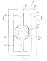
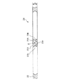
図1は、本発明の第1実施形態に係る光スキャナー(アクチュエーター)を示す平面図、図2は、図1中のA−A線断面図、図3は、図1に示す光スキャナーに備えられた可動板を説明するための平面図、図4は、図1中のB−B線断面図、図5は、図4の部分拡大断面図である。図6は、図1に示す光スキャナーの製造方法を説明する断面図、図7は、図1に示す光スキャナーの製造方法を説明する断面図である。図8は、図1に示す光スキャナーの製造方法を説明する断面図、図9は、図8(e)に示すエッチング工程における連結部の形成(マスクずれのない場合)を説明するための図、図10は、図8(e)に示すエッチング工程における連結部の形成(マスクずれのある場合)を説明するための図である。なお、以下では、説明の便宜上、図2、4〜10中の上側を「上」、下側を「下」と言う。
Hereinafter, preferred embodiments of an actuator, an optical scanner, and an image forming apparatus of the present invention will be described with reference to the accompanying drawings. In this embodiment, a case where the actuator of the present invention is applied to an optical scanner will be described as an example.
<First Embodiment>
First, a first embodiment of the optical scanner of the present invention will be described.
1 is a plan view showing an optical scanner (actuator) according to the first embodiment of the present invention, FIG. 2 is a cross-sectional view taken along line AA in FIG. 1, and FIG. 3 is provided in the optical scanner shown in FIG. FIG. 4 is a sectional view taken along the line BB in FIG. 1, and FIG. 5 is a partially enlarged sectional view of FIG. 6 is a cross-sectional view illustrating a method for manufacturing the optical scanner shown in FIG. 1, and FIG. 7 is a cross-sectional view illustrating a method for manufacturing the optical scanner shown in FIG. FIG. 8 is a cross-sectional view for explaining the manufacturing method of the optical scanner shown in FIG. 1, and FIG. 9 is a view for explaining the formation of a connecting portion (when there is no mask displacement) in the etching step shown in FIG. FIG. 10 is a view for explaining the formation of a connecting portion (when there is a mask shift) in the etching step shown in FIG. In the following, for convenience of explanation, the upper side in FIGS. 2, 4 to 10 is referred to as “upper”, and the lower side is referred to as “lower”.
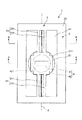
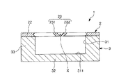
図1に示すように、光スキャナー1は、振動系を有する基体2と、基体2を支持する支持体3と、基体2の振動系を振動させる駆動部4とを有する。
また、基体2は、光反射部211が設けられた可動板(可動部)21と、可動板21に連結する1対の連結部23、24と、1対の連結部23、24とを支持する支持部22とを有している。支持部22は連結部23、24を介して可動板21を支持しているとも言え、1対の連結部23、24は可動板21と支持部22とを連結しているとも言える。
このような光スキャナー1では、駆動部4の駆動力により、各連結部23、24を捩り変形させながら、可動板21を連結部23、24に沿った所定の軸まわりに回動させる。これにより、光反射部211で反射した光を所定の一方向に走査することができる。
As shown in FIG. 1, the
The
In such an
以下、光スキャナー1を構成する各部を順次詳細に説明する。
[基体]
基体2は、前述したように、光反射部211が設けられた可動板21と、可動板21を支持する支持部22と、可動板21と支持部22とを連結する1対の連結部23、24とを有する。
Hereinafter, each part which comprises the
[Substrate]
As described above, the
このような基体2は、シリコンを主材料として構成されており、可動板21、支持部22および連結部23、24が一体的に形成されている。より具体的には、基体2は、後に詳述するように、板面がシリコンの(100)面で構成されたシリコン基板を異方性エッチングすることにより形成されたものである。このような異方性エッチングにより、シリコンの(111)面をエッチング停止層として利用して簡単かつ高精度に、可動板21、支持部22および1対の連結部23、24を形成することができる。なお、シリコン基板としては、一般的に単結晶シリコン基板が用いられる。
また、このような基体2の上面および下面は、それぞれ、シリコンの(100)面で構成されている。また、支持部22の内周面、可動板21の側面、および、各連結部23、24の側面の軸線Xに平行な部分は、それぞれ、シリコンの(111)面で構成されている。
Such a base |
Moreover, the upper surface and lower surface of such a base |
また、シリコンは軽量かつSUSなみの剛性を有するため、基体2がシリコンを主材料として構成されていることにより、優れた振動特性を有する基体2が得られる。また、シリコンは後述するようにエッチングにより高精度な寸法精度で加工が可能であるので、シリコン基板を用いて基体2を形成することにより、所望の形状(所望の振動特性)を有する基体2を得ることができる。
In addition, since silicon is light and has a rigidity similar to SUS, the
以下、基体2についてさらに詳述する。
支持部22は、図1に示すように、枠状をなしている。より具体的には、支持部22は、四角環状をなしている。このような支持部22は、1対の連結部23、24を介して可動板21を支持する。なお、支持部22の形状としては、1対の連結部23、24を介して可動板21を支持することができれば、特に限定されず、例えば、各連結部23、24に対応して分割された形状をなしていてもよい。
Hereinafter, the
As shown in FIG. 1, the
このような支持部22の内側には、可動板21が設けられている。
可動板21は、板状をなしている。また、本実施形態では、可動板21は、可動板21の板厚方向からの平面視にて、可動板21の回動中心軸(軸線X)に沿った1対の辺と軸線Xに対して垂直な方向(線分Yに沿った方向)に沿った1対の辺とで構成された四角形の四隅の部分をそれぞれ四角形に欠いた形状(十字状)をなしている。これにより、可動板21の上面の光反射部211の面積(光反射領域)を十分に確保しつつ、可動板21の回動時の慣性モーメントを低減することができる。また、このような可動板21は後に詳述するようにシリコン基板を異方性エッチングすることにより、簡単かつ高精度に形成することができる。
A
The
より具体的に説明すると、図3に示すように、可動板21は、本体部212と、この本体部212から軸線Xに平行な方向に両側へ突出する1対の突出部(第2突出部)213、214と、本体部212から軸線Xに垂直な方向(線分Yに平行な方向)に両側に突出する1対の突出部(第1突出部)215、216とで構成されている。このような1対の突出部213、214および1対の突出部215、216を有する可動板21は、板厚方向からの平面視にて十字状をなす。
More specifically, as shown in FIG. 3, the
そして、可動板21の外周に沿った方向における突出部213と突出部215との間には、欠損部251が形成されている。また、可動板21の外周に沿った方向における突出部213と突出部216との間には、欠損部252が形成されている。また、可動板21の外周に沿った方向における突出部214と突出部216との間には、欠損部254が形成されている。また、可動板21の外周に沿った方向における突出部214と突出部215との間には、欠損部253が形成されている。
言い換えると、可動板21の板厚方向からの平面視において、可動板21(本体部212)の外周に沿って、欠損部251、突出部213、欠損部252、突出部216、欠損部254、突出部214、欠損部252、突出部215がこの順で並んで設けられている。
A missing
In other words, in a plan view from the thickness direction of the
また、欠損部251と欠損部252とは突出部213を介して対向している。また、欠損部252と欠損部254とは突出部216を介して対向している。また、欠損部253と欠損部254とは突出部214を介して対向している。また、欠損部251と欠損部253とは突出部215を介して対向している。
このような突出部213〜216および欠損部251〜254は、それぞれ、可動板21の板厚方向からの平面視にて四角形をなしている。なお、図1、3では、各欠損部251〜254の平面視形状が正方形をなす状態を一例として図示している。また、突出部213〜216および欠損部251〜254の平面視形状の角部が丸み付けされていてもよい。可動板21の十字状の外形における角部には、所定の結晶面だけではなく複数の結晶面が現れるため角部は厳密には直角とならず、各欠損部251〜254は厳密には四角形ではない。しかし、本実施形態においては、上記の状態を含めて各欠損部251〜254は四角形であるとみなす。
Further, the
Such projecting
このような可動板21の板厚方向からの平面視における外形は、主として、可動板21の回動中心軸(軸線X)に平行な線分と、可動板21の回動中心軸(軸線X)に対して垂直な線分(線分Y)とで構成されている。これにより、後述するようにシリコン基板を異方性エッチングすることにより、可動板21を簡単かつ高精度に形成することができる。なお、可動板21の十字状の外形における角部には、所定の結晶面だけではなく複数の結晶面が現れる。従って、可動板21の板厚方向からの平面視における角部の外形は軸線Xまたは線分Yに必ずしも平行な線分とならない。すなわち、可動板21の板厚方向からの平面視における外形は、少なくとも上記の可動板21の角部を除いて、軸線Xに平行な線分と線分Yに平行な線分とで構成されている。
The outer shape of the
また、可動板21は、平面視にて可動板21の回動中心軸(軸線X)に対して対称な形状をなしている。これにより、簡単に、可動板21の重心を可動板21の回動中心軸上に位置させ、可動板21の回動を円滑なものとすることができる。
また、可動板21は、平面視にて可動板21の中心Pを通りかつ可動板21の回動中心軸(軸線X)に対して垂直な線分Yに対して対称な形状をなしている。これにより、可動板の設計が容易となる。
Further, the
Further, the
また、可動板21の板面(上面および下面)は、シリコンの(100)面で構成されている。これにより、後述するように板面が(100)面で構成されたシリコン基板を異方性エッチングすることにより、可動板21、支持部22および1対の連結部23、24を簡単かつ高精度に形成することができる。
また、可動板21の側面(特に軸線Xに平行な面)は、主として、シリコンの(111)面で構成されている。これにより、後述するように板面が(100)面で構成されたシリコン基板を異方性エッチングすることにより、シリコンの(111)面をエッチングの停止層として利用し、可動板21、支持部22および1対の連結部23、24を簡単かつ高精度に形成することができる。なお、可動板21の板厚方向からの平面視における外形の角部においては、可動板21の側面は(111)面以外の結晶面を含んでいる。従って、可動板21の側面は、少なくとも当該角部における側面を除いて、シリコンの(111)面で構成されている。
Further, the plate surface (upper surface and lower surface) of the
Further, the side surface (particularly, the surface parallel to the axis X) of the
また、可動板21の側面には、可動板21の板面に直交する横断面においてV字状をなす溝217が形成されている。これにより、可動板21の慣性モーメントを低減することができる。また、このような溝は、板面が(100)面で構成されたシリコン基板を異方性エッチングすることにより、シリコンの(111)面をエッチングの停止層として利用し、簡単かつ高精度に形成することができる。
Further, a
また、可動板21の板厚方向からの平面視における回動中心軸(軸線X)に対して垂直な方向(以下、「線分Y方向」とも言う)での長さをAとし、可動板21の回動中心軸(軸線X)に平行な方向(以下、「軸線X方向」とも言う)での長さをBとし、各欠損部251〜254の線分Y方向に沿った長さをaとし、各欠損部251〜254の軸線X方向に沿った長さをbとしたとき、下記式(A)、(B)をそれぞれ満たす。なお、ここで、上記aは、可動板21の平面視における各突出部(第1突出部)215、216の突出長さに等しく、また、上記bは、可動板21の平面視における各突出部(第2突出部)213、214の突出長さに等しい。
The length of the
上記式(A)、(B)をそれぞれ満たすことにより、可動板21の光反射部211の光反射に必要な面積を確保しつつ、可動板21の回動時における慣性モーメントを効率的に低減することができる。
これに対し、長さa、bがそれぞれ前記下限値未満であると、可動板21の回動時における慣性モーメントを低減する効果が小さい傾向となる。そのため、可動板21の厚さによっては、可動板21の動撓みが大きくなり、光スキャナー1の光学特性を低下させる場合がある。
By satisfying each of the above formulas (A) and (B), the moment of inertia when the
On the other hand, when the lengths a and b are each less than the lower limit value, the effect of reducing the moment of inertia when the
一方、長さa、bが前記上限値を超えると、可動板21の光反射部211の面積を効率的に用いることができず、光反射部211での反射光の強度が小さくなる傾向を示す。
なお、図3では、上記式(A)、(B)を満たし、a、bをそれぞれ最大とした場合の可動板21A、a、bをそれぞれ最小とした場合の可動板21Bをそれぞれ鎖線で示している。
On the other hand, if the lengths a and b exceed the upper limit, the area of the
In FIG. 3, the
以下、上記式(A)、(B)について簡単に説明する。
図3に示すように平面視にて可動板21に光Lの円形または楕円形のスポットが内接する場合、各欠損部251〜254が光Lのスポットの外側で面積が最大となるのは、a=(1−1/√2)A、b=(1−1/√2)Bである。また、このとき、各欠損部251〜254の角P3が光Lのスポットの外周縁状に位置し、a/b=A/Bである。
The above formulas (A) and (B) will be briefly described below.
As shown in FIG. 3, when the circular or elliptical spot of the light L is inscribed in the
また、かかる場合、欠損部251〜254を形成することによる効果(特に可動板21の慣性モーメントを低減する効果)が発揮される範囲において、aが最大となりbが最小となるのは、軸線Xに対して30°傾斜した線分と光Lのスポットの外周縁との交点P2に各欠損部251〜254の角P3が位置するときである。このとき、a、bは、下記式のようになる。
Further, in such a case, in the range where the effect (particularly the effect of reducing the moment of inertia of the movable plate 21) due to the formation of the missing
また、かかる場合、欠損部251〜254を形成することによる効果(特に可動板21の慣性モーメントを低減する効果)が発揮される範囲において、aが最小となりbが最大となるのは、軸線Xに対して60°傾斜した線分と光Lのスポットの外周縁との交点P1に各欠損部251〜254の角P3が位置するときである。このとき、a、bは、下記式のようになる。
Further, in such a case, in the range where the effect (particularly the effect of reducing the moment of inertia of the movable plate 21) due to the formation of the missing
さらに、光Lとして通常用いられるレーザーのスポット径の有効範囲は、一般的にピーク輝度の1/e2以上となる輝度の範囲とされる。したがって、その有効範囲が光反射部211内に収まっていれば、理想的な光反射を行うことができる。
ただし、実際のレーザーは、上記有効範囲の外側であっても、若干の光が存在する。また、可動板21の回動時の慣性モーメントは、可動板21の動撓みが波長λ/4以下となるように抑えられていればよい。よって、a、bが上記値に対して若干小さかったり大きかったりしても、実使用上問題なく許容できる。
Furthermore, the effective range of the spot diameter of a laser that is normally used as the light L is generally a luminance range that is 1 / e 2 or more of the peak luminance. Therefore, if the effective range is within the
However, an actual laser has some light even outside the effective range. In addition, the moment of inertia when the
具体的には、上述したように求めたa、bの許容範囲を−20%以上+200%以下とすることができる。
ここで、A=B=2.0mm、a=(1−1/√2)A[mm]、b=(1−1/√2)B[mm]とした場合を基準として、a、bをそれぞれ−20%とした場合、−200%とした場合、+205%とした場合の可動板21での反射光の輝度を目視により評価した結果を表1に示す。
Specifically, the allowable range of a and b obtained as described above can be set to −20% or more and + 200% or less.
Here, with reference to the case where A = B = 2.0 mm, a = (1-1 / √2) A [mm], and b = (1-1 / √2) B [mm], a, b Table 1 shows the results of visual evaluation of the brightness of the reflected light from the
表1において、「◎」は、反射光の輝度が十分であることを示し、「○」は、反射光の輝度が実使用上問題ないことを示し、「△」、反射光の輝度が不十分であることを示している。
また、上述したように、動撓みの許容範囲は、波長λ/4以下とされている。したがって、例えばλ=530nmの場合、動撓みの許容範囲は、133nm以下である。上記基準において、FEM解析により、機械角10°、駆動周波数18kHzで駆動したときの動撓みを求めると、動撓み量が122nmであり、上記許容範囲内となる。また、上記基準の−20%において、FEM解析により、機械角10°、駆動周波数18kHzで駆動したときの動撓みを求めると、動撓み量が130nmであり、上記許容範囲内となる。これに対し、上記基準の−25%において、FEM解析により、機械角10°、駆動周波数18kHzで駆動したときの動撓みを求めると、動撓み量が140nmであり、上記許容範囲外となる。
以上のようなことから、上記式(A)、(B)が得られる。
In Table 1, “◎” indicates that the brightness of the reflected light is sufficient, “◯” indicates that the brightness of the reflected light is not a problem in practical use, and “Δ” indicates that the brightness of the reflected light is not satisfactory. It is enough.
Further, as described above, the allowable range of dynamic deflection is set to a wavelength λ / 4 or less. Therefore, for example, in the case of λ = 530 nm, the allowable range of dynamic deflection is 133 nm or less. In the above criteria, when the dynamic deflection when driving at a mechanical angle of 10 ° and a drive frequency of 18 kHz is obtained by FEM analysis, the amount of dynamic deflection is 122 nm, which falls within the allowable range. Further, when -20% of the above standard is obtained by FEM analysis to determine the dynamic deflection when driven at a mechanical angle of 10 ° and a drive frequency of 18 kHz, the dynamic deflection amount is 130 nm, which is within the allowable range. On the other hand, when the dynamic deflection at the mechanical angle of 10 ° and the driving frequency of 18 kHz is obtained by FEM analysis at −25% of the standard, the dynamic deflection amount is 140 nm, which is outside the allowable range.
From the above, the above formulas (A) and (B) are obtained.
また、可動板21は、上記長さAおよびBは、互いに等しくても異なっていてもよい。なお、図1では、A=Bの場合を図示している。
本実施形態では、可動板21の平面視における四隅の部分(欠損部251〜254)のそれぞれについて、a≦bの関係を満たす。これにより、可動板21の回動時の慣性モーメントを最も効果的に低減することができる。
また、下記式(C)および(D)を満たすのがより好ましい。
Further, the lengths A and B of the
In the present embodiment, the relationship of a ≦ b is satisfied for each of the four corner portions (
Moreover, it is more preferable to satisfy | fill following formula (C) and (D).
これにより、可動板21の光反射領域をより最適に確保しながら、可動板21の回動時の慣性モーメントを効果的に低減することができる。
このような可動板21の上面には、光反射性を有する光反射部211が設けられている。一方、可動板21の下面には、後述する駆動部4の永久磁石41が設けられている。なお、永久磁石41については、後述する駆動部4の説明において詳述する。
Thereby, the moment of inertia at the time of rotation of the
On the upper surface of the
各連結部23、24は、長手形状をなしており、弾性変形可能に構成されている。また、連結部23および連結部24は可動板21を介して対向している。このような連結部23、24は、それぞれ、可動板21を支持部22に対して回動可能とするように、可動板21と支持部22とを連結している。1対の連結部23、24は、軸線Xに沿って同軸的に設けられており、この軸線Xを回動中心軸として、可動板21が支持部22に対して回動する。
Each connecting
本実施形態では、図1に示すように、連結部23は、1対の梁部材231、232で構成されている。同様に、連結部24は、1対の梁部材241、242で構成されている。 このように構成された連結部23、24は、連結部が1本で構成された場合よりも長さを短くすることが可能となり、光スキャナー1の板厚方向の平面視における面積を小さくすることができる。以下、連結部23について代表的に説明し、連結部24については、連結部23と同様であるので、その説明を省略する。
In the present embodiment, as shown in FIG. 1, the connecting
各梁部材231、232は、軸線Xに沿って設けられているとともに、軸線Xを介して対向している。また、各梁部材231、232は、その横断面形状が平行四辺形をなしている。
より具体的には、各梁部材231、232の横断面の外形は、それぞれ、シリコンの(100)に沿った1対の辺と、シリコンの(111)面に沿った1対の辺とで構成された平行四辺形をなしている。すなわち、梁部材231は、上面2311および下面2312がそれぞれシリコンの(100)面で構成され、1対の側面2313、2314がそれぞれシリコンの(111)面で構成されている。同様に、梁部材232は、上面2321および下面2322がそれぞれシリコンの(100)面で構成され、1対の側面2323、2324がそれぞれシリコンの(111)面で構成されている。ここで、側面2313、2314、2323、2324は、それぞれ、シリコンの(111)面で構成されているので、基体2の上面または下面(すなわちシリコンの(100)面)に対する傾斜角θが54.73°となっている。このような横断面形状をなす各梁部材231、232は、板面がシリコンの(100)面で構成されたシリコン基板を異方性エッチングすることにより簡単かつ確実に形成することができる。
このように連結部23の外表面がシリコンの(100)面および(111)面で構成されていると、後述するようにシリコンの(111)面をエッチングの停止層として利用し、簡単かつ高精度に連結部23を形成することができる。
Each
More specifically, the cross-sectional outlines of the
As described above, when the outer surface of the connecting
また、梁部材231、232は、軸線Xに平行な方向からみたときに(言い換えると、図5に示す断面でみたとき)、上下に延び軸線Xを通る線分に対して対称な形状をなしている。
また、図5に示す断面において、連結部23全体の幅(梁部材231の側面2313と梁部材232の側面2323との面間距離)は、下側から上側に向けて拡がっている。
In addition, the
Further, in the cross section shown in FIG. 5, the entire width of the connecting portion 23 (the inter-surface distance between the
また、図5に示す断面において、梁部材231と梁部材232との間の距離(隙間の幅)は、下側から上側に向けて拡がっている。
すなわち、1対の梁部材231、232間の距離は、可動板21の回動中心軸に平行な方向からみたときに、可動板21の一方の面側から他方の面側に向けて(本実施形態では下側から上側に向けて)漸増している。
In the cross section shown in FIG. 5, the distance (gap width) between the
That is, the distance between the pair of
このような連結部23は、後述するようにシリコン基板を異方性エッチングすることにより、前述したような平面視形状をなす可動板21と一括して簡単かつ高精度に形成することができる。
また、1対の梁部材231、232の下側の端同士の間の距離をW1とし、1対の梁部材231、232の可動板21の厚さ方向での厚さをtとしたとき、下記式(1)を満たす。
Such a connecting
When the distance between the lower ends of the pair of
後述に詳述するように、板面がシリコンの(100)面で構成されたシリコン基板をその両面側から異方性エッチングするため、可動板21、支持部22および1対の連結部23、24を形成する際に、シリコン基板の両面に形成したマスクの形成位置がずれることがある。このように、シリコン基板の両面のマスクの形成位置がずれると、各梁部材231、232のシリコンの(111)面で構成されるべき1対の側面2313、2314、2323、2324に段差が生じてしまう。上記式(1)を満たすことにより、シリコン基板の両面に形成したマスクの形成位置がずれた場合に、一方の側面に形成された段差と、他方の側面に形成された段差とをシリコン基板の厚さ方向にずらすことができる(図10参照)。そのため、可動板21の回動時における各梁部材231、232に生じる応力集中を緩和することができる。
このようにして、光スキャナー1は、駆動時の応力集中による破損を比較的簡単に防止することができる。
また、1対の梁部材231、232の上側の端同士の間の距離をW2としたとき、下記式(2)を満たす。
As will be described in detail later, in order to anisotropically etch a silicon substrate having a (100) plane of silicon from both sides, a
In this way, the
Further, when the distance between the upper end between the pair of
これにより、板面がシリコンの(100)面で構成されたシリコン基板をその両面側から異方性エッチングすることにより、1対の梁部材231、232で構成された連結部23を簡単かつ確実に形成することができる。
As a result, the silicon substrate whose plate surface is composed of the (100) surface of silicon is anisotropically etched from both sides thereof, so that the connecting
[支持体]
支持体3は、前述した基体2を支持する機能を有する。また、支持体3は、後述する駆動部4のコイル42を支持する機能をも有する。
この支持体3は、上方に開放する凹部31を有する箱状をなしている。言い換えると、支持体3は、板状をなす板状部32と、その板状部32の上面の外周部に沿って設けられた枠状をなす枠状部33とで構成されている。
このような支持体3の上面のうち凹部31の外側の部分、すなわち、枠状部33の上面には、前述した基体2の支持部22の下面が接合されている。これにより、基体2の可動板21および1対の連結部23、24と支持体3との間には、可動板21の回動を許容する空間が形成されている。
[Support]
The support 3 has a function of supporting the
The support 3 has a box shape having a
The lower surface of the
このような支持体3の構成材料としては、特に限定されないが、例えば、石英ガラス、パイレックスガラス(「パイレックス」は登録商標)、テンパックスガラス等のガラス材料や、単結晶シリコン、ポリシリコン等のシリコン材料、LTCC(低温焼結セラミックス)等が挙げられる。
また、基体2と支持体3との接合方法としては、支持体3の構成材料、形状等に応じて適宜決められるものであり、特に限定されないが、接着剤を用いた方法、陽極接合法、直接接合法等が挙げられる。
The constituent material of the support 3 is not particularly limited, and examples thereof include glass materials such as quartz glass, Pyrex glass (“Pyrex” is a registered trademark), Tempax glass, single crystal silicon, polysilicon, and the like. Examples thereof include silicon materials and LTCC (low temperature sintered ceramics).
Further, the bonding method between the
[駆動部]
駆動部4は、永久磁石41およびコイル42を有し、前述した基体2の可動板21を電磁駆動方式(より具体的にはムービングマグネット型の電磁駆動方式)により回動駆動させるものである。電磁駆動方式は、大きな駆動力を発生させることができる。そのため、電磁駆動方式を採用する駆動部4によれば、低駆動電圧化を図りつつ、可動板21の振れ角を大きくすることができる。
[Drive part]
The drive unit 4 includes a
永久磁石41は、可動板21の下面に例えば接着剤を介して固定されている。また、永久磁石41は、長手形状をなしており、平面視にて軸線Xに対して直交する方向に延在するように設けられている。このような永久磁石41は、長手方向に磁化しており、長手方向の一方側がS極、他方側がN極となっている。永久磁石41を軸線Xに対して直交する方向に延在するように設けることにより、永久磁石41の両端部を軸線Xから離れたところに位置させることができる。そのため、コイル42が発生する磁界の作用により、可動板21により大きなトルクを与えることができる。
このような永久磁石41としては、特に限定されず、例えば、ネオジウム磁石、フェライト磁石、サマリウムコバルト磁石、アルニコ磁石、ボンド磁石などの、硬磁性体を着磁したものを好適に用いることができる。
The
Such a
コイル42は、支持体3の凹部31の底面311上に、可動板21と対向するように設けられている。これにより、コイル42が発生する磁界を永久磁石41に効果的に作用させることができる。このコイル42は、図示しない電源に電気的に接続されており、電源から周期的に変化する電圧(交番電圧、間欠的な直流等)が印加されるようになっている。
The
このような駆動部4によって、次のように可動板21が回動する。
まず、図示しない電源によりコイル42に例えば交番電圧を印加する。これにより、コイル42の上側(可動板21側)がN極、下側がS極となる第1の磁界と、コイル42の上側がS極、下側がN極となる第2の磁界とが、交互にかつ周期的に発生する。
第1の電界では、永久磁石41のN極側がコイル42に引きつけられ、反対にS極側がコイル42から遠ざかるように、可動板21が軸線Xを中心に図2にて反時計回りに回動する(第1の状態)。反対に、第2の電界では、永久磁石41のS極側がコイル42に引きつけられ、反対にN極側がコイル42から遠ざかるように、可動板21が軸線Xを中心に図2にて時計回りに回動する(第2の状態)。このような第1の状態と第2の状態とが交互に繰り返され、可動板21が軸線Xを中心に回動する。
The
First, for example, an alternating voltage is applied to the
In the first electric field, the
(アクチュエーターの製造方法)
以上のような光スキャナー1は、例えば、次のようにして製造することができる。以下、本発明のアクチュエーターの製造方法の一例として、図6ないし図10に基づいて、光スキャナー1の製造方法を説明する。また、図6ないし図8は、それぞれ、図2に対応する断面で示されており、図9および図10は、それぞれ、図5に対応する断面で示されている。
光スキャナー1の製造方法は、基体2を形成する工程を有する。
基体2を形成する工程は、[A]凹部218を形成する工程と、[B]可動板21、支持部22および1対の連結部23、24を形成する工程とを有する。
(Actuator manufacturing method)
The
The method for manufacturing the
The step of forming the
以下、各工程を順次詳細に説明する。
[A]凹部218を形成する工程
−A1−
まず、図6(a)に示すように、シリコン基板102を用意する。
このシリコン基板102は、後述するエッチングを経ることにより基体2となるものである。
具体的には、シリコン基板102は、その主面がシリコンの(100)面で構成されたものである。
Hereinafter, each process will be described in detail.
[A] Step of forming recess 218 -A1-
First, as shown in FIG. 6A, a
The
Specifically, the
−A2−
次に、図6(b)に示すように、シリコン基板102の上面上に窒化膜51を形成するとともに、シリコン基板102の下面上に窒化膜52を形成する。
この窒化膜51、52は、それぞれ、例えば、SiNで構成されている。
また、窒化膜51、52の形成方法は、ぞれぞれ、特に限定されないが、例えば、プラズマCVD等の気相成膜法を用いることができる。
また、窒化膜51、52の厚さは、特に限定されないが、0.01μm以上0.2μm以下程度である。
なお、窒化膜51、52に代えて、SiOで構成された酸化膜を例えば熱酸化法により形成してもよい。
-A2-
Next, as shown in FIG. 6B, a
The
The method for forming the
The thicknesses of the
Instead of the
−A3−
次に、図6(c)に示すように、窒化膜51上にレジスト膜61を形成し、図6(d)に示すように、窒化膜52上にレジスト膜62を形成する。
このレジスト膜61、62は、それぞれ、ポジ型またはネガ型のレジスト材料で構成されている。
−A4−
次に、レジスト膜62を露光および現像することにより、レジスト膜62の凹部218の形成領域に対応した部分を除去する。これにより、図6(e)に示すように、開口621を有するレジスト膜62Aを得る。
-A3-
Next, a resist
The resist
-A4-
Next, the resist
−A5−
次に、レジスト膜62Aをマスクとして用いて、窒化膜52の一部をエッチングにより除去する。これにより、図6(f)に示すように、開口521を有する窒化膜52Aを得る。
上記エッチング(開口521の形成方法)としては、特に限定されないが、例えば、リアクティブイオンエッチング(RIE)、CF4を用いたドライエッチング等が挙げられる。
-A5-
Next, part of the
The etching (a method for forming the opening 521) is not particularly limited, and examples thereof include reactive ion etching (RIE), dry etching using CF 4, and the like.
−A6−
次に、レジスト膜61、62Aを除去する。これにより、図6(g)に示すように、シリコン基板102は、その上面が窒化膜51で覆われ、下面が窒化膜52Aで覆われた状態となる。
レジスト膜61、62の除去方法としては、特に限定されないが、例えば、硫酸による洗浄、O2アッシング等が挙げられる。
-A6-
Next, the resist
The method for removing the resist
−A7−
次に、窒化膜52Aをマスクとして用いて、シリコン基板102をエッチングする。これにより、図7(a)に示すように、凹部218を有するシリコン基板102Aを得る。
上記エッチング(凹部218の形成方法)としては、特に限定されないが、後述する可動板21、支持部22等の形成のためのエッチングと同様、異方性エッチングが好適に用いられる。
かかる異方性エッチングは、特に限定されないが、例えば、KOH水溶液等を用いたウェットエッチングにより行うことができる。
-A7-
Next, the
The etching (a method for forming the recess 218) is not particularly limited, but anisotropic etching is preferably used as in the etching for forming the
Such anisotropic etching is not particularly limited, but can be performed by, for example, wet etching using a KOH aqueous solution or the like.
−A8−
次に、窒化膜51、52Aを除去する。これにより、図7(b)に示すように、シリコン基板102Aの上面および下面が露出した状態となる。
窒化膜51、52Aの除去方法としては、特に限定されないが、上記工程A5と同様、例えば、リアクティブイオンエッチング(RIE)、CF4を用いたドライエッチング等が挙げられる。
-A8-
Next, the
The method for removing the
[B]可動板21、支持部22等を形成する工程
−B1−
次に、図7(c)に示すように、シリコン基板102Aの上面上に窒化膜71を形成するとともに、シリコン基板102Aの下面上に窒化膜72を形成する。
この窒化膜71、72は、それぞれ、例えば、SiNで構成されている。
[B] Step of forming
Next, as shown in FIG. 7C, a
The
また、窒化膜71、72の形成方法は、ぞれぞれ、特に限定されないが、上記工程A2と同様、例えば、プラズマCVD等の気相成膜法を用いることができる。
また、窒化膜71、72の厚さは、特に限定されないが、0.01μm以上0.3μm以下程度である。
なお、窒化膜71、72に代えて、SiOで構成された酸化膜を例えば熱酸化法により形成してもよい。
In addition, although the method for forming the
The thicknesses of the
Instead of the
−B2−
次に、図7(d)に示すように、窒化膜71上にレジスト膜81を形成する。
このレジスト膜81は、ポジ型またはネガ型のレジスト材料で構成されている。
−B3−
次に、レジスト膜81を露光および現像することにより、レジスト膜81の可動板21、支持部22および1対の連結部23、24の形成領域に対応した部分が残存するように、レジスト膜81の一部を除去する。これにより、図7(e)に示すように、開口811を有するレジスト膜81Aを得る。なお、図7(e)では図示しないが、レジスト膜81Aには、1対の梁部材231、232の上端同士の間の隙間に対応して形成された開口も形成されている。
-B2-
Next, as shown in FIG. 7D, a resist film 81 is formed on the
The resist film 81 is made of a positive or negative resist material.
-B3-
Next, the resist film 81 is exposed and developed, so that portions corresponding to the formation regions of the
−B4−
次に、レジスト膜81Aをマスクとして用いて、窒化膜71の一部をエッチングにより除去する。これにより、図7(f)に示すように、開口711を有する窒化膜71Aを得る。なお、図7(f)では図示しないが、窒化膜71Aには、1対の梁部材231、232の上端同士の間の隙間に対応して形成された開口も形成されている。
上記エッチング(開口711の形成方法)としては、特に限定されないが、上記工程A5と同様、例えば、リアクティブイオンエッチング(RIE)、CF4を用いたドライエッチング等が挙げられる。
-B4-
Next, a part of the
The etching (a method for forming the opening 711) is not particularly limited, and examples thereof include reactive ion etching (RIE), dry etching using CF 4 , and the like, as in the step A5.
−B5−
次に、レジスト膜81Aを除去する。これにより、図7(g)に示すように、シリコン基板102Aは、その上面が窒化膜71Aで覆われ、下面が窒化膜72で覆われた状態となる。
レジスト膜81Aの除去方法としては、特に限定されないが、例えば、硫酸による洗浄、O2アッシング等が挙げられる。
-B5-
Next, the resist
The method for removing the resist
−B6−
次に、図8(a)に示すように、窒化膜72上にレジスト膜82を形成する。
このレジスト膜82は、ポジ型またはネガ型のレジスト材料で構成されている。
−B7−
次に、レジスト膜82を露光および現像することにより、レジスト膜82の可動板21、支持部22および1対の連結部23、24の形成領域に対応した部分が残存するように、レジスト膜82の一部を除去する。これにより、図8(b)に示すように、開口821を有するレジスト膜82Aを得る。なお、図8(b)では図示しないが、レジスト膜82Aには、1対の梁部材231、232の下端同士の間の隙間に対応して形成された開口も形成されている。
-B6-
Next, as illustrated in FIG. 8A, a resist
The resist
-B7-
Next, the resist
−B8−
次に、レジスト膜82Aをマスクとして用いて、窒化膜72の一部をエッチングにより除去する。これにより、図8(c)に示すように、開口721を有する窒化膜72Aを得る。なお、図8(c)では図示しないが、窒化膜72Aには、1対の梁部材231、232の下端同士の間の隙間に対応して形成された開口も形成されている。
上記エッチング(開口721の形成方法)としては、特に限定されないが、上記工程A5と同様、例えば、リアクティブイオンエッチング(RIE)、CF4を用いたドライエッチング等が挙げられる。
-B8-
Next, a part of the
The etching (a method for forming the opening 721) is not particularly limited, and examples thereof include reactive ion etching (RIE), dry etching using CF 4 , and the like as in step A5.
−B9−
次に、レジスト膜82Aを除去する。これにより、図8(d)に示すように、シリコン基板102Aは、その上面が窒化膜71Aで覆われ、下面が窒化膜72Aで覆われた状態となる。
レジスト膜82Aの除去方法としては、特に限定されないが、例えば、硫酸による洗浄、O2アッシング等が挙げられる。
-B9-
Next, the resist
A method for removing the resist
−B10−
次に、窒化膜71A、72Aをマスクとして用いて、シリコン基板102Aを異方性エッチングする。これにより、図8(e)に示すように、基体2を得る。すなわち、本工程の異方性エッチングでは、第1のマスクである窒化膜72Aと第2のマスクである窒化膜71Aとを介してシリコン基板102Aをその両面側から異方性エッチングすることにより、可動板21、支持部22および1対の連結部23、24を形成する。
上記異方性エッチング(基体2の形成方法)は、特に限定されないが、例えば、KOH水溶液等を用いたウェットエッチングにより行うことができる。
ここで、かかる異方性エッチングによる連結部23の形成について詳述する。なお、連結部24の形成については、連結部23の形成と同様であるので、その説明を省略する。
-B10-
Next, the
The anisotropic etching (method for forming the substrate 2) is not particularly limited, but can be performed by, for example, wet etching using a KOH aqueous solution or the like.
Here, formation of the
図9に示すように、マスク(第2のマスク)として用いる窒化膜71Aは、連結部23の梁部材231の上面の形成領域に対応して形成された部分712と、連結部23の梁部材232の上面の形成領域に対応して形成された部分713とを有し、部分712と部分713との間には、開口(第2の開口)714が形成されている。この開口714は、1対の梁部材231、232の上端同士の間の隙間に対応して形成されている。
As shown in FIG. 9, the
また、マスク(第1のマスク)として用いる窒化膜72Aは、連結部23の梁部材231の下面の形成領域に対応して形成された部分722と、連結部23の梁部材232の下面の形成領域に対応して形成された部分723とを有し、部分722と部分723との間には、開口724(第1の開口)が形成されている。この開口724は、1対の梁部材231、232の下端同士の間の隙間に対応して形成されている。
ここで、開口724の幅をWm1とし、シリコン基板102Aの厚さをTとしたときに、下記式(3)の関係を満たす。
The
Here, when the width of the
このような関係式を満たすことにより、第1のマスクである窒化膜72Aと第2のマスクである窒化膜71Aとの位置関係がずれ、それにより、各梁部材231、232のシリコンの(111)面で構成されるべき1対の側面に段差が生じても、一方の側面に形成された段差と、他方の側面に形成された段差とをシリコン基板の厚さ方向にずらすことができる。そのため、得られたアクチュエーターにおいて、可動板21の回動時における各梁部材231、232に生じる応力集中を緩和することができる。
開口714の幅をWm2としたとき、下記式(4)を満たす。
By satisfying such a relational expression, the positional relationship between the
When the width of the
これにより、板面がシリコンの(100)面で構成されたシリコン基板102Aをその両面側から異方性エッチングすることにより、1対の梁部材231、232で構成された連結部23を簡単かつ確実に形成することができる。
以下、本工程の異方性エッチングにおける段差の発生について詳述する。
本工程における異方性エッチングに際し、マスクとして用いる窒化膜71A、72Aの形成位置がずれていない場合、図9(a)〜図9(d)に示すように、開口711、714を介してシリコン基板102Aの上面がエッチングされるとともに、開口721、724を介してシリコン基板102Aの下面がエッチングされていき、1対の梁部材231、232が形成される。
この場合、開口714および開口724の幅方向での中心位置が互いに幅方向で一致しているので、図9(d)に示すように、各梁部材231、232の各側面は、段差のない、シリコンの(111)面で構成された一定の傾斜面となる。
As a result, the
Hereinafter, the generation of a step in the anisotropic etching in this step will be described in detail.
In the anisotropic etching in this step, when the formation positions of the
In this case, since the center positions in the width direction of the
一方、本工程における異方性エッチングに際し、マスクとして用いる窒化膜71A、72Aの形成位置がずれている場合、図10(a)〜図10(d)に示すように、開口711、714を介してシリコン基板102Aの上面がエッチングされるとともに、開口721、724を介してシリコン基板102Aの下面がエッチングされていき、1対の梁部材231A、232Aが形成される。
On the other hand, when the formation positions of the
この場合、開口714および開口724の幅方向での中心位置が互いに幅方向で異なるので、図10(d)に示すように、梁部材231Aの一方の側面には段差2315が形成され、梁部材231Aの他方の側面には段差2316が形成される。また、これと同様に、梁部材232の一方の側面には段差2325が形成され、梁部材232の他方の側面には段差2326が形成される。
In this case, since the center positions of the
段差2316は、前述したようにマスクとして用いる窒化膜72Aの開口724の幅が前記式(3)を満たすように形成されているため、シリコン基板102Aの厚さ方向での中央よりも窒化膜72A側(下側)に形成される。
これに対し、段差2315は、窒化膜71Aの開口711および窒化膜72Aの開口721の幅はシリコン基板102Aの厚さに対して大きすぎるため、シリコン基板102Aの厚さ方向での中央に形成される。
そのため、段差2315と段差2316とはシリコン基板102Aの厚さ方向での位置が異なっている。同様に、段差2325と段差2326とはシリコン基板102Aの厚さ方向での位置が異なっている。
Since the
On the other hand, the
Therefore, the
このように、段差2315と段差2316とがシリコン基板102Aの厚さ方向での位置が異なるため、可動板21の回動時に梁部材231Aの厚さ方向での中央部に応力が集中するのを防止または抑制することができる。同様に、可動板21の回動時に梁部材232の厚さ方向での中央部に応力が集中するのを防止または抑制することができる。その結果、駆動時の応力集中による連結部23の破損を防止することができる。同様に、駆動時の応力集中による連結部24の破損を防止することができる。
As described above, the
仮に、開口724の幅が前記式(3)を満たしていないと、段差2315、2316、2325、2326はいずれもシリコン基板102Aの厚さ方向での中央の位置に形成されることとなる。すなわち、段差2315、2316、2325、2326は互いにシリコン基板102Aの厚さ方向での位置が同じになる。そのため、駆動時における応力集中による破損するおそれがある。
If the width of the
−B11−
次に、窒化膜71A、72Aを除去する。これにより、図8(f)に示すように、基体2の上面および下面が露出した状態となる。
窒化膜71A、72Aの除去方法としては、特に限定されないが、上記工程A5と同様、例えば、リアクティブイオンエッチング(RIE)、CF4を用いたドライエッチング、熱りん酸によるウェットプロセス等が挙げられる。
また、必要に応じて、基体2の角部を丸める処理を行う。
かかる処理(丸め処理)は、特に限定されないが、例えば、フッ酸と硝酸と酢酸(または水)とによる等方性エッチング、熱処理(減圧下、1000〜1200℃程度、H2を導入したAr雰囲気下)等が挙げられる。
-B11-
Next, the
The method for removing the
Moreover, the process which rounds the corner | angular part of the base |
Such treatment (rounding treatment) is not particularly limited. For example, isotropic etching with hydrofluoric acid, nitric acid and acetic acid (or water), heat treatment (under reduced pressure, about 1000 to 1200 ° C., Ar atmosphere with H 2 introduced) Lower) and the like.
次に、図8(g)に示すように、可動板21の下面に、接着剤を介して永久磁石41を固定する。なお、可動板21の下面に、接着剤を介して硬磁性体を固定し、その後、この硬磁性体を着磁することにより、永久磁石41としてもよい。
また、可動板21の上面に、金属膜を形成し、光反射部211を形成する。この金属膜の形成方法としては、特に限定されず、真空蒸着、スパッタリング(低温スパッタリング)、イオンプレーティング等の乾式メッキ法、電解メッキ、無電解メッキ等の湿式メッキ法、溶射法、金属箔の接合等が挙げられる。
また、図示しないが、支持体3上にコイル42を設け、支持体3と基体2とを接合する。
以上の工程により、光スキャナー1が得られる。
Next, as shown in FIG. 8G, the
Further, a metal film is formed on the upper surface of the
Although not shown, a
The
以上説明したような光スキャナー1の製造方法によれば、前記式(3)を満たすので、得られた光スキャナー1(アクチュエーター)において、可動板21の回動時における各梁部材231、232、241、242に生じる応力集中を緩和することができる。
以上説明したような第1実施形態に係る光スキャナー1(アクチュエーター)によれば、可動板21が平面視にて十字状をなし、かつ、前記式(A)および(B)を満たすので、可動板21の光反射領域を確保しながら、可動板21の回動時の慣性モーメントを低減することができる。
また、シリコン基板を異方性エッチングすることにより、可動板21を簡単かつ高精度に形成することができる。
According to the manufacturing method of the
According to the optical scanner 1 (actuator) according to the first embodiment as described above, the
Moreover, the
<第2実施形態>
次に、本発明の第2実施形態について説明する。
図11は、本発明の第2実施形態に係る光スキャナーを示す平面図、図12は、図11中のB−B線部分拡大断面図である。
以下、第2実施形態の光スキャナーについて、前述した実施形態の光スキャナーとの相違点を中心に説明し、同様の事項については、その説明を省略する。
Second Embodiment
Next, a second embodiment of the present invention will be described.
FIG. 11 is a plan view showing an optical scanner according to the second embodiment of the present invention, and FIG. 12 is a partially enlarged sectional view taken along line BB in FIG.
Hereinafter, the optical scanner of the second embodiment will be described focusing on the differences from the optical scanner of the above-described embodiment, and the description of the same matters will be omitted.
第2実施形態の光スキャナーは、連結部の横断面形状が異なる以外は、第1実施形態の光スキャナー1とほぼ同様である。なお、前述した実施形態と同様の構成には、同一符号を付してある。
本実施形態の光スキャナー1Aは、図11に示すように、振動系を有する基体2Aを有している。基体2Aは、可動板21と、支持部22と、可動板21を支持部22に対して回動可能に連結する1対の連結部23A、24Aとを有する。
The optical scanner of the second embodiment is substantially the same as the
As shown in FIG. 11, the
以下、連結部23について代表的に説明し、連結部24については、連結部23と同様であるので、その説明を省略する。
連結部23Aは、軸線Xに沿って設けられている。また、連結部23Aは、その横断面形状が台形をなしている。
より具体的には、連結部23Aは、軸線Xに平行な方向からみたときに(言い換えると、図12に示す断面でみたとき)、上下に延び軸線Xを通る線分に対して対称(図12にて左右対称)な形状をなしている。
また、図12に示す断面において、連結部23A全体の幅は、下側から上側に向けて拡がっている。
Hereinafter, the connecting
The connecting
More specifically, the connecting
In the cross section shown in FIG. 12, the entire width of the connecting
また、連結部23Aの横断面の外形は、シリコンの(100)に沿った1対の辺と、シリコンの(111)面に沿った1対の辺とで構成されている。すなわち、連結部23Aは、上面233および下面234がそれぞれシリコンの(100)面で構成され、1対の側面235、236がそれぞれシリコンの(111)面で構成されている。ここで、側面235、236は、それぞれ、上面233または下面234に対する傾斜角θが54.73°となっている。このような横断面形状をなす連結部23Aは、前述した第1実施形態の連結部23と同様、板面がシリコンの(100)面で構成されたシリコン基板を異方性エッチングすることにより簡単かつ高精度に形成することができる。
以上説明したような第2実施形態の光スキャナー1Aによっても、光反射領域を確保しながら可動板の回動時の慣性モーメントを低減するとともに、可動板の寸法精度を簡単に優れたものとすることができる。
Further, the outer shape of the cross section of the connecting
Even with the
<第3実施形態>
次に、本発明の第3実施形態について説明する。
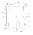
図13は、本発明の第3実施形態に係る光スキャナーに備えられた可動板を説明するための平面図である。
以下、第3実施形態の光スキャナーについて、前述した実施形態の光スキャナーとの相違点を中心に説明し、同様の事項については、その説明を省略する。
第3実施形態の光スキャナーは、可動板の平面視形状が異なる以外は、第1実施形態の光スキャナー1とほぼ同様である。なお、前述した実施形態と同様の構成には、同一符号を付してある。
<Third Embodiment>
Next, a third embodiment of the present invention will be described.
FIG. 13 is a plan view for explaining the movable plate provided in the optical scanner according to the third embodiment of the present invention.
Hereinafter, the optical scanner of the third embodiment will be described focusing on the differences from the optical scanner of the above-described embodiment, and the description of the same matters will be omitted.
The optical scanner of the third embodiment is substantially the same as the
本実施形態の光スキャナーに備えられた可動板21Cは、図13に示すように、本体部212Cと、この本体部212Cから軸線X方向に両側へ突出する1対の突出部213C、214Cと、本体部212から線分Y方向に両側に突出する1対の突出部215C、216Cとで構成されている。これにより、可動板21Cは、平面視にて十字状をなす。
そして、可動板21Cの外周に沿った方向における突出部213Cと突出部215Cとの間には、欠損部251Cが形成されている。また、可動板21Cの外周に沿った方向における突出部213Cと突出部216Cとの間には、欠損部252Cが形成されている。また、可動板21Cの外周に沿った方向における突出部214Cと突出部216Cとの間には、欠損部254Cが形成されている。また、可動板21Cの外周に沿った方向における突出部214Cと突出部215Cとの間には、欠損部253Cが形成されている。
As shown in FIG. 13, the
A missing
本実施形態では、可動板21Cは、板厚方向からの平面視にて軸線Xに対して対称となるように形成されているが、当該平面視にて線分Yに対して非対称となるように形成されている。なお、以下では、欠損部251C、253Cについて代表的に説明するが、欠損部252C、254Cについても同様である。
より具体的に説明すると、欠損部251の線分Y方向に沿った長さをa1とし、欠損部251Cの軸線X方向に沿った長さをb1としたとき、a1<b1の関係を満たす。すなわち、欠損部251Cは、軸線X方向に沿った長さが線分Y方向に沿った長さよりも長い長方形をなしている。これにより、可動板21Cの軸線Xから遠位の端部の質量を効率的に低減することができる。そのため、可動板21Cの回動時の慣性モーメントを効果的に抑えることができる。
In the present embodiment, the movable plate 21C is formed to be symmetric with respect to the axis X in a plan view from the plate thickness direction, but is asymmetric with respect to the line segment Y in the plan view. Is formed. In the following, the missing
More specifically, when the length of the missing
同様に、欠損部253Cの線分Y方向での長さをa3とし、欠損部253Cの軸線X方向での長さをb3としたとき、a3<b3の関係を満たす。すなわち、欠損部253Cは、軸線X方向の長さが線分Y方向での長さよりも長い長方形をなしている。これにより、可動板21Cの軸線Xから遠位の端部の質量を効率的に低減することができる。そのため、可動板21Cの回動時の慣性モーメントを効果的に抑えることができる。
Similarly, when the length of the missing
また、a1>a3、かつ、b1>b3の関係を満たす。これにより、軸線X軸に対して傾斜させて光を光反射部211に入射させる場合に、光反射領域を効率的に確保することができる。
また、この可動板21Cにおいても、可動板21Cの平面視における線分Y方向での長さをAとし、可動板21Cの軸線X方向での長さをBとし、各欠損部251C〜254Cの線分Y方向での長さをaとし、各欠損部251C〜254Cの軸線X方向での長さをbとしたとき、前記式(A)、(B)をそれぞれ満たす。
以上説明したような第3実施形態の光スキャナーによっても、光反射領域を確保しながら可動板の回動時の慣性モーメントを低減するとともに、可動板の寸法精度を簡単に優れたものとすることができる。
Moreover, the relationship of a1> a3 and b1> b3 is satisfied. Thereby, when making it incline with respect to an axis line X-axis and making light inject into the
Also in the movable plate 21C, the length in the line segment Y direction in the plan view of the movable plate 21C is A, the length in the axis X direction of the movable plate 21C is B, and each of the missing
Even with the optical scanner according to the third embodiment as described above, it is possible to reduce the moment of inertia when the movable plate rotates while securing the light reflection area, and to easily improve the dimensional accuracy of the movable plate. Can do.
<第4実施形態>
次に、本発明の第4実施形態について説明する。
図14は、本発明の第4実施形態に係る光スキャナーに備えられた可動板を説明するための平面図である。
以下、第4実施形態の光スキャナーについて、前述した実施形態の光スキャナーとの相違点を中心に説明し、同様の事項については、その説明を省略する。
第4実施形態の光スキャナーは、可動板の平面視形状が異なる以外は、第1実施形態の光スキャナー1とほぼ同様である。なお、前述した実施形態と同様の構成には、同一符号を付してある。
<Fourth embodiment>
Next, a fourth embodiment of the present invention will be described.
FIG. 14 is a plan view for explaining a movable plate provided in an optical scanner according to the fourth embodiment of the present invention.
Hereinafter, the optical scanner according to the fourth embodiment will be described with a focus on differences from the optical scanner according to the above-described embodiment, and description of similar matters will be omitted.
The optical scanner of the fourth embodiment is substantially the same as the
本実施形態の光スキャナーに備えられた可動板21Dは、図14に示すように、本体部212Dと、この本体部212Dから軸線X方向に両側へ突出する1対の突出部213D、214Dと、本体部212から線分Y方向に両側に突出する1対の突出部215D、216Dとで構成されている。これにより、可動板21Dは、平面視にて十字状をなす。
そして、可動板21Dの外周に沿った方向における突出部213Dと突出部215Dとの間には、欠損部251Dが形成されている。また、可動板21Dの外周に沿った方向における突出部213Dと突出部216Dとの間には、欠損部252Dが形成されている。また、可動板21Dの外周に沿った方向における突出部214Dと突出部216Dとの間には、欠損部254Dが形成されている。また、可動板21Dの外周に沿った方向における突出部214Dと突出部215Dとの間には、欠損部253Dが形成されている。
As shown in FIG. 14, the movable plate 21D provided in the optical scanner of the present embodiment includes a
A missing portion 251D is formed between the protruding
本実施形態では、可動板21Dは、平面視にて軸線Xに対して非対称となるように形成され、平面視にて線分Yに対して対称となるように形成されている。なお、以下では、欠損部251D、252Dについて代表的に説明するが、欠損部253D、254Dについても同様である。
また、可動板21Dの平面視における四隅の部分(欠損部251D〜254D)のうち、可動板21Dの回動中心軸(軸線X)に対して一方側(図14中の左側)に位置する2つの部分(欠損部251D、253D)について、a≦bの関係を満たし、可動板21Dの回動中心軸(軸線X)に対して他方側(図14中の右側)に位置する他の2つの部分(欠損部252D、254D)について、b≦aの関係を満たす。これにより、可動板21Dが平面視にて回動中心軸に対して非対称な形状であっても、可動板21Dの重心と可動板21Dの回動中心軸とのズレを抑えることができる。
In the present embodiment, the movable plate 21D is formed so as to be asymmetric with respect to the axis X in plan view, and is formed so as to be symmetric with respect to the line segment Y in plan view. In the following, the missing
Moreover, 2 located in one side (left side in FIG. 14) with respect to the rotation central axis (axis X) of movable plate 21D among the four corner parts (deletion part 251D-254D) in planar view of movable plate 21D. The other two parts (
より具体的に説明すると、欠損部251Dの線分Y方向での長さをa1とし、欠損部251Dの軸線X方向での長さをb1としたとき、a1<b1の関係を満たす。すなわち、欠損部251Dは、軸線X方向の長さが線分Y方向での長さよりも長い長方形をなしている。これにより、可動板21Dの軸線Xから遠位の端部の質量を効率的に低減することができる。そのため、可動板21Dの回動時の慣性モーメントを効果的に抑えることができる。 More specifically, when the length of the missing portion 251D in the line segment Y direction is a1, and the length of the missing portion 251D in the axis X direction is b1, the relationship of a1 <b1 is satisfied. That is, the missing portion 251D has a rectangular shape whose length in the axis line X direction is longer than the length in the line segment Y direction. Thereby, the mass of the end part far from the axis X of the movable plate 21D can be efficiently reduced. Therefore, the moment of inertia when the movable plate 21D is rotated can be effectively suppressed.
一方、欠損部252Dの線分Y方向での長さをa2とし、欠損部252Dの軸線X方向での長さをb2としたとき、a2>b2の関係を満たす。これにより、欠損部252Dの平面視での面積が欠損部251Dの平面視での面積より大きくても、可動板21Dの重心が軸線Xからずれるのを防止または抑制することができる。そのため、可動板21Dの回動を円滑なものとすることができる。なお、本実施形態では、a1×b1<a2×b2の関係を満たす。
また、この可動板21Dにおいても、可動板21Dの平面視における線分Y方向での長さをAとし、可動板21Dの軸線X方向での長さをBとし、各欠損部251D〜254Dの線分Y方向での長さをaとし、各欠損部251D〜254Dの軸線X方向での長さをbとしたとき、前記式(A)、(B)をそれぞれ満たす。
On the other hand, when the length of the missing
Also in this movable plate 21D, the length in the line segment Y direction in the plan view of the movable plate 21D is A, the length in the axis X direction of the movable plate 21D is B, and each of the missing portions 251D to 254D. When the length in the line segment Y direction is a and the length in the axis X direction of each of the missing portions 251D to 254D is b, the above formulas (A) and (B) are satisfied.
以上説明したような第4実施形態の光スキャナーによっても、光反射領域を確保しながら可動板の回動時の慣性モーメントを低減するとともに、可動板の寸法精度を簡単に優れたものとすることができる。
以上説明したような光スキャナーは、例えば、プロジェクター、レーザープリンター、イメージング用ディスプレイ、バーコードリーダー、走査型共焦点顕微鏡などの画像形成装置に好適に適用することができる。その結果、優れた描画特性を有する画像形成装置を提供することができる。
Even with the optical scanner of the fourth embodiment as described above, it is possible to reduce the moment of inertia when the movable plate rotates while ensuring the light reflection area, and to easily improve the dimensional accuracy of the movable plate. Can do.
The optical scanner as described above can be suitably applied to an image forming apparatus such as a projector, a laser printer, an imaging display, a barcode reader, and a scanning confocal microscope. As a result, an image forming apparatus having excellent drawing characteristics can be provided.
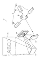
(画像形成装置)
ここで、図15に基づいて、本発明の画像形成装置の一例を説明する。
図15は、本発明の画像形成装置の構成の一例を示す概略図である。なお、以下では、説明の便宜上、スクリーンSCの長手方向を「横方向」といい、長手方向に直角な方向を「縦方向」という。
(Image forming device)
Here, an example of the image forming apparatus of the present invention will be described with reference to FIG.
FIG. 15 is a schematic diagram showing an example of the configuration of the image forming apparatus of the present invention. Hereinafter, for convenience of explanation, the longitudinal direction of the screen SC is referred to as “lateral direction”, and the direction perpendicular to the longitudinal direction is referred to as “vertical direction”.
プロジェクター9は、レーザーなどの光を照出する光源装置91と、クロスダイクロイックプリズム92と、1対の本発明の光スキャナー93、94(例えば、光スキャナー1と同様の構成の光スキャナー)と、固定ミラー95とを有している。
光源装置91は、赤色光を照出する赤色光源装置911と、青色光を照出する青色光源装置912と、緑色光を照出する緑色光源装置913とを備えている。
クロスダイクロイックプリズム92は、4つの直角プリズムを貼り合わせて構成され、赤色光源装置911、青色光源装置912、緑色光源装置913のそれぞれから照出された光を合成する光学素子である。
The
The
The cross
このようなプロジェクター9は、赤色光源装置911、青色光源装置912、緑色光源装置913のそれぞれから、図示しないホストコンピューターからの画像情報に基づいて照出された光をクロスダイクロイックプリズム92で合成し、この合成された光が、光スキャナー93、94によって走査され、さらに固定ミラー95によって反射され、スクリーンSC上でカラー画像を形成するように構成されている。
Such a
ここで、光スキャナー93、94の光走査について具体的に説明する。
まず、クロスダイクロイックプリズム92で合成された光は、光スキャナー93によって横方向に走査される(主走査)。そして、この横方向に走査された光は、光スキャナー94によってさらに縦方向に走査される(副走査)。これにより、2次元カラー画像をスクリーンSC上に形成することができる。このような光スキャナー93、94として本発明の光スキャナーを用いることで、極めて優れた描画特性を発揮することができる。
Here, the optical scanning of the
First, the light combined by the cross
ただし、プロジェクター9としては、光スキャナーにより光を走査し、対象物に画像を形成するように構成されていれば、これに限定されず、例えば、固定ミラー95を省略してもよい。
このように構成されたプロジェクター9によれば、前述した光スキャナー1と同様の構成の光スキャナー93、94を備えるので、安価に、高品位な画像を得ることができる。
However, the
According to the
以上、本発明のアクチュエーター、光スキャナーおよび画像形成装置について、図示の実施形態に基づいて説明したが、本発明はこれに限定されるものではない。例えば、本発明のアクチュエーター、光スキャナーおよび画像形成装置では、各部の構成は、同様の機能を発揮する任意の構成のものに置換することができ、また、任意の構成を付加することもできる。 Although the actuator, optical scanner, and image forming apparatus of the present invention have been described based on the illustrated embodiment, the present invention is not limited to this. For example, in the actuator, the optical scanner, and the image forming apparatus of the present invention, the configuration of each unit can be replaced with an arbitrary configuration that exhibits the same function, and an arbitrary configuration can be added.
また、前述した実施形態では、可動板が平面視において回動中心軸およびそれに垂直な線分の少なくとも一方に対して対称な形状をなす場合を説明したが、これに限定されず、可動板が平面視において回動中心軸およびそれに垂直な線分のいずれに対しても非対称な形状をなしていてもよい。
また、前述した実施形態では、本発明のアクチュエーターを光スキャナーに適用した場合を例に説明したが、本発明のアクチュエーターは、これに限定されず、例えば、光スイッチ、光アッテネータ等の他の光学デバイスに適用することも可能である。
また、前述した実施形態では、可動板を回動させる駆動部がムービングマグネット型の電磁駆動方式を採用した構成を例に説明したが、かかる駆動部は、ムービングコイル型の電磁駆動方式であってもよいし、また、静電駆動方式、圧電駆動方式等の電磁駆動方式以外の駆動方式を採用するものであってもよい。
In the above-described embodiment, the case where the movable plate has a symmetrical shape with respect to at least one of the rotation center axis and a line segment perpendicular to the rotation center axis in plan view has been described. It may have an asymmetric shape with respect to both the rotation center axis and a line segment perpendicular thereto in plan view.
In the above-described embodiments, the case where the actuator of the present invention is applied to an optical scanner has been described as an example. However, the actuator of the present invention is not limited to this, and other optical devices such as an optical switch, an optical attenuator, etc. It can also be applied to devices.
In the above-described embodiment, the driving unit that rotates the movable plate has been described as an example of a moving magnet type electromagnetic driving method. However, the driving unit is a moving coil type electromagnetic driving method. Alternatively, a driving method other than an electromagnetic driving method such as an electrostatic driving method or a piezoelectric driving method may be adopted.
1、1A‥‥光スキャナー 2、2A‥‥基体 3‥‥支持体 4‥‥駆動部 9‥‥プロジェクター 21、21A、21B、21C、21D‥‥可動板 22‥‥支持部 23、23A‥‥連結部 24、24A‥‥連結部 31‥‥凹部 32‥‥板状部 33‥‥枠状部 41‥‥永久磁石 42‥‥コイル 51‥‥窒化膜 52‥‥窒化膜 52A‥‥窒化膜 61‥‥レジスト膜 62‥‥レジスト膜 62A‥‥レジスト膜 71‥‥窒化膜 71A‥‥窒化膜 72‥‥窒化膜 72A‥‥窒化膜 81‥‥レジスト膜 81A‥‥レジスト膜 82‥‥レジスト膜 82A‥‥レジスト膜 91‥‥光源装置 92‥‥クロスダイクロイックプリズム 93‥‥光スキャナー 94‥‥光スキャナー 95‥‥固定ミラー 102‥‥シリコン基板 102A‥‥シリコン基板 211‥‥光反射部 213、213C、213D、214、214C、214D、215、215C、215D、216、216C、216D‥‥突出部 212、212C、212D‥‥本体部 217‥‥溝 218‥‥凹部 231、231A、232A‥‥梁部材 232‥‥梁部材 233‥‥上面 234‥‥下面 235、236‥‥側面 241‥‥梁部材 242‥‥梁部材 251、251C、251D、252、252C、252D、253、253C、253D、254、254C、254D‥‥欠損部 311‥‥底面 521‥‥開口 621‥‥開口 711‥‥開口 712‥‥部分 713‥‥部分 714‥‥開口 721‥‥開口 722‥‥部分 723‥‥部分 724‥‥開口 811‥‥開口 821‥‥開口 911‥‥赤色光源装置 912‥‥青色光源装置 913‥‥緑色光源装置 2311‥‥上面 2312‥‥下面 2313、2314‥‥側面 2315‥‥段差 2316‥‥段差 2321‥‥上面 2322‥‥下面 2323、2324‥‥側面 2325‥‥段差 2326‥‥段差 SC‥‥スクリーン
DESCRIPTION OF
Claims (12)
前記可動部に連結し、かつ前記可動部の回動に伴って捩り変形する連結部と、
前記連結部を支持する支持部と、を有し、
前記可動部は、前記可動部の板厚方向からの平面視にて、前記回動中心軸に対して垂直な方向で両側へ突出する1対の第1突出部と、前記回動中心軸に対して平行な方向で両側に突出する1対の第2突出部とを有する十字状をなし、
前記板厚方向からの平面視における前記回動中心軸に対して垂直な方向の前記可動部の長さをAとし、前記板厚方向からの平面視における前記回動中心軸に対して平行な方向の前記可動部の長さをBとし、前記板厚方向からの平面視における前記回動中心軸に対して垂直な方向の前記第1突出部の長さをaとし、前記板厚方向からの平面視における前記回動中心軸に対して平行な方向の前記第2突出部の長さをbとしたときに、下記式(A)および(B)をそれぞれ満たすことを特徴とするアクチュエーター。
A connecting portion connected to the movable portion and torsionally deformed with the rotation of the movable portion;
A support part for supporting the connecting part,
The movable part includes a pair of first projecting parts projecting to both sides in a direction perpendicular to the pivot center axis in plan view from the plate thickness direction of the movable part, and the pivot center axis. A cross having a pair of second protrusions projecting on both sides in a parallel direction;
The length of the movable portion in a direction perpendicular to the rotation center axis in plan view from the plate thickness direction is A, and is parallel to the rotation center axis in plan view from the plate thickness direction. The length of the movable portion in the direction is B, the length of the first protrusion in the direction perpendicular to the rotation center axis in plan view from the plate thickness direction is a, and from the plate thickness direction An actuator characterized by satisfying the following formulas (A) and (B), respectively, where b is the length of the second projecting portion in the direction parallel to the rotation center axis in plan view:
前記可動部に連結し、かつ前記可動部の回動に伴って捩り変形する連結部と、
前記連結部を支持する支持部と、を有し、
前記可動部は、前記可動部の板厚方向からの平面視にて、前記回動中心軸に沿った1対の辺と前記回動中心軸に対して垂直な方向に沿った1対の辺とで構成された四角形の四隅の部分をそれぞれ四角形に欠いた形状をなし、
前記板厚方向からの平面視における前記回動中心軸に対して垂直な方向の前記可動部の長さをAとし、前記板厚方向からの平面視における前記回動中心軸に対して平行な方向での前記可動部の長さをBとし、前記板厚方向からの平面視における前記四隅の部分の前記回動中心軸に対して垂直な方向の長さをaとし、前記可動部の平面視における前記四隅の部分の前記回動中心軸に対して平行な方向の長さをbとしたときに、下記式(A)および(B)をそれぞれ満たすことを特徴とするアクチュエーター。
A connecting portion connected to the movable portion and torsionally deformed with the rotation of the movable portion;
A support part for supporting the connecting part,
The movable portion includes a pair of sides along the rotation center axis and a pair of sides along a direction perpendicular to the rotation center axis in plan view from the plate thickness direction of the movable portion. Each of the four corners of the quadrangle made up of
The length of the movable portion in a direction perpendicular to the rotation center axis in plan view from the plate thickness direction is A, and is parallel to the rotation center axis in plan view from the plate thickness direction. The length of the movable part in the direction is B, the length in the direction perpendicular to the rotation center axis of the four corners in plan view from the plate thickness direction is a, and the plane of the movable part An actuator characterized by satisfying the following formulas (A) and (B), respectively, where b is a length in a direction parallel to the rotation center axis of the four corner portions when viewed.
前記光反射部を備え、かつ所定の回動中心軸まわりに回動可能な板状の可動部と、
前記可動部に連結し、かつ前記可動部の回動に伴って捩り変形する連結部と、
前記連結部を支持する支持部と、を有し、
前記可動部は、前記可動部の板厚方向からの平面視にて、前記回動中心軸に対して垂直な方向で両側へ突出する1対の第1突出部と、前記回動中心軸に対して平行な方向で両側に突出する1対の第2突出部とを有する十字状をなし、
前記板厚方向からの平面視における前記回動中心軸に対して垂直な方向の前記可動部の長さをAとし、前記板厚方向からの平面視における前記回動中心軸に対して平行な方向の前記可動部の長さをBとし、前記板厚方向からの平面視における前記回動中心軸に対して垂直な方向の前記第1突出部の長さをaとし、前記板厚方向からの平面視における前記回動中心軸に対して平行な方向の前記第2突出部の長さをbとしたときに、下記式(A)および(B)をそれぞれ満たすことを特徴とする光スキャナー。
A plate-like movable part that includes the light reflecting part and is rotatable about a predetermined rotation center axis;
A connecting portion connected to the movable portion and torsionally deformed with the rotation of the movable portion;
A support part for supporting the connecting part,
The movable part includes a pair of first projecting parts projecting to both sides in a direction perpendicular to the pivot center axis in plan view from the plate thickness direction of the movable part, and the pivot center axis. A cross having a pair of second protrusions projecting on both sides in a parallel direction;
The length of the movable portion in a direction perpendicular to the rotation center axis in plan view from the plate thickness direction is A, and is parallel to the rotation center axis in plan view from the plate thickness direction. The length of the movable portion in the direction is B, the length of the first protrusion in the direction perpendicular to the rotation center axis in plan view from the plate thickness direction is a, and from the plate thickness direction An optical scanner characterized by satisfying the following formulas (A) and (B), respectively, where b is the length of the second protrusion in the direction parallel to the rotation center axis in plan view: .
前記光源からの光を走査する光スキャナーと、を備え、
前記光スキャナーは、
光反射性を有する光反射部と、
前記光反射部を備え、かつ所定の回動中心軸まわりに回動可能な板状の可動部と、
前記可動部に連結し、かつ前記可動部の回動に伴って捩り変形する連結部と、
前記連結部を支持する支持部と、を有し、
前記可動部は、前記可動部の板厚方向からの平面視にて、前記回動中心軸に対して垂直な方向で両側へ突出する1対の第1突出部と、前記回動中心軸に対して平行な方向で両側に突出する1対の第2突出部とを有する十字状をなし、
前記板厚方向からの平面視における前記回動中心軸に対して垂直な方向の前記可動部の長さをAとし、前記板厚方向からの平面視における前記回動中心軸に対して平行な方向の前記可動部の長さをBとし、前記板厚方向からの平面視における前記回動中心軸に対して垂直な方向の前記第1突出部の長さをaとし、前記板厚方向からの平面視における前記回動中心軸に対して平行な方向の前記第2突出部の長さをbとしたときに、下記式(A)および(B)をそれぞれ満たすことを特徴とする画像形成装置。
An optical scanner that scans the light from the light source,
The optical scanner is
A light reflecting portion having light reflectivity;
A plate-like movable part that includes the light reflecting part and is rotatable about a predetermined rotation center axis;
A connecting portion connected to the movable portion and torsionally deformed with the rotation of the movable portion;
A support part for supporting the connecting part,
The movable part includes a pair of first projecting parts projecting to both sides in a direction perpendicular to the pivot center axis in plan view from the plate thickness direction of the movable part, and the pivot center axis. A cross having a pair of second protrusions projecting on both sides in a parallel direction;
The length of the movable portion in a direction perpendicular to the rotation center axis in plan view from the plate thickness direction is A, and is parallel to the rotation center axis in plan view from the plate thickness direction. The length of the movable portion in the direction is B, the length of the first protrusion in the direction perpendicular to the rotation center axis in plan view from the plate thickness direction is a, and from the plate thickness direction An image formation characterized by satisfying the following formulas (A) and (B), where b is the length of the second protrusion in the direction parallel to the rotation center axis in a plan view: apparatus.
Priority Applications (2)
| Application Number | Priority Date | Filing Date | Title |
|---|---|---|---|
| JP2011084841A JP2012220641A (en) | 2011-04-06 | 2011-04-06 | Actuator, optical scanner and image forming device |
| US13/439,239 US8614831B2 (en) | 2011-04-06 | 2012-04-04 | Actuator and optical scanner |
Applications Claiming Priority (1)
| Application Number | Priority Date | Filing Date | Title |
|---|---|---|---|
| JP2011084841A JP2012220641A (en) | 2011-04-06 | 2011-04-06 | Actuator, optical scanner and image forming device |
Publications (2)
| Publication Number | Publication Date |
|---|---|
| JP2012220641A true JP2012220641A (en) | 2012-11-12 |
| JP2012220641A5 JP2012220641A5 (en) | 2014-05-15 |
Family
ID=46965927
Family Applications (1)
| Application Number | Title | Priority Date | Filing Date |
|---|---|---|---|
| JP2011084841A Withdrawn JP2012220641A (en) | 2011-04-06 | 2011-04-06 | Actuator, optical scanner and image forming device |
Country Status (2)
| Country | Link |
|---|---|
| US (1) | US8614831B2 (en) |
| JP (1) | JP2012220641A (en) |
Families Citing this family (1)
| Publication number | Priority date | Publication date | Assignee | Title |
|---|---|---|---|---|
| JP5842356B2 (en) * | 2011-03-24 | 2016-01-13 | セイコーエプソン株式会社 | Actuator, optical scanner and image forming apparatus |
Citations (3)
| Publication number | Priority date | Publication date | Assignee | Title |
|---|---|---|---|---|
| JP2003131161A (en) * | 2001-07-11 | 2003-05-08 | Canon Inc | Optical deflector and its manufacturing method, optical equipment using the same, and torsion oscillating member |
| JP2009089501A (en) * | 2007-09-28 | 2009-04-23 | Nippon Signal Co Ltd:The | Planar electromagnetic actuator |
| JP2011128203A (en) * | 2009-12-15 | 2011-06-30 | Toyota Central R&D Labs Inc | Optical device |
Family Cites Families (7)
| Publication number | Priority date | Publication date | Assignee | Title |
|---|---|---|---|---|
| JP4641378B2 (en) * | 2004-02-16 | 2011-03-02 | キヤノン株式会社 | Optical scanning device and image display device having the same |
| JP4193817B2 (en) * | 2005-06-22 | 2008-12-10 | セイコーエプソン株式会社 | Actuator |
| JP2009069675A (en) | 2007-09-14 | 2009-04-02 | Ricoh Co Ltd | Optical scanner, optical scanning device, image forming apparatus and method of manufacturing optical scanner |
| JP2009148847A (en) | 2007-12-19 | 2009-07-09 | Canon Inc | Manufacturing method for structure by anisotropic etching and silicon substrate with etching mask |
| JP2011170370A (en) | 2008-03-13 | 2011-09-01 | Seiko Epson Corp | Optical deflector and method of manufacturing the same |
| JP5521359B2 (en) | 2008-03-13 | 2014-06-11 | セイコーエプソン株式会社 | Optical deflector and manufacturing method thereof |
| JP2011107675A (en) | 2009-10-20 | 2011-06-02 | Seiko Epson Corp | Light deflecting element, light deflector and image forming device |
-
2011
- 2011-04-06 JP JP2011084841A patent/JP2012220641A/en not_active Withdrawn
-
2012
- 2012-04-04 US US13/439,239 patent/US8614831B2/en active Active
Patent Citations (3)
| Publication number | Priority date | Publication date | Assignee | Title |
|---|---|---|---|---|
| JP2003131161A (en) * | 2001-07-11 | 2003-05-08 | Canon Inc | Optical deflector and its manufacturing method, optical equipment using the same, and torsion oscillating member |
| JP2009089501A (en) * | 2007-09-28 | 2009-04-23 | Nippon Signal Co Ltd:The | Planar electromagnetic actuator |
| JP2011128203A (en) * | 2009-12-15 | 2011-06-30 | Toyota Central R&D Labs Inc | Optical device |
Also Published As
| Publication number | Publication date |
|---|---|
| US8614831B2 (en) | 2013-12-24 |
| US20120257261A1 (en) | 2012-10-11 |
Similar Documents
| Publication | Publication Date | Title |
|---|---|---|
| JP5842356B2 (en) | Actuator, optical scanner and image forming apparatus | |
| JP5842369B2 (en) | Actuator manufacturing method, optical scanner manufacturing method and image forming apparatus manufacturing method, actuator, optical scanner and image forming apparatus | |
| JP5909862B2 (en) | Actuator, optical scanner and image forming apparatus | |
| US8988750B2 (en) | Optical scanner, mirror chip, method of manufacturing optical scanner, and image forming apparatus | |
| JP2005128147A (en) | Optical deflector and optical apparatus using the same | |
| JP5333286B2 (en) | Optical scanner and image forming apparatus | |
| JP5834431B2 (en) | Actuator, actuator manufacturing method, optical scanner, and image forming apparatus | |
| JP5640687B2 (en) | Actuator, actuator manufacturing method, optical scanner, and image forming apparatus | |
| US8928962B2 (en) | Optical device, method for manufacturing optical device, and optical scanner | |
| JP2012220641A (en) | Actuator, optical scanner and image forming device | |
| JP5842837B2 (en) | Actuator, optical scanner and image forming apparatus | |
| JP6003025B2 (en) | Actuator, optical scanner and image forming apparatus | |
| JP5909914B2 (en) | Actuator, optical scanner and image forming apparatus | |
| JP5354162B2 (en) | Optical device, optical scanner, and image forming apparatus | |
| JP2011048229A (en) | Optical scanner and image forming apparatus | |
| JP5168735B2 (en) | Optical device, optical scanner, and image forming apparatus |
Legal Events
| Date | Code | Title | Description |
|---|---|---|---|
| A521 | Request for written amendment filed |
Free format text: JAPANESE INTERMEDIATE CODE: A523 Effective date: 20140402 |
|
| A621 | Written request for application examination |
Free format text: JAPANESE INTERMEDIATE CODE: A621 Effective date: 20140402 |
|
| A977 | Report on retrieval |
Free format text: JAPANESE INTERMEDIATE CODE: A971007 Effective date: 20150121 |
|
| A131 | Notification of reasons for refusal |
Free format text: JAPANESE INTERMEDIATE CODE: A131 Effective date: 20150127 |
|
| A521 | Request for written amendment filed |
Free format text: JAPANESE INTERMEDIATE CODE: A523 Effective date: 20150325 |
|
| A131 | Notification of reasons for refusal |
Free format text: JAPANESE INTERMEDIATE CODE: A131 Effective date: 20150901 |
|
| A761 | Written withdrawal of application |
Free format text: JAPANESE INTERMEDIATE CODE: A761 Effective date: 20151020 |