JP2009217193A - Optical deflector and method of manufacturing the same - Google Patents
Optical deflector and method of manufacturing the same Download PDFInfo
- Publication number
- JP2009217193A JP2009217193A JP2008063522A JP2008063522A JP2009217193A JP 2009217193 A JP2009217193 A JP 2009217193A JP 2008063522 A JP2008063522 A JP 2008063522A JP 2008063522 A JP2008063522 A JP 2008063522A JP 2009217193 A JP2009217193 A JP 2009217193A
- Authority
- JP
- Japan
- Prior art keywords
- magnet
- mirror
- optical deflector
- substrate
- recess
- Prior art date
- Legal status (The legal status is an assumption and is not a legal conclusion. Google has not performed a legal analysis and makes no representation as to the accuracy of the status listed.)
- Withdrawn
Links
Images


Abstract
Description
本発明は、MEMS(Micro Electro Mechanical System)技術を用いた光偏向器及びその駆動方法に関する。 The present invention relates to an optical deflector using MEMS (Micro Electro Mechanical System) technology and a driving method thereof.
近年、MEMS技術を用いたマイクロアクチュエータの開発が盛んである。例えば、一対の弾性支持部(トーションバー)でねじり回転可能に支持されたミラーを備えた光偏向器は、簡便な構成で画像表示装置を形成することが可能なデバイスとして開発が進んでいる。 In recent years, development of microactuators using MEMS technology has been active. For example, an optical deflector including a mirror supported to be torsionally rotated by a pair of elastic support portions (torsion bars) has been developed as a device capable of forming an image display device with a simple configuration.
このようなミラーを駆動する方法としては、静電引力を利用した方式、電磁力を利用した方式、圧電素子を利用した方式が主に挙げられる。 As a method for driving such a mirror, a method using electrostatic attraction, a method using electromagnetic force, and a method using a piezoelectric element are mainly cited.
このうち、電磁力を利用した光偏向器では、ミラーの反射面の裏面側に、ミラーを回動させる駆動力を与えるための磁石が接合される(特許文献1参照)。
ところで、ミラーの高速動作時の歪み(動撓み)を抑制するためには、ミラーの剛性が高いことが好ましい。ミラーの剛性を高くするにはミラーを厚くすればよいが、この場合には、駆動トルクが上昇することが懸念される。したがって、駆動トルクの上昇を抑えるために慣性モーメントをできるだけ減らしつつ、ミラーの剛性を維持して動撓みを抑制する構造が求められている。 By the way, in order to suppress distortion (dynamic deflection) during high-speed operation of the mirror, it is preferable that the mirror has high rigidity. In order to increase the rigidity of the mirror, the thickness of the mirror may be increased. In this case, however, there is a concern that the driving torque increases. Therefore, there is a need for a structure that suppresses dynamic deflection while maintaining the rigidity of the mirror while reducing the moment of inertia as much as possible in order to suppress the increase in drive torque.
本発明は、上記の事情に鑑みてなされたものであり、その目的の一つは、ミラーの慣性モーメントをできるだけ減らしつつ、ミラーの剛性を維持して動撓みを抑制できる光偏向器及びその製造方法を提供することにある。 The present invention has been made in view of the above circumstances, and one of its purposes is an optical deflector capable of suppressing dynamic deflection while maintaining the rigidity of the mirror while reducing the moment of inertia of the mirror as much as possible, and its manufacture. To provide a method.
上記の目的を達成するため、本発明の光偏向器は、所定の軸に沿って回動可能に構成された、反射面を備えるミラーと、ミラーの反射面の裏面に形成された磁石配置用の窪みと、ミラーの窪みに固定された磁石と、を有する。 In order to achieve the above object, an optical deflector according to the present invention is a mirror having a reflecting surface configured to be rotatable along a predetermined axis, and a magnet arrangement formed on the back surface of the reflecting surface of the mirror. And a magnet fixed to the mirror recess.
上記構成では、磁石は磁石配置用の窪みに固定されていることから、窪みがない場合に比べて、ミラーの重心が回動の中心軸に近づくことになる。このように、ミラーの重心を回動の中心軸に近づけることにより、ミラーの慣性モーメントが減少する。また、窪みが形成された箇所には磁石が配置されていることから、この磁石により窪みの部位が補強され、全体としてミラーの剛性は維持される。 In the above configuration, since the magnet is fixed to the recess for arranging the magnet, the center of gravity of the mirror is closer to the center axis of the rotation than when there is no recess. Thus, by bringing the center of gravity of the mirror closer to the center axis of rotation, the moment of inertia of the mirror is reduced. Moreover, since the magnet is arrange | positioned in the location in which the hollow was formed, the hollow part is reinforced by this magnet and the rigidity of a mirror is maintained as a whole.
磁石は、磁石の側面に形成された接着剤によりミラーに接合されていることが好ましい。このように、磁石とミラーの間には接着剤を設けないことにより、接着剤に起因する磁石の傾きや位置ずれが防止される。また、磁石とミラーの間の全面に接着剤を塗布する場合と比較して、硬化する際に生じる応力が低減され、ミラーの撓みが抑制される。 The magnet is preferably bonded to the mirror by an adhesive formed on the side surface of the magnet. Thus, by not providing an adhesive between the magnet and the mirror, the inclination and displacement of the magnet due to the adhesive can be prevented. Moreover, compared with the case where an adhesive is applied to the entire surface between the magnet and the mirror, the stress generated during curing is reduced, and the bending of the mirror is suppressed.
さらに、上記の目的を達成するため、本発明の光偏向器の製造方法は、基板のミラーとなる部位の裏面に磁石配置用の窪みを形成する工程と、基板の窪みに磁石を固定する工程と、を有する。 Furthermore, in order to achieve the above object, the method of manufacturing an optical deflector according to the present invention includes a step of forming a magnet placement recess on the back surface of a portion to be a mirror of the substrate, and a step of fixing the magnet in the recess of the substrate And having.
上記構成では、磁石配置用の窪みは磁石の固定のためのアライメントマークとしても機能するため、正確な磁石の固定が可能となる。また、磁石は磁石配置用の窪みに固定されていることから、窪みがない場合に比べて、ミラーの重心が回動の中心軸に近づくことになる。このように、ミラーの重心を回動の中心軸に近づけることにより、ミラーの慣性モーメントが減少する。また、窪みが形成された箇所には磁石が配置されていることから、この磁石により窪みの部位が補強され、全体としてミラーの剛性は維持される。 In the above configuration, since the recess for magnet arrangement also functions as an alignment mark for fixing the magnet, it is possible to fix the magnet accurately. In addition, since the magnet is fixed to the recess for arranging the magnet, the center of gravity of the mirror is closer to the central axis of rotation than when there is no recess. Thus, by bringing the center of gravity of the mirror closer to the center axis of rotation, the moment of inertia of the mirror is reduced. Moreover, since the magnet is arrange | positioned in the location in which the hollow was formed, the hollow part is reinforced by this magnet and the rigidity of a mirror is maintained as a whole.
好ましくは、基板の両面に所定のパターンをもつマスクを形成する工程と、マスクを用いて基板を両面からエッチングすることにより、基板をミラー形状に加工する工程と、をさらに有し、基板をミラー形状に加工する工程と同時に、磁石配置用の窪みを形成する。これにより、窪みを設けない場合に比べて、工程を増加させずに、磁石配置用の窪みが形成される。 Preferably, the method further includes a step of forming a mask having a predetermined pattern on both sides of the substrate and a step of processing the substrate into a mirror shape by etching the substrate from both sides using the mask. Simultaneously with the step of processing into a shape, a recess for magnet placement is formed. Thereby, compared with the case where a hollow is not provided, the hollow for magnet arrangement | positioning is formed, without increasing a process.
好ましくは、基板の窪みに磁石を固定する工程は、基板の窪みに磁石を載置する工程と、磁石の外縁における基板の裏面上に接着剤を塗布して、基板の裏面と磁石の側面とを接合する工程と、を有する。このように、磁石とミラーの間には接着剤を設けないことにより、接着剤に起因する磁石の傾きや位置ずれが防止される。また、磁石とミラーの間の全面に接着剤を塗布する場合と比較して、硬化する際に生じる応力が低減され、ミラーの撓みが抑制される。 Preferably, the step of fixing the magnet in the recess of the substrate includes the step of placing the magnet in the recess of the substrate, applying an adhesive on the back surface of the substrate at the outer edge of the magnet, And joining. Thus, by not providing an adhesive between the magnet and the mirror, the inclination and displacement of the magnet due to the adhesive can be prevented. Moreover, compared with the case where an adhesive is applied to the entire surface between the magnet and the mirror, the stress generated during curing is reduced, and the bending of the mirror is suppressed.
(第1実施形態)
以下に、本発明の実施の形態について、図面を参照して説明する。
図1は、本実施形態に係る光偏向器の構成を示す平面図である。図2は、図1のII−II線における断面図である。
(First embodiment)
Embodiments of the present invention will be described below with reference to the drawings.
FIG. 1 is a plan view showing the configuration of the optical deflector according to the present embodiment. 2 is a cross-sectional view taken along line II-II in FIG.
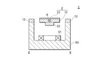
光偏向器1は、可動板11と、支持枠12と、可動板11を支持枠12に対してねじり回転可能に支持する一対の弾性支持部13とを有する。可動板11、支持枠12、及び弾性支持部13は、例えば、シリコン基板をエッチング加工することにより一体形成される。可動板11の表面には、反射膜21が形成されている。これにより、可動板11及び反射膜21からなるミラー2が構成される。
The
また、可動板11の裏面には、磁石22が接合されている。磁石22は、可動板11を平面視したときに、可動板11の回転中心軸である軸線Xに直交する方向に磁化されている。すなわち、磁石22は、軸線Xを介して対向する互いに極性の異なる一対の磁極を有している。支持枠12は、ホルダ50に接合されており、ホルダ50上には、可動板11を駆動させるためのコイル51が配置されている。
A
上記の振動ミラー1では、周期的に変化する電流(交流)がコイル51に供給される。これにより、コイル51は上方(可動板11側)に向く磁界と、下方に向く磁界とを交互に発生させる。これにより、コイル51に対し磁石22の一対の磁極のうち一方の磁極が接近し他方の磁極が離間するようにして、弾性支持部13を捩れ変形させながら、可動板11がX軸回りに回動させられる。
In the oscillating
図3は、可動板11の裏面図である。また、図4は、可動板11および磁石22の接合の様子を示す断面図である。
FIG. 3 is a rear view of the
図3に示すように、多角形又は円形に近い平面外形をもつ可動板11の中心に、磁石22が配置されている。そして、図4に示すように、可動板11の裏面には、磁石配置用の窪み14が形成されており、この窪み14に磁石22が固定されている。窪み14の深さに限定はないが、少なくとも窪み14の部位における可動板11と磁石22の合計厚さが、窪み14以外の部位における可動板11の厚さと同等以上であればよい。これにより、窪み14の部位の剛性が、他の部位に比べて低くなることが防止される。
As shown in FIG. 3, the
可動板11への磁石22の固定方法に限定はないが、好ましくは、磁石22の側面に接着剤23が塗布されており、これにより、可動板11の裏面と磁石22の側面とが接合されている。接着剤23は、熱硬化性接着剤、紫外線硬化性接着剤等の各種の接着剤を使用することができる。例えば、接着剤23は、磁石22の側面に部分的に複数箇所に塗布しても、磁石22の全ての側面を覆う枠状に塗布してもよい。
The method of fixing the
次に、上記の本実施形態に係る光偏向器1の製造方法について、図5〜図20を参照して説明する。
Next, a method for manufacturing the
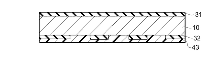
図5に示すように、例えば、シリコンからなる基板10を用意する。そして、図6に示すように、熱酸化により、基板10の両面に酸化シリコンからなるマスク31,32を形成する。
As shown in FIG. 5, for example, a
次に、図7に示すように、基板10の表面側のマスク31上にレジスト41を形成する。レジストは、ポジ型であってもネガ型であってもよい。そして、続いて、図8に示すように、基板10の裏面側のマスク32上にレジスト42を形成する。
Next, as shown in FIG. 7, a
次に、図9に示すように、基板10の裏面側のレジスト42を露光及び現像して、レジスト42に所定の開口パターンP2,P2’を形成する。開口パターンP2は、可動板11、支持枠12、弾性支持部13以外の領域を開口するパターンである。開口パターンP2’は、窪み14を開口するパターンである。
Next, as shown in FIG. 9, the
次に、図10に示すように、レジスト42をマスクとして裏面側のマスク32をエッチングする。これにより、レジスト42の開口パターンP2,P2’が、マスク32に転写される。マスク32のエッチングには、例えばバッファードフッ酸(BHF)が用いられる。
Next, as shown in FIG. 10, the
次に、図11に示すように、基板両面のレジスト41,42を除去する。レジスト41,42の除去には、硫酸洗浄又はアッシングが用いられる。 Next, as shown in FIG. 11, the resists 41 and 42 on both sides of the substrate are removed. For removing the resists 41 and 42, sulfuric acid washing or ashing is used.
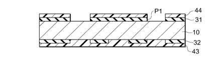
次に、図12に示すように、基板10の裏面側に再度、レジスト43を形成する。さらに、図13に示すように、基板10の表面側に再度、レジスト44を形成する。
Next, as shown in FIG. 12, a resist 43 is formed again on the back side of the
次に、図14に示すように、基板10の表面側のレジスト44を露光及び現像して、レジスト44に所定の開口パターンP1を形成する。開口パターンP1は、可動板11、支持枠12、弾性支持部13以外の領域を開口するパターンである。レジスト44は、窪み14に対応する領域を覆っている。
Next, as shown in FIG. 14, the resist 44 on the surface side of the
次に、図15に示すように、レジスト44をマスクとして表面側のマスク31をエッチングする。これにより、レジスト44の開口パターンP1が、マスク31に転写される。マスク31のエッチングには、例えばバッファードフッ酸(BHF)が用いられる。
Next, as shown in FIG. 15, the
次に、図16に示すように、基板両面のレジスト43,44を除去する。レジスト43,44の除去には、硫酸洗浄又はアッシングが用いられる。 Next, as shown in FIG. 16, the resists 43 and 44 on both surfaces of the substrate are removed. For removing the resists 43 and 44, sulfuric acid cleaning or ashing is used.
次に、図17に示すように、マスク31,32を用いて、基板10をエッチングする。これにより、開口パターンP1、P2の領域においては、基板10は両面からエッチングされて、基板10に貫通孔が形成され、可動板11、支持枠12、弾性支持部13のパターンが形成される。また、開口パターンP2’の領域においては、基板10は裏面のみからエッチングされて、貫通孔ではなく窪み14が形成される。基板10のエッチングには、ドライエッチング又はウェットエッチングのいずれも適用可能であるが、例えば、KOHを用いたウェットエッチングを用いる。Siの面方位(100)ウェハからなる基板10に、KOHなどのウェットエッチングを施した場合には、窪み14の側面にはSiの(111)面が現れることから、窪み14の側面はテーパー形状となる。窪み14の側面がテーパー形状となることで、窪み14への磁石22の配置、及び窪み14への接着剤23の収容が可能となる。
Next, as shown in FIG. 17, the
次に、図18に示すように、マスク31,32を除去した後、さらに、基板10の表面に金属膜を成膜しパターニングすることにより、可動板11上に反射膜21を形成する。金属膜の成膜方法としては、真空蒸着、スパッタリング、電気メッキ、無電解メッキ、金属箔の接合等が挙げられる。なお、マスク31及びマスク32を除去せずに、残しておいてもよい。
Next, as shown in FIG. 18, after removing the
次に、図19に示すように、可動板11の窪み14に磁石22を載置する。続いて、図20に示すように、磁石22の外縁における窪み14内に接着剤23を塗布し、接着剤23を硬化させることにより、磁石22の側面と可動板11の裏面とを接合させる。
Next, as shown in FIG. 19, the
以降の工程としては、このようにして一枚の基板を用いて作製された可動板11、支持枠12、弾性支持部13を含む構造体を、ホルダ50に取り付けることにより、光偏向器1が製造される。
As the subsequent steps, the
上記の本実施形態に係る光偏向器1及びその製造方法では、磁石22は磁石配置用の窪み14に固定されていることから、窪み14がない場合に比べて、ミラー2の重心が回動の中心軸に近づくことになる。回動の中心軸は、弾性支持部13により規定される。このように、ミラーの重心を回動の中心軸に近づけることにより、ミラーの慣性モーメントが減少する。慣性モーメントを減少できることにより、駆動トルクの増加が抑制される。また、窪みが形成された箇所には磁石が配置されていることから、この磁石により窪みの部位が補強され、全体としてミラーの剛性は維持される。ミラーの剛性が高く維持されることにより、動撓みが抑制される。さらに、磁石配置用の窪みは磁石の固定のためのアライメントマークとしても機能するため、磁石の配置精度が向上する。
In the
さらに、本実施形態では、接着剤23により可動板11の裏面と磁石22の側面とが接合される。このように、磁石22と可動板11の間に接着剤23を設けないことにより、接着剤23に起因する磁石の傾きや位置ずれが防止される。また、磁石22と可動板11の間の全面に接着剤を塗布する場合と比較して、硬化する際に生じる応力が低減され、可動板11の撓みが抑制される。
Furthermore, in this embodiment, the back surface of the
さらに、本実施形態に係る光偏向器の製造方法では、窪み14を設けない場合に比べて、工程を追加することなく、可動板11の裏面に窪み14を設けることができる。
Furthermore, in the manufacturing method of the optical deflector according to the present embodiment, it is possible to provide the
(第2実施形態)
本実施形態に係る光偏向器1の応用例として、投射型の表示装置を説明する。図21は、投射型の表示装置の概略構成を示す図である。図21に示す光走査装置は、水平走査ミラーとして図1に示す光偏向器1を用いている。
(Second Embodiment)
As an application example of the
図21に示す光走査装置は、光偏向器1の他に、レーザ光源101と、ダイクロイックミラー102と、フォトダイオード103と、垂直ミラー104とを備える。
The optical scanning device shown in FIG. 21 includes a
レーザ光源101は、赤色レーザ光を出射する赤色レーザ光源101Rと、青色レーザ光を出射する青色レーザ光源101Bと、緑色レーザ光を出射する緑色レーザ光源101Gとを有する。ただし、2色以下又は4色以上のレーザ光源を用いてもよい。
The
ダイクロイックミラー102は、赤色レーザ光源101Rからの赤色レーザ光を反射するダイクロイックミラー102Rと、青色レーザ光を反射し赤色レーザ光を透過させるダイクロイックミラー102Bと、緑色レーザ光を反射し青色レーザ光及び赤色レーザ光を透過させるダイクロイックミラー102Gとを有する。この3種のダイクロイックミラー102により、赤色レーザ光、青色レーザ光、及び緑色レーザ光の合成光が振動ミラー1に入射する。
The dichroic mirror 102 includes a dichroic mirror 102R that reflects red laser light from the red laser light source 101R, a
フォトダイオード103は、各ダイクロイックミラー102R,102G,102Bに反射されずに透過した赤色レーザ光、緑色レーザ光、青色レーザ光の光量を検出する。
The
光偏向器1は、ダイクロイックミラー102から送られたレーザ光を水平方向(軸線Xの垂直方向)に走査する。光偏向器1は、上述したように、MEMSにより形成された、共振型ミラーである。
The
垂直ミラー104は、光偏向器1により反射されたレーザ光を垂直方向に走査する。垂直ミラー104は、例えば、ガルバノミラーにより構成される。ガルバノミラーとはミラーに軸を付け、電気振動に応じてミラーの回転角を変えられるようにした偏向器である。光偏向器1によるレーザ光の水平走査、及び垂直ミラー104によるレーザ光の垂直走査により画像が表示される。
The
本実施形態に係る光走査装置は、上記のレーザ光源101、振動ミラー1、垂直ミラー104の駆動制御系として、さらに、レーザ光源101を駆動するレーザ駆動手段110と、光偏向器1を駆動する水平ミラー駆動手段111と、垂直ミラー104を駆動する垂直ミラー駆動手段112と、全体の動作の制御を担う制御手段113と、記憶手段114とを有する。
The optical scanning device according to the present embodiment further drives a
制御手段113は、パーソナルコンピュータや携帯電話等の各種の映像ソース115から送られた画像情報に基づいて、これらの画像を表示すべく、レーザ駆動手段110、水平ミラー駆動手段111、垂直ミラー駆動手段112の動作を制御する。
The control means 113 is based on image information sent from
記憶手段114は、例えば、各種のプログラムを収納するROMと、変数等を収納するRAMと、不揮発性メモリとにより構成される。
The
本実施形態に係る光偏向器1を表示装置に適用することにより、表示性能の良好な表示装置を実現できる。
By applying the
本発明は、上記の実施形態の説明に限定されない。
例えば、可動板11は円形以外の多角形でもよい。また、本実施形態では、1次元1自由度で駆動するタイプの可動板11を例示したが、2次元に駆動するタイプの可動板11であってもよく、また、1次元2自由度で駆動するタイプの可動板11であってもよい。2次元に駆動するタイプの振動ミラーを用いた場合には、垂直ミラー104は不要である。磁石22の側面ではなく、磁石22の底面に接着剤23を塗布してもよい。
また、光偏向器1は、表示装置以外にもレーザプリンタ等に適用可能である。
その他、本発明の要旨を逸脱しない範囲で、種々の変更が可能である。
The present invention is not limited to the description of the above embodiment.
For example, the
The
In addition, various modifications can be made without departing from the scope of the present invention.
1…光偏向器、2…ミラー、10…基板、11…可動板、12…支持枠、13…弾性支持部、14…窪み、50…ホルダ、21…反射膜、22…磁石、23…接着剤、31,32…マスク、41,42,43,44…レジスト、50…ホルダ、51…コイル、100…表示装置、101…レーザ光源、101R…赤色レーザ光源、101G…緑色レーザ光源、101B…青色レーザ光源、102,102R,102G,102B…ダイクロイックミラー、103,103R,103G,103B…フォトダイオード、104…垂直ミラー、110…レーザ駆動手段、111…水平ミラー駆動手段、112…垂直ミラー駆動手段、113…制御手段、114…記憶手段、115…映像ソース、P1、P2…開口パターン
DESCRIPTION OF
Claims (5)
前記ミラーの前記反射面の裏面に形成された磁石配置用の窪みと、
前記ミラーの前記窪みに固定された磁石と、
を有する光偏向器。 A mirror having a reflecting surface, configured to be rotatable along a predetermined axis;
A recess for magnet arrangement formed on the back surface of the reflecting surface of the mirror;
A magnet fixed in the recess of the mirror;
An optical deflector.
請求項1記載の光偏向器。 The magnet is joined to the mirror by an adhesive formed on a side surface of the magnet.
The optical deflector according to claim 1.
前記基板の前記窪みに磁石を固定する工程と、
を有する光偏向器の製造方法。 Forming a recess for magnet placement on the back surface of the portion to be a mirror of the substrate;
Fixing a magnet in the recess of the substrate;
The manufacturing method of the optical deflector which has.
前記マスクを用いて前記基板を両面からエッチングすることにより、前記基板をミラー形状に加工する工程と、をさらに有し、
前記基板をミラー形状に加工する工程と同時に、前記磁石配置用の窪みを形成する、
請求項3記載の光偏向器の製造方法。 Forming a mask having a predetermined pattern on both sides of the substrate;
Further processing the substrate into a mirror shape by etching the substrate from both sides using the mask,
Simultaneously with the step of processing the substrate into a mirror shape, the recess for magnet placement is formed.
The manufacturing method of the optical deflector of Claim 3.
前記基板の前記窪みに磁石を載置する工程と、
前記磁石の外縁における前記基板の裏面上に接着剤を塗布して、前記基板の裏面と前記磁石の側面とを接合する工程と、
を有する請求項3記載の光偏向器の製造方法。 The step of fixing a magnet in the depression of the substrate includes
Placing a magnet in the recess of the substrate;
Applying an adhesive on the back surface of the substrate at the outer edge of the magnet, and joining the back surface of the substrate and the side surface of the magnet;
The method of manufacturing an optical deflector according to claim 3.
Priority Applications (1)
| Application Number | Priority Date | Filing Date | Title |
|---|---|---|---|
| JP2008063522A JP2009217193A (en) | 2008-03-13 | 2008-03-13 | Optical deflector and method of manufacturing the same |
Applications Claiming Priority (1)
| Application Number | Priority Date | Filing Date | Title |
|---|---|---|---|
| JP2008063522A JP2009217193A (en) | 2008-03-13 | 2008-03-13 | Optical deflector and method of manufacturing the same |
Publications (2)
| Publication Number | Publication Date |
|---|---|
| JP2009217193A true JP2009217193A (en) | 2009-09-24 |
| JP2009217193A5 JP2009217193A5 (en) | 2011-04-07 |
Family
ID=41189070
Family Applications (1)
| Application Number | Title | Priority Date | Filing Date |
|---|---|---|---|
| JP2008063522A Withdrawn JP2009217193A (en) | 2008-03-13 | 2008-03-13 | Optical deflector and method of manufacturing the same |
Country Status (1)
| Country | Link |
|---|---|
| JP (1) | JP2009217193A (en) |
Cited By (3)
| Publication number | Priority date | Publication date | Assignee | Title |
|---|---|---|---|---|
| WO2012127858A1 (en) * | 2011-03-24 | 2012-09-27 | セイコーエプソン株式会社 | Actuator, optical scanner, and image generator |
| JP2013084011A (en) * | 2013-01-30 | 2013-05-09 | Seiko Epson Corp | Actuator, optical scanner, and image forming apparatus |
| JP2013101199A (en) * | 2011-11-08 | 2013-05-23 | Seiko Epson Corp | Mirror device, optical scanner and image formation apparatus |
-
2008
- 2008-03-13 JP JP2008063522A patent/JP2009217193A/en not_active Withdrawn
Cited By (5)
| Publication number | Priority date | Publication date | Assignee | Title |
|---|---|---|---|---|
| WO2012127858A1 (en) * | 2011-03-24 | 2012-09-27 | セイコーエプソン株式会社 | Actuator, optical scanner, and image generator |
| JP2012203149A (en) * | 2011-03-24 | 2012-10-22 | Seiko Epson Corp | Actuator, optical scanner and image forming apparatus |
| RU2566738C2 (en) * | 2011-03-24 | 2015-10-27 | Сейко Эпсон Корпорейшн | Actuating mechanism, optical scanner and imager |
| JP2013101199A (en) * | 2011-11-08 | 2013-05-23 | Seiko Epson Corp | Mirror device, optical scanner and image formation apparatus |
| JP2013084011A (en) * | 2013-01-30 | 2013-05-09 | Seiko Epson Corp | Actuator, optical scanner, and image forming apparatus |
Similar Documents
| Publication | Publication Date | Title |
|---|---|---|
| JP5521359B2 (en) | Optical deflector and manufacturing method thereof | |
| JP5146204B2 (en) | Optical device, optical scanner, and image forming apparatus | |
| JP6349229B2 (en) | Biaxial optical deflector and manufacturing method thereof | |
| JP5655365B2 (en) | Optical deflector, optical deflector manufacturing method, and image display apparatus | |
| TW201239393A (en) | Actuator, optical scanner, and image forming apparatus | |
| JP5333286B2 (en) | Optical scanner and image forming apparatus | |
| JP2010085880A (en) | Optical deflector and method for manufacturing optical deflector | |
| US20120257268A1 (en) | Actuator, optical scanner, and image forming apparatus | |
| JP2009217193A (en) | Optical deflector and method of manufacturing the same | |
| JP5640687B2 (en) | Actuator, actuator manufacturing method, optical scanner, and image forming apparatus | |
| JP5915100B2 (en) | Mirror device, mirror device manufacturing method, optical scanner, and image forming apparatus | |
| JP2011170370A (en) | Optical deflector and method of manufacturing the same | |
| JP2012123117A (en) | Actuator, optical scanner and image forming device | |
| JP5387222B2 (en) | Optical deflector | |
| JP2012108164A (en) | Actuator, optical scanner and image formation device | |
| JP2009216999A (en) | Optical deflector and method of manufacturing the same | |
| JP2005177876A (en) | Microstructure and its manufacturing method | |
| JP6217145B2 (en) | Gripping device, electromechanical device, and housing | |
| JP2011039217A (en) | Optical deflector and method of manufacturing optical deflector | |
| JP5354162B2 (en) | Optical device, optical scanner, and image forming apparatus | |
| JP2011048074A (en) | Method of manufacturing optical deflector | |
| JP5168735B2 (en) | Optical device, optical scanner, and image forming apparatus | |
| JP2013156487A (en) | Mirror device, method for manufacturing mirror device, optical scanner and image forming apparatus | |
| JP6003025B2 (en) | Actuator, optical scanner and image forming apparatus | |
| JP2005081533A (en) | Planar type actuator |
Legal Events
| Date | Code | Title | Description |
|---|---|---|---|
| A521 | Written amendment |
Effective date: 20110222 Free format text: JAPANESE INTERMEDIATE CODE: A523 |
|
| A621 | Written request for application examination |
Effective date: 20110222 Free format text: JAPANESE INTERMEDIATE CODE: A621 |
|
| A761 | Written withdrawal of application |
Effective date: 20111222 Free format text: JAPANESE INTERMEDIATE CODE: A761 |