JP5915100B2 - Mirror device, mirror device manufacturing method, optical scanner, and image forming apparatus - Google Patents
Mirror device, mirror device manufacturing method, optical scanner, and image forming apparatus Download PDFInfo
- Publication number
- JP5915100B2 JP5915100B2 JP2011246200A JP2011246200A JP5915100B2 JP 5915100 B2 JP5915100 B2 JP 5915100B2 JP 2011246200 A JP2011246200 A JP 2011246200A JP 2011246200 A JP2011246200 A JP 2011246200A JP 5915100 B2 JP5915100 B2 JP 5915100B2
- Authority
- JP
- Japan
- Prior art keywords
- magnet
- underlayer
- axis
- frame
- solder
- Prior art date
- Legal status (The legal status is an assumption and is not a legal conclusion. Google has not performed a legal analysis and makes no representation as to the accuracy of the status listed.)
- Expired - Fee Related
Links
Images


Description
本発明は、ミラーデバイス、ミラーデバイスの製造方法、光スキャナーおよび画像形成装置に関するものである。 The present invention relates to a mirror device, a mirror device manufacturing method, an optical scanner, and an image forming apparatus.
例えば、プロジェクター、プリンター等にて光走査により描画を行うための光スキャナーとして、特許文献1に、2次元的に光を走査する光スキャナーが開示されている。
特許文献1に記載の光スキャナーは、枠状の駆動部材と、駆動部材をX軸まわりに回動可能とするように、駆動部材を両持ち支持する1対の第1の軸部材とで構成された第1の振動系と、駆動部材の内側に設けられた可動板と、可動板をX軸に直交するY軸まわりに回動可能とするように、可動板を駆動部材に両持ち支持する1対の第2の軸部材とで構成された第2の振動系と、駆動部材に設けられた永久磁石と、永久磁石に対向するように設けられたコイルと、コイルに電圧を印加する電圧印加手段とを備える駆動手段と、可動板との干渉(接触)を防止する空間を形成するように駆動部材と永久磁石との間に介在するスペーサーとを有している。永久磁石は、可動板の平面視にて、両極を結ぶ線分がX軸およびY軸のそれぞれの軸に対して傾斜するように設けられている。そして、その永久磁石は、接着剤によりスペーサーに接合されている。
For example,
The optical scanner described in
しかしながら、特許文献1に記載の光スキャナーでは、その製造において、スペーサーを形成する工程と、永久磁石を接着剤によりそのスペーサーに接合する工程とが必要であり、製造に手間がかかるという問題がある。
また、接着剤により永久磁石とスペーサーとを接合するので、高温多湿の環境下において、永久磁石がスペーサーから剥離してしまうという問題がある。
However, the optical scanner described in
Further, since the permanent magnet and the spacer are joined by the adhesive, there is a problem that the permanent magnet is peeled off from the spacer in a high temperature and high humidity environment.
本発明の目的は、装置の小型化および低コスト化を図り、製造にかかる手間を低減しつつ、磁石の剥離を防止することができ、可動板を第1の軸および第1の軸に直交する第2の軸の周りに回動(搖動)させることのできるミラーデバイス、ミラーデバイスの製造方法、光スキャナーおよび画像形成装置を提供することにある。 An object of the present invention is to reduce the size and cost of the apparatus, reduce the labor for manufacturing, prevent the magnet from peeling, and make the movable plate orthogonal to the first axis and the first axis. An object of the present invention is to provide a mirror device, a mirror device manufacturing method, an optical scanner, and an image forming apparatus that can be rotated (swinged) around a second axis.
このような目的は、下記の本発明により達成される。
本発明のミラーデバイスは、光反射性を有する光反射部を備え、第1の軸周りに揺動可能な可動板と、
前記可動板の前記第1の軸に沿う方向の両端に接続された第1の軸部材と、
前記可動板を囲んでおり、前記第1の軸部材が接続され、前記第1の軸に直交する第2の軸周りに搖動可能な枠状部材と、
前記枠状部材の前記第2の軸に沿う方向の両端に接続された第2の軸部材と、
前記枠状部材に配置され、一方の磁極と他方の磁極とが前記第1の軸および前記第2の軸をそれぞれ挟んで配置された長手形状をなす磁石と、
前記可動板と前記磁石との接触を防止する空間を形成するように前記枠状部材と前記磁石との間に介在して前記枠状部材と前記磁石とを接合し、半田で構成された第1の半田層および第2の半田層と、
前記枠状部材と前記第1の半田層との間に介在し、前記枠状部材よりも前記半田の濡れ性が高い第1の下地層と、前記枠状部材と前記第2の半田層との間に介在し、前記枠状部材よりも前記半田の濡れ性が高い第2の下地層と、を備えることを特徴とする。
これにより、装置の小型化および低コスト化を図りつつ、可動板を第1の軸および第1の軸に直交する第2の軸の周りに回動(搖動)させることができる。
Such an object is achieved by the present invention described below.
A mirror device of the present invention includes a light reflecting portion having light reflectivity, and a movable plate that can swing around a first axis;
A first shaft member connected to both ends of the movable plate in the direction along the first axis;
A frame-shaped member that surrounds the movable plate, is connected to the first shaft member, and is swingable around a second axis orthogonal to the first axis;
A second shaft member connected to both ends of the frame-shaped member in a direction along the second axis;
A magnet that is disposed on the frame-shaped member and has a longitudinal shape in which one magnetic pole and the other magnetic pole are disposed to sandwich the first axis and the second axis, respectively.
The frame-shaped member and the magnet are joined between the frame-shaped member and the magnet so as to form a space for preventing the movable plate and the magnet from coming into contact with each other. One solder layer and a second solder layer;
A first base layer interposed between the frame-shaped member and the first solder layer and having higher wettability of the solder than the frame-shaped member; the frame-shaped member and the second solder layer; And a second underlayer having higher wettability of the solder than the frame-shaped member.
Thereby, the movable plate can be rotated (swinged) around the first axis and the second axis orthogonal to the first axis while reducing the size and cost of the apparatus.
また、第1の半田層および第2の半田層は、それぞれ、枠状部材と磁石とを接合する機能と、スペーサーの機能とを有しているので、製造の際、別途スペーサーを形成する工程が不要となり、製造にかかる手間を低減することができる。
また、第1の半田層および第2の半田層により、枠状部材と磁石とが接合されているので、枠状部材と磁石とを強固に接合することができ、高温多湿の環境下においても磁石が枠状部材から剥離してしまうことを防止することができる。
In addition, since the first solder layer and the second solder layer each have a function of joining the frame-shaped member and the magnet and a function of a spacer, a step of separately forming a spacer during manufacturing. Can be eliminated, and the labor for manufacturing can be reduced.
Moreover, since the frame-shaped member and the magnet are joined by the first solder layer and the second solder layer, the frame-shaped member and the magnet can be firmly joined, and even in a high-temperature and high-humidity environment. It can prevent that a magnet peels from a frame-shaped member.
本発明のミラーデバイスでは、前記第1の半田層と前記第2の半田層との体積が等しく、
前記第1の半田層により前記磁石の長手方向の一方の端部が接合され、前記第2の半田層により前記磁石の長手方向の他方の端部が接合されており、
前記第1の下地層と前記第2の下地層との面積が等しく、
前記第1の下地層における前記磁石の長手方向の前記第2の下地層と反対側の端部と、前記第2の下地層における前記磁石の長手方向の前記第1の下地層と反対側の端部との間の距離は、前記磁石の長手方向の長さよりも長いことが好ましい。
これにより、第1の半田層と第2の半田層との高さが等しくなり、磁石の一方の端部の枠状部材からの離間距離と、他方の端部の枠状部材からの離間距離とを等しくすることができ、可動板を円滑に第1の軸の周りおよび第2の軸の周りに回動させることができる。
In the mirror device of the present invention, the volumes of the first solder layer and the second solder layer are equal,
One end of the magnet in the longitudinal direction is joined by the first solder layer, and the other end in the longitudinal direction of the magnet is joined by the second solder layer,
The areas of the first underlayer and the second underlayer are equal,
An end of the first underlayer opposite to the second underlayer in the longitudinal direction of the magnet, and an end of the second underlayer opposite to the first underlayer in the longitudinal direction of the magnet. It is preferable that the distance between the ends is longer than the length of the magnet in the longitudinal direction.
As a result, the heights of the first solder layer and the second solder layer are equal, and the separation distance from the frame-shaped member at one end of the magnet and the separation distance from the frame-shaped member at the other end And the movable plate can be smoothly rotated around the first axis and the second axis.
本発明のミラーデバイスでは、前記第1の半田層と前記第2の半田層との体積が等しく、
前記第1の半田層により前記磁石の長手方向の一方の端部が接合され、前記第2の半田層により前記磁石の長手方向の他方の端部が接合されており、
前記第1の下地層と前記第2の下地層との面積が等しく、
前記第1の下地層は、前記磁石の前記一方の端部から該磁石の長手方向に突出し、前記第2の下地層は、前記磁石の前記他方の端部から該磁石の長手方向に突出していることが好ましい。
これにより、第1の半田層と第2の半田層との高さが等しくなり、磁石の一方の端部の枠状部材からの離間距離と、他方の端部の枠状部材からの離間距離とを等しくすることができ、可動板を円滑に第1の軸の周りおよび第2の軸の周りに回動させることができる。
In the mirror device of the present invention, the volumes of the first solder layer and the second solder layer are equal,
One end of the magnet in the longitudinal direction is joined by the first solder layer, and the other end in the longitudinal direction of the magnet is joined by the second solder layer,
The areas of the first underlayer and the second underlayer are equal,
The first underlayer protrudes from the one end of the magnet in the longitudinal direction of the magnet, and the second underlayer protrudes from the other end of the magnet in the longitudinal direction of the magnet. Preferably it is.
As a result, the heights of the first solder layer and the second solder layer are equal, and the separation distance from the frame-shaped member at one end of the magnet and the separation distance from the frame-shaped member at the other end And the movable plate can be smoothly rotated around the first axis and the second axis.
本発明のミラーデバイスでは、前記第1の下地層および前記第2の下地層は、それぞれ、金属で構成されていることが好ましい。
これにより、第1の下地層および第2の下地層の半田の濡れ性を向上させることができる。
本発明のミラーデバイスでは、前記磁石と前記第1の半田層との間に介在し、前記磁石よりも前記半田の濡れ性が高い第3の下地層と、前記磁石と前記第2の半田層との間に介在し、前記磁石よりも前記半田の濡れ性が高い第4の下地層とを有することが好ましい。
これにより、枠状部材と磁石とをより強固に接合することができる。
本発明のミラーデバイスでは、前記第3の下地層および前記第4の下地層は、それぞれ、金属で構成されていることが好ましい。
これにより、第3の下地層および第4の下地層の半田の濡れ性を向上させることができる。
In the mirror device of the present invention, it is preferable that each of the first underlayer and the second underlayer is made of metal.
Thereby, the wettability of the solder of the first underlayer and the second underlayer can be improved.
In the mirror device of the present invention, a third underlayer interposed between the magnet and the first solder layer and having higher wettability of the solder than the magnet, the magnet and the second solder layer And a fourth underlayer having higher solder wettability than the magnet.
Thereby, a frame-shaped member and a magnet can be joined more firmly.
In the mirror device of the present invention, it is preferable that each of the third underlayer and the fourth underlayer is made of metal.
Thereby, the wettability of the solder of the third underlayer and the fourth underlayer can be improved.
本発明のミラーデバイスの製造方法は、光反射性を有する光反射部を備え、第1の軸周りに揺動可能な可動板と、
前記可動板の前記第1の軸に沿う方向の両端に接続された第1の軸部材と、
前記可動板を囲んでおり、前記第1の軸部材が接続され、前記第1の軸に直交する第2の軸周りに搖動可能な枠状部材と、
前記枠状部材の前記第2の軸に沿う方向の両端に接続された第2の軸部材と、
前記枠状部材に配置され、一方の磁極と他方の磁極とが前記第1の軸および前記第2の軸をそれぞれ挟んで配置された長手形状をなす磁石と、を備えるミラーデバイスの製造方法であって、
前記枠状部材に前記枠状部材よりも半田の濡れ性が高い第1の下地層および第2の下地層をそれぞれ形成する工程と、
前記第1の下地層および前記第2の下地層上にそれぞれ半田を配置し、前記半田を溶融し、第1の半田層を形成して該第1の半田層により前記磁石または着磁前の前記磁石を前記第1の下地層に接合するとともに、第2の半田層を形成して該第2の半田層により前記磁石または着磁前の前記磁石を前記第2の下地層に接合し、前記第1の半田層および前記第2の半田層により前記可動板と前記磁石との接触を防止する空間を形成する工程とを有することを特徴とする。
これにより、本発明のミラーデバイスを容易かつ確実に製造することができる。
The method for manufacturing a mirror device of the present invention comprises a light reflecting portion having light reflectivity, and a movable plate that can swing around a first axis;
A first shaft member connected to both ends of the movable plate in the direction along the first axis;
A frame-shaped member that surrounds the movable plate, is connected to the first shaft member, and is swingable around a second axis orthogonal to the first axis;
A second shaft member connected to both ends of the frame-shaped member in a direction along the second axis;
A method of manufacturing a mirror device, comprising: a magnet having a longitudinal shape disposed on the frame-shaped member, wherein one of the magnetic poles and the other magnetic pole are disposed with the first axis and the second axis interposed therebetween, respectively. There,
Forming each of the first underlayer and the second underlayer having higher solder wettability than the frame-shaped member on the frame-shaped member;
Solder is disposed on each of the first underlayer and the second underlayer, the solder is melted, a first solder layer is formed, and the first solder layer is used to form the magnet or before magnetization. Joining the magnet to the first underlayer, forming a second solder layer, and joining the magnet or the magnet before magnetization to the second underlayer by the second solder layer, Forming a space for preventing contact between the movable plate and the magnet by the first solder layer and the second solder layer.
Thereby, the mirror device of this invention can be manufactured easily and reliably.
すなわち、第1の半田層および第2の半田層は、それぞれ、枠状部材と磁石とを接合する機能と、スペーサーの機能とを有しているので、製造の際、別途スペーサーを形成する工程が不要となり、製造にかかる手間を低減することができる。
また、着磁後または着磁前の磁石を接合する際は、第1の下地層および第2の下地層上の溶融された半田により、磁石が適切な位置に自動的に移動し、その磁石の位置決めがなされるので、磁石を適切な位置に容易かつ確実に位置決めすることができる。
That is, since the first solder layer and the second solder layer each have a function of joining the frame-shaped member and the magnet and a function of a spacer, a step of separately forming a spacer during manufacturing. Can be eliminated, and the labor for manufacturing can be reduced.
In addition, when joining magnets after magnetization or before magnetization, the magnet is automatically moved to an appropriate position by the molten solder on the first underlayer and the second underlayer, and the magnet Therefore, the magnet can be easily and reliably positioned at an appropriate position.
本発明のミラーデバイスの製造方法では、基板の所定の位置に前記第1の下地層および前記第2の下地層をそれぞれ形成した後、前記基板を所定の形状に加工し、前記枠状部材と、前記第1の軸部材と、前記可動板と、前記第2の軸部材とをそれぞれ形成することが好ましい。
これにより、枠状部材を形成する際に、同時に、枠状部材における第1の下地層および第2の下地層の位置決めをそれぞれ行うことができ、これによって、製造工程を削減することができ、また、枠状部材における第1の下地層および第2の下地層の位置を正確に設定することができる。
In the method for manufacturing a mirror device according to the present invention, after the first underlayer and the second underlayer are respectively formed at predetermined positions on the substrate, the substrate is processed into a predetermined shape, and the frame-shaped member and Preferably, the first shaft member, the movable plate, and the second shaft member are respectively formed.
Thereby, when forming the frame-shaped member, at the same time, the first base layer and the second base layer in the frame-shaped member can be respectively positioned, thereby reducing the manufacturing process, Moreover, the position of the 1st foundation layer and the 2nd foundation layer in a frame-shaped member can be set correctly.
本発明のミラーデバイスの製造方法では、前記第1の下地層および前記第2の下地層上に配置する前記半田は、それぞれ、半田ボールであり、
前記第1の下地層上に配置する前記半田ボールの数で前記第1の半田層の高さを調整し、前記第2の下地層上に配置する前記半田ボールの数で前記第2の半田層の高さを調整することが好ましい。
これにより、第1の半田層および第2の半田層の高さをそれぞれ確実に調整することができる。
In the method for manufacturing a mirror device of the present invention, the solder disposed on the first underlayer and the second underlayer is a solder ball,
The height of the first solder layer is adjusted by the number of solder balls arranged on the first underlayer, and the second solder is adjusted by the number of solder balls arranged on the second underlayer. It is preferable to adjust the height of the layer.
Thereby, the heights of the first solder layer and the second solder layer can be adjusted reliably.
本発明の光スキャナーは、光反射性を有する光反射部を備え、第1の軸周りに揺動可能な可動板と、
前記可動板の前記第1の軸に沿う方向の両端に接続された第1の軸部材と、
前記可動板を囲んでおり、前記第1の軸部材が接続され、前記第1の軸に直交する第2の軸周りに搖動可能な枠状部材と、
前記枠状部材の前記第2の軸に沿う方向の両端に接続された第2の軸部材と、
前記枠状部材に配置され、一方の磁極と他方の磁極とが前記第1の軸および前記第2の軸をそれぞれ挟んで配置された長手形状をなす磁石と、
前記可動板と前記磁石との接触を防止する空間を形成するように前記枠状部材と前記磁石との間に介在して前記枠状部材と前記磁石とを接合し、半田で構成された第1の半田層および第2の半田層と、
前記枠状部材と前記第1の半田層との間に介在し、前記枠状部材よりも前記半田の濡れ性が高い第1の下地層と、前記枠状部材と前記第2の半田層との間に介在し、前記枠状部材よりも前記半田の濡れ性が高い第2の下地層と、
前記枠状部材に対向して配置され、電圧の印加により前記磁石に作用する磁界を発生するコイルと、
前記コイルに電圧を印加する電圧印加手段と、を備え、
前記電圧印加手段は、第1周波数の第1の電圧を発生させる第1電圧発生部と、前記第1周波数と周波数の異なる第2周波数の第2の電圧を発生させる第2電圧発生部と、前記第1の電圧と前記第2の電圧とを重畳する電圧重畳部とを備え、前記電圧重畳部で重畳された電圧を前記コイルに印加することにより、前記可動板を前記第1周波数で前記第2の軸周りに搖動させるとともに、前記第2周波数で前記第1の軸周りに搖動させるよう構成されていることを特徴とする。
これにより、装置の小型化および低コスト化を図りつつ、可動板を第1の軸および第1の軸に直交する第2の軸の周りに回動(搖動)させることができる。
An optical scanner of the present invention includes a light reflecting portion having light reflectivity, and a movable plate that can swing around a first axis;
A first shaft member connected to both ends of the movable plate in the direction along the first axis;
A frame-shaped member that surrounds the movable plate, is connected to the first shaft member, and is swingable around a second axis orthogonal to the first axis;
A second shaft member connected to both ends of the frame-shaped member in a direction along the second axis;
A magnet that is disposed on the frame-shaped member and has a longitudinal shape in which one magnetic pole and the other magnetic pole are disposed to sandwich the first axis and the second axis, respectively.
The frame-shaped member and the magnet are joined between the frame-shaped member and the magnet so as to form a space for preventing the movable plate and the magnet from coming into contact with each other. One solder layer and a second solder layer;
A first base layer interposed between the frame-shaped member and the first solder layer and having higher wettability of the solder than the frame-shaped member; the frame-shaped member and the second solder layer; A second underlayer having a higher wettability of the solder than the frame-shaped member,
A coil that is disposed opposite to the frame-like member and generates a magnetic field that acts on the magnet by application of a voltage;
Voltage application means for applying a voltage to the coil,
The voltage applying means includes: a first voltage generating unit that generates a first voltage having a first frequency; a second voltage generating unit that generates a second voltage having a second frequency different from the first frequency; A voltage superimposing unit that superimposes the first voltage and the second voltage, and applying the voltage superimposed by the voltage superimposing unit to the coil, thereby moving the movable plate at the first frequency. It is configured to swing around the second axis and swing around the first axis at the second frequency.
Thereby, the movable plate can be rotated (swinged) around the first axis and the second axis orthogonal to the first axis while reducing the size and cost of the apparatus.
また、第1の半田層および第2の半田層は、それぞれ、枠状部材と磁石とを接合する機能と、スペーサーの機能とを有しているので、製造の際、別途スペーサーを形成する工程が不要となり、製造にかかる手間を低減することができる。
また、第1の半田層および第2の半田層により、枠状部材と磁石とが接合されているので、枠状部材と磁石とを強固に接合することができ、高温多湿の環境下においても磁石が枠状部材から剥離してしまうことを防止することができる。
In addition, since the first solder layer and the second solder layer each have a function of joining the frame-shaped member and the magnet and a function of a spacer, a step of separately forming a spacer during manufacturing. Can be eliminated, and the labor for manufacturing can be reduced.
Moreover, since the frame-shaped member and the magnet are joined by the first solder layer and the second solder layer, the frame-shaped member and the magnet can be firmly joined, and even in a high-temperature and high-humidity environment. It can prevent that a magnet peels from a frame-shaped member.
本発明の画像形成装置は、光反射性を有する光反射部を備え、第1の軸周りに揺動可能な可動板と、
前記可動板の前記第1の軸に沿う方向の両端に接続された第1の軸部材と、
前記可動板を囲んでおり、前記第1の軸部材が接続され、前記第1の軸に直交する第2の軸周りに搖動可能な枠状部材と、
前記枠状部材の前記第2の軸に沿う方向の両端に接続された第2の軸部材と、
前記枠状部材に配置され、一方の磁極と他方の磁極とが前記第1の軸および前記第2の軸をそれぞれ挟んで配置された長手形状をなす磁石と、
前記可動板と前記磁石との接触を防止する空間を形成するように前記枠状部材と前記磁石との間に介在して前記枠状部材と前記磁石とを接合し、半田で構成された第1の半田層および第2の半田層と、
前記枠状部材と前記第1の半田層との間に介在し、前記枠状部材よりも前記半田の濡れ性が高い第1の下地層と、前記枠状部材と前記第2の半田層との間に介在し、前記枠状部材よりも前記半田の濡れ性が高い第2の下地層と、
前記枠状部材に対向して配置され、電圧の印加により前記磁石に作用する磁界を発生するコイルと、
前記コイルに電圧を印加する電圧印加手段と、を備え、
前記電圧印加手段は、第1周波数の第1の電圧を発生させる第1電圧発生部と、前記第1周波数と周波数の異なる第2周波数の第2の電圧を発生させる第2電圧発生部と、前記第1の電圧と前記第2の電圧とを重畳する電圧重畳部とを備え、前記電圧重畳部で重畳された電圧を前記コイルに印加することにより、前記可動板を前記第1周波数で前記第2の軸周りに搖動させるとともに、前記第2周波数で前記第1の軸周りに搖動させるよう構成されていることを特徴とする。
これにより、装置の小型化および低コスト化を図りつつ、可動板を第1の軸および第1の軸に直交する第2の軸の周りに回動(搖動)させることができる。
An image forming apparatus according to the present invention includes a light reflecting portion having light reflectivity, and a movable plate that can swing around a first axis;
A first shaft member connected to both ends of the movable plate in the direction along the first axis;
A frame-shaped member that surrounds the movable plate, is connected to the first shaft member, and is swingable around a second axis orthogonal to the first axis;
A second shaft member connected to both ends of the frame-shaped member in a direction along the second axis;
A magnet that is disposed on the frame-shaped member and has a longitudinal shape in which one magnetic pole and the other magnetic pole are disposed to sandwich the first axis and the second axis, respectively.
The frame-shaped member and the magnet are joined between the frame-shaped member and the magnet so as to form a space for preventing the movable plate and the magnet from coming into contact with each other. One solder layer and a second solder layer;
A first base layer interposed between the frame-shaped member and the first solder layer and having higher wettability of the solder than the frame-shaped member; the frame-shaped member and the second solder layer; A second underlayer having a higher wettability of the solder than the frame-shaped member,
A coil that is disposed opposite to the frame-like member and generates a magnetic field that acts on the magnet by application of a voltage;
Voltage application means for applying a voltage to the coil,
The voltage applying means includes: a first voltage generating unit that generates a first voltage having a first frequency; a second voltage generating unit that generates a second voltage having a second frequency different from the first frequency; A voltage superimposing unit that superimposes the first voltage and the second voltage, and applying the voltage superimposed by the voltage superimposing unit to the coil, thereby moving the movable plate at the first frequency. It is configured to swing around the second axis and swing around the first axis at the second frequency.
Thereby, the movable plate can be rotated (swinged) around the first axis and the second axis orthogonal to the first axis while reducing the size and cost of the apparatus.
また、第1の半田層および第2の半田層は、それぞれ、枠状部材と磁石とを接合する機能と、スペーサーの機能とを有しているので、製造の際、別途スペーサーを形成する工程が不要となり、製造にかかる手間を低減することができる。
また、第1の半田層および第2の半田層により、枠状部材と磁石とが接合されているので、枠状部材と磁石とを強固に接合することができ、高温多湿の環境下においても磁石が枠状部材から剥離してしまうことを防止することができる。
In addition, since the first solder layer and the second solder layer each have a function of joining the frame-shaped member and the magnet and a function of a spacer, a step of separately forming a spacer during manufacturing. Can be eliminated, and the labor for manufacturing can be reduced.
Moreover, since the frame-shaped member and the magnet are joined by the first solder layer and the second solder layer, the frame-shaped member and the magnet can be firmly joined, and even in a high-temperature and high-humidity environment. It can prevent that a magnet peels from a frame-shaped member.
以下、本発明のミラーデバイス、ミラーデバイスの製造方法、光スキャナーおよび画像形成装置の好適な実施形態について、添付図面を参照しつつ説明する。なお、下記の実施形態では、代表的に、本発明のミラーデバイスを光スキャナーに適用した場合について説明する。
<第1実施形態>
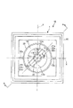
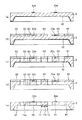
図1は、本発明の光スキャナーの第1実施形態を示す平面図、図2は、図1のA−A線断面図、図3は、図1に示す光スキャナーが備える駆動手段の電圧印加手段を示すブロック図、図4は、図3に示す第1の電圧発生部および第2の電圧発生部での発生電圧の一例を示す図である。なお、以下では、説明の便宜上、図1中の紙面手前側を「上」、紙面奥側を「下」、右側を「右」、左側を「左」と言い、図2中の上側を「上」、下側を「下」、右側を「右」、左側を「左」と言う。
Preferred embodiments of a mirror device, a mirror device manufacturing method, an optical scanner, and an image forming apparatus according to the present invention will be described below with reference to the accompanying drawings. In the following embodiment, a case where the mirror device of the present invention is applied to an optical scanner will be described as a representative example.
<First Embodiment>
1 is a plan view showing a first embodiment of the optical scanner of the present invention, FIG. 2 is a cross-sectional view taken along the line AA of FIG. 1, and FIG. 3 is a voltage application of driving means provided in the optical scanner shown in FIG. FIG. 4 is a block diagram showing the means, and FIG. 4 is a diagram showing an example of the voltage generated in the first voltage generator and the second voltage generator shown in FIG. In the following, for convenience of explanation, the front side of the paper in FIG. 1 is called “up”, the back side of the paper is called “down”, the right side is called “right”, the left side is called “left”, and the upper side in FIG. The upper side, the lower side is called “lower”, the right side is called “right”, and the left side is called “left”.
図1および図2に示すように、光スキャナー10は、ミラーデバイス1と、ホルダー17と、コイル30と、コイル30に電圧を印加する電圧印加手段40とを備えている。ミラーデバイス1は、可動板本体110および光反射性を有する光反射部12を備える可動板11と、1対の軸部材(第1の軸部材)13a、13bと、枠状部材14と、1対の軸部材(第2の軸部材)15a、15bと、支持枠16と、永久磁石(磁石)20と、枠状部材14と永久磁石20とを接合し、空間23を形成するための半田層(第1の半田層)21aおよび半田層(第2の半田層)21bと、枠状部材14と半田層21aとの間に介在する下地層(第1の下地層)22aと、枠状部材14と半田層21bとの間に介在する下地層(第2の下地層)22bと、永久磁石20と半田層21aとの間に介在する下地層(第3の下地層)22cと、永久磁石20と半田層21bとの間に介在する下地層(第4の下地層)22dとを備えている。光反射部12は、可動板本体110の上面に設けられている。
As shown in FIGS. 1 and 2, the
可動板11(光反射部12)と、軸部材13a、13bと、枠状部材14と、軸部材15a、15bと、永久磁石20と、半田層21a、21bと、下地層22a、22b、22c、22dとで、軸部材15a、15bを回動軸とする第2の振動系が構成され、可動板11(光反射部12)と、軸部材13a、13bとで、軸部材13a、13bを回動軸とする第1の振動系が構成される。
Movable plate 11 (light reflecting portion 12),
枠状部材14は、軸部材15a、15bによって支持枠16に支持されている。また、可動板11は、枠状部材14の内側に配置され、軸部材13a、13bによって枠状部材14に支持されている。すなわち、枠状部材14は、可動板11を囲んでいる。また、支持枠16は、ホルダー17に支持されている。
可動板11の形状は、図示の構成では、平面視で円形をなしているが、これに限定されず、平面視で、例えば、楕円形、四角形等の多角形であってもよい。また、枠状部材14の形状は、図示の構成では、平面視でその外形形状が円形をなしているが、枠状であれば特に限定されず、平面視で外形形状が、例えば、円形、楕円形、四角形等の多角形であってもよい。
The frame-
The shape of the
軸部材13a、13bおよび軸部材15a、15bは、それぞれ、弾性変形可能である。軸部材15a、15bは、枠状部材14を図1に示すX軸(第2の軸)周りに回動(搖動)可能とするように、枠状部材14と支持枠16を連結している。この場合、軸部材15a、15bは、枠状部材14のX軸に沿う方向の両端に接続され、枠状部材14を支持枠16に両持ち支持する。また、軸部材13a、13bは、可動板11を図1に示すY軸(第1の軸)周りに回動(搖動)可能とするように、可動板11と枠状部材14を連結している。この場合、軸部材13a、13bは、可動板11のY軸に沿う方向の両端に接続され、可動板11を枠状部材14に両持ち支持する。なお、X軸とY軸は、互いに直交している。また、枠状部材14の中心および可動板11の中心は、図1の平面視にて、X軸とY軸の交点上に位置している。なお、軸部材15a、15bの軸線は、X軸と一致し、軸部材13a、13bの軸線は、Y軸と一致している。
The
枠状部材14をX軸周りに回動可能とし、可動板11をY軸周りに回動可能とすることにより、可動板11をX軸およびY軸の直交する2軸周りに回動させることができる。
可動板11、軸部材13a、13b、枠状部材14、軸部材15a、15b、および支持枠16は、例えばシリコンを主材料として一体に形成されている。シリコンを主材料とすることにより、優れた回動特性を実現できるとともに、優れた耐久性を発揮することができる。また、微細な処理(加工)が可能であり、光スキャナー10の小型化を図ることができる。なお、SOI基板等の積層構造を有する基板を用いてこれらを形成してもよく、この場合、可動板11、軸部材13a、13b、枠状部材14、軸部材15a、15b、および支持枠16が一体となるように、積層構造基板の1つの層で形成するのが好ましい。
By making the frame-
The
ホルダー17は、例えば、ガラスやシリコンを主材料として構成されている。ホルダー17の形状は、図示の構成では、凹状をなし、また、平面視で四角形をなしているが、支持枠16を支持することができれば特に限定されない。支持枠16とホルダー17との接合方法は、特に限定されず、例えば接着剤を用いて接合してもよいし、陽極接合により接合してもよい。また、例えば、支持枠16とホルダー17との間にSiO2を主材料として構成されたSiO2層が介在していてもよい。
The
枠状部材14の下面(ホルダー17と対向する面)には、永久磁石20が設けられている。この永久磁石20は、永久磁石20と可動板11との干渉(接触)を防止する空間23を形成するスペーサーの機能を有する半田層21a、21bにより、下地層22a、22b、22c、22dを介して枠状部材14に接合されている。すなわち、半田層21aにより永久磁石20の長手方向の一方の端部が枠状部材14に接合され、半田層20bにより永久磁石20の長手方向の他方の端部が枠状部材14に接合されている。そして、枠状部材14と半田層21aとの間に下地層22aが介在し、枠状部材14端部と半田層21bとの間に下地層22bが介在し、永久磁石20の一方端部と半田層21aとの間に下地層22cが介在し、永久磁石20の他方の端部と半田層21bとの間に下地層22dが介在している。
A
また、ホルダー17の上面には、永久磁石20に作用する磁界を発生するコイル30が設けられている。コイル30は電圧印加手段40に電気的に接続されている。永久磁石20、コイル30および電圧印加手段40によって可動板11および枠状部材14を回動させる駆動手段が構成される。
永久磁石20は、長手形状、図示の構成では、板状でかつ真っ直ぐな棒状をなしており、その長手方向に磁化されている。すなわち、永久磁石20のS極とN極とを結ぶ線分の方向が、永久磁石20の長手方向と一致している。換言すれば、永久磁石20のS極とN極とを結ぶ線分が、永久磁石20の軸線と一致している。なお、永久磁石20の形状は、長手形状であれば、特に限定されるものではない。
A
The
永久磁石20は、その両極がX軸およびY軸をそれぞれ挟んで配置されている。換言すれば、永久磁石20は、両端部(各磁極)が、X軸で分割される2つの領域に位置し、かつY軸で分割される2つの領域に位置するように配置されている。すなわち、永久磁石20は、図1の平面視にて、その中心が可動板11の中心と一致し、その軸線がX軸およびY軸のそれぞれに対して傾斜するように配置されている。
The
X軸、すなわち軸部材15a、15bの軸線と、永久磁石20の軸線とのなす角(X軸に対する永久磁石20の軸線の傾斜角)θは、特に限定されないが、30°以上60°以下であるのが好ましく、40°以上50°以下度であることがより好ましく、45度であるのがさらに好ましい。このように永久磁石20を設けることで、円滑かつ確実に可動板11をX軸の周りおよびY軸の周りに回動させることができる。これに対し、傾斜角θが前記下限値未満であると、電圧印加手段40によりコイル30に印加される電圧の強さなどの諸条件によっては、円滑に可動板11をX軸周りに回動させることができない場合がある。一方、傾斜角θが前記上限値を超えると、電圧印加手段40によりコイル30に印加される電圧の強さなどの諸条件によっては、円滑に可動板11をY軸周りに回動させることができない場合がある。
The angle θ between the X axis, that is, the axis of the
永久磁石20としては、例えば、ネオジム磁石、フェライト磁石、サマリウムコバルト磁石、アルニコ磁石、ボンド磁石などの硬磁性体を着磁したものを好適に用いることができる。
なお、光スキャナー10を製造する際は、既に着磁がなされて永久磁石20となったもの枠状部材14に設置してもよいし、また、着磁前の硬磁性体を枠状部材14に設置してから、その硬磁性体を着磁することで永久磁石20としてもよい。
As
When the
半田層21a、21bは、それぞれ、半田で構成されている。用いる半田としては、特に限定されず、例えば、Sn−Pb系、Sn−Pb−Bi系、Sn−Pb−Ag系、Sn−Sb系、Sn−Cu系、Sn−Pb−Sb系、Sn−Pb−Cu系、Sn−Ag系、Sn−Ag−Cu系、Sn−Ag−Bi−Cu系、Sn−In−Ag−Bi系、Sn−Zn系、Sn−Zn−Bi系、Sn−Bi系、Sn−In系、Pb−Ag系、Au系等が挙げられる。 The solder layers 21a and 21b are each made of solder. The solder to be used is not particularly limited. For example, Sn—Pb, Sn—Pb—Bi, Sn—Pb—Ag, Sn—Sb, Sn—Cu, Sn—Pb—Sb, Sn— Pb-Cu, Sn-Ag, Sn-Ag-Cu, Sn-Ag-Bi-Cu, Sn-In-Ag-Bi, Sn-Zn, Sn-Zn-Bi, Sn-Bi System, Sn-In system, Pb-Ag system, Au system and the like.
なお、半田層21a、21bには、それぞれ、半田以外の材料、例えば、フラックス機能(活性)を有する化合物等が含まれていてもよい。
永久磁石20は、半田層21a、21bにより、下地層22a、22b、22c、22dを介して枠状部材14に接合されている。これにより、枠状部材14と永久磁石20とを強固に接合することができ、高温多湿の環境下においても永久磁石20が枠状部材14から剥離してしまうことを防止することができる。
The solder layers 21a and 21b may each contain a material other than solder, for example, a compound having a flux function (activity).
The
また、半田層21a、21bは、永久磁石20と可動板11との干渉(接触)を防止する空間23を形成するスペーサーの機能を有している。これにより、ミラーデバイス1の製造において、別途スペーサーを形成する工程が不要となり、ミラーデバイス1の製造にかかる手間を低減することができ、ミラーデバイス1の製造の簡易化を図ることができる。また、このような空間23を形成することで、可動板11のY軸周りの回動を極めて円滑に行うことができる。
In addition, the solder layers 21 a and 21 b have a function of a spacer that forms a
なお、半田層21a、下地層22aおよび22cと、半田層21b、下地層22bおよび22dとにより、それぞれ、スペーサーが構成される。
下地層22a、22bは、それぞれ、枠状部材14の下面(ホルダー17と対向する面)に設けられるものであり、その表面の半田の濡れ性が枠状部材14よりも高くなるように構成されている。これにより半田層21a、21bにより永久磁石20を接合する際、下地層22a、22b上に半田が確実に、かつ均一に濡れ広がることができる。
The
The
また、下地層22c、22dは、それぞれ、永久磁石20の長手方向の一方の端部上と、他方の端部上とに設けられるものであり、その表面の半田の濡れ性が永久磁石20よりも高くなるように構成されている。これにより半田層21a、21bにより永久磁石20を接合する際、下地層22a、22b上に半田が確実に、かつ均一に濡れ広がることができる。
The
したがって、枠状部材14と半田層21a、21bとの間に下地層22a、22bを介在させ、永久磁石20と半田層21a、21bとの間に下地層22c、22dを介在させることにより、それらの下地層22a、22b、22c、22dを介して枠状部材14と永久磁石とを確実に接合することができる。
また、本実施形態では、図1の平面視で、下地層22aと下地層22bとの面積は、等しく設定されている。そして、半田層21aと半田層21bとの体積は、等しく設定さている。半田層21a、21bにより永久磁石20を接合する際は、半田は、下地層22a、22bの表面全体に濡れ広がるので、これにより、半田層21aと半田層21bとの高さが等しくなり、永久磁石20の一方の端部の枠状部材14からの離間距離と、他方の端部の枠状部材14からの離間距離とを等しくすることができる。これによって、可動板11を円滑にX軸周りおよびY軸周りに回動させることができる。
Accordingly, the base layers 22a and 22b are interposed between the frame-shaped
In the present embodiment, the areas of the
また、本実施形態では、図1の平面視で、下地層22cと下地層22dとの面積は、等しく設定されている。
なお、図1の平面視で、下地層22aと下地層22bとの面積は、異なっていてもよく、また、下地層22cと下地層22dとの面積は、異なっていてもよく、また、半田層21aと半田層21bとの体積は、異なっていてもよい。
In the present embodiment, the areas of the
In the plan view of FIG. 1, the areas of the
下地層22a、22bの構成材料としては、それぞれ、その下地層22a、22bの表面の半田の濡れ性が枠状部材14よりも高いものであれば、特に限定されないが、例えば、各種金属材料を用いることが好ましい。下地層22a、22bを金属で構成することにより、下地層22a、22bの半田の濡れ性を向上させることができる。なお、前記金属には、合金等も含まれる。
The constituent material of the base layers 22a and 22b is not particularly limited as long as the wettability of the solder on the surface of the base layers 22a and 22b is higher than that of the
また、下地層22c、22dの構成材料としては、それぞれ、その下地層22c、22dの表面の半田の濡れ性が永久磁石20よりも高いものであれば、特に限定されないが、例えば、各種金属材料を用いることが好ましい。下地層22c、22dを金属で構成することにより、下地層22c、22dの半田の濡れ性を向上させることができる。なお、前記金属には、合金等も含まれる。
The constituent materials of the base layers 22c and 22d are not particularly limited as long as the solder wettability of the surfaces of the base layers 22c and 22d is higher than that of the
また、下地層22a、22b、22c、22dは、それぞれ、単層であってもよく、また、複数の層が積層されたものであってもよい。
下地層22a、22b、22c、22dを3層で構成する場合の具体例としては、それぞれ、例えば、Crで構成されたCr層(第1層)と、Niで構成されたNi層(第2層)と、Auで構成されたAu層(第3層)とをこの順序で積層したもの等が挙げられる。各下地層22a、22b、22c、22dは、それぞれ、Au層が半田層21a、21b側に位置するように形成される。
In addition, each of the base layers 22a, 22b, 22c, and 22d may be a single layer or may be a stack of a plurality of layers.
As specific examples of the case where the
ここで、Cr層は、Ni層と枠状部材14または永久磁石20との密着性を良くするものである。また、Ni層は、Cr層とAu層との密着を保持しつつ、半田を溶融して半田層21、22bを形成する際、その半田の構成材料の枠状部材14への拡散を防止するものである。また、Au層は、半田の濡れ性を向上し、半田層21、22bとの密着性を良くするとともに、Ni層およびCr層の酸化を防止するものである。
Here, the Cr layer improves the adhesion between the Ni layer and the frame-
なお、Cr層に代えて、例えば、Ni−Cr系合金、Ti、Ta等で構成された層を用いることができる。
また、Ni層に代えて、例えば、Ni−Cr系合金、Cr、Ti、Ta等で構成された層を用いることができる。
また、Au層に代えて、例えば、Pd等で構成された層を用いることができる。
In place of the Cr layer, for example, a layer made of Ni—Cr alloy, Ti, Ta, or the like can be used.
Further, instead of the Ni layer, for example, a layer made of Ni—Cr alloy, Cr, Ti, Ta or the like can be used.
Further, for example, a layer made of Pd or the like can be used instead of the Au layer.
また、下地層22a、22b、22c、22dを2層で構成する場合の具体例としては、それぞれ、例えば、Crで構成されたCr層(第1層)と、Auで構成されたAu層(第2層)とをAu層が半田層21a、21b側に位置するように積層したもの、Crで構成されたCr層(第1層)と、Niで構成されたNi層(第2層)とをNi層が半田層21a、21b側に位置するように積層したもの、Niで構成されたNi層(第1層)と、Auで構成されたAu層(第2層)とをAu層が半田層21a、21b側に位置するように積層したもの、Tiで構成されたTi層(第1層)と、Auで構成されたAu層(第2層)とをAu層が半田層21a、21b側に位置するように積層したもの、Wで構成されたW層(第1層)と、Auで構成されたAu層(第2層)とをAu層が半田層21a、21b側に位置するように積層したもの等が挙げられる。
In addition, specific examples of the case where the
永久磁石20の直下には、コイル30が設けられている。すなわち、可動板11および枠状部材14の下面に対向するように、コイル30が設けられている。これにより、コイル30から発生する磁界を効率的に永久磁石20に作用させることができる。これにより、光スキャナー10の省電力化および小型化を図ることができる。
コイル30は、電圧印加手段40と電気的に接続されている。そして、電圧印加手段40によりコイル30に電圧が印加されることで、コイル30からX軸およびY軸に直交する磁束を有する磁界が発生する。なお、コイル30は磁心に巻き付けられていてもよい。
A
The
電圧印加手段40は、図3に示すように、可動板11をX軸周りに回動させるための第1の電圧V1を発生させる第1の電圧発生部41と、可動板11をY軸周りに回動させるための第2の電圧V2を発生させる第2の電圧発生部42と、第1の電圧V1と第2の電圧V2とを重畳し、その電圧をコイル30に印加する電圧重畳部43とを備えている。
第1の電圧発生部41は、図4(a)に示すように、周期T1で周期的に変化する第1の電圧V1(垂直走査用電圧)を発生させるものである。
As shown in FIG. 3, the
As shown in FIG. 4A, the
第1の電圧V1は、鋸波のような波形をなしている。そのため、光スキャナー10は効果的に光を垂直走査(副走査)することができる。なお、第1の電圧V1の波形は、これに限定されない。ここで、第1の電圧V1の周波数(1/T1)は、垂直走査に適した周波数であれば、特に限定されないが、30〜80Hz(60Hz程度)であるのが好ましい。
The first voltage V1 has a waveform like a sawtooth wave. Therefore, the
本実施形態では、第1の電圧V1の周波数は、可動板11と、軸部材13a、13bと、枠状部材14と、軸部材15a、15bと、永久磁石20と、半田層21a、21bと、下地層22a、22b、22c、22dとで構成された第2の振動系のねじり共振周波数(共振周波数)と異なる周波数となるように調整されている。
一方、第2の電圧発生部42は、図4(b)に示すように、周期T1と異なる周期T2で周期的に変化する第2の電圧V2(水平走査用電圧)を発生させるものである。
In the present embodiment, the frequency of the first voltage V1 includes the
On the other hand, as shown in FIG. 4B, the second voltage generator 42 generates a second voltage V2 (horizontal scanning voltage) that periodically changes at a period T2 different from the period T1. .
第2の電圧V2は、正弦波のような波形をなしている。そのため、光スキャナー10は効果的に光を主走査することができる。なお、第2の電圧V2の波形は、これに限定されない。
このような第2の電圧V2の周波数(第2周波数)は、第1の電圧V1の周波数(第1周波数)よりも大きいことが好ましい。すなわち、周期T2は、周期T1よりも短いことが好ましい。これにより、より確実かつより円滑に、可動板11をX軸周りに第1周波数で回動させつつ、Y軸周りに第2周波数で回動させることができる。
The second voltage V2 has a waveform like a sine wave. Therefore, the
The frequency of the second voltage V2 (second frequency) is preferably larger than the frequency of the first voltage V1 (first frequency). That is, the period T2 is preferably shorter than the period T1. Thereby, it is possible to rotate the
また、第2周波数は、第1周波数と異なり、かつ、水平走査に適した周波数であれば、特に限定されないが、10〜40kHzであるのが好ましい。このように、第2の電圧V2の周波数を10〜40kHzとし、前述したように第1の電圧V1の周波数を60Hz程度とすることで、ディスプレイでの描画に適した周波数で、可動板11を互いに直交する2軸(X軸およびY軸)のそれぞれの軸周りに回動させることができる。ただし、可動板11をX軸およびY軸のそれぞれの軸周りに回動させることができれば、第1の電圧V1の周波数と第2の電圧V2の周波数との組み合わせは、特に限定されない。
The second frequency is not particularly limited as long as it is different from the first frequency and is suitable for horizontal scanning, but is preferably 10 to 40 kHz. As described above, the frequency of the second voltage V2 is set to 10 to 40 kHz, and the frequency of the first voltage V1 is set to about 60 Hz as described above, so that the
本実施形態では、第2周波数は、可動板11と、軸部材13a、13bとで構成される軸部材13a、13bを回動軸とする第1の振動系のねじり共振周波数(f2)と等しくなるように設定されている。つまり、第1の振動系は、そのねじり共振周波数f2が水平走査に適した周波数になるように設計(製造)されている。これにより、可動板11のY軸周りの回動角を大きくすることができる。また、第1周波数は、可動板11と、軸部材13a、13bと、枠状部材14と、軸部材15a、15bと、永久磁石20と、半田層21a、21bと、下地層22a、22b、22c、22dとで構成される軸部材15a、15bを回動軸とする第2の振動系のねじり共振周波数(f1)の10分の1以下であることが望ましい。第2の振動系を非共振状態(振幅ゲインが1)で駆動するためには、第1周波数はf1の10分の1以下に設定する必要がある。10分の1より大きい周波数で駆動すると、第2の振動系の共振を起こす可能性があるからである。
In the present embodiment, the second frequency is equal to the torsional resonance frequency (f2) of the first vibration system using the
また、第2周波数は、第2の振動系を非共振状態(振幅ゲインが1)で駆動するため、第1周波数の10倍以上に設定することが望ましい。第2周波数が第1周波数に対して10倍未満であると、第2の電圧V2をコイル30に印加した時に、第2の振動系も回転運動してしまい、駆動信号のクロストークが発生してしまう。なお、上述のように、第1周波数はf1の10分の1以下が望ましいので、これらの関係から第2周波数は第1周波数よりも大きいことが望ましい。
The second frequency is preferably set to 10 times or more of the first frequency in order to drive the second vibration system in a non-resonant state (amplitude gain is 1). If the second frequency is less than 10 times the first frequency, when the second voltage V2 is applied to the
また、第2の振動系のねじり共振周波数をf1[Hz]とし、第1の振動系のねじり共振周波数をf2[Hz]としたとき、f1とf2とが、f2>f1の関係を満たすことが好ましく、f2≧10f1の関係を満たすことがより好ましい。これにより、より円滑に、可動板11をX軸周りに第1の電圧V1の周波数で回動させつつ、Y軸周りに第2の電圧V2の周波数で回動させることができる。f2≦f1とした場合は、第1周波数による第1の振動系の振動が起こる可能性がある。
Further, when the torsional resonance frequency of the second vibration system is f1 [Hz] and the torsional resonance frequency of the first vibration system is f2 [Hz], f1 and f2 satisfy the relationship of f2> f1. Is preferable, and it is more preferable to satisfy the relationship of f2 ≧ 10f1. As a result, the
このような第1の電圧発生部41および第2の電圧発生部42は、それぞれ、制御部70に接続され、この制御部70からの信号に基づき駆動する。このような第1の電圧発生部41および第2の電圧発生部42には、電圧重畳部43が接続されている。
電圧重畳部43は、コイル30に電圧を印加するための加算器43aを備えている。加算器43aは、第1の電圧発生部41から第1の電圧V1を受けるとともに、第2の電圧発生部42から第2の電圧V2を受け、これらの電圧を重畳しコイル30に印加するようになっている。
The first
The
次に、光スキャナー10の駆動方法について説明する。なお、本実施形態では、前述したように、第1の電圧V1の周波数は、第2の振動系のねじり共振周波数と異なる値に設定されており、第2の電圧V2の周波数は、第1の振動系のねじり共振周波数と等しく、かつ、第1の電圧V1の周波数よりも大きくなるように設定されている(例えば、第1の電圧V1の周波数が60Hzで、第2の電圧V2の周波数が15kHz)。
Next, a method for driving the
例えば、図4(a)に示すような第1の電圧V1と、図4(b)に示すような第2の電圧V2とを電圧重畳部43にて重畳し、重畳した電圧をコイル30に印加する。
すると、第1の電圧V1によって、枠状部材14と永久磁石20のN極との接合部付近をコイル30に引き付けようとするとともに、枠状部材14と永久磁石20のS極との接合部付近をコイル30から離間させようとする磁界(この磁界を「磁界A1」という)と、枠状部材14と永久磁石20のN極との接合部付近をコイル30から離間させようとするとともに、枠状部材14と永久磁石20のS極との接合部付近をコイル30に引き付けようとする磁界(この磁界を「磁界A2」という)とが交互に切り換わる。
For example, the
Then, the first voltage V <b> 1 tries to attract the vicinity of the joint between the frame-shaped
ここで、上述したように、永久磁石20は、それぞれの端部(磁極)が、X軸で分割される2つの領域に位置するように配置される。すなわち図1の平面視において、X軸を挟んで一方側に永久磁石20のN極が位置し、他方側にS極が位置している。そのため、磁界A1と磁界A2とが交互に切り換わることで、軸部材15a、15bを捩れ変形させつつ、枠状部材14が可動板11とともに、第1の電圧V1の周波数でX軸周りに回動する。
Here, as described above, the
なお、第1の電圧V1の周波数は、第2の電圧V2の周波数に比べて極めて低く設定されている。また、第2の振動系のねじり共振周波数は、第1の振動系のねじり共振周波数よりも低く設計されている(例えば、第1の振動系のねじり共振周波数の1/10以下)。つまり、第2の振動系は、第1の振動系よりも振動しやすいように設計されているため、枠状部材14は第1の電圧V1によってX軸周りに回動する。すなわち、第2の電圧V2によって、枠状部材14がX軸周りに回動してしまうことを防止することができる。
Note that the frequency of the first voltage V1 is set to be extremely lower than the frequency of the second voltage V2. The torsional resonance frequency of the second vibration system is designed to be lower than the torsional resonance frequency of the first vibration system (for example, 1/10 or less of the torsional resonance frequency of the first vibration system). That is, since the second vibration system is designed to vibrate more easily than the first vibration system, the frame-
一方、第2の電圧V2によって、枠状部材14と永久磁石20のN極との接合部付近をコイル30に引き付けようとするとともに、枠状部材14と永久磁石20のS極との接合部付近をコイル30から離間させようとする磁界(この磁界を「磁界B1」という)と、枠状部材14と永久磁石20のN極との接合部付近をコイル30から離間させようとするとともに、枠状部材14と永久磁石20のS極との接合部付近をコイル30に引き付けようとする磁界(この磁界を「磁界B2」という)とが交互に切り換わる。
On the other hand, the second voltage V2 tries to attract the vicinity of the joint between the
ここで、上述したように、永久磁石20は、それぞれの端部(磁極)が、Y軸で分割される2つの領域に位置するように配置される。すなわち図1の平面視において、Y軸を挟んで一方側に永久磁石20のN極が位置し、他方側にS極が位置している。そのため、磁界B1と磁界B2とが交互に切り換わることで、軸部材13a、13bを捩れ変形させつつ、可動板11が第2の電圧V2の周波数でY軸まわりに回動する。
なお、第2の電圧V2の周波数は、第1の振動系のねじり共振周波数と等しい。そのため、第2の電圧V2によって可動板11をY軸まわりに回動させることができる。つまり、第1の電圧V1によって、可動板11がY軸まわりに回動してしまうことを防止することができる。
Here, as described above, the
The frequency of the second voltage V2 is equal to the torsional resonance frequency of the first vibration system. Therefore, the
次に、ミラーデバイス1の製造方法の一例について説明する。
<第1の製造方法>
図5は、図1に示す光スキャナーのミラーデバイスを示す平面図、図6〜図8は、図1に示す光スキャナーのミラーデバイスの第1の製造方法を説明するための断面図である。この場合、図6〜図8は、図5のB−B線断面図に対応するものである。なお、以下では、説明の便宜上、図5中の紙面手前側を「上」、紙面奥側を「下」、右側を「右」、左側を「左」と言う。また、図6〜図8では、図2に対して上下が逆になっているが、図6〜図8中の上側を「上」、下側を「下」、右側を「右」、左側を「左」と言う。
Next, an example of a manufacturing method of the
<First manufacturing method>
5 is a plan view showing a mirror device of the optical scanner shown in FIG. 1, and FIGS. 6 to 8 are sectional views for explaining a first manufacturing method of the mirror device of the optical scanner shown in FIG. In this case, FIGS. 6 to 8 correspond to the sectional view taken along the line BB of FIG. In the following, for convenience of explanation, the front side of the sheet in FIG. 5 is referred to as “upper”, the rear side of the sheet is referred to as “lower”, the right side is referred to as “right”, and the left side is referred to as “left”. 6 to 8 are upside down with respect to FIG. 2, but the upper side in FIGS. 6 to 8 is “upper”, the lower side is “lower”, the right side is “right”, and the left side. Is called “left”.
まず、シリコンで構成された基板(シリコン基板)5を用意する。
次に、図6(a)に示すように、基板5を熱酸化し、その基板5の表面に酸化膜51を形成する。そして、基板5の下面側の酸化膜51の形状を、ミラーデバイス1の図2中の上面側の平面視形状に対応する形状にする。
次に、図6(b)に示すように、酸化膜51をマスクとして、基板5を下面側からエッチングする。
First, a substrate (silicon substrate) 5 made of silicon is prepared.
Next, as shown in FIG. 6A, the
Next, as shown in FIG. 6B, the
エッチング方法としては、例えば、プラズマエッチング、リアクティブイオンエッチング、ビームエッチング、光アシストエッチング等の物理的エッチング法、ウェットエッチング等の化学的エッチング法等のうちの1種または2種以上を組み合わせて用いることができる。以下の各工程、後述する第2の製造方法におけるエッチングにおいても、それぞれ、同様の方法を用いることができる。なお、以下のエッチング、、後述する第2の製造方法におけるエッチングでは、それぞれ、その一例を述べる。
前記酸化膜51をマスクとして行う基板5のエッチングにおいては、例えば、エッチング液として水酸化テトラメチルアンモニウム等を用いて、ウェットエッチングを行う。
As an etching method, for example, one or more of physical etching methods such as plasma etching, reactive ion etching, beam etching, and light-assisted etching, and chemical etching methods such as wet etching are used in combination. be able to. The same method can be used for each of the following steps and etching in the second manufacturing method described later. An example of each of the following etching and etching in the second manufacturing method described later will be described.
In the etching of the
次に、図6(c)に示すように、酸化膜51を除去する。この場合、例えば、フッ酸等を用いることができる。そして、基板5を熱酸化し、その基板5の表面に酸化膜52を形成する。
次に、図6(d)に示すように、基板5の上面側の酸化膜52をエッチングして除去する。このエッチングにおいては、例えば、反応性イオンエッチングを行う。
Next, as shown in FIG. 6C, the
Next, as shown in FIG. 6D, the
次に、図6(e)に示すように、基板5の上面に、基板5の上面の下地層22a、22bを形成する部位以外を覆うように、レジスト膜61を形成する。下地層22a、22bを形成する部位の位置は、後述する溶融した半田64a、64bにより永久磁石20の位置決めがなされる際、永久磁石20が適切な位置に位置するように設定される。そして、基板5の上面に、下地層22a、22bとなる部位を含む層62を形成する。なお、層62の構成材料は、下地層22a、22bの構成材料と同一のものである。
Next, as illustrated in FIG. 6E, a resist
次に、図7(a)に示すように、レジスト膜61を除去する。これにより、基板5の上面の所定の位置に、下地層22a、22bが形成される。
次に、図7(b)に示すように、基板5の上面および下地層22a、22bの上面に、可動板本体110(可動板11)と、軸部材13a、13bと、枠状部材14と、軸部材15a、15bと、支持枠16との平面視形状に対応する形状をなすレジスト膜63を形成する。
Next, as shown in FIG. 7A, the resist
Next, as shown in FIG. 7B, on the upper surface of the
次に、図7(c)に示すように、レジスト膜63をマスクとして、基板5を上面側からエッチングする。このエッチングにおいては、例えば、誘導結合型反応性イオンエッチングを行う。
次に、図7(d)に示すように、酸化膜51を除去する。この場合、例えば、フッ酸等を用いることができる。
Next, as shown in FIG. 7C, the
Next, as shown in FIG. 7D, the
次に、図7(e)に示すように、レジスト膜63を除去する。これにより、可動板本体110と、軸部材13a、13bと、下地層22a、22bが設けられた枠状部材14と、軸部材15a、15bと、支持枠16とを備えた基板5が得られる。そして、可動板本体110の下面に、光反射部12を形成する。これにより、光反射部12を有する可動板11と、軸部材13a、13bと、下地層22a、22bが設けられた枠状部材14と、軸部材15a、15bと、支持枠16とを備えた基板5が得られる。
Next, as shown in FIG. 7E, the resist
次に、図8(a)に示すように、下地層22a、22b上に、フラックス機能を有する化合物を塗布して、図示しないフラックス膜を形成し、さらに、各フラックス膜上にそれぞれ図示しない半田ボールを配置し、その半田ボールを溶融する。これにより、半田64a、64bが、それぞれ下地層22a、22b上全体に濡れ広がる。
ここで、下地層22a上に配置する半田ボールの数でその下地層22a上形成される半田層21aの高さを調整し、下地層22b上に配置する半田ボールの数でその下地層22b上形成される半田層21bの高さを調整する。これにより、半田層21a、21bの高さをそれぞれ確実に調整することができる。
Next, as shown in FIG. 8 (a), a compound having a flux function is applied on the
Here, the height of the
次に、図8(b)に示すように、永久磁石20の長手方向の両端部に、下地層22c、22dを形成する。この下地層22c、22dの形成は、例えば、所定のマスクを用いて行うことができる。そして、下地層22c、22d上に、それぞれ、フラックス機能を有する化合物を塗布して、フラックス膜65a、65bを形成する。
次に、図8(c)に示すように、枠状部材14の下地層22a上の半田64aと、永久磁石20側の下地層22c上のフラックス膜65aとが一致し、下地層22b上の半田64bと下地層22d上のフラックス膜65bとが一致するように、永久磁石20を枠状部材14上に載置する。
Next, as shown in FIG. 8B, base layers 22 c and 22 d are formed at both ends in the longitudinal direction of the
Next, as shown in FIG. 8C, the
次に、図8(d)に示すように、半田64a、64bを溶融し、半田層21a、21bを形成し、半田層21aにより、下地層22a、22cを介して枠状部材14と永久磁石20の一方の端部とを接合するとともに、半田層21bにより、下地層22b、22dを介して枠状部材14と永久磁石20の他方の端部とを接合する。枠状部材14と永久磁石20との間には、半田層21a、21b、下地層22a、22b、22c、22dが介在することとなり、空間23が形成される。以上のようにして、ミラーデバイス1が製造される。
Next, as shown in FIG. 8 (d), the
なお、半田64a、64bを溶融した際は、その半田64a、64bにより、永久磁石20が適切な位置に自動的に移動し、その永久磁石20の位置決めがなされる。これによって、永久磁石20を適切な位置に容易かつ確実に位置決めすることができる。
また、下地層22a、22b上にフラックス膜を設け、下地層22c、22d上にフラックス膜65a、65bを設けることにより、半田ボールを溶融して半田層21a、21bを形成する際、半田層21a、21bの表面の酸化膜を除去したり、酸化を防止することができる。
When the
Further, by providing flux films on the base layers 22a and 22b and providing
<第2の製造方法>
図9〜図11は、図1に示すミラーデバイスの第2の製造方法を説明するための断面図である。この場合、図9〜図11は、図5のB−B線断面図に対応するものである。なお、図9〜図11では、図2に対して上下が逆になっているが、以下では、説明の便宜上、図9〜図11中の上側を「上」、下側を「下」、右側を「右」、左側を「左」と言う。また、支持枠16の構造は、前述した第1の製造方法の場合と若干異なっている。
<Second production method>
9 to 11 are cross-sectional views for explaining a second manufacturing method of the mirror device shown in FIG. In this case, FIGS. 9 to 11 correspond to the cross-sectional view taken along the line BB of FIG. 9 to 11 are upside down with respect to FIG. 2, but for the sake of convenience, the upper side in FIGS. 9 to 11 is “upper”, the lower side is “lower”, and The right side is called “right” and the left side is called “left”. Further, the structure of the
以下、第2の製造方法について、前述した第1の製造方法との相違点を中心に説明し、同様の事項については、その説明を省略する。
まず、SOI基板7を用意する。SOI基板7は、Si層(第1のSi層)7a、SiO2層7bおよびSi層(第2のSi層)7cが、図9(a)中上側から下側へ、この順にて積層してなる積層構造基板である。
Hereinafter, the second manufacturing method will be described focusing on the differences from the first manufacturing method described above, and description of similar matters will be omitted.
First, an SOI substrate 7 is prepared. In the SOI substrate 7, a Si layer (first Si layer) 7a, a SiO 2 layer 7b, and a Si layer (second Si layer) 7c are laminated in this order from the upper side to the lower side in FIG. A laminated structure substrate.
次に、図9(a)に示すように、SOI基板7を熱酸化し、そのSOI基板7の表面に酸化膜71を形成する。
次に、図9(b)に示すように、SOI基板7の上面側の酸化膜71をエッチングして除去する。このエッチングにおいては、例えば、反応性イオンエッチングを行う。
次に、図9(c)に示すように、SOI基板7のSi層7aの上面に、Si層7aの上面の下地層22a、22bを形成する部位以外を覆うように、レジスト膜81を形成する。下地層22a、22bを形成する部位の位置は、後述する溶融した半田64a、64bにより永久磁石20の位置決めがなされる際、永久磁石20が適切な位置に位置するように設定される。そして、Si層7aの上面に、下地層22a、22bとなる部位を含む層82を形成する。なお、層82の構成材料は、下地層22a、22bの構成材料と同一のものである。
Next, as shown in FIG. 9A, the SOI substrate 7 is thermally oxidized, and an
Next, as shown in FIG. 9B, the
Next, as shown in FIG. 9C, a resist
次に、図9(d)に示すように、レジスト膜81を除去する。これにより、Si層7aの上面の所定の位置に、下地層22a、22bが形成される。
次に、図9(e)に示すように、Si層7cの下面側の酸化膜71の形状を、ミラーデバイス1の図2中の上面側の平面視形状に対応する形状にする。なお、前述したように、この第2の製造方法で製造されるミラーデバイス1の図2中の上面側の形状は、その図2に示すミラーデバイス1とは若干異なっている。
Next, as shown in FIG. 9D, the resist
Next, as shown in FIG. 9E, the shape of the
次に、図10(a)に示すように、Si層7aの上面および下地層22a、22bの上面に、可動板本体110(可動板11)と、軸部材13a、13bと、枠状部材14と、軸部材15a、15bと、支持枠16との平面視形状に対応する形状をなすレジスト膜83を形成する。
次に、図10(b)に示すように、レジスト膜83をマスクとして、Si層7aを上面側からエッチングする。このエッチングにおいては、例えば、誘導結合型反応性イオンエッチングを行う。このとき、SiO2層7bは、エッチングのストップ層として機能する。
Next, as shown in FIG. 10A, on the upper surface of the
Next, as shown in FIG. 10B, the
次に、図10(c)に示すように、レジスト膜83をマスクとして、Si層7cを下面側からエッチングする。このエッチングにおいては、例えば、誘導結合型反応性イオンエッチングを行う。このとき、SiO2層7bは、エッチングのストップ層として機能する。
次に、図10(d)に示すように、Si層7cの下面側の酸化膜71と、露出しているSiO2層7bとをエッチングして除去する。このエッチングにおいては、例えば、反応性イオンエッチングを行う。
Next, as shown in FIG. 10C, the
Next, as shown in FIG. 10D, the
次に、図10(e)に示すように、レジスト膜83を除去する。これにより、可動板本体110と、軸部材13a、13bと、下地層22a、22bが設けられた枠状部材14と、軸部材15a、15bと、支持枠16とを備えたSOI基板7が得られる。そして、可動板本体110の下面に、光反射部12を形成する。これにより、光反射部12を有する可動板11と、軸部材13a、13bと、下地層22a、22bが設けられた枠状部材14と、軸部材15a、15bと、支持枠16とを備えたSOI基板7が得られる。
Next, as shown in FIG. 10E, the resist
次に、図11(a)に示すように、下地層22a、22b上に、フラックス機能を有する化合物を塗布して、図示しないフラックス膜を形成し、さらに、各フラックス膜上にそれぞれ図示しない半田ボールを配置し、その半田ボールを溶融する。これにより、半田64a、64bが、それぞれ下地層22a、22b上全体に濡れ広がる。
次に、図11(b)に示すように、永久磁石20の長手方向の両端部に、下地層22c、22dを形成する。この下地層22c、22dの形成は、例えば、所定のマスクを用いて行うことができる。そして、下地層22c、22d上に、それぞれ、フラックス機能を有する化合物を塗布して、フラックス膜65a、65bを形成する。
Next, as shown in FIG. 11 (a), a compound having a flux function is applied on the base layers 22a and 22b to form a flux film (not shown), and solder (not shown) is further formed on each flux film. Place the ball and melt the solder ball. As a result, the
Next, as shown in FIG. 11B, base layers 22 c and 22 d are formed at both ends in the longitudinal direction of the
次に、図11(c)に示すように、枠状部材14の下地層22a上の半田64aと、永久磁石20側の下地層22c上のフラックス膜65aとが一致し、下地層22b上の半田64bと下地層22d上のフラックス膜65bとが一致するように、永久磁石20を枠状部材14上に載置する。
次に、図11(d)に示すように、半田64a、64bを溶融し、半田層21a、21bを形成し、半田層21aにより、下地層22a、22cを介して枠状部材14と永久磁石20の一方の端部とを接合するとともに、半田層21bにより、下地層22b、22dを介して枠状部材14と永久磁石20の他方の端部とを接合する。枠状部材14と永久磁石20との間には、半田層21a、21b、下地層22a、22b、22c、22dが介在することとなり、空間23が形成される。以上のようにして、ミラーデバイス1が製造される。
Next, as shown in FIG. 11C, the
Next, as shown in FIG. 11 (d), the
以上説明したように、本実施形態によれば、第1の電圧V1と第2の電圧V2とを重畳させた電圧をコイル30に印加することで、可動板11をX軸周りに第1の電圧V1の周波数で回動させつつ、Y軸周りに第2の電圧のV2の周波数で回動させることができる。これにより、装置の低コスト化および小型化を図るとともに、可動板11をX軸およびY軸のそれぞれの軸周りに回動させることができる。
As described above, according to the present embodiment, by applying a voltage obtained by superimposing the first voltage V1 and the second voltage V2 to the
特に、駆動源となる永久磁石とコイルのそれぞれの数を少なくすることができるため、簡単かつ小型な構成とすることができる。
また、永久磁石20は、半田層21a、21bにより、下地層22a、22b、22c、22dを介して枠状部材14に接合されているので、枠状部材14と永久磁石20とを強固に接合することができ、高温多湿の環境下においても永久磁石20が枠状部材14から剥離してしまうことを防止することができる。
In particular, since the number of permanent magnets and coils serving as driving sources can be reduced, a simple and compact configuration can be achieved.
Further, since the
また、半田層21a、21bは、空間23を形成するスペーサーの機能を有しているので、ミラーデバイス1の製造において、別途スペーサーを形成する工程が不要となり、ミラーデバイス1の製造にかかる手間を低減することができる。
また、ミラーデバイス1の製造において着磁後または着磁前の永永久磁石20を接合する際は、下地層22a、22b上の溶融された半田により、永久磁石20が適切な位置に自動的に移動し、その永久磁石20の位置決めがなされるので、永久磁石20を適切な位置に容易かつ確実に位置決めすることができる。
In addition, since the solder layers 21a and 21b have a function of a spacer for forming the
Further, when the permanent
また、ミラーデバイス1を製造する際は、基板5の所定の位置に下地層22a、22bをそれぞれ形成した後、基板5を所定の形状に加工し、枠状部材14と、軸部材15a、15bと、可動板11と、軸部材13a、13bとをそれぞれ形成するので、枠状部材14を形成する際に、同時に、枠状部材14における下地層22a、22bの位置決めをそれぞれ行うことができ、これによって、製造工程を削減することができ、また、枠状部材14における下地層22a、22bの位置を正確に設定することができる。
Further, when manufacturing the
また、第1の電圧V1および第2の電圧V2を適宜変更することで、第2の振動系および第1の振動系の構造を変更することなく、所望の振動特性を得ることができる。
また、光スキャナー10は、枠状部材14に永久磁石20を設け、永久磁石20に対向するようにホルダー17上にコイル30を設けている。つまり、第2の振動系および第1の振動系上には発熱体であるコイル30が設けられていない。そのため、通電によってコイル30から発生する熱による振動系の撓みや共振周波数の変化を防止または抑制することができる。その結果、光スキャナー10は、長時間の連続使用であっても所望の振動特性を発揮することができる。
In addition, by appropriately changing the first voltage V1 and the second voltage V2, desired vibration characteristics can be obtained without changing the structures of the second vibration system and the first vibration system.
In the
<第2実施形態>
図12は、本発明の光スキャナーの第2実施形態を示す平面図、図13は、図12のC−C線断面図である。
以下、第2実施形態について、前述した第1実施形態との相違点を中心に説明し、同様の事項については、その説明を省略する。
Second Embodiment
12 is a plan view showing a second embodiment of the optical scanner of the present invention, and FIG. 13 is a cross-sectional view taken along the line CC of FIG.
Hereinafter, the second embodiment will be described with a focus on the differences from the first embodiment described above, and the description of the same matters will be omitted.
図12および図13に示すように、第2実施形態の光スキャナー10では、下地層22aにおける永久磁石20の長手方向の下地層22bと反対側の端部と、下地層22bにおける永久磁石20の長手方向の下地層22aと反対側の端部との間の距離L2は、永久磁石20の長手方向の長さL1よりも長く設定されている。すなわち、下地層22aは、永久磁石20一方の端部から永久磁石20の長手方向に突出し、下地層22bは、永久磁石20の他方の端部から永久磁石20の長手方向に突出している。
As shown in FIGS. 12 and 13, in the
同様に、半田層21aは、永久磁石20一方の端部から永久磁石20の長手方向に突出し、半田層21bは、永久磁石20の他方の端部から永久磁石20の長手方向に突出している。
これにより、着磁後または着磁前の永久磁石20を枠状部材14に接合する際、溶融された半田による永久磁石20の位置決めを確実に行うことができ、また、永久磁石20と枠状部材14とを強固に接合することができる。
Similarly, the
Accordingly, when the
また、下地層22aは、永久磁石20一方の端部から永久磁石20の長手方向に対して直交する方向に突出し、下地層22bは、永久磁石20の他方の端部から永久磁石20の長手方向に対して直交する方向に突出している。
同様に、半田層21aは、永久磁石20一方の端部から永久磁石20の長手方向に対して直交する方向に突出し、半田層21bは、永久磁石20の他方の端部から永久磁石20の長手方向に対して直交する方向に突出している。
The
Similarly, the
これにより、永久磁石20を枠状部材14に接合する際、溶融された半田による永久磁石20の位置決めをより確実に行うことができ、また、永久磁石20と枠状部材14とをより強固に接合することができる。
以上説明したような光スキャナー10は、光反射部12を備えているため、例えば、レーザープリンター、バーコードリーダー、走査型共焦点レーザー顕微鏡や、プロジェクター、ヘッドアップディスプレイ(HUD)、ヘッドマウントディスプレイ(HMD)のようなイメージング用ディスプレイ等の画像形成装置が備える光スキャナーに好適に適用することができる。
Thereby, when joining the
Since the
<画像形成装置の実施形態>
図14は、本発明の画像形成装置の実施形態を模式的に示す図である。
本実施形態では、画像形成装置の一例として、光スキャナー10をイメージング用ディスプレイの光スキャナーとして用いた場合を説明する。なお、スクリーンSの長手方向を「横方向」といい、長手方向に直角な方向を「縦方向」という。また、X軸、すなわち回動中心軸XがスクリーンSの横方向と平行であり、Y軸、すなわち回動中心軸YがスクリーンSの縦方向と平行である。
<Embodiment of Image Forming Apparatus>
FIG. 14 is a diagram schematically showing an embodiment of the image forming apparatus of the present invention.
In this embodiment, a case where the
画像形成装置(プロジェクター)9は、レーザーなどの光を照出する光源装置(光源)91と、複数のダイクロイックミラー92、92、92と、光スキャナー10とを有している。
光源装置91は、赤色光を照出する赤色光源装置911と、青色光を照出する青色光源装置912と、緑色光を照出する緑色光源装置913とを備えている。
The image forming apparatus (projector) 9 includes a light source device (light source) 91 that emits light such as a laser, a plurality of
The light source device 91 includes a red
各ダイクロイックミラー92は、赤色光源装置911、青色光源装置912、緑色光源装置913のそれぞれから照出された光を合成する光学素子である。
このようなプロジェクター9は、図示しないホストコンピューターからの画像情報に基づいて、光源装置91(赤色光源装置911、青色光源装置912、緑色光源装置913)から照出された光をダイクロイックミラー92で合成し、この合成された光が光スキャナー10によって2次元走査され、スクリーンS上でカラー画像を形成するように構成されている。
Each
Such a projector 9 combines light emitted from the light source device 91 (red
2次元走査の際、光スキャナー10の可動板11の、回動中心軸Y回りの回動により光反射部12で反射した光がスクリーンSの横方向に走査(主走査)される。一方、光スキャナー10の可動板11の、回動中心軸X回りの回動により光反射部12で反射した光がスクリーンSの縦方向に走査(副走査)される。
なお、図14中では、ダイクロイックミラー92で合成された光を光スキャナー10によって2次元的に走査した後、その光を固定ミラーKで反射させてからスクリーンSに画像を形成するように構成されているが、固定ミラーKを省略し、光スキャナー10によって2次元的に走査された光を直接スクリーンSに照射してもよい。
During the two-dimensional scanning, the light reflected by the
In FIG. 14, the light synthesized by the
以上、本発明のミラーデバイス、ミラーデバイスの製造方法、光スキャナーおよび画像形成装置を、図示の実施形態に基づいて説明したが、本発明はこれに限定されるものではなく、各部の構成は、同様の機能を有する任意の構成のものに置換することができる。また、本発明に、他の任意の構成物や、工程が付加されていてもよい。
また、本発明は、前記各実施形態のうちの、任意の2以上の構成(特徴)を組み合わせたものであってもよい。
なお、前記実施形態では、磁石として、永久磁石を用いているが、本発明では、磁石として、電磁石を用いてもよい。
また、本発明では、下地層22c、22dは、省略されていてもよい。
As described above, the mirror device, the manufacturing method of the mirror device, the optical scanner, and the image forming apparatus of the present invention have been described based on the illustrated embodiment, but the present invention is not limited to this, and the configuration of each unit is as follows. Any structure having a similar function can be substituted. Moreover, other arbitrary structures and processes may be added to the present invention.
Further, the present invention may be a combination of any two or more configurations (features) of the above embodiments.
In the embodiment, a permanent magnet is used as the magnet. However, in the present invention, an electromagnet may be used as the magnet.
In the present invention, the foundation layers 22c and 22d may be omitted.
1…ミラーデバイス 10…光スキャナー 11…可動板 110…可動板本体 111…凹部 12…光反射部 13a、13b…軸部材 14…枠状部材 15a、15b…軸部材 16…支持枠 17…ホルダー 20…永久磁石 21a、21b…半田層 22a、22b、22c、22d…下地層 23…空間 30…コイル 40…電圧印加手段 41…第1の電圧発生部 42…第2の電圧発生部 43…電圧重畳部 43a…加算器 70…制御部 5…基板 51、52…酸化膜 61、63…レジスト膜 62…層 64a、64b…半田 65a、65b…フラックス膜 7…SOI基板 7a、7c…Si層 7b…SiO2層 71…酸化膜 81、83…レジスト膜 82…層 9…プロジェクター 91…光源装置 911…赤色光源装置 912…青色光源装置 913…緑色光源装置 92…ダイクロイックミラー
DESCRIPTION OF
Claims (10)
前記可動板の前記第1の軸に沿う方向の両端に接続された第1の軸部材と、
前記可動板を囲んでおり、前記第1の軸部材が接続され、前記第1の軸に交差する第2の軸周りに搖動可能な枠状部材と、
前記枠状部材の前記第2の軸に沿う方向の両端に接続された第2の軸部材と、
前記枠状部材に設けられたれた第1の下地層および第2の下地層と、
前記枠状部材に配置され、一方の磁極と他方の磁極とが前記第1の軸および前記第2の軸をそれぞれ挟んで配置された磁石と、
前記可動板と前記磁石との間に、前記第1の下地層および前記第2の下地層と前記磁石との間に介在して前記枠状部材と前記磁石とを接合する半田で構成された第1の半田層および第2の半田層と、を備え、
前記第1の下地層および前記第2の下地層は、前記枠状部材よりも前記半田の濡れ性が高く、
前記磁石は長手形状をなし、
前記第1の半田層により前記磁石の長手方向の一方の端部が接合され、前記第2の半田層により前記磁石の長手方向の他方の端部が接合されており、
前記第1の下地層における前記磁石の長手方向の前記第2の下地層と反対側の端部と、前記第2の下地層における前記磁石の長手方向の前記第1の下地層と反対側の端部との間の距離は、前記磁石の長手方向の長さよりも長いことを特徴とするミラーデバイス。 A movable plate provided with a light reflecting portion having light reflectivity and swingable about a first axis;
A first shaft member connected to both ends of the movable plate in the direction along the first axis;
A frame-shaped member that surrounds the movable plate, is connected to the first shaft member, and is swingable around a second axis that intersects the first axis;
A second shaft member connected to both ends of the frame-shaped member in a direction along the second axis;
A first underlayer and a second underlayer provided on the frame member;
A magnet disposed on the frame-shaped member, wherein one magnetic pole and the other magnetic pole are disposed with the first axis and the second axis interposed therebetween,
Between the movable plate and the magnet, the first base layer, the second base layer, and the magnet are interposed between the magnet and the frame-shaped member and the magnet. A first solder layer and a second solder layer;
Said first underlayer and the second underlayer, wettability of the solder than the frame-like member is rather high,
The magnet has a longitudinal shape,
One end of the magnet in the longitudinal direction is joined by the first solder layer, and the other end in the longitudinal direction of the magnet is joined by the second solder layer,
An end of the first underlayer opposite to the second underlayer in the longitudinal direction of the magnet, and an end of the second underlayer opposite to the first underlayer in the longitudinal direction of the magnet. The distance between the end portions is longer than the length in the longitudinal direction of the magnet .
前記第1の下地層と前記第2の下地層との面積が等しい請求項1に記載のミラーデバイス。 Equal volumes of the previous SL first solder layer and the second solder layer,
Said first base layer and the second base layer and the mirror device area according to have equal claim 1.
前記第1の半田層により前記磁石の長手方向の一方の端部が接合され、前記第2の半田層により前記磁石の長手方向の他方の端部が接合されており、
前記第1の下地層と前記第2の下地層との面積が等しく、
前記第1の下地層は、前記磁石の前記一方の端部から該磁石の長手方向に突出し、前記第2の下地層は、前記磁石の前記他方の端部から該磁石の長手方向に突出している請求項1に記載のミラーデバイス。 The volume of the first solder layer and the second solder layer is equal,
One end of the magnet in the longitudinal direction is joined by the first solder layer, and the other end in the longitudinal direction of the magnet is joined by the second solder layer,
The areas of the first underlayer and the second underlayer are equal,
The first underlayer protrudes from the one end of the magnet in the longitudinal direction of the magnet, and the second underlayer protrudes from the other end of the magnet in the longitudinal direction of the magnet. The mirror device according to claim 1.
前記可動板の前記第1の軸に沿う方向の両端に接続された第1の軸部材と、
前記可動板を囲んでおり、前記第1の軸部材が接続され、前記第1の軸に交差する第2の軸周りに搖動可能な枠状部材と、
前記枠状部材の前記第2の軸に沿う方向の両端に接続された第2の軸部材と、
前記枠状部材に設けられた第1の下地層および第2の下地層と、
前記枠状部材に配置され、一方の磁極と他方の磁極とが前記第1の軸および前記第2の軸をそれぞれ挟んで配置された磁石と、を備えるミラーデバイスの製造方法であって、
前記枠状部材に前記枠状部材よりも半田の濡れ性が高い第1の下地層および第2の下地層をそれぞれ形成する工程と、
基板の所定の位置に前記第1の下地層および前記第2の下地層をそれぞれ形成した後、前記基板を所定の形状に加工し、前記枠状部材と、前記第1の軸部材と、前記可動板と、前記第2の軸部材とをそれぞれ形成する工程と、
前記第1の下地層および前記第2の下地層上にそれぞれ半田を配置し、前記半田を溶融し、第1の半田層を形成して該第1の半田層により前記磁石または着磁前の前記磁石を前記第1の下地層に接合するとともに、第2の半田層を形成して該第2の半田層により前記磁石または着磁前の前記磁石を前記第2の下地層に接合する工程とを有することを特徴とするミラーデバイスの製造方法。 A movable plate provided with a light reflecting portion having light reflectivity and swingable about a first axis;
A first shaft member connected to both ends of the movable plate in the direction along the first axis;
A frame-shaped member that surrounds the movable plate, is connected to the first shaft member, and is swingable around a second axis that intersects the first axis;
A second shaft member connected to both ends of the frame-shaped member in a direction along the second axis;
A first underlayer and a second underlayer provided on the frame member;
A magnet disposed on the frame-like member, wherein one magnetic pole and the other magnetic pole are disposed with the first axis and the second axis interposed therebetween, respectively,
Forming each of the first underlayer and the second underlayer having higher solder wettability than the frame-shaped member on the frame-shaped member;
After forming the first underlayer and the second underlayer at predetermined positions on the substrate, respectively, the substrate is processed into a predetermined shape, the frame-shaped member, the first shaft member, Forming each of the movable plate and the second shaft member;
Solder is disposed on each of the first underlayer and the second underlayer, the solder is melted, a first solder layer is formed, and the first solder layer is used to form the magnet or before magnetization. Joining the magnet to the first underlayer, forming a second solder layer, and joining the magnet or the magnet before magnetization to the second underlayer by the second solder layer; A method of manufacturing a mirror device, comprising:
前記第1の下地層上に配置する前記半田ボールの数で前記第1の半田層の高さを調整し、前記第2の下地層上に配置する前記半田ボールの数で前記第2の半田層の高さを調整する請求項7に記載のミラーデバイスの製造方法。 The solder disposed on the first underlayer and the second underlayer is a solder ball, respectively.
The height of the first solder layer is adjusted by the number of solder balls arranged on the first underlayer, and the second solder is adjusted by the number of solder balls arranged on the second underlayer. The manufacturing method of the mirror device of Claim 7 which adjusts the height of a layer.
前記可動板の前記第1の軸に沿う方向の両端に接続された第1の軸部材と、
前記可動板を囲んでおり、前記第1の軸部材が接続され、前記第1の軸に交差する第2の軸周りに搖動可能な枠状部材と、
前記枠状部材の前記第2の軸に沿う方向の両端に接続された第2の軸部材と、
前記枠状部材に設けられた第1の下地層および第2の下地層と、
前記枠状部材に配置され、一方の磁極と他方の磁極とが前記第1の軸および前記第2の軸をそれぞれ挟んで配置された磁石と、
前記可動板と前記磁石との間に、前記第1の下地層および前記第2の下地層と前記磁石との間に介在して前記枠状部材と前記磁石とを接合する半田で構成された第1の半田層および第2の半田層と、
前記枠状部材に対向して配置され、電圧の印加により前記磁石に作用する磁界を発生するコイルと、
前記コイルに電圧を印加する電圧印加手段と、を備え、
前記第1の下地層および前記第2の下地層は、前記枠状部材よりも前記半田の濡れ性が高く、
前記電圧印加手段は、第1周波数の第1の電圧を発生させる第1電圧発生部と、前記第1周波数と周波数の異なる第2周波数の第2の電圧を発生させる第2電圧発生部と、前記第1の電圧と前記第2の電圧とを重畳する電圧重畳部とを備え、前記電圧重畳部で重畳された電圧を前記コイルに印加することにより、前記可動板を前記第1周波数で前記第2の軸周りに搖動させるとともに、前記第2周波数で前記第1の軸周りに搖動させるよう構成され、
前記磁石は長手形状をなし、
前記第1の半田層により前記磁石の長手方向の一方の端部が接合され、前記第2の半田層により前記磁石の長手方向の他方の端部が接合されており、
前記第1の下地層における前記磁石の長手方向の前記第2の下地層と反対側の端部と、前記第2の下地層における前記磁石の長手方向の前記第1の下地層と反対側の端部との間の距離は、前記磁石の長手方向の長さよりも長いことを特徴とする光スキャナー。 A movable plate provided with a light reflecting portion having light reflectivity and swingable about a first axis;
A first shaft member connected to both ends of the movable plate in the direction along the first axis;
A frame-shaped member that surrounds the movable plate, is connected to the first shaft member, and is swingable around a second axis that intersects the first axis;
A second shaft member connected to both ends of the frame-shaped member in a direction along the second axis;
A first underlayer and a second underlayer provided on the frame member;
A magnet disposed on the frame-shaped member, wherein one magnetic pole and the other magnetic pole are disposed with the first axis and the second axis interposed therebetween,
Between the movable plate and the magnet, the first base layer, the second base layer, and the magnet are interposed between the magnet and the frame-shaped member and the magnet. A first solder layer and a second solder layer;
A coil that is disposed opposite to the frame-like member and generates a magnetic field that acts on the magnet by application of a voltage;
Voltage application means for applying a voltage to the coil,
The first underlayer and the second underlayer have higher solder wettability than the frame-shaped member,
The voltage applying means includes: a first voltage generating unit that generates a first voltage having a first frequency; a second voltage generating unit that generates a second voltage having a second frequency different from the first frequency; A voltage superimposing unit that superimposes the first voltage and the second voltage, and applying the voltage superimposed by the voltage superimposing unit to the coil, thereby moving the movable plate at the first frequency. And configured to swing about the second axis and swing about the first axis at the second frequency;
The magnet has a longitudinal shape,
One end of the magnet in the longitudinal direction is joined by the first solder layer, and the other end in the longitudinal direction of the magnet is joined by the second solder layer,
An end of the first underlayer opposite to the second underlayer in the longitudinal direction of the magnet, and an end of the second underlayer opposite to the first underlayer in the longitudinal direction of the magnet. The distance between an end part is longer than the length of the said magnet in the longitudinal direction, The optical scanner characterized by the above-mentioned .
前記可動板の前記第1の軸に沿う方向の両端に接続された第1の軸部材と、
前記可動板を囲んでおり、前記第1の軸部材が接続され、前記第1の軸に交差する第2の軸周りに搖動可能な枠状部材と、
前記枠状部材の前記第2の軸に沿う方向の両端に接続された第2の軸部材と、
前記枠状部材に設けられた第1の下地層および第2の下地層と、
前記枠状部材に配置され、一方の磁極と他方の磁極とが前記第1の軸および前記第2の軸をそれぞれ挟んで配置された磁石と、
前記可動板と前記磁石との間に空間を形成するように前記第1の下地層および前記第2の下地層と前記磁石との間に介在して前記枠状部材と前記磁石とを接合する半田で構成された第1の半田層および第2の半田層と、
前記枠状部材に対向して配置され、電圧の印加により前記磁石に作用する磁界を発生するコイルと、
前記コイルに電圧を印加する電圧印加手段と、を備え、
前記第1の下地層および前記第2の下地層は、前記枠状部材よりも前記半田の濡れ性が高く、
前記電圧印加手段は、第1周波数の第1の電圧を発生させる第1電圧発生部と、前記第1周波数と周波数の異なる第2周波数の第2の電圧を発生させる第2電圧発生部と、前記第1の電圧と前記第2の電圧とを重畳する電圧重畳部とを備え、前記電圧重畳部で重畳された電圧を前記コイルに印加することにより、前記可動板を前記第1周波数で前記第2の軸周りに搖動させるとともに、前記第2周波数で前記第1の軸周りに搖動させるよう構成され、
前記磁石は長手形状をなし、
前記第1の半田層により前記磁石の長手方向の一方の端部が接合され、前記第2の半田層により前記磁石の長手方向の他方の端部が接合されており、
前記第1の下地層における前記磁石の長手方向の前記第2の下地層と反対側の端部と、前記第2の下地層における前記磁石の長手方向の前記第1の下地層と反対側の端部との間の距離は、前記磁石の長手方向の長さよりも長いことを特徴とする画像形成装置。 A movable plate provided with a light reflecting portion having light reflectivity and swingable about a first axis;
A first shaft member connected to both ends of the movable plate in the direction along the first axis;
A frame-shaped member that surrounds the movable plate, is connected to the first shaft member, and is swingable around a second axis that intersects the first axis;
A second shaft member connected to both ends of the frame-shaped member in a direction along the second axis;
A first underlayer and a second underlayer provided on the frame member;
A magnet disposed on the frame-shaped member, wherein one magnetic pole and the other magnetic pole are disposed with the first axis and the second axis interposed therebetween,
The frame-shaped member and the magnet are joined to be interposed between the first base layer, the second base layer, and the magnet so as to form a space between the movable plate and the magnet. A first solder layer and a second solder layer made of solder;
A coil that is disposed opposite to the frame-like member and generates a magnetic field that acts on the magnet by application of a voltage;
Voltage application means for applying a voltage to the coil,
The first underlayer and the second underlayer have higher solder wettability than the frame-shaped member,
The voltage applying means includes: a first voltage generating unit that generates a first voltage having a first frequency; a second voltage generating unit that generates a second voltage having a second frequency different from the first frequency; A voltage superimposing unit that superimposes the first voltage and the second voltage, and applying the voltage superimposed by the voltage superimposing unit to the coil, thereby moving the movable plate at the first frequency. And configured to swing about the second axis and swing about the first axis at the second frequency;
The magnet has a longitudinal shape,
One end of the magnet in the longitudinal direction is joined by the first solder layer, and the other end in the longitudinal direction of the magnet is joined by the second solder layer,
An end of the first underlayer opposite to the second underlayer in the longitudinal direction of the magnet, and an end of the second underlayer opposite to the first underlayer in the longitudinal direction of the magnet. An image forming apparatus , wherein a distance between the end portions is longer than a length in a longitudinal direction of the magnet .
Priority Applications (1)
| Application Number | Priority Date | Filing Date | Title |
|---|---|---|---|
| JP2011246200A JP5915100B2 (en) | 2011-11-10 | 2011-11-10 | Mirror device, mirror device manufacturing method, optical scanner, and image forming apparatus |
Applications Claiming Priority (1)
| Application Number | Priority Date | Filing Date | Title |
|---|---|---|---|
| JP2011246200A JP5915100B2 (en) | 2011-11-10 | 2011-11-10 | Mirror device, mirror device manufacturing method, optical scanner, and image forming apparatus |
Publications (3)
| Publication Number | Publication Date |
|---|---|
| JP2013104880A JP2013104880A (en) | 2013-05-30 |
| JP2013104880A5 JP2013104880A5 (en) | 2014-12-11 |
| JP5915100B2 true JP5915100B2 (en) | 2016-05-11 |
Family
ID=48624485
Family Applications (1)
| Application Number | Title | Priority Date | Filing Date |
|---|---|---|---|
| JP2011246200A Expired - Fee Related JP5915100B2 (en) | 2011-11-10 | 2011-11-10 | Mirror device, mirror device manufacturing method, optical scanner, and image forming apparatus |
Country Status (1)
| Country | Link |
|---|---|
| JP (1) | JP5915100B2 (en) |
Cited By (1)
| Publication number | Priority date | Publication date | Assignee | Title |
|---|---|---|---|---|
| CN109160481A (en) * | 2018-08-03 | 2019-01-08 | 南京理工大学 | Two-dimentional Magnetic driving scanning micro-mirror based on MEMS technology and preparation method thereof |
Families Citing this family (2)
| Publication number | Priority date | Publication date | Assignee | Title |
|---|---|---|---|---|
| JP2015087444A (en) | 2013-10-29 | 2015-05-07 | セイコーエプソン株式会社 | Optical scanner, image display device, head-mounted display, and head-up display |
| JP6550207B2 (en) | 2013-10-29 | 2019-07-24 | セイコーエプソン株式会社 | Optical scanner, image display device, head mounted display and head up display |
Family Cites Families (9)
| Publication number | Priority date | Publication date | Assignee | Title |
|---|---|---|---|---|
| JPS5519487A (en) * | 1978-07-31 | 1980-02-12 | Mitsubishi Heavy Ind Ltd | Mounting method of temperature sensitive magnetic body for detectin molten steel level in casting mold |
| JP2521891B2 (en) * | 1994-09-30 | 1996-08-07 | 株式会社日立製作所 | Semiconductor device |
| JPH10293263A (en) * | 1997-04-22 | 1998-11-04 | Venture Forum Mie:Kk | Optical scanner |
| JP2002185217A (en) * | 2001-12-10 | 2002-06-28 | Hitachi Metals Ltd | Non-reciprocal circuit device |
| JP3942952B2 (en) * | 2002-05-10 | 2007-07-11 | 松下電器産業株式会社 | Reflow soldering method |
| JP4407818B2 (en) * | 2003-12-08 | 2010-02-03 | 信越化学工業株式会社 | Compact linear actuator |
| JP4232834B2 (en) * | 2007-03-07 | 2009-03-04 | セイコーエプソン株式会社 | Actuator, optical scanner and image forming apparatus |
| JP4232835B2 (en) * | 2007-03-07 | 2009-03-04 | セイコーエプソン株式会社 | Actuator, optical scanner and image forming apparatus |
| JP2009058580A (en) * | 2007-08-30 | 2009-03-19 | Canon Inc | Oscillator device and manufacturing method therefor, optical deflector, and image forming device |
-
2011
- 2011-11-10 JP JP2011246200A patent/JP5915100B2/en not_active Expired - Fee Related
Cited By (2)
| Publication number | Priority date | Publication date | Assignee | Title |
|---|---|---|---|---|
| CN109160481A (en) * | 2018-08-03 | 2019-01-08 | 南京理工大学 | Two-dimentional Magnetic driving scanning micro-mirror based on MEMS technology and preparation method thereof |
| CN109160481B (en) * | 2018-08-03 | 2020-07-07 | 南京理工大学 | Two-dimensional magnetic drive scanning micro-mirror based on MEMS (micro-electromechanical systems) process and preparation method thereof |
Also Published As
| Publication number | Publication date |
|---|---|
| JP2013104880A (en) | 2013-05-30 |
Similar Documents
| Publication | Publication Date | Title |
|---|---|---|
| JP4232834B2 (en) | Actuator, optical scanner and image forming apparatus | |
| JP6056179B2 (en) | Optical scanner and image forming apparatus | |
| JP5146204B2 (en) | Optical device, optical scanner, and image forming apparatus | |
| JP4329831B2 (en) | Actuator, optical scanner and image forming apparatus | |
| JP4232835B2 (en) | Actuator, optical scanner and image forming apparatus | |
| JP5206610B2 (en) | Actuator, optical scanner and image forming apparatus | |
| JP5942576B2 (en) | Optical device, optical scanner, and image display device | |
| JP6233010B2 (en) | Optical scanner, image display device, and head mounted display | |
| JP5915100B2 (en) | Mirror device, mirror device manufacturing method, optical scanner, and image forming apparatus | |
| JP6330321B2 (en) | Optical scanner, image display device, and head mounted display | |
| JP4720723B2 (en) | Optical device, optical scanner, and image forming apparatus | |
| JP4984987B2 (en) | Actuator, optical scanner and image forming apparatus | |
| JP5923933B2 (en) | Mirror device, optical scanner and image forming apparatus | |
| JP5849633B2 (en) | Mirror device, mirror device manufacturing method, optical scanner, and image forming apparatus | |
| JP5949345B2 (en) | Actuator, optical scanner, image display device, and head mounted display | |
| JP2013156487A (en) | Mirror device, method for manufacturing mirror device, optical scanner and image forming apparatus | |
| JP2014191008A (en) | Actuator, optical scanner, and image display device | |
| JP5803586B2 (en) | Mirror device, optical scanner and image forming apparatus | |
| JP2009217193A (en) | Optical deflector and method of manufacturing the same | |
| JP4720729B2 (en) | Optical device, optical scanner, and image forming apparatus | |
| JP5045611B2 (en) | Actuator, optical scanner and image forming apparatus | |
| JP2009093107A (en) | Actuator, optical scanner, and image forming device | |
| JP5023952B2 (en) | Actuator, optical scanner and image forming apparatus | |
| JP4984988B2 (en) | Actuator, optical scanner and image forming apparatus | |
| JP2016139017A (en) | Method for manufacturing optical scanner, optical scanner, image display device, and head-mounted display |
Legal Events
| Date | Code | Title | Description |
|---|---|---|---|
| A521 | Written amendment |
Free format text: JAPANESE INTERMEDIATE CODE: A523 Effective date: 20141027 |
|
| A621 | Written request for application examination |
Free format text: JAPANESE INTERMEDIATE CODE: A621 Effective date: 20141027 |
|
| RD04 | Notification of resignation of power of attorney |
Free format text: JAPANESE INTERMEDIATE CODE: A7424 Effective date: 20150107 |
|
| A977 | Report on retrieval |
Free format text: JAPANESE INTERMEDIATE CODE: A971007 Effective date: 20150717 |
|
| A131 | Notification of reasons for refusal |
Free format text: JAPANESE INTERMEDIATE CODE: A131 Effective date: 20150825 |
|
| A521 | Written amendment |
Free format text: JAPANESE INTERMEDIATE CODE: A523 Effective date: 20151021 |
|
| TRDD | Decision of grant or rejection written | ||
| A01 | Written decision to grant a patent or to grant a registration (utility model) |
Free format text: JAPANESE INTERMEDIATE CODE: A01 Effective date: 20160308 |
|
| A61 | First payment of annual fees (during grant procedure) |
Free format text: JAPANESE INTERMEDIATE CODE: A61 Effective date: 20160321 |
|
| R150 | Certificate of patent or registration of utility model |
Ref document number: 5915100 Country of ref document: JP Free format text: JAPANESE INTERMEDIATE CODE: R150 |
|
| LAPS | Cancellation because of no payment of annual fees |