JP5942576B2 - Optical device, optical scanner, and image display device - Google Patents
Optical device, optical scanner, and image display device Download PDFInfo
- Publication number
- JP5942576B2 JP5942576B2 JP2012109185A JP2012109185A JP5942576B2 JP 5942576 B2 JP5942576 B2 JP 5942576B2 JP 2012109185 A JP2012109185 A JP 2012109185A JP 2012109185 A JP2012109185 A JP 2012109185A JP 5942576 B2 JP5942576 B2 JP 5942576B2
- Authority
- JP
- Japan
- Prior art keywords
- frame body
- reflecting plate
- axis
- light reflecting
- base
- Prior art date
- Legal status (The legal status is an assumption and is not a legal conclusion. Google has not performed a legal analysis and makes no representation as to the accuracy of the status listed.)
- Active
Links
- 230000003287 optical effect Effects 0.000 title claims description 115
- 125000006850 spacer group Chemical group 0.000 claims description 25
- 239000000758 substrate Substances 0.000 claims description 17
- 239000010410 layer Substances 0.000 description 31
- 238000000034 method Methods 0.000 description 9
- 238000009434 installation Methods 0.000 description 8
- 239000000463 material Substances 0.000 description 8
- 238000005304 joining Methods 0.000 description 5
- 229910004298 SiO 2 Inorganic materials 0.000 description 4
- 239000000470 constituent Substances 0.000 description 4
- 239000011521 glass Substances 0.000 description 4
- 238000001579 optical reflectometry Methods 0.000 description 4
- 238000005452 bending Methods 0.000 description 3
- 238000010586 diagram Methods 0.000 description 3
- 238000005530 etching Methods 0.000 description 3
- 230000005484 gravity Effects 0.000 description 3
- 238000007747 plating Methods 0.000 description 3
- 239000000853 adhesive Substances 0.000 description 2
- 238000005229 chemical vapour deposition Methods 0.000 description 2
- 229910003460 diamond Inorganic materials 0.000 description 2
- 239000010432 diamond Substances 0.000 description 2
- 230000000694 effects Effects 0.000 description 2
- 229910052751 metal Inorganic materials 0.000 description 2
- 239000002184 metal Substances 0.000 description 2
- 230000002265 prevention Effects 0.000 description 2
- 238000005549 size reduction Methods 0.000 description 2
- 229910000679 solder Inorganic materials 0.000 description 2
- WSMQKESQZFQMFW-UHFFFAOYSA-N 5-methyl-pyrazole-3-carboxylic acid Chemical compound CC1=CC(C(O)=O)=NN1 WSMQKESQZFQMFW-UHFFFAOYSA-N 0.000 description 1
- 230000001070 adhesive effect Effects 0.000 description 1
- 230000002411 adverse Effects 0.000 description 1
- 229910000828 alnico Inorganic materials 0.000 description 1
- 230000015572 biosynthetic process Effects 0.000 description 1
- 238000005219 brazing Methods 0.000 description 1
- 239000013078 crystal Substances 0.000 description 1
- 238000004070 electrodeposition Methods 0.000 description 1
- 238000007772 electroless plating Methods 0.000 description 1
- 238000009713 electroplating Methods 0.000 description 1
- 239000010408 film Substances 0.000 description 1
- 230000004907 flux Effects 0.000 description 1
- 230000020169 heat generation Effects 0.000 description 1
- 238000003384 imaging method Methods 0.000 description 1
- 238000007654 immersion Methods 0.000 description 1
- 238000007733 ion plating Methods 0.000 description 1
- 238000001182 laser chemical vapour deposition Methods 0.000 description 1
- 230000005415 magnetization Effects 0.000 description 1
- 229910001172 neodymium magnet Inorganic materials 0.000 description 1
- JMANVNJQNLATNU-UHFFFAOYSA-N oxalonitrile Chemical compound N#CC#N JMANVNJQNLATNU-UHFFFAOYSA-N 0.000 description 1
- 238000005268 plasma chemical vapour deposition Methods 0.000 description 1
- UKDIAJWKFXFVFG-UHFFFAOYSA-N potassium;oxido(dioxo)niobium Chemical compound [K+].[O-][Nb](=O)=O UKDIAJWKFXFVFG-UHFFFAOYSA-N 0.000 description 1
- 239000011435 rock Substances 0.000 description 1
- 238000007788 roughening Methods 0.000 description 1
- 229910000938 samarium–cobalt magnet Inorganic materials 0.000 description 1
- 229910052594 sapphire Inorganic materials 0.000 description 1
- 239000010980 sapphire Substances 0.000 description 1
- 238000004904 shortening Methods 0.000 description 1
- 239000002356 single layer Substances 0.000 description 1
- 238000004544 sputter deposition Methods 0.000 description 1
- 238000002230 thermal chemical vapour deposition Methods 0.000 description 1
- 238000007751 thermal spraying Methods 0.000 description 1
- 238000001771 vacuum deposition Methods 0.000 description 1
- 229910000859 α-Fe Inorganic materials 0.000 description 1
Images


Classifications
-
- G—PHYSICS
- G02—OPTICS
- G02B—OPTICAL ELEMENTS, SYSTEMS OR APPARATUS
- G02B26/00—Optical devices or arrangements for the control of light using movable or deformable optical elements
- G02B26/08—Optical devices or arrangements for the control of light using movable or deformable optical elements for controlling the direction of light
- G02B26/0816—Optical devices or arrangements for the control of light using movable or deformable optical elements for controlling the direction of light by means of one or more reflecting elements
- G02B26/0833—Optical devices or arrangements for the control of light using movable or deformable optical elements for controlling the direction of light by means of one or more reflecting elements the reflecting element being a micromechanical device, e.g. a MEMS mirror, DMD
- G02B26/085—Optical devices or arrangements for the control of light using movable or deformable optical elements for controlling the direction of light by means of one or more reflecting elements the reflecting element being a micromechanical device, e.g. a MEMS mirror, DMD the reflecting means being moved or deformed by electromagnetic means
-
- G—PHYSICS
- G02—OPTICS
- G02B—OPTICAL ELEMENTS, SYSTEMS OR APPARATUS
- G02B26/00—Optical devices or arrangements for the control of light using movable or deformable optical elements
- G02B26/08—Optical devices or arrangements for the control of light using movable or deformable optical elements for controlling the direction of light
- G02B26/10—Scanning systems
- G02B26/101—Scanning systems with both horizontal and vertical deflecting means, e.g. raster or XY scanners
-
- G—PHYSICS
- G02—OPTICS
- G02B—OPTICAL ELEMENTS, SYSTEMS OR APPARATUS
- G02B26/00—Optical devices or arrangements for the control of light using movable or deformable optical elements
- G02B26/08—Optical devices or arrangements for the control of light using movable or deformable optical elements for controlling the direction of light
- G02B26/10—Scanning systems
- G02B26/105—Scanning systems with one or more pivoting mirrors or galvano-mirrors
Description
本発明は、光学デバイス、光スキャナーおよび画像表示装置に関するものである。 The present invention relates to an optical device, an optical scanner, and an image display apparatus.
例えば、プロジェクター等に用いられる光学デバイスとして、2次元的に光を走査する光スキャナーが知られている(例えば、特許文献1参照)。
例えば、特許文献1に記載の光スキャナーは、枠状の駆動部材と、駆動部材をX軸周りに回動可能とするように支持する1対の第1の軸部材と、駆動部材の内側に設けられ、光反射部を備える可動板と、可動板を駆動部材に対してX軸に直交するY軸周りに回動可能とするように支持する1対の第2の軸部材とを有する。
For example, an optical scanner that scans light two-dimensionally is known as an optical device used in a projector or the like (see, for example, Patent Document 1).
For example, an optical scanner described in
また、この光スキャナーは、駆動部材に設けられた永久磁石と、永久磁石に対向するように設けられたコイルと、該コイルに電圧を印加する電圧印加手段とを有し、永久磁石の両極を結ぶ線分が平面視にてX軸およびY軸のそれぞれの軸に対して傾斜している。
そして、電圧印加手段が互いに周波数の異なる第1の電圧と第2の電圧とを重畳してコイルに印加することにより、可動板を、第1の電圧の周波数でX軸周りに回動させつつ、第2の電圧の周波数でY軸周りに回動させる。これにより、可動板の光反射部で反射した光を2次元的に走査することができる。
しかし、特許文献1に記載の光スキャナーでは、光反射部が設けられた可動板の側面に第1の軸部材が直接接続されているため、可動板の回動時に、第1の軸部材の捩れ変形による応力が可動板に及んで、可動板が撓んでしまい、その結果、光を正確に走査できないという問題があった。
The optical scanner also includes a permanent magnet provided on the driving member, a coil provided so as to face the permanent magnet, and voltage applying means for applying a voltage to the coil. The connecting line segment is inclined with respect to the X axis and the Y axis in plan view.
Then, the voltage applying means superimposes the first voltage and the second voltage having different frequencies and applies them to the coil, thereby rotating the movable plate around the X axis at the frequency of the first voltage. Rotate around the Y axis at the frequency of the second voltage. Thereby, the light reflected by the light reflection part of the movable plate can be scanned two-dimensionally.
However, in the optical scanner described in
本発明の目的は、光反射板の撓みを抑制しつつ、2次元的に光を走査することができる光学デバイス、光スキャナーおよび画像表示装置を提供することにある。 An object of the present invention is to provide an optical device, an optical scanner, and an image display apparatus that can scan light two-dimensionally while suppressing the bending of a light reflecting plate.
このような目的は、下記の本発明により達成される。
本発明の光学デバイスは、第1の軸周りに揺動可能な可動部と、前記第1の軸に交差する第2の軸周りに揺動可能な枠体部と、前記可動部を前記枠体部に対して前記第1の軸周りに揺動可能に支持する第1軸部と、前記枠体部に配置された永久磁石と、を備える光学デバイスであって、
前記可動部は、基部と、前記基部に対して固定され、光反射性を有する光反射部が設けられた光反射板とを有し、
前記枠体部は、前記基部を囲んで設けられ、
前記第1軸部は、一端部が前記基部に接続され、他端部が前記枠体部に接続され、
前記光反射板は、前記第1軸部に対して厚さ方向に離間して設けられ、
前記永久磁石は、前記枠体部の前記光反射板側の面に固定されていることを特徴とする。
Such an object is achieved by the present invention described below.
The optical device according to the present invention includes a movable part that can swing around a first axis, a frame body part that can swing around a second axis that intersects the first axis, and the movable part that includes the frame. An optical device comprising: a first shaft portion that is swingably supported around the first axis with respect to a body portion; and a permanent magnet disposed on the frame body portion,
The movable part includes a base and a light reflecting plate fixed to the base and provided with a light reflecting part having light reflectivity,
The frame body portion is provided to surround the base portion,
The first shaft portion has one end connected to the base and the other end connected to the frame body.
The light reflecting plate is provided apart from the first shaft portion in the thickness direction,
The permanent magnet is fixed to a surface of the frame body portion on the light reflecting plate side.
このように構成された光学デバイスによれば、可動部を第1の軸周りおよび第2の軸周りに揺動させることができる。そのため、光反射部で反射した光を2次元的に走査することができる。
特に、光反射板が第1軸部に対して厚さ方向に離間して設けられているので、光反射板の撓みを低減することができる。
According to the optical device configured as described above, the movable portion can be swung around the first axis and the second axis. Therefore, the light reflected by the light reflecting portion can be scanned two-dimensionally.
In particular, since the light reflecting plate is provided away from the first shaft portion in the thickness direction, the deflection of the light reflecting plate can be reduced.
本発明の光学デバイスでは、前記基部、前記枠体部、前記第1軸部は、SOI基板のデバイス層を用いて形成され、
前記光反射板は、前記SOI基板のハンドル層側に設けられていることが好ましい。
これにより、基部、枠体部、第1軸部および第2軸部を含む構造体の光反射板とは反対側の面を平坦な面とすることができる。そのため、枠体部に対する永久磁石の設置の際、および、基部に対する光反射板の設置の際に、簡単な構成の治具を用いて枠体部および基部を支持することができる。
In the optical device of the present invention, the base portion, the frame body portion, and the first shaft portion are formed using a device layer of an SOI substrate,
The light reflecting plate is preferably provided on the handle layer side of the SOI substrate.
Thereby, the surface on the opposite side to the light reflection plate of the structure including the base portion, the frame portion, the first shaft portion, and the second shaft portion can be a flat surface. Therefore, the frame body and the base can be supported using a jig having a simple configuration when the permanent magnet is installed on the frame body and when the light reflecting plate is installed on the base.
本発明の光学デバイスでは、前記光反射板は、スペーサーを介して前記基部に固定され、
前記永久磁石は、前記光反射板の厚さ方向からみたとき、前記スペーサーに重ならないように設けられていることが好ましい。
これにより、第1軸部、枠体部、第2軸部および永久磁石との接触を防止しつつ、光反射板を揺動させることができる。
In the optical device of the present invention, the light reflecting plate is fixed to the base through a spacer,
The permanent magnet is preferably provided so as not to overlap the spacer when viewed from the thickness direction of the light reflecting plate.
Accordingly, the light reflecting plate can be swung while preventing contact with the first shaft portion, the frame body portion, the second shaft portion, and the permanent magnet.
本発明の光学デバイスでは、前記永久磁石は、前記スペーサーを介して対向する1対の永久磁石を含むことが好ましい。
これにより、枠体部を第2の軸周りに円滑に揺動させることができる。
本発明の光学デバイスでは、前記枠体部には、前記光反射板側に突出するリブが形成されていることが好ましい。
これにより、枠体部の剛性を高めることができる。また、リブが光反射板側に突出しているので、枠体部の光反射板とは反対側の面と、基部の光反射板とは反対側の面とを同一面に沿って形成することができる。そのため、枠体部に対する永久磁石の設置の際、および、基部に対する光反射板の設置の際に、簡単な構成の治具を用いて枠体部および基部を支持することができる。
In the optical device according to the aspect of the invention, it is preferable that the permanent magnet includes a pair of permanent magnets opposed via the spacer.
Thereby, the frame body can be smoothly swung around the second axis.
In the optical device according to the aspect of the invention, it is preferable that a rib projecting toward the light reflection plate is formed on the frame body portion.
Thereby, the rigidity of a frame part can be improved. In addition, since the rib protrudes toward the light reflecting plate, the surface of the frame portion opposite to the light reflecting plate and the surface opposite to the light reflecting plate of the base portion are formed along the same surface. Can do. Therefore, the frame body and the base can be supported using a jig having a simple configuration when the permanent magnet is installed on the frame body and when the light reflecting plate is installed on the base.
本発明の光学デバイスでは、前記永久磁石は、前記リブの頂面に固定されていることが好ましい。
これにより、基部が永久磁石に接触するのを防止しつつ、可動部を第1の軸周りに揺動させることができる。
本発明の光学デバイスでは、前記リブは、前記枠体部の厚さ方向からみたとき、前記永久磁石と重ならない領域に形成されていることが好ましい。
これにより、第2の軸周りの振動系の重心を第2の軸に近づけることができる。その結果、光反射板を第2の軸周りに円滑に揺動させることができる。
In the optical device according to the aspect of the invention, it is preferable that the permanent magnet is fixed to a top surface of the rib.
Thereby, the movable part can be swung around the first axis while preventing the base from coming into contact with the permanent magnet.
In the optical device according to the aspect of the invention, it is preferable that the rib is formed in a region that does not overlap the permanent magnet when viewed from the thickness direction of the frame body portion.
Thereby, the center of gravity of the vibration system around the second axis can be brought close to the second axis. As a result, the light reflecting plate can be smoothly swung around the second axis.
本発明の光学デバイスでは、前記リブは、前記枠体部の厚さ方向に対して垂直な方向における前記永久磁石の移動を規制するように形成されていることが好ましい。
これにより、枠体部に対する永久磁石の設置を容易なものとすることができる。
本発明の光学デバイスでは、前記光反射板は、厚さ方向からみたときに前記第1軸部の少なくとも一部と重なって設けられていることが好ましい。
これにより、光学デバイスの小型化を図ることができる。
In the optical device according to the aspect of the invention, it is preferable that the rib is formed so as to restrict movement of the permanent magnet in a direction perpendicular to the thickness direction of the frame body portion.
Thereby, installation of the permanent magnet with respect to a frame part can be made easy.
In the optical device according to the aspect of the invention, it is preferable that the light reflecting plate is provided so as to overlap with at least a part of the first shaft portion when viewed from the thickness direction.
Thereby, size reduction of an optical device can be achieved.
本発明の光学デバイスでは、前記光反射板は、その厚さ方向からみたときに、前記第1軸部の全体を覆うように形成されていることが好ましい。
これにより、光反射部の面積を大きくすることができる。また、不要な光が第1軸部で反射して迷光となるのを防止することができる。
本発明の光学デバイスでは、前記光反射板は、その厚さ方向からみたときに、前記枠体部の全体を覆うように形成されていることが好ましい。
これにより、光反射部の面積を大きくすることができる。また、不要な光が枠体部で反射して迷光となるのを防止することができる。
In the optical device according to the aspect of the invention, it is preferable that the light reflecting plate is formed so as to cover the entire first shaft portion when viewed in the thickness direction.
Thereby, the area of a light reflection part can be enlarged. Further, it is possible to prevent unnecessary light from being reflected by the first shaft portion and becoming stray light.
In the optical device according to the aspect of the invention, it is preferable that the light reflection plate is formed so as to cover the entire frame body portion when viewed from the thickness direction.
Thereby, the area of a light reflection part can be enlarged. In addition, it is possible to prevent unnecessary light from being reflected by the frame portion and becoming stray light.
本発明の光学デバイスでは、一端部が前記枠体部に接続され、前記枠体部を前記第2の軸周りに揺動可能に支持する第2軸部を有し、
前記光反射板は、その厚さ方向からみたときに、前記第2軸部の全体を覆うように形成されていることが好ましい。
これにより、光反射部の面積を大きくすることができる。また、不要な光が第2軸部で反射して迷光となるのを防止することができる。
In the optical device of the present invention, one end portion is connected to the frame body portion, and has a second shaft portion that supports the frame body portion so as to be swingable around the second axis,
It is preferable that the light reflecting plate is formed so as to cover the entire second shaft portion when viewed from the thickness direction.
Thereby, the area of a light reflection part can be enlarged. Further, it is possible to prevent unnecessary light from being reflected by the second shaft portion and becoming stray light.
本発明の光学デバイスでは、前記枠体部に対向して配置されたコイルと、前記コイルに電圧を印加する電圧印加手段とを有し、
前記永久磁石は、前記枠体部の厚さ方向からみたとき、一方の磁極と他方の磁極とが前記第2の軸を挟んで配置されるとともに、前記第1の軸および第2の軸に対して傾斜する方向に磁化され、
前記電圧印加手段は、第1周波数の第1の電圧と、前記第1周波数と周波数の異なる第2周波数の第2の電圧とを重畳した電圧を前記コイルに印加し、
前記可動部を前記第1周波数で前記第1の軸周りに揺動させるとともに、前記第2周波数で前記第2の軸周りに揺動させるように構成されていることが好ましい。
これにより、部品点数を少なくしつつ、光反射板を第1の軸周りおよび第2の軸周りに揺動させることができる。
In the optical device of the present invention, it has a coil disposed to face the frame body part, and a voltage applying means for applying a voltage to the coil,
When the permanent magnet is viewed from the thickness direction of the frame body portion, one magnetic pole and the other magnetic pole are arranged with the second axis sandwiched therebetween, and the first and second axes are disposed on the permanent magnet. Magnetized in a direction inclined to
The voltage applying means applies a voltage obtained by superimposing a first voltage having a first frequency and a second voltage having a second frequency different from the first frequency to the coil,
It is preferable that the movable unit is configured to swing around the first axis at the first frequency and swing around the second axis at the second frequency.
Thereby, the light reflecting plate can be swung around the first axis and the second axis while reducing the number of parts.
本発明の光学デバイスでは、前記永久磁石は、長手形状をなし、その長手方向に磁化され、
前記枠体部の厚さ方向からみたとき、前記永久磁石の一方の端部が前記第1の軸上に配置されていることが好ましい。
これにより、光反射板を第2の軸周りに円滑に揺動させることができる。
In the optical device of the present invention, the permanent magnet has a longitudinal shape and is magnetized in the longitudinal direction,
When viewed from the thickness direction of the frame body portion, it is preferable that one end portion of the permanent magnet is disposed on the first shaft.
Thereby, the light reflecting plate can be smoothly swung around the second axis.
本発明の光スキャナーは、第1の軸周りに揺動可能な可動部と、前記第1の軸に交差する第2の軸周りに揺動可能な枠体部と、前記可動部を前記枠体部に対して前記第1の軸周りに揺動可能に支持する第1軸部と、前記枠体部に配置された永久磁石と、を備える光スキャナーであって、
前記可動部は、基部と、前記基部に対して固定され、光反射性を有する光反射部が設けられた光反射板とを有し、
前記枠体部は、前記基部を囲んで設けられ、
前記第1軸部は、一端部が前記基部に接続され、他端部が前記枠体部に接続され、
前記光反射板は、前記第1軸部に対して厚さ方向に離間して設けられ、
前記永久磁石は、前記枠体部の前記光反射板側の面に固定されていることを特徴とする。
このように構成された光スキャナーによれば、小型化を図りつつ、2次元的に光を走査することができる。
The optical scanner of the present invention includes a movable part that can swing around a first axis, a frame body part that can swing around a second axis that intersects the first axis, and the movable part that moves the frame. An optical scanner comprising: a first shaft portion that is swingably supported around the first axis with respect to a body portion; and a permanent magnet disposed on the frame body portion,
The movable part includes a base and a light reflecting plate fixed to the base and provided with a light reflecting part having light reflectivity,
The frame body portion is provided to surround the base portion,
The first shaft portion has one end connected to the base and the other end connected to the frame body.
The light reflecting plate is provided apart from the first shaft portion in the thickness direction,
The permanent magnet is fixed to a surface of the frame body portion on the light reflecting plate side.
According to the optical scanner configured as described above, light can be scanned two-dimensionally while reducing the size.
本発明の画像表示装置は、第1の軸周りに揺動可能な可動部と、前記第1の軸に交差する第2の軸周りに揺動可能な枠体部と、前記可動部を前記枠体部に対して前記第1の軸周りに揺動可能に支持する第1軸部と、前記枠体部に配置された永久磁石と、を備える画像表示装置であって、
前記可動部は、基部と、前記基部に対して固定され、光反射性を有する光反射部が設けられた光反射板とを有し、
前記枠体部は、前記基部を囲んで設けられ、
前記第1軸部は、一端部が前記基部に接続され、他端部が前記枠体部に接続され、
前記光反射板は、前記第1軸部に対して厚さ方向に離間して設けられ、
前記永久磁石は、前記枠体部の前記光反射板側の面に固定されていることを特徴とする。
このように構成された画像表示装置によれば、小型化を図りつつ、2次元的に光を走査して画像を表示することができる。
The image display device of the present invention includes a movable part that can swing around a first axis, a frame part that can swing around a second axis that intersects the first axis, and the movable part that includes the movable part. An image display device comprising: a first shaft portion that is swingably supported around the first axis with respect to the frame body portion; and a permanent magnet disposed on the frame body portion,
The movable part includes a base and a light reflecting plate fixed to the base and provided with a light reflecting part having light reflectivity,
The frame body portion is provided to surround the base portion,
The first shaft portion has one end connected to the base and the other end connected to the frame body.
The light reflecting plate is provided apart from the first shaft portion in the thickness direction,
The permanent magnet is fixed to a surface of the frame body portion on the light reflecting plate side.
According to the image display apparatus configured as described above, it is possible to display an image by scanning light two-dimensionally while reducing the size.
以下、本発明の光学デバイス、光スキャナーおよび画像表示装置の好適な実施形態について、添付図面を参照しつつ説明する。なお、以下の実施形態では、本発明の光学デバイスを光スキャナーに適用した場合について代表的に説明する。
<第1実施形態>
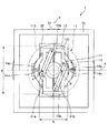
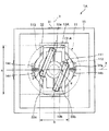
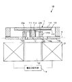
図1は、本発明の光スキャナー(光学デバイス)の第1実施形態を示す平面図、図2は、図1に示す光スキャナーの断面図(X軸に沿った断面図)、図3は、図1に示す光スキャナーが備える駆動手段の電圧印加手段を説明するためのブロック図、図4は、図3に示す第1の電圧発生部および第2の電圧発生部での発生電圧の一例を示す図である。なお、以下では、説明の便宜上、図2中の上側を「上」、下側を「下」と言う。
DESCRIPTION OF EXEMPLARY EMBODIMENTS Hereinafter, preferred embodiments of an optical device, an optical scanner, and an image display device of the invention will be described with reference to the accompanying drawings. In the following embodiments, a case where the optical device of the present invention is applied to an optical scanner will be representatively described.
<First Embodiment>
1 is a plan view showing a first embodiment of an optical scanner (optical device) of the present invention, FIG. 2 is a cross-sectional view (cross-sectional view along the X axis) of the optical scanner shown in FIG. 1, and FIG. FIG. 4 is a block diagram for explaining voltage applying means of driving means included in the optical scanner shown in FIG. 1, and FIG. 4 is an example of voltages generated in the first voltage generating unit and the second voltage generating unit shown in FIG. FIG. In the following, for convenience of explanation, the upper side in FIG. 2 is referred to as “upper” and the lower side is referred to as “lower”.
図1および図2に示すように、光スキャナー1は、可動部11と、1対の軸部12a、12b(第1軸部)と、枠体部13と、2対の軸部14a、14b、14c、14d(第2軸部)と、支持部15と、永久磁石21a、21bと、コイル31と、磁心32と、電圧印加手段4とを備える。
ここで、可動部11、1対の軸部12a、12bは、軸部12a、12bを軸としてY軸(第1の軸)周りに揺動(往復回動)する第1の振動系を構成する。また、可動部11、1対の軸部12a、12b、枠体部13、2対の軸部14a、14b、14c、14dおよび永久磁石21a、21bは、2対の軸部14a、14b、14c、14dを軸としてX軸(第2の軸)周りに揺動(往復回動)する第2の振動系を構成する。
また、永久磁石21a、21b、コイル31および電圧印加手段4は、前述した第1の振動系および第2の振動系を駆動(すなわち、可動部11をX軸およびY軸周りに揺動)させる駆動手段を構成する。
As shown in FIGS. 1 and 2, the
Here, the
Further, the
以下、光スキャナー1の各部を順次詳細に説明する。
可動部11は、基部111と、スペーサー112を介して基部111に固定された光反射板113とを有する。
光反射板113の上面(一方の面)には、光反射性を有する光反射部114が設けられている。
Hereinafter, each part of the
The
A
この光反射板113は、軸部12a、12bに対して厚さ方向に離間するとともに、厚さ方向からみたときに(以下、「平面視」ともいう)軸部12a、12bと重なって設けられている。
そのため、軸部12aと軸部12bとの間の距離を短くしつつ、光反射板113の板面の面積を大きくすることができる。また、軸部12aと軸部12bとの間の距離を短くすることができることから、枠体部13の小型化を図ることができる。さらに、枠体部13の小型化を図ることができることから、軸部14a、14bと軸部14c、14dとの間の距離を短くすることができる。
The
Therefore, the area of the plate surface of the
このようなことから、光反射板113の板面の面積を大きくしても、光スキャナー1の小型化を図ることができる。
また、光反射板113が軸部12a、12bに対して厚さ方向に離間して設けられているので、すなわち、軸部12a、12bが光反射板113の側面に直接接続されていないので、光反射板113の回動時に、軸部12a、12bの捩れ変形による応力が光反射板113に及ぶのを防止または抑制することができ、その結果、光反射板113の撓みを低減することができる。
For this reason, even if the area of the plate surface of the
Further, since the
また、永久磁石21a、21bは、枠体部13の光反射板113側の面に固定されている。したがって、永久磁石21a、21bが枠体部13の光反射板113と反対側の面に固定されている場合と比較して、例えば、図2における光スキャナー1の上下方向長さを短くすることが可能なので、光スキャナーの小型化を図ることができる。
また、光反射板113は、平面視にて、軸部12a、12bの全体を覆うように形成されている。言い換えると、軸部12a、12bは、それぞれ、平面視にて、光反射板113の外周に対して内側に位置している。これにより、光反射板113の板面の面積が大きくなり、その結果、光反射部114の面積を大きくすることができる。また、不要な光が軸部12a、12bで反射して迷光となるのを防止することができる。
The
Further, the
また、光反射板113は、平面視にて、枠体部13の全体を覆うように形成されている。言い換えると、枠体部13は、平面視にて、光反射板113の外周に対して内側に位置している。これにより、光反射板113の板面の面積が大きくなり、その結果、光反射部114の面積を大きくすることができる。また、不要な光が枠体部13で反射して迷光となるのを防止することができる。
The
さらに、光反射板113は、平面視にて、軸部14a、14b、14c、14dの全体を覆うように形成されている。言い換えると、軸部14a、14b、14c、14dは、それぞれ、平面視にて、光反射板113の外周に対して内側に位置している。これにより、光反射板113の板面の面積が大きくなり、その結果、光反射部114の面積を大きくすることができる。また、不要な光が軸部14a、14b、14c、14dで反射して迷光となるのを防止することができる。
Furthermore, the
本実施形態では、光反射板113は、平面視にて、円形をなしている。なお、光反射板113の平面視形状は、これに限定されず、例えば、楕円形、四角形等の多角形であってもよい。
このような光反射板113の下面(他方の面)には、硬質層115が設けられている。
硬質層115は、光反射板113本体の構成材料よりも硬質な材料で構成されている。これにより、光反射板113の剛性を高めることができる。そのため、光反射板113の揺動時における撓みを防止または抑制することができる。また、光反射板113の厚さを薄くし、光反射板113のX軸およびY軸周りの揺動時における慣性モーメントを抑えることができる。
In the present embodiment, the
A
The
このような硬質層115の構成材料としては、光反射板113本体の構成材料よりも硬質な材料であれば、特に限定されず、例えば、ダイヤモンド、カーボンナイトライド膜、水晶、サファイヤ、タンタル酸リチウム、ニオブ酸カリウムなどを用いることができるが、特に、ダイヤモンドを用いるのが好ましい。
硬質層115の厚さ(平均)は、特に限定されないが、1〜10μm程度であるのが好ましく、1〜5μm程度であるのがさらに好ましい。
The constituent material of the
The thickness (average) of the
また、硬質層115は、単層で構成されていてもよいし、複数の層の積層体で構成されていてもよい。なお、硬質層115は、必要に応じて設けられるものであり、省略することもできる。
このような硬質層115の形成には、例えば、プラズマCVD、熱CVD、レーザーCVDのような化学蒸着法(CVD)、真空蒸着、スパッタリング、イオンプレーティング等の乾式メッキ法、電解メッキ、浸漬メッキ、無電解メッキ等の湿式メッキ法、溶射、シート状部材の接合等を用いることができる。
Moreover, the
The
また、光反射板113の下面は、スペーサー112を介して基部111に固定されている。これにより、軸部12a、12b、枠体部13および軸部14a、14b、14c、14dとの接触を防止しつつ、光反射板113をY軸周りに揺動させることができる。
また、基部111は、それぞれ、平面視にて、光反射板113の外周に対して内側に位置している。また、基部111の平面視での面積は、基部111がスペーサー112を介して光反射板113を支持することができれば、できるだけ小さいのが好ましい。これにより、光反射板113の板面の面積を大きくしつつ、軸部12aと軸部12bとの間の距離を小さくすることができる。
In addition, the lower surface of the
In addition, each of the
枠体部13は、枠状をなし、前述した可動部11の基部111を囲んで設けられている。言い換えると、可動部11の基部111は、枠状をなす枠体部13の内側に設けられている。
そして、枠体部13は、軸部14a、14b、14c、14dを介して支持部15に支持されている。また、可動部11の基部111は、軸部12a、12bを介して枠体部13に支持されている。
The
And the
また、枠体部13は、Y軸に沿った方向での長さがX軸に沿った方向での長さよりも長くなっている。すなわち、Y軸に沿った方向における枠体部13の長さをaとし、X軸に沿った方向における枠体部13の長さをbとしたとき、a>bなる関係を満たす。これにより、軸部12a、12bに必要な長さを確保しつつ、X軸に沿った方向における光スキャナー1の長さを抑えることができる。
Further, the
また、枠体部13は、平面視にて、可動部11の基部111および1対の軸部12a、12bからなる構造体の外形に沿った形状をなしている。これにより、可動部11、1対の軸部12a、12bおよび永久磁石21a、21bで構成された第1の振動系の振動、すなわち、可動部11のY軸周りの揺動を許容しつつ、枠体部13の小型化を図ることができる。
なお、枠体部13の形状は、枠状であれば、図示のものに限定されない。
Moreover, the
In addition, if the shape of the
軸部12a、12bおよび軸部14a、14b、14c、14dは、それぞれ、弾性変形可能である。
そして、軸部12a、12bは、可動部11をY軸(第1の軸)周りに回動(揺動)可能とするように、可動部11と枠体部13を連結している。また、軸部14a、14b、14c、14dは、枠体部13をY軸に直交するX軸(第2の軸)周りに回動(揺動)可能とするように、枠体部13と支持部15を連結している。
The
The
軸部12a、12bは、可動部11の基部111を介して互いに対向するように配置されている。また、軸部12a、12bは、それぞれ、Y軸に沿った方向に延在する長手形状をなす。そして、軸部12a、12bは、それぞれ、一端部が基部111に接続され、他端部が枠体部13に接続されている。また、軸部12a、12bは、それぞれ、中心軸がY軸に一致するように配置されている。
The
このような軸部12a、12bは、それぞれ、可動部11のY軸周りの揺動に伴ってねじれ変形する。
軸部14a、14bおよび軸部14c、14dは、枠体部13を介して互いに対向するように配置されている。また、軸部14a、14b、14c、14dは、それぞれ、X軸に沿った方向に延在する長手形状をなす。そして、軸部14a、14b、14c、14dは、それぞれ、一端部が枠体部13に接続され、他端部が支持部15に接続されている。また、軸部14a、14bは、X軸を介して互いに対向するように配置され、同様に、軸部14c、14dは、X軸を介して互いに対向するように配置されている。
Each of the
The
このような軸部14a、14b、14c、14dは、枠体部13のX軸周りの揺動に伴って、軸部14a、14b全体および軸部14c、14d全体がそれぞれねじれ変形する。
このように、可動部11をY軸周りに揺動可能とするとともに、枠体部13をX軸周りに揺動可能とすることにより、可動部11を互いに直交するX軸およびY軸の2軸周りに揺動(回動)させることができる。
In
As described above, the
なお、軸部12a、12bおよび軸部14a、14b、14c、14dの形状は、それぞれ、前述したものに限定されず、例えば、途中の少なくとも1箇所に屈曲または湾曲した部分や分岐した部分を有していてもよい。
前述したような基部111、軸部12a、12b、枠体部13、軸部14a、14b、14c、14dおよび支持部15は、一体的に形成されている。
The shapes of the
The
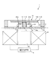
本実施形態では、基部111、軸部12a、12b、枠体部13、軸部14a、14b、14c、14dおよび支持部15は、第1のSi層(デバイス層)と、SiO2層(ボックス層)と、第2のSi層(ハンドル層)とがこの順に積層したSOI基板をエッチングすることにより形成されている。これにより、第1の振動系および第2の振動系の振動特性を優れたものとすることができる。また、SOI基板は、エッチングにより微細な加工が可能であるため、SOI基板を用いて基部111、軸部12a、12b、枠体部13、軸部14a、14b、14c、14dおよび支持部15を形成することにより、これらの寸法精度を優れたものとすることができ、また、光スキャナー1の小型化を図ることができる。
In the present embodiment, the
そして、基部111、軸部12a、12bおよび軸部14a、14b、14c、14dは、それぞれ、SOI基板の第1のSi層で構成されている。これにより、軸部12a、12bおよび軸部14a、14b、14c、14dの弾性を優れたものとすることができる。また、基部111がY軸周りに回動する際に枠体部13に接触するのを防止することができる。
The
また、枠体部13および支持部15は、それぞれ、SOI基板の第1のSi層、SiO2層および第2のSi層からなる積層体で構成されている。これにより、枠体部13および支持部15の剛性を優れたものとすることができる。また、枠体部13のSiO2層および第2のSi層は、リブ131を構成する。
このようにSOI基板のデバイス層を用いて形成された基部111のハンドル層側(枠体部13および支持部15が突出する側)には、光反射板113が設けられている。これにより、基部111、枠体部13、軸部12a、12bおよび軸部14a、14b、14c、14dを含む構造体の光反射板113とは反対側の面を平坦な面とすることができる。そのため、枠体部13に対する永久磁石21a、21bの設置の際、および、基部111に対する光反射板113の設置の際に、簡単な構成の治具を用いて枠体部13および基部111を支持することができる。
Further, the
Thus, the
また、枠体部13に光反射板113側(上側)に突出するリブ131が形成されているので、枠体部13の剛性を高めることができる。また、リブ131が光反射板113側に突出しているので、枠体部13の光反射板113とは反対側の面と、基部111の光反射板113とは反対側の面とを同一面に沿って形成することができる。そのため、枠体部13に対する永久磁石21a、21bの設置の際、および、基部111に対する光反射板113の設置の際に、簡単な構成の治具を用いて枠体部13および基部111を支持することができる。
In addition, since the
また、支持部15の上面には、反射防止処理が施されているのが好ましい。これにより、支持部15に照射された不要光が迷光となるのを防止することができる。
かかる反射防止処理としては、特に限定されないが、例えば、反射防止膜(誘電体多層膜)の形成、粗面化処理、黒色処理等が挙げられる。
なお、前述した基部111、軸部12a、12bおよび軸部14a、14b、14c、14dの構成材料および形成方法は、一例であり、本発明は、これに限定されるものではない。
Further, the upper surface of the
Such an antireflection treatment is not particularly limited, and examples thereof include formation of an antireflection film (dielectric multilayer film), roughening treatment, and black treatment.
Note that the above-described constituent materials and forming methods of the
また、本実施形態では、スペーサー112および光反射板113も、SOI基板をエッチングすることにより形成されている。そして、スペーサー112は、SOI基板のSiO2層および第2のSi層からなる積層体で構成されている。また、光反射板113は、SOI基板の第1のSi層で構成されている。
このように、SOI基板を用いてスペーサー112および光反射板113を形成することにより、互いに接合されたスペーサー112および光反射板113を簡単かつ高精度に製造することができる。
In this embodiment, the
Thus, by forming the
このようなスペーサー112は、例えば、接着剤、ろう材等の接合材(図示せず)により基部111に接合されている。なお、基部111に対するスペーサー112の接合(設置)は、枠体部13に対する永久磁石21a、21bの接合(設置)後に行われる。
前述した枠体部13の上面(光反射板113側の面)には、永久磁石21a、21bが接合・固定されている。これにより、枠体部13に対する永久磁石21a、21bの設置、および、基部111に対する光反射板113の設置を容易なものとすることができる。
Such a
永久磁石21a、21bと枠体部13との接合方法としては、特に限定されないが、例えば、接着剤を用いた接合方法を用いることができる。
本実施形態では、永久磁石21a、21bは、枠体部13のリブ131の頂面(上面)に固定されている。これにより、リブ131がスペーサーとしても機能し、基部111が永久磁石21a、21bに接触するのを防止しつつ、可動部11をY軸周りに揺動させることができる。
Although it does not specifically limit as a joining method of
In the present embodiment, the
また、永久磁石21a、21bは、平面視にて、可動部11のスペーサー112に重ならないように設けられている。これにより、軸部12a、12b、枠体部13、軸部14a、14b、14c、14dおよび永久磁石21a、21bとの接触を防止しつつ、光反射板113を揺動させることができる。
また、1対の永久磁石21a、21bは、スペーサー112を介して対向している。これにより、枠体部13を第2の軸周りに円滑に揺動させることができる。
Further, the
The pair of
永久磁石21a、21bは、それぞれ、平面視にて、一方の磁極と他方の磁極とがX軸を挟んで配置されるとともに、X軸およびY軸に対して傾斜する方向に磁化されている。
本実施形態では、永久磁石21a、21bは、それぞれ、X軸およびY軸に対して傾斜する方向に延在する長手形状(棒状)をなす。そして、永久磁石21a、21bは、それぞれ、長手方向に磁化されている。すなわち、永久磁石21a、21bは、それぞれ、一端部をS極とし、他端部をN極とするように磁化されている。
Each of the
In the present embodiment, the
また、平面視にて、永久磁石21aの一方(図1にて上側)の端部(N極)がY軸上に配置されている。同様に、永久磁石21bの一方(図1にて下側)の端部(S極)がY軸上に配置されている。これにより、光反射板113をX軸周りに円滑に揺動させることができる。
また、永久磁石21a、21bは、平面視にて、X軸とY軸との交点を中心として対称(点対称)となるように設けられている。
Further, one end (N pole) of the
Further, the
X軸に対する永久磁石21a、21bの磁化の方向(延在方向)の傾斜角θは、それぞれ、特に限定されないが、30°以上60°以下であるのが好ましく、45°以上60°以下であることがより好ましく、45°であるのがさらに好ましい。このように永久磁石21a、21bを設けることで、円滑かつ確実に可動部11をX軸の周りに回動させることができる。
これに対し、傾斜角θが前記下限値未満であると、電圧印加手段4によりコイル31に印加される電圧の強さなどの諸条件によっては、可動部11を十分にX軸周りに回動させることができない場合がある。一方、傾斜角θが前記上限値を超えると、諸条件によっては、可動部11を十分にY軸周りに回動させることができない場合がある。
The inclination angle θ of the magnetization direction (extending direction) of the
On the other hand, if the inclination angle θ is less than the lower limit value, the
このような永久磁石21a、21bとしては、それぞれ、例えば、ネオジム磁石、フェライト磁石、サマリウムコバルト磁石、アルニコ磁石、ボンド磁石等を好適に用いることができる。このような永久磁石21a、21bは、それぞれ、硬磁性体を着磁したものであり、例えば、着磁前の硬磁性体を枠体部13に設置した後に着磁することにより形成される。既に着磁がなされた永久磁石21a、21bを枠体部13に設置しようとすると、永久磁石21a、21b同士の磁界や、外部の磁界の影響により、永久磁石21a、21bを所望の位置に設置できない場合があるからである。
As such
永久磁石21a、21bの直下には、コイル31が設けられている。すなわち、枠体部13の下面に対向するように、コイル31が設けられている。これにより、コイル31から発生する磁界を効率的に永久磁石21a、21bに作用させることができる。これにより、光スキャナー1の省電力化および小型化を図ることができる。
本実施形態では、コイル31は、磁心32に巻回されて設けられている。これにより、コイル31で発生した磁界を効率的に永久磁石21a、21bに作用させることができる。なお、磁心32は、省略してもよい。
A
In the present embodiment, the
このようなコイル31は、電圧印加手段4に電気的に接続されている。
そして、電圧印加手段4によりコイル31に電圧が印加されることで、コイル31からX軸およびY軸に直交する磁束を有する磁界が発生する。
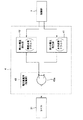
電圧印加手段4は、図3に示すように、可動部11をY軸周りに回動させるための第1の電圧V1を発生させる第1の電圧発生部41と、可動部11をX軸周りに回動させるための第2の電圧V2を発生させる第2の電圧発生部42と、第1の電圧V1と第2の電圧V2とを重畳する電圧重畳部43とを備え、電圧重畳部43で重畳した電圧をコイル31に印加する。
Such a
Then, a voltage is applied to the
As shown in FIG. 3, the voltage applying means 4 includes a
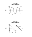
第1の電圧発生部41は、図4(a)に示すように、周期T1で周期的に変化する第1の電圧V1(水平走査用電圧)を発生させるものである。すなわち、第1の電圧発生部41は、第1周波数(1/T1)の第1の電圧V1を発生させるものである。
第1の電圧V1は、正弦波のような波形をなしている。そのため、光スキャナー1は効果的に光を主走査することができる。なお、第1の電圧V1の波形は、これに限定されない。
As shown in FIG. 4A, the
The first voltage V1 has a waveform like a sine wave. Therefore, the
また、第1周波数(1/T1)は、水平走査に適した周波数であれば、特に限定されないが、10〜40kHzであるのが好ましい。
本実施形態では、第1周波数は、可動部11、1対の軸部12a、12bで構成される第1の振動系(ねじり振動系)のねじり共振周波数(f1)と等しくなるように設定されている。つまり、第1の振動系は、そのねじり共振周波数f1が水平走査に適した周波数になるように設計(製造)されている。これにより、可動部11のY軸周りの回動角を大きくすることができる。
The first frequency (1 / T1) is not particularly limited as long as it is suitable for horizontal scanning, but is preferably 10 to 40 kHz.
In the present embodiment, the first frequency is set to be equal to the torsional resonance frequency (f1) of the first vibration system (torsional vibration system) composed of the
一方、第2の電圧発生部42は、図4(b)に示すように、周期T1と異なる周期T2で周期的に変化する第2の電圧V2(垂直走査用電圧)を発生させるものである。すなわち、第2の電圧発生部42は、第2周波数(1/T2)の第2の電圧V2を発生させるものである。
第2の電圧V2は、鋸波のような波形をなしている。そのため、光スキャナー1は効果的に光を垂直走査(副走査)することができる。なお、第2の電圧V2の波形は、これに限定されない。
On the other hand, as shown in FIG. 4B, the
The second voltage V2 has a sawtooth waveform. Therefore, the
第2周波数(1/T2)は、第1周波数(1/T1)と異なり、かつ、垂直走査に適した周波数であれば、特に限定されないが、30〜120Hz(60Hz程度)であるのが好ましい。このように、第2の電圧V2の周波数を60Hz程度とし、前述したように第1の電圧V1の周波数を10〜40kHzとすることで、ディスプレイでの描画に適した周波数で、可動部11を互いに直交する2軸(X軸およびY軸)のそれぞれの軸周りに回動させることができる。ただし、可動部11をX軸およびY軸のそれぞれの軸周りに回動させることができれば、第1の電圧V1の周波数と第2の電圧V2の周波数との組み合わせは、特に限定されない。
The second frequency (1 / T2) is not particularly limited as long as it is different from the first frequency (1 / T1) and is suitable for vertical scanning, but is preferably 30 to 120 Hz (about 60 Hz). . As described above, the frequency of the second voltage V2 is set to about 60 Hz, and the frequency of the first voltage V1 is set to 10 to 40 kHz as described above, so that the
本実施形態では、第2の電圧V2の周波数は、可動部11、1対の軸部12a、12b、枠体部13、2対の軸部14a、14b、14c、14dおよび永久磁石21a、21bで構成された第2の振動系(ねじり振動系)のねじり共振周波数(共振周波数)と異なる周波数となるように調整されている。
このような第2の電圧V2の周波数(第2周波数)は、第1の電圧V1の周波数(第1周波数)よりも小さいことが好ましい。すなわち、周期T2は、周期T1よりも長いことが好ましい。これにより、より確実かつより円滑に、可動部11をY軸周りに第1周波数で回動させつつ、X軸周りに第2周波数で回動させることができる。
In the present embodiment, the frequency of the second voltage V2 includes the
The frequency (second frequency) of the second voltage V2 is preferably smaller than the frequency (first frequency) of the first voltage V1. That is, the period T2 is preferably longer than the period T1. Thereby, the
また、第1の振動系のねじり共振周波数をf1[Hz]とし、第2の振動系のねじり共振周波数をf2[Hz]としたとき、f1とf2とが、f2<f1の関係を満たすことが好ましく、f1≧10f2の関係を満たすことがより好ましい。これにより、より円滑に、可動部11を、Y軸周りに第1の電圧V1の周波数で回動させつつ、X軸周りに第2の電圧V2の周波数で回動させることができる。これに対し、f1≦f2とした場合は、第2周波数による第1の振動系の振動が起こる可能性がある。
Further, when the torsional resonance frequency of the first vibration system is f1 [Hz] and the torsional resonance frequency of the second vibration system is f2 [Hz], f1 and f2 satisfy the relationship of f2 <f1. Is preferable, and it is more preferable to satisfy the relationship of f1 ≧ 10f2. Thereby, the
このような第1の電圧発生部41および第2の電圧発生部42は、それぞれ、制御部7に接続され、この制御部7からの信号に基づき駆動する。このような第1の電圧発生部41および第2の電圧発生部42には、電圧重畳部43が接続されている。
電圧重畳部43は、コイル31に電圧を印加するための加算器43aを備えている。加算器43aは、第1の電圧発生部41から第1の電圧V1を受けるとともに、第2の電圧発生部42から第2の電圧V2を受け、これらの電圧を重畳しコイル31に印加するようになっている。
The first
The
次に、光スキャナー1の駆動方法について説明する。なお、本実施形態では、前述したように、第1の電圧V1の周波数は、第1の振動系のねじり共振周波数と等しく設定されており、第2の電圧V2の周波数は、第2の振動系のねじり共振周波数と異なる値に、かつ、第1の電圧V1の周波数よりも小さくなるように設定されている(例えば、第1の電圧V1の周波数が18kHz、第2の電圧V2の周波数が60Hzに設定されている)。
Next, a method for driving the
例えば、図4(a)に示すような第1の電圧V1と、図4(b)に示すような第2の電圧V2とを電圧重畳部43にて重畳し、重畳した電圧をコイル31に印加する。
すると、第1の電圧V1によって、永久磁石21a、21bの一端部(N極)をコイル31に引き付けようとするとともに、永久磁石21a、21bの他端部(S極)をコイル31から離間させようとする磁界(この磁界を「磁界A1」という)と、永久磁石21a、21bの一端部(N極)をコイル31から離間させようとするとともに、永久磁石21a、21bの他端部(S極)をコイル31に引き付けようとする磁界(この磁界を「磁界A2」という)とが交互に切り換わる。
For example, the
Then, the first voltage V1 tries to attract one end (N pole) of the
ここで、図1の平面視において、Y軸を挟んで一方側に永久磁石21aのS極が位置し、他方側に永久磁石21bのN極が位置している。そのため、磁界A1と磁界A2とが交互に切り換わることで、枠体部13にY軸周りのねじり振動成分を有する振動が励振され、その振動に伴って、軸部12a、12bを捩れ変形させつつ、可動部11が第1の電圧V1の周波数でY軸まわりに回動する。
また、第1の電圧V1の周波数は、第1の振動系のねじり共振周波数と等しい。そのため、第1の電圧V1によって、効率的に、可動部11をY軸周りに回動させることができる。すなわち、前述した枠体部13のY軸周りのねじり振動成分を有する振動が小さくても、その振動に伴う可動部11のY軸周りの回動角を大きくすることができる。
Here, in the plan view of FIG. 1, the south pole of the
The frequency of the first voltage V1 is equal to the torsional resonance frequency of the first vibration system. Therefore, the
一方、第2の電圧V2によって、永久磁石21a、21bの一端部(N極)をコイル31に引き付けようとするとともに、永久磁石21a、21bの他端部(S極)をコイル31から離間させようとする磁界(この磁界を「磁界B1」という)と、永久磁石21a、21bの一端部(N極)をコイル31から離間させようとするとともに、永久磁石21a、21bの他端部(S極)をコイル31に引き付けようとする磁界(この磁界を「磁界B2」という)とが交互に切り換わる。
On the other hand, the second voltage V2 tries to attract one end (N pole) of the
ここで、図1の平面視において、X軸を挟んで一方側に永久磁石21a、21bのN極が位置し、他方側に永久磁石21a、21bのS極が位置している。そのため、磁界B1と磁界B2とが交互に切り換わることで、軸部14a、14bおよび軸部14c、14dをそれぞれ捩れ変形させつつ、枠体部13が可動部11とともに、第2の電圧V2の周波数でX軸周りに回動する。
また、第2の電圧V2の周波数は、第1の電圧V1の周波数に比べて極めて低く設定されている。また、第2の振動系のねじり共振周波数は、第1の振動系のねじり共振周波数よりも低く設計されている。そのため、可動部11が第2の電圧V2の周波数でY軸周りに回動してしまうことを防止することができる。
Here, in the plan view of FIG. 1, the north poles of the
Further, the frequency of the second voltage V2 is set to be extremely lower than the frequency of the first voltage V1. The torsional resonance frequency of the second vibration system is designed to be lower than the torsional resonance frequency of the first vibration system. Therefore, it is possible to prevent the
以上説明したように光スキャナー1では、第1の電圧V1と第2の電圧V2とを重畳させた電圧をコイル31に印加することで、可動部11を、Y軸周りに第1の電圧V1の周波数で回動させつつ、X軸周りに第2の電圧V2の周波数で回動させることができる。これにより、装置の低コスト化および小型化を図るとともに、電磁駆動方式(ムービングマグネット方式)により、可動部11をX軸およびY軸のそれぞれの軸周りに回動させることができる。また、駆動源を構成する部品(永久磁石およびコイル)の数を少なくすることができるため、簡単かつ小型な構成とすることができる。また、コイル31が光スキャナー1の振動系と離間しているので、かかる振動系に対するコイル31の発熱による悪影響を防止することができる。
As described above, in the
特に、光反射板113が軸部12a、12bに対して厚さ方向に離間するとともに厚さ方向からみたときに軸部12a、12bと重なって設けられているので、光スキャナー1の小型化を図ることができる。
また、枠体部13の光反射板113側の面に永久磁石21a、21bが固定されているので、枠体部13に対する永久磁石21a、21bの設置、および、基部111に対する光反射板113の設置を容易なものとすることができる。
In particular, since the
Further, since the
<第2実施形態>
次に、本発明の第2実施形態について説明する。
図5は、本発明の光スキャナー(光学デバイス)の第2実施形態を示す平面図、図6は、図5に示す光スキャナーの断面図(X軸に沿った断面図)である。なお、以下では、説明の便宜上、図6中の上側を「上」、下側を「下」と言う。
Second Embodiment
Next, a second embodiment of the present invention will be described.
FIG. 5 is a plan view showing a second embodiment of the optical scanner (optical device) of the present invention, and FIG. 6 is a cross-sectional view (cross-sectional view along the X axis) of the optical scanner shown in FIG. In the following, for convenience of explanation, the upper side in FIG. 6 is referred to as “upper” and the lower side is referred to as “lower”.
以下、第2実施形態について、前述した第1実施形態との相違点を中心に説明し、同様の事項については、その説明を省略する。なお、図5および図6において、前述した実施形態と同様の構成については、同一符号を付している。
本実施形態の光スキャナーは、枠体部および永久磁石の構成(形状)が異なる以外は、前述した第1実施形態の光スキャナーと同様である。
Hereinafter, the second embodiment will be described with a focus on the differences from the first embodiment described above, and the description of the same matters will be omitted. 5 and 6, the same reference numerals are given to the same configurations as those in the above-described embodiment.
The optical scanner of the present embodiment is the same as the optical scanner of the first embodiment described above except that the configuration (shape) of the frame and the permanent magnet is different.
図5に示すように、第2実施形態の光スキャナー1Aは、枠体部13Aおよび永久磁石22a、22bを備える。
枠体部13Aは、枠状をなし、可動部11の基部111を囲んで設けられている。
そして、枠体部13Aは、軸部14a、14b、14c、14dを介して支持部15に支持されている。また、可動部11の基部111は、軸部12a、12bを介して枠体部13Aに支持されている。
As shown in FIG. 5, the
The
The
本実施形態では、枠体部13Aは、リブ131Aを有する。
このリブ131Aは、枠体部13Aの厚さ方向からみたとき、永久磁石22a、22bと重ならない領域に形成されている。これにより、X軸周りの振動系(第2の振動系)の重心をX軸に近づけることができる。その結果、光反射板113をX軸周りに円滑に揺動させることができる。
In the present embodiment, the
The
また、リブ131Aは、枠体部13Aの厚さ方向に対して垂直な方向(X軸およびY軸に平行な方向)における永久磁石22a、22bの移動を規制するように形成されている。言い換えると、リブ131Aは、平面視にて、永久磁石22a、22bの外形に沿って形成された部分(ガイド部)を有する。これにより、枠体部13Aに対する永久磁石22a、22bの設置を容易なものとすることができる。
The
このようなリブ131Aは、永久磁石22a、22bが設置される領域を除くように、SOI基板のハンドル層およびボックス層を加工することにより形成されている。
そして、永久磁石22a、22bは、枠体部13Aのデバイス層で構成された部分に固定されている。
本実施形態では、永久磁石22aの基部111と対向する部分には、凹部221aが形成されている。同様に、永久磁石22bの基部111と対向する部分には、凹部221bが形成されている。このような凹部221a、221bを形成することにより、基部111が永久磁石22a、22bと接触するのを防止することができる。
以上説明したような第2実施形態の光スキャナー1Aによっても、小型化を図りつつ、2次元的に光を走査することができる。
And
In the present embodiment, a
The
<第3実施形態>
次に、本発明の第3実施形態について説明する。
図7は、本発明の光スキャナー(光学デバイス)の第3実施形態を示す平面図、図8は、図7に示す光スキャナーの断面図(X軸に沿った断面図)である。なお、以下では、説明の便宜上、図8中の上側を「上」、下側を「下」と言う。
<Third Embodiment>
Next, a third embodiment of the present invention will be described.
FIG. 7 is a plan view showing a third embodiment of the optical scanner (optical device) of the present invention, and FIG. 8 is a cross-sectional view (cross-sectional view along the X axis) of the optical scanner shown in FIG. In the following, for convenience of explanation, the upper side in FIG. 8 is referred to as “upper” and the lower side is referred to as “lower”.
以下、第3実施形態について、前述した第1実施形態との相違点を中心に説明し、同様の事項については、その説明を省略する。なお、図7および図8において、前述した実施形態と同様の構成については、同一符号を付している。
本実施形態の光スキャナーは、枠体部および永久磁石の構成(形状)が異なる以外は、前述した第1実施形態の光スキャナーと同様である。
Hereinafter, the third embodiment will be described with a focus on differences from the first embodiment described above, and descriptions of the same matters will be omitted. 7 and 8, the same reference numerals are given to the same configurations as those in the above-described embodiment.
The optical scanner of the present embodiment is the same as the optical scanner of the first embodiment described above except that the configuration (shape) of the frame and the permanent magnet is different.
図7に示すように、第3実施形態の光スキャナー1Bは、枠体部13Bおよび永久磁石23a、23bを備える。
枠体部13Bは、枠状をなし、可動部11の基部111を囲んで設けられている。
そして、枠体部13Bは、軸部14a、14b、14c、14dを介して支持部15に支持されている。また、可動部11の基部111は、軸部12a、12bを介して枠体部13Bに支持されている。
As shown in FIG. 7, the
The
The
本実施形態では、枠体部13Bは、リブ131Bを有する。
このリブ131Bは、枠体部13Bの厚さ方向からみたとき、永久磁石23a、23bと重ならない領域に形成されている。これにより、X軸周りの振動系の重心をX軸に近づけることができる。その結果、光反射板113をX軸周りに円滑に揺動させることができる。
In the present embodiment, the
The
また、リブ131Bは、枠体部13Bの厚さ方向に対して垂直な方向における永久磁石23a、23bの移動を規制するように形成されている。これにより、枠体部13Bに対する永久磁石23a、23bの設置を容易なものとすることができる。
本実施形態では、永久磁石23a、23bは、平面視にて、可動部11の基部111に重ならないように設けられている。これにより、基部111が永久磁石23a、23bに接触するのを防止することができる。
以上説明したような第3実施形態の光スキャナー1Bによっても、小型化を図りつつ、2次元的に光を走査することができる。
The
In the present embodiment, the
The
<画像表示装置の実施形態>
図9は、本発明の画像表示装置の実施形態を模式的に示す図である。
本実施形態では、画像表示装置の一例として、光スキャナー1をイメージング用ディスプレイの光スキャナーとして用いた場合を説明する。なお、スクリーンSの長手方向を「横方向」といい、長手方向に直角な方向を「縦方向」という。また、X軸がスクリーンSの横方向と平行であり、Y軸がスクリーンSの縦方向と平行である。
<Embodiment of Image Display Device>
FIG. 9 is a diagram schematically showing an embodiment of the image display device of the present invention.
In the present embodiment, a case where the
画像表示装置(プロジェクター)9は、レーザーなどの光を照出する光源装置(光源)91と、複数のダイクロイックミラー92A、92B、92Cと、光スキャナー1とを有している。
光源装置91は、赤色光を照出する赤色光源装置911と、青色光を照出する青色光源装置912と、緑色光を照出する緑色光源装置913とを備えている。
The image display device (projector) 9 includes a light source device (light source) 91 that emits light such as a laser, a plurality of
The light source device 91 includes a red
各ダイクロイックミラー92A、92B、92Cは、赤色光源装置911、青色光源装置912、緑色光源装置913のそれぞれから照出された光を合成する光学素子である。
このような画像表示装置9は、図示しないホストコンピューターからの画像情報に基づいて、光源装置91(赤色光源装置911、青色光源装置912、緑色光源装置913)から照出された光をダイクロイックミラー92A、92B、92Cでそれぞれ合成し、この合成された光が光スキャナー1によって2次元走査され、スクリーンS上でカラー画像を形成するように構成されている。
The dichroic mirrors 92A, 92B, and 92C are optical elements that synthesize light emitted from the red
Such an
2次元走査の際、光スキャナー1の可動部11のY軸周りの回動により光反射部114で反射した光がスクリーンSの横方向に走査(主走査)される。一方、光スキャナー1の可動部11のX軸周りの回動により光反射部114で反射した光がスクリーンSの縦方向に走査(副走査)される。
なお、図9中では、ダイクロイックミラー92A、92B、92Cで合成された光を光スキャナー1によって2次元的に走査した後、その光を固定ミラー93で反射させてからスクリーンSに画像を形成するように構成されているが、固定ミラー93を省略し、光スキャナー1によって2次元的に走査された光を直接スクリーンSに照射してもよい。
During the two-dimensional scanning, the light reflected by the
In FIG. 9, the light synthesized by the
以下に、画像表示装置の応用例について説明する。
<画像表示装置の応用例1>
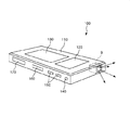
図10は、本発明の画像表示装置の応用例1を示す斜視図である。
図10に示すように、画像表示装置9は、携帯用画像表示装置100に適用することができる。
Hereinafter, application examples of the image display apparatus will be described.
<Application Example 1 of Image Display Device>
FIG. 10 is a perspective view showing an application example 1 of the image display device of the present invention.
As shown in FIG. 10, the
この携帯用画像表示装置100は、手で把持することができる寸法で形成されたケーシング110と、ケーシング110内に内蔵された画像表示装置9とを有している。この携帯用画像表示装置100により、例えば、スクリーンや、デスク上等の所定の面に、所定の画像を表示することができる。
また、携帯用画像表示装置100は、所定の情報を表示するディスプレイ120と、キーパット130と、オーディオポート140と、コントロールボタン150と、カードスロット160と、AVポート170とを有している。
なお、携帯用画像表示装置100は、通話機能、GSP受信機能等の他の機能を備えていてもよい。
The portable
In addition, the portable
Note that the portable
<画像表示装置の応用例2>
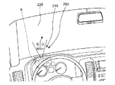
図11は、本発明の画像表示装置の応用例2を示す斜視図である。
図11に示すように、画像表示装置9は、ヘッドアップディスプレイシステム200に適用することができる。
このヘッドアップディスプレイシステム200では、画像表示装置9は、自動車のダッシュボードに、ヘッドアップディスプレイ210を構成するよう搭載されている。このヘッドアップディスプレイ210により、フロントガラス220に、例えば、目的地までの案内表示等の所定の画像を表示することができる。
なお、ヘッドアップディスプレイシステム200は、自動車に限らず、例えば、航空機、船舶等にも適用することができる。
<Application Example 2 of Image Display Device>
FIG. 11 is a perspective view showing an application example 2 of the image display device of the present invention.
As shown in FIG. 11, the
In the head-up
Note that the head-up
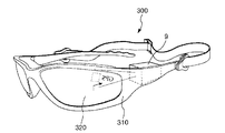
<画像表示装置の応用例3>
図12は、本発明の画像表示装置の応用例3を示す斜視図である。
図12に示すように、画像表示装置9は、ヘッドマウントディスプレイ300に適用することができる。
すなわち、ヘッドマウントディスプレイ300は、眼鏡310と、眼鏡310に搭載された画像表示装置9とを有している。そして、画像表示装置9により、眼鏡310の本来レンズである部位に設けられた表示部320に、一方の目で視認される所定の画像を表示する。
<Application Example 3 of Image Display Device>
FIG. 12 is a perspective view showing an application example 3 of the image display device of the present invention.
As shown in FIG. 12, the
That is, the head mounted
表示部320は、透明であってもよく、また、不透明であってもよい。表示部320が透明な場合は、現実世界からの情報に画像表示装置9からの情報を上乗せして使用することができる。
なお、ヘッドマウントディスプレイ300に、2つ画像表示装置9を設け、両方の目で視認される画像を、2つの表示部に表示するようにしてもよい。
The
Note that the head-mounted
以上、本発明の光学デバイス、光スキャナーおよび画像表示装置について、図示の実施形態に基づいて説明したが、本発明はこれに限定されるものではない。例えば、本発明の光学デバイス、光スキャナーおよび画像表示装置では、各部の構成は、同様の機能を有する任意の構成のものに置換することができ、また、他の任意の構成を付加することもできる。 Although the optical device, the optical scanner, and the image display apparatus of the present invention have been described based on the illustrated embodiments, the present invention is not limited to this. For example, in the optical device, the optical scanner, and the image display apparatus of the present invention, the configuration of each unit can be replaced with an arbitrary configuration having the same function, and other arbitrary configurations can be added. it can.
また、本発明は、前記各実施形態のうちの、任意の2以上の構成(特徴)を組み合わせたものであってもよい。
また、前述した実施形態では、第1軸部が2つ(1対)設けられている場合を例に説明したが、これに限定されず、例えば、第1軸部が4つ(2対)以上設けられていてもよい。
Further, the present invention may be a combination of any two or more configurations (features) of the above embodiments.
In the above-described embodiment, the case where two first shaft portions (one pair) are provided has been described as an example. However, the present invention is not limited to this. For example, four first shaft portions (two pairs) are provided. It may be provided above.
また、前述した実施形態では、第2軸部が4つ(2対)設けられている場合を例に説明したが、これに限定されず、例えば、第2軸部が2つ(1対)または6つ(3対)以上であってもよい。
また、前述した実施形態では、平面視にて光反射板が第1軸部全体、枠体部全体および第2軸部全体を覆う場合を例に説明したが、平面視にて光反射板が第1軸部の少なくとも一部(可動部の基部側の端部)が覆われていれば、前述したような光学デバイスの小型化、光反射板の大面積化、光反射板の動撓みの防止、第1軸部の基部側の端部による迷光の防止等の効果を奏することができる。
In the above-described embodiment, the case where four second shaft portions (two pairs) are provided has been described as an example. However, the present invention is not limited to this. For example, two second shaft portions (one pair) are provided. Or six (3 pairs) or more may be sufficient.
Moreover, although embodiment mentioned above demonstrated as an example the case where a light reflecting plate covered the whole 1st axial part, the whole frame part, and the whole 2nd axial part by planar view, a light reflecting plate is planar view. If at least a part of the first shaft portion (the end portion on the base side of the movable portion) is covered, the optical device as described above can be reduced in size, the light reflecting plate can be increased in area, and the light reflecting plate can be flexibly deformed. Effects such as prevention and prevention of stray light by the end of the first shaft portion on the base side can be achieved.
また、前述した実施形態では、SOI基板を加工することにより光反射板およびスペーサーを形成した場合を例に説明したが、これに限定されず、例えば、光反射板およびスペーサーを別々の基板から形成してもよい。
また、光反射板と基部との間のスペーサーは、ハンダボールであってもよい。この場合、例えば、光反射板および基部のスペーサー側の面にそれぞれ金属膜を形成しておき、これらの金属膜同士をハンダボールを介して接合すればよい。
In the above-described embodiment, the case where the light reflecting plate and the spacer are formed by processing the SOI substrate has been described as an example. However, the present invention is not limited to this. For example, the light reflecting plate and the spacer are formed from different substrates. May be.
The spacer between the light reflecting plate and the base may be a solder ball. In this case, for example, metal films may be formed on the light reflecting plate and the spacer side surfaces of the base, and these metal films may be bonded to each other via solder balls.
また、前述した実施形態では、本発明の光学デバイスを光スキャナーに適用した場合を例に説明したが、これに限定されず、本発明の光学デバイスは、例えば、光スイッチ、光アッテネータ等の他の光学デバイスにも適用可能である。
また、前述した実施形態では、枠体部の揺動および振動により可動部を互いに直交する2軸周りに回動させる場合を例に説明したが、本発明は、これに限定されず、例えば、可動部を第1の軸周りに回動させる手段を、枠体部を第2の軸周りに回動させる手段とは別途設けてもよい。この場合、可動部を第1の軸周りに回動させる手段としては、例えば、圧電駆動方式、電磁駆動方式、静電駆動方式等の公知の駆動方式を用いることができる。
In the above-described embodiment, the case where the optical device of the present invention is applied to an optical scanner has been described as an example. However, the present invention is not limited to this, and the optical device of the present invention includes, for example, an optical switch, an optical attenuator, and the like. The present invention can also be applied to other optical devices.
Further, in the above-described embodiment, the case where the movable part is rotated around two axes orthogonal to each other by the swing and vibration of the frame body part has been described as an example, but the present invention is not limited to this. The means for rotating the movable part around the first axis may be provided separately from the means for rotating the frame part around the second axis. In this case, as a means for rotating the movable portion around the first axis, for example, a known driving method such as a piezoelectric driving method, an electromagnetic driving method, an electrostatic driving method, or the like can be used.
1‥‥光スキャナー 1A‥‥光スキャナー 1B‥‥光スキャナー 4‥‥電圧印加手段 7‥‥制御部 9‥‥画像表示装置 11‥‥可動部 12a‥‥軸部 12b‥‥軸部 13‥‥枠体部 13A‥‥枠体部 13B‥‥枠体部 14a‥‥軸部 14b‥‥軸部 14c‥‥軸部 14d‥‥軸部 15‥‥支持部 21a‥‥永久磁石 21b‥‥永久磁石 22a‥‥永久磁石 22b‥‥永久磁石 23a‥‥永久磁石 23b‥‥永久磁石 31‥‥コイル 32‥‥磁心 41‥‥第1の電圧発生部 42‥‥第2の電圧発生部 43‥‥電圧重畳部 43a‥‥加算器 91‥‥光源装置 92A、92B、92C‥‥ダイクロイックミラー 93‥‥固定ミラー 100‥‥携帯用画像表示装置 110‥‥ケーシング 111‥‥基部 112‥‥スペーサー 113‥‥光反射板 114‥‥光反射部 115‥‥硬質層 120‥‥ディスプレイ 130‥‥キーパット 131‥‥リブ 131A‥‥リブ 131B‥‥リブ 140‥‥オーディオポート 150‥‥コントロールボタン 160‥‥カードスロット 170‥‥ポート 200‥‥ヘッドアップディスプレイシステム 210‥‥ヘッドアップディスプレイ 220‥‥フロントガラス 221a‥‥凹部 221b‥‥凹部 300‥‥ヘッドマウントディスプレイ 310‥‥眼鏡 320‥‥表示部 911‥‥赤色光源装置 912‥‥青色光源装置 913‥‥緑色光源装置 S‥‥スクリーン T1‥‥周期 T2‥‥周期 V1‥‥第1の電圧 V2‥‥第2の電圧 θ‥‥傾斜角
DESCRIPTION OF
Claims (16)
前記第1の軸に交差する第2の軸周りに揺動可能な枠体部と、
前記可動部を前記枠体部に対して前記第1の軸周りに揺動可能に支持する第1軸部と、
前記枠体部に配置された永久磁石と、を有し、
前記可動部は、基部と、前記基部に設けられ、光を反射する光反射板と、前記光反射板と前記基部との間に前記光反射板と前記基部とを離間させるスペーサーとを有し、
前記枠体部は、前記基部を板厚方向からみて前記基部を囲んで設けられ、
前記第1軸部は、一端部が前記基部に接続され、他端部が前記枠体部に接続され、
前記光反射板は、前記第1軸部に対して前記光反射板の板厚方向に離間して設けられ、
前記永久磁石は、前記枠体部の前記光反射板側の面に設けられていることを特徴とする光学デバイス。 A movable part swingable around a first axis;
A frame portion swingable around a second axis intersecting the first axis;
A first shaft portion that supports the movable portion so as to be swingable about the first axis with respect to the frame body portion;
A permanent magnet disposed on the frame body part,
The movable portion includes a base, a light reflecting plate that is provided on the base and reflects light, and a spacer that separates the light reflecting plate and the base between the light reflecting plate and the base. ,
The frame body portion is provided to surround the base portion when the base portion is viewed from the thickness direction,
The first shaft portion has one end connected to the base and the other end connected to the frame body.
The light reflecting plate is provided apart from the first shaft portion in the thickness direction of the light reflecting plate,
The said permanent magnet is provided in the surface at the side of the said light reflection board of the said frame part, The optical device characterized by the above-mentioned.
前記光反射板は、前記SOI基板のハンドル層側に設けられている請求項1に記載の光学デバイス。 The base portion, the frame portion, and the first shaft portion are formed using a device layer of an SOI substrate,
The optical device according to claim 1, wherein the light reflecting plate is provided on a handle layer side of the SOI substrate.
前記光反射板は、前記光反射板の板厚方向からみたときに、前記第2軸部の全体を覆うように形成されている請求項11に記載の光学デバイス。 A second shaft portion connected to the frame body portion and supporting the frame body portion so as to be swingable around the second axis;
The optical device according to claim 11, wherein the light reflecting plate is formed so as to cover the entire second shaft portion when viewed from a thickness direction of the light reflecting plate.
前記永久磁石は、前記枠体部の板厚方向からみたとき、一方の磁極と他方の磁極とが前記第2の軸を挟んで配置されるとともに、前記一方の磁極と前記他方の磁極を結ぶ線とが前記第1の軸および第2の軸に対して傾いている請求項1ないし12のいずれかに記載の光学デバイス。 A coil disposed opposite to the frame body part, and a voltage applying means for applying a voltage to the coil,
The permanent magnet is arranged such that one magnetic pole and the other magnetic pole are disposed across the second axis when viewed from the thickness direction of the frame body portion, and connects the one magnetic pole and the other magnetic pole. The optical device according to claim 1, wherein a line is inclined with respect to the first axis and the second axis.
前記枠体部の板厚方向からみたとき、前記永久磁石の一方の端部が前記第1の軸上に配置されている請求項13に記載の光学デバイス。 The permanent magnet has a longitudinal shape and is magnetized in the longitudinal direction,
The optical device according to claim 13, wherein when viewed from the thickness direction of the frame body portion, one end portion of the permanent magnet is disposed on the first axis.
前記可動部は、基部と、前記基部に設けられ、光を反射する光反射板と、前記光反射板と前記基部との間に前記光反射板と前記基部とを離間させるスペーサーとを有し、
前記枠体部は、前記基部を囲んで設けられ、
前記第1軸部は、一端部が前記基部に接続され、他端部が前記枠体部に接続され、
前記光反射板は、前記第1軸部に対して前記光反射板の板厚方向に離間して設けられ、
前記永久磁石は、前記枠体部の前記光反射板側の面に設けられていることを特徴とする光スキャナー。 A movable portion swingable about a first axis; a frame body portion swingable about a second axis intersecting the first axis; and the movable portion with respect to the frame body portion. An optical scanner comprising: a first shaft portion that is swingably supported around one axis; and a permanent magnet disposed on the frame body portion,
The movable portion includes a base, a light reflecting plate that is provided on the base and reflects light, and a spacer that separates the light reflecting plate and the base between the light reflecting plate and the base. ,
The frame body portion is provided to surround the base portion,
The first shaft portion has one end connected to the base and the other end connected to the frame body.
The light reflecting plate is provided apart from the first shaft portion in the thickness direction of the light reflecting plate,
The said permanent magnet is provided in the surface at the side of the said light reflection plate of the said frame part, The optical scanner characterized by the above-mentioned.
前記可動部は、基部と、前記基部に設けられ、光を反射する光反射板と、前記光反射板と前記基部との間に前記光反射板と前記基部とを離間させるスペーサーとを有し、
前記枠体部は、前記基部を囲んで設けられ、
前記第1軸部は、一端部が前記基部に接続され、他端部が前記枠体部に接続され、
前記光反射板は、前記第1軸部に対して前記光反射板の板厚方向に離間して設けられ、
前記永久磁石は、前記枠体部の前記光反射板側の面に設けられていることを特徴とする画像表示装置。 A movable portion swingable about a first axis; a frame body portion swingable about a second axis intersecting the first axis; and the movable portion with respect to the frame body portion. An image display device comprising: a first shaft portion that is swingably supported around one axis; and a permanent magnet disposed on the frame body portion,
The movable portion includes a base, a light reflecting plate that is provided on the base and reflects light, and a spacer that separates the light reflecting plate and the base between the light reflecting plate and the base. ,
The frame body portion is provided to surround the base portion,
The first shaft portion has one end connected to the base and the other end connected to the frame body.
The light reflecting plate is provided apart from the first shaft portion in the thickness direction of the light reflecting plate,
The said permanent magnet is provided in the surface at the side of the said light reflection board of the said frame part, The image display apparatus characterized by the above-mentioned.
Priority Applications (3)
| Application Number | Priority Date | Filing Date | Title |
|---|---|---|---|
| JP2012109185A JP5942576B2 (en) | 2012-05-11 | 2012-05-11 | Optical device, optical scanner, and image display device |
| US13/861,746 US9563054B2 (en) | 2012-05-11 | 2013-04-12 | Optical device, optical scanner, and image display device |
| CN201310141346.9A CN103389575B (en) | 2012-05-11 | 2013-04-22 | Optics, photoscanner and image display device |
Applications Claiming Priority (1)
| Application Number | Priority Date | Filing Date | Title |
|---|---|---|---|
| JP2012109185A JP5942576B2 (en) | 2012-05-11 | 2012-05-11 | Optical device, optical scanner, and image display device |
Publications (3)
| Publication Number | Publication Date |
|---|---|
| JP2013235213A JP2013235213A (en) | 2013-11-21 |
| JP2013235213A5 JP2013235213A5 (en) | 2015-06-18 |
| JP5942576B2 true JP5942576B2 (en) | 2016-06-29 |
Family
ID=49533891
Family Applications (1)
| Application Number | Title | Priority Date | Filing Date |
|---|---|---|---|
| JP2012109185A Active JP5942576B2 (en) | 2012-05-11 | 2012-05-11 | Optical device, optical scanner, and image display device |
Country Status (3)
| Country | Link |
|---|---|
| US (1) | US9563054B2 (en) |
| JP (1) | JP5942576B2 (en) |
| CN (1) | CN103389575B (en) |
Families Citing this family (12)
| Publication number | Priority date | Publication date | Assignee | Title |
|---|---|---|---|---|
| JP6550207B2 (en) | 2013-10-29 | 2019-07-24 | セイコーエプソン株式会社 | Optical scanner, image display device, head mounted display and head up display |
| JP2015087444A (en) | 2013-10-29 | 2015-05-07 | セイコーエプソン株式会社 | Optical scanner, image display device, head-mounted display, and head-up display |
| JP6330321B2 (en) * | 2013-12-26 | 2018-05-30 | セイコーエプソン株式会社 | Optical scanner, image display device, and head mounted display |
| JP6233010B2 (en) * | 2013-12-26 | 2017-11-22 | セイコーエプソン株式会社 | Optical scanner, image display device, and head mounted display |
| JP6343994B2 (en) * | 2014-03-25 | 2018-06-20 | セイコーエプソン株式会社 | Optical scanner, image display device, and head mounted display |
| JP6381364B2 (en) * | 2014-08-22 | 2018-08-29 | カルソニックカンセイ株式会社 | Head-up display device |
| JP6673632B2 (en) * | 2014-09-08 | 2020-03-25 | ファナック株式会社 | Stereolithography machine including a galvano scanner capable of scanning laser light at high speed |
| JP6507550B2 (en) * | 2014-09-30 | 2019-05-08 | セイコーエプソン株式会社 | Optical device, image display device and projector |
| JP6565459B2 (en) * | 2015-08-06 | 2019-08-28 | セイコーエプソン株式会社 | Optical scanner, image display device, and head mounted display |
| JP6610202B2 (en) * | 2015-11-27 | 2019-11-27 | セイコーエプソン株式会社 | Optical device and image display apparatus |
| JP7035305B2 (en) * | 2016-09-28 | 2022-03-15 | セイコーエプソン株式会社 | Optical scanners, image display devices, head-mounted displays and head-up displays |
| CN110376689B (en) * | 2019-07-22 | 2021-02-12 | 上海营湾医疗科技有限公司 | Photoelectric coupling lens group |
Family Cites Families (22)
| Publication number | Priority date | Publication date | Assignee | Title |
|---|---|---|---|---|
| JP2987750B2 (en) | 1995-05-26 | 1999-12-06 | 日本信号株式会社 | Planar type electromagnetic actuator |
| JP4409186B2 (en) * | 2003-02-25 | 2010-02-03 | 日本信号株式会社 | Planar electromagnetic actuator and manufacturing method thereof |
| JP4926596B2 (en) * | 2006-08-08 | 2012-05-09 | スタンレー電気株式会社 | Optical deflector and manufacturing method thereof |
| JP4400608B2 (en) | 2006-10-19 | 2010-01-20 | セイコーエプソン株式会社 | Actuator, optical scanner, and image forming apparatus |
| JP4232834B2 (en) * | 2007-03-07 | 2009-03-04 | セイコーエプソン株式会社 | Actuator, optical scanner and image forming apparatus |
| JP2009134196A (en) | 2007-11-30 | 2009-06-18 | Seiko Epson Corp | Optical device and image forming apparatus |
| JP2010044208A (en) * | 2008-08-12 | 2010-02-25 | Hoya Corp | Confocal optical device |
| JP5402124B2 (en) | 2009-03-18 | 2014-01-29 | セイコーエプソン株式会社 | Optical device, optical scanner, and image forming apparatus |
| JP2010230792A (en) * | 2009-03-26 | 2010-10-14 | Seiko Epson Corp | Optical device, optical scanner, and image forming apparatus |
| JP5392048B2 (en) | 2009-12-11 | 2014-01-22 | 株式会社豊田中央研究所 | Optical deflection apparatus and method of manufacturing optical deflection apparatus |
| JP2011138888A (en) | 2009-12-28 | 2011-07-14 | Nikon Corp | Electro-mechanical converter, spatial optical modulator, aligner, and methods for manufacturing them |
| JP2011137961A (en) | 2009-12-28 | 2011-07-14 | Nikon Corp | Spatial light modulator, exposure devices and method of manufacturing them |
| JP5630015B2 (en) | 2009-12-28 | 2014-11-26 | 株式会社ニコン | Spatial light modulator, exposure apparatus and manufacturing method thereof |
| WO2011080883A1 (en) * | 2009-12-28 | 2011-07-07 | 株式会社ニコン | Electro-mechanical converter, spatial optical modulator, exposure device, and methods for manufacturing them |
| JP5577742B2 (en) | 2010-02-23 | 2014-08-27 | セイコーエプソン株式会社 | Optical scanner and image forming apparatus |
| JP5659672B2 (en) * | 2010-10-06 | 2015-01-28 | セイコーエプソン株式会社 | Optical scanner, mirror chip, optical scanner manufacturing method, and image forming apparatus |
| JP2012108164A (en) | 2010-11-15 | 2012-06-07 | Seiko Epson Corp | Actuator, optical scanner and image formation device |
| JP2012108165A (en) | 2010-11-15 | 2012-06-07 | Seiko Epson Corp | Actuator, optical scanner and image formation device |
| JP2012123116A (en) | 2010-12-07 | 2012-06-28 | Seiko Epson Corp | Actuator, optical scanner and image forming device |
| JP2012123117A (en) | 2010-12-07 | 2012-06-28 | Seiko Epson Corp | Actuator, optical scanner and image forming device |
| JP5598296B2 (en) | 2010-12-08 | 2014-10-01 | セイコーエプソン株式会社 | Actuator, optical scanner and image forming apparatus |
| JP2012128307A (en) | 2010-12-17 | 2012-07-05 | Seiko Epson Corp | Optical scanner, manufacturing method of optical scanner and image forming device |
-
2012
- 2012-05-11 JP JP2012109185A patent/JP5942576B2/en active Active
-
2013
- 2013-04-12 US US13/861,746 patent/US9563054B2/en active Active
- 2013-04-22 CN CN201310141346.9A patent/CN103389575B/en active Active
Also Published As
| Publication number | Publication date |
|---|---|
| US9563054B2 (en) | 2017-02-07 |
| CN103389575B (en) | 2018-04-03 |
| CN103389575A (en) | 2013-11-13 |
| JP2013235213A (en) | 2013-11-21 |
| US20130301100A1 (en) | 2013-11-14 |
Similar Documents
| Publication | Publication Date | Title |
|---|---|---|
| JP5942576B2 (en) | Optical device, optical scanner, and image display device | |
| JP6056179B2 (en) | Optical scanner and image forming apparatus | |
| JP5935761B2 (en) | Optical device, optical scanner, and image display device | |
| US9182593B2 (en) | Optical device, optical scanner, and image display device | |
| US9759908B2 (en) | Optical scanner, image display device, head mount display, and heads-up display | |
| US9256067B2 (en) | Optical scanner, image display apparatus, and head-mount display | |
| JP5978855B2 (en) | Actuator, optical scanner, image display device, head mounted display | |
| JP2014056211A (en) | Actuator, optical scanner, image display device, and head-mounted display | |
| JP2014021424A (en) | Optical device, image display unit, and method of manufacturing optical device | |
| US9341841B2 (en) | Optical scanner, image display apparatus, and head-mount display | |
| JP5949345B2 (en) | Actuator, optical scanner, image display device, and head mounted display | |
| JP5991001B2 (en) | Optical device, optical scanner, and image display device | |
| JP2014191008A (en) | Actuator, optical scanner, and image display device | |
| JP5923933B2 (en) | Mirror device, optical scanner and image forming apparatus | |
| JP2014191009A (en) | Actuator, optical scanner, and image display device | |
| JP2014119682A (en) | Optical scanner, image display device and head mount display | |
| US10054794B2 (en) | Optical scanner, image display device, head-mounted display, and heads-up display | |
| JP5803586B2 (en) | Mirror device, optical scanner and image forming apparatus | |
| JP2016139017A (en) | Method for manufacturing optical scanner, optical scanner, image display device, and head-mounted display | |
| JP2014126754A (en) | Optical scanner, image display unit and head-mounted display | |
| JP7035305B2 (en) | Optical scanners, image display devices, head-mounted displays and head-up displays | |
| JP2016143020A (en) | Optical scanner, image display device, and head-mounted display | |
| JP2016139018A (en) | Optical scanner, method for manufacturing optical scanner, image display device, and head-mounted display | |
| JP2013231871A (en) | Optical scanner and image forming apparatus |
Legal Events
| Date | Code | Title | Description |
|---|---|---|---|
| RD04 | Notification of resignation of power of attorney |
Free format text: JAPANESE INTERMEDIATE CODE: A7424 Effective date: 20150107 |
|
| A521 | Request for written amendment filed |
Free format text: JAPANESE INTERMEDIATE CODE: A523 Effective date: 20150428 |
|
| A621 | Written request for application examination |
Free format text: JAPANESE INTERMEDIATE CODE: A621 Effective date: 20150428 |
|
| A977 | Report on retrieval |
Free format text: JAPANESE INTERMEDIATE CODE: A971007 Effective date: 20160129 |
|
| A131 | Notification of reasons for refusal |
Free format text: JAPANESE INTERMEDIATE CODE: A131 Effective date: 20160209 |
|
| A521 | Request for written amendment filed |
Free format text: JAPANESE INTERMEDIATE CODE: A523 Effective date: 20160404 |
|
| TRDD | Decision of grant or rejection written | ||
| A01 | Written decision to grant a patent or to grant a registration (utility model) |
Free format text: JAPANESE INTERMEDIATE CODE: A01 Effective date: 20160426 |
|
| A61 | First payment of annual fees (during grant procedure) |
Free format text: JAPANESE INTERMEDIATE CODE: A61 Effective date: 20160509 |
|
| R150 | Certificate of patent or registration of utility model |
Ref document number: 5942576 Country of ref document: JP Free format text: JAPANESE INTERMEDIATE CODE: R150 |