KR20130111366A - Method for detaching a semiconductor chip from a foil - Google Patents
Method for detaching a semiconductor chip from a foil Download PDFInfo
- Publication number
- KR20130111366A KR20130111366A KR1020130032134A KR20130032134A KR20130111366A KR 20130111366 A KR20130111366 A KR 20130111366A KR 1020130032134 A KR1020130032134 A KR 1020130032134A KR 20130032134 A KR20130032134 A KR 20130032134A KR 20130111366 A KR20130111366 A KR 20130111366A
- Authority
- KR
- South Korea
- Prior art keywords
- plate
- plates
- lowered
- semiconductor chip
- carrier
- Prior art date
Links
Images


Classifications
-
- H—ELECTRICITY
- H01—ELECTRIC ELEMENTS
- H01L—SEMICONDUCTOR DEVICES NOT COVERED BY CLASS H10
- H01L21/00—Processes or apparatus adapted for the manufacture or treatment of semiconductor or solid state devices or of parts thereof
- H01L21/67—Apparatus specially adapted for handling semiconductor or electric solid state devices during manufacture or treatment thereof; Apparatus specially adapted for handling wafers during manufacture or treatment of semiconductor or electric solid state devices or components ; Apparatus not specifically provided for elsewhere
- H01L21/67005—Apparatus not specifically provided for elsewhere
-
- H—ELECTRICITY
- H01—ELECTRIC ELEMENTS
- H01L—SEMICONDUCTOR DEVICES NOT COVERED BY CLASS H10
- H01L21/00—Processes or apparatus adapted for the manufacture or treatment of semiconductor or solid state devices or of parts thereof
- H01L21/02—Manufacture or treatment of semiconductor devices or of parts thereof
- H01L21/04—Manufacture or treatment of semiconductor devices or of parts thereof the devices having at least one potential-jump barrier or surface barrier, e.g. PN junction, depletion layer or carrier concentration layer
- H01L21/50—Assembly of semiconductor devices using processes or apparatus not provided for in a single one of the subgroups H01L21/06 - H01L21/326, e.g. sealing of a cap to a base of a container
- H01L21/52—Mounting semiconductor bodies in containers
-
- H—ELECTRICITY
- H01—ELECTRIC ELEMENTS
- H01L—SEMICONDUCTOR DEVICES NOT COVERED BY CLASS H10
- H01L21/00—Processes or apparatus adapted for the manufacture or treatment of semiconductor or solid state devices or of parts thereof
- H01L21/02—Manufacture or treatment of semiconductor devices or of parts thereof
- H01L21/04—Manufacture or treatment of semiconductor devices or of parts thereof the devices having at least one potential-jump barrier or surface barrier, e.g. PN junction, depletion layer or carrier concentration layer
- H01L21/50—Assembly of semiconductor devices using processes or apparatus not provided for in a single one of the subgroups H01L21/06 - H01L21/326, e.g. sealing of a cap to a base of a container
-
- H—ELECTRICITY
- H01—ELECTRIC ELEMENTS
- H01L—SEMICONDUCTOR DEVICES NOT COVERED BY CLASS H10
- H01L21/00—Processes or apparatus adapted for the manufacture or treatment of semiconductor or solid state devices or of parts thereof
- H01L21/67—Apparatus specially adapted for handling semiconductor or electric solid state devices during manufacture or treatment thereof; Apparatus specially adapted for handling wafers during manufacture or treatment of semiconductor or electric solid state devices or components ; Apparatus not specifically provided for elsewhere
- H01L21/67005—Apparatus not specifically provided for elsewhere
- H01L21/67011—Apparatus for manufacture or treatment
- H01L21/67132—Apparatus for placing on an insulating substrate, e.g. tape
-
- H—ELECTRICITY
- H01—ELECTRIC ELEMENTS
- H01L—SEMICONDUCTOR DEVICES NOT COVERED BY CLASS H10
- H01L21/00—Processes or apparatus adapted for the manufacture or treatment of semiconductor or solid state devices or of parts thereof
- H01L21/70—Manufacture or treatment of devices consisting of a plurality of solid state components formed in or on a common substrate or of parts thereof; Manufacture of integrated circuit devices or of parts thereof
- H01L21/77—Manufacture or treatment of devices consisting of a plurality of solid state components or integrated circuits formed in, or on, a common substrate
- H01L21/78—Manufacture or treatment of devices consisting of a plurality of solid state components or integrated circuits formed in, or on, a common substrate with subsequent division of the substrate into plural individual devices
-
- H—ELECTRICITY
- H01—ELECTRIC ELEMENTS
- H01L—SEMICONDUCTOR DEVICES NOT COVERED BY CLASS H10
- H01L21/00—Processes or apparatus adapted for the manufacture or treatment of semiconductor or solid state devices or of parts thereof
-
- H—ELECTRICITY
- H01—ELECTRIC ELEMENTS
- H01L—SEMICONDUCTOR DEVICES NOT COVERED BY CLASS H10
- H01L21/00—Processes or apparatus adapted for the manufacture or treatment of semiconductor or solid state devices or of parts thereof
- H01L21/02—Manufacture or treatment of semiconductor devices or of parts thereof
-
- H—ELECTRICITY
- H01—ELECTRIC ELEMENTS
- H01L—SEMICONDUCTOR DEVICES NOT COVERED BY CLASS H10
- H01L21/00—Processes or apparatus adapted for the manufacture or treatment of semiconductor or solid state devices or of parts thereof
- H01L21/67—Apparatus specially adapted for handling semiconductor or electric solid state devices during manufacture or treatment thereof; Apparatus specially adapted for handling wafers during manufacture or treatment of semiconductor or electric solid state devices or components ; Apparatus not specifically provided for elsewhere
- H01L21/677—Apparatus specially adapted for handling semiconductor or electric solid state devices during manufacture or treatment thereof; Apparatus specially adapted for handling wafers during manufacture or treatment of semiconductor or electric solid state devices or components ; Apparatus not specifically provided for elsewhere for conveying, e.g. between different workstations
- H01L21/67739—Apparatus specially adapted for handling semiconductor or electric solid state devices during manufacture or treatment thereof; Apparatus specially adapted for handling wafers during manufacture or treatment of semiconductor or electric solid state devices or components ; Apparatus not specifically provided for elsewhere for conveying, e.g. between different workstations into and out of processing chamber
-
- Y—GENERAL TAGGING OF NEW TECHNOLOGICAL DEVELOPMENTS; GENERAL TAGGING OF CROSS-SECTIONAL TECHNOLOGIES SPANNING OVER SEVERAL SECTIONS OF THE IPC; TECHNICAL SUBJECTS COVERED BY FORMER USPC CROSS-REFERENCE ART COLLECTIONS [XRACs] AND DIGESTS
- Y10—TECHNICAL SUBJECTS COVERED BY FORMER USPC
- Y10S—TECHNICAL SUBJECTS COVERED BY FORMER USPC CROSS-REFERENCE ART COLLECTIONS [XRACs] AND DIGESTS
- Y10S156/00—Adhesive bonding and miscellaneous chemical manufacture
- Y10S156/918—Delaminating processes adapted for specified product, e.g. delaminating medical specimen slide
- Y10S156/93—Semiconductive product delaminating, e.g. delaminating emiconductive wafer from underlayer
- Y10S156/931—Peeling away backing
- Y10S156/932—Peeling away backing with poking during delaminating, e.g. jabbing release sheet backing to remove wafer
-
- Y—GENERAL TAGGING OF NEW TECHNOLOGICAL DEVELOPMENTS; GENERAL TAGGING OF CROSS-SECTIONAL TECHNOLOGIES SPANNING OVER SEVERAL SECTIONS OF THE IPC; TECHNICAL SUBJECTS COVERED BY FORMER USPC CROSS-REFERENCE ART COLLECTIONS [XRACs] AND DIGESTS
- Y10—TECHNICAL SUBJECTS COVERED BY FORMER USPC
- Y10S—TECHNICAL SUBJECTS COVERED BY FORMER USPC CROSS-REFERENCE ART COLLECTIONS [XRACs] AND DIGESTS
- Y10S156/00—Adhesive bonding and miscellaneous chemical manufacture
- Y10S156/934—Apparatus having delaminating means adapted for delaminating a specified article
- Y10S156/941—Means for delaminating semiconductive product
- Y10S156/943—Means for delaminating semiconductive product with poking delaminating means, e.g. jabbing means
-
- Y—GENERAL TAGGING OF NEW TECHNOLOGICAL DEVELOPMENTS; GENERAL TAGGING OF CROSS-SECTIONAL TECHNOLOGIES SPANNING OVER SEVERAL SECTIONS OF THE IPC; TECHNICAL SUBJECTS COVERED BY FORMER USPC CROSS-REFERENCE ART COLLECTIONS [XRACs] AND DIGESTS
- Y10—TECHNICAL SUBJECTS COVERED BY FORMER USPC
- Y10T—TECHNICAL SUBJECTS COVERED BY FORMER US CLASSIFICATION
- Y10T156/00—Adhesive bonding and miscellaneous chemical manufacture
- Y10T156/11—Methods of delaminating, per se; i.e., separating at bonding face
- Y10T156/1168—Gripping and pulling work apart during delaminating
- Y10T156/1179—Gripping and pulling work apart during delaminating with poking during delaminating [e.g., jabbing, etc.]
-
- Y—GENERAL TAGGING OF NEW TECHNOLOGICAL DEVELOPMENTS; GENERAL TAGGING OF CROSS-SECTIONAL TECHNOLOGIES SPANNING OVER SEVERAL SECTIONS OF THE IPC; TECHNICAL SUBJECTS COVERED BY FORMER USPC CROSS-REFERENCE ART COLLECTIONS [XRACs] AND DIGESTS
- Y10—TECHNICAL SUBJECTS COVERED BY FORMER USPC
- Y10T—TECHNICAL SUBJECTS COVERED BY FORMER US CLASSIFICATION
- Y10T156/00—Adhesive bonding and miscellaneous chemical manufacture
- Y10T156/19—Delaminating means
- Y10T156/1978—Delaminating bending means
- Y10T156/1983—Poking delaminating means
Abstract
Description
본 발명은 포일로부터 반도체 칩을 탈착시키기 위한 방법에 관한 것이다.The present invention relates to a method for detaching a semiconductor chip from a foil.
반도체 칩은 전형적으로 반도체 실장 장치로 처리하기 위해 본 기술 분야에서 또한 테이프로도 알려져 있는, 프레임에 의해 유지되는 포일 상에 제공된다. 반도체 칩은 포일에 부착된다. 포일을 갖춘 프레임은 변위가능한 웨이퍼 테이블에 의해 수용된다. 웨이퍼 테이블은 반도체 칩을 차례로 소정 위치에 공급하기 위해 변위되고, 공급된 반도체 칩은 주기적으로 칩 그리퍼에 의해 취출되어 기판상에 배치된다. 공급된 반도체 칩의 포일로부터의 제거는 포일 아래에 배치되는 칩 이젝터(본 기술 분야에서 다이 이젝터로 알려져 있음)에 의해 지원된다.Semiconductor chips are typically provided on a foil held by a frame, also known in the art as tape, for processing with semiconductor mounting devices. The semiconductor chip is attached to the foil. The frame with foil is accommodated by a displaceable wafer table. The wafer table is displaced in order to sequentially supply the semiconductor chips to a predetermined position, and the supplied semiconductor chips are periodically taken out by the chip gripper and disposed on the substrate. Removal of the supplied semiconductor chip from the foil is supported by a chip ejector (known in the art as a die ejector) disposed under the foil.
포일로부터 반도체 칩을 탈착시키기 위한 방법이 US 7115482로부터 알려져 있으며, 여기에서 서로 인접하게 배치되는 수개의 플레이트를 구비하는 다이 이젝터가 사용된다. 플레이트는 반도체 칩을 탈착시키기 위해 함께 상승된 다음에 외부로부터 내부로 순차적으로 하강되거나, 지지 평면을 넘어 돌출되는 피라미드형 융기부를 형성하기 위해 외부로부터 내부로 순차적으로 상승된다. 이러한 다이 이젝터 및 방법이 또한 KR 20100050432, US 2010-252205 및 US 8092645로부터 알려져 있다.A method for detaching a semiconductor chip from a foil is known from US Pat. No. 7,115,482, where a die ejector having several plates arranged adjacent to each other is used. The plates are raised together to detach the semiconductor chip and then sequentially descend from the outside to the inside, or sequentially from the outside to form a pyramidal ridge protruding beyond the support plane. Such die ejectors and methods are also known from KR 20100050432, US 2010-252205 and US 8092645.
본 발명은 이러한 탈착 방법을 더욱 개선하는데 목적을 두고 있다.The present invention aims to further improve this desorption method.
본 발명에 따르면, 칩 그리퍼와 곧은 지지 에지를 갖춘 제1 플레이트 및 L자형 지지 에지를 갖춘 제2 플레이트를 포함하는 다이 이젝터가 포일로부터 반도체 칩을 탈착하기 위해 사용된다. 초기 위치에서, 플레이트의 지지 에지는 포일이 그것 상에 놓이는 지지 평면을 형성한다. 이 방법은 다음의 단계를 포함한다:According to the present invention, a die ejector comprising a chip gripper and a first plate with a straight support edge and a second plate with an L-shaped support edge is used to detach the semiconductor chip from the foil. In the initial position, the support edge of the plate forms the support plane on which the foil lies. The method includes the following steps:
A) 플레이트의 지지 에지가 다이 이젝터의 커버 플레이트의 표면 위로 높이 H1을 취하도록 플레이트를 상승시키는 단계;A) raising the plate such that the support edge of the plate takes height H 1 above the surface of the cover plate of the die ejector;
B) L자형 지지 에지를 갖춘 제1 쌍의 플레이트를 하강시키는 단계;B) lowering the first pair of plates with L-shaped support edges;
C) 선택적으로, L자형 지지 에지를 갖춘 제2 쌍의 플레이트를 하강시키는 단계;C) optionally, lowering the second pair of plates with L-shaped support edges;
D) 아직 하강되지 않은 플레이트의 지지 에지가 커버 플레이트의 표면 위로 높이 H2 > H1을 취하도록, 아직 하강되지 않은 플레이트를 상승시키는 단계;D) raising the plate not yet lowered such that the support edge of the plate not yet lowered takes the height H 2 > H 1 over the surface of the cover plate;
E) 아직 하강되지 않은 플레이트를 특정 순서로 시차를 두고 하강시키는 단계로서, 적어도 하나의 또는 수개의 플레이트가 하강되지 않는 단계;E) staggering, in a particular order, a plate that has not yet been lowered, wherein at least one or several plates are not lowered;
F) 선택적으로, 아직 하강되지 않은 플레이트의 지지 에지가 커버 플레이트의 표면 위로 높이 H3 < H2를 취하도록, 적어도 아직 하강되지 않은 플레이트를 하강시키는 단계;F) optionally, lowering the at least not yet lowered plate such that the support edge of the not yet lowered plate takes height H 3 <H 2 over the surface of the cover plate;
G) 아직 하강되지 않은 플레이트를 모든 플레이트가 하강될 때까지 하강시키는 단계; 및G) lowering the plate not yet lowered until all the plates are lowered; And
H) 반도체 칩을 갖춘 칩 그리퍼를 멀리 이동시키는 단계를 포함하고,H) moving the chip gripper with the semiconductor chip away;
칩 그리퍼는 늦어도 마지막 3개의 플레이트의 하강 전에 반도체 칩 위에 위치되고 그것이 반도체 칩과 접촉할 때까지 하강된다.The chip gripper is placed on the semiconductor chip at least at least prior to the lowering of the last three plates and lowered until it contacts the semiconductor chip.
바람직하게는, 플레이트는 캐리어에 고정되며, 캐리어는 커버 플레이트의 표면에 수직하게 변위가능하고, 플레이트는 캐리어에 대해 상승 및 하강될 수 있다. 초기 위치에서, 캐리어는 사전결정된 위치 z0에 배치되고, 플레이트는 캐리어에 대해 상승되어, 플레이트의 지지 에지는 포일이 그것 상에 놓이는 지지 평면을 형성한다. 바람직하게는, 단계 A에서, 캐리어는 사전결정된 거리 Δz1만큼 상승되고, 단계 D에서, 캐리어는 사전결정된 거리 Δz2만큼 상승되며, 선택적 단계 F에서, 캐리어는 사전결정된 거리 Δz3만큼 하강된다.Preferably, the plate is fixed to the carrier, the carrier is displaceable perpendicular to the surface of the cover plate, and the plate can be raised and lowered relative to the carrier. In the initial position, the carrier is placed at a predetermined position z 0 and the plate is raised relative to the carrier so that the support edge of the plate forms the support plane on which the foil lies. Preferably, in step A, the carrier is raised by a predetermined distance Δz 1 , in step D, the carrier is raised by a predetermined distance Δz 2 , and in an optional step F, the carrier is lowered by a predetermined distance Δz 3 .
본 발명에 의하면, 포일로부터 반도체 칩을 탈착시키기 위한 방법이 더욱 개선된다.According to the present invention, the method for detaching the semiconductor chip from the foil is further improved.
본 명세서 내에 포함되고 본 명세서의 일부를 구성하는 첨부 도면은 본 발명의 하나 이상의 실시 형태를 예시하고, 상세한 설명과 함께 본 발명의 원리 및 구현을 설명하는 역할을 한다. 도면은 축척에 맞게 도시되지 않았다.
도 1은 다이 이젝터의 측면도 및 단면도를 도시한다.
도 2는 다이 이젝터를 평면도로 도시한다.
도 3은 L자형 지지 에지를 갖춘 플레이트를 사시도로 도시한다.
도 4는 다이 이젝터의 플레이트의 지지 에지의 평면도를 도시한다.
도 5 내지 도 13은 탈착 공정의 스냅샷을 도시한다.BRIEF DESCRIPTION OF THE DRAWINGS The accompanying drawings, which are incorporated in and form a part of this specification, illustrate one or more embodiments of the invention and, together with the description, serve to explain the principles and implementations of the invention. The drawings are not drawn to scale.
1 shows a side view and a cross-sectional view of a die ejector.
2 shows the die ejector in plan view.
3 shows a plate with an L-shaped support edge in perspective view.
4 shows a top view of the supporting edge of the plate of the die ejector.
5 to 13 show snapshots of the desorption process.
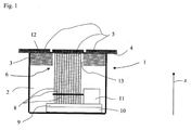
도 1은 주로 EP 2184765로부터 알려진 구성을 갖는 다이 이젝터(1)의 측단면도를 도시한다. 다이 이젝터(1)는 진공압을 공급받을 수 있는 둘러싸인 챔버(2)를 포함하고, 반도체 칩(5)을 갖춘 포일(4)의 일부가 그것 상에 놓이는, 바람직하게는 제거가능하고 교체가능한 커버 플레이트(3)를 포함한다. 챔버(2)는 또한 다이 이젝터(1)의 하우징 또는 그 일부에 의해 형성될 수 있다. 커버 플레이트(3)는 또한 커버일 수 있다. 커버 플레이트(3)는 대략 반도체 칩(5)만큼 큰 직사각형 구멍(6)을 중앙에 포함하고, 바람직하게는 단지 도 2에만 도시되는 그리고 챔버(2)가 진공압을 공급받은 때 포일(4)을 흡인하기 위해 사용되는 복수의 다른 구멍(7)을 포함한다. 다이 이젝터(1)는 또한 챔버(2)의 내부에 서로 나란히 배치되는 그리고 캐리어(9)에 고정되는 복수의 플레이트(8)를 포함한다. 다이 이젝터(1)는 캐리어(9)를 커버 플레이트(3)의 표면(12)에 수직하게, 즉 이 경우 z-방향으로 변위시키기 위해 사용되는 제1 구동 장치(10)를 포함한다. 다이 이젝터(1)는 플레이트(8)를 커버 플레이트(3)의 표면에 수직한 방향으로 캐리어(9)에 대해 변위시키기 위해 사용되는 제2 구동 장치(11)를 포함한다. 따라서, 캐리어(9) 및 플레이트(8) 둘 모두가 포일(4)의 표면에 대해 상승되고 하강될 수 있다.1 shows a cross-sectional side view of a die ejector 1 having a configuration primarily known from EP 2184765. The die ejector 1 comprises an enclosed
플레이트(8)는 커버 플레이트(3)의 중심 구멍(6) 내로 돌출된다. 플레이트(8)와 구멍(6)의 에지 사이에 원주 방향 갭(13)이 있다. 챔버(2)는 진공압을 공급받을 수 있다. 다이 이젝터(1)의 커버 플레이트(3)의 구멍(6) 내에서 플레이트(8)에 의해 점유되는 영역은 바람직하게는 반도체 칩(5)의 영역보다 약간 작으며, 즉 반도체 칩(5)이 모든 측에서 측방향으로 대략 0.5 내지 1 mm만큼 플레이트(8)에 의해 점유되는 영역을 넘어 돌출되도록 치수지어진다. 플레이트(8)의 수 및 형상은 반도체 칩(5)의 치수에 의존한다.The
매우 작은 반도체 칩의 경우에, 즉 전형적으로는 최대 대략 5 mm의 에지 길이를 갖는 반도체 칩(5)의 경우에, 단지 곧은 지지 에지를 갖춘 플레이트(8)만이 사용될 것이다. 중간 크기의 반도체 칩의 경우에, 즉 전형적으로는 대략 5 내지 7 mm 범위의 에지 길이를 갖는 반도체 칩(5)의 경우에, 곧은 지지 에지를 갖춘 플레이트(8)와 L자형 지지 에지를 갖춘 한 쌍의 플레이트가 사용될 것이다. 훨씬 더 큰 반도체 칩(5)의 경우에, 곧은 지지 에지를 갖춘 플레이트(8)와 L자형 지지 에지를 갖춘 두 쌍 이상의(보통 두 쌍의) 플레이트(8)가 사용될 것이다. 곧은 지지 에지를 갖춘 플레이트(8)는 중심에 배치되고, 각각 L자형 지지 에지를 갖춘 플레이트에 의해 쌍을 이루어 둘러싸인다.In the case of very small semiconductor chips, ie typically in the case of
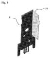
단지 곧은 지지 에지를 갖춘 플레이트(8)만이 명확한 예시를 위해 도 1에 도시된다. 도 3은 L자형 지지 에지(19)를 갖춘 플레이트(8)의 사시도를 도시한다. 지지 에지(19)는 이 실시 형태에서 복수의 치형부를 구비하여, 치형부 사이의 중간 공간 내의 진공압이 포일(4)의 기저부 측에 도달할 것이며, 따라서 흡인력을 증가시킬 것이다. 지지 에지는 또한 치형부 없이, 즉 평평한 에지로서 배치될 수 있다.Only
도 4는 비교적 큰 반도체 칩을 위해 구성된 다이 이젝터(1)의 플레이트(8)의 지지 에지(19)의 평면도를 도시한다. 이 실시 형태의 플레이트는 곧은 지지 에지를 갖춘 9개의 플레이트(8A)와 L자형 지지 에지를 갖춘 두 쌍의 플레이트(8B, 8C), 즉 L자형 지지 에지를 갖춘 총 4개의 플레이트를 포함한다. 용어 "곧은" 및 "L자형"은 지지 평면 내에서 지지 에지(19)의 형상을 지칭한다.4 shows a plan view of the
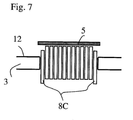
L자형 지지 에지를 갖춘 플레이트(8B)의 제1 쌍(내측 쌍)은 곧은 지지 에지를 갖춘 플레이트(8A)를 둘러싼다. L자형 지지 에지를 갖춘 플레이트(8C)의 제2 쌍(외측 쌍)은 L자형 지지 에지를 갖춘 플레이트(8B)의 내측 쌍을 둘러싼다.The first pair (inner pair) of the
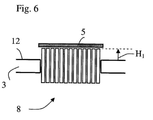
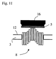
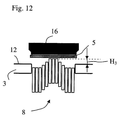
포일(4)로부터 반도체 칩(5)의 탈착 및 제거는 칩 그리퍼(16)(도 10)와 협동하여 다이 이젝터(1)에 의해 행해진다. 칩 그리퍼(16)는 유리하게는 진공압을 공급받을 수 있는 그리고 반도체 칩을 흡인하여 그것을 확고하게 유지시킬 흡인 부재를 포함한다. 칩 그리퍼(16)는 또한 베르누이 효과에 기초하는 흡인 부재를 포함할 수 있으며, 이러한 흡인 부재는 흡인 효과를 달성하기 위해 압축 공기를 공급받을 필요가 있다. 반도체 칩을 탈착하기 위한 방법이 도 5 내지 도 13을 참조하여 상세히 설명될 것이며, 이때 상기 도면은 각각 스냅샷을 나타낸다. 포일(4)과 플레이트(8)의 이동을 위한 구동 수단은 도 5 내지 도 13에 도시되지 않는다. 양의 z-방향으로의 플레이트(8)의 이동이 상승으로 지칭될 것이고, 음의 z-방향으로의 플레이트(8)의 이동이 하강으로 지칭될 것이다.Desorption and removal of the
포일(4)로부터 다음의 반도체 칩을 탈착하기 위해, 탈착될 반도체 칩(5)이 커버 플레이트(3)의 구멍(6) 위에 위치되도록, 포일(4)이 다이 이젝터(1)에 대해 변위된다. 또한, 모든 플레이트(8)가 그 지지 에지(19)가 공통 평면 내에 위치되도록 캐리어(9)에 대해 상승되고, 캐리어(9)는 지지 에지(19)가 커버 플레이트(3)의 표면(12)과 동일 높이에 있는 사전결정된 위치 z0로 이동된다. 이러한 초기 위치에서, 포일(4)이 플레이트(8)의 지지 에지(19) 상에 놓인다. 포일(4)로부터 반도체 칩(5)을 탈착하기 위한 방법은 다음의 단계를 포함한다:In order to detach the next semiconductor chip from the
A) 포일(4)이 커버 플레이트(3)를 향해 끌어당겨지도록 챔버(2)에 진공압을 공급하는 단계;A) supplying vacuum pressure to the
B) 플레이트(8)의 지지 에지(19)가 커버 플레이트(3)의 표면(12) 위로 높이 H1을 취하도록 캐리어(9)를 사전결정된 거리 Δz1만큼 상승시키는 단계;B) raising the
C) L자형 지지 에지를 갖춘 최외측 쌍의 플레이트(8C)를 하강시키는 단계;C) lowering the outermost pair of
D) 선택적으로, L자형 지지 에지를 갖춘 제2 쌍의 플레이트(8B)를 하강시키는 단계;D) optionally, lowering the second pair of
E) 아직 하강되지 않은 플레이트의 지지 에지가 커버 플레이트(3)의 표면(12) 위로 높이 H2 > H1을 취하도록 캐리어(9)를 사전결정된 거리 Δz2만큼 상승시키는 단계;E) raising the
F) 아직 하강되지 않은 플레이트(8)를 사전결정된 순서로 시차를 두고 하강시키는 단계로서, 이때 적어도 하나의 또는 수개의(바람직하게는 3개의) 플레이트(8A)가 하강되지 않는 단계;F) staggering, in a predetermined order, a
G) 선택적으로, 아직 하강되지 않은 플레이트의 지지 에지가 커버 플레이트(3)의 표면(12) 위로 높이 H3 < H2를 취하도록 캐리어(9)를 사전결정된 거리 Δz3만큼 하강시키는 단계;G) optionally, lowering the
H) 아직 하강되지 않은 플레이트(8A)를 시차를 두고 하강시키는 단계;H) staggering the
I) 반도체 칩(5)을 갖춘 칩 그리퍼(16)를 멀리 이동시키는 단계;I) moving the
J) 여기에서 칩 그리퍼(16)는 늦어도 마지막 3개의 플레이트(8A)의 하강 전에 반도체 칩(5) 위에 위치되고 그것이 반도체 칩(5)과 접촉하여 확고하게 유지시킬 때까지 하강된다.J) Here the
도 5는 초기 위치의 스냅샷을 도시한다.5 shows a snapshot of the initial position.
도 6은 단계 B 후의 스냅샷을 도시한다.6 shows a snapshot after step B. FIG.
도 7은 단계 C 후의 스냅샷을 도시한다.7 shows a snapshot after step C.
도 8은 단계 E 후의 스냅샷을 도시한다.8 shows a snapshot after step E. FIG.
도 9 내지 도 11은 단계 E와 G 사이의 연속 스냅샷을 도시한다.9-11 show successive snapshots between steps E and G. FIG.
도 12는 단계 G 후의 스냅샷을 도시한다.12 shows a snapshot after step G.
도 13은 단계 H 후의 스냅샷을 도시한다.13 shows a snapshot after step H. FIG.
각각의 다음의 플레이트의 하강은 도 8 내지 도 12에 도시된 바와 같이 선행하는 플레이트가 완전히 하강되기 전에 행해질 수 있다. 반도체 칩(5)으로부터 포일(4)의 탈착을 위해 칩 그리퍼(16)의 지지가 요구되는 시점은 반도체 칩(5)의 두께, 반도체 칩(5)의 크기, 포일(4)의 접착력, 진공압에 의해 포일(4)에 가해지는 흡인력과 같은 몇몇 요인에 의존한다. 칩 그리퍼(16)가 사용될 필요가 있을 때가 늦어질수록, 자동 조립기의 처리량이 많아진다.The descent of each subsequent plate may be done before the preceding plate is fully lowered as shown in FIGS. 8 to 12. When the
다음의 반도체 칩(5)의 제거를 준비하기 위해, 플레이트(8)가 다시 초기 위치로 이동된다.In order to prepare for removal of the
L자형 지지 에지를 갖춘 플레이트의 사용은 인접 반도체 칩에 대한 기계적 하중의 영향을 감소시키며, 따라서 종래 기술에서보다 큰 높이 H2에 도달하는 것을 허용하고, 이는 포일로부터 반도체 칩의 탈착을 촉진한다.The use of a plate with an L-shaped support edge reduces the influence of mechanical loads on adjacent semiconductor chips, thus allowing to reach a greater height H 2 than in the prior art, which promotes the detachment of the semiconductor chip from the foil.
본 발명의 실시 형태 및 응용이 도시되고 기술되었지만, 본 개시의 이익을 향수하는 당업자에게 전술된 것보다 더욱 많은 변경이 본 명세서의 발명의 개념으로부터 벗어나지 않고서 가능함이 명백할 것이다. 따라서, 본 발명은 첨부 특허청구범위와 그 등가물의 사상을 제외하고는 제한되지 않아야 한다.While embodiments and applications of the present invention have been shown and described, it will be apparent to those skilled in the art having the benefit of this disclosure that many more modifications than those described above are possible without departing from the inventive concepts herein. Accordingly, the invention is not to be restricted except in light of the attached claims and their equivalents.
1: 다이 이젝터 3: 커버 플레이트
4: 포일 5: 반도체 칩
8A, 8B, 8C: 플레이트 9: 캐리어
16: 칩 그리퍼 19: 지지 에지1: die ejector 3: cover plate
4: foil 5: semiconductor chip
8A, 8B, 8C: Plate 9: Carrier
16: chip gripper 19: support edge
Claims (2)
A) 플레이트(8A, 8B, 8C)의 지지 에지(19)가 커버 플레이트(3)의 표면(12) 위로 높이 H1을 취하도록 플레이트(8A, 8B, 8C)를 상승시키는 단계;
B) L자형 지지 에지를 갖춘 제1 쌍의 플레이트(8B)를 하강시키는 단계;
C) 선택적으로, L자형 지지 에지를 갖춘 제2 쌍의 플레이트(8C)를 하강시키는 단계;
D) 아직 하강되지 않은 플레이트의 지지 에지(19)가 커버 플레이트(3)의 표면(12) 위로 높이 H2 > H1을 취하도록, 아직 하강되지 않은 플레이트를 상승시키는 단계;
E) 아직 하강되지 않은 플레이트를 특정 순서로 시차를 두고 하강시키는 단계로서, 적어도 하나의 또는 수개의 플레이트(8A)는 하강되지 않는 단계;
F) 선택적으로, 아직 하강되지 않은 플레이트의 지지 에지(19)가 커버 플레이트(3)의 표면(12) 위로 높이 H3 < H2를 취하도록, 적어도 아직 하강되지 않은 플레이트를 하강시키는 단계;
G) 아직 하강되지 않은 플레이트를 모든 플레이트(8A, 8B, 8C)가 하강될 때까지 하강시키는 단계; 및
H) 반도체 칩(5)을 갖춘 칩 그리퍼(16)를 멀리 이동시키는 단계
를 포함하고,
칩 그리퍼(16)는 늦어도 마지막 3개의 플레이트(8A)의 하강 전에 반도체 칩(5) 위에 위치되고 그것이 반도체 칩(5)과 접촉할 때까지 하강되는 것을 특징으로 하는 방법.As a method for detaching the semiconductor chip 5 from the foil 4 by the chip gripper 16 and the die ejector 1, the die ejector 1 is L-shaped with a first plate 8A having a straight support edge. A second plate 8B, 8C having a supporting edge, wherein the supporting edge 19 of the plates 8A, 8B, 8C forms a support plane on which the foil 4 rests upon it in its initial position. In
A) raising the plates 8A, 8B, 8C so that the support edges 19 of the plates 8A, 8B, 8C take a height H 1 above the surface 12 of the cover plate 3;
B) lowering the first pair of plates 8B having an L-shaped support edge;
C) optionally, lowering the second pair of plates 8C with L-shaped support edges;
D) raising the plate not yet lowered so that the support edge 19 of the plate not yet lowered takes the height H 2 > H 1 above the surface 12 of the cover plate 3;
E) staggering, in a particular order, a plate that has not yet been lowered, wherein at least one or several plates 8A are not lowered;
F) optionally, lowering the at least not yet lowered plate such that the support edge 19 of the plate not yet lowered takes the height H 3 <H 2 over the surface 12 of the cover plate 3;
G) lowering the plate not yet lowered until all the plates 8A, 8B, 8C are lowered; And
H) moving the chip gripper 16 with the semiconductor chip 5 away
Lt; / RTI >
The chip gripper (16) is characterized in that it is positioned at least at the top of the semiconductor chip (5) before the last three plates (8A) and lowered until it contacts the semiconductor chip (5).
플레이트(8A, 8B, 8C)는 캐리어(9)에 고정되며, 캐리어(9)는 커버 플레이트(3)의 표면(12)에 수직하게 변위가능하고, 플레이트(8A, 8B, 8C)는 캐리어(9)에 대해 상승 및 하강될 수 있으며, 캐리어(9)는 초기 위치에서 사전결정된 위치 z0에 배치되고, 플레이트(8A, 8B, 8C)는 캐리어(9)에 대해 상승가능하여, 플레이트(8A, 8B, 8C)의 지지 에지(19)는 포일(4)이 그것 상에 놓이는 지지 평면을 형성하며,
캐리어(9)는 단계 A에서 사전결정된 거리 Δz1만큼 상승되고,
캐리어(9)는 단계 D에서 사전결정된 거리 Δz2만큼 상승되며,
캐리어(9)는 선택적 단계 F에서 사전결정된 거리 Δz3만큼 하강되는 것을 특징으로 하는 방법.The method of claim 1,
The plates 8A, 8B, 8C are fixed to the carrier 9, the carrier 9 is displaceable perpendicular to the surface 12 of the cover plate 3, and the plates 8A, 8B, 8C are mounted on the carrier ( Can be raised and lowered relative to 9), the carrier 9 is disposed at a predetermined position z 0 at the initial position, and the plates 8A, 8B, 8C are ascendable relative to the carrier 9, so that the plate 8A The support edges 19 of 8B, 8C form the support plane on which the foil 4 rests,
The carrier 9 is raised in a step A by a predetermined distance Δz 1 ,
The carrier 9 is raised in a step D by a predetermined distance Δz 2 ,
The carrier (9) is characterized in that the optional step F is lowered by a predetermined distance Δz 3 .
Applications Claiming Priority (2)
| Application Number | Priority Date | Filing Date | Title |
|---|---|---|---|
| CH00453/12A CH706280B1 (en) | 2012-03-30 | 2012-03-30 | A method for detaching a semiconductor chip from a foil. |
| CH453/12 | 2012-03-30 |
Publications (2)
| Publication Number | Publication Date |
|---|---|
| KR20130111366A true KR20130111366A (en) | 2013-10-10 |
| KR102084792B1 KR102084792B1 (en) | 2020-03-04 |
Family
ID=49154876
Family Applications (1)
| Application Number | Title | Priority Date | Filing Date |
|---|---|---|---|
| KR1020130032134A KR102084792B1 (en) | 2012-03-30 | 2013-03-26 | Method for detaching a semiconductor chip from a foil |
Country Status (10)
| Country | Link |
|---|---|
| US (1) | US9039867B2 (en) |
| JP (1) | JP6128459B2 (en) |
| KR (1) | KR102084792B1 (en) |
| CN (1) | CN103367136B (en) |
| CH (1) | CH706280B1 (en) |
| DE (1) | DE102013103100B4 (en) |
| FR (1) | FR2988902B1 (en) |
| MY (1) | MY164119A (en) |
| SG (1) | SG193709A1 (en) |
| TW (1) | TWI569338B (en) |
Cited By (4)
| Publication number | Priority date | Publication date | Assignee | Title |
|---|---|---|---|---|
| KR20170029511A (en) * | 2014-06-18 | 2017-03-15 | 매뉴팩쳐링 인테그레이션 테크놀로지 리미티드 | System and method for peeling a semiconductor chip from a tape using a multistage ejector |
| KR102020034B1 (en) * | 2019-07-09 | 2019-09-10 | (주)삼정오토메이션 | Multi-layer ceramic capacitor extraction method |
| KR20200034600A (en) * | 2018-09-21 | 2020-03-31 | 파스포드 테크놀로지 주식회사 | Semiconductor manufacturing apparatus, push-up jig and method for manufacturing semiconductor device |
| KR102177863B1 (en) * | 2020-08-07 | 2020-11-11 | 변영기 | Apparatus for peeling off film on chip |
Families Citing this family (11)
| Publication number | Priority date | Publication date | Assignee | Title |
|---|---|---|---|---|
| CH707236B1 (en) | 2012-11-23 | 2016-10-31 | Besi Switzerland Ag | A method for detaching semiconductor chips from a film. |
| JP5717910B1 (en) * | 2014-02-26 | 2015-05-13 | 株式会社新川 | Semiconductor die pickup apparatus and pickup method |
| JP6797569B2 (en) * | 2016-06-13 | 2020-12-09 | ファスフォードテクノロジ株式会社 | Semiconductor manufacturing equipment and manufacturing method of semiconductor equipment |
| TWI648213B (en) * | 2017-11-30 | 2019-01-21 | 景碩科技股份有限公司 | Tear foil mechanism |
| JP2019169516A (en) * | 2018-03-22 | 2019-10-03 | 東芝メモリ株式会社 | Thrusting-up device and thrusting-up method for semiconductor device |
| CN109192681B (en) * | 2018-09-01 | 2022-05-31 | 佛山市美特智能科技有限公司 | Rapid flexible manufacturing system of chip |
| CH715447B1 (en) | 2018-10-15 | 2022-01-14 | Besi Switzerland Ag | chip ejector. |
| DE102018125682B4 (en) * | 2018-10-16 | 2023-01-19 | Asm Assembly Systems Gmbh & Co. Kg | Ejector device and method for assisting detachment of an electrical component arranged on a holding film |
| US11764098B2 (en) * | 2021-04-16 | 2023-09-19 | Asmpt Singapore Pte. Ltd. | Detaching a die from an adhesive tape by air ejection |
| JP2023064405A (en) * | 2021-10-26 | 2023-05-11 | 三菱電機株式会社 | Semiconductor manufacturing device and method for manufacturing semiconductor device |
| JP2023167124A (en) | 2022-05-11 | 2023-11-24 | 三星電子株式会社 | Chip peeling device and chip peeling method |
Citations (4)
| Publication number | Priority date | Publication date | Assignee | Title |
|---|---|---|---|---|
| KR20050028802A (en) * | 2003-09-17 | 2005-03-23 | 가부시끼가이샤 르네사스 테크놀로지 | Method of manufacturing semiconductor device |
| KR20100050432A (en) * | 2008-11-05 | 2010-05-13 | 에섹 에스에이 | Die ejector |
| KR20100110274A (en) * | 2009-04-02 | 2010-10-12 | 에이에스엠 어쌤블리 오토메이션 리미티드 | Device for thin die detachment and pick-up |
| KR20110091469A (en) * | 2010-02-05 | 2011-08-11 | 에이에스엠 어쌤블리 오토메이션 리미티드 | Control and monitoring system for thin die detachment and pick-up |
Family Cites Families (9)
| Publication number | Priority date | Publication date | Assignee | Title |
|---|---|---|---|---|
| JP3976541B2 (en) | 2001-10-23 | 2007-09-19 | 富士通株式会社 | Semiconductor chip peeling method and apparatus |
| CH697213A5 (en) * | 2004-05-19 | 2008-06-25 | Alphasem Ag | Method and apparatus for peeling a film adhered to a flexible component. |
| JP4735829B2 (en) * | 2005-12-06 | 2011-07-27 | 澁谷工業株式会社 | Chip push-up device |
| US7665204B2 (en) * | 2006-10-16 | 2010-02-23 | Asm Assembly Automation Ltd. | Die detachment apparatus comprising pre-peeling structure |
| JP4693805B2 (en) * | 2007-03-16 | 2011-06-01 | 株式会社東芝 | Semiconductor device manufacturing apparatus and manufacturing method |
| TWI463580B (en) | 2007-06-19 | 2014-12-01 | Renesas Electronics Corp | Manufacturing method of semiconductor integrated circuit device |
| JP4864816B2 (en) * | 2007-06-19 | 2012-02-01 | ルネサスエレクトロニクス株式会社 | Manufacturing method of semiconductor integrated circuit device |
| JP2011216529A (en) * | 2010-03-31 | 2011-10-27 | Furukawa Electric Co Ltd:The | Method for manufacturing semiconductor device |
| CH707236B1 (en) * | 2012-11-23 | 2016-10-31 | Besi Switzerland Ag | A method for detaching semiconductor chips from a film. |
-
2012
- 2012-03-30 CH CH00453/12A patent/CH706280B1/en not_active IP Right Cessation
-
2013
- 2013-02-26 SG SG2013014311A patent/SG193709A1/en unknown
- 2013-02-28 FR FR1351764A patent/FR2988902B1/en active Active
- 2013-03-15 US US13/839,586 patent/US9039867B2/en active Active
- 2013-03-15 JP JP2013053218A patent/JP6128459B2/en active Active
- 2013-03-22 MY MYPI2013001000A patent/MY164119A/en unknown
- 2013-03-22 CN CN201310113448.XA patent/CN103367136B/en active Active
- 2013-03-26 KR KR1020130032134A patent/KR102084792B1/en active IP Right Grant
- 2013-03-26 DE DE102013103100.5A patent/DE102013103100B4/en active Active
- 2013-03-28 TW TW102111159A patent/TWI569338B/en active
Patent Citations (4)
| Publication number | Priority date | Publication date | Assignee | Title |
|---|---|---|---|---|
| KR20050028802A (en) * | 2003-09-17 | 2005-03-23 | 가부시끼가이샤 르네사스 테크놀로지 | Method of manufacturing semiconductor device |
| KR20100050432A (en) * | 2008-11-05 | 2010-05-13 | 에섹 에스에이 | Die ejector |
| KR20100110274A (en) * | 2009-04-02 | 2010-10-12 | 에이에스엠 어쌤블리 오토메이션 리미티드 | Device for thin die detachment and pick-up |
| KR20110091469A (en) * | 2010-02-05 | 2011-08-11 | 에이에스엠 어쌤블리 오토메이션 리미티드 | Control and monitoring system for thin die detachment and pick-up |
Cited By (4)
| Publication number | Priority date | Publication date | Assignee | Title |
|---|---|---|---|---|
| KR20170029511A (en) * | 2014-06-18 | 2017-03-15 | 매뉴팩쳐링 인테그레이션 테크놀로지 리미티드 | System and method for peeling a semiconductor chip from a tape using a multistage ejector |
| KR20200034600A (en) * | 2018-09-21 | 2020-03-31 | 파스포드 테크놀로지 주식회사 | Semiconductor manufacturing apparatus, push-up jig and method for manufacturing semiconductor device |
| KR102020034B1 (en) * | 2019-07-09 | 2019-09-10 | (주)삼정오토메이션 | Multi-layer ceramic capacitor extraction method |
| KR102177863B1 (en) * | 2020-08-07 | 2020-11-11 | 변영기 | Apparatus for peeling off film on chip |
Also Published As
| Publication number | Publication date |
|---|---|
| CH706280B1 (en) | 2016-03-15 |
| DE102013103100A1 (en) | 2013-10-02 |
| TWI569338B (en) | 2017-02-01 |
| JP6128459B2 (en) | 2017-05-17 |
| JP2013214739A (en) | 2013-10-17 |
| CH706280A1 (en) | 2013-09-30 |
| TW201401384A (en) | 2014-01-01 |
| FR2988902A1 (en) | 2013-10-04 |
| KR102084792B1 (en) | 2020-03-04 |
| US9039867B2 (en) | 2015-05-26 |
| MY164119A (en) | 2017-11-30 |
| SG193709A1 (en) | 2013-10-30 |
| CN103367136B (en) | 2017-08-25 |
| FR2988902B1 (en) | 2016-12-30 |
| US20130255889A1 (en) | 2013-10-03 |
| CN103367136A (en) | 2013-10-23 |
| DE102013103100B4 (en) | 2024-02-29 |
Similar Documents
| Publication | Publication Date | Title |
|---|---|---|
| KR102084792B1 (en) | Method for detaching a semiconductor chip from a foil | |
| KR101612034B1 (en) | Die ejector | |
| KR101596461B1 (en) | Apparatus and Method for Chip Detaching | |
| KR101627906B1 (en) | Apparatus for ejecting a die | |
| JP5445534B2 (en) | Electronic component mounting apparatus, electronic component mounting method, and layout changing method of receiving pin module | |
| WO2013021593A1 (en) | Bottom reception pin module for electronic component mounting device, substrate bottom reception device, and substrate bottom reception method | |
| KR100865766B1 (en) | Semiconductor die ejecting apparatus | |
| JP7241786B2 (en) | Semiconductor chip pickup device, semiconductor chip mounting device and mounting method | |
| KR20160068201A (en) | Apparatus for ejecting a die | |
| JP2020074397A (en) | Pick-up apparatus and implementation apparatus for semiconductor chip | |
| TW202025275A (en) | Die ejecting apparatus | |
| JP6019406B2 (en) | Electronic component mounting apparatus and electronic component mounting method | |
| JP2010087359A (en) | Pickup apparatus | |
| KR101688989B1 (en) | Ic separation equipment | |
| CN102024730B (en) | Placing mechanism, transport method of wafer having dicing frame | |
| JP4816622B2 (en) | Chip peeling device, chip peeling method, and chip pickup device | |
| KR101344367B1 (en) | Die ejecting apparatus | |
| JP2019123035A (en) | Holding table | |
| KR20110050027A (en) | Pick-up apparatus of semiconductor die | |
| KR20090053682A (en) | Equipment for die pick up and method for detatching of semiconductor chip using the same | |
| TWI717775B (en) | Needle device for die | |
| CN108878339B (en) | Disengaging device | |
| KR20220097092A (en) | Die transfer module and die bonding apparatus including the same | |
| KR101675915B1 (en) | an apparatus for separating and picking up a semiconductor device using multi pick and place including guiding means, and a method using it. | |
| JP2014225593A (en) | Electronic component mounting apparatus and electronic component mounting method |
Legal Events
| Date | Code | Title | Description |
|---|---|---|---|
| A201 | Request for examination | ||
| E902 | Notification of reason for refusal | ||
| E701 | Decision to grant or registration of patent right | ||
| GRNT | Written decision to grant |