KR20130100325A - Systems and methods for forming a layer of sputtered material - Google Patents
Systems and methods for forming a layer of sputtered material Download PDFInfo
- Publication number
- KR20130100325A KR20130100325A KR1020137011057A KR20137011057A KR20130100325A KR 20130100325 A KR20130100325 A KR 20130100325A KR 1020137011057 A KR1020137011057 A KR 1020137011057A KR 20137011057 A KR20137011057 A KR 20137011057A KR 20130100325 A KR20130100325 A KR 20130100325A
- Authority
- KR
- South Korea
- Prior art keywords
- substrate
- target
- relative position
- coating
- rotatable
- Prior art date
Links
Images


Classifications
-
- C—CHEMISTRY; METALLURGY
- C23—COATING METALLIC MATERIAL; COATING MATERIAL WITH METALLIC MATERIAL; CHEMICAL SURFACE TREATMENT; DIFFUSION TREATMENT OF METALLIC MATERIAL; COATING BY VACUUM EVAPORATION, BY SPUTTERING, BY ION IMPLANTATION OR BY CHEMICAL VAPOUR DEPOSITION, IN GENERAL; INHIBITING CORROSION OF METALLIC MATERIAL OR INCRUSTATION IN GENERAL
- C23C—COATING METALLIC MATERIAL; COATING MATERIAL WITH METALLIC MATERIAL; SURFACE TREATMENT OF METALLIC MATERIAL BY DIFFUSION INTO THE SURFACE, BY CHEMICAL CONVERSION OR SUBSTITUTION; COATING BY VACUUM EVAPORATION, BY SPUTTERING, BY ION IMPLANTATION OR BY CHEMICAL VAPOUR DEPOSITION, IN GENERAL
- C23C14/00—Coating by vacuum evaporation, by sputtering or by ion implantation of the coating forming material
- C23C14/22—Coating by vacuum evaporation, by sputtering or by ion implantation of the coating forming material characterised by the process of coating
- C23C14/34—Sputtering
- C23C14/35—Sputtering by application of a magnetic field, e.g. magnetron sputtering
- C23C14/352—Sputtering by application of a magnetic field, e.g. magnetron sputtering using more than one target
-
- H—ELECTRICITY
- H01—ELECTRIC ELEMENTS
- H01J—ELECTRIC DISCHARGE TUBES OR DISCHARGE LAMPS
- H01J37/00—Discharge tubes with provision for introducing objects or material to be exposed to the discharge, e.g. for the purpose of examination or processing thereof
- H01J37/32—Gas-filled discharge tubes
- H01J37/34—Gas-filled discharge tubes operating with cathodic sputtering
- H01J37/3402—Gas-filled discharge tubes operating with cathodic sputtering using supplementary magnetic fields
- H01J37/3405—Magnetron sputtering
-
- H—ELECTRICITY
- H01—ELECTRIC ELEMENTS
- H01J—ELECTRIC DISCHARGE TUBES OR DISCHARGE LAMPS
- H01J37/00—Discharge tubes with provision for introducing objects or material to be exposed to the discharge, e.g. for the purpose of examination or processing thereof
- H01J37/32—Gas-filled discharge tubes
- H01J37/34—Gas-filled discharge tubes operating with cathodic sputtering
- H01J37/3464—Operating strategies
- H01J37/3473—Composition uniformity or desired gradient
Abstract
본 발명은 기판(110)을 코팅하는 방법을 설명하며, 상기 방법은 기판(110) 상에 스퍼터링된 물질의 층(806)을 형성하는 단계를 포함한다. 스퍼터링된 물질의 층을 형성하는 단계는 기판(110)에 걸쳐 적어도 하나의 회전가능한 타겟(120')으로부터 물질을 스퍼터링하는 단계; 적어도 하나의 타겟(120')과 기판(110) 사이의 상대적인 위치를 변경하는 단계를 포함할 수 있다. 게다가, 본 발명은 타겟(120; 120'; 120")과 기판 사의의 거리를 스퍼터 프로세스 동안 변경하는 것을 설명한다. 본 발명은 기판을 코팅하기 위한 시스템을 더 설명한다. The present invention describes a method of coating a substrate 110, which method includes forming a layer 806 of sputtered material on the substrate 110. Forming a layer of sputtered material includes sputtering material from at least one rotatable target 120 ′ across the substrate 110; The method may include changing a relative position between the at least one target 120 ′ and the substrate 110. In addition, the present invention describes changing the distance between the target 120 (120 '; 120 ") and the substrate yarn during the sputter process. The present invention further describes a system for coating a substrate.
Description
본 발명의 실시예들은 기판 상에 층을 코팅하기 위한 시스템들 및 방법들에 관한 것으로, 특히, 기판 상에 스퍼터링된 물질의 층을 형성하는 방법들 및 시스템들에 관한 것이다. 더 명확하게는, 본 발명의 적어도 일부 양상들은 마그네트론 스퍼터링에 관한 것이고, 여기서, 타겟은, 예를 들면, 회전가능한 원통형 타겟 또는 평면 타겟일 수 있지만, 이에 제한되지 않는다. 더욱 더 명확하게는, 본 발명의 일부 양상들은 정적 스퍼터링 증착에 관한 것이다. 본 발명의 적어도 일부 양상들은 특히, 반도체 및 유전 물질들 및 디바이스들, 실리콘-기반 웨이퍼들, 평판 디스플레이들(TFT들과 같은), 마스크들 및 필터들, 에너지 변환 및 스토리지(광 전지들, 연료 전지들, 및 배터리들과 같은), 고체 조명(LED들 및 OLED들과 같은), 자기 및 광학 스토리지, 마이크로-전자-기계 시스템들(MEMS) 및 나노-전자-기계 시스템들(NEMS), 마이크로-광학 및 광전 디바이스들, 투명 기판들, 건축 및 자동차 유리들, 금속 및 폴리머 포일들(foil) 및 패키징을 위한 금속화 시스템들, 및 마이크로- 및 나노-몰딩 성형을 포함하는 애플리케이션들을 포함하지만, 이에 제한되지 않는 대표적인 예들 갖는 증착, 패터닝, 및 기판들의 처리 및 코팅들에 사용되는 장비, 프로세스들 및 물질들을 수반하는 기판 코팅 기술 해결책들에 관한 것이다. Embodiments of the present invention relate to systems and methods for coating a layer on a substrate, and more particularly to methods and systems for forming a layer of sputtered material on a substrate. More specifically, at least some aspects of the present invention relate to magnetron sputtering, where the target may be, for example, a rotatable cylindrical target or a planar target, but is not limited thereto. Even more clearly, some aspects of the present invention relate to static sputter deposition. At least some aspects of the present invention, in particular, include semiconductor and dielectric materials and devices, silicon-based wafers, flat panel displays (such as TFTs), masks and filters, energy conversion and storage (photovoltaic cells, fuel) Cells, and batteries), solid state lighting (such as LEDs and OLEDs), magnetic and optical storage, micro-electro-mechanical systems (MEMS) and nano-electro-mechanical systems (NEMS), micro Applications include optical and optoelectronic devices, transparent substrates, architectural and automotive glass, metallization systems for metal and polymer foils and packaging, and micro- and nano-molding molding, Representative examples include, but are not limited to, substrate coating technology solutions involving equipment, processes, and materials used in deposition, patterning, and processing and coatings of substrates.
고 균일성으로(즉, 넓은 표면에 걸친 균일한 두께) 기판 상에 층을 형성하는 것은 많은 기술 분야에서 중요한 문제이다. 예를 들면, 막박 트랜지스터들(TFT)의 분야에서, 두께 균일성은 디스플레이 금속 라인들을 신뢰성 있게 제조하기 위한 비결일 수 있다. 게다가, 균일한 층은 일반적으로 제조 재현성을 용이하게 한다. Forming a layer on a substrate with high uniformity (ie, uniform thickness across a large surface) is an important issue in many technical fields. For example, in the field of thin film transistors (TFTs), thickness uniformity may be the key to reliably fabricating display metal lines. In addition, uniform layers generally facilitate manufacturing reproducibility.
기판 상에 층을 형성하기 위한 하나의 방법은 스퍼터링인데, 이는 다양한 제조 분야들에서, 예를 들면, TFT들의 제조에서 가치가 큰 방법으로서 개발되어왔다 . 스퍼터링 동안, 원자들은 강력한 입자들(예를 들면, 불활성 또는 반응성 가스의 에너지화된 이온들)과의 충격에 의해 타겟 물질로부터 방출된다. 그에 의해, 방출된 원자들은 기판 상에 증착될 수 있고, 그래서 스퍼터링된 물질의 층이 형성될 수 있다. One method for forming a layer on a substrate is sputtering, which has been developed as a valuable method in various manufacturing fields, for example in the manufacture of TFTs. During sputtering, atoms are released from the target material by impact with powerful particles (eg, energized ions of an inert or reactive gas). Thereby the released atoms can be deposited on the substrate, so that a layer of sputtered material can be formed.
그러나, 스퍼터링에 의한 층의 형성은, 예를 들면, 타겟 및/또는 기판의 기하형상에 기인하여 고 균일성 요구조건들을 위태롭게 할 수 있다. 특히, 대규모 기판들에 걸친 스퍼터링된 물질의 균일한 층들은 스퍼터링된 물질의 불규칙한 공간 분포에 기인하여 달성하기 곤란할 수 있다. 기판에 걸친 복수의 타겟들의 공급은 층 균일성을 개선시킬 수 있다. 다른 선택은 마그네트론 스퍼터 캐소드의 자석을 어떤 외곽 위치들과 영점(zero-position) 부근 사이에 일정한 각속도로 회전시키는 것이다. 그러나, 특히, 층 균일성에 관한 높은 요구조건들을 제기하는 일부 애플리케이션들에 대해, 그에 의해 달성된 층 균일성은 충분하지 않을 수 있다. However, formation of a layer by sputtering may jeopardize high uniformity requirements, for example, due to the geometry of the target and / or substrate. In particular, uniform layers of sputtered material over large substrates may be difficult to achieve due to the irregular spatial distribution of the sputtered material. Supply of a plurality of targets across the substrate can improve layer uniformity. Another option is to rotate the magnet of the magnetron sputter cathode at a constant angular velocity between some outer positions and near zero-position. However, especially for some applications that pose high requirements regarding layer uniformity, the layer uniformity achieved thereby may not be sufficient.
따라서, 스퍼터링된 물질의 매우 균일한 층을 용이하게 하기 위한 추가 방법들 및/또는 시스템들이 요구된다. Thus, additional methods and / or systems are needed to facilitate a very uniform layer of sputtered material.
일 양상에서, 기판을 코팅하는 방법이 제공된다. 상기 방법은 기판 상에 스퍼터링된 물질의 층을 형성하는 단계를 포함하고, 스퍼터링된 물질의 층을 형성하는 단계는 기판에 걸쳐 하나 또는 둘 이상의 회전가능한 타겟들로부터 물질을 스퍼터링하는 단계를 포함한다. 상기 방법은 하나 또는 둘 이상의 회전가능한 타겟들과 기판 사이의 상대적인 위치를 변경하는(varying) 단계를 포함한다. In one aspect, a method of coating a substrate is provided. The method includes forming a layer of sputtered material on a substrate, and forming the layer of sputtered material includes sputtering material from one or more rotatable targets over the substrate. The method includes varying the relative position between one or more rotatable targets and the substrate.
다른 양상에서, 기판을 코팅하기 위한 방법이 제공된다. 상기 방법은 기판 상에 스퍼터링된 물질의 층을 형성하는 단계를 포함하고, 형성 단계는 기판에 걸쳐 하나 또는 둘 이상의 타겟들로부터 물질을 스퍼터링하는 단계 및 하나 또는 둘 이상의 타겟들과 기판 사이의 거리를 변경함으로써 하나 또는 둘 이상의 타겟들과 기판 사이의 상대적인 위치를 변경하는 단계를 포함한다. In another aspect, a method for coating a substrate is provided. The method includes forming a layer of sputtered material on a substrate, the forming step comprising sputtering the material from one or more targets across the substrate and determining a distance between the one or more targets and the substrate. Altering the relative position between the one or more targets and the substrate.
또 다른 양상에서, 기판을 코팅하는 방법이 제공되고, 이 방법은 기판 상에 스퍼터링된 물질의 층을 형성하는 단계를 포함한다. 스퍼터링된 물질의 층을 형성하는 단계는 기판에 걸쳐 하나 또는 둘 이상의 타겟으로부터 물질을 스퍼터링하는 단계; 하나 또는 둘 이상의 타겟들과 기판 사이의 상대적인 위치를 제 1 위치로 변경하는 단계 - 제 1 위치는 미리 결정된 제 1 시간 간격 동안 유지됨 - ; 및 하나 또는 둘 이상의 타겟들과 기판 사이의 상대적인 위치를 제 2 위치로 변경하는 단계 - 제 2 위치는 미리 결정된 제 2 시간 간격 동안 유지됨 -를 포함한다. In another aspect, a method of coating a substrate is provided, the method comprising forming a layer of sputtered material on the substrate. Forming a layer of sputtered material includes sputtering material from one or more targets across the substrate; Changing a relative position between one or more targets and the substrate to a first position, wherein the first position is maintained for a first predetermined time interval; And changing the relative position between the one or more targets and the substrate to a second position, wherein the second position is maintained for a second predetermined time interval.
다른 양상에서, 기판을 코팅하기 위한 다른 방법이 제공되며, 이 방법은 기판 상에 스퍼터링된 물질의 층을 형성하는 단계를 포함한다. 스퍼터링된 물질의 층을 형성하는 단계는 기판에 걸쳐 하나 또는 둘 이상의 타겟들로부터 물질을 스퍼터링하는 단계 - 하나 또는 둘 이상의 타겟들은 평면 타겟임 - ; 및 왕복 방식으로 하나 또는 둘 이상의 타겟들을 회전시킴으로써 하나 또는 둘 이상의 타겟들과 기판 사이의 상대적인 위치를 변경하는 단계를 포함한다. In another aspect, another method is provided for coating a substrate, the method comprising forming a layer of sputtered material on the substrate. Forming a layer of sputtered material comprises sputtering material from one or more targets across the substrate, wherein the one or more targets are planar targets; And changing the relative position between the one or more targets and the substrate by rotating the one or more targets in a reciprocating manner.
또 다른 양상에서, 기판을 코팅하기 위한 시스템이 제공된다. 상기 시스템은 상기 기판 상에 물질을 스퍼터링하기 위한 하나 또는 둘 이상의 회전가능한 타겟들을 포함하고, 하나 또는 둘 이상의 회전가능한 타겟들은 상기 기판의 코팅 동안 하나 또는 둘 이상의 회전가능한 타겟들과 기판 사이의 상대적인 위치가 변경되는 방식으로 이동되도록 구성된다. In another aspect, a system for coating a substrate is provided. The system includes one or more rotatable targets for sputtering material on the substrate, wherein the one or more rotatable targets are positioned relative to the substrate and the one or more rotatable targets during coating of the substrate. It is configured to be moved in a way that is changed.
또 다른 양상에서, 기판을 코팅하기 위한 시스템이 제공된다. 상기 시스템은 상기 기판 상에 물질을 스퍼터링하기 위한 하나 또는 둘 이상의 타겟들을 포함하고, 하나 또는 둘 이상의 타겟들은 상기 기판의 코팅 동안 하나 또는 둘 이상의 타겟들과 기판 사이의 거리가 변경되는 방식으로 이동되도록 구성된다. In another aspect, a system for coating a substrate is provided. The system includes one or more targets for sputtering material on the substrate, wherein the one or more targets are moved in such a way that the distance between the one or more targets and the substrate changes during coating of the substrate. It is composed.
또 다른 양상에서, 기판을 코팅하기 위한 시스템이 제공된다. 상기 시스템은 기판 상에 물질을 스퍼터링하기 위한 하나 또는 둘 이상의 평면 타겟들을 포함한다. 하나 또는 둘 이상의 평면 타겟들은 기판의 코팅 동안 하나 또는 둘 이상의 타겟들과 기판 사이의 상대적인 위치가 변경되는 방식으로 왕복 방식으로 회전가능하다. In another aspect, a system for coating a substrate is provided. The system includes one or more planar targets for sputtering material on a substrate. One or more planar targets are rotatable in a reciprocating manner such that the relative position between the one or more targets and the substrate is changed during coating of the substrate.
본 발명의 추가 양상들, 장점들 및 특징들은 종속된 청구범위, 상세한 설명 및 첨부된 도면들로부터 명백하다. Further aspects, advantages and features of the invention are apparent from the dependent claims, the description and the accompanying drawings.
그의 최적 방식(best mode)을 포함하며, 당업자에 대해 완전하고 합법화하는 발명은 첨부된 도면들에 대한 참조를 포함하는 명세서의 암시로 더 특별하게 설명된다.
도 1, 도 2, 도 3; 도 5 내지 도 7; 및 도 11 내지 도 19는 본 명세서에서 설명된 실시예들에 따른 기판을 코팅하기 위한 예시적인 시스템들의 개략도들이고;
도 4 및 도 10은 본 명세서에서 설명된 실시예들에 따른 캐소드 조립체에 인가되는 전압 파형의 개략적인 다이어그램들이며; 및
도 8 및 도 9는 본 명세서에서의 실시예들에 따른 스퍼터링된 물질의 층의 형성을 도시하는 정성(qualitative) 다이어그램들이다. The invention, including its best mode, which is fully and legitimate for a person of ordinary skill in the art, is more particularly described by the implications of the specification including references to the accompanying drawings.
1, 2, and 3; 5 to 7; 11-19 are schematic diagrams of example systems for coating a substrate in accordance with embodiments described herein;
4 and 10 are schematic diagrams of voltage waveforms applied to a cathode assembly in accordance with embodiments described herein; And
8 and 9 are qualitative diagrams illustrating the formation of a layer of sputtered material in accordance with embodiments herein.
참조는 이제 다양한 실시예들에 대하여 상세하게 이루어질 것이고, 이들의 하나 또는 둘 이상의 예들은 각각의 도면에 도시된다. 각각의 예는 설명에 의해 제공되고, 제한으로서 의미되지 않는다. 예를 들면, 일 실시예의 일부로서 도시되거나 설명된 특징들은 더 추가적인 실시예들을 산출하기 위해 다른 실시예에 또는 다른 실시예들과 함께 사용될 수 있다. 본 발명이 이러한 수정예들 및 변형예들을 포함함이 의도된다. Reference will now be made in detail to various embodiments, one or more examples of which are shown in each figure. Each example is provided by way of explanation and is not meant as a limitation. For example, features shown or described as part of one embodiment may be used in other embodiments or in conjunction with other embodiments to yield further embodiments. It is intended that the present invention include such modifications and variations.
본 명세서에서 설명된 실시예들은 층을 갖는 기판을 코팅하기 위한 방법들 및 시스템들을 포함하고, 이 층에서 층을 형성하기 위한 프로세스 동안, 기판에 걸쳐 스퍼터링된 물질의 분포가 변경된다. 특히, 본 명세서에서 설명된 실시예들은 타겟과 기판 사이의 상대적인 위치(또한 타겟-기판 상대적인 위치로 지칭됨)를 변경하는 단계를 포함한다. 일반적으로, 이러한 상대적인 위치는, 아래에 더 논의된 바와 같이, 적어도 2개의 별개의 위치들(이하에서 제 1 위치 및 제 2 위치로 지칭됨)에서 미리 결정된 시간 간격 동안 유지된다. Embodiments described herein include methods and systems for coating a substrate having a layer, during which the distribution of sputtered material across the substrate is changed during the process for forming the layer in the layer. In particular, the embodiments described herein include changing the relative position (also referred to as the target-substrate relative position) between the target and the substrate. In general, this relative position is maintained for a predetermined time interval at at least two separate positions (hereinafter referred to as first position and second position), as further discussed below.
적어도 일부 다른 실시예들은, 아래에 더 논의된 바와 같이, 왕복 방식으로 특히, 평면 타겟을, 더 특별히 그의 세로축에 대해, 또는 그에 결합된 평면 캐소드 조립체를 회전하는 단계를 포함한다. 본 명세서에서 사용된 바와 같은 용어 왕복은 앞-뒤로의 운동을 지칭한다. 본 명세서에서 설명된 실시예들에 따르면, 회전가능한 타겟 또는 회전가능한 타겟들의 어레이는 왕복 방식으로 이동된다. At least some other embodiments include rotating the planar target assembly, in particular in a reciprocating manner, more particularly about its longitudinal axis, or coupled thereto, in a reciprocating manner, as discussed further below. The term reciprocal, as used herein, refers to forward-backward movement. According to the embodiments described herein, the rotatable target or the array of rotatable targets is moved in a reciprocating manner.
어떤 실시예들에 따르면, 적어도 하나의 타겟으로부터 물질을 스퍼터링하는 단계는, 아래에 더 논의된 바와 같이, 2개의 실질적인 상호보완적인 막 분포들을 중첩하는 단계를 포함한다. 본 발명 내에서 용어 "실질적으로"는 가까운, 접근하는, 또는 정확하게 어떤 상태 또는 값, 나타내는 것으로, 예를 들면, 20%, 더 명확하게는 10%, 더 명확하게는 5%보다 작은 편차를 포함하는 것으로 이해될 것이다. According to some embodiments, sputtering the material from at least one target includes superimposing two substantially complementary membrane distributions, as discussed further below. The term "substantially" within the present invention refers to any state or value that is close, approaching, or exactly, including, for example, a deviation of less than 20%, more specifically 10%, more specifically 5%. Will be understood.
그에 의해, 본 발명의 실시예들은 기판 상의 층들의 형성을 용이하게 하고, 층들은 고 품질을 갖는다. 특히, 기판 상에 증착된 층의 두께는 전체 기판에 걸쳐 매우 균일할 수 있다. 게다가, 그에 의해, 층의 고 동질성(homogeneity)이 용이하게 된다(예를 들면, 성장 결정체의 구조, 특정한 저항, 및/또는 층 응력과 같은 특성들의 면에서). 예를 들면, 본 발명의 실시예들은, 그 안에서, 신호 지연이 층의 두께에 의존하고, 그래서 두께 비-균일성이 매우 상이한 시간들에서 동력이 공급되는(energize) 화소들을 초래할 수 있기 때문에, TFT들의 생산에서(예를 들면, TFT-LCD 디스플레이들의 제조를 위한) 금속화된 층들을 형성하는데 유리할 수 있다. 게다가, 본 발명의 실시예들은 층 두께의 균일성이 형성된 층의 상이한 위치들에서 동일한 결과를 달성하는 것을 용이하게 하기 때문에, 나중에 식각되는 층을 형성하는데 유리할 수 있다. Thereby, embodiments of the present invention facilitate the formation of layers on the substrate, and the layers have high quality. In particular, the thickness of the layer deposited on the substrate can be very uniform over the entire substrate. In addition, the homogeneity of the layer is thereby facilitated (eg in terms of properties such as structure of the growth crystals, specific resistance, and / or layer stress). For example, embodiments of the present invention, because signal delay therein depends on the thickness of the layer, so that thickness non-uniformity can result in energized pixels at very different times, It may be advantageous to form metallized layers in the production of TFTs (eg for the manufacture of TFT-LCD displays). In addition, embodiments of the present invention may be advantageous for forming a layer to be etched later, since the uniformity of the layer thickness facilitates achieving the same result at different positions of the formed layer.
도면들의 다음 설명 내에서, 동일한 참조 부호들은 동일한 컴포넌트를 지칭한다. 일반적으로, 개별 실시예들에 대한 차이점만이 설명된다. Within the following description of the drawings, like reference numerals refer to like components. In general, only the differences for the individual embodiments are described.
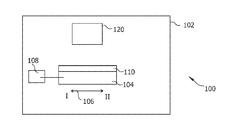
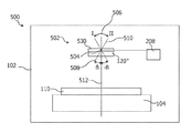
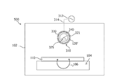
도 1은 기판(110)을 코팅하기 위한 시스템(100)의 개략도이다. 본 명세서에 설명된 바와 같이, 스퍼터링된 물질로 기판을 코팅하는 프로세스는 일반적으로 막-박 애플리케이션들로 지칭된다. 용어 "코팅" 및 용어 "증착"은 본 명세서에서 동의어로 사용된다. 본 명세서에서 사용된 바와 같은 용어 "기판"은 구부러지지 않는 기판들(예를 들면, 웨이퍼 또는 유리 판이지만, 이에 제한되지 않음) 및 구부러지기 쉬운 기판들(예를 들면, 웹(web) 또는 포일(foil)이지만, 이에 제한되지 않음) 모두를 포괄할 것이다. 1 is a schematic diagram of a
도 1의 예시적인 코팅 시스템은 기판(110) 위에 배치되는 타겟(120)을 포함하고, 그래서 타겟(120)으로부터 스퍼터링된 물질은 기판(110) 상에 증착할 수 있다. 본 명세서에서 사용된 바와 같은 용어 "타겟"은 그의 스퍼터링에 의해 기판에 걸쳐 층을 형성하기 위한 소스 물질을 포함하는 고체 바디를 지칭한다. 일반적인 실시예들에 따르면, 타겟(120)은 실질적으로 원통형으로 형성된다. 대안적으로, 타겟(120)은 코팅 시스템(100)이 본 명세서에서 설명된 바와 같이 층을 형성할 수 있는 임의의 기하형성을 가질 수 있다. 게다가, 타겟(120)은 도 6 및 도 7에 도시된 바와 같은 복수의 타겟 엘리먼트들로 구성될 수 있다. 용어 "위(over)"는 스퍼터링된 물질을 기판(110) 상에 증착이 용이하게 하는 기판(110)에 대한 타겟(120)의 상대적인 위치를 단지 지칭함에 주의해야 한다. 특히, 용어 "위"는 위-아래 수직 방향에 제한되는 것으로 이해되지 않아야 하지만, 코팅 시스템(100)이 본 명세서에서 설명된 바와 같이 기능하도록 할 수 있는 기판(110)에 대한 타겟(120)의 임의의 적합한 상대적인 위치를 지칭할 수 있다. 특히, 타겟(120) 및 기판 모두는 수직으로 지향될 수 있다. The exemplary coating system of FIG. 1 includes a
타겟(120)은 일반적으로 아래에 더 논의된 바와 같이, 타겟(120)에 결합된 캐소드 조립체(미도시)와 같은 스퍼터링을 수행하기 위한 스퍼터링 시스템의 일부에 결합되거나 일부를 형성한다. 예시적인 시스템(100)과 같은 본 명세서에서의 일반적인 실시예들에 따른 코팅 시스템은 스퍼터링 장치를 구성한다. 일반적인 실시예들에 따르면, 스퍼터링은 마그네트론 스퍼터링으로 착수될 수 있다. 대안적으로, 그러나 이에 제한되지 않게, 스퍼터링은 다이오드 스퍼터링으로 구성될 수 있다. The
마그네트론 스퍼터링은 그것의 증착 속도들이 상대적으로 높다는 점에서 특히 유리할 수 있다. 본 명세서에서 설명된 임의의 실시예들과 결합될 수 있는 일반적인 실시예들에 따르면(도 3을 언급하는 아래의 구절들을 참조), 자석은 자계가 코팅될 기판 표면에 대향하는 타겟 표면의 부근에 발생될 수 있는 방식으로 타겟(120)에 결합된다. 그에 의해, 자유 전자들은 발생된 자계 내에 포획될 수 있고, 그래서 자유 전자들은 다이오드 스퍼터링에 의한 것과 같은 정도로 기판에 충격을 가하는데 자유롭지 않다. 동시에, 자유 전자들은, 자계에 포획되는 경우, 다이오드 스퍼터링에 비하여 수개의 자릿수만큼 중성 가스 분자를 이온화하는 그것들의 확률을 향상시킨다. 이러한 효과는 이용가능한 이온들을 증가시킬 수 있고, 그에 의해 타겟 물질이 침식되고, 이어서 기판 상에 증착되는 속도를 상당히 증가시킬 수 있다. Magnetron sputtering can be particularly advantageous in that its deposition rates are relatively high. According to general embodiments that may be combined with any of the embodiments described herein (see the following passages referring to FIG. 3), the magnet may be in the vicinity of the target surface opposite the substrate surface to which the magnetic field is to be coated. It is coupled to the
일반적인 실시예들에 따르면, 코팅 시스템(100)은 스퍼터링 프로세스가 수행되는 진공 챔버(102)를 포함한다. 본 애플리케이션 내에서 용어 "진공"은 10-2 mbar 미만의 압력(대략 10-2 mbar와 같은, 그러나 이에 제한되지 않고, 경우에 따라 프로세싱 가스가 진공 챔버(102) 내에서 흐르는 경우) 또는, 더 명확하게는 10-3 mbar 미만의 압력(대략 10-5 mbar와 같은, 그러나 이에 제한되지 않고, 경우에 따라 프로세싱 가스가 진공 챔버(102) 내에 흐르지 않는 경우)을 지칭한다. 코팅 시스템(100)은 제조 시스템(미도시)의 일부를 형성하는 프로세스 모듈을 형성할 수 있다. 예를 들면, 코팅 시스템(100)은 TFT 제조하기 위한 시스템 또는, 더 명확하게, AKT-PiVot PVD 시스템(Applied Materials, Santa Clarar, CA)과 같은 그러나 이에 제한되지 않는 TFT-LCD 제조를 위한 시스템에서 실시될 수 있다. According to general embodiments, the
일반적인 실시예들에 따르면, 타겟(120)과 기판(110) 사이의 상대적인 위치는 변경될 수 있다. 본 명세서에서 사용된 바와 같이, 타겟과 기판 사이의 상대적인 위치를 변경하는 것은 기판(110)에 걸쳐 증착된 스퍼터링 물질의 분포가 실질적으로 이전의 상대적인 위치로부터 변경 후 상대적인 위치로 변화되는 방식으로 타겟 또는 기판의 배치 및/또는 방향을 수정하는 것으로 이해될 것이다. According to general embodiments, the relative position between the
즉, 상대적인 위치를 변경하는 것은 특히, 앞뒤로의 이동, 상하로 이동, 또는 이들의 조합을 포함한다. 본 발명은 일반적으로 소위 "정적 스퍼터링"에 관한 것이다. 상대적인 위치를 변경하는 것 및 기판 또는 하나 또는 둘 이상의 타겟들 중 적어도 하나를 이동시키는 것은 하나의 기판 뒤에 다른 기판이 이송 방향으로 타겟의 앞에서 일정하게 이동되는 경우의 동적 스퍼터링으로 오해되지 않을 것이다. 본 발명은 특히 기판의 이송 방향과 상이한 방향으로 기판 및 하나 또는 둘 이상의 타겟들의 상대적인 이동에 관한 것이다. 이 문맥에서 차이는 이송 방향을 교차하는(예를 들면, 90°의 각도로) 임의의 방향 및 이송 방향에 반대 방향을 포함할 수 있다. 본 발명은 특히 선택된 시간 주기 동안 정지되는 기판 및 하나 또는 둘 이상의 타겟들의 상대적인 이동에 관한 것이다. That is, changing the relative position includes, in particular, moving back and forth, up and down, or a combination thereof. The present invention relates generally to the so-called "static sputtering". Changing the relative position and moving the substrate or at least one of the one or more targets will not be mistaken for dynamic sputtering when one substrate behind the other substrate is constantly moved in front of the target in the transport direction. The invention relates in particular to the relative movement of the substrate and one or more targets in a direction different from the conveying direction of the substrate. The difference in this context can include any direction intersecting the conveying direction (eg at an angle of 90 °) and a direction opposite to the conveying direction. The invention relates in particular to the relative movement of a substrate and one or more targets that are stationary for a selected time period.
예를 들면, 기판(110)은 증착된 스퍼터링된 물질의 분포가 실질적으로 변화되는 방식으로 타겟(120)에 대하여 변위될(displaced) 수 있다(즉, 옮겨지거나(translate) 회전됨). 특히, 본 명세서에서의 어떤 실시예에 따르면, 상대적인 위치를 변경하는 것은 스퍼터링된 물질의 상기 층이 형성된 기판의 표면에 실질적으로 평행한 평면을 따라(도 1에서 기판 흔들림(wobble) 방향(106)에 의해 도시된 바와 같이) 타겟(120)에 대하여 기판(110)을 변위시키는 것을 포함한다. For example, the
예를 들면, 기판(110)은 흔들림 이동의 외곽 위치에 도달하기 위해 220㎜보다 작게, 또는, 더 명확하게, 180㎜보다 작게, 더욱 명학하게, 150㎜보다 작게 변위될 수 있다. 대안적으로, 기판(110)은 흔들림 이동의 외곽 위치에 도달하기 위해 기판 길이의 10%보다 작게, 더 명확하게, 7.5%보다 작게, 더욱 명확하게, 5%보다 작게 변위될 수 있다. 특히, 이러한 퍼센트들은 평면 치수 2500㎜×2200㎜를 갖는 Gen 8.5 기판에 적용할 수 있다. For example, the
대안적으로, 타겟(120)은 기판(110)에 걸쳐 증착된 스퍼터링된 물질의 분포가 실질적으로 변화되는 방식으로 타겟(120)에 대해 변위될 수 있다(즉 옮겨지거나 회전됨). 특히, 아래에 더 논의된 특정 실시예에 따르면, 타겟(120)은 왕복 방식으로 회전되는 평면 타겟이다. 그것의 대칭축에 대한 실질적으로 원통형 타겟의 회전(예를 들면, 회전식 캐소드에서 발견된 바와 같은)은, 경우에 따라 회전식 캐소드에 대하여, 기판(110)에 걸쳐 증착된 스퍼터링된 물질의 분포에서의 상당한 변화를 초래하지 않는다. 따라서, 원통형 타겟의 이러한 회전은, 본 발명 내에서 이해되는 바와 같은 타겟과 기판 사이의 상대적인 위치의 변화를 초래하지 않는다. 회전식 캐소드는 실질적으로 원통형 형태를 갖는 타겟을 포함하거나 그에 결합된 캐소드 조립체로서 이해되고, 여기서, 적어도 타겟은, 예를 들면, AKT-PiVot PVD 시스템에 사용된 바와 같이, 원통형 대칭의 그 축에 대하여 회전가능하다. 따라서, 본 명세서에서 이해된 바와 같은 구절 "회전가능한 타겟을 회전하는 것"은 회전가능한 타겟을 흔드는 것, 즉, 타겟의 중앙이 일정하지 않은 위치를 갖는 방식으로 회전가능한 타겟의 이동으로 지칭된다. Alternatively,
특히, 일반적인 실시예들에 따르면, 타겟(120)과 기판(110) 사이의 상대적인 위치는 흔들림이 수행되는 방식으로 변경될 수 있다. 용어 "흔들림(wobbling)"은 타겟(120)과 기판(110) 사이의 상대적인 위치를 영점 부근에서 변경하는 것으로 이해될 것이다. 예를 들면, 기판(110) 및/또는 타겟(120)은 좌우로(즉, 왕복 방식으로 2개의 외곽 위치들 사이) 변위되거나 회전될 수 있지만, 이에 제한되지 않는다. 타겟(120)과 기판(110) 사이의 상대적인 위치는 아래에 더 설명된 바와 같이, 본 명세서에서의 실시예들에 따른 기판 상의 층의 형성을 가능하게 하는 임의의 적합한 이동 패턴을 따라 변경될 수 있다. In particular, according to general embodiments, the relative position between the
본 명세서에서의 임의의 실시예와 결합될 수 있는 일반적인 실시예들에 따르면, 코팅 시스템(100)은 타겟(120)과 이동 가능할 수 있는 기판 캐리어(104) 상에 배치된 기판(110) 사이의 상대적인 위치를 변경하도록 구성된 구동 시스템을 포함한다. 코팅 시스템(100)은 기판(110)의 옮김 또는 회전에 의해 상대적인 위치를 변경하기 위한 이동가능한 기판 캐리어(104)에 결합된 기판 흔들림 구동 시스템(108)(도 1에 도시된 바와 같은)을 포함할 수 있다. 예시적인 실시예에서, 기판 흔들림 구동 시스템(108)은 기판 흔들림 방향(106)을 따라 기판(110)의 옮김을 수행한다. 대안적으로, 기판 흔들림 구동 시스템(108)은 기판(110)의 코팅된 표면에 수직한 방향과 같은 임의의 다른 방향을 따라 옮김을 수행할 수 있다. 일반적으로, 스퍼터링된 입자들의 주 이동 방향에 수직인 평면에 평행한(즉, 예를 들면, 도 1의 수직 방향으로) 기판(110)의 옮김이 유리하다. 대안적으로, 흔들림 구동 시스템(108)은 평면 대칭축과 같은, 그러나 이에 제한되지 않는 그의 세로축에 대한 기판(110)의 회전을 수행할 수 있지만, 이에 제한되지 않는다. According to general embodiments that can be combined with any of the embodiments herein, the
기판 흔들림 구동 시스템(108)은 본 명세서에서의 실시예들에 따른 기판 캐리어(104)를 이동하기 위해(특히, 흔들림을 초래하는) 적합한 임의의 이동 메커니즘일 수 있다. 예를 들면, 기판 흔들림 구동 시스템(108)은 구동 디바이스(미도시)에 의해 발생되는 구동력을 커플링하기 위한 커플링 엘리먼트(미도시)를 포함할 수 있지만, 이에 제한되지 않는다. 결합 엘리먼트는 구동 샤프트 등일 수 있다. 기판 캐리어(104)는 그의 수평(즉, 코팅될 기판의 표면에 평행한) 옮김을 용이하게 하기 위한 가이드 시스템(예를 들면, 레일 배열) 상에 장착될 수 있다. 구동 디바이스는 모터 및 모터의 회전력을 선형 구동력으로 변환하기 위한 수단을 포함할 수 있고, 그래서 기판 캐리어(104) 및 그 결과 기판(110)은 수평으로 옮겨질 수 있다. 유사한 구동 시스템들이 기판(110)을 이동하거나 특히, 다른 방향들을 따라 흔들기 위해, 예를 들면, 기판 표면에 수직인 축에 대한 이들의 회전 또는 이러한 축을 따른 옮김을 위해 제공될 수 있다. The substrate
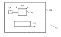
대안적으로, 타겟(120)과 기판(110) 사이의 상대적인 위치가 타겟(120)의 옮김 또는 적합한 회전을 초래함으로써 변화되는 코팅 시스템들에 대하여, 타겟(120)에 영향을 주는 구동 시스템이 제공될 수 있다. 도 2는 코팅 시스템(100)에 대한 이러한 대안을 개략적으로 도시한다. 코팅 시스템(200)에서, 타겟은 타겟 흔들림 방향(206)을 따른 층 형성 동안 이동가능하도록 구성된다. 이러한 실시예들에서, 기판(110)은 전체 층 형성 프로세스 동안 진공 챔버(102)에 대하여 정지를 유지할 수 있다. 게다가, 코팅 시스템(200)은 본 명세서에서의 실시예들에 따라 타겟(120)을 이동하도록(특히 흔들도록) 적응된 타겟 흔들림 구동 시스템(208)을 포함한다. 예시적인 시스템에서, 타겟 흔들림 구동 시스템(208)은 기판 흔들림 방향(106)을 따른 타겟(120)의 옮김을 초래한다. 대안적으로, 타겟 흔들림 구동 시스템(208)은, 평면 타겟에 대하여 아래에 더 논의된 바와 같이, 타겟(120)의 세로축에 대한 타겟(120)의 회전을 초래할 수 있지만, 이에 제한되지 않는다. 타겟 흔들림 구동 시스템(208)(기판 흔들림 구동 시스템(108)과 유사한)은 타겟(120)의 이동을 초래함으로써 타겟-기판 상대적인 위치를 적절하게 변경하기 위한 적합한 구동 시스템(미도시)을 포함할 수 있다. Alternatively, for a coating system where the relative position between the
어떤 실시예들에 따르면, 기판(110)에 걸쳐 타겟으로부터 물질을 스퍼터링하는 것은 (a) 타겟(120)과 기판(110) 사이의 상대적인 위치를 제 1 위치(Ⅰ)로 변경하는 것 - 상대적인 위치는 제 1 위치(Ⅰ)에 유지됨 -; 및 타겟(120)과 기판(110) 사이의 상대적인 위치를 제 2 위치(Ⅱ)로 변경하는 것을 포함한다. 일반적인 실시예들에 따르면, 상대적인 위치들은 선택된 시간 간격 동안 유지되고, 즉, 제 1 위치는 미리 결정된 제 1 시간 간격 동안 유지되며, 제 2 위치(Ⅱ)는 미리 결정된 제 2 시간 간격 동안 유지된다. 제 1 위치(Ⅰ) 및 제 2 위치(Ⅱ)는 기판(110) 및/또는 타겟(120) 사이의 상대적인 위치의 변경을 초래하는 흔들림 변위의 외곽 위치들에 각각 대응될 수 있다. According to some embodiments, sputtering material from a target across the
본 명세서에서의 임의의 실시예와 결합될 수 있는 어떤 실시예들에 따르면, 미리 결정된 제 1 시간 간격은 적어도 0.1초, 바람직하게는 적어도 0.5초, 더욱 바람직하게는 적어도 1초이다. 시간 간격들에 대하여, 적어도 10초와 같은, 또는, 훨씬 많은 적어도 30초와 같은 더 큰 미리 결정된 시간들이 또한 가능하다. 특히, 상대적인 위치는 외곽 위치들(즉, 제 1 및 제 2 위치)에서 전체 층 형성 프로세스의 미리 결정된 퍼센트 또는 이의 적어도 40% 또는, 더 명확하게, 이의 적어도 20% 또는, 더욱 명확하게는, 이의 적어도 10%와 같은 스퍼터링 시간 또는 40 내지 10% 또는 40 내지 20% 또는 20 내지 10%와 같은 이들 퍼센트들 사이의 시간 간격 동안 유지될 수 있다. According to certain embodiments that may be combined with any embodiment herein, the predetermined first time interval is at least 0.1 seconds, preferably at least 0.5 seconds, more preferably at least 1 second. For time intervals, larger predetermined times, such as at least 10 seconds, or even more, at least 30 seconds, are also possible. In particular, the relative position may be a predetermined percentage or at least 40% or more specifically, at least 20% or more clearly thereof of the entire layer formation process at the outer positions (ie, the first and second positions). Sputtering time such as at least 10% or a time interval between these percentages such as 40-10% or 40-20% or 20-10%.
층 형성 프로세스는 물질이 스퍼터링되고 있는 프로세싱 시간 및 물질이 스퍼터링되지 않는 프로세싱 시간(예를 들면, 경우에 따라서 물질이 타겟으로부터 스퍼터링되지 않는 동안 타겟-기판 상대 위치의 최종 변경 동안과 같은 하나의 층의 형성 동안 2개의 스퍼터링 간격들 사이)을 포함함에 주의해야 한다. 스퍼터링은 타겟(120)과 기판(110) 사이의 상대적인 위치가 층 형성 프로세스 동안 정지를 유지하는 제 1 및 제 2 위치와 같은 이들 위치들에서만 수행될 수 있다. 그런 경우에, 전체 스퍼터링 시간에 대하여 상대적인 위치가 외각 위치들에서 유지될 수 있는 시간의 미리 결정된 퍼센트는 대략 100%이다. 이에 의해, 특히 고 균일성이 달성될 수 있다. The layer formation process may be performed by one layer such as the processing time at which the material is being sputtered and the processing time at which the material is not sputtered (e.g. during the last change of target-substrate relative position while the material is not sputtered from the target in some cases). It is to be noted that it includes (between two sputtering intervals) during formation. Sputtering may be performed only at these locations, such as the first and second locations, where the relative location between the
본 발명의 실시예들에 따르면, 층 형성 프로세스 동안, 기판(110) 및/또는 타겟(120)은 미리 결정된 제 1 시간 동안 제 1 상대적인 위치로 변위된다. 이러한 제 1 상대적인 위치는 도 1 및 도 2에서의 위치(Ⅰ)에 대응한다. 그 다음, 기판(110) 및 타겟(120)은 미리 결정된 제 2 시간 동안 제 2 상대적인 위치(도 1 및 도 2에서의 위치(Ⅱ))로 변위된다. 상대적인 위치의 이러한 변위는 스퍼터링된 물질이 기판(110)에 걸쳐 비대칭적으로 분포되고 있음을 초래할 수 있다. 이러한 비대칭 분포는 코팅 룸 내의 기판 홀더 또는 벽들과 같은 코팅을 필요로 하지 않는 영역들의 더 높은 코팅율을 초래할 수 있고, 그에 의해 프로세스 효율을 감소시킬 수 있다. 그러나, 이러한 상황에도 불구하고, 놀랍게도, 그에 의해 기판 상에 증착된 층의 동질성은 기판과 타겟 사이의 상대적인 위치가 프로세스 동안 변화되지 않고 유지되는 층 형성 프로세스에 비하여 증가될 수 있음이 본 발명의 발명자들에 의해 발견되었다. 이러한 문맥 내에서, 층의 동질성은 일반적으로 기판 상의 코팅된 영역 전반에 걸친 층 두께, 결정 구조, 특정 저항 및/또는 층 응력의 균일성으로 지칭됨에 주의해야 한다. According to embodiments of the present invention, during the layer formation process, the
실시예들에 따르면, 타겟(120)은 회전가능한 타겟 또는, 더 특별히, 그의 원통형 대칭축에 대하여 회전가능한 실질적으로 원통형 타겟이다. 대안적인 실시예들에 따르면, 타겟(120)은 평면 타겟(즉, 스퍼터링되도록 적응된 타겟 표면을 갖고 이 표면이 실질적으로 평면인 타겟)이다. 일반적으로, 이러한 평면 타겟은, 도 5에 대하여 아래에 더 설명된 바와 같이, 평면 캐소드 조립체와 결합된다(즉, 그의 일부를 형성한다). 이러한 대안적인 실시예들에서, 타겟(120)과 기판(110) 사이의 상대적인 위치는 왕복 방식으로 평면 타겟(120)을 회전시킴으로써 변경될 수 있다. 특히, 평면 타겟(120)은 그의 세로축에 대하여, 즉, 스퍼터링될 타겟 표면에 실질적으로 평행하고 타겟 바디를 가로지르는 축에 대하여 회전될 수 있다. 평면 타겟을 참조하는 실시예들의 더 세부사항들은 아래에 더 논의된다(도 5 및 도 7을 참조하는 구절들을 참조). According to embodiments,
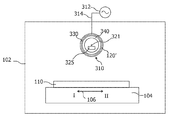
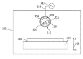
도 3은 본 명세서에서 더 상세하게 설명된 실시예들에서 사용된 바와 같은 캐소드 조립체(310)를 예시적으로 도시한다. 도 3에 도시된 모든 엘리먼트들은 또한 본 명세서에서 설명된 실시예들, 특히, 도 1 및 도 2에 대하여 설명된 이들 실시예들의 적어도 일부와 결합될 수 있음이 이해될 것이다. 도 3은 배킹 튜브(baking tube)(330) 상에 배치되는 회전가능한 원통형 타겟(120')을 도시한다. 특히, 회전가능한 원통형 타겟(120')은 배킹 튜브(330)와 접할 수 있지만, 이에 제한되지 않는다. 일반적으로 타겟(120')의 물질은 타겟(120')이 원통형 대칭의 그것의 축에 대하여 회전하고 있으면서 스퍼터링 동안 세정된다. 어떤 실시예들에 따르면, 캐소드 조립체(310)는 스퍼터링 프로세스로부터 초래될 수 있는 타겟 상의 고온들을 감소시키기 위해 냉각 시스템(340)을 포함한다. 예를 들면, 냉각 시스템(340)은 물 또는 임의의 다른 적합한 냉각 물질과 같은 냉각 물질을 포함하는 튜브로 구성될 수 있지만, 이에 제한되지 않는다. 스퍼터링 프로세스에 투입되는 에너지의 주요 부분 - 일반적으로 수 킬로 와트의 자릿수로 -이 타겟으로 전달된 열로 전환될 수 있기 때문에, 냉각이 유리할 수 있다. 어떤 상황들에서, 이러한 열은 타겟을 손상시킬 수 있다. 다른 실시예들에 따르면, 캐소드 조립체(310)의 내부 전체는 적합한 냉각 물질로 충진된다. 3 illustratively shows a
도 3의 개략도에 도시된 바와 같이, 캐소드 조립체(310)는 자석 조립체(325)를 포함할 수 있다. 예시적인 실시예에서, 자석 조립체(325)는 배킹 튜브(330) 내에 위치된다. 본 명세서에서의 실시예들에 따르면, 캐소드 조립체는 배킹 튜브(330) 내에 2개, 3개 또는 훨씬 많은 임의의 적절한 수의 자석 조립체들을 포함할 수 있다. 캐소드 조립체(310)는 적어도 배킹 튜브(330), 그 결과 타겟(120)의 회전을 수행하기 위한 구동 시스템(미도시)에 결합된 샤프트(312)를 포함할 수 있다. 예시적인 실시예에서, 샤프트(312)의 위치는 타겟(120')의 원통형 대칭축에 대응한다. 그에 의해 회전식 타겟은 본 명세서에서의 실시예들에 따른 코팅 시스템에서 실시될 수 있으며, 이는 타겟 물질의 더 높은 활용을 용이하게 할 수 있다. 예시적인 실시예에서, 타겟(120)을 스퍼터링하는 이러한 회전은 그 위의 스퍼터링된 물질의 매우 균일한 층의 형성을 용이하게 하기 위한 기판의 수평 옮김과 통합된다(combined). 대안적으로, 타겟(120)을 스퍼터링하는 이러한 회전은 전체 캐소드 조립체(310)의 흔들림과 같은, 그러나 이에 제한되지 않는 본 명세서에서의 실시예들에 따라 타겟(120)과 기판 사이의 상대적인 위치를 변경하기 위한 적합한 임의의 다른 방법과 통합될 수 있다. As shown in the schematic diagram of FIG. 3, the
본 발명의 양상에 따르면, 타겟에 결합된 캐소드 조립체에 인가된 전압은 기판에 걸쳐 스퍼터링된 물질의 층의 형성 동안 시간에 대해 변경된다. 다시 말해서, 일정하지 않은 전압이 스퍼터링 동안 캐소드 조립체에 인가될 수 있다. 특히, 스퍼터 전력은 보통 캐소드 조립체에 인가된 전압에 바로 대응한다. 0V에 근접한 값 이외에, 인가된 전압과 스퍼터 전력 사이의 관계는 대략 선형이다. 따라서, 어떤 실시예들에 따르면, 스퍼터 전력은 기판(110)과 타겟(120) 사이의 상대적인 위치에 따라 변화될 수 있다. According to an aspect of the present invention, the voltage applied to the cathode assembly coupled to the target is changed over time during the formation of a layer of sputtered material across the substrate. In other words, a non-uniform voltage may be applied to the cathode assembly during sputtering. In particular, sputter power usually corresponds directly to the voltage applied to the cathode assembly. In addition to values close to 0V, the relationship between the applied voltage and the sputter power is approximately linear. Thus, in some embodiments, the sputter power may vary depending on the relative position between the
도 3에 도시된 예시적인 실시예에서, 전압은 전압 공급장치(312)에 의해 캐소드 조립체(310)(타겟(120")에 결합된)에 인가된다. 특히, 전압 공급장치(312)는 배킹 튜브(330)에 음전위를 인가하기 위해 전기 연결(314)을 통하여 배킹 튜브(330)에 전기적으로 연결될 수 있다. 배킹 튜브(330)는 배킹 튜브(330)가 전극으로서 동작될 수 있도록 적합한 물질로 구성된다. 이러한 적합한 물질은 구리와 같은, 그러나 그에 제한되지 않는 금속일 수 있다. 어떤 실시예들에 따르면, 양극(즉, 스퍼터링 동안 양전위를 가질 수 있고 또한 애노드로 지칭되는 전극)은 스퍼터 프로세스를 용이하게 하기 위해 타겟(120")에 근접하게 위치된다. In the example embodiment shown in Figure 3, the voltage is applied to the cathode assembly 310 (coupled to the
따라서, 본 명세서에서의 실시예들에 따르면, 전계는 캐소드 조립체(310)에 인가된 전압에 의해 예시적인 타겟들(120 및 120')과 같은, 그러나 이에 제한되지 않는 타겟에 결합될 수 있다. Thus, according to embodiments herein, the electric field may be coupled to a target, such as, but not limited to, example targets 120 and 120 'by the voltage applied to the
본 발명자들은 본 명세서에서의 실시예들에 따라 형성된 층의 균일성은 타겟-기판 상대적인 위치가 위에 언급된 제 1 및 제 2 위치들에서 얼마나 오래 유지되는지에 따라 더 개선될 수 있음을 관찰하였다. 특히, 타겟-기판 상대적인 위치가 제 1 및 제 2 위치들에서 전체 프로세스 시간에 비교하여 더 오래 유지될수록, 더 우수한 동질성 및, 특히, 균일성이 획득된다. 따라서, 최대 동질성은 이들 위치들에서 스퍼터링함으로써 달성될 수 있다. 이동시(즉, 타겟-기판 상대적인 위치가 변경되고 있는 경우)에 스퍼터링 전계를 끄는 것이 더 가능하며, 이는 균일성을 더 증가시킬 수 있다. The inventors have observed that the uniformity of the layer formed according to the embodiments herein can be further improved depending on how long the target-substrate relative position is maintained at the above mentioned first and second positions. In particular, the longer the target-substrate relative position is maintained compared to the overall process time at the first and second positions, the better homogeneity and, in particular, uniformity is obtained. Thus, maximum homogeneity can be achieved by sputtering at these locations. It is more possible to turn off the sputtering field at the time of movement (ie when the target-substrate relative position is being changed), which can further increase uniformity.
특히, 본 발명의 발명자들은 층 동질성이 상대적인 위치가 변경될 때 전계가 감소되거나 꺼지면, 더 증가될 수 있음을 발견하였다. 더 특별히, 동질성은 기판과 타겟 사이의 상대적인 위치가 흔들림 외곽 위치들에 대응하지 않을 때 스퍼터링이 중지되면, 증가될 수 있다. 스퍼터링은 타겟에 결합된 캐소드 조립체와 결합된 애노드 사이의 전위차를 0에 근접하거나 0으로 설정함으로써 중지될 수 있다. In particular, the inventors of the present invention have found that the layer homogeneity can be increased further if the electric field is reduced or turned off when the relative position is changed. More particularly, homogeneity may be increased if sputtering stops when the relative position between the substrate and the target does not correspond to the outer position of shake. Sputtering can be stopped by setting the potential difference between the cathode assembly coupled to the target and the anode coupled to zero or setting it to zero.
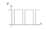
따라서, 어떤 실시예들에 따르면, 상기 상대적인 위치를 변경하는 것은 위에 언급된 상대적인 위치의 제 1 위치로부터 제 2 위치로의 변경을 포함하고, 여기서, 타겟(120)에 결합된 캐소드 조립체(310)에 공급되는 전압은 상대적인 위치가 상기 제 1 위치와 상기 제 2 위치 사이의 위치에 대응할 때보다 상대적인 위치가 제 1 위치 또는 제 2 위치에 대응할 때 더 높다. 특히, 전압은 상기 상대적인 위치가 제 1 및 제 2 위치 사이의 위치에 대응할 때 실질적으로 0일 수 있다. 더 특별히, 전압은 상기 상대적인 위치의 변경 동안 구형파에 따라 시간에 대해 변경될 수 있다. Thus, according to some embodiments, changing the relative position comprises changing from the first position to the second position of the relative position mentioned above, wherein the
도 4는 이들 실시예들에 대해 애노드와 캐소드 조립체 사이에 인가된 전압(V)을 도시하면, 여기서, 전압은 때에 맞추어 일정하지 않지만 구형파의 형상을 갖는다. 도면에서 알 수 있는 바와 같이, 전압은 일반적으로 제 1 또는 제 2 시간 스퍼터링 간격(즉, 상대적인 위치가 변화되지 않고 유지되는 경우)인 얼마 동안 어떤 일정한 0이 아닌 레벨을 유지한다. 전압은 그 다음 어떤 시간 간격들에서 실질적으로 감소된다. 이들 시간 간격들은 일반적으로 상대적인 위치가 변경되고 있을 때, 예를 들면, 상대적인 위치가 위에서 언급된 제 1 위치로부터 제 2 위치로 변경하는 때의 시간들에 대응한다. FIG. 4 shows the voltage V applied between the anode and cathode assembly for these embodiments, where the voltage is not constant in time but has the shape of a square wave. As can be seen in the figure, the voltage maintains some constant non-zero level for some time, which is generally the first or second time sputtering interval (ie, when the relative position remains unchanged). The voltage is then substantially reduced at certain time intervals. These time intervals generally correspond to the times when the relative position is changing, for example when the relative position changes from the above mentioned first position to the second position.
어떤 실시예들에 따르면, 전압은 그것이 실질적으로 감소될 때에 0V일 수 있다. 그에 의해, 스퍼터링은 거의 즉각 정지한다. 대안적인 실시예들에 따르면, 전압은 스퍼터링 프로세스 동안 초기 전압으로 적합할 수 있는 어떤 임계값으로 감소될 수 있다. 예를 들면, 이러한 임계 전압은 스퍼터링을 정지할 수 있지만, 스퍼터 프로세스의 더 빠른 재시작을 허용할 수 있다. 그러나, 기판(110)과 타겟(120) 사이의 상대적인 위치가 변화되고 있을 때, 전압은 스퍼터 전압의 10%보다 작은(더 일반적으로 5%보다 적은)스퍼터 전압의 값으로 감소될 수 있다. According to some embodiments, the voltage may be 0V when it is substantially reduced. Thereby, sputtering stops almost immediately. According to alternative embodiments, the voltage may be reduced to some threshold that may be suitable as the initial voltage during the sputtering process. For example, such a threshold voltage may stop sputtering, but may allow for a faster restart of the sputter process. However, when the relative position between the
위에서 설명된 바와 같이, 일정하지 않은 전압이 스퍼터링 동안 캐소드 조립체(310)에 인가될 수 있다. 일반적인 실시예들에 따르면, 전압은 타겟(120)과 기판(110) 사이의 상대적인 위치와 동조된다(synchronized). 예를 들면, 전압은 자석 조립체의 이동 동안 캐소드 조립체(310)에 인가되는 최대 전압 값의 35%보다 작은 값 또는, 더 특별히, 20%보다 작은 값으로 설정될 수 있다. 도 10은 사인파 형상을 따르는 시간 t에 대하여 변하는 전압 V를 예시적으로 도시한다. 상대적인 위치는 사인파 전압 V에 동조될 수 있다. 예를 들면, 상대적인 위치는 전압 V가 도 10에 도시된 점선보다 큰(즉, 위의) 시간들에서 변화되지 않고 유지될 수 있지만, 이에 제한되지 않는다. 전압 V가 점선 보다 작은(즉, 아래의) 시간들 동안, 상대적인 위치는 제 1 위치로부터 제 2 위치로 그리고 교차 방식으로 반대로 변경될 수 있다. As described above, a non-uniform voltage may be applied to the
본 명세서에서의 다른 실시예들과 통합될 수 있는 어떤 실시예들에 따르면, 상대적인 위치는 전체 형성 프로세스 동안 단지 한번 제 1 위치로부터 제 2 위치로 변경된다. 대안적인 실시예들에 따르면, 상대적인 위치는 제 1 위치로부터 제 2 위치로 그리고 그 반대로 변경된다. 이러한 이동들의 순서는 전체 형성 프로세스 동안 다수 회 반복될 수 있다. 예를 들면, 상대적인 위치는 기판을 코팅하는 경우, 상대적인 위치가 각각 제 1 및 제 2 위치에 2번 이상 대응하도록 3회 이상 변화될 수 있다. 이러한 이동 패턴은 이동들의 순서를 이루고, 결국 중간의 스퍼터링 전력을 변경하기 위해 필요한 시간 때문에 전체 프로세스 시간을 증가시킬 수 있으며, 그것은 층 동질성의 추가 증가를 초래할 수 있다. According to some embodiments, which may be integrated with other embodiments herein, the relative position is changed from the first position to the second position only once during the entire forming process. According to alternative embodiments, the relative position is changed from the first position to the second position and vice versa. The order of these movements can be repeated many times during the entire formation process. For example, the relative position may be changed three or more times so that when the substrate is coated, the relative position corresponds two or more times to the first and second positions, respectively. This movement pattern is in order of movements, which in turn can increase the overall process time because of the time needed to change the intermediate sputtering power, which can lead to further increases in layer homogeneity.
어떤 실시예들에 따르면, 스퍼터링된 물질의 층을 형성하는 단계는 (ⅰ) 스퍼터링을 위한 전계가 켜져 있으면서 제 1 시간 간격 동안 제 1 위치에서 기판(110)과 타겟(120) 사이의 상대적인 위치를 유지하는 단계; (ⅱ) 제 1 시간 간격이 경과한 후, 기판(110)과 타겟(120) 사이의 상대적인 위치를 제 2 위치로 설정하는 단계(예를 들면, 도 1에 도시된 바와 같이, 기판(110)의 변위에 의해, 또는 도 2에 도시된 바와 같이, 타겟(120)의 변위에 의해), 전계는 제 1 위치로부터 제 2 위치로의 상대적인 위치의 변경 동안 꺼짐; (ⅲ) 전계가 켜져 있으면서 제 2 시간 간격 동안 제 2 위치에서 기판(110)과 타겟(120) 사이의 상대적인 위치를 유지하는 단계를 포함한다. 따라서, 단계들 (ⅱ) 및 (ⅰ)은 그 다음 상대적인 위치를 제 2 위치로부터 제 1 위치로 변경하기 위한 이러한 순서로 유사하게 수행될 수 있다. 구절 "전계가 켜짐"은 전압이 타겟(120)에 결합된 캐소드 조립체 및 그에 결합된 애노드에 인가되고 있는 것으로 이해된다. 일반적인 실시예들에 따르면, 인가된 전압은 제 1 시간 간격 및/또는 제 2 시간 간격 동안 일정하다. 인가된 전압은 상대적인 위치가 제 1 위치에 대응하는 시간들 및 상대적인 위치가 제 2 위치에 대응하는 시간들에서 동일할 수 있다. According to some embodiments, the step of forming a layer of sputtered material comprises (i) determining the relative position between the
도 5 및 도 7에 도시된 어떤 실시예들에 따르면, 기판을 코팅하기 위한 시스템이 제공되고, 여기서, 코팅 시스템들은 기판 상에 물질을 스퍼터링하기 위한 하나 또는 둘 이상의 평면 타겟들을 포함한다. 이들 실시예들에서 적어도 하나의 평면 타겟은 상기 기판의 코팅 동안 왕복 방식으로 회전가능하다. 본 명세서에서 사용된 바와 같은 용어 "왕복 방식으로 회전가능한"은 앞-뒤 운동을 따라 회전가능한 것, 즉, 평면 타겟을 제 1 위치로 회전시키고, 평면 타겟을 제 1 위치로부터 제 2 위치로 다시 회전시키는 것으로 이해되어야 한다. 제 1 위치 및 제 2 위치는 또한 평면 타겟의 회전의 외곽 위치들로 지칭된다. 어떤 실시예들에 따르면, 평면 타겟은 스퍼터링을 용이하게 하기 위해 평면 캐소드 조립체에 결합된다. 평면 타겟의 회전은 전체 캐소드 조립체의 회전에 의해 이루어질 수 있다. 특정 실시예들에 따르면, 평면 타겟은 기판 표면에 평행한 축에 대하여, 특히 평면 타겟의(또는 그와 결합된 평면 캐소드의) 세로축에 대하여, 더 특별히, 평면 타겟의(또는 그와 결합된 평면 캐소드의) 중앙축에 대하여 회전가능하다. According to certain embodiments shown in FIGS. 5 and 7, a system for coating a substrate is provided, wherein the coating systems include one or more planar targets for sputtering material on the substrate. In these embodiments at least one planar target is rotatable in a reciprocating manner during the coating of the substrate. The term "rotatable in a reciprocating manner" as used herein refers to something rotatable along a forward-backward motion, that is, rotating a planar target to a first position and backing the planar target from a first position to a second position. It should be understood to rotate. The first position and the second position are also referred to as the outer positions of the rotation of the planar target. According to some embodiments, the planar target is coupled to the planar cathode assembly to facilitate sputtering. Rotation of the planar target can be achieved by rotation of the entire cathode assembly. According to certain embodiments, the planar target is in relation to an axis parallel to the substrate surface, in particular with respect to the longitudinal axis of the planar target (or to the planar cathode associated therewith), more particularly to the plane of the planar target (or associated with it). Rotatable about a center axis of the cathode.
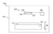
도 5는 평면 타겟(120")에 결합된 평면 캐소드 조립체(502)를 포함하는 다른 예시적인 코팅 시스템(500)을 도시한다. 도 3에 도시된 모든 엘리먼트들은 또한 본 명세서에서 설명된 실시예들의 적어도 일부와, 특히, 도 1 및 도 2에 대하여 설명된 실시예에 통합될 수 있음이 이해될 것이다. 평면 캐소드 조립체(502)는 평면 타겟(120")에 지지체를 제공하는 평면 배킹 바디(530)를 포함한다. 특히, 평면 타겟(120")은 평면 배킹 바디(530)에 접할 수 있다. 평면 배킹 바디(530)는 전압 소스(본 도면에서 미도시)에 연결될 수 있고, 그래서 배킹 바디(530)는 전극으로서 기능한다(배킹 튜브(330)에 대하여 위에서 설명된 바와 유사한 방식으로). 캐소드 조립체(502)는 본 명세서에서 설명된 바와 같은 타겟(120")으로부터 스퍼터링을 생성하기 위해 적합한 전계를 제공하기 위한 애노드(미도시)와 결합될 수 있다. 평면 캐소드 조립체(502)는 본 명세서에서 설명된 바와 같은 마그네트론 스퍼터링하기 위한 자석 조립체 및/또는 냉각 시스템과 같은, 그러나 이에 제한되지 않는 도 5에 도시되지 않은 다른 엘리먼트들을 포함할 수 있다. 5 illustrates another
평면 타겟(120")은 기판(110)을 코딩하는 동안 평면 타겟(120")과 기판(110) 사이의 상대적인 위치가 변경되도록 왕복 방식으로 회전가능하다. 특히, 평면 타겟(120")은 피벗축(504)에 대하여 변경될 수 있다. 예시적인 실시예에서, 피벗축(504)은 평면 캐소드 조립체(502)의 중앙축에 대응한다. 본 명세서에서의 실시예들에 따르면, 피벗축(504)은 코팅될 기판(110)의 표면에 평행한 축, 예를 들면, 타겟(120")의 세로축에 대응할 수 있지만, 그러나 이에 제한되지 않는다. 특히, 피벗축(504)은 캐소드 조립체(502) 또는 타겟 조립체(120")의 중심선의 축에서 벗어날 수 있다. 일반적으로, 피벗축(504)은 대응하는 회전이 타겟(120")과 기판(110) 사이의 상대적인 위치의 변경을 초래하는 한 임의의 축에 대응할 수 있다. The
도 5는 평면 타겟(120")이 상대적인 위치를 변경하기 위해 회전될 수 있는 각들 β 및 -β를 도시한다. 각 β는 평면 타겟(120")에 수직인 축 및 기판(110)에 수직인 축(512)에 의해 형성된 각이다. 선들(508 및 510)은 그의 외곽 위치들에서 평면 타겟(120")에 수직인 축들을 도시한다. 각의 값은 타겟(120")의 시계 방향 회전에 대하여 양이고, 반시계 방향 회전에 대하여 음이다. 각들의 값들은 평면 타겟(120")이 코팅될 기판(110)의 표면에 대하여 평행하게 위치되는(positioned) 경우 0에 대응한다. 따라서, 타겟(120")의 외곽 위치들(즉, 위에서 언급된 제 1 및 제 2 위치)에서, 평면 각 β는 0이 아닌 값에 대응한다. 예시적인 실시예에서, 각의 절댓값은 타겟의 외곽 위치들 모두(즉, 위에서 언급된 제 1 및 제 2 위치들)에 대하여 동일하다. 대안적으로, 각의 절댓값은 하나의 외곽 위치로부터 다른 외곽 위치로 상이할 수 있다. 일반적인 실시예들에 따르면, 각의 절댓값은 50도보다 작거나, 더 명확하게는, 45도보다 작거나, 더욱 명확하게는, 30도보다 훨씬 작다. Figure 5 shows angles β and -β with which the
일반적인 실시예들에 따르면, 타겟(120")의 회전은 피벗축(504)에 배치된 샤프트(미도시)에 의해 이루어질 수 있다. 이러한 샤프트는 타겟(120")의 왕복 회전을 발생시키는 타겟 흔들림 구동 시스템(208)에 결합될 수 있다. 예를 들면, 타겟 흔들림 구동 시스템(208")은 피벗축(504)에 대한 모터에 의해 발생된 회전력을 커플링하기 위한 전기-기계식 모터(미도시) 및 샤프트(미도시)를 포함할 수 있고, 그래서, 타겟(120")의 왕복 회전이 발생되지만, 이에 제한되지 않는다. According to general embodiments, the rotation of the
코팅 시스템(500)(그러나, 이에 제한되지 않음)과 관련된 어떤 실시예들에 따르면, 기판(110)을 코팅하기 위한 방법이 제공되는데, 이 방법은 상기 기판(110) 상에 스퍼터링된 물질의 층을 형성하는 단계를 포함하고, 여기서, 스퍼터링된 물질의 층을 형성하는 단계는 기판(110)에 걸쳐 평면 타겟(120")으로부터 물질을 스퍼터링하는 단계; 및 평면 타겟(120")을 왕복 방식으로 회전함으로써 타겟(120")과 기판(110) 사이의 상대적인 위치를 변경하는 단계를 포함한다. According to certain embodiments associated with, but not limited to,
이들 후자의 실시예들은 임의의 적합한 회전 패턴을 따라 타겟(120")과 기판(110) 사이의 상대적인 위치를 변경할 수 있다. 예를 들면, 평면 타겟은 일정한 각속도로 회전될 수 있다. 대안적으로, 회전은 일정하지 않은 각속도로 이루어질 수 있다. 게다가, 왕복 회전은 외곽 위치에서 실질적으로 부동 시간 없이 이루어질 수 있다. 대안적인 실시예들에 따르면, 평면 타겟(120")을 회전시키는 단계는, 위에서 설명된 바와 유사한 방식으로, 타겟(120")을 제 1 위치로 회전시키는 단계, 여기서, 제 1 위치는 미리 결정된 제 1 시간 간격 동안 유지됨, 및 상기 적어도 하나의 타겟을 제 2 위치로 회전시키는 단계, 여기서, 제 2 위치는 미리 결정된 제 2 시간 간격 동안 유지됨을 포함한다. 일반적으로, 제 1 및 제 2 위치는 평면 타겟(120")의 왕복 회전에서 외곽 위치들에 대응할 수 있다. These latter embodiments may change the relative position between the
코팅 시스템(500)(그러나 이에 제한되지 않음)과 관련된 어떤 실시예들에 따르면, 코팅 단계는 평면 타겟(120")에 전압을 공급하는 단계를 더 포함할 수 있는데, 이 전압은 코팅 동안 시간에 대하여 변경된다. 더 특별히, 코팅 시스템(500)에서 상대적인 위치를 변경하는 단계는 위에서 설명된 바와 같은 전압 변경과 통합될 수 있다. According to certain embodiments related to (but not limited to)
본 명세서에서의 임의의 실시예와 통합될 수 있는 일반적인 실시예들에 따르면, 타겟(120, 120', 또는 120")은 공간적으로 분리되고, 기판(110)의 전면에 배치된 복수의 타겟 엘리먼트들(즉, 타겟 어레이)로 구성될 수 있으며, 그래서 타겟 엘리먼트들로부터 스퍼터링된 물질은 그 위에 증착될 수 있다. 특히, 타겟 엘리먼트들의 각각은 캐소드 조립체의 일부에 결합되거나 일부를 형성할 수 있다. 더 명확하게, 복수의 캐소드 조립체들은 캐소드 조립체들의 어레이로 배열될 수 있다. 특히, 정적 대면적 기판 증착에 대하여, 규칙적으로 배열되는 캐소드 조립체들의 일차원 어레이를 제공하는 것이 일반적이다. 일반적으로, 프로세싱 챔버 내에서 캐소드 조립체들(및 결합된 타겟들)의 수는 2 내지 20이고, 더 일반적으로는 9 내지 16이다. According to general embodiments that can be integrated with any of the embodiments herein, the plurality of
어레이 실시예들에 따르면, 타겟 엘리먼트들과 기판(110) 사이의 상대적인 위치는 타겟 엘리먼트들을 동시에 옮기거나 적합하게 회전시킴으로써 변경될 수 있다. 대안적으로, 상대적인 위치는 타겟 어레이에 대하여 기판(110)을 변위시킴으로써 변경될 수 있다. 일반적으로, 복수의 타겟들과 기판 사이의 상대적인 위치는 코팅 시스템이 본 명세서에서의 실시예들에 따라 기능하도록 하는 임의의 적합한 방식으로 변경될 수 있다. 일반적으로, 타겟 엘리먼트들의 동위상 변위는 증착된 층의 동질성을 더 증가시킨다. According to array embodiments, the relative position between the target elements and the
일반적으로, 그리고 임의의 실시예에 제한되지 않게, 캐소드 조립체들은 서로 등거리로 공간을 두고 떨어질 수 있다. 특히, 타겟은 타겟 엘리먼트들의 어레이를 포함할 수 있다. 게다가, 타겟의 길이는 코팅될 기판의 길이보다 조금 더 클 수 있다. 추가적으로 또는 대안적으로, 캐소드 어레이는 기판의 폭보다 조금 더 넓은 거리에 걸쳐 확장된다. "조금"은 일반적으로 100% 내지 110%의 범위를 포함한다. 조금 더 긴 코팅 길이/폭의 제공은 코팅 동안 경계 효과의 방지를 용이하게 한다. 캐소드 조립체들은 기판(110)으로부터 등거리로 위치될 수 있다. In general, and without being limited to any embodiment, the cathode assemblies may be spaced equidistant from each other. In particular, the target may comprise an array of target elements. In addition, the length of the target may be slightly larger than the length of the substrate to be coated. Additionally or alternatively, the cathode array extends over a distance slightly larger than the width of the substrate. “Slightly” generally encompasses the
어떤 실시예들에 따르면, 복수의 캐소드 조립체들은 기판(110)에 대하여 등거리가 아니고, 호 형상을 따라 배열된다. 호 형상은, 도 6에 개략적으로 도시된 바와 같이, 안쪽 캐소드 조립체들이 외곽 캐소드 조립체들보다 기판(110)에 더 근접하게 위치되는 바와 같은 것일 수 있다. 대안적으로, 호 형상은 외곽 캐소드 조립체들이 안쪽 캐소드 조립체들보다 기판(110)에 더 근접하게 위치되는 바와 같은 것일 수 있다. 산란 거동은 일반적으로 스퍼터링될 물질에 의존한다. 따라서, 애플리케이션에 따라, 즉, 스퍼터링될 물질에 따라, 호 형상 상에 캐소드 조립체들을 제공하는 것은 형성된 층의 동질성을 더 증가시킬 것이다. 호의 방향은 일반적으로 특정 애플리케이션에 의존한다. According to some embodiments, the plurality of cathode assemblies are not equidistant with respect to the
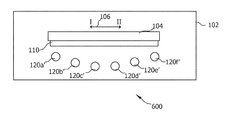
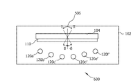
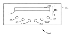
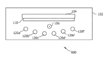
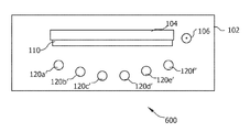
도 6은 기판(110)과 타겟 엘리먼트들(120a' 내지 120f')을 포함하는 타겟 어레이 사이의 상대적인 위치의 변경이 기판 흔들림 방향(106)을 따른 기판(110)의 수평 옮김(특히 그의 흔들림)에 의해 이루어지는 예시적인 코팅 시스템(600)을 도시한다. 예시적인 실시예에서, 타겟 엘리먼트들(120a' 내지 120f')은 회전가능한 원통형 타겟들이다. 대안적인 실시예들에서, 타겟 엘리먼트들은 임의의 적합한 형상을 가질 수 있다. FIG. 6 shows that a change in relative position between the
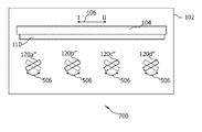
도 7은 평면 타겟들(120a" 내지 120d")의 어레이(120")을 포함하는 다른 예시적인 코팅 시스템(700)을 도시한다. 평면 타겟들(120a" 내지 120d")의 각각은 도 5에 도시된 평면 타겟(120")과 유사하게 구성될 수 있다. 따라서, 예시적인 코팅 시스템(700)에서, 평면 타겟들(120a" 내지 120d")의 어레이 사이의 상대적인 위치의 변경은 피벗 방향(506)에서 각각의 피벗축(504)에 대한 타겟들의 동기 왕복 회전에 의해 이루어진다. 평면 타겟들(120a" 내지 120d")의 각각은 도 5에 대하여 위에서 설명된 바와 유사하게 각 β로 회전될 수 있다. 도면에서, 평면 타겟들(120a" 내지 120d")의 각각 중 하나의 외곽 위치는 굵은 선들에서의 엘리먼트들에 의해 도시되고, 그것의 다른 외곽 위치는 가는 선들에서의 엘리먼트들에 의해 도시된다. 도 7에 도시된 바와 같이, 기판 흔들림 및 타겟 흔들림은 타겟-기판 상대적인 변위를 형성하기 위해 통합될 수 있다. 7 illustrates another
본 발명의 다른 실시예들(특히, 도 6 및 도 7에 도시된 것과 같은 그러나 이에 제한되지 않는 복수의 캐소드들 조립체들을 제공하는 것)과 통합될 수 있는 특정 실시예들에 따르면, 적어도 하나의 타겟으로부터 물질을 스퍼터링하는 단계는 적어도 2개의 실질적으로 상호보완적인 막 분포들을 중첩하는 단계를 포함할 수 있다. 특히, 본 명세서에서 설명된 실시예들은 2개의 실질적으로 상호보완적인 막 분포들이 스퍼터링된 물질의 층의 형성에 의해 중첩하는 방식으로 제 1 위치 및 제 2 위치를 선택하는 단계를 포함한다. "상호보완적인 막 분포"는 상대적인 타겟-기판 위치에서 스퍼터링된 물질의 최대 두께 영역들(제 1 최댓값들)이 그것들이 다른 상대적인 타겟-기판 위치에서 스퍼터링된 물질의 2개의 최대 두께 영역들(제 2 최댓값들) 중간에 배치되도록 분포됨을 의미한다. 더 명확하게, 제 1 및 제 2 최댓값들은 최대 두께로 증착된 층의 영역들이 동일하게 간격을 두도록 분포될 수 있다. 그에 의해, 조금 균일한 층의 형성이 용이하게 된다. According to certain embodiments that can be integrated with other embodiments of the present invention (in particular, providing a plurality of cathode assemblies, such as but not limited to those shown in FIGS. 6 and 7), at least one Sputtering the material from the target may include overlapping at least two substantially complementary film distributions. In particular, the embodiments described herein include selecting the first location and the second location in such a way that two substantially complementary film distributions overlap by the formation of a layer of sputtered material. “Complementary film distribution” means that the maximum thickness regions (first maximums) of the sputtered material at relative target-substrate positions are the two largest thickness regions of the sputtered material at different relative target-substrate positions 2 maximum values). More specifically, the first and second maximums can be distributed such that the regions of the layer deposited with the maximum thickness are equally spaced. Thereby, formation of a slightly uniform layer becomes easy.
특히, 본 명세서에서의 실시예들에 따르면, 적어도 하나의 타겟으로부터 물질을 스퍼터링하는 단계는 주기성 길이 λ를 갖는 기판의 길이를 따라 주기적으로 변경하는 두께를 갖는 적어도 2개의 막 분포들을 중첩하는 단계(도 8에 도시됨)를 포함할 수 있다. 어떤 실시예들에 따르면, 타겟-기판 상대적인 위치를 변경하는 단계는 적어도 2개의 막 분포들이 다른 것에 대한 하나의 위상이 다른 방식으로 수행된다. 예를 들면, 적어도 2개의 막 분포들의 주기성의 위상은 π/2 이하로 상이할 수 있다. In particular, according to embodiments herein, sputtering material from at least one target comprises overlapping at least two film distributions having a thickness that periodically changes along the length of the substrate having a periodic length λ ( 8). According to some embodiments, the step of changing the target-substrate relative position is performed in a manner in which one phase for the at least two film distributions is different. For example, the phase of the periodicity of the at least two film distributions can differ by π / 2 or less.
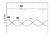
도 8은 2개의 실질적으로 상호보완적인 막 분포들이 중첩되는 실시예를 도시한다. y-축은 막의 높이에 대한 측량 단위를 나타내는 한편, x-축은 기판의 길이에 대한 측량 단위를 나타낸다. 증착은 각 증착 설정이 실질적으로 사인파 막 분포들을 초래하도록 캐소드 조립체들의 어레이에 의해 발생한다. 2개의 증착 프로파일들은 2개의 상이한 위치들에서의 스퍼터링으로부터 초래된 프로파일들이다. 예시에서, 제 1 막 분포(802)는 제 1 타겟-기판 상대적인 위치에서 형성된다. 예시에서, 타겟과 기판 사이의 상대적인 위치는 제 2 타겟-기판 상대적인 위치로 변경된다. 8 illustrates an embodiment in which two substantially complementary film distributions overlap. The y-axis represents the unit of measurement for the height of the film, while the x-axis represents the unit of measurement for the length of the substrate. Deposition occurs by an array of cathode assemblies such that each deposition setup results in substantially sinusoidal film distributions. The two deposition profiles are profiles resulting from sputtering at two different locations. In an example, the
상대적인 위치는 본 명세서에서의 실시예들 중 어느 것에 따라 변경될 수 있다. 예를 들면, 기판은 수평 방향을 따라 옮겨질 수 있거나, 타겟(또는 타겟 어레이)은 위에서 설명된 바와 같이 옮겨지거나 적절하게 회전될 수 있다. 제 2 타겟-기판 위치에서, 제 2 막 분포(804)는 본 명세서에서의 실시예들에 따라 형성된다. 양자의 막 분포들의 중첩으로부터, 제 1 및 제 2 막 분포들보다 더 높은 균일성을 갖는 층(806)이 초래된다. 도 8에 도시된 개략도에서, 막 두께 및 기판 길이(X)는 임의의 단위(a.u.)로 도시됨에 주의해야 한다. The relative position may change in accordance with any of the embodiments herein. For example, the substrate may be moved along the horizontal direction, or the target (or target array) may be moved or appropriately rotated as described above. At the second target-substrate position, the
어떤 실시예들에 따르면, 타겟과 기판 사이의 상대적인 위치는 층 형성 동안 위에서 언급된 제 1 및 제 2 위치 이외의 다른 위치들에서 미리 결정된 시간들 동안 정지되게 위치될 수 있다. 그에 의해 층의 균일성은 더 향상될 수 있다. 이러한 추가 위치들은 제 1 및 제 2 위치들 중간에 배치된다. 예를 들면, 상대적인 위치는 제 3 미리 결정된 시간의 주기(즉, 제 3 시간 간격)에 대한 제 3 위치에 또는 결국, 제 4 미리 결정된 시간의 주기(즉, 제 4 시간 간격)에 대한 제 4 위치에 위치될 수 있다. 상대적인 위치는 층 형성 동안 더 추가 위치들에서 정지를 유지할 수 있다. According to some embodiments, the relative position between the target and the substrate may be stationary for predetermined times at positions other than the first and second positions mentioned above during layer formation. Thereby, the uniformity of the layer can be further improved. These additional positions are arranged in between the first and second positions. For example, the relative position may be at a third position relative to a third predetermined period of time (ie, a third time interval) or eventually to a fourth position relative to a fourth predetermined period of time (ie, a fourth time interval). May be located at a location. The relative position may keep stationary at further positions during layer formation.
본 발명의 발명자들은 이러한 추가 위치들이 증착된 층의 더 높은 동질성의 정도를 용이하게 함을 발견하였다. 특히, 스퍼터링된 물질의 층의 형성은 복수의 서브-층들을 중첩하는 단계를 포함할 수 있고, 각 서브-층은 미리 결정된 스퍼터링 전압으로 미리 결정된 상대적인 타겟-기판 위치에서 증착될 수 있다. 예를 들면, 각 서브-층은 평면 타겟 엘리먼트들의 어레이에 의해 증착될 수 있고(도 8에 도시된 바와 같이), 각 타겟 엘리먼트들은 코팅될 기판의 표면에 수직인 축에 대하여 각 β를 형성할 수 있다. The inventors of the present invention have found that these additional positions facilitate the higher degree of homogeneity of the deposited layer. In particular, the formation of a layer of sputtered material can include overlapping a plurality of sub-layers, each sub-layer can be deposited at a predetermined relative target-substrate location with a predetermined sputtering voltage. For example, each sub-layer may be deposited by an array of planar target elements (as shown in FIG. 8), each target element forming an angle β about an axis perpendicular to the surface of the substrate to be coated. Can be.
이러한 후자의 실시예들에 대하여, 본 발명자들은 아크(arcing)가 프로세스 전력들 및 평면 타겟들의 각들의 증가와 비-선형적으로 증가함을 관찰했다. 본 발명자들은 이러한 실시예들에 대하여, 높은 균일도는 몇몇 서브-층들(예를 들면, 4개의 서브-층들)의 중첩에 의해 획득될 수 있으며, 여기서, 각 서브-층은 특정 전압 및 특정 각으로 증착됨을 발견하였다. 예를 들면, 높은 균일성은 몇몇 서브-층들을 중첩함으로써 획득될 수 있고, 높은 각들로 스퍼터링된 서브-층들은 낮은 스퍼터링 전압에 대응하며, 낮은 각들로 스퍼터링된 서브-층들은 높은 스퍼터링 전압들에 대응한다. 그에 의해, 높은 수율 시간 및 층 균일성이 최적화될 수 있다. For these latter embodiments, the inventors observed that arcing increases non-linearly with the increase in the angles of the process powers and planar targets. The inventors have found that for these embodiments, high uniformity can be obtained by overlapping several sub-layers (eg, four sub-layers), where each sub-layer is at a specific voltage and at a particular angle. It was found to be deposited. For example, high uniformity can be obtained by overlapping several sub-layers, sub-layers sputtered at high angles correspond to low sputtering voltages, and sub-layers sputtered at low angles correspond to high sputtering voltages. do. Thereby, high yield time and layer uniformity can be optimized.
일 실시예에 따르면, 제 1 증착 단계는 제 1 타겟-기판 상대적인 위치(예를 들면, 각 β1을 형성하는 도 7의 타겟 엘리먼트들에 의한)에서 착수되고, 스퍼터링 전압은 미리 결정된 제 1 시간 간격 동안 제 1 전압값으로 설정된다. 이 다음에 타겟-기판 상대적인 위치가 제 2 위치(예를 들면, -β1과 같은 각 β2를 형성하는 도 7의 타겟 엘리먼트들에 의한)로 변경되고, 전압은 미리 결정된 제 1 시간 간격 동안 제 1 전압값으로 설정되는 제 2 증착 단계가 따른다. 제 2 위치는 타겟-기판 상호연결 평면(즉, 상대적인 위치가 일반적으로 타겟-기판 조립체의 대칭 배열에 대응하는 영점인 경우, 코팅될 기판 표면에 수직인 평면)에 대해 반사된 제 1 위치에 대응할 수 있다. 예를 들면, 4개의 서브-층들은 값들 35°, 15°, -15°, 및 -35°를 갖는 각들 β에서 형성될 수 있다. According to one embodiment, the first deposition step is undertaken at a first target-substrate relative position (eg, by the target elements of FIG. 7 forming each β1) and the sputtering voltage is determined at a first predetermined time interval. Is set to the first voltage value. The target-substrate relative position is then changed to a second position (e.g., by the target elements of FIG. 7 forming an angle β2, such as -β1), and the voltage is applied to the first during a predetermined first time interval. A second deposition step followed by a voltage value is followed. The second position may correspond to the first position reflected relative to the target-substrate interconnect plane (ie, the plane perpendicular to the substrate surface to be coated if the relative position is generally zero corresponding to the symmetrical arrangement of the target-substrate assembly). Can be. For example, four sub-layers may be formed at angles β having values 35 °, 15 °, −15 °, and −35 °.
이러한 실시예에 따르면, 추가 증착 단계는 제 3 타겟-기판 상대적인 위치(예를 들면, 각 β3을 형성하는 도 7의 타겟 엘리먼트들에 의한)에서 착수되고, 전압은 미리 결정된 제 2 시간 간격 동안 제 2 전압값으로 설정된다. 이 다음에 제 4 타겟-기판 상대적인 위치(예를 들면, -β3과 같은 각 β4를 형성하는 도 7의 타겟 엘리먼트들에 의한)에서 제 4 증착이 따르고, 전압은 미리 결정된 제 2 시간 간격 동안 제 2 전압으로 설정된다. 제 4 위치는 타겟-기판 상호연결 평면에 대해 반사된 제 3 위치에 대응할 수 있다. According to this embodiment, a further deposition step is undertaken at the third target-substrate relative position (e.g., by the target elements of FIG. 7 forming each β3) and the voltage is generated during the second predetermined time interval. It is set to 2 voltage values. This is followed by a fourth deposition at a fourth target-substrate relative position (eg, by the target elements of FIG. 7 forming an angle β4, such as -β3), and the voltage is applied during the second predetermined time interval. It is set to 2 voltages. The fourth position may correspond to the third position reflected relative to the target-substrate interconnect plane.
미리 결정된 제 1 시간 간격 및 미리 결정된 제 2 시간 간격은 동일할 수 있다. 대안적으로 또는 추가적으로, 위에서 언급된 미리 결정된 제 3 시간 간격 및 미리 결정된 제 4 시간 간격들은 동일할 수 있다. 본 명세서에서 사용된 바와 같은 용어 "동일한"은 최대한 15%의 편차를 포함하는 것으로 이해될 것이다. 어떤 실시예들에 따르면, 제 1 시간 간격은 제 2 시간 간격보다 크다. 예를 들면, 제 1 시간 간격은 20초 내지 1분, 예를 들면, 약 30초일 수 있다. 일반적으로, 제 2 시간 간격은 최대 균일성과 허용할 수 있는 전체 증착 시간 사이의 절충이다. 일반적으로, 제 2 시간 간격은 30보다 작거나 15초보다 훨씬 작다. The first predetermined time interval and the second predetermined time interval may be the same. Alternatively or additionally, the above-mentioned predetermined third time interval and the predetermined fourth time intervals may be the same. The term "identical" as used herein will be understood to include a deviation of up to 15%. According to some embodiments, the first time interval is greater than the second time interval. For example, the first time interval may be 20 seconds to 1 minute, for example about 30 seconds. In general, the second time interval is a compromise between maximum uniformity and the allowable total deposition time. In general, the second time interval is less than 30 or much less than 15 seconds.
이러한 실시예에서, 제 1 전압값은 제 2 전압값보다 크다. 코팅 시스템(500) 또는 코팅 시스템(700)에 대한 이러한 실시예의 애플리케이션들에 대하여, 각들 β1 및 β2의 절댓값은 각들 β3 및 β4의 절댓값보다 작을 수 있다. 물질의 대부분은 증착 동안 제 1 전압에서 증착된다. 일반적인 값들 중 하나 또는 둘 이상은 다음과 같이 선택될 수 있다. 제 1 전압은 적어도 40㎾일 수 있다. 제 2 전압은 30㎾보다 작을 수 있다. 각 β1은 15 내지 35도일 수 있다. 각 β1은 -15 내지 -35도일 수 있다. 각 β3은 5 내지 15도일 수 있다. 각 β4는 -5 내지 -15도일 수 있다. 타겟-기판 상대적인 위치가 제 1 및 제 2 위치 이외의 추가 위치들에 머무는 시간 간격들 동안 스퍼터링은 또한 본 명세서에서의 실시예들에서 설명된 바와 같은 적합한 변위에 의해 실시될 수 있음에 주의해야 한다. In this embodiment, the first voltage value is greater than the second voltage value. For applications of this embodiment for
어떤 실시예들에 따르면, 스퍼터링 전압은 미리 결정된 시간 간격 동안 제 1 위치에 위치하는 동안 및 제 2 위치에 위치하는 동안 제 1 영이 아닌 값으로 유지된다. 추가적으로 또는 대안적으로, 전압은 다른 미리 결정된 시간 간격 동안 제 3 위치에 위치하는 동안 및 제 4 위치에 위치하는 동안 제 2 영이 아닌 값으로 유지된다. 제 1 영이 아닌 값은 제 2 영이 아닌 값보다 클 수 있다. 즉, 전압은 타겟-기판 상대적인 위치가 제 1, 제 2, 제 3 또는 제 4 위치들 중 하나 또는 모두에 머무는 시간들에서 영이 아닐 수 있다. 특히, 전압은 타겟-기판 상대적인 위치의 변경 동안 제 1 영이 아닌 값 또는 제 2 영이 아닌 값의 10%보다 작거나, 더 일반적으로 5%보다 작은 값으로 감소될 수 있다. According to some embodiments, the sputtering voltage is maintained at a first non-zero value during positioning in the first position and during positioning in the second position for a predetermined time interval. Additionally or alternatively, the voltage is maintained at a non-zero second value during the second position and during the fourth predetermined time interval. The first nonzero value may be greater than the second nonzero value. That is, the voltage may not be zero at times when the target-substrate relative position stays in one or both of the first, second, third or fourth positions. In particular, the voltage may be reduced to a value less than 10% of the first nonzero value or more generally less than 5% during the change of the target-substrate relative position.
선택된 시간 주기 동안, 하나 또는 둘 이상의 위치들에서 기판과 타겟 사이의 상대적인 위치를 일정하게 유지하는 것에 대안적으로, 상대적인 위치를 일정하게 변화하는 것이 또한 가능하다. 예를 들면, 기판은 타겟 또는 타겟들의 어레이에 대하여 일정하게 이동될 수 있다. 일반적인 이동 속도들은 0.5 내지 5 m/분, 일반적으로 1 내지 3 m/분이다. 유사하게, 타겟 또는 타겟들의 어레이는 기판에 대하여 일정하게 이동될 수 있다. 상대적인 이동은 모든 가능한 치수들, 특히 기판과 타겟 또는 타겟들의 어레이 사이의 거리를 변경하는 이동을 포함할 수 있다. For a selected time period, it is also possible to constantly change the relative position, instead of keeping the relative position between the substrate and the target constant at one or more positions. For example, the substrate may be constantly moved relative to the target or array of targets. Typical travel speeds are 0.5 to 5 m / min, generally 1 to 3 m / min. Similarly, the target or array of targets may be constantly moved relative to the substrate. Relative movement may include movement that changes all possible dimensions, in particular the distance between the substrate and the target or array of targets.
일반적으로, 그리고 임의의 특정 실시예에 제한되지 않게, 하나 타겟 엘리먼트들보다 많은 경우, 상대적인 위치 변경은 최대한 2개의 타겟 엘리먼트들 사이의 거리만큼 크다. 일반적으로, 상대적인 위치 변경은 최대한 2개의 타겟 엘리먼트들 사이의 거리의 절반만큼 크다. 즉, 예를 들면, 기판 및/또는 타겟들은 타겟 엘리먼트들 사이의 거리에 대응하는 거리, 또는, 일부 실시예들에 따라, 타겟 엘리먼트들 사이의 거리의 절반에 대응하는 거리로 최대한 이동된다. In general, and without being limited to any particular embodiment, when more than one target element, the relative position change is as large as the distance between at most two target elements. In general, the relative position change is as large as half of the distance between the two target elements at most. That is, for example, the substrate and / or targets are maximally moved to a distance corresponding to the distance between the target elements, or to a distance corresponding to half the distance between the target elements, in accordance with some embodiments.
도 9는 몇몇 막 프로파일들, 즉, 층 형성 프로세스 후에 캐소드 조립체들의 어레이를 이용하여 측정된 상이한 타겟-기판 상대적인 위치들에 대응하는 스퍼터링된 물질의 분포들을 개략적으로 도시한다. 막 프로파일들은 도 8과 유사한 방식으로 도시된다. 9 schematically shows the distributions of sputtered material corresponding to several film profiles, ie different target-substrate relative positions measured using an array of cathode assemblies after the layer formation process. Film profiles are shown in a similar manner to FIG. 8.
제 1 타겟-기판 상대적인 위치에서의 증착은 막 프로파일 1011을 초래하고, 제 2 위치에서의 증착은 막 프로파일 1012를 초래한다. 이러한 막 프로파일들은 영점에 대한 타겟-기판 위치의 상대적으로 작은 변위에서 상대적으로 높은 스퍼터링 전압의 결과일 수 있다. 상대적으로 작은 변위는 타겟 어레이가 기판의 수직 미드-플레인(mid-plane)에 대하여 대칭이고 및/또는 평면 타겟들의 경우, 평면 타겟들이 기판에 평행하게 배치되는 위치를 지칭한다. 용어들 높은(high) 및 작은(small)은 아래에 설명된 제 3 및 제 4 증착 단계들에 관한 것이다. 제 3 위치에서의 증착은 막 프로파일 1013을 초래하고, 제 4 위치에서의 증착은 막 프로파일 1014를 초래한다. 막 프로파일들(1013 및 1014)은 상대적으로 높은 각을 갖는 상대적으로 작은 전압(제 1 및 제 2 위치에서의 증착들과 비교하여)의 결과일 수 있다. Deposition at the first target-substrate relative position results in
결과로 초래된 전체 막 프로파일은 프로파일 1020로서 도시된다. 이것은 막 프로파일들(1011, 1012, 1013 및 1014)을 갖는 4개의 증착들의 중첩이다. 이것은 개략적 그림으로 명백한 바와 같이, 결과로 초래된 프로파일은 고 균일도를 갖는다. 게다가, 프로세스 시간은 주 물질 증착이 제 1 및 제 2 증착 단계 동안 발생하기 때문에 허용할 수 있다. 이는 높은 증착 전력, 즉, 고압을 필요로 하기 때문에, 영 상대적인 위치로부터의 변위는 제 3 및 제 4 증착 단계들에 비하여 상대적으로 작다. 그에 의해, 아크 효과들은 감소되거나 심지어 방지될 수 있다. 이것은 예시적인 도 9에서 알 수는 바와 같이, 증착된 층들(1011 및 1012) 사이의 위상차는, 그러나, 리플이 단지 부분적으로 보상되도록 180°보다 작다. The resulting overall film profile is shown as
도 9가 도시한 바와 같이, 실질적으로 상호보완적인 막 분포들에 의해 형성된 층의 결과로 초래된 균일성의 부족은 제 3 및 제 4 증착 단계들을 수행함으로써 보상될 수 있다. 즉, 이들 단계들은 주로 제 1 및 제 2 증착 단계에 의해 생성된 막 프로파일의 파형에 대한 보상을 목표로 한다. 제 3 및 제 4 프로세스 단계에서 영 상대적인 위치로부터의 변위는 상당히 크다. 증착 전력, 즉, 전압이 아크를 방지하기 위해 상당히 작은 값으로 유지되기 때문에, 제 3 및 제 4 프로세스 단계의 전체 물질 증착은 작다. 도 9에 도시된 예에서 알 수 있는 바와 같이, 증착된 층들(1013 및 1014)의 위상차는 180°보다 크다. 따라서, 일반적으로, 결과로 초래된 사인파 프로파일은 캐소드 어레이 주기성 및/또는 제 1 및 제 2 증착의 층 프로파일들과 위상이 다르므로, 잔여 리플이 보상된다. As Figure 9 shows, the lack of uniformity resulting from the layer formed by the substantially complementary film distributions can be compensated for by performing the third and fourth deposition steps. That is, these steps are primarily aimed at compensating for the waveform of the film profile generated by the first and second deposition steps. The displacement from the zero relative position in the third and fourth process steps is quite large. Since the deposition power, i.e., the voltage, is kept at a fairly small value to prevent arcing, the overall material deposition of the third and fourth process steps is small. As can be seen in the example shown in FIG. 9, the phase difference between the deposited
설명된 단계들의 순서에 대안적인 임의의 적합한 순서가 가능하다. 특히, 타겟-기판 상대적인 위치의 변경에 필요한 시간을 감소시키기 위해, 먼저 제 1 및 제 3 단계들을 착수하고, 다음에 제 2 및 제 4 단계들을 착수하는 것이 가능하다. 일반적으로, 4개의 증착 단계들의 특정 순서는 프로세스 순환-시간 및 형태상 막 특성들에 의해 결정된다. Any suitable order is possible that is alternative to the order of the described steps. In particular, in order to reduce the time required for changing the target-substrate relative position, it is possible to first undertake the first and third steps and then to undertake the second and fourth steps. In general, the specific order of the four deposition steps is determined by process cycle-time and morphological film properties.
도 11은 기판(110)과 회전가능한 타겟 엘리먼트들(120a' 내지 120f')을 포함하는 회전가능한 타겟 어레이 사이의 상대적인 위치의 변경이 기판 흔들림 방향(106)을 따른 기판의 옮김(특히, 그의 흔들림)에 의해 이루어지는 예시적인 코팅 시스템(600)을 도시한다. 예시적인 실시예에서, 타겟 엘리먼트들(120a' 내지 120f')은 회전가능한 원통형 타겟들이다. FIG. 11 shows that a change in relative position between the
따라서, 일반적으로 그리고 도면들에 도시된 실시예들에 제한되지 않게, 타겟 엘리먼트들(또는 타겟 엘리먼트들의 어레이)에 대한 기판의 이동 방향은 기판과 타겟 엘리먼트들 사이의 거리가 일정하게 유지되는 바와 같은 것일 수 있다. 이러한 문맥에서 구절 "기판과 타겟 사이의 거리가 일정하다"는 기판의 표면 상의 모든 점은 하나 또는 둘 이상의 타겟들의 평면에 일정한 거리로 유지됨으로 이해될 것이다. 즉, 일반적으로, 타겟 엘리먼트와 기판 사이의 상대적인 위치는 기판의 표면에 평행한 방향으로 변경된다. Thus, in general and without being limited to the embodiments shown in the figures, the direction of movement of the substrate relative to the target elements (or array of target elements) is such that the distance between the substrate and the target elements remains constant. It may be. It will be understood that in this context all points on the surface of the substrate that the phrase “the distance between the substrate and the target” are kept at a constant distance in the plane of one or more targets. That is, in general, the relative position between the target element and the substrate is changed in a direction parallel to the surface of the substrate.
더 특별히, 도 3, 도 6, 및 도 11에 도시된 실시예들에 특히 예시적으로 도시된 바와 같이, 기판과 하나 또는 둘 이상의 타겟들 사이의 상대적 이동은 회전가능한 타겟들의 회전축에 수직으로, 그러나, 실시예들에 따르면, 기판과 하나 또는 둘 이상의 타겟들 사이에 일정한 거리로 발생할 수 있다. 이러한 방향은 소위 "X-방향"으로 지칭된다. More particularly, as particularly illustrated in the embodiments shown in FIGS. 3, 6, and 11, the relative movement between the substrate and one or more targets is perpendicular to the axis of rotation of the rotatable targets, However, according to embodiments, it may occur at a constant distance between the substrate and one or more targets. This direction is called the "X-direction".
추가의, 그러나, 본 명세서에서 설명된 다른 실시예들과 통합가능한 실시예들에 따르면, 기판 및 타겟 중 하나가 회전된다. 예를 들면, 회전은 왕복 방식으로 발생할 수 있고, 기판은 그에 의해 기판과 하나 또는 둘 이상의 타겟 엘리먼트들 사이의 상대적인 위치를 변경할 수 있다. 도 12는 기판을 회전하도록 적응된 코팅 시스템의 예시적인 실시예를 도시한다. 예시적인 목적들을 위해, 각 β는 도 11에 도시된다. 예시적인 실시예에서, 각의 절댓값은 기판의 외곽 위치들(Ⅰ 및 Ⅱ) 모두에 대해 동일하다. 대안적으로, 각의 절댓값은 하나의 외곽 위치로부터 다른 외곽 위치로 상이할 수 있다. 일반적인 실시예들에 따르면, 각의 절댓값은 50도보다 작거나, 더 명확하게, 45도보다 작거나, 훨씬 더 명확하게 30도보다 훨씬 작다. 일부 실시예들에서, 기판은 외곽 위치들(Ⅰ 및 Ⅱ)에 유지되고, 다른 실시예들에 따르면, 기판은 일정하게 이동된다. In addition, however, according to embodiments integratable with other embodiments described herein, one of the substrate and the target is rotated. For example, rotation can occur in a reciprocating manner, whereby the substrate can thereby change the relative position between the substrate and one or more target elements. 12 shows an exemplary embodiment of a coating system adapted to rotate a substrate. For illustrative purposes, each β is shown in FIG. 11. In an exemplary embodiment, the absolute value of the angle is the same for both the outer positions I and II of the substrate. Alternatively, the absolute value of the angle may differ from one outer position to another. According to general embodiments, the absolute value of the angle is less than 50 degrees, more clearly, less than 45 degrees, or even more clearly less than 30 degrees. In some embodiments, the substrate is held at outer locations I and II, and in accordance with other embodiments, the substrate is constantly moved.
지금까지 설명된 상대적인 위치들의 변화는 일반적으로 기판 표면에 평행한 타겟 엘리먼트들 및/또는 기판의 이동을 설명한다. 다음 도면을 고려하여 설명된 바와 같이, 적어도 하나의 타겟과 기판 사이의 거리가 변경되도록 적어도 하나의 타겟과 기판 사이의 상대적인 위치를 변경하는 것이 또한 가능하다. 다시 말하면, 상대적인 위치는 기판 및 적어도 하나의 타겟들이 서로를 향하여 및/또는 서로 멀리 이동하도록 변경된다. 예를 들면, 거리는 처음에는 감소될 수 있고, 거리는 그 다음, 예를 들면, 위치에서 정지 후 다시 증가될 수 있다. The changes in relative positions described so far describe the movement of the substrate and / or target elements generally parallel to the substrate surface. As described with reference to the following figures, it is also possible to change the relative position between the at least one target and the substrate such that the distance between the at least one target and the substrate is changed. In other words, the relative position is changed such that the substrate and the at least one targets move toward each other and / or away from each other. For example, the distance can be initially reduced and then the distance can then be increased again, for example after stopping at the position.
도 13은 기판(110)이 원통형 타겟(310)의 전방에 위치되는 실시예들을 도시하고, 도 14는 기판(110)이 평면 타겟(530)의 전방에 위치되는 실시예들을 도시한다. 기판 및 타겟들의 방향은 수평 또는 수직일 수 있다. 예시적인 목적들을 위해, 다수의 타겟들의 제공이 또한 가능하지만, 도 13 및 도 14는 단지 하나의 타겟을 도시한다. 화살표(106)에 의해 나타낸 바와 같이, 기판(110) 및 평면 캐소드 조립체(502)는 기판 캐리어(104)의 위치를 변경함으로써 변경된다. 예를 들면, 기판의 방향이 수평이면, 기판은 상승 및 하강될 수 있다. 기판의 방향이 수직이면, 기판은 좌우로(타겟에 대한 방향으로) 이동될 수 있다. 어느 쪽이든, 기판과 타겟 사이의 전체 거리는 변경되고, 그래서, 설명된 바와 같은 개선된 코팅 결과물을 초래하는 기판 상의 코팅 분포이다. 13 illustrates embodiments in which the
구절 " 타겟과 기판 사이의 전체 거리가 변경된다"는 기판이 전체로서 타겟을 향하여 및/또는 타겟으로부터 멀리 이동됨으로 이해될 것이다. 대안적으로 또는 추가적으로, 타겟은, 전체로서 기판을 향하여 및/또는 기판으로부터 멀리 이동됨으로 이해된다. 이에 반대로, 용어 "회전하는"은 타겟 및 기판 표면들의 일부 점들이 더 근접하게 되는 반면, 동시에, 타겟 및 기판의 다른 점들은 서로 더 멀어지게 됨을 암시한다. 기판 또는 하나 또는 둘 이상의 타겟들을 "회전하는 것"은 일반적으로 적어도 회전의 축(일반적으로 타겟 또는 기판 내에 또는 그 위에 놓인)이 하나 또는 둘 이상의 타겟들 또는 기판에 일정한 거리로 유지되는 것을 포함한다. The phrase “the entire distance between the target and the substrate is changed” will be understood as the substrate is moved towards and / or away from the target as a whole. Alternatively or additionally, it is understood that the target is moved towards and / or away from the substrate as a whole. In contrast, the term “rotating” implies that some points of the target and substrate surfaces are closer, while at the same time, other points of the target and the substrate are further away from each other. "Rotating" a substrate or one or more targets generally includes at least a axis of rotation (typically lying within or on the target or substrate) maintained at a constant distance to the one or more targets or substrate .
일반적으로, 기판과 타겟 사이의 거리가 일정하지 않은 바와 같은 상대적인 위치의 변경은 또한 타겟들의 어레이의 경우에 가능하다. 일반적으로, 기판과 타겟 사이의 상대적인 이동 방향은 기판의 표면의 수직을 따라 발생한다. 이는 본 명세서에서 "Z-방향"으로 지칭될 것이다. 예를 들면, 도 15는 기판이 좌우로(또는 기판 방향이 수평인 경우, 위아래로), 예를 들면, 왕복 방식으로 이동되는 것에 관한 회전가능한 타겟들(120a' 내지 120f')의 어레이를 도시한다. 도시되지 않았지만 유사하게, 회전가능한 타겟들의 어레이 대신 평면 캐소드 조립체들의 어레이의 배열이 가능하다. In general, a change in relative position as the distance between the substrate and the target is not constant is also possible in case of an array of targets. In general, the relative direction of movement between the substrate and the target occurs along the perpendicular of the surface of the substrate. This will be referred to herein as the "Z-direction". For example, FIG. 15 shows an array of
일부 실시예들에 따르면, 기판의 이동 대신 또는 추가적으로, 타겟 또는 타겟 엘리먼트들의 어레이를 이동하는 것이 가능하다. According to some embodiments, it is possible to move the target or the array of target elements instead of or in addition to the movement of the substrate.
본 발명은 적어도 하나의 타겟에 대한 기판의 위치의 상대적인 변경에 관한 것이다. 기판 및/또는 타겟 중 하나 또는 모두의 1차원 이동을 제공하는 것이 가능한 반면, 도 5, 도 7, 및 도 11에 대하여 도시된 바와 같은 회전 이동을 제공하는 것이 또한 가능하다. 따라서, 이러한 실시예들에서, 타겟 및/또는 기판은 보통 기판 또는 적어도 하나의 타겟의 중력의 중앙의 축인 축의 주위에서 회전된다. The present invention relates to a relative change in the position of the substrate relative to at least one target. While it is possible to provide one-dimensional movement of one or both of the substrate and / or the target, it is also possible to provide rotational movement as shown with respect to FIGS. 5, 7, and 11. Thus, in such embodiments, the target and / or substrate are rotated around an axis, which is usually the axis of the center of gravity of the substrate or at least one target.
도 16 및 도 17은 기판과 타겟 사이의 원형의 상대적인 이동을 도시한다. 이는 도 16 및 도 17에서 단일 회전가능한 캐소드 조립체에 대하여 도시되지만, 동일한 상대적인 이동이 회전가능한 캐소드 조립체들의 어레이의 경우에, 또는 하나 또는 둘 이상의 평면 캐소드들의 경우에 제공될 수 있음이 이해될 것이다. 16 and 17 show the relative movement of the circle between the substrate and the target. While this is shown for a single rotatable cathode assembly in FIGS. 16 and 17, it will be appreciated that the same relative movement may be provided in the case of an array of rotatable cathode assemblies, or in the case of one or more planar cathodes.
도 16 및 도 17에 도시된 실시예들에 따르면, 기판은 원형 방식으로 이동된다. 이러한 문맥에서 용어 "원형"은 또한 완전한 또는 부분적인 타원 형상을 갖는 이동 경로들을 포함한다. 일반적으로, 이러한 문맥에서 "원형"은 특히 기판 및/또는 타겟의 이동이 1차원보다 큰, 예를 들면, 2차원임을 나타낼 것이다. 거의 완전한 원이 도 16 및 도 17에 도시되지만, 이동은 최대한 90° 또는 심지어 60°의 부채꼴과 같은 원형 또는 타원의 일부만을 포함할 수 있다. According to the embodiments shown in FIGS. 16 and 17, the substrate is moved in a circular manner. The term "circular" in this context also includes movement paths having a complete or partial elliptic shape. In general, “circular” in this context will indicate in particular that the movement of the substrate and / or target is greater than one dimension, for example two dimensions. While a nearly complete circle is shown in FIGS. 16 and 17, the movement may include only a portion of a circle or ellipse, such as a fan of up to 90 ° or even 60 °.
도 18 및 도 19는 하나 또는 둘 이상의 타겟 엘리먼트들과 기판 사이의 상대적인 위치가 하나 또는 둘 이상의 타겟 엘리먼트들에 평행한 방향으로 변경되는 본 발명의 실시예들을 도시한다. 도시된 바와 같이, 타겟 엘리먼트들은 그들의 회전의 축이 상대적인 위치 변경이 발생하는 방향을 정의하는 회전가능한 타겟들일 수 있다. 회전가능한 타겟들의 회전의 축에 의해 정의된 방향은 "Y-방향"으로 지칭될 것이다. 도 18에 도시된 바와 같이, 하나 또는 둘 이상의 타겟들은 Y-방향으로 이동될 수 있다. 도 19에 도시된 바와 같이, 기판은 Y-방향으로 이동될 수 있다. 또한 기판 및 하나 또는 둘 이상의 타겟들 모두가, 예를 들면, Y-방향으로 이동되는 것이 가능하다. 18 and 19 illustrate embodiments of the invention in which the relative position between one or more target elements and the substrate is changed in a direction parallel to the one or more target elements. As shown, the target elements can be rotatable targets whose axes of rotation define the direction in which the relative change occurs. The direction defined by the axis of rotation of the rotatable targets will be referred to as the "Y-direction". As shown in FIG. 18, one or more targets may be moved in the Y-direction. As shown in FIG. 19, the substrate can be moved in the Y-direction. It is also possible for both the substrate and one or more targets to be moved, for example in the Y-direction.
Y-방향으로의 상대적인 이동의 경우와 동일하게 유지하는 스퍼터링된 물질의 분포를 기대하겠지만, 실험들은 전체 층 균일성이 또한 Y-방향을 따른 상대적인 위치 변경에 의해 개선됨을 나타냈다. While one would expect the distribution of sputtered material to remain the same as in the case of relative movement in the Y-direction, experiments showed that the overall layer uniformity was also improved by the relative position change along the Y-direction.
일반적으로, 그리고 이러한 실시예들에 제한되지 않게, 본 명세서에서 설명된 실시예들은 X-방향, Y-방향 중 어느 하나의 1차원 이동, 또는 이들 방향들의 중첩으로의 1차원 이동을 포함한다. 다른 실시예들은 1차원 이동보다 많은, 예를 들면, 기판의 표면에 평행한 2차원 평면(예를 들면, X-Y-평면)으로, 기판들의 표면을 교차하는(예를 들면, 90°의 각으로) 2차원 평면(예를 들면, X-Z-평면 또는 X-Y-평면으로)으로, 또는 심지어 3차원 방식(따라서 모든 3개의 방향(X, Y, 및 Z)을 포함하는)으로 제공한다. In general, and not limited to these embodiments, the embodiments described herein include a one-dimensional movement in either the X-direction, the Y-direction, or one-dimensional movement in the overlap of these directions. Other embodiments are more than one-dimensional movements, for example, in a two-dimensional plane (eg XY-plane) parallel to the surface of the substrate, intersecting the surface of the substrates (eg at an angle of 90 °). ) In a two-dimensional plane (eg, in the XZ-plane or XY-plane), or even in a three-dimensional manner (thus including all three directions (X, Y, and Z)).
본 명세서에서 설명된 실시예들은 기판의 프로세싱 동안, 예를 들면, 기판 표면 상에 물질을 증착하는 동안, 마스크 및 기판을 고정하도록 적응된 고정 디바이스를 더 제공하거나 이용할 수 있다. 기판이 프로세싱 동안 이동되는 경우, 고정 디바이스는 또한 이동된다. 고정 디바이스는 일반적으로 스퍼터링 동안 기판에 일정하게 연결된다. 특히, 고정 디바이스는 기판을 운반하도록 적응된 기판 캐리어; 및 기판을 마스킹하기 위한 마스크를 포함할 수 있고, 여기서, 마스크는 기판 캐리어에 해제가능하게 연결된다. 기판 캐리어 또는 마스크는 일반적으로 증착 동안 기판 캐리어를 덮기 위한 커버를 수용하도록 적응된 적어도 하나의 리세스를 갖는다. Embodiments described herein may further provide or utilize a fixing device adapted to secure the mask and the substrate during processing of the substrate, eg, while depositing material on the substrate surface. When the substrate is moved during processing, the fixing device is also moved. The stationary device is generally constantly connected to the substrate during sputtering. In particular, the securing device comprises a substrate carrier adapted to carry the substrate; And a mask for masking the substrate, wherein the mask is releasably connected to the substrate carrier. The substrate carrier or mask generally has at least one recess adapted to receive a cover for covering the substrate carrier during deposition.
일반적인 실시예들에 따르면, 마스크는 기판 상에 코팅되지 않은 영역, 일반적으로, 기판의 모서리들의 주위를 유지하기 위해 사용된다. 이는 몇몇 정적 어레이 애플리케이션들에 대해 필요할 수 있다. According to general embodiments, a mask is used to hold an uncoated area on the substrate, generally around the edges of the substrate. This may be necessary for some static array applications.
마스킹, 특히, 기판의 모서리들의 마스킹의 추가 세부사항들에 대하여, 그것은 출원번호 제10177419호를 갖는 유럽 특허 출원(Applied Materials Inc.의 명의로 2010년 9월 17일 출원된), 및 출원 번호 제12/890,194호를 갖는 미국 특허 출원(Applied Materials Inc.의 명의로 2010년 9월 24일자로 출원된)에 인용되며, 이는 이들 문서들이 본 발명과, 특히, 기판의 모서리들의 마스킹을 설명하는 이들의 부분들과 일치하는 범위로 본 명세서에서 참조로서 통합된다. For further details of masking, in particular the masking of the edges of the substrate, it is a European patent application (filed September 17, 2010 in the name of Applied Materials Inc.) having application number 10177419, and application number Cited in US patent application, filed Sep. 24, 2010, in the name of Applied Materials Inc., having 12 / 890,194, which documents describe the invention and, in particular, the masking of the edges of the substrate. It is incorporated herein by reference to the extent consistent with the parts of.
본 발명의 실시예들은 기판을 코팅하는 방법을 더 포함하며, 상기 방법은 기판 상에 스퍼터링된 물질의 층을 형성하는 단계를 포함하고, 여기서, 스퍼터링된 물질의 층을 형성하는 단계는 적어도 2개의 상이한 막 분포들을 중첩하는 단계를 포함한다. 이들 막 분포들의 각각은 위의 실시예들의 어느 것에 따라, 즉, 상대적인 타겟-기판 위치를 변경하고 미리 결정된 시간 간격들 동안 스퍼터링을 수행함으로써 형성될 수 있다. 대안적으로, 이들 막 분포들은 Applied Materials에 의해 유럽 특허청에 2010년 9월 30일자로 출원된 "Method For Coating A Substrate And Coater"라는 제목의 PCT 출원에 설명된 바와 같은 자석 흔들림에 의해 형성될 수 있는데, 이는 본 특허에 일치하는 범위로, 특히 이들의 부분들이 상이한 자석 조립체 위치들에서 상이한 물질 분포들을 형성하는 범위로 본 명세서에서 참조로서 통합된다. Embodiments of the invention further include a method of coating a substrate, the method comprising forming a layer of sputtered material on the substrate, wherein forming the layer of sputtered material comprises at least two Overlapping different membrane distributions. Each of these film distributions can be formed according to any of the above embodiments, ie by changing the relative target-substrate position and performing sputtering for predetermined time intervals. Alternatively, these film distributions may be formed by magnetic shaking as described in the PCT application entitled "Method For Coating A Substrate And Coater" filed September 30, 2010 to the European Patent Office by Applied Materials. Which is hereby incorporated by reference in the scope consistent with this patent, in particular in the range whose portions form different material distributions at different magnet assembly positions.
후자의 실시예들의 적어도 일부에 따르면, 적어도 2개의 막 분포들은 실질적으로 상호보완된다. 게다가, 스퍼터링 물질은 적어도 2개의 막 분포들이 실질적으로 사인파 형태로 형성되도록 배치된 복수의 타겟들로부터 수행될 수 있다. According to at least some of the latter embodiments, the at least two membrane distributions are substantially complementary. In addition, the sputtering material may be performed from a plurality of targets arranged such that at least two film distributions are formed substantially in sinusoidal shape.
일반적인 실시예들에 따르면, 상대적인 위치는 층 형성 동안 스퍼터링된 물질의 층이 적어도 ±10%, 바람직하게는 적어도 ±5%, 더욱 바람직하게는 적어도 ±1%의 두께 균일성을 갖도록 형성되는 방식으로 변경된다. According to general embodiments, the relative position is such that during layer formation the layer of sputtered material is formed such that it has a thickness uniformity of at least ± 10%, preferably at least ± 5%, more preferably at least ± 1%. Is changed.
본 명세서에 개시된 임의의 실시예들과 통합될 수 있는 어떤 실시예들에 따르면, 기판의 최종 흔들림에 더하여, 기판은 코팅(즉, "동적 코팅"(dynamic coating)) 동안 일 방향으로 연속적으로 이동될 수 있다(예를 들면, 기판 컨베이어에 의해, 그러나 이에 제한되지 않음). 대안적인 실시예들에 따르면, 코팅될 기판은 영점에 위치되거나 영점에 대하여 흔들리고, 영점은 코팅(즉, "정적 코팅") 동안 고정을 유지하지만, 이에 제한되지 않는다. 일반적으로, 동적 코팅 동안 기판 컨베이어 역시 코팅될 수 있기 때문에, 정적 코팅은 동적 코팅에 비하여 더 높은 효율을 용이하게 한다. 정적 코팅은 특히 대면적 기판들의 코팅을 용이하게 한다. 일반적인 실시예들에 따르면, 정적 코팅에 의해, 기판은 층 형성이 수행되는 코팅 영역 안으로 유입되고, 코팅이 수행되며, 기판은 다시 코팅 영역 밖으로 이송된다.According to certain embodiments, which may be integrated with any of the embodiments disclosed herein, in addition to the final shaking of the substrate, the substrate moves continuously in one direction during coating (ie, "dynamic coating"). (Eg, by way of, but not limited to, a substrate conveyor). According to alternative embodiments, the substrate to be coated is positioned at zero or shakes with respect to zero, and the zero remains fixed during coating (ie, "static coating"), but is not limited thereto. In general, static coating facilitates higher efficiency compared to dynamic coating because the substrate conveyor can also be coated during dynamic coating. Static coatings in particular facilitate the coating of large area substrates. According to general embodiments, by static coating, the substrate is introduced into the coating area where layer formation is performed, the coating is performed, and the substrate is again transported out of the coating area.
어떤 실시예들에 따르면, 전도성 층 제조 프로세스 및/또는 시스템이 제공되는데, 이 제조 프로세스 및 시스템은 전극 또는 버스(특히, TFT에서)의 제조를 위한 것일 수 있고, 제조 프로세스 및/또는 시스템 각각은 본 명세서에서의 실시예들에 따른 기판을 코팅하기 위한 방법 및/또는 시스템을 포함한다. 예를 들면, 이러한 전도성 층은 금속 층 또는 ITO(indium tin oxide; 인듐 주석 산화물)과 같은, 그러나 이에 제한되지 않은 투명 전도성 층일 수 있지만, 이에 제한되지 않는다. According to some embodiments, a conductive layer fabrication process and / or system is provided, wherein the fabrication process and system may be for fabrication of an electrode or bus (especially in a TFT), each of which is a process It includes a method and / or system for coating a substrate according to embodiments herein. For example, such conductive layer can be, but is not limited to, a transparent conductive layer such as, but not limited to, a metal layer or indium tin oxide (ITO).
본 발명의 적어도 일부 실시예들은 특히 대면적 기판들의 코팅에 관한 것이다. 일반적으로, 용어 "대면적 기판들"은 적어도 1500㎜ × 1800㎜의 크기를 갖는 기판들을 포함한다. 어떤 실시예들에 따르면, TFT-LCD 디스플레이 제조 프로세스 및/또는 시스템이 제공되며, TFT-LCD 디스플레이 제조 프로세스 및/또는 시스템 각각은 본 명세서에서의 실시예들에 따른 기판을 코팅하기 위한 방법 및/또는 시스템들을 포함한다. At least some embodiments of the invention relate particularly to the coating of large area substrates. In general, the term “large area substrates” includes substrates having a size of at least 1500 mm × 1800 mm. According to some embodiments, a TFT-LCD display manufacturing process and / or system is provided, wherein each of the TFT-LCD display manufacturing process and / or system is a method and / or for coating a substrate according to embodiments herein. Or systems.
다른 실시예들에 따르면, 막-박 태양 전지 제조 프로세스 및/또는 시스템이 제공되며, 박-막 태양 전지 제조 프로세스 및/또는 시스템 각각은 본 명세서에서의 실시예들에 따른 기판을 코팅하기 위한 방법 및/또는 시스템을 포함한다. 특정 실시예에 따르면, 막-박 태양 전지 제조 프로세스는 TCO 층 및/또는 후면 콘택 층의 스퍼터링을 포함한다. 선택적으로, 막-박 태양 전지 제조 프로세스는 화학적 기상 증착에 의한 흡수 층의 증착을 포함한다. According to other embodiments, a film-thin solar cell manufacturing process and / or system is provided, wherein each of the thin-film solar cell manufacturing process and / or system is a method for coating a substrate according to embodiments herein. And / or a system. According to certain embodiments, the film-thin solar cell manufacturing process includes sputtering of a TCO layer and / or a back contact layer. Optionally, the film-thin solar cell manufacturing process includes the deposition of an absorbing layer by chemical vapor deposition.
예를 들면, 본 발명의 적어도 일부 실시예들은 글라스 기판 상에 형성된 알루미늄 층의 저항률에 대한 고 균일성을 산출할 수 있다. 예를 들면, 406㎜ × 355㎜의 기판 면적에 걸쳐 ±1% 내지 ±4% 또는 심지어 ±0.5% 내지 ±3%의 시트 저항 Rs 균일성이 달성될 수 있다. For example, at least some embodiments of the present invention can yield high uniformity for resistivity of an aluminum layer formed on a glass substrate. For example, sheet resistance Rs uniformity of ± 1% to ± 4% or even ± 0.5% to ± 3% can be achieved over a substrate area of 406 mm x 355 mm.
어떤 실시예들에 따르면, 각각이 회전가능한 원통형 타겟 또는 평면 타겟과 같은 타겟을 포함하는 복수의 캐소드 조립체들은 대면적 기판들을 코팅하기 위해 제공된다. 기판을 코팅하기 위해 적응된 룸은 "코팅 룸"으로 지칭될 것이다. 복수의 코팅 룸들이 제공될 수 있고, 각 코팅 룸은 시간에 맞춰 하나의 위치에서 하나의 기판을 코팅하도록 적응된다. 다수의 기판들은 하나 뒤에 다른 하나가 코팅될 수 있다. According to some embodiments, a plurality of cathode assemblies each comprising a target, such as a rotatable cylindrical target or a planar target, is provided for coating large area substrates. The room adapted for coating the substrate will be referred to as a "coating room". A plurality of coating rooms can be provided, each coating room being adapted to coat one substrate at one location in time. Multiple substrates may be coated one after the other.
시스템들을 코팅하기 위한 시스템들 및 방법들의 예시적인 실시예들이 위에서 상세하게 설명된다. 시스템들 및 방법들은 본 명세서에서 설명된 특정 실시예들에 제한되지 않고, 오히려, 시스템들의 컴포넌트들 및/또는 방법들의 단계들은 본 명세서에서 설명된 다른 컴포넌트들 및/또는 단계들과 독립적으로 그리고 별도로 활용될 수 있다. Exemplary embodiments of systems and methods for coating systems are described in detail above. The systems and methods are not limited to the specific embodiments described herein, but rather, the steps of the components and / or methods of the systems are independently and separately from the other components and / or steps described herein. Can be utilized.
도면들에 도시된 실시예들이 수평으로 배열된 기판 위에 배열될 타겟을 설명하더라도, 공간에서의 기판의 방향이 또한 수직일 수 있음이 언급될 것이다. 특히, 대면적 코팅을 고려하여, 그것은 기판이 수직으로 지향되면, 기판의 수송 및 핸들링을 간략화 및 완화시킬 수 있다. 다른 실시예들에서, 수평과 수직 방향 사이에 어딘가 기판을 배열하는 것이 더욱 가능하다. Although the embodiments shown in the figures describe a target to be arranged on a horizontally arranged substrate, it will be mentioned that the orientation of the substrate in space can also be vertical. In particular, in view of the large area coating, it can simplify and mitigate the transport and handling of the substrate if the substrate is oriented vertically. In other embodiments, it is more possible to arrange the substrate somewhere between the horizontal and vertical directions.
본 발명 내에서, 적어도 일부 도면들은 코팅 시스템들 및 기판들의 단면 개략도들을 도시한다. 도시된 타겟들의 적어도 일부는 원기둥으로 형성된다. 이러한 도면들에서, 타겟이 도면들에서 볼 때, 종이 안으로 그리고 종이 밖으로 확장됨에 유의해야 한다. 또한 단면 엘리먼트로서 단지 개략적으로 도시된 자석 조립체들에 대해서도 마찬가지이다. 자석 조립체들은 원통형 타겟에 의해 한정된 원기둥의 전체 길이를 따라 확장할 수 있다. 기술적 이유들에 대하여, 그것들이 원기둥 길이의 적어도 80%, 더 일반적으로 원기둥 길이의 적어도 90%로 확장하는 것이 일반적이다. Within the invention, at least some of the drawings show cross-sectional schematics of coating systems and substrates. At least some of the illustrated targets are formed in a cylinder. In these figures, it should be noted that the target extends into and out of the paper when viewed in the figures. The same is also true for the magnet assemblies shown only schematically as cross-sectional elements. The magnet assemblies can extend along the entire length of the cylinder defined by the cylindrical target. For technical reasons, it is common for them to extend to at least 80% of the cylinder length, more generally at least 90% of the cylinder length.
본 명세서에서 사용된 바와 같이, "어느(a)", "어떤(an)", "적어도 하나" 및 "하나 또는 둘 이상"은 교환가능하게 사용된다. 또한, 본 명세서에서, 종료점들에 의한 수치 범위들의 열거들은 그 범위 내에 포함되는 모든 수들을 포함한다 "예를 들면, 1 내지 5는 1, 1,5, 2, 2.75, 3, 3.80, 4, 5, 등을 포함한다). As used herein, "a", "an", "at least one" and "one or more than one" are used interchangeably. Also, in this specification, enumerations of numerical ranges by endpoints include all numbers included within that range. "For example, 1 to 5 is 1, 1,5, 2, 2.75, 3, 3.80, 4, 5, etc.).
본 발명의 다양한 실시예들의 특정 특징들이 일부 도면들에 도시되고 다른 것에는 도시되지 않을지라도, 이는 단지 편의상이다. 본 발명의 원리들에 따르면, 도면들의 임의의 특징들은 임의의 다른 도면들의 임의의 특징과 통합하여 참조 및/또는 청구될 수 있다. Although certain features of various embodiments of the invention are shown in some drawings and not shown in others, this is for convenience only. In accordance with the principles of the invention, any features of the figures may be referred to and / or claimed in combination with any feature of any other figures.
이러한 서면 설명은 최적 형태를 포함하는 본 발명을 개시하기 위해 그리고 또한 임의의 당업자가 본 발명을 실시할 수 있도록 임의의 디바이스들 또는 시스템들의 제조 및 사용 및 임의의 통합된 방법들의 수행을 포함하는 예들을 사용한다. 다양한 특정 실시예들이 앞서 개시되었을지라도, 당업자는 청구범위의 사상 및 범위는 동일하게 유효한 변형예들을 허용함을 인식할 것이다. 특히, 위에서 설명된 실시예들의 상호 비-배타적인 특징들은 서로 통합될 수 있다. 본 발명의 특허를 받을 수 있는 범위는 청구범위에 의해 정의되고, 당업자에게 떠오르는 다른 예들을 포함할 수 있다. 이러한 다른 예들은 그것들이 청구범위의 문자적인 표현과 상이하지 않은 구조적인 엘리먼트들을 가지면, 또는 그것들이 청구범위의 문자적인 표현과 적은 차이들을 갖는 동등한 구조적인 엘리먼트들을 포함하면, 청구범위의 범위 내가 되도록 의도된다. This written description includes examples of making and using any devices and systems and performing any integrated methods to disclose the invention, including the best mode, and also to enable any person skilled in the art to practice the invention. Use them. Although various specific embodiments have been disclosed above, those skilled in the art will recognize that the spirit and scope of the claims allow equally valid variations. In particular, mutually non-exclusive features of the embodiments described above may be integrated with each other. The patentable scope of the invention is defined by the claims, and may include other examples that occur to those skilled in the art. These other examples are intended to be within the scope of the claims if they have structural elements that do not differ from the literal representation of the claims, or if they include equivalent structural elements with minor differences from the literal representation of the claims. It is intended.
Claims (15)
상기 기판(110) 상에 스퍼터링된 물질의 층(806)을 형성하는 단계를 포함하며,
상기 스퍼터링된 물질의 층을 형성하는 단계는,
상기 기판(110)에 걸쳐 적어도 하나의 회전가능한 타겟(120')으로부터 물질을 스퍼터링하는 단계; 및
상기 적어도 하나의 회전가능한 타겟(120')과 상기 기판(110) 사이의 상대적인 위치를 변경하는 단계를 포함하는, 기판을 코팅하는 방법.As a method of coating the substrate 110,
Forming a layer 806 of sputtered material on the substrate 110,
Forming the layer of sputtered material,
Sputtering material from at least one rotatable target (120 ') across the substrate (110); And
Changing the relative position between the at least one rotatable target (120 ') and the substrate (110).
상기 변경하는 단계는,
상기 적어도 하나의 회전가능한 타겟(120')과 상기 기판(110) 사이의 상기 상대적인 위치를 제 1 위치(Ⅰ)로 변경하는 단계 ― 상기 제 1 위치는 미리 결정된 제 1 시간 간격 동안 유지됨 ― ; 및
상기 적어도 하나의 회전가능한 타겟과 상기 기판 사이의 상기 상대적인 위치를 제 2 위치(Ⅱ)로 변경하는 단계 ― 상기 제 2 위치는 미리 결정된 제 2 시간 간격 동안 유지됨 ― 를 포함하며,
상기 미리 결정된 제 1 시간 간격과 상기 미리 결정된 제 2 시간 간격 중 적어도 하나는 선택적으로, 적어도 0.1초, 바람직하게는 적어도 0.5초, 더욱 바람직하게는 적어도 1초인, 기판을 코팅하는 방법.The method of claim 1,
Wherein the modifying comprises:
Changing the relative position between the at least one rotatable target 120 'and the substrate 110 to a first position (I), wherein the first position is maintained for a first predetermined time interval; And
Changing the relative position between the at least one rotatable target and the substrate to a second position (II), wherein the second position is maintained for a second predetermined time interval;
At least one of the predetermined first time interval and the predetermined second time interval is optionally at least 0.1 seconds, preferably at least 0.5 seconds, more preferably at least 1 second.
상기 적어도 하나의 회전가능한 타겟(120')은 회전가능한 타겟들의 어레이인, 기판을 코팅하는 방법.3. The method according to claim 1 or 2,
And the at least one rotatable target (120 ') is an array of rotatable targets.
상기 회전가능한 타겟(120', 120")에 연관된 캐소드 조립체(310, 502)에 전압을 제공하는 단계를 더 포함하며,
상기 상대적인 위치를 변경하는 단계는, 상기 상대적인 위치를 상기 제 1 위치로부터 상기 제 2 위치로 변경하는 것을 포함하고, 상기 전압은, 상기 상대적인 위치가 상기 제 1 위치와 상기 제 2 위치 사이의 위치에 대응하는 경우보다 상기 상대적인 위치가 상기 제 1 또는 제 2 위치에 대응하는 경우에 더 높은, 기판을 코팅하는 방법.The method according to any one of claims 1 to 3,
Providing a voltage to the cathode assemblies 310, 502 associated with the rotatable target 120 ′, 120 ″,
The changing of the relative position includes changing the relative position from the first position to the second position, wherein the voltage is such that the relative position is at a position between the first position and the second position. The method of coating a substrate, wherein the relative position is higher when corresponding to the first or second position than when corresponding.
상기 전압은 상기 상대적인 위치가 상기 제 1과 제 2 위치 사이의 위치에 대응하는 경우에 실질적으로 제로(zero)이고, 그리고/또는 상기 전압은 상기 상대적인 위치의 변경 동안에 구형파(square waveform)에 따라 시간에 걸쳐 변경되는, 기판을 코팅하는 방법.5. The method of claim 4,
The voltage is substantially zero if the relative position corresponds to a position between the first and second positions, and / or the voltage is time dependent on a square waveform during the change of the relative position. Which is changed over.
상기 상대적인 위치는, 상기 스퍼터링된 물질의 층이 적어도 ±10%, 바람직하게는 적어도 ±5%, 더욱 바람직하게는 적어도 ±1%의 두께 균일성을 갖도록 형성되는 방식으로 변경되는, 기판을 코팅하는 방법.6. The method according to any one of claims 1 to 5,
The relative position is changed in such a way that the layer of sputtered material is changed in such a way that it is formed to have a thickness uniformity of at least ± 10%, preferably at least ± 5%, more preferably at least ± 1%. Way.
상기 상대적인 위치를 변경하는 단계는, 상기 스퍼터링된 물질의 층이 위에 형성된 상기 기판의 표면에 실질적으로 평행한 평면을 따라, 상기 적어도 하나의 회전가능한 타겟(120)에 대하여, 상기 기판(110)을 변위(displace)시키는 단계를 포함하는, 기판을 코팅하는 방법.7. The method according to any one of claims 1 to 6,
Changing the relative position may cause the substrate 110 with respect to the at least one rotatable target 120 along a plane substantially parallel to the surface of the substrate on which the layer of sputtered material is formed. And displacing the substrate.
상기 회전가능한 타겟은 그의 원통형 대칭축에 대하여 회전가능한 실질적으로 원통형인 타겟(120')인, 기판을 코팅하는 방법.The method according to any one of claims 1 to 7,
And the rotatable target is a substantially cylindrical target (120 ') rotatable about its cylindrical axis of symmetry.
상기 기판(110) 상에 스퍼터링된 물질의 층을 형성하는 단계를 포함하며,
상기 스퍼터링된 물질의 층을 형성하는 단계는,
상기 기판에 걸쳐 적어도 하나의 타겟(120; 120'; 120")으로부터 물질을 스퍼터링하는 단계; 및
상기 적어도 하나의 타겟과 상기 기판 사이의 거리를 변경함으로써, 상기 적어도 하나의 타겟과 상기 기판(110) 사이의 상대적인 위치를 변경하는 단계를 포함하는, 기판을 코팅하기 위한 방법.As a method for coating the substrate 110,
Forming a layer of sputtered material on the substrate 110,
Forming the layer of sputtered material,
Sputtering material from at least one target (120; 120 '; 120 ") across the substrate; and
Changing the relative position between the at least one target and the substrate (110) by changing the distance between the at least one target and the substrate.
상기 적어도 하나의 타겟(120)으로부터 물질을 스퍼터링하는 단계는, 적어도 2개의 막 분포들(802, 804)을 중첩시키는(superposing) 단계를 포함하며, 선택적으로 상기 적어도 2개의 막 분포들(802, 804)은 실질적으로 상호보완적인, 기판을 코팅하기 위한 방법.10. The method according to any one of claims 1 to 9,
Sputtering material from the at least one target 120 includes superposing at least two film distributions 802, 804, optionally wherein the at least two film distributions 802, 804 is a substantially complementary method for coating a substrate.
상기 물질을 스퍼터링하는 단계는, 회전가능한 타겟, 또는 상기 적어도 2개의 막 분포들이 실질적으로 사인곡선적인 형태로 성형되도록 배치된 복수의 바람직하게 회전가능한 타겟들(120a', 120b', 120c', 120d', 120e', 120f', 120a", 120b", 120c", 120d")로부터 수행되는, 기판을 코팅하기 위한 방법.11. The method according to claim 9 or 10,
The sputtering of the material may comprise a rotatable target, or a plurality of preferably rotatable targets 120a ', 120b', 120c ', 120d arranged to shape the at least two film distributions into a substantially sinusoidal shape. ', 120e', 120f ', 120a ", 120b", 120c ", 120d").
상기 기판(110) 상에 물질을 스퍼터링하기 위한 적어도 하나의 회전가능한 타겟(120')을 포함하며,
상기 적어도 하나의 회전가능한 타겟(120')은, 상기 적어도 하나의 회전가능한 타겟(120)과 상기 기판(110) 사이의 상대적인 위치가 변경되는 방식으로, 상기 기판(110)의 코팅 동안에 이동되도록 구성되는, 기판을 코팅하기 위한 시스템.A system for coating a substrate,
At least one rotatable target 120 'for sputtering material on the substrate 110,
The at least one rotatable target 120 ′ is configured to be moved during the coating of the substrate 110 in such a way that the relative position between the at least one rotatable target 120 and the substrate 110 is changed. The system for coating a substrate.
상기 적어도 하나의 회전가능한 타겟(120')은 회전가능한 타겟들(120a', 120b', 120c', 120d', 120e', 120f')의 어레이인, 기판을 코팅하기 위한 시스템.13. The method of claim 12,
And the at least one rotatable target (120 ') is an array of rotatable targets (120a', 120b ', 120c', 120d ', 120e', 120f ').
상기 기판(110) 상에 물질을 스퍼터링하기 위한 적어도 하나의 타겟(120; 120'; 120")을 포함하며,
상기 적어도 하나의 타겟은, 상기 적어도 하나의 타겟(120; 120'; 120")과 상기 기판(110) 사이의 거리가 변경되는 방식으로, 상기 기판(110)의 코팅 동안에 이동되도록 구성되는, 기판을 코팅하기 위한 시스템.As a system for coating a substrate.
At least one target (120; 120 '; 120 ") for sputtering material on the substrate 110,
Wherein the at least one target is configured to be moved during coating of the substrate 110 in such a way that the distance between the at least one target 120; 120 ′; 120 ″ and the substrate 110 is varied. System for coating the coating.
상기 적어도 하나의 타겟은 회전가능한 타겟(120'), 또는 회전가능한 타겟들(120a', 120b', 120c', 120d', 120e', 120f')의 어레이인, 기판을 코팅하기 위한 시스템.15. The method of claim 14,
The at least one target is a rotatable target (120 '), or an array of rotatable targets (120a', 120b ', 120c', 120d ', 120e', 120f ').
Applications Claiming Priority (3)
| Application Number | Priority Date | Filing Date | Title |
|---|---|---|---|
| EP10184028.8 | 2010-09-30 | ||
| EP10184028A EP2437280A1 (en) | 2010-09-30 | 2010-09-30 | Systems and methods for forming a layer of sputtered material |
| PCT/EP2011/062674 WO2012041557A1 (en) | 2010-09-30 | 2011-07-22 | Systems and methods for forming a layer of sputtered material |
Related Child Applications (2)
| Application Number | Title | Priority Date | Filing Date |
|---|---|---|---|
| KR1020187028718A Division KR20180112124A (en) | 2010-09-30 | 2011-07-22 | Systems and methods for forming a layer of sputtered material |
| KR20157003837A Division KR20150030769A (en) | 2010-09-30 | 2011-07-22 | Systems and methods for forming a layer of sputtered material |
Publications (1)
| Publication Number | Publication Date |
|---|---|
| KR20130100325A true KR20130100325A (en) | 2013-09-10 |
Family
ID=43221918
Family Applications (6)
| Application Number | Title | Priority Date | Filing Date |
|---|---|---|---|
| KR1020137011057A KR20130100325A (en) | 2010-09-30 | 2011-07-22 | Systems and methods for forming a layer of sputtered material |
| KR20157003837A KR20150030769A (en) | 2010-09-30 | 2011-07-22 | Systems and methods for forming a layer of sputtered material |
| KR1020207031663A KR20200127061A (en) | 2010-09-30 | 2011-07-22 | Systems and methods for forming a layer of sputtered material |
| KR1020187028718A KR20180112124A (en) | 2010-09-30 | 2011-07-22 | Systems and methods for forming a layer of sputtered material |
| KR1020207004337A KR20200018739A (en) | 2010-09-30 | 2011-07-22 | Systems and methods for forming a layer of sputtered material |
| KR1020187026060A KR20180102229A (en) | 2010-09-30 | 2011-07-22 | Systems and methods for forming a layer of sputtered material |
Family Applications After (5)
| Application Number | Title | Priority Date | Filing Date |
|---|---|---|---|
| KR20157003837A KR20150030769A (en) | 2010-09-30 | 2011-07-22 | Systems and methods for forming a layer of sputtered material |
| KR1020207031663A KR20200127061A (en) | 2010-09-30 | 2011-07-22 | Systems and methods for forming a layer of sputtered material |
| KR1020187028718A KR20180112124A (en) | 2010-09-30 | 2011-07-22 | Systems and methods for forming a layer of sputtered material |
| KR1020207004337A KR20200018739A (en) | 2010-09-30 | 2011-07-22 | Systems and methods for forming a layer of sputtered material |
| KR1020187026060A KR20180102229A (en) | 2010-09-30 | 2011-07-22 | Systems and methods for forming a layer of sputtered material |
Country Status (7)
| Country | Link |
|---|---|
| US (2) | US20120080309A1 (en) |
| EP (2) | EP2437280A1 (en) |
| JP (2) | JP5907971B2 (en) |
| KR (6) | KR20130100325A (en) |
| CN (2) | CN104658847A (en) |
| TW (2) | TWI561653B (en) |
| WO (1) | WO2012041557A1 (en) |
Cited By (6)
| Publication number | Priority date | Publication date | Assignee | Title |
|---|---|---|---|---|
| KR20160038809A (en) * | 2014-09-30 | 2016-04-07 | 시바우라 메카트로닉스 가부시끼가이샤 | Film forming apparatus and film forming substsrate manufacturing method |
| KR20160112174A (en) * | 2015-03-18 | 2016-09-28 | (주)에스엔텍 | Sputtering device and method for depositing side of substrate easily |
| KR20170044259A (en) * | 2015-10-14 | 2017-04-25 | 삼성디스플레이 주식회사 | Sputtering apparatus |
| KR20170068706A (en) * | 2015-12-09 | 2017-06-20 | 삼성디스플레이 주식회사 | Sputtering Apparatus |
| KR20190087575A (en) * | 2016-11-29 | 2019-07-24 | 솔레라스 어드밴스드 코팅스 비브이비에이 | Universally mountable end blocks |
| KR20190113898A (en) * | 2017-03-17 | 2019-10-08 | 닛신덴키 가부시키 가이샤 | Sputtering device |
Families Citing this family (26)
| Publication number | Priority date | Publication date | Assignee | Title |
|---|---|---|---|---|
| KR20120044050A (en) * | 2010-10-27 | 2012-05-07 | 주식회사 에이스테크놀로지 | Method of coating a substance on a rf device and sputtering apparatus used in the same |
| CN103132032A (en) * | 2013-03-15 | 2013-06-05 | 上海和辉光电有限公司 | Sputtering equipment for reducing indium tin oxide (ITO) sputtering damage substrate and method thereof |
| CN103681975B (en) * | 2013-12-27 | 2017-01-25 | 柳州百韧特先进材料有限公司 | Method for manufacturing CIGS solar cell |
| US9988707B2 (en) | 2014-05-30 | 2018-06-05 | Ppg Industries Ohio, Inc. | Transparent conducting indium doped tin oxide |
| CN106488996B (en) * | 2014-07-09 | 2019-07-23 | 梭莱先进镀膜工业有限公司 | Sputtering unit with moving-target |
| JP6044602B2 (en) * | 2014-07-11 | 2016-12-14 | トヨタ自動車株式会社 | Deposition equipment |
| CN105463386B (en) * | 2014-09-30 | 2018-10-12 | 芝浦机械电子装置株式会社 | Film formation device and substrate for film deposition manufacturing method |
| KR20170096155A (en) * | 2014-12-16 | 2017-08-23 | 어플라이드 머티어리얼스, 인코포레이티드 | Apparatus and method for coating a substrate with a movable sputter assembly and control over power parameters |
| CN105773462B (en) * | 2016-01-07 | 2019-03-29 | 北京师范大学 | A kind of method and apparatus in the skive stick service life that polishing optical glass is improved based on ion beam technology |
| KR101678893B1 (en) * | 2016-02-01 | 2016-11-23 | (주)에스엔텍 | Cylindrical sputtering target and manufacturing method of thin film using the same |
| JP6380483B2 (en) | 2016-08-10 | 2018-08-29 | トヨタ自動車株式会社 | Deposition equipment |
| KR102651759B1 (en) * | 2016-10-11 | 2024-03-29 | 삼성디스플레이 주식회사 | Deposition apparatus |
| WO2018095514A1 (en) * | 2016-11-22 | 2018-05-31 | Applied Materials, Inc. | Apparatus and method for layer deposition on a substrate |
| WO2019001682A1 (en) * | 2017-06-26 | 2019-01-03 | Applied Materials, Inc. | Movable masking element |
| DE102018115516A1 (en) | 2017-06-28 | 2019-01-03 | Solayer Gmbh | Sputtering apparatus and sputtering method for coating three-dimensionally shaped substrate surfaces |
| DE102017116044A1 (en) * | 2017-07-17 | 2019-01-17 | RF360 Europe GmbH | Sputtering apparatus and method of use |
| JP7202814B2 (en) | 2018-08-31 | 2023-01-12 | キヤノントッキ株式会社 | Film forming apparatus, film forming method, and electronic device manufacturing method |
| JP7202815B2 (en) | 2018-08-31 | 2023-01-12 | キヤノントッキ株式会社 | Film forming apparatus, film forming method, and electronic device manufacturing method |
| JP7229015B2 (en) * | 2018-12-27 | 2023-02-27 | キヤノントッキ株式会社 | Film forming apparatus, film forming method, and electronic device manufacturing method |
| JP7229014B2 (en) | 2018-12-27 | 2023-02-27 | キヤノントッキ株式会社 | Film forming apparatus, film forming method, and electronic device manufacturing method |
| JP7220562B2 (en) | 2018-12-27 | 2023-02-10 | キヤノントッキ株式会社 | Film forming apparatus, film forming method, and electronic device manufacturing method |
| JP7242293B2 (en) | 2018-12-27 | 2023-03-20 | キヤノントッキ株式会社 | Film forming apparatus, film forming method, and electronic device manufacturing method |
| JP7229016B2 (en) | 2018-12-27 | 2023-02-27 | キヤノントッキ株式会社 | Film forming apparatus, film forming method, and electronic device manufacturing method |
| CN113493902A (en) * | 2020-03-19 | 2021-10-12 | 中微半导体设备(上海)股份有限公司 | Magnetron sputtering coating device and working method thereof |
| CN114075650A (en) * | 2020-08-18 | 2022-02-22 | 群创光电股份有限公司 | Coating device and coating method for curved substrate |
| JP2024021196A (en) | 2022-08-03 | 2024-02-16 | 株式会社アルバック | Film forming equipment and film forming method |
Citations (1)
| Publication number | Priority date | Publication date | Assignee | Title |
|---|---|---|---|---|
| JP4536584B2 (en) * | 2004-05-05 | 2010-09-01 | アプライド マテリアルズ ゲーエムベーハー ウント ツェーオー カーゲー | Coater with large area assembly of rotatable magnetron |
Family Cites Families (24)
| Publication number | Priority date | Publication date | Assignee | Title |
|---|---|---|---|---|
| US4478702A (en) * | 1984-01-17 | 1984-10-23 | Ppg Industries, Inc. | Anode for magnetic sputtering apparatus |
| JPS6270568A (en) * | 1985-09-25 | 1987-04-01 | Hitachi Ltd | Sputtering method |
| JPS63162862A (en) * | 1986-12-26 | 1988-07-06 | Hitachi Ltd | Sputtering device |
| JPH0681145A (en) * | 1992-08-31 | 1994-03-22 | Shimadzu Corp | Magnetron sputtering device |
| US5338422A (en) * | 1992-09-29 | 1994-08-16 | The Boc Group, Inc. | Device and method for depositing metal oxide films |
| US5616225A (en) * | 1994-03-23 | 1997-04-01 | The Boc Group, Inc. | Use of multiple anodes in a magnetron for improving the uniformity of its plasma |
| US6416635B1 (en) * | 1995-07-24 | 2002-07-09 | Tokyo Electron Limited | Method and apparatus for sputter coating with variable target to substrate spacing |
| JP2001172764A (en) * | 1999-12-13 | 2001-06-26 | Matsushita Electric Ind Co Ltd | Method and system for sputtering |
| JP2001234336A (en) * | 2000-02-18 | 2001-08-31 | Ulvac Japan Ltd | Sputtering method and sputtering system |
| JP2003183823A (en) * | 2001-12-17 | 2003-07-03 | Sharp Corp | Sputtering apparatus |
| JP4437290B2 (en) * | 2003-05-14 | 2010-03-24 | シーワイジー技術研究所株式会社 | Sputtering equipment |
| JP4246547B2 (en) * | 2003-05-23 | 2009-04-02 | 株式会社アルバック | Sputtering apparatus and sputtering method |
| JP4246546B2 (en) * | 2003-05-23 | 2009-04-02 | 株式会社アルバック | Sputtering source, sputtering apparatus, and sputtering method |
| US9771648B2 (en) * | 2004-08-13 | 2017-09-26 | Zond, Inc. | Method of ionized physical vapor deposition sputter coating high aspect-ratio structures |
| JP4721878B2 (en) * | 2005-11-22 | 2011-07-13 | キヤノンアネルバ株式会社 | Sputtering equipment |
| KR101213888B1 (en) * | 2006-05-08 | 2012-12-18 | 엘지디스플레이 주식회사 | Sputtering apparatus, driving method thereof and method of manufacturing a panel using the same |
| DE102006036403B4 (en) * | 2006-08-02 | 2009-11-19 | Von Ardenne Anlagentechnik Gmbh | Process for coating a substrate with a defined layer thickness distribution |
| WO2008050618A1 (en) * | 2006-10-24 | 2008-05-02 | Ulvac, Inc. | Thin film forming method and thin film forming device |
| WO2008108185A1 (en) * | 2007-03-01 | 2008-09-12 | Ulvac, Inc. | Thin film forming method, and thin film forming apparatus |
| JP2009167528A (en) * | 2008-01-16 | 2009-07-30 | Applied Materials Inc | Sputter coating apparatus |
| EP2090673A1 (en) * | 2008-01-16 | 2009-08-19 | Applied Materials, Inc. | Sputter coating device |
| US20090178919A1 (en) * | 2008-01-16 | 2009-07-16 | Applied Materials, Inc. | Sputter coating device |
| CN101285169B (en) * | 2008-05-16 | 2010-12-22 | 昆明理工大学 | Device for increasing utilization ratio of high vacuum ion beam sputter target |
| WO2010090197A1 (en) * | 2009-02-04 | 2010-08-12 | シャープ株式会社 | Object coated with transparent conductive film and process for producing same |
-
2010
- 2010-09-30 EP EP10184028A patent/EP2437280A1/en not_active Withdrawn
- 2010-10-07 US US12/899,752 patent/US20120080309A1/en not_active Abandoned
-
2011
- 2011-07-22 WO PCT/EP2011/062674 patent/WO2012041557A1/en active Application Filing
- 2011-07-22 KR KR1020137011057A patent/KR20130100325A/en active Application Filing
- 2011-07-22 CN CN201510091977.3A patent/CN104658847A/en active Pending
- 2011-07-22 KR KR20157003837A patent/KR20150030769A/en not_active Application Discontinuation
- 2011-07-22 US US13/876,826 patent/US20130284590A1/en not_active Abandoned
- 2011-07-22 KR KR1020207031663A patent/KR20200127061A/en not_active Application Discontinuation
- 2011-07-22 KR KR1020187028718A patent/KR20180112124A/en not_active Application Discontinuation
- 2011-07-22 EP EP11740620.7A patent/EP2622627B1/en active Active
- 2011-07-22 CN CN201180027703.8A patent/CN102934197B/en active Active
- 2011-07-22 KR KR1020207004337A patent/KR20200018739A/en not_active Application Discontinuation
- 2011-07-22 KR KR1020187026060A patent/KR20180102229A/en not_active Application Discontinuation
- 2011-07-22 JP JP2013530638A patent/JP5907971B2/en active Active
- 2011-07-29 TW TW100127091A patent/TWI561653B/en active
- 2011-07-29 TW TW104107768A patent/TWI565818B/en active
-
2015
- 2015-02-23 JP JP2015032571A patent/JP6258883B2/en active Active
Patent Citations (1)
| Publication number | Priority date | Publication date | Assignee | Title |
|---|---|---|---|---|
| JP4536584B2 (en) * | 2004-05-05 | 2010-09-01 | アプライド マテリアルズ ゲーエムベーハー ウント ツェーオー カーゲー | Coater with large area assembly of rotatable magnetron |
Non-Patent Citations (1)
| Title |
|---|
| 일본 특허공보 특허 제 4536584호(2010.09.01.) 1부. * |
Cited By (7)
| Publication number | Priority date | Publication date | Assignee | Title |
|---|---|---|---|---|
| KR20160038809A (en) * | 2014-09-30 | 2016-04-07 | 시바우라 메카트로닉스 가부시끼가이샤 | Film forming apparatus and film forming substsrate manufacturing method |
| KR20160112174A (en) * | 2015-03-18 | 2016-09-28 | (주)에스엔텍 | Sputtering device and method for depositing side of substrate easily |
| KR20170044259A (en) * | 2015-10-14 | 2017-04-25 | 삼성디스플레이 주식회사 | Sputtering apparatus |
| KR20170068706A (en) * | 2015-12-09 | 2017-06-20 | 삼성디스플레이 주식회사 | Sputtering Apparatus |
| KR20190087575A (en) * | 2016-11-29 | 2019-07-24 | 솔레라스 어드밴스드 코팅스 비브이비에이 | Universally mountable end blocks |
| KR20190113898A (en) * | 2017-03-17 | 2019-10-08 | 닛신덴키 가부시키 가이샤 | Sputtering device |
| US11328913B2 (en) | 2017-03-17 | 2022-05-10 | Nissin Electric Co., Ltd. | Sputtering device |
Also Published As
| Publication number | Publication date |
|---|---|
| KR20180112124A (en) | 2018-10-11 |
| CN102934197B (en) | 2016-05-04 |
| EP2622627B1 (en) | 2018-09-05 |
| JP5907971B2 (en) | 2016-04-26 |
| JP6258883B2 (en) | 2018-01-10 |
| TW201525170A (en) | 2015-07-01 |
| TW201213578A (en) | 2012-04-01 |
| JP2015172240A (en) | 2015-10-01 |
| US20120080309A1 (en) | 2012-04-05 |
| CN104658847A (en) | 2015-05-27 |
| WO2012041557A1 (en) | 2012-04-05 |
| KR20200018739A (en) | 2020-02-19 |
| KR20180102229A (en) | 2018-09-14 |
| KR20150030769A (en) | 2015-03-20 |
| TWI565818B (en) | 2017-01-11 |
| KR20200127061A (en) | 2020-11-09 |
| JP2013544958A (en) | 2013-12-19 |
| TWI561653B (en) | 2016-12-11 |
| US20130284590A1 (en) | 2013-10-31 |
| CN102934197A (en) | 2013-02-13 |
| EP2437280A1 (en) | 2012-04-04 |
| EP2622627A1 (en) | 2013-08-07 |
Similar Documents
| Publication | Publication Date | Title |
|---|---|---|
| KR20130100325A (en) | Systems and methods for forming a layer of sputtered material | |
| JP6385487B2 (en) | Method and coater for coating a substrate | |
| EP2855729B1 (en) | Method for coating a substrate and coater |
Legal Events
| Date | Code | Title | Description |
|---|---|---|---|
| AMND | Amendment | ||
| AMND | Amendment | ||
| A107 | Divisional application of patent | ||
| A201 | Request for examination | ||
| E902 | Notification of reason for refusal | ||
| AMND | Amendment | ||
| E90F | Notification of reason for final refusal | ||
| AMND | Amendment | ||
| E601 | Decision to refuse application | ||
| AMND | Amendment | ||
| A107 | Divisional application of patent | ||
| J201 | Request for trial against refusal decision | ||
| J301 | Trial decision |
Free format text: TRIAL NUMBER: 2018101004125; TRIAL DECISION FOR APPEAL AGAINST DECISION TO DECLINE REFUSAL REQUESTED 20181004 Effective date: 20191004 |