JP5907971B2 - System and method for forming a layer of sputtered material - Google Patents
System and method for forming a layer of sputtered material Download PDFInfo
- Publication number
- JP5907971B2 JP5907971B2 JP2013530638A JP2013530638A JP5907971B2 JP 5907971 B2 JP5907971 B2 JP 5907971B2 JP 2013530638 A JP2013530638 A JP 2013530638A JP 2013530638 A JP2013530638 A JP 2013530638A JP 5907971 B2 JP5907971 B2 JP 5907971B2
- Authority
- JP
- Japan
- Prior art keywords
- substrate
- target
- relative position
- rotating
- rotating target
- Prior art date
- Legal status (The legal status is an assumption and is not a legal conclusion. Google has not performed a legal analysis and makes no representation as to the accuracy of the status listed.)
- Active
Links
- 239000000463 material Substances 0.000 title claims description 100
- 238000000034 method Methods 0.000 title claims description 72
- 239000000758 substrate Substances 0.000 claims description 404
- 238000000576 coating method Methods 0.000 claims description 121
- 239000011248 coating agent Substances 0.000 claims description 107
- 238000004544 sputter deposition Methods 0.000 claims description 91
- 238000009826 distribution Methods 0.000 claims description 37
- 230000000295 complement effect Effects 0.000 claims description 9
- 239000012528 membrane Substances 0.000 claims description 4
- 238000000151 deposition Methods 0.000 description 36
- 230000008021 deposition Effects 0.000 description 35
- 239000010408 film Substances 0.000 description 33
- 230000008859 change Effects 0.000 description 23
- 230000008569 process Effects 0.000 description 22
- 238000010586 diagram Methods 0.000 description 21
- 230000015572 biosynthetic process Effects 0.000 description 20
- 238000004519 manufacturing process Methods 0.000 description 19
- 238000000429 assembly Methods 0.000 description 14
- 230000000712 assembly Effects 0.000 description 14
- 238000012545 processing Methods 0.000 description 13
- 230000005684 electric field Effects 0.000 description 8
- 238000006073 displacement reaction Methods 0.000 description 7
- 230000002829 reductive effect Effects 0.000 description 7
- 230000003068 static effect Effects 0.000 description 7
- 239000010409 thin film Substances 0.000 description 6
- 238000013519 translation Methods 0.000 description 5
- 238000001816 cooling Methods 0.000 description 4
- 239000003574 free electron Substances 0.000 description 4
- 238000001755 magnetron sputter deposition Methods 0.000 description 4
- 230000000873 masking effect Effects 0.000 description 4
- 229910052751 metal Inorganic materials 0.000 description 4
- 239000002184 metal Substances 0.000 description 4
- 230000001360 synchronised effect Effects 0.000 description 4
- 239000013077 target material Substances 0.000 description 4
- 239000002826 coolant Substances 0.000 description 3
- 230000000694 effects Effects 0.000 description 3
- 239000011888 foil Substances 0.000 description 3
- 239000007789 gas Substances 0.000 description 3
- 239000011521 glass Substances 0.000 description 3
- 238000005477 sputtering target Methods 0.000 description 3
- -1 but not limited to Substances 0.000 description 2
- 230000008878 coupling Effects 0.000 description 2
- 238000010168 coupling process Methods 0.000 description 2
- 238000005859 coupling reaction Methods 0.000 description 2
- 239000013078 crystal Substances 0.000 description 2
- 150000002500 ions Chemical class 0.000 description 2
- 238000005259 measurement Methods 0.000 description 2
- 238000012986 modification Methods 0.000 description 2
- 230000004048 modification Effects 0.000 description 2
- 239000002245 particle Substances 0.000 description 2
- 230000000737 periodic effect Effects 0.000 description 2
- 238000005240 physical vapour deposition Methods 0.000 description 2
- 239000007787 solid Substances 0.000 description 2
- 238000003860 storage Methods 0.000 description 2
- 235000012431 wafers Nutrition 0.000 description 2
- RYGMFSIKBFXOCR-UHFFFAOYSA-N Copper Chemical compound [Cu] RYGMFSIKBFXOCR-UHFFFAOYSA-N 0.000 description 1
- XUIMIQQOPSSXEZ-UHFFFAOYSA-N Silicon Chemical compound [Si] XUIMIQQOPSSXEZ-UHFFFAOYSA-N 0.000 description 1
- 239000006096 absorbing agent Substances 0.000 description 1
- 229910052782 aluminium Inorganic materials 0.000 description 1
- XAGFODPZIPBFFR-UHFFFAOYSA-N aluminium Chemical compound [Al] XAGFODPZIPBFFR-UHFFFAOYSA-N 0.000 description 1
- 238000003491 array Methods 0.000 description 1
- 238000006243 chemical reaction Methods 0.000 description 1
- 238000005229 chemical vapour deposition Methods 0.000 description 1
- 229910052802 copper Inorganic materials 0.000 description 1
- 239000010949 copper Substances 0.000 description 1
- 230000001419 dependent effect Effects 0.000 description 1
- 239000003989 dielectric material Substances 0.000 description 1
- 238000005516 engineering process Methods 0.000 description 1
- 238000002474 experimental method Methods 0.000 description 1
- 239000000446 fuel Substances 0.000 description 1
- 230000005484 gravity Effects 0.000 description 1
- 230000003116 impacting effect Effects 0.000 description 1
- AMGQUBHHOARCQH-UHFFFAOYSA-N indium;oxotin Chemical compound [In].[Sn]=O AMGQUBHHOARCQH-UHFFFAOYSA-N 0.000 description 1
- 239000011261 inert gas Substances 0.000 description 1
- 230000001788 irregular Effects 0.000 description 1
- 230000000670 limiting effect Effects 0.000 description 1
- 230000007246 mechanism Effects 0.000 description 1
- 238000001465 metallisation Methods 0.000 description 1
- 238000001053 micromoulding Methods 0.000 description 1
- 230000000877 morphologic effect Effects 0.000 description 1
- 238000000465 moulding Methods 0.000 description 1
- 230000007935 neutral effect Effects 0.000 description 1
- 230000003287 optical effect Effects 0.000 description 1
- 230000005693 optoelectronics Effects 0.000 description 1
- 238000004806 packaging method and process Methods 0.000 description 1
- 230000036961 partial effect Effects 0.000 description 1
- 238000000059 patterning Methods 0.000 description 1
- 229920000642 polymer Polymers 0.000 description 1
- 230000000284 resting effect Effects 0.000 description 1
- 230000002441 reversible effect Effects 0.000 description 1
- 239000011435 rock Substances 0.000 description 1
- 239000004065 semiconductor Substances 0.000 description 1
- 229910052710 silicon Inorganic materials 0.000 description 1
- 239000010703 silicon Substances 0.000 description 1
- XLYOFNOQVPJJNP-UHFFFAOYSA-N water Substances O XLYOFNOQVPJJNP-UHFFFAOYSA-N 0.000 description 1
Images


Classifications
-
- C—CHEMISTRY; METALLURGY
- C23—COATING METALLIC MATERIAL; COATING MATERIAL WITH METALLIC MATERIAL; CHEMICAL SURFACE TREATMENT; DIFFUSION TREATMENT OF METALLIC MATERIAL; COATING BY VACUUM EVAPORATION, BY SPUTTERING, BY ION IMPLANTATION OR BY CHEMICAL VAPOUR DEPOSITION, IN GENERAL; INHIBITING CORROSION OF METALLIC MATERIAL OR INCRUSTATION IN GENERAL
- C23C—COATING METALLIC MATERIAL; COATING MATERIAL WITH METALLIC MATERIAL; SURFACE TREATMENT OF METALLIC MATERIAL BY DIFFUSION INTO THE SURFACE, BY CHEMICAL CONVERSION OR SUBSTITUTION; COATING BY VACUUM EVAPORATION, BY SPUTTERING, BY ION IMPLANTATION OR BY CHEMICAL VAPOUR DEPOSITION, IN GENERAL
- C23C14/00—Coating by vacuum evaporation, by sputtering or by ion implantation of the coating forming material
- C23C14/22—Coating by vacuum evaporation, by sputtering or by ion implantation of the coating forming material characterised by the process of coating
- C23C14/34—Sputtering
- C23C14/35—Sputtering by application of a magnetic field, e.g. magnetron sputtering
- C23C14/352—Sputtering by application of a magnetic field, e.g. magnetron sputtering using more than one target
-
- C—CHEMISTRY; METALLURGY
- C23—COATING METALLIC MATERIAL; COATING MATERIAL WITH METALLIC MATERIAL; CHEMICAL SURFACE TREATMENT; DIFFUSION TREATMENT OF METALLIC MATERIAL; COATING BY VACUUM EVAPORATION, BY SPUTTERING, BY ION IMPLANTATION OR BY CHEMICAL VAPOUR DEPOSITION, IN GENERAL; INHIBITING CORROSION OF METALLIC MATERIAL OR INCRUSTATION IN GENERAL
- C23C—COATING METALLIC MATERIAL; COATING MATERIAL WITH METALLIC MATERIAL; SURFACE TREATMENT OF METALLIC MATERIAL BY DIFFUSION INTO THE SURFACE, BY CHEMICAL CONVERSION OR SUBSTITUTION; COATING BY VACUUM EVAPORATION, BY SPUTTERING, BY ION IMPLANTATION OR BY CHEMICAL VAPOUR DEPOSITION, IN GENERAL
- C23C14/00—Coating by vacuum evaporation, by sputtering or by ion implantation of the coating forming material
- C23C14/22—Coating by vacuum evaporation, by sputtering or by ion implantation of the coating forming material characterised by the process of coating
- C23C14/34—Sputtering
- C23C14/35—Sputtering by application of a magnetic field, e.g. magnetron sputtering
-
- H—ELECTRICITY
- H01—ELECTRIC ELEMENTS
- H01J—ELECTRIC DISCHARGE TUBES OR DISCHARGE LAMPS
- H01J37/00—Discharge tubes with provision for introducing objects or material to be exposed to the discharge, e.g. for the purpose of examination or processing thereof
- H01J37/32—Gas-filled discharge tubes
- H01J37/34—Gas-filled discharge tubes operating with cathodic sputtering
- H01J37/3402—Gas-filled discharge tubes operating with cathodic sputtering using supplementary magnetic fields
- H01J37/3405—Magnetron sputtering
-
- H—ELECTRICITY
- H01—ELECTRIC ELEMENTS
- H01J—ELECTRIC DISCHARGE TUBES OR DISCHARGE LAMPS
- H01J37/00—Discharge tubes with provision for introducing objects or material to be exposed to the discharge, e.g. for the purpose of examination or processing thereof
- H01J37/32—Gas-filled discharge tubes
- H01J37/34—Gas-filled discharge tubes operating with cathodic sputtering
- H01J37/3464—Operating strategies
- H01J37/3473—Composition uniformity or desired gradient
Description
本開示の実施形態は、基板の表面に層を形成するシステムおよび方法に関し、より詳細には、スパッタされた材料の層を基板上に形成する方法およびシステムに関する。より詳細には、本開示の少なくともいくつかの態様は、マグネトロンスパッタリングに関し、ターゲットは例えば、限定はされないが、円筒形の回転ターゲットまたは平面ターゲットとすることができる。より詳細には、本開示のいくつかの態様は、静的スパッタリング堆積に関する。本開示の少なくともいくつかの態様は特に、基板およびコーティングの堆積、パターニングおよび処理において使用される機器、プロセスおよび材料を含む基板コーティング技術の解決策(solution)に関し、代表的な用途の例には、限定はされないが、半導体および誘電体材料およびデバイス、シリコンベースのウエハ、フラットパネルディスプレイ(TFTなど)、マスクおよびフィルタ、エネルギーの変換および貯蔵(光電池、燃料電池、バッテリなど)、固体照明(LED、OLEDなど)、磁気および光学ストレージ、マイクロエレクトロメカニカルシステム(MEMS)およびナノエレクトロメカニカルシステム(NEMS)、マイクロオプティックシステムおよびオプトエレクトロメカニカルシステム、マイクロオプティックデバイスおよびオプトエレクトロニクスデバイス、透明基板、建築用および自動車用ガラス、金属箔、ポリマー箔および包装用のメタライゼーションシステムならびにマイクロモールディングおよびナノモールディングなどが含まれる。 Embodiments of the present disclosure relate to a system and method for forming a layer on a surface of a substrate, and more particularly to a method and system for forming a layer of sputtered material on a substrate. More particularly, at least some aspects of the present disclosure relate to magnetron sputtering, and the target can be, for example, but not limited to, a cylindrical rotating target or a planar target. More particularly, some aspects of the present disclosure relate to static sputtering deposition. At least some aspects of the present disclosure particularly relate to a solution of substrate coating technology including equipment, processes and materials used in substrate, coating deposition, patterning and processing, examples of typical applications include , But not limited to, semiconductor and dielectric materials and devices, silicon-based wafers, flat panel displays (such as TFTs), masks and filters, energy conversion and storage (photocells, fuel cells, batteries, etc.), solid state lighting (LEDs) , OLED, etc.), magnetic and optical storage, microelectromechanical systems (MEMS) and nanoelectromechanical systems (NEMS), microoptic systems and optoelectromechanical systems, microops Ikkudebaisu and optoelectronic devices, transparent substrates, architectural and automotive glass, metal foil, and the like metallization system and micromolding and nano molding of polymer foils and packaging.
多くの技術分野において、均一性の高い(すなわち広い表面全体にわたって厚さが均一な)層を基板上に形成することは、重要な課題である。例えば、薄膜トランジスタ(TFT)の分野では、厚さの均一性が、表示画面の金属線を確実に製造するための鍵となることがある。さらに、均一な層は通常、製造再現性に資する。 In many technical fields, it is an important issue to form a highly uniform layer (ie, a uniform thickness over a large surface) on a substrate. For example, in the field of thin film transistors (TFTs), thickness uniformity may be the key to reliably producing metal lines for display screens. Furthermore, a uniform layer usually contributes to manufacturing reproducibility.
基板上に層を形成する1つの方法はスパッタリングである。スパッタリングは、多様な製造分野、例えばTFT製造分野における有用な方法として開発された。スパッタリングでは、高エネルギー粒子(例えば不活性ガスまたは反応性ガスの高エネルギー化されたイオン)がターゲット材料を衝撃することにより、ターゲット材料から原子が放出される。それによって、放出された原子は基板上に堆積することができ、その結果、スパッタされた材料の層を形成することができる。 One method for forming a layer on a substrate is sputtering. Sputtering has been developed as a useful method in various manufacturing fields, such as the TFT manufacturing field. In sputtering, high-energy particles (for example, energized ions of an inert gas or a reactive gas) bombard the target material, whereby atoms are released from the target material. Thereby, the emitted atoms can be deposited on the substrate, so that a layer of sputtered material can be formed.
しかしながら、スパッタリングによって層を形成すると、例えばターゲットおよび/または基板の形状寸法が原因で、高均一性の要件が満たされないことがある。具体的には、スパッタされた材料の空間分布が不規則なため、面積の大きな基板の上に、スパッタされた材料の均一な層を形成することが困難なことがある。基板の上方に多数のターゲットを配置すると、層の均一性が向上することがある。選択可能な他の方法は、マグネトロンスパッタカソードの磁石を、角速度を一定にして、ある外側位置と外側位置の間で、ゼロ位置を挟んで回転させる方法である。しかしながら、層の均一性に対して厳しい要件を課す一部の用途で特に、それによって達成される層の均一性が不十分なものになることがある。 However, when the layer is formed by sputtering, the high uniformity requirement may not be met, for example due to the geometry of the target and / or substrate. Specifically, because the spatial distribution of the sputtered material is irregular, it may be difficult to form a uniform layer of sputtered material on a large area substrate. Placing a large number of targets above the substrate may improve layer uniformity. Another method that can be selected is to rotate the magnet of the magnetron sputter cathode with a constant angular velocity between an outer position and an outer position with a zero position in between. However, particularly in some applications that place stringent requirements on layer uniformity, the layer uniformity achieved thereby may be insufficient.
したがって、スパッタされた材料の非常に均一な層の形成を容易にする他の方法および/またはシステムが望まれている。 Accordingly, other methods and / or systems that facilitate the formation of a very uniform layer of sputtered material are desired.
一態様では、基板をコーティングする方法が提供される。この方法は、スパッタされた材料の層を基板上に形成することを含み、スパッタされた材料の層を形成することは、1つまたは複数の回転ターゲットから材料を基板の上方にスパッタすることを含む。この方法はさらに、前記1つまたは複数の回転ターゲットと基板の間の相対位置を変化させることを含む。 In one aspect, a method for coating a substrate is provided. The method includes forming a layer of sputtered material on a substrate, and forming the layer of sputtered material includes sputtering material from one or more rotating targets above the substrate. Including. The method further includes changing a relative position between the one or more rotating targets and the substrate.
他の態様では、基板をコーティングする方法が提供される。この方法は、スパッタされた材料の層を基板上に形成することを含み、形成することは、1つまたは複数のターゲットから材料を基板の上方にスパッタすること、および前記1つまたは複数のターゲットと基板の間の相対位置を、前記1つまたは複数のターゲットと基板の間の距離を変化させることによって変化させることを含む。 In another aspect, a method for coating a substrate is provided. The method includes forming a layer of sputtered material on the substrate, the forming comprising sputtering material from the one or more targets above the substrate, and the one or more targets. And changing the relative position between the substrate and the substrate by changing the distance between the one or more targets and the substrate.
他の態様では、基板をコーティングする方法が提供される。この方法は、スパッタされた材料の層を基板上に形成することを含む。スパッタされた材料の層を形成することは、1つまたは複数のターゲットから材料を基板の上方にスパッタすること、前記1つまたは複数のターゲットと基板の間の相対位置を第1の位置へ変化させ、この第1の位置を、所定の第1の時間間隔の間、維持すること、および前記1つまたは複数のターゲットと基板の間の相対位置を第2の位置へ変化させ、この第2の位置を、所定の第2の時間間隔の間、維持することを含む。 In another aspect, a method for coating a substrate is provided. The method includes forming a layer of sputtered material on a substrate. Forming a layer of sputtered material sputters material from one or more targets onto the substrate, and changes the relative position between the one or more targets and the substrate to a first position. Maintaining the first position for a predetermined first time interval, and changing the relative position between the one or more targets and the substrate to a second position, Maintaining the position for a predetermined second time interval.
他の態様では、基板をコーティングする別の方法が提供される。この方法は、スパッタされた材料の層を基板上に形成することを含む。スパッタされた材料の層を形成することは、平面ターゲットである1つまたは複数のターゲットから材料を基板の上方にスパッタすること、および前記1つまたは複数のターゲットと基板の間の相対位置を、前記1つまたは複数のターゲットを往復するように回転させることによって変化させることを含む。 In another aspect, another method for coating a substrate is provided. The method includes forming a layer of sputtered material on a substrate. Forming a layer of sputtered material includes sputtering material onto the substrate from one or more targets that are planar targets and the relative position between the one or more targets and the substrate, Changing by rotating the one or more targets back and forth.
他の態様では、基板をコーティングするシステムが提供される。このシステムは、材料を前記基板上にスパッタするための1つまたは複数の回転ターゲットを含み、前記1つまたは複数の回転ターゲットは、前記基板のコーティング中に、前記1つまたは複数の回転ターゲットと基板の間の相対位置が変化するような態様で移動するように構成されている。 In another aspect, a system for coating a substrate is provided. The system includes one or more rotating targets for sputtering material onto the substrate, the one or more rotating targets being coupled with the one or more rotating targets during coating of the substrate. It is configured to move in such a manner that the relative position between the substrates changes.
他の態様では、基板をコーティングするシステムが提供される。このシステムは、材料を前記基板上にスパッタするための1つまたは複数のターゲットを含み、前記1つまたは複数のターゲットは、前記基板のコーティング中に、前記1つまたは複数のターゲットと基板の間の距離が変化するような態様で移動するように構成されている。 In another aspect, a system for coating a substrate is provided. The system includes one or more targets for sputtering material onto the substrate, the one or more targets between the one or more targets and the substrate during coating of the substrate. It is comprised so that it may move in the aspect that the distance of changes.
他の態様では、基板をコーティングするシステムが提供される。このシステムは、材料を基板上にスパッタするための1つまたは複数の平面ターゲットを含む。前記1つまたは複数の平面ターゲットは、基板のコーティング中に、前記1つまたは複数のターゲットと基板の間の相対位置が変化するような態様で、往復するように回転可能である。 In another aspect, a system for coating a substrate is provided. The system includes one or more planar targets for sputtering material onto a substrate. The one or more planar targets are rotatable to reciprocate in a manner such that the relative position between the one or more targets and the substrate changes during substrate coating.
本発明の他の態様、利点および特徴は、従属請求項、本明細書の説明および添付図面から明白である。 Other aspects, advantages and features of the invention will be apparent from the dependent claims, the description herein and the accompanying drawings.
添付図の参照を含む本明細書の残りの部分では、最良の形態を含む、当業者が実施可能な完全な開示をより詳細に説明する。 The remainder of this specification, including reference to the accompanying drawings, describes in more detail the complete disclosure, including the best mode, that can be implemented by one skilled in the art.
次に、さまざまな実施形態を詳細に参照する。それぞれの図には、それらの実施形態の1つまたは複数の例が示されている。それぞれの例は説明のために示すものであり、限定を意味するものではない。例えば、1つの実施形態の部分として図示しまたは説明した特徴を、別の実施形態に対してまたは別の実施形態とともに使用して、さらに別の実施形態を生み出すことができる。本開示はそのような変更および変形を含むことが意図されている。 Reference will now be made in detail to various embodiments. Each figure shows one or more examples of those embodiments. Each example is provided for purposes of explanation and is not meant to be limiting. For example, features illustrated or described as part of one embodiment can be used on or in conjunction with another embodiment to yield a still further embodiment. The present disclosure is intended to include such modifications and variations.
本明細書に記載された実施形態は、基板を層でコーティングする方法およびシステムを含み、それらの方法およびシステムでは、この層を形成するプロセス中に、基板の上方にスパッタされた材料の分布を変化させる。具体的には、本明細書に記載された実施形態は、ターゲットと基板の間の相対位置(ターゲット−基板相対位置とも言う)を変化させることを含む。典型的には、この相対位置が、少なくとも2つの異なる位置(以後、第1の位置および第2の位置と呼ぶ)に、所定の時間間隔の間、維持される。これについては後にさらに論じる。 Embodiments described herein include methods and systems for coating a substrate with a layer that includes a distribution of material sputtered over the substrate during the process of forming the layer. Change. Specifically, the embodiments described herein include changing the relative position between the target and the substrate (also referred to as the target-substrate relative position). Typically, this relative position is maintained for at least two different positions (hereinafter referred to as the first position and the second position) for a predetermined time interval. This will be discussed further later.
少なくともいくつかの他の実施形態は、具体的には平面ターゲットを、より具体的には平面ターゲットの縦軸または平面ターゲットに関連づけられた平面カソードアセンブリの縦軸を軸に、往復するように回転させることを含む。これについては後にさらに論じる。本明細書で使用する用語「往復する」は、往復運動を指す。本明細書に記載された実施形態によれば、回転ターゲットまたは回転ターゲットのアレイを、往復するように移動させる。 At least some other embodiments rotate to reciprocate specifically about a planar target, more specifically about the longitudinal axis of the planar target or the longitudinal axis of the planar cathode assembly associated with the planar target. Including. This will be discussed further later. As used herein, the term “reciprocating” refers to reciprocating motion. According to the embodiments described herein, a rotating target or an array of rotating targets is moved back and forth.
ある種の実施形態によれば、少なくとも1つのターゲットから材料をスパッタすることが、実質的に相補的な2つの膜分布を重ね合わせることを含む。これについては後にさらに論じる。本開示内の用語「実質的に」は、ある状態または値に近いこと、ほぼある状態または値であること、または正確にある状態または値であることを指示すると理解され、例えば20%未満、またはより具体的には10%未満、またはさらに具体的には5%未満の偏差を含む。 According to certain embodiments, sputtering material from at least one target includes superimposing two substantially complementary film distributions. This will be discussed further later. The term “substantially” within this disclosure is understood to indicate that it is near a state or value, is approximately a state or value, or is exactly a state or value, eg, less than 20%, Or more specifically, including deviations of less than 10%, or more specifically less than 5%.
それによって、本開示の実施形態は、基板上に高品質の層を形成することを容易にする。具体的には、基板上に堆積する層の厚さを、基板全体にわたって非常に均一にすることができる。さらに、それによって、(例えば成長した結晶の構造、抵抗率および/または層の応力などの特性に関する)層の高い均質性が促進される。例えば、本開示の実施形態は、TFTの生産において金属化された層を形成するのに(例えばTFT−LCDディスプレイを製造するのに)有利なことがある。これは、金属化された層内では信号の遅延が層の厚さに依存し、そのため、厚さが不均一であると、わずかに異なる時刻に画素に通電される可能性があるためである。さらに、本開示の実施形態は、後にエッチングされる層を形成するのに有利なことがある。これは、層の厚さが均一であると、形成された層の異なる位置において同じ結果を達成することが容易になるためである。 Thereby, embodiments of the present disclosure facilitate forming a high quality layer on a substrate. In particular, the thickness of the layer deposited on the substrate can be very uniform across the substrate. In addition, it promotes a high homogeneity of the layer (for example with respect to properties such as the structure of the grown crystal, resistivity and / or layer stress). For example, embodiments of the present disclosure may be advantageous for forming metallized layers in the production of TFTs (eg, for manufacturing TFT-LCD displays). This is because within the metallized layer, the signal delay depends on the layer thickness, so if the thickness is non-uniform, the pixel may be energized at slightly different times. . Further, embodiments of the present disclosure may be advantageous for forming layers that are subsequently etched. This is because a uniform layer thickness facilitates achieving the same result at different locations in the formed layer.
図面の以下の説明では、同じ参照符号が同じ構成要素を指す。一般に、個々の実施形態に関する相違点だけを記載する。 In the following description of the drawings, the same reference numerals refer to the same components. In general, only the differences with respect to the individual embodiments are described.
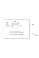
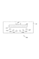
図1は、基板110をコーティングするシステム100の略図である。スパッタされた材料で基板をコーティングする本明細書に記載されたプロセスは通常、薄膜用途に関する。本明細書では用語「コーティングする」と用語「堆積させる」を同義語として使用する。本明細書で使用する用語「基板」は、(限定はされないがウエハ、ガラス板などの)不撓性の基板と(限定はされないがウエブ、箔などの)可撓性の基板の両方を包含する。
FIG. 1 is a schematic diagram of a
図1の例示的なコーティングシステムはターゲット120を含み、ターゲット120は、ターゲット120からスパッタされた材料が基板110上に堆積することができるように基板110の上方に配置されている。本明細書で使用するとき、用語「ターゲット」は、それをスパッタすることによって基板の上方に層を形成するための原料物質を含む固体を指す。典型的な実施形態によれば、ターゲット120は実質的に円筒形に形成される。あるいは、ターゲット120は、コーティングシステム100が本明細書に記載されたとおりに層を形成することを可能にする任意の形状寸法を有することができる。さらに、図6および7に示すように、複数のターゲット要素によってターゲット120を構成することもできる。用語「〜の上方に」は単に、スパッタされた材料が基板110の上に堆積することを容易にする、基板110に対するターゲット120の相対位置を指しているだけであることに留意すべきである。具体的には、用語「〜の上方に」を、垂直な上下の方向だけに限定されると理解すべきではない。用語「〜の上方に」は、コーティングシステム100が本明細書に記載されたとおりに機能することを可能にするのに適した、基板110に対するターゲット120の任意の相対位置を指すことができる。具体的には、ターゲット120と基板の両方を垂直に向けることもできる。
The exemplary coating system of FIG. 1 includes a
ターゲット120は一般に、スパッタリングを実行するためのスパッタリングシステムに関連づけられ、または、ターゲット120に関連づけられた後にさらに論じるカソードアセンブリ(図示せず)などのスパッタリングシステムの部分を形成する。例示的なシステム100などの本明細書の典型的な実施形態に基づくコーティングシステムはスパッタリング装置を構成する。典型的な実施形態によれば、マグネトロンスパッタリングとしてスパッタリングを実行することができる。あるいは、限定はされないが、スパッタリングが、ダイオードスパッタリングからなることもできる。
マグネトロンスパッタリングは、堆積速度が比較的に大きいため、特に有利なことがある。本明細書で記載された任意の実施形態と組み合わせることができる典型的な実施形態によれば(図3に関する後の説明を参照されたい)、コーティングする基板表面に面した側とは反対側のターゲット表面の近くに磁場を発生させることができるような態様で、ターゲット120に磁石が関連づけられる。それによって、発生した磁場の範囲内に自由電子を閉じ込めて、ダイオードスパッタリングと同じ程度に自由電子が自由に基板を衝撃することがないようにすることができる。同時に、自由電子は、磁場の中に閉じ込められたときに、自由電子が中性ガス分子をイオン化する確率を、ダイオードスパッタリングに比べて数桁高める。この効果によって利用可能なイオンの数が増え、それによって、ターゲット材料が侵食され、続いて基板上に堆積する速度が相当に増大することがある。
Magnetron sputtering may be particularly advantageous due to the relatively high deposition rate. According to an exemplary embodiment that can be combined with any of the embodiments described herein (see later description with respect to FIG. 3), the side opposite the side facing the substrate surface to be coated A magnet is associated with the
典型的な実施形態によれば、コーティングシステム100は真空チャンバ102を含み、スパッタリングプロセスは真空チャンバ102内で実行される。本出願内で使用する用語「真空」は、10−2ミリバールよりも低い圧力(例えば、限定はされないが、約10−2ミリバール。真空チャンバ102内に処理ガスが流れているときなどにこの圧力になることがある)、またはより具体的には10−3ミリバールよりも低い圧力(例えば、限定はされないが、約10−5ミリバール。真空チャンバ102内に処理ガスが流れていないときなどにこの圧力になることがある)を指す。コーティングシステム100は、製造システム(図示せず)の部分を形成する処理モジュールを形成することができる。例えば、コーティングシステム100は、TFT製造システム内、または、より具体的には、限定はされないがAKT−PiVot PVDシステム(Applied Materials、米カリフォルニア州Santa Clara)などのTFT−LCD製造システム内に実装することができる。
According to an exemplary embodiment, the
典型的な実施形態によれば、ターゲット120と基板110の間の相対位置を変化させる。本明細書で使用するとき、ターゲットと基板の間の相対位置を変化させることは、基板110の上方に堆積するスパッタされた材料の分布が、以前の相対位置と変化させた後の相対位置との間で実質的に変わるように、ターゲットまたは基板の配置および/または向きを変更することとして理解される。
According to an exemplary embodiment, the relative position between the
すなわち、相対位置を変化させることは、具体的には、前後に移動させること、もしくは上下に移動させること、あるいはこれらの移動の組合せを含む。本開示は通常、「静的スパッタリング」と呼ばれるものに関する。相対位置を変化させること、および基板及び1つまたは複数のターゲットのうちの少なくとも一方を移動させることを、ターゲットの前を基板が輸送方向に次々と絶え間なく移動する動的スパッタリングと取り違えてはならない。本開示は特に、基板および1つまたは複数のターゲットを、基板の輸送方向とは異なる方向に相対的に移動させることに関する。この文脈では異なる方向が、輸送方向と交差する任意の方向(例えば90°の角度で交差する方向)および輸送方向とは反対の方向を含むことができる。本開示は特に、基板および1つまたは複数のターゲットを相対的に移動させ、この移動を、選択された時間の間、停止することに関する。 That is, changing the relative position specifically includes moving back and forth, moving up and down, or a combination of these movements. The present disclosure relates to what is commonly referred to as “static sputtering”. Changing the relative position and moving at least one of the substrate and one or more targets must not be confused with dynamic sputtering where the substrate moves continuously in the direction of transport in front of the target. . In particular, the present disclosure relates to moving the substrate and one or more targets relative to a direction different from the direction of substrate transport. Different directions in this context can include any direction that intersects the transport direction (eg, a direction that intersects at an angle of 90 °) and the opposite direction to the transport direction. In particular, the present disclosure relates to relatively moving a substrate and one or more targets and stopping the movement for a selected time.
例えば、堆積するスパッタされた材料の分布が実質的に変わるように、基板110を、ターゲット120に対して変位させる(すなわち平行移動または回転させる)ことができる。具体的には、本明細書のある種の実施形態によれば、相対位置を変化させることが、(図1の基板ワブル(wobble)方向106によって示されているように)スパッタされた材料の前記層を形成する基板の表面に実質的に平行な平面に沿って、基板110を、ターゲット120に対して変位させることを含む。
For example, the
例えば、ワブル移動の外側位置に到達するために、基板110を、220mmよりも短い距離だけ、より具体的には180mmよりも短い距離だけ、さらに具体的には150mmよりも短い距離だけ変位させることができる。あるいは、ワブル移動の外側位置に到達するために、基板110を、基板の長さの10%よりも短い距離だけ、より具体的には7.5%よりも短い距離だけ、さらに具体的には5%よりも短い距離だけ変位させることもできる。具体的には、これらの百分率は、2500mm×2200mmの平面寸法を有するGen 8.5基板に対して適用することができる。
For example, to reach the outer position of the wobble movement, the
あるいは、基板110の上方に堆積するスパッタされた材料の分布が実質的に変わるように、ターゲット120を、基板110に対して変位させる(すなわち平行移動または回転させる)こともできる。具体的には、後にさらに論じる特定の実施形態によれば、ターゲット120が、往復するように回転する平面ターゲットである。(例えば回転カソード内に見られるような)実質的に円筒形のターゲットをその対称軸を軸として回転させても、回転カソードにおいてそうであるように、基板110の上方に堆積するスパッタされた材料の分布は実質的に変わらないことに留意すべきである。したがって、円筒形のターゲットをこのように回転させても、本開示内において理解されるターゲットと基板の間の相対位置の変化にはつながらない。回転カソードは、実質的に円筒形のターゲットを含みまたは実質的に円筒形のターゲットに関連づけられており、少なくともそのターゲットがその円筒対称軸を軸に回転可能である、例えばAKT−PiVot PVDシステム内で使用されているようなカソードアセンブリであると理解される。したがって、本明細書内で理解されるように、句「回転ターゲットを回転させる」は、回転ターゲットを揺動させること、すなわち、ターゲットの中心の位置が一定しないような方法で回転ターゲットを動かすことを指す。
Alternatively, the
具体的には、典型的な実施形態によれば、ターゲット120と基板110の間の相対位置を、ワブリング(wobbling)が実行されるような態様で変化させる。用語「ワブリング」は、ターゲット120と基板110の間の相対位置を、ゼロ位置(zero position)を挟んで変化させることと理解される。例えば、限定はされないが、基板110および/またはターゲット120を、左右に(すなわち2つの外側位置間を往復するように)変位させまたは回転させることができる。ターゲット120と基板110の間の相対位置は、後にさらに示すように、本明細書の実施形態に従って基板上に層を形成することを可能にする適当な移動パターンに従って変化させることができる。
Specifically, according to an exemplary embodiment, the relative position between the
本明細書の任意の実施形態と組み合わせることができる典型的な実施形態によれば、コーティングシステム100は、基板キャリア104上に配置された基板110とターゲット120との間の相対位置を変化させるように構成された駆動システムを含む。基板キャリア104は移動可能とすることができる。コーティングシステム100は、基板110を平行移動または回転させることによってターゲット120と基板110の間の相対位置を変化させる、移動可能な基板キャリア104に関連づけられた基板ワブル駆動システム108(図1に示されている)を含むことができる。例示的な実施形態では、基板ワブル駆動システム108が、基板110を、基板ワブル方向106に沿って平行移動させる。あるいは、基板ワブル駆動システム108が、基板110のコーティングされた表面に対して垂直な方向など、他の方向に沿った平行移動を実行してもよい。一般に、スパッタされた粒子の主たる移動方向(例えば図1では垂直方向)に対して垂直な平面に平行に基板110を平行移動させると有利である。あるいは、限定はされないが、ワブル駆動システム108が、限定はされないが平面対称軸などの基板110の縦軸を軸にした基板110の回転を実行してもよい。
According to an exemplary embodiment that can be combined with any embodiment herein, the
基板ワブル駆動システム108は、基板キャリア104を本明細書の実施形態に従って移動させる(具体的には基板キャリア104のワブリングを実施する)のに適した移動機構とすることができる。例えば、限定はされないが、基板ワブル駆動システム108は、駆動装置(図示せず)によって生み出された駆動力を結合する結合要素(図示せず)を含むことができる。この結合要素は駆動シャフトなどである。基板キャリア104の水平方向の(すなわちコーティングする基板の表面に平行な)平行移動を容易にするため、基板キャリア104を案内システム(例えばレール装置)に載せることができる。基板キャリア104、したがって基板110を水平方向に平行移動させることができるように、この駆動装置は、モータと、モータのトルクを直線的な駆動力に変換する手段とを含むことができる。基板表面に対して垂直な軸を軸に基板110を回転させたり、またはそのような軸に沿って平行移動させたりするなど、基板110を他の方向に沿って移動させ、またはより具体的には基板110を他の方向に沿ってワブリングさせる同様の駆動システムを配置してもよい。
The substrate
あるいは、ターゲット120の平行移動または適当な回転を達成することによってターゲット120と基板110の間の相対位置を変えるコーティングシステムのために、ターゲット120に対して働く駆動システムを配置してもよい。図2は、コーティングシステム100に対するこのような代替実施形態を概略的に示す。コーティングシステム200では、ターゲット120が、層の形成中に、ターゲットワブル方向206に沿って移動することができるように構成されている。このような実施形態では、層形成プロセスの間中、基板110が、真空チャンバ102に対して静止したままである。さらに、コーティングシステム200は、本明細書の実施形態に従ってターゲット120を移動させるように(具体的にはターゲット120をワブリングさせるように)適合されたターゲットワブル駆動システム208を含む。この例示的なシステムでは、ターゲットワブル駆動システム208が、ターゲット120を、基板ワブル方向106に沿って平行移動させる。あるいは、限定はされないが、平面ターゲットに関して後にさらに説明するように、ターゲットワブル駆動システム208が、ターゲット120の縦軸を軸としたターゲット120の回転を実施してもよい。ターゲットワブル駆動システム208は(基板ワブル駆動システム108と同様に)、ターゲット120の移動を生じさせることによってターゲット−基板相対位置を適当に変化させる適当な駆動システム(図示せず)を含むことができる。
Alternatively, a drive system that acts on the
ある種の実施形態によれば、ターゲットから材料を基板110の上方にスパッタすることは、(a)ターゲット120と基板110の間の相対位置を第1の位置Iへ変化させ、この相対位置を、第1の位置Iに維持すること、および(b)ターゲット120と基板220の間の相対位置を第2の位置IIへ変化させることを含む。典型的な実施形態によれば、これらの相対位置を、選択された時間間隔の間、維持する。すなわち、第1の位置を、所定の第1の時間間隔の間、維持し、第2の位置を、所定の第2の時間間隔の間、維持する。第1の位置Iおよび第2の位置IIをそれぞれ、基板110とターゲット120の間の相対位置の変化に帰着するワブリング変位の外側位置に対応させることができる。
According to certain embodiments, sputtering material from the target onto the
本明細書の任意の実施形態と組み合わせることができるある種の実施形態によれば、この所定の第1の時間間隔が少なくとも0.1秒、好ましくは少なくとも0.5秒、さらに好ましくは少なくとも1秒である。これらの所定の時間間隔を、少なくとも10秒など、より長くすることも可能であり、または、少なくとも30秒など、さらに長くすることも可能である。具体的には、この相対位置を、層形成プロセスの総時間または総スパッタリング時間のうちの所定の百分率の間、例えば総層形成プロセスの総時間または総スパッタリング時間の少なくとも40%、より具体的には少なくとも20%、さらに具体的には少なくとも10%の間、またはこれらの百分率の間の時間間隔、例えば40から10%、40から20%、20から10%などの間、外側位置(すなわち第1および第2の位置)に維持することができる。 According to certain embodiments that can be combined with any embodiment herein, this predetermined first time interval is at least 0.1 seconds, preferably at least 0.5 seconds, more preferably at least 1 Seconds. These predetermined time intervals can be longer, such as at least 10 seconds, or even longer, such as at least 30 seconds. Specifically, this relative position may be a predetermined percentage of the total time of the layer formation process or the total sputtering time, such as at least 40% of the total time of the total layer formation process or the total sputtering time, more specifically. Is at least 20%, more specifically at least 10%, or a time interval between these percentages, eg 40 to 10%, 40 to 20%, 20 to 10%, etc. 1 and 2 positions).
この層形成プロセスは、材料がスパッタされている処理時間と、材料がスパッタされていない処理時間(例えば、ターゲットから材料がスパッタされないターゲット−基板相対位置の変化中など、1つの層の形成中の2つのスパッタリング間隔とスパッタリング間隔の間の時間)とを含むことに留意すべきである。層形成プロセス中にターゲット120と基板110の間の相対位置が固定される、第1の位置、第2の位置などの位置にあるときにだけ、スパッタリングを実行してもよい。その場合、相対位置を外側位置に維持することができる時間の総スパッタリング時間に対する所定の百分率は、約100%である。それによって特に高い均一性を達成することができる。
This layer formation process involves the processing time during which the material is sputtered and the processing time during which the material is not sputtered (e.g., during a change in target-substrate relative position where no material is sputtered from the target). It should be noted that the two sputtering intervals and the time between the sputtering intervals). Sputtering may be performed only when the relative position between the
本開示の実施形態によれば、層形成プロセス中に、基板110および/またはターゲット120を第1の相対位置に変位させ、その位置を、所定の第1の時間の間、維持する。この第1の相対位置は図1および2の位置Iに対応する。次いで、基板110および/またはターゲット120を第2の相対位置(図1および2の位置II)に変位させ、その位置を、所定の第2の時間の間、維持する。相対位置をこのような変位させると、基板110の上方にスパッタされた材料の分布が非対称になる可能性がある。このような非対称分布の結果、コーティング室内の基板ホルダ、壁などのコーティングを必要としないエリアのコーティング率がより高くなる可能性があり、それによってプロセス効率が低下する可能性がある。しかしながら、驚くべきことに、この状況にもかかわらず、それによって基板上に堆積する層の均質性が、プロセスの間、基板とターゲットの間の相対位置が不変である層形成プロセスよりも高くなることがあることを、本開示の発明者は見出した。この文脈では、層の均質性が一般に、基板上のコーティングされたエリア全体にわたる層の厚さ、結晶構造、抵抗率および/または層応力の均一性を指すことに留意すべきである。
According to embodiments of the present disclosure, during the layer formation process, the
いくつかの実施形態によれば、ターゲット120は回転ターゲットであり、より具体的には、その円筒対称軸を軸に回転可能な実質的に円筒形のターゲットである。代替実施形態によれば、ターゲット120が平面ターゲット(すなわちスパッタされるように適合された実質的に平面のターゲット表面を有するターゲット)である。このような平面ターゲットは通常、図5に関して後にさらに示すように、平面カソードアセンブリに関連づけられる(すなわち平面カソードアセンブリの一部を形成する)。このような代替実施形態では、平面ターゲット120を往復するように回転させることによって、ターゲット120と基板110の間の相対位置を変化させる。具体的には、平面ターゲット120の縦軸、すなわちスパッタされるターゲット表面に実質的に平行なターゲット本体を横断する軸を軸に平面ターゲット120を回転させる。平面ターゲットに関する実施形態の詳細については後にさらに論じる(図5および7に関する説明を参照されたい)。
According to some embodiments, the
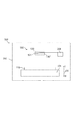
図3は、本明細書に記載された実施形態で使用されるカソードアセンブリ310をより詳細に例示する。図3に示された要素は全て、本明細書に記載された実施形態のうちの少なくともいくつかの実施形態、特に図1および2に関して説明した実施形態と組み合わせることもできることを理解すべきである。図3は、バッキング管330上に配置された円筒形の回転ターゲット120’を示す。具体的には、限定はされないが、円筒形の回転ターゲット120’はバッキング管330に接着することができる。ターゲット120’の材料は通常、スパッタリング中のターゲット120’がその円筒対称軸を軸に回転している間に消散する。ある種の実施形態によれば、スパッタリングプロセスによって生じる可能性があるターゲット上の高温を低下させるために、カソードアセンブリ310が冷却システム340を含む。冷却システム340は例えば、限定はされないが、水などの冷却材または他の適当な冷却材を含む管によって構成することができる。冷却すると有利になりうるのは、通常は数キロワット程度であるスパッタリングプロセスに投入されるエネルギーの大部分が熱に転化され、その熱がターゲットに伝達される可能性があるためである。ある種の状況では、このような熱がターゲットを傷つける。他の実施形態によれば、カソードアセンブリ310の内部を適当な冷却材で完全に満たす。
FIG. 3 illustrates in greater detail the
図3の略図に示されているように、カソードアセンブリ310は磁石アセンブリ325を含むことができる。この例示的な実施形態では、磁石アセンブリ325がバッキング管330内に配置される。本明細書の実施形態によれば、カソードアセンブリは、バッキング管330内に、2つ、3つまたは4つ以上などの適当な数の磁石アセンブリを含むことができる。カソードアセンブリ310は、駆動システム(図示せず)に関連づけられて、バッキング管330の回転、したがってターゲット120’の回転を少なくとも実行するシャフト321を含むことができる。この例示的な実施形態では、シャフト321の位置がターゲット120’の円筒対称軸に対応する。それによって、本明細書の実施形態に基づくコーティングシステム内に回転ターゲットを実装することができ、それによって、ターゲット材料のより高度な利用を容易にすることができる。この例示的な実施形態では、基板110上におけるスパッタされた材料の非常に均一な層の形成を容易にするため、スパッタリングターゲット120’のこの回転を、基板110の水平方向の平行移動と組み合わせる。あるいは、スパッタリングターゲット120’の回転を、ターゲット120’と基板110の間の相対位置を変化させるのに適した本明細書の実施形態に基づく他の方法、例えば、限定はされないが、カソードアセンブリ310全体のワブリングと組み合わせることもできる。
As shown in the schematic diagram of FIG. 3, the
本開示の一態様によれば、スパッタされた材料の層を基板の上方に形成する間に、ターゲットに関連づけられたカソードアセンブリに印加する電圧を時間の経過に従って変化させる。言い換えると、スパッタリング中のカソードアセンブリに一定でない電圧を印加することができる。重要には、スパッタ力は通常、カソードアセンブリに印加された電圧に直接に対応している。0Vに近い値を除けば、印加電圧とスパッタ力の間の関係はほぼ直線的である。したがって、ある種の実施形態によれば、基板110とターゲット120’の間の相対位置に応じてスパッタ力を変える。
According to one aspect of the present disclosure, the voltage applied to the cathode assembly associated with the target is varied over time while a layer of sputtered material is formed over the substrate. In other words, a non-constant voltage can be applied to the cathode assembly during sputtering. Importantly, the sputtering force typically corresponds directly to the voltage applied to the cathode assembly. Except for values close to 0V, the relationship between applied voltage and sputtering force is almost linear. Thus, according to certain embodiments, the sputtering force is varied depending on the relative position between the
図3に示した例示的な実施形態では、電圧供給源312が、(ターゲット120’に関連づけられた)カソードアセンブリ310に電圧を印加する。具体的には、バッキング管330に負電位を印加するために、電気接続314によって電圧供給源312をバッキング管330に電気的に接続することができる。バッキング管330は、バッキング管330が電極として機能することができるような適当な材料から構成される。そのような適当な材料は金属、例えば、限定はされないが、銅とすることができる。ある種の実施形態によれば、スパッタプロセスを容易にするために、ターゲット120’の近くに正電極(すなわちスパッタリングの間、正電位を有することができる電極。アノードとも呼ばれる)が配置される。
In the exemplary embodiment shown in FIG. 3,
したがって、本明細書の実施形態によれば、カソードアセンブリ310に電圧を印加することによって、ターゲット、例えば、限定はされないが、例示的なターゲット120および120’に、電場を関連づけることができる。
Thus, according to embodiments herein, an electric field can be associated with targets, eg, but not limited to,
ターゲット−基板相対位置が前述の第1および第2の位置に留まる時間の長さによって、本明細書の実施形態に従って形成される層の均一性がさらに向上する場合があることに本発明の発明者は気づいた。具体的には、総処理時間に対して、ターゲット−基板相対位置が第1および第2の位置に留まる時間が長いほど、均質性、特に均一性は良好になる。したがって、第1および第2の位置でスパッタリングを実行することによって均質性を最大にすることができる。移動時(すなわちターゲット−基板相対位置を変化させているとき)にスパッタリング電場をオフにすることも可能であり、それによって均一性をさらに増大させることができる。 The invention of the present invention that the length of time that the target-substrate relative position remains at the first and second positions described above may further improve the uniformity of the layer formed according to the embodiments herein. Noticed. Specifically, the longer the time during which the target-substrate relative position stays at the first and second positions with respect to the total processing time, the better the homogeneity, particularly the uniformity. Thus, homogeneity can be maximized by performing sputtering at the first and second positions. It is also possible to turn off the sputtering electric field during movement (ie when changing the target-substrate relative position), thereby further increasing the uniformity.
具体的には、相対位置を変化させているときに電場を弱くしまたはオフにした場合には、層の均質性をさらに増大させることができることを本開示の発明者は見出した。より具体的には、基板とターゲットの間の相対位置がワブリングの外側位置に対応していないときにスパッタリングを中断した場合には、均質性を増大させることができる。スパッタリングの中断は、ターゲットに関連づけられたカソードアセンブリと関連アノードとの間の電位差をゼロに近い値またはゼロにセットすることによって達成することができる。 Specifically, the inventors of the present disclosure have found that layer homogeneity can be further increased if the electric field is weakened or turned off while changing the relative position. More specifically, homogeneity can be increased if sputtering is interrupted when the relative position between the substrate and the target does not correspond to the outer position of the wobbling. The interruption of sputtering can be achieved by setting the potential difference between the cathode assembly associated with the target and the associated anode to a value close to zero or zero.
したがって、ある種の実施形態によれば、前記相対位置を変化させることが、前述の相対位置を第1の位置から第2の位置へ変化させることを含み、ターゲット120に関連づけられたカソードアセンブリ310に印加する電圧は、相対位置が第1または第2の位置に対応するときの方が、相対位置が前記第1の位置と前記第2の位置の間の位置に対応するときよりも高い。具体的には、前記相対位置が第1の位置と第2の位置の間の位置に対応するときに、この電圧を実質的にゼロにすることができる。より具体的には、前記相対位置を変化させている間に、この電圧を、時間の経過とともに、方形波の波形に従って変化させることができる。
Thus, according to certain embodiments, changing the relative position includes changing the relative position from a first position to a second position, and includes a
図4は、アノードとカソードアセンブリの間に印加する電圧Vが一定ではなく方形波の形状を有する実施形態における電圧Vを示す。この図に示されているように、この電圧は、ある時間の間、ゼロでないある一定のレベルに維持される。この時間は通常、第1または第2のスパッタリング間隔(すなわち相対位置が不変である時間)である。次いで、ある時間間隔においてこの電圧を大幅に引き下げる。これらの時間間隔は通常、相対位置を変化させている時間、例えば前述の第1の位置から第2の位置へ相対位置を変えている時間に対応する。 FIG. 4 shows the voltage V in an embodiment where the voltage V applied between the anode and cathode assembly is not constant but has a square wave shape. As shown in this figure, this voltage is maintained at a certain non-zero level for a period of time. This time is typically the first or second sputtering interval (i.e., the time during which the relative position remains unchanged). This voltage is then significantly reduced at certain time intervals. These time intervals usually correspond to the time for changing the relative position, for example, the time for changing the relative position from the first position to the second position.
ある種の実施形態によれば、電圧を大幅に引き下げるときに電圧を0Vにする。それによってスパッタリングはほぼ瞬時に停止する。代替実施形態によれば、スパッタリングプロセスの初期電圧として適当と思われるあるしきい値まで電圧を引き下げる。例えば、このようなしきい電圧はスパッタリングを停止することができるが、スパッタプロセスの再開をより容易にすることができる。しかしながら、基板110とターゲット120の間の相対位置を変えているときに、この電圧を、スパッタ電圧の10%(より典型的にはスパッタ電圧の5%)よりも小さい値まで引き下げることができる。
According to certain embodiments, the voltage is brought to 0V when the voltage is significantly reduced. Thereby, the sputtering stops almost instantaneously. According to an alternative embodiment, the voltage is reduced to a certain threshold that may be appropriate as an initial voltage for the sputtering process. For example, such a threshold voltage can stop sputtering, but can make it easier to resume the sputtering process. However, when changing the relative position between the
前述のとおり、スパッタリング中のカソードアセンブリ310に一定でない電圧を印加することができる。典型的な実施形態によれば、この電圧を、ターゲット120と基板110の間の相対位置と同期させる。例えば、カソードアセンブリを移動させている間、この電圧を、カソードアセンブリ310に印加する最大電圧値の35%よりも小さい値、より具体的には20%よりも小さい値にセットすることができる。図10は、時間tの経過とともに正弦波の形状に従って変化する電圧Vを例示的に示す。相対位置を正弦波電圧Vと同期させることができる。例えば、限定はされないが、電圧Vが、図10に示された点線よりも大きい(すなわち図10に示された点線よりも上にある)ときには、相対位置を不変にすることができる。電圧Vが点線よりも小さい(すなわち点線よりも下にある)時間の間に、相対位置を、第1の位置から第2の位置へ、続いて第2の位置から第1の位置へ交互に変化させることができる。
As described above, a non-constant voltage can be applied to the
本明細書の他の実施形態と組み合わせることができるある種の実施形態によれば、全形成プロセスの間に1度だけ、相対位置を第1の位置から第2の位置へ変化させる。代替実施形態によれば、相対位置を第1の位置から第2の位置へ変化させ、続いて第2の位置から第1の位置へ変化させる。全形成プロセスの間に、このような一連の移動を複数回繰り返すことができる。例えば、相対位置を3回以上変えて、基板をコーティングするときに相対位置が第1および第2の位置にそれぞれ2回以上対応するようにすることができる。このような移動パターンは、この一連の移動を実施し、その間にスパッタリング力を変化させるのに時間を要するため、総処理時間を増大させると思われるが、このような移動パターンの結果、層の均質性をさらに増大させることができる。 According to certain embodiments that can be combined with other embodiments herein, the relative position is changed from the first position to the second position only once during the entire formation process. According to an alternative embodiment, the relative position is changed from the first position to the second position and subsequently changed from the second position to the first position. Such a series of movements can be repeated multiple times during the entire forming process. For example, the relative position can be changed three or more times so that the relative position corresponds to the first and second positions two or more times when the substrate is coated. Such a movement pattern is likely to increase the total processing time because it takes time to perform this series of movements, during which the sputtering force is changed, but as a result of such a movement pattern, the layer The homogeneity can be further increased.
ある種の実施形態によれば、スパッタされた材料の層を形成することが、(i)基板110とターゲット120の間の相対位置を第1の位置に維持し、その間、スパッタリングのための電場をオンにすること、(ii)第1の時間間隔が経過した後、基板110とターゲット120の間の相対位置を、(例えば図1に示したように基板110を変位させることによって、または図2に示したようにターゲット120を変位させることによって)第2の位置にセットし、第1の位置から第2の位置へ相対位置を変形させている間は電場をオフにすること、および(iii)基板110とターゲット120の間の相対位置を、第2の時間間隔の間、第2の位置に維持し、その間、電場をオンにすることを含む。その後に、ステップ(ii)および(i)をこの順番で同様に実行いて、相対位置を第2の位置から第1の位置へ変化させることができる。句「電場をオンにする」は、ターゲット120に関連づけられたカソードアセンブリおよびカソードアセンブリに関連づけられたアノードに電圧を印加することと理解される。典型的な実施形態によれば、第1の時間間隔および/または第2の時間間隔の間、印加電圧が一定である。印加電圧は、相対位置が第1の位置に対応している時間と相対位置が第2の位置に対応している時間とで等しくすることができる。
According to certain embodiments, forming a layer of sputtered material (i) maintains a relative position between the
図5および7に示すある種の実施形態によれば、基板をコーティングするシステムであって、材料を基板上にスパッタするための1つまたは複数の平面ターゲットを含むコーティングシステムが提供される。これらの実施形態の少なくとも1つの平面ターゲットは、前記基板のコーティング中に往復するように回転可能である。本明細書で使用する用語「往復するように回転可能である」は、往復運動、すなわち平面ターゲットを第1の位置まで回転させ、次いで第1の位置から逆方向に第2の位置まで回転させる運動に従って回転可能であると理解すべきである。第1の位置および第2の位置を、平面ターゲットの回転の外側位置とも呼ぶ。ある種の実施形態によれば、スパッタリングを容易にするため、平面ターゲットが平面カソードアセンブリに関連づけられる。平面ターゲットの回転は、カソードアセンブリ全体を回転させることによって実施することができる。特定の実施形態によれば、平面ターゲットが、基板表面に平行な軸、具体的には平面ターゲット(または平面ターゲットに関連づけられた平面カソード)の縦軸、より具体的には平面ターゲット(または平面ターゲットに関連づけられた平面カソード)の中心軸を軸に回転可能である。 According to certain embodiments shown in FIGS. 5 and 7, a system for coating a substrate is provided that includes one or more planar targets for sputtering material onto the substrate. At least one planar target of these embodiments is rotatable to reciprocate during the coating of the substrate. As used herein, the term “rotable to reciprocate” means reciprocating motion, ie, rotating a planar target to a first position and then rotating from the first position to the second position in the reverse direction. It should be understood that it can rotate according to movement. The first position and the second position are also referred to as outer positions of the planar target rotation. According to certain embodiments, a planar target is associated with the planar cathode assembly to facilitate sputtering. The rotation of the planar target can be performed by rotating the entire cathode assembly. According to certain embodiments, the planar target is an axis parallel to the substrate surface, specifically the longitudinal axis of the planar target (or planar cathode associated with the planar target), more specifically the planar target (or planar). It can be rotated about the central axis of the flat cathode associated with the target.
図5は、平面ターゲット120”に関連づけられた平面カソードアセンブリ502を含む例示的な他のコーティングシステム500を示す。図5に示された要素は全て、本明細書に記載された実施形態のうちの少なくともいくつかの実施形態、特に図1および2に関して説明した実施形態と組み合わせることもできることを理解すべきである。平面カソードアセンブリ502は、平面ターゲット120の支持を提供する平面バッキング体530を含む。具体的には、平面ターゲット120”は平面バッキング体530に接着することができる。バッキング体530が(バッキング管330に関して上で説明したのと同様の方法で)電極として機能するように、平面バッキング体530を電圧源(この図には示されていない)に接続することができる。本明細書に記載されたターゲット120”からのスパッタリングを生じさせるのに適した電場を発生させるため、カソードアセンブリ502をアノード(図示せず)に関連づけることができる。平面カソードアセンブリ502は、限定はされないが、マグネトロンスパッタリング用の磁石アセンブリおよび/または本明細書に記載された冷却システムなど、図5に示されていない他の要素を含むことができる。
FIG. 5 illustrates another
基板110のコーティング中に、平面ターゲット120”は、平面ターゲット120”と基板110の間の相対位置が変化するような態様で、往復するように回転可能である。具体的には、ピボット回転軸504を軸に平面ターゲット120”を回転させることができる。この例示的な実施形態では、ピボット回転軸504が、平面カソードアセンブリ502の中心軸に対応する。本明細書の実施形態によれば、ピボット回転軸504を、コーティングする基板110の表面に平行な軸、例えば、限定はされないが、ターゲット120”の縦軸に対応させることができる。具体的には、ピボット回転軸504を、カソードアセンブリ502またはターゲットアセンブリ120”の中線からずらすことができる。一般に、対応する回転が、ターゲット120”と基板110の間の相対位置を変化させるものである限り、ピボット回転軸504はどの軸に対応するものであってもよい。
During coating of the
図5には、相対位置を変化させるために平面ターゲット120”を回転させることができる角度βおよび−βが示されている。角度βは、平面ターゲット120”に垂直な軸と基板110に垂直な軸512とによって形成される角度である。線508および510は、その外側位置にある平面ターゲット120”に垂直な軸を示す。この角度の値は、ターゲット120”の時計回りの回転に対して正、ターゲット120”の反時計回りの回転に対して負である。コーティングする基板110の表面に平行に平面ターゲット120”が配置されているとき、この角度の値はゼロに対応する。したがって、ターゲット120”の外側位置(すなわち前述の第1および第2の位置)における平面ターゲットの角度βはゼロでないある値(以後、非ゼロ値)に対応する。この例示的な実施形態では、この角度の絶対値が、ターゲットの両方の外側位置(すなわち前述の第1および第2の位置)で同じである。あるいは、一方の外側位置ともう一方の外側位置とでこの角度の絶対値が異なっていてもよい。典型的な実施形態によれば、この角度の絶対値が50度未満、より具体的には45度未満、さらに具体的には30度未満である。
FIG. 5 shows angles β and −β by which the
典型的な実施形態によれば、ターゲット120”の回転は、ピボット回転軸504の位置に配置されたシャフト(図示せず)によって達成することができる。ターゲット120”の往復回転を生み出すため、このようなシャフトをターゲットワブル駆動システム208に結合することができる。例えば、限定はされないが、ターゲットワブル駆動システム208は、ターゲット120”の往復動回転が生み出されるように、電気機械式モータ(図示せず)と、モータによって生み出されたトルクをピボット回転軸504に結合するシャフト(図示せず)とを含むことができる。
According to an exemplary embodiment, rotation of the
コーティングシステム500(このシステムだけに限定されるわけではない)に関連したある種の実施形態によれば、基板110をコーティングする方法が提供される。この方法は、スパッタされた材料の層を前記基板110上に形成することを含み、スパッタされた材料の層を形成することは、平面ターゲット120”から材料を基板110の上方にスパッタすること、および平面ターゲット120”を往復するように回転させることによって、ターゲット120”と基板110の間の相対位置を変化させることを含む。
According to certain embodiments associated with the coating system 500 (not limited to this system), a method of coating the
これらの最後の実施形態は、ターゲット120”と基板110の間の相対位置を、適当な回転パターンに従って変化させることができる。例えば、平面ターゲットを一定の角速度で回転させることができる。あるいは、この回転を、一定でない角速度で実施することもできる。さらに、この往復回転は、外側位置における不動時間なしで実施することができる。代替実施形態によれば、平面ターゲット120”を回転させることが、ターゲット120”を第1の位置まで回転させ、この第1の位置を、所定の第1の時間間隔の間、維持すること、および、上記の方法と同様の方法で、前記ターゲットを第2の位置まで回転させ、この第2の位置を、所定の第2の時間間隔の間、維持することを含む。一般に、この第1および第2の位置は、平面ターゲット120”の往復回転の外側位置に対応させることができる。
These last embodiments can change the relative position between the
コーティングシステム500(このシステムだけに限定されるわけではない)に関連したある種の実施形態によれば、コーティングすることが、平面ターゲット120”に電圧を印加し、その電圧を、コーティング中に、時間の経過に従って変化させることを含む。より具体的には、コーティングシステム500内での相対位置の変更を、前述の電圧変化と組み合わせることができる。
According to certain embodiments associated with the coating system 500 (not limited to this system only), the coating applies a voltage to the
本明細書の任意の実施形態と組み合わせることができる典型的な実施形態によれば、ターゲット120、120’または120”が、複数のターゲット要素(すなわちターゲットアレイ)によって構成され、それらの複数のターゲット要素は、ターゲット要素からスパッタされた材料を基板110上に堆積させることができるように、空間的に離隔されて基板110の前に配置される。具体的には、ターゲット要素をそれぞれカソードアセンブリに関連づけることができ、またはそれぞれのターゲット要素がカソードアセンブリの部分を形成してもよい。より具体的には、それらの複数のカソードアセンブリを、カソードアセンブリのアレイとして配置することができる。特に、大面積基板の静的な堆積では、規則正しく配置されたカソードアセンブリの1次元アレイを使用することが一般的である。処理チャンバ内のカソードアセンブリ(および関連ターゲット)の数は、典型的には2つから20個の間、より典型的には9つから16個の間である。
According to an exemplary embodiment that can be combined with any embodiment herein, a
アレイ実施形態によれば、複数のターゲット要素を同期させて平行移動させまたは適当に回転させることによって、ターゲット要素と基板110の間の相対位置を変化させることができる。あるいは、ターゲットアレイに対して基板110を変位させることによって相対位置を変化させることもできる。一般に、複数のターゲットと基板の間の相対位置は、コーティングシステムが本明細書の実施形態に従って機能することを可能にする適当な方法で変化させることができる。一般に、ターゲット要素の同期変位は、堆積する層の均質性をさらに増大させる。
According to the array embodiment, the relative position between the target element and the
特定の実施形態に限定されることなく、カソードアセンブリは一般に、互いに等間隔に配置することができる。具体的には、ターゲットはターゲット要素のアレイを含むことができる。さらに、ターゲットの長さを、コーティングする基板の長さよりもわずかに長くすることができる。それに加えてまたはその代わりに、カソードアレイは、基板の幅よりもわずかに広い距離にわたって延びる。「わずかに」は通常、100%から110%の間の範囲を含む。わずかに大きなコーティング長さ/幅の使用は、コーティング中の境界効果の回避を容易にする。複数のカソードアセンブリは、基板110から等距離のところに配置することができる。
Without being limited to a particular embodiment, the cathode assemblies can generally be equally spaced from one another. Specifically, the target can include an array of target elements. Furthermore, the length of the target can be slightly longer than the length of the substrate to be coated. In addition or alternatively, the cathode array extends over a distance slightly greater than the width of the substrate. “Slightly” usually includes a range between 100% and 110%. The use of a slightly larger coating length / width facilitates avoidance of boundary effects during coating. The plurality of cathode assemblies can be located equidistant from the
ある種の実施形態によれば、複数のカソードアセンブリを、基板110から等距離のところに配置するのではなしに、円弧形に沿って配置する。この円弧形は、内側のカソードアセンブリの方が外側のカソードアセンブリよりも基板110の近くに配置されるような形状とすることができる。この円弧形は、図6に概略的に示されているように、外側のカソードアセンブリが内側のカソードアセンブリよりも基板110の近くに位置するような形状とすることができる。あるいは、この円弧形を、内側のカソードアセンブリが外側のカソードアセンブリよりも基板の近くに位置するような形状とすることもできる。散乱挙動は一般に、スパッタされる材料に依存する。したがって、用途によっては、すなわちスパッタする材料によっては、カソードアセンブリを円弧形に配置すると、形成される層の均質性がさらに増大する。円弧の向きは一般に具体的な用途に依存する。
According to certain embodiments, the plurality of cathode assemblies are arranged along an arc instead of being arranged equidistant from the
図6は、ターゲット要素120a’から120f’を含むターゲットアレイと基板110との間の相対位置の変化が、基板ワブル方向106に沿った基板110の水平方向の平行移動(具体的には基板110のワブリング)によって達成される、例示的なコーティングシステム600を示す。この例示的な実施形態では、ターゲット要素120a’から120f’が円筒形の回転ターゲットである。代替実施形態では、ターゲット要素が適当な任意の形状を有する。
FIG. 6 shows that the relative position change between the target array including the
図7は、平面ターゲット120a”から120d”のアレイ120”を含む例示的な別のコーティングシステム700を示す。平面ターゲット120a”から120d”はそれぞれ、図5に示した平面ターゲット120”と同様に構成することができる。したがって、例示的なコーティングシステム700では、平面ターゲット120a”から120d”のアレイと基板110との間の相対位置の変化が、対応するそれぞれのピボット回転軸504を軸にしたピボット回転方向506のターゲットの同期往復回転によって達成される。図5に関して上で説明したのと同様に、平面ターゲット120a”から120d”はそれぞれ角度βだけ回転させることができる。この図では、それぞれの平面ターゲット120a”から120d”の一方の外側位置が太線の平面ターゲットによって示されており、もう一方の外側位置が細線の平面ターゲットによって示されている。図7に示されているように、基板のワブリングとターゲットのワブリングとを組み合わせて、ターゲット−基板相対変位を実行することができる。
FIG. 7 illustrates another
本開示の他の実施形態(具体的には、限定はされないが、図6および7に示した実施形態などの多数のカソードアセンブリを使用する実施形態)と組み合わせることができる特定の実施形態によれば、少なくとも1つのターゲットから材料をスパッタすることが、実質的に相補的な少なくとも2つの膜分布を重ね合わせることを含む。具体的には、本明細書に記載された実施形態は、スパッタされた材料の層の形成によって実質的に相補的な2つの膜分布が重なり合うように第1の位置および第2の位置を選択することを含む。「相補的な膜分布」は、あるターゲット−基板相対位置においてスパッタされ堆積する材料の極大厚さ領域(第1の極大)が、別のターゲット−基板相対位置においてスパッタされ堆積する材料の2つの極大厚さ領域(第2の極大)間に位置するように、第1の極大が分布することを意味する。より具体的には、堆積させた層の極大厚さを有する領域が等間隔に並ぶように、第1および第2の極大を分布させることができる。それによって、非常に均一な層の形成が容易になる。 According to certain embodiments that can be combined with other embodiments of the present disclosure (specifically, but not limited to embodiments using multiple cathode assemblies such as those shown in FIGS. 6 and 7). For example, sputtering material from at least one target includes superimposing at least two film distributions that are substantially complementary. Specifically, the embodiments described herein select the first position and the second position such that two substantially complementary film distributions overlap by the formation of a layer of sputtered material. Including doing. A “complementary film distribution” means that the maximum thickness region (first maximum) of material sputtered and deposited at one target-substrate relative position is two of the materials sputtered and deposited at another target-substrate relative position. It means that the first maximum is distributed so as to be located between the maximum thickness regions (second maximum). More specifically, the first and second maximums can be distributed so that regions having the maximum thickness of the deposited layers are arranged at equal intervals. This facilitates the formation of a very uniform layer.
具体的には、本明細書の実施形態によれば、少なくとも1つのターゲットから材料をスパッタすることが、基板の長さに沿って周期長λ(図8に示されている)で周期的に変化する厚さを有する少なくとも2つの膜分布を重ね合わせることを含む。ある種の実施形態によれば、ターゲット−基板相対位置を変化させることが、少なくとも2つの膜分布の位相が互いに異なるように実行される。例えば、周期的に変化する少なくとも2つの膜分布の位相をπ/2またはそれよりも小さい値だけずらすことができる。 Specifically, according to embodiments herein, sputtering material from at least one target is periodic with a periodic length λ (shown in FIG. 8) along the length of the substrate. Superimposing at least two film distributions having varying thicknesses. According to certain embodiments, changing the target-substrate relative position is performed such that the phases of the at least two film distributions are different from each other. For example, the phase of at least two film distributions that change periodically can be shifted by a value of π / 2 or smaller.
図8は、実質的に相補的な2つの膜分布を重ね合わせる一実施形態を示す。y軸は、膜の高さの計量単位を表し、x軸は、基板の長さの計量単位を表す。この堆積は、カソードアセンブリのアレイによって、それぞれのカソードアセンブリの堆積設定の結果、実質的に正弦波の形状の膜分布が得られるように実施される。これらの2つの堆積プロファイルは、2つの異なる位置でのスパッタリングによって得られたプロファイルである。この例では、第1の膜分布802が、第1のターゲット−基板相対位置において形成されたものである。この例では、ターゲットと基板の間の相対位置を、第2のターゲット−基板相対位置へ変化させる。
FIG. 8 illustrates one embodiment of superimposing two substantially complementary membrane distributions. The y-axis represents the unit of measurement of the film height, and the x-axis represents the unit of measurement of the substrate length. This deposition is performed by the array of cathode assemblies such that the deposition setting for each cathode assembly results in a substantially sinusoidal film distribution. These two deposition profiles are profiles obtained by sputtering at two different locations. In this example, the
相対位置は、本明細書の任意の実施形態に従って変化させることができる。例えば、前述のとおり、基板を水平方向に沿って平行移動させてもよく、あるいはターゲット(もしくはターゲットアレイ)を平行移動させまたは適当に回転させてもよい。第2のターゲット−基板位置で、第2の膜分布804を、本明細書の実施形態に従って形成する。両方の膜分布の重ね合わせにより、第1および第2の膜分布よりも高い均一性を有する層806が得られる。図8に示した略図では、膜の厚さおよび基板の長さ(X)が任意の単位(arbitrary unit)(a.u.)で示されていることに留意すべきである。
The relative position can be varied according to any embodiment herein. For example, as described above, the substrate may be translated along the horizontal direction, or the target (or target array) may be translated or appropriately rotated. At the second target-substrate location, a
ある種の実施形態によれば、層形成中に、ターゲットと基板の間の相対位置を、前述の第1および第2の位置とは別の位置において、所定の時間の間、固定することができる。それによって、層の均一性をさらに高めることができる。このような追加の位置は、第1の位置と第2の位置の間に配置される。例えば、相対位置を、所定の第3の時間(すなわち第3の時間間隔)の間、第3の位置に配置することができ、または、相対位置を、所定の第4の時間(すなわち第4の時間間隔)の間、第4の位置に配置することができる。層形成中に、相対位置を、さらに別の位置において固定することもできる。 According to certain embodiments, during layer formation, the relative position between the target and the substrate may be fixed for a predetermined time at a position different from the first and second positions described above. it can. Thereby, the uniformity of the layer can be further increased. Such an additional position is disposed between the first position and the second position. For example, the relative position can be placed at a third position for a predetermined third time (ie, a third time interval), or the relative position can be set at a predetermined fourth time (ie, a fourth time). In the fourth time interval). During the layer formation, the relative position can also be fixed at a further position.
このような追加の位置は、堆積する層の均質性の程度をより高めることを容易にすることを本出願の発明者は見出した。具体的には、スパッタされた材料の層を形成することが、複数の副層(sub−layer)を重ね合わせることを含むことができ、それぞれの副層は、所定のターゲット−基板相対位置において所定のスパッタリング電圧で堆積させる。例えば、(図7に示したような)平面ターゲット要素のアレイによってそれぞれの副層を堆積させることができ、このとき、それぞれのターゲット要素は、コーティングする基板の表面に垂直な軸に対して角度βを形成する。 The inventors of the present application have found that such an additional position makes it easier to increase the degree of homogeneity of the deposited layer. Specifically, forming a layer of sputtered material can include superimposing a plurality of sub-layers, each sub-layer at a predetermined target-substrate relative position. Deposition is performed at a predetermined sputtering voltage. For example, each sublayer can be deposited by an array of planar target elements (as shown in FIG. 7), where each target element is angled relative to an axis perpendicular to the surface of the substrate to be coated. β is formed.
この最後の実施形態では、平面ターゲットの処理力および角度を増大させると、アークの発生が非直線的に増加することに本発明の発明者は気づいた。このような実施形態では、それぞれ特定の電圧および特定の角度で堆積させたいくつかの副層(例えば4つの副層)を重ね合わせることによって、高度な均一性を得ることができることを本発明の発明者は見出した。例えば、いくつかの副層を重ね合わせることによって高い均一性を得ることができ、大きい角度でスパッタリングした副層は低いスパッタリング電圧に対応し、小さい角度でスパッタリングしたい副層は高いスパッタリング電圧に対応する。それによって、高スループット時間および層均一性を最適化することができる。 In this last embodiment, the inventors of the present invention have found that increasing the processing power and angle of the planar target increases the arc generation non-linearly. In such an embodiment, it is possible to obtain a high degree of uniformity by overlaying several sublayers (eg, four sublayers) each deposited at a specific voltage and a specific angle. The inventor found out. For example, high uniformity can be obtained by overlaying several sublayers, sublayers sputtered at large angles correspond to low sputtering voltages, and sublayers that are sputtered at small angles correspond to high sputtering voltages. . Thereby, high throughput times and layer uniformity can be optimized.
一実施形態によれば、(例えば図7のターゲット要素が角度β1を形成する)第1のターゲット−基板相対位置において、スパッタリング電圧を、所定の第1の時間間隔の間、第1の電圧値にセットして、第1の堆積ステップを実行する。続いて第2の堆積ステップを実行する。このステップでは、ターゲット−基板相対位置を、(例えば図7のターゲット要素が−β1に等しい角度β2を形成する)第2の位置へ変化させ、スパッタリング電圧を、所定の第1の時間間隔の間、第1の電圧値にセットする。この第2の位置は、ターゲット−基板相互接続平面(すなわち相対位置がゼロ位置にあるときのコーティングする基板表面に垂直な平面。これは通常、ターゲット−基板アセンブリの対称配置に対応する)に関して鏡映した第1の位置に対応することができる。例えば、値が35°、15°、−15°および−35°の角度βで4つの副層を形成することができる。 According to one embodiment, at a first target-substrate relative position (eg, the target element of FIG. 7 forms an angle β1), the sputtering voltage is set to a first voltage value for a predetermined first time interval. To perform the first deposition step. Subsequently, a second deposition step is performed. In this step, the target-substrate relative position is changed to a second position (eg, the target element of FIG. 7 forms an angle β2 equal to −β1) and the sputtering voltage is changed during a predetermined first time interval. , Set to the first voltage value. This second position is mirrored with respect to the target-substrate interconnect plane (i.e., the plane perpendicular to the substrate surface to be coated when the relative position is at the zero position, which usually corresponds to the symmetrical arrangement of the target-substrate assembly). It can correspond to the projected first position. For example, four sublayers can be formed at angles β of values 35 °, 15 °, −15 °, and −35 °.
この実施形態によれば、(例えば図7のターゲット要素が角度β3を形成する)第3のターゲット−基板相対位置において、別の堆積ステップを実行し、スパッタリング電圧を、所定の第2の時間間隔の間、第2の電圧値にセットする。続いて、(例えば図7のターゲット要素−β3に等しい角度β4を形成する)第4のターゲット−基板相対位置において、第4の堆積を実行し、スパッタリング電圧を、所定の第2の時間間隔の間、第2の電圧値にセットする。この第4の位置は、ターゲット−基板相互接続平面に関して鏡映した第3の位置に対応することができる。 According to this embodiment, another deposition step is performed at a third target-substrate relative position (eg, the target element of FIG. 7 forms an angle β 3), and the sputtering voltage is applied to a predetermined second time interval. During this period, the second voltage value is set. Subsequently, a fourth deposition is performed at a fourth target-substrate relative position (eg, forming an angle β4 equal to target element-β3 in FIG. 7), and the sputtering voltage is applied at a predetermined second time interval. Meanwhile, the second voltage value is set. This fourth position may correspond to a third position mirrored with respect to the target-substrate interconnect plane.
所定の第1の時間間隔と所定の第2の時間間隔は全く同じにすることができる。あるいはまたはそれに加えて、前述の所定の第3の時間間隔と所定の第4の時間間隔とを全く同じにすることもできる。本明細書で使用する用語「全く同じ」は、最大15%の偏差を含むと理解される。ある種の実施形態によれば、第1の時間間隔が第2の時間間隔よりも長い。例えば、第1の時間間隔を20秒から1分の間、例えば約30秒とすることができる。第2の時間間隔は一般に、均一性の最大化と許容される総堆積時間の間の妥協点である。第2の時間間隔は典型的には30秒未満、またはより典型的には15秒未満である。 The predetermined first time interval and the predetermined second time interval can be exactly the same. Alternatively or in addition, the predetermined third time interval and the predetermined fourth time interval may be exactly the same. As used herein, the term “exactly the same” is understood to include a deviation of up to 15%. According to certain embodiments, the first time interval is longer than the second time interval. For example, the first time interval can be between 20 seconds and 1 minute, for example about 30 seconds. The second time interval is generally a compromise between maximizing uniformity and the total deposition time allowed. The second time interval is typically less than 30 seconds, or more typically less than 15 seconds.
この実施形態では、第1の電圧値が第2の電圧値よりも大きい。この実施形態をコーティングシステム500またはコーティングシステム700に適用することに関しては、角度β1およびβ2の絶対値を角度β3およびβ4の絶対値よりも小さくすることができる。大部分の材料は、第1の電圧での堆積中に堆積させることができる。これらの典型的な値のうちの1つまたは複数の値は以下のように選択することができる。第1の電圧は少なくとも40kWとすることができる。第2の電圧は30kWよりも小さくすることができる。角度β1は15度から35度の間とすることができる。角度β2は−15度から−35度の間とすることができる。角度β3は5度から15度の間とすることができる。角度β4は−5度から−15度の間とすることができる。本明細書の実施形態に記載されているように基板を適当に変位させることによって、ターゲット−基板相対位置が第1および第2の位置以外の位置にある時間間隔中にスパッタリングを実現することもできることに留意すべきである。
In this embodiment, the first voltage value is greater than the second voltage value. With respect to applying this embodiment to the
ある種の実施形態によれば、第1の位置を占めている間および第2の位置を占めている間は、スパッタリング電圧を、所定の時間間隔の間、第1の非ゼロ値に維持する。これに加えてまたはその代わりに、第3の位置を占めている間および第4の位置を占めている間は、スパッタリング電圧を、所定の別の時間間隔の間、第2の非ゼロ値に維持する。第1の非ゼロ値は第2の非ゼロ値よりも大きくすることができる。すなわち、ターゲット−基板相対位置が第1、第2、第3または第4の位置のうちの1つの位置または全ての位置にあるときに、スパッタリング電圧をゼロでない電圧にすることができる。特に、ターゲット−基板相対位置を変化させている間は、スパッタリング電圧を、第1の非ゼロ値または第2の非ゼロ値の10%未満、より典型的には5%未満の値に低下させることができる。 According to certain embodiments, the sputtering voltage is maintained at a first non-zero value for a predetermined time interval while occupying the first position and occupying the second position. . In addition or alternatively, while occupying the third position and occupying the fourth position, the sputtering voltage is set to the second non-zero value for another predetermined time interval. maintain. The first non-zero value can be greater than the second non-zero value. That is, the sputtering voltage can be a non-zero voltage when the target-substrate relative position is at one or all of the first, second, third, or fourth positions. In particular, while changing the target-substrate relative position, the sputtering voltage is reduced to a value less than 10%, more typically less than 5% of the first non-zero value or the second non-zero value. be able to.
基板とターゲットの間の相対位置を、選択された時間の間、1つまたは複数の位置に維持する代わりに、この相対位置を絶え間なく変えることも可能である。例えば、ターゲットまたはターゲットのアレイに対して基板を絶え間なく移動させることができる。典型的な移動速度は0.5から5m/分の間、典型的には1から3m/分の間である。同様に、ターゲットまたはターゲットのアレイを基板に対して絶え間なく移動させることもできる。この相対的な移動は、可能な全ての次元の移動、特にターゲットまたはターゲットのアレイと基板との間の距離を変化させる移動を含むことができる。 Instead of maintaining the relative position between the substrate and the target at one or more positions for a selected time, it is possible to constantly change this relative position. For example, the substrate can be continuously moved relative to the target or array of targets. Typical travel speeds are between 0.5 and 5 m / min, typically between 1 and 3 m / min. Similarly, the target or array of targets can be constantly moved relative to the substrate. This relative movement can include all possible dimensional movements, particularly movements that change the distance between the target or an array of targets and the substrate.
特定の実施形態に限定されることなく、2つ以上のターゲット要素を使用する場合には一般に、相対位置の変化が、最大でも、2つのターゲット要素間の距離と同じ程度である。典型的には、相対位置の変化が、最大でも、2つのターゲット要素間の距離の半分程度である。すなわち、基板および/またはターゲットを例えば、最大でターゲット要素間の距離に対応する距離だけ、またはいくつかの実施形態では最大でターゲット要素間の距離の半分に対応する距離だけ移動させる。 Without being limited to a particular embodiment, generally when using more than one target element, the relative position change is at most as great as the distance between the two target elements. Typically, the change in relative position is at most about half of the distance between the two target elements. That is, the substrate and / or target is moved, for example, by a distance corresponding at most to a distance between target elements, or in some embodiments, a distance corresponding to at most half the distance between target elements.
図9は、カソードアセンブリのアレイを使用した層形成プロセスの後に測定した、異なるターゲット−基板相対位置に対応するいくつかの膜プロファイル、すなわちスパッタされた材料の分布を概略的に示す。これらの膜プロファイルは、図8と同様の方式で示されている。 FIG. 9 schematically shows several film profiles corresponding to different target-substrate relative positions, ie the distribution of sputtered material, measured after the layer formation process using an array of cathode assemblies. These film profiles are shown in the same manner as in FIG.
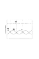
第1のターゲット−基板位置における堆積は膜プロファイル1011を与え、第2の位置における堆積は膜プロファイル1012を与える。このような膜プロファイルは、ゼロ位置からのターゲット−基板位置の比較的に小さな変位における比較的に高いスパッタリング電圧の結果であることがある。比較的に小さな変位は、基板の中央の垂直な平面に関してターゲットアレイが対称である位置、および/または平面ターゲットの場合には平面ターゲットが基板に平行に配置された位置をさす。用語「高い」および「小さい」は、前述の第3および第4の堆積ステップとの比較で使用される。第3の位置における堆積は膜プロファイル1013を与え、第4の位置における堆積は膜プロファイル1014を与える。膜プロファイル1013および1014は、(第1および第2の位置の堆積に比べて)比較的に高い角度での比較的に小さな電圧の結果であることがある。
Deposition at the first target-substrate location provides a
結果として得られる全体の膜プロファイルがプロファイル1020として示されている。このプロファイルは、膜プロファイル1011、1012、1013および1014を有する4つの堆積の重ね合わせである。この略図から明らかなように、結果として得られるプロファイルは高度な均一性を有する。さらに、大部分の材料の堆積が第1および第2の堆積ステップの間に起こるため、処理時間も許容できる範囲である。それには高い堆積力、すなわち高い電圧が必要であるため、ゼロ相対位置からの変位は、第3および第4の堆積ステップに比べて比較的に小さい。それによって、アークを発生させる効果を低減させ、または排除することができる。しかしながら、図9の例から分かるように、堆積させた層1011と1012の間の位相差は180°よりも小さく、そのため、リプル(ripple)は部分的にしか補償されない。
The resulting overall film profile is shown as
図9に示されているように、その結果生じる実質的に相補的な膜分布によって形成される層の均一性の欠如は、第3および第4の堆積ステップを実行することによって補償することができる。すなわち、第3および第4の堆積ステップの目的は主に、第1および第2の堆積ステップによって生み出された膜プロファイルの波形を補償することにある。第3および第4のプロセスステップにおけるゼロ相対位置からの変位は比較的に大きい。アークの発生を回避するために堆積力すなわち電圧が比較的に小さな値に維持されるため、第3および第4のプロセスステップの全体の材料堆積量は小さい。図9に示した例から分かるように、堆積させた層1013と1014の位相差は180°よりも大きい。したがって、典型的には、結果として生じる正弦波プロファイルの位相と、カソードアレイの周期性および/または第1もしくは第2の堆積の層プロファイルの位相とがずれており、そのため、残ったリプルが補償される。
As shown in FIG. 9, the resulting lack of layer uniformity formed by the substantially complementary film distribution can be compensated by performing the third and fourth deposition steps. it can. That is, the purpose of the third and fourth deposition steps is primarily to compensate for the film profile waveforms produced by the first and second deposition steps. The displacement from the zero relative position in the third and fourth process steps is relatively large. Since the deposition force or voltage is maintained at a relatively small value to avoid arcing, the overall material deposition amount of the third and fourth process steps is small. As can be seen from the example shown in FIG. 9, the phase difference between the deposited
記載したステップの順序に代わる適当な任意の順序が可能である。具体的には、ターゲット−基板相対位置を変化させるのに必要な時間を短縮するため、最初に第1および第3のステップを実行し、次に第2および第4のステップを実行することが可能である。これらの4つの堆積ステップの具体的な順序は一般に、処理のサイクル時間および膜の形態学的特性によって決定される。 Any suitable sequence can be substituted for the sequence of steps described. Specifically, in order to reduce the time required to change the target-substrate relative position, the first and third steps may be performed first, and then the second and fourth steps may be performed. Is possible. The specific order of these four deposition steps is generally determined by the processing cycle time and the morphological characteristics of the film.
図11は、回転ターゲット要素120a’から120f’を含む回転ターゲットアレイと基板110との間の相対位置の変化が、基板ワブル方向106に沿った基板110の平行移動(具体的には基板110のワブリング)によって達成される、例示的なコーティングシステム600を示す。この例示的な実施形態では、ターゲット要素120a’から120f’が円筒形の回転ターゲットである。
FIG. 11 shows that the relative position change between the rotating target array including the
したがって、図に示された実施形態に限定されることなく、ターゲット要素(またはターゲット要素のアレイ)に対する基板の移動方向は一般に、基板とターゲット要素の間の距離が一定であり続けるような方向とすることができる。この文脈における句「基板とターゲットの間の距離が一定である」は、基板の表面の全ての点が、1つまたは複数のターゲットの平面から一定の距離のところにあり続けることを意味すると理解すべきである。すなわち、典型的には、ターゲット要素と基板の間の相対位置を基板の表面に平行な方向に変化させる。 Thus, without being limited to the illustrated embodiment, the direction of movement of the substrate relative to the target element (or array of target elements) is generally such that the distance between the substrate and the target element remains constant. can do. The phrase “the distance between the substrate and the target is constant” in this context is understood to mean that all points on the surface of the substrate remain at a certain distance from the plane of the target or targets. Should. That is, typically the relative position between the target element and the substrate is changed in a direction parallel to the surface of the substrate.
より具体的には、図3、6および11に示した実施形態に特に例示されているように、基板と1つまたは複数のターゲットの間の相対的な移動は、回転ターゲットの回転軸に垂直な方向に実施することができ、いくつかの実施形態によれば、基板と1つまたは複数のターゲットの距離が一定になるように実施することができる。この方向を「X方向」と呼ぶこともできる。 More specifically, as specifically illustrated in the embodiments shown in FIGS. 3, 6 and 11, the relative movement between the substrate and one or more targets is perpendicular to the axis of rotation of the rotating target. In some directions, and according to some embodiments, the distance between the substrate and the target or targets can be constant. This direction can also be referred to as the “X direction”.
本明細書に記載された他の実施形態と組み合わせることができる他の実施形態によれば、基板とターゲットのうちの一方を回転させる。例えば、この回転は、往復するように実施することができ、それによって、基板は、基板と1つまたは複数のターゲット要素の間の相対位置を変化させる。図12は、基板を回転させるように適合されたコーティングシステムの例示的な一実施形態を示す。例示のため、図12には角度βが示されている。この例示的な実施形態では、この角度の絶対値が、基板の両方の外側位置IおよびIIで同じである。あるいは、一方の外側位置ともう一方の外側位置とでこの角度の絶対値が異なっていてもよい。典型的な実施形態によれば、この角度の絶対値が50度未満、より具体的には45度未満、さらに具体的には30度未満である。いくつかの実施形態では、外側位置(IおよびII)に基板を保持し、他の実施形態によれば、基板を絶え間なく移動させる。 According to other embodiments that can be combined with other embodiments described herein, one of the substrate and the target is rotated. For example, this rotation can be performed to reciprocate, whereby the substrate changes the relative position between the substrate and one or more target elements. FIG. 12 illustrates an exemplary embodiment of a coating system adapted to rotate a substrate. For illustration, the angle β is shown in FIG. In this exemplary embodiment, the absolute value of this angle is the same at both outer positions I and II of the substrate. Alternatively, the absolute value of this angle may be different between one outer position and the other outer position. According to a typical embodiment, the absolute value of this angle is less than 50 degrees, more specifically less than 45 degrees, and more specifically less than 30 degrees. In some embodiments, the substrate is held in outer positions (I and II), and according to other embodiments, the substrate is moved continuously.
これまでに示した相対位置の変化は、ターゲット要素および/または基板を典型的には基板表面に平行な方向に移動させるものであった。以下で説明する図に示すように、少なくとも1つのターゲットと基板の間の距離が変化するように、少なくとも1つのターゲットと基板の間の相対位置を変化させることも可能である。言い換えると、基板および1つまたは複数のターゲットが、互いに近づく方向へ移動するように、および/または互いから遠ざかる方向へ移動するように、相対位置を変化させる。例えば、最初にターゲットと基板の間の距離を縮め、その後に、例えばある位置で静止した後で、この距離を再び広げることができる。 The relative position changes shown so far have moved the target element and / or the substrate, typically in a direction parallel to the substrate surface. As shown in the figures described below, the relative position between the at least one target and the substrate can be varied such that the distance between the at least one target and the substrate varies. In other words, the relative position is changed so that the substrate and the one or more targets move in a direction toward each other and / or move away from each other. For example, the distance between the target and the substrate can first be reduced, and then the distance can be increased again after, for example, resting at a certain position.
図13は、円筒形のターゲット310の前に基板110が配置された実施形態を示し、図14は、平面ターゲット530の前に基板110が配置された実施形態を示す。基板およびターゲットの向きは水平または垂直とすることができる。例示の目的上、図13および14にはターゲットが1つしか示されていないが、多数のターゲットを配置することも可能である。矢印106によって示されているように、基板キャリア104の位置を変化させることによって、基板110と平面カソードアセンブリ502の相対位置を変化させる。例えば、基板の向きが水平である場合には、基板を上げ下げすることができる。基板の向きが垂直である場合には、(ターゲットの方向に)基板を前後に移動させることができる。いずれにせよ、基板とターゲットの間の全体距離を変化させ、基板上のコーティングの分布を変化させて、前述のとおりにコーティングの結果を向上させる。
FIG. 13 illustrates an embodiment in which the
句「ターゲットと基板の間の全体距離を変化させる」は、基板が、全体として、ターゲットへ近づく方向へ移動し、および/またはターゲットから遠ざかる方向へ移動することを意味すると理解すべきである。あるいはまたはそれに加えて、ターゲットが、全体として、基板へ近づく方向へ移動し、および/または基板から遠ざかる方向へ移動する。対照的に、用語「回転する」は、ターゲットおよび基板の表面の一部の点が互いに接近し、それと同時に、ターゲットおよび基板の別の点が互いから遠ざかることを意味する。1つもしくは複数のターゲットまたは基板を「回転させる」ことは通常、少なくとも回転軸(通常はターゲットもしくは基板の内部またはターゲットもしくは基板上にある)が、前記1つもしくは複数のターゲットまたは基板から一定の距離のところにあり続けることを含む。 The phrase “changing the overall distance between the target and the substrate” should be understood to mean that the substrate as a whole moves in a direction towards and / or away from the target. Alternatively or in addition, the target moves generally toward the substrate and / or away from the substrate. In contrast, the term “rotate” means that some points on the surface of the target and the substrate are close to each other while other points on the target and the substrate are away from each other. “Rotating” one or more targets or substrates typically has at least a rotational axis (usually within or on the target or substrate) that is constant from the one or more targets or substrates. Including staying at a distance.
一般に、ターゲットのアレイの場合には、基板とターゲットの間の距離が一定でないような相対位置の変化も可能である。典型的には、基板とターゲットの間の相対的な移動の方向が、基板表面からの垂線に沿った方向である。本明細書ではこの方向を「Z方向」と呼ぶ。例えば、図15は、回転ターゲット120a’から120f’のアレイを示し、この例では、基板を、これらの回転ターゲットに対して上下に(基板の向きが垂直の場合には前後に)、例えば往復するように移動させる。図示されてはいないが、回転ターゲットのアレイの代わりに平面カソードアセンブリのアレイを同様に配置することも可能である。
In general, in the case of an array of targets, the relative position can be changed such that the distance between the substrate and the target is not constant. Typically, the direction of relative movement between the substrate and the target is a direction along a normal from the substrate surface. In this specification, this direction is referred to as a “Z direction”. For example, FIG. 15 shows an array of
いくつかの実施形態によれば、基板を移動させる代わりに、または基板を移動させることに加えて、1つのターゲットまたはターゲット要素のアレイを移動させることも可能である。 According to some embodiments, instead of moving the substrate or in addition to moving the substrate, it is also possible to move one target or an array of target elements.
本開示は、基板の位置を、少なくとも1つのターゲットに対して相対的に変化させることを対象としている。基板および/またはターゲットの1次元移動を提供することが可能だが、図5、7および11に関して示したように回転運動を提供することも可能である。したがって、これらの実施形態では、通常は基板または少なくとも1つのターゲットの重心の軸である軸を軸に、ターゲットおよび/または基板を回転させる。 The present disclosure is directed to changing the position of the substrate relative to at least one target. While it is possible to provide a one-dimensional movement of the substrate and / or target, it is also possible to provide a rotational movement as shown with respect to FIGS. Thus, in these embodiments, the target and / or substrate is rotated about an axis that is typically the axis of gravity of the substrate or at least one target.
図16および17は、基板とターゲットの間の相対的な円運動を示す。図16および17ではこの相対的な円運動が、単一の回転カソードアセンブリに関して示されているが、回転カソードアセンブリのアレイの場合にもまたは1つもしくは複数の平面カソードの場合にも、同じ相対運動を提供することができることを理解すべきである。 16 and 17 show the relative circular motion between the substrate and the target. Although this relative circular motion is shown in FIGS. 16 and 17 for a single rotating cathode assembly, it is the same relative for an array of rotating cathode assemblies or for one or more planar cathodes. It should be understood that exercise can be provided.
図16および17に示した実施形態によれば、基板を、円を描くように移動させる。この文脈における用語「円」はさらに、完全な楕円形または部分的な楕円形の移動経路を含む。一般に、この文脈における「円」は特に、基板および/またはターゲットの移動が2次元以上、例えば2次元の移動であることを示す。図16および17にはほぼ完全な円が示されているが、この運動は、例えば最大90°または60°の扇形など、円または楕円の一部だけをカバーするものであってもよい。 According to the embodiment shown in FIGS. 16 and 17, the substrate is moved in a circle. The term “circle” in this context further includes a full or partial elliptical travel path. In general, a “circle” in this context specifically indicates that the movement of the substrate and / or target is two or more dimensions, for example, a two-dimensional movement. Although a nearly perfect circle is shown in FIGS. 16 and 17, this movement may cover only a portion of the circle or ellipse, for example a sector of up to 90 ° or 60 °.
図18および19は、1つまたは複数のターゲット要素と基板の間の相対位置を、1つまたは複数のターゲット要素に平行な方向へ変化させる本開示の実施形態を示す。示されているように、ターゲット要素は回転ターゲットとすることができ、回転ターゲットの回転軸が、相対位置を変化させる方向を画定する。回転ターゲットの回転軸によって画定される方向を「Y方向」と呼ぶ。図18に示すように、1つまたは複数のターゲットをY方向へ移動させることができる。図19に示すように、基板をY方向へ移動させることもできる。基板と1つまたは複数のターゲットの両方を例えばY方向へ移動させることも可能である。 18 and 19 illustrate embodiments of the present disclosure that change the relative position between one or more target elements and the substrate in a direction parallel to the one or more target elements. As shown, the target element can be a rotating target, and the axis of rotation of the rotating target defines the direction in which the relative position changes. A direction defined by the rotation axis of the rotation target is referred to as a “Y direction”. As shown in FIG. 18, one or more targets can be moved in the Y direction. As shown in FIG. 19, the substrate can also be moved in the Y direction. It is also possible to move both the substrate and one or more targets, for example in the Y direction.
Y方向へ相対的に移動させた場合には、スパッタされた材料の分布が全く変化しないと予想することもできるが、実験によれば、相対位置をY方向に沿って変化させることによっても全体的な層の均一性を向上させることができる。 Although it can be expected that the distribution of the sputtered material does not change at all when moved relative to the Y direction, according to experiments, the entire position can also be changed by changing the relative position along the Y direction. Layer uniformity can be improved.
この実施形態に限定されることなく、本明細書に記載された実施形態は一般に、X方向、Y方向もしくはY方向の1次元移動またはこれらの方向を重ね合わせた方向の1次元移動を含む。他の実施形態は、2次元以上の移動、例えば基板の表面に平行な2次元平面(例えばXY平面)内の移動、基板の表面と(例えば90°の角度で)交差する2次元平面(例えばXZ平面またはYZ平面)内の移動、または3次元移動(したがって3つの方向X、YおよびZを全て含む)を提供する。 Without being limited to this embodiment, the embodiments described herein generally include a one-dimensional movement in the X, Y, or Y direction or a one-dimensional movement in the direction of superimposing these directions. Other embodiments provide two or more dimensions of movement, eg, movement in a two-dimensional plane (eg, XY plane) parallel to the surface of the substrate, two-dimensional plane (eg, at a 90 ° angle) intersecting the surface of the substrate (eg Provide movement in the XZ plane or YZ plane), or three-dimensional movement (thus including all three directions X, Y and Z).
本明細書に記載された実施形態はさらに、基板の処理中、例えば基板表面に材料を堆積させている間、マスクおよび基板を保持するように適合された保持装置を提供し、またはそのような保持装置を利用することができる。処理中に基板を移動させる場合には、保持装置も移動させる。スパッタリング中、保持装置は通常、基板に常に接続されている。具体的には、保持装置は、基板を担持するように適合された基板キャリア、および基板をマスキングするためのマスクを含むことができ、マスクは、基板キャリアに取り外し可能に接続される。基板キャリアまたはマスクは通常、堆積の間、基板キャリアを覆うカバーを受け取るように適合された少なくとも1つの凹みを有する。 The embodiments described herein further provide a holding device adapted to hold the mask and the substrate during processing of the substrate, eg, while depositing material on the substrate surface, or such A holding device can be used. When the substrate is moved during processing, the holding device is also moved. During sputtering, the holding device is usually always connected to the substrate. Specifically, the holding device can include a substrate carrier adapted to carry a substrate and a mask for masking the substrate, the mask being removably connected to the substrate carrier. The substrate carrier or mask typically has at least one recess adapted to receive a cover covering the substrate carrier during deposition.
典型的な実施形態によれば、マスクは、基板上の、通常は基板の縁に沿ったあるエリアをコーティングされていない状態に保つために使用される。いくつかの静止アレイ用途ではこれが必要になることがある。 According to an exemplary embodiment, the mask is used to keep an area on the substrate, usually along the edge of the substrate, uncoated. This may be necessary for some stationary array applications.
マスキング、特に基板の縁のマスキングの追加の詳細については、(2010年9月17日にApplied Materials,Inc.の名義で出願された)欧州特許出願第10177419号および(2010年9月24日にApplied Materials,Inc.の名義で出願された)米国特許出願第12/890,194号、特に、これらの文献の基板の縁のマスキングについて述べている部分を参照されたい。これらの文献は、参照により、本開示と矛盾しない範囲で本明細書に組み込まれる。 For additional details of masking, particularly masking of the edges of the substrate, see European Patent Application No. 10177419 (filed in the name of Applied Materials, Inc. on September 17, 2010) and (on September 24, 2010). See US patent application Ser. No. 12 / 890,194 (filed in the name of Applied Materials, Inc.), and in particular, the portion of these documents describing the masking of the edges of a substrate. These documents are incorporated herein by reference to the extent they do not conflict with the present disclosure.
本開示の実施形態は、基板をコーティングする方法をさらに含み、この方法は、スパッタされた材料の層を基板上に形成することを含み、スパッタされた材料の層を形成することは、少なくとも2つの異なる膜分布を重ね合わせることを含む。これらの膜分布はそれぞれ、上記の任意の実施形態に従って、すなわち、ターゲット−基板相対位置を変化させ、所定の時間間隔の間、スパッタリングを実行することによって形成することができる。あるいは、これらの膜分布は、2010年9月30日にApplied Materialsによって欧州特許庁に出願されたPCT出願「Method For Coating A Substrate And Coater」、特に、この文献の異なる磁石アセンブリ位置における異なる材料分布の形成について述べている部分に記載されている磁石ワブリングによって形成することもできる。この文献は、参照により、本開示と矛盾しない範囲で本明細書に組み込まれる。 Embodiments of the present disclosure further include a method of coating a substrate, the method including forming a layer of sputtered material on the substrate, and forming the layer of sputtered material is at least 2 Including superimposing two different membrane distributions. Each of these film distributions can be formed according to any of the above embodiments, i.e., by changing the target-substrate relative position and performing sputtering for a predetermined time interval. Alternatively, these film distributions can be found in PCT application “Method For Coating A Substrate And Coater” filed by Applied Materials on September 30, 2010, in particular, different material distributions at different magnet assembly positions in this document. It can also be formed by magnet wobbling as described in the section describing the formation of. This document is incorporated herein by reference to the extent not inconsistent with the present disclosure.
最後の実施形態のうちの少なくともいくつかの実施形態によれば、少なくとも2つの膜分布が実質的に相補的である。さらに、材料のスパッタリングは、前記少なくとも2つの膜分布の形状が実質的に正弦波の形になるように配置された複数のターゲットから実行することができる。 According to at least some of the last embodiments, the at least two membrane distributions are substantially complementary. Furthermore, sputtering of the material can be performed from a plurality of targets arranged such that the shape of the at least two film distributions is substantially sinusoidal.
典型的な実施形態によれば、層形成中に、厚さの均一性が少なくとも±10%、好ましくは少なくとも±5%、さらに好ましくは少なくとも±1%であるスパッタされた材料の層が形成されるように、相対位置を変化させる。 According to a typical embodiment, during layer formation, a layer of sputtered material having a thickness uniformity of at least ± 10%, preferably at least ± 5%, more preferably at least ± 1% is formed. As shown, the relative position is changed.
本明細書に開示された任意の実施形態と組み合わせることができるある種の実施形態によれば、基板の最終的なワブルに加えて、コーティング中に、基板を、(例えば、限定はされないが、基板コンベヤによって)一方向へ連続的に移動させることができる(すなわち「動的コーティング」)。代替実施形態によれば、限定はされないが、コーティングする基板をゼロ位置に配置し、またはゼロ位置を中心にワブリングさせる。このゼロ位置はコーティング中、動かない(「静的コーティング」)。動的コーティング中には基板コンベヤもコーティングされる可能性があるため、静的コーティングは一般に、動的コーティングに比べて高い効率が得やすい。静的コーティングは特に、大面積基板のコーティングを容易にする。典型的な実施形態によれば、静的コーティングによって、基板は、層形成が実行されるコーティングエリアへ入れられ、コーティングが実行され、基板は再びコーティングエリアの外へ運ばれる。 According to certain embodiments that can be combined with any embodiment disclosed herein, in addition to the final wobble of the substrate, during coating, the substrate (e.g., but not limited to) It can be moved continuously in one direction (i.e. "dynamic coating"). According to an alternative embodiment, but not limited to, the substrate to be coated is placed in a zero position or wobbled around the zero position. This zero position does not move during coating (“static coating”). Static coating is generally more efficient than dynamic coating because substrate conveyors can also be coated during dynamic coating. Static coatings in particular facilitate the coating of large area substrates. According to an exemplary embodiment, by static coating, the substrate is placed into the coating area where layering is performed, the coating is performed, and the substrate is again transported out of the coating area.
ある種の実施形態によれば、導電層製造プロセスおよび/またはシステムが提供される。この製造プロセスおよび/またはシステムは、(特にTFTの)電極またはバスを製造するプロセスおよび/またはシステムとすることができる。この製造プロセスおよび/またはシステムはそれぞれ、本明細書の実施形態に従って基板をコーティングする方法および/またはシステムを含む。例えば、限定はされないが、このような導電層は金属層とすることができ、または、限定はされないがITO(酸化インジウムスズ)層などの透明な導電層とすることができる。 According to certain embodiments, a conductive layer manufacturing process and / or system is provided. This manufacturing process and / or system may be a process and / or system for manufacturing an electrode or bus (especially for a TFT). Each of the manufacturing processes and / or systems includes a method and / or system for coating a substrate in accordance with embodiments herein. For example, without limitation, such a conductive layer can be a metal layer, or can be a transparent conductive layer such as, but not limited to, an ITO (indium tin oxide) layer.
本開示の少なくともいくつかの実施形態は特に、大面積基板のコーティングを対象とする。一般に、用語「大面積基板」は、少なくとも1500mm×1800mmのサイズを有する基板を含む。ある種の実施形態によれば、TFT−LCDディスプレイの製造プロセスおよび/または製造システムが提供される。このTFT−LCDディスプレイ製造プロセスおよび/またはシステムはそれぞれ、本明細書の実施形態に従って基板をコーティングする方法および/またはシステムを含む。 At least some embodiments of the present disclosure are particularly directed to coating large area substrates. In general, the term “large area substrate” includes a substrate having a size of at least 1500 mm × 1800 mm. According to certain embodiments, a TFT-LCD display manufacturing process and / or manufacturing system is provided. Each of the TFT-LCD display manufacturing processes and / or systems includes a method and / or system for coating a substrate in accordance with embodiments herein.
他の実施形態によれば、薄膜太陽電池の製造プロセスおよび/または製造システムが提供される。この薄膜太陽電池製造プロセスおよび/またはシステムはそれぞれ、本明細書の実施形態に従って基板をコーティングする方法および/またはシステムを含む。特定の実施形態によれば、この薄膜太陽電池製造プロセスが、TCO層および/またはバックコンタクト層のスパッタリングを含む。任意選択で、この薄膜太陽電池製造プロセスは、化学気相堆積による吸収層の堆積を含む。 According to another embodiment, a thin film solar cell manufacturing process and / or system is provided. Each of the thin film solar cell manufacturing processes and / or systems includes a method and / or system for coating a substrate in accordance with embodiments herein. According to certain embodiments, the thin film solar cell manufacturing process includes sputtering of the TCO layer and / or the back contact layer. Optionally, the thin film solar cell manufacturing process includes the deposition of an absorber layer by chemical vapor deposition.
例えば、本開示の少なくともいくつかの実施形態は、ガラス基板上に形成されたアルミニウム層の抵抗率に関して高い均一性を提供することができる。例えば、面積抵抗Rsに関して、406mm×355mmの基板エリア全体にわたって±1%から±4%の間または±0.5%から±3%の間の均一性を達成することができる。 For example, at least some embodiments of the present disclosure can provide high uniformity with respect to the resistivity of an aluminum layer formed on a glass substrate. For example, a uniformity between ± 1% and ± 4% or between ± 0.5% and ± 3% can be achieved over the entire substrate area of 406 mm × 355 mm with respect to the sheet resistance Rs.
ある種の実施形態によれば、大面積基板をコーティングするために、円筒形の回転ターゲット、平面ターゲットなどのターゲットをそれぞれが含む複数のカソードアセンブリが提供される。基板をコーティングするように適合された室を「コーティング室」と呼ぶ。1度に1枚の基板をコーティングするようにそれぞれが適合された複数のコーティング室を提供することができる。多数の基板を次々にコーティングすることができる。 According to certain embodiments, a plurality of cathode assemblies are provided that each include a target, such as a cylindrical rotating target, a planar target, etc., for coating a large area substrate. A chamber adapted to coat a substrate is referred to as a “coating chamber”. Multiple coating chambers can be provided, each adapted to coat one substrate at a time. Multiple substrates can be coated one after the other.
以上に、コーティングシステム用のシステムおよび方法の例示的な実施形態を詳細に説明した。それらのシステムおよび方法は、本明細書に記載された特定の実施形態に限定されない。それらのシステムの構成要素および/またはそれらの方法のステップは、本明細書に記載された他の構成要素および/またはステップから独立して別々に利用することができる。 The foregoing has described in detail exemplary embodiments of systems and methods for coating systems. Those systems and methods are not limited to the specific embodiments described herein. Those system components and / or method steps may be utilized separately and independently of other components and / or steps described herein.
図に示した実施形態は、水平に配置された基板の上方に配置されたターゲットを例示しているが、空間内の基板の向きを垂直にすることもできることを付言しておく。特に、大面積コーティングを考えると、基板の向きを垂直にした場合には、基板の輸送および取扱いが単純になり、容易になると思われる。他の実施形態では、水平の向きと垂直の向きの間のいずれかの向きに基板を配置することも可能である。 The embodiment shown in the figure illustrates the target disposed above the horizontally disposed substrate, but it should be noted that the orientation of the substrate in the space may be vertical. Considering large area coatings in particular, it is likely that transport and handling of the substrate will be simplified and facilitated when the substrate orientation is vertical. In other embodiments, the substrate can be placed in any orientation between a horizontal orientation and a vertical orientation.
本開示の範囲内では、少なくともいくつかの図が、コーティングシステムおよび基板の概略断面図を示す。示されたターゲットのうちの少なくともいくつかのターゲットは円筒として形成される。それらの図面では、図面を見たときに、ターゲットが紙面の奥へおよび紙面から外へ延びていることに留意すべきである。同じく断面図の要素として概略的に示されているだけである磁石アセンブリについても同じことが言える。磁石アセンブリは、円筒形のターゲットによって画定される円筒の全長に沿って延びることができる。技術的な理由から、磁石アセンブリは、典型的には円筒の全長の少なくとも80%、より典型的には円筒の全長の少なくとも90%にわたって延びる。 Within the scope of this disclosure, at least some of the figures show schematic cross-sectional views of the coating system and the substrate. At least some of the targets shown are formed as cylinders. In these drawings, it should be noted that the target extends to the back of the page and out of the page when viewed. The same is true for a magnet assembly which is also only schematically shown as a cross-sectional element. The magnet assembly can extend along the entire length of the cylinder defined by the cylindrical target. For technical reasons, the magnet assembly typically extends at least 80% of the total length of the cylinder, more typically at least 90% of the total length of the cylinder.
本明細書で使用されるとき、「1つの(a)」、「1つの(an)」、「少なくとも1つの(at least one)」および「1つまたは複数の(one or more)」は相互に交換可能に使用される。本明細書ではさらに、終点による数値範囲の説明が、その範囲内に包含される全ての数値を含む(例えば、1から5は、1、1.5、2、2.75、3、3.80、4、5、などを含む)。 As used herein, “an”, “an”, “at least one” and “one or more” are mutually exclusive. Used interchangeably. Further herein, the recitations of numerical ranges by endpoints include all numbers subsumed within that range (eg 1 to 5 is 1, 1.5, 2, 2.75, 3, 3,. 80, 4, 5, etc.).
本発明のさまざまな実施形態の特定の特徴が一部の図面には示されており、他の図面には示されていないことがあるが、これは単に便宜上のことである。本発明の原理に従って、図面の任意の特徴を参照し、かつ/または他の図面の任意の特徴と組み合わせて請求することができる。 Although specific features of various embodiments of the invention may be shown in some drawings and not in others, this is for convenience only. In accordance with the principles of the invention, any feature of a drawing may be referenced and / or combined with any feature of any other drawing.
本明細書は、本発明を、その最良の形態を含めて開示するため、さらには当業者が本発明を実施することを可能にするために、いくつかの例を使用する。本発明を実施することには、装置またはシステムを製作し使用すること、および組み込まれた方法を実行することが含まれる。以上に、さまざまな特定の実施形態を開示したが、特許請求の趣旨および範囲が、等しく有効な変更を見込んでいることを当業者は理解するであろう。特に、上述の実施形態の相互に排除しない特徴は互いに組み合わせることができる。本発明の特許を受けられる範囲は、特許請求の範囲によって定義され、特許を受けられる範囲が、当業者が思いつく他の例を含むことがある。このような他の例は、それらが特許請求の範囲の文字表現と異ならない構造要素を有する場合、またはそれらが特許請求の範囲の文字表現との差異が実質的にない等価の構造要素を含む場合に、特許請求の範囲に含まれることが意図されている。
また、本願は以下に記載する態様を含む。
(態様1)
基板(110)をコーティングする方法であって、前記方法は、
スパッタされた材料の層(806)を前記基板(110)上に形成することを含み、スパッタされた材料の前記層を形成することが、
少なくとも1つの回転ターゲット(120’)から材料を前記基板(110)の上方にスパッタすること、および
前記少なくとも1つの回転ターゲット(120’)と前記基板(110)の間の相対位置を変化させること
を含む方法。
(態様2)
変化させることが、
前記少なくとも1つの回転ターゲット(120’)と前記基板(110)の間の相対位置を第1の位置(I)へ変化させ、前記第1の位置を、所定の第1の時間間隔の間、維持すること、および
前記少なくとも1つの回転ターゲットと前記基板の間の相対位置を第2の位置(II)へ変化させ、前記第2の位置を、所定の第2の時間間隔の間、維持すること
を含み、
前記所定の第1の時間間隔と前記所定の第2の時間間隔のうちの少なくとも一方が、任意選択で少なくとも0.1秒、好ましくは少なくとも0.5秒、さらに好ましくは少なくとも1秒である、
態様1に記載の基板をコーティングする方法。
(態様3)
前記少なくとも1つの回転ターゲット(120’)が回転ターゲットのアレイである、態様1または2に記載のコーティング方法。
(態様4)
前記回転ターゲット(120’、120”)に関連づけられたカソードアセンブリ(310、502)に電圧を印加すること
をさらに含み、
前記相対位置を変化させることが、前記相対位置を前記第1の位置から前記第2の位置へ変化させることを含み、前記相対位置が前記第1または第2の位置に対応するときの方が、前記相対位置が前記第1の位置と前記第2の位置の間の位置に対応するときよりも、前記電圧が高い、
態様1ないし3のいずれか一項に記載のコーティング方法。
(態様5)
前記相対位置が前記第1の位置と前記第2の位置の間の位置に対応するときに前記電圧が実質的にゼロであり、及び/または、前記相対位置を変化させている間に、前記電圧を、時間の経過とともに、方形波の波形に従って変化させる、態様4に記載のコーティング方法。
(態様6)
厚さの均一性が少なくとも±10%、好ましくは少なくとも±5%、さらに好ましくは少なくとも±1%であるスパッタされた材料の前記層が形成されるような態様で、前記相対位置を変化させる、態様1ないし5のいずれか一項に記載のコーティング方法。
(態様7)
前記相対位置を変化させることが、スパッタされた材料の前記層を形成する前記基板の表面に実質的に平行な平面に沿って、前記基板(110)を、前記少なくとも1つの回転ターゲット(120)に対して変位させることを含む、態様1ないし6のいずれか一項に記載のコーティング方法。
(態様8)
前記回転ターゲットが、その円筒対称軸を軸に回転可能な実質的に円筒形のターゲット(120’)である、態様1ないし7のいずれか一項に記載のコーティング方法。
(態様9)
基板(110)をコーティングする方法であって、
スパッタされた材料の層を前記基板(110)上に形成することを含み、スパッタされた材料の前記層を形成することが、
少なくとも1つのターゲット(120、120’、120”)から材料を前記基板の上方にスパッタすること、および
前記少なくとも1つのターゲットと前記基板(110)の間の相対位置を、前記少なくとも1つのターゲットと前記基板の間の距離を変化させることによって変化させること
を含む方法。
(態様10)
前記少なくとも1つのターゲット(120)から材料をスパッタすることが、少なくとも2つの膜分布(802、804)を重ね合わせることを含み、任意選択で、前記少なくとも2つの膜分布(802、804)が実質的に相補的である、態様1ないし9のいずれか一項に記載の方法。
(態様11)
材料をスパッタすることが、前記少なくとも2つの膜分布の形状が実質的に正弦波の形になるように配置された回転ターゲットまたは好ましくは回転可能な複数のターゲット(120a’、120b’、120c’、120d’、120e’、120f’、120a”、120b”、120c”、120d”)から実行される、態様9または10に記載の方法。
(態様12)
基板をコーティングするシステムであって、材料を前記基板(110)上でスパッタするための少なくとも1つの回転ターゲット(120’)を備え、前記少なくとも1つの回転ターゲット(120’)が、前記基板(110)のコーティング中に、前記少なくとも1つの回転ターゲット(120’)と前記基板(110)の間の相対位置が変化するような態様で移動するよう構成されたシステム。
(態様13)
前記少なくとも1つの回転ターゲット(120’)が、回転ターゲット(120a’、120b’、120c’、120d’、120e’、120f’)のアレイである、態様12に記載の基板をコーティングするシステム。
(態様14)
基板をコーティングするシステムであって、材料を前記基板(110)上でスパッタするための少なくとも1つのターゲット(120、120’、120”)を備え、前記少なくとも1つのターゲットが、前記基板(110)のコーティング中に、前記少なくとも1つのターゲット(120、120’、120”)と前記基板(110)の間の距離が変化するような態様で移動するように構成されたシステム。
(態様15)
前記少なくとも1つのターゲットが、回転ターゲット(120)または回転ターゲット(120a’、120b’、120c’、120d’、120e’、120f’)のアレイである、態様14に記載の基板をコーティングするシステム。
(態様16)
基板(110)をコーティングする方法であって、前記方法は、
スパッタされた材料の層を前記基板(110)上に形成することを含み、スパッタされた材料の前記層を形成することが、
少なくとも1つの実質的に円筒形のターゲット(120’)である回転ターゲット(120’)をその円筒対象軸に回転させ、かつ、少なくとも1つの回転ターゲット(120’)から材料を前記基板の上方にスパッタすること、および
前記少なくとも1つの回転ターゲットと前記基板(110)の間の相対位置を、前記少なくとも1つの回転ターゲットと前記基板の間の距離を変化させることによって変化させること
を含む方法。
(態様17)
基板をコーティングするシステムであって、材料を前記基板(110)上でスパッタするための少なくとも1つの回転ターゲット(120、120’、120”)を備え、前記少なくとも1つのターゲットが、前記基板(110)のコーティング中に、前記少なくとも1つのターゲット(120、120’、120”)と前記基板(110)の間の距離が変化するような態様で移動するように構成され、
前記回転ターゲットが実質的に円筒形のターゲット(120’)であり、その円筒対象軸に回転可能である、システム。
This written description uses examples to disclose the invention, including its best mode, and also to enable any person skilled in the art to practice the invention. Implementing the present invention includes making and using the apparatus or system and performing the incorporated methods. While various specific embodiments have been disclosed above, those skilled in the art will appreciate that the spirit and scope of the claims contemplates equally effective modifications. In particular, the features of the embodiments described above that are not excluded from one another can be combined with one another. The patentable scope of the invention is defined by the claims, and the patentable scope may include other examples that occur to those skilled in the art. Such other examples include equivalent structural elements where they have structural elements that do not differ from the character representation of the claims, or where they do not substantially differ from the character representation of the claims. In some cases, it is intended to be within the scope of the claims.
Moreover, this application contains the aspect described below.
(Aspect 1)
A method of coating a substrate (110), the method comprising:
Forming a layer of sputtered material (806) on the substrate (110), and forming the layer of sputtered material;
Sputtering material from at least one rotating target (120 ′) onto the substrate (110); and
Changing the relative position between the at least one rotating target (120 ′) and the substrate (110);
Including methods.
(Aspect 2)
To change
The relative position between the at least one rotating target (120 ′) and the substrate (110) is changed to a first position (I), and the first position is changed during a predetermined first time interval. Maintaining, and
Changing the relative position between the at least one rotating target and the substrate to a second position (II), and maintaining the second position for a predetermined second time interval;
Including
At least one of the predetermined first time interval and the predetermined second time interval is optionally at least 0.1 seconds, preferably at least 0.5 seconds, more preferably at least 1 second;
A method for coating a substrate according to aspect 1.
(Aspect 3)
A coating method according to aspect 1 or 2, wherein the at least one rotating target (120 ') is an array of rotating targets.
(Aspect 4)
Applying a voltage to the cathode assembly (310, 502) associated with the rotating target (120 ', 120 ")
Further including
Changing the relative position includes changing the relative position from the first position to the second position, and when the relative position corresponds to the first or second position. The voltage is higher than when the relative position corresponds to a position between the first position and the second position;
The coating method according to any one of aspects 1 to 3.
(Aspect 5)
While the voltage is substantially zero when the relative position corresponds to a position between the first position and the second position, and / or while changing the relative position, the 5. The coating method according to aspect 4, wherein the voltage is changed according to a square wave waveform with time.
(Aspect 6)
Changing the relative position in such a way that the layer of sputtered material having a thickness uniformity of at least ± 10%, preferably at least ± 5%, more preferably at least ± 1% is formed; The coating method according to any one of aspects 1 to 5.
(Aspect 7)
Changing the relative position causes the substrate (110) to move the at least one rotating target (120) along a plane substantially parallel to the surface of the substrate forming the layer of sputtered material. The coating method as described in any one of aspect 1 thru | or 6 including displacing with respect to.
(Aspect 8)
The coating method according to any one of aspects 1 to 7, wherein the rotating target is a substantially cylindrical target (120 ') rotatable about its cylindrical symmetry axis.
(Aspect 9)
A method of coating a substrate (110) comprising:
Forming a layer of sputtered material on the substrate (110), and forming the layer of sputtered material;
Sputtering material onto the substrate from at least one target (120, 120 ′, 120 ″);
Changing the relative position between the at least one target and the substrate (110) by changing the distance between the at least one target and the substrate;
Including methods.
(Aspect 10)
Sputtering material from the at least one target (120) includes overlaying at least two film distributions (802, 804), and optionally the at least two film distributions (802, 804) are substantially 10. A method according to any one of aspects 1 to 9, which is complementary in nature.
(Aspect 11)
Sputtering material is a rotating target or preferably a plurality of rotatable targets (120a ′, 120b ′, 120c ′) arranged such that the shape of the at least two film distributions is substantially sinusoidal. 120d ′, 120e ′, 120f ′, 120a ″, 120b ″, 120c ″, 120d ″).
(Aspect 12)
A system for coating a substrate comprising at least one rotating target (120 ') for sputtering material onto the substrate (110), wherein the at least one rotating target (120') is the substrate (110). ) In such a manner that the relative position between the at least one rotating target (120 ′) and the substrate (110) changes.
(Aspect 13)
A system for coating a substrate according to aspect 12, wherein the at least one rotating target (120 ′) is an array of rotating targets (120a ′, 120b ′, 120c ′, 120d ′, 120e ′, 120f ′).
(Aspect 14)
A system for coating a substrate comprising at least one target (120, 120 ′, 120 ″) for sputtering material onto the substrate (110), wherein the at least one target is the substrate (110). A system configured to move in such a manner that the distance between the at least one target (120, 120 ′, 120 ″) and the substrate (110) varies during coating.
(Aspect 15)
15. The system for coating a substrate according to aspect 14, wherein the at least one target is a rotating target (120) or an array of rotating targets (120a ′, 120b ′, 120c ′, 120d ′, 120e ′, 120f ′).
(Aspect 16)
A method of coating a substrate (110), the method comprising:
Forming a layer of sputtered material on the substrate (110), and forming the layer of sputtered material;
At least one substantially cylindrical target (120 ′), which is a rotating target (120 ′), is rotated about its cylindrical object axis, and material from at least one rotating target (120 ′) is over the substrate. Sputtering, and changing a relative position between the at least one rotating target and the substrate (110) by changing a distance between the at least one rotating target and the substrate.
(Aspect 17)
A system for coating a substrate comprising at least one rotating target (120, 120 ′, 120 ″) for sputtering material onto the substrate (110), wherein the at least one target is the substrate (110). ) In a manner such that the distance between the at least one target (120, 120 ′, 120 ″) and the substrate (110) varies ,
The system wherein the rotating target is a substantially cylindrical target (120 ') and is rotatable about its cylindrical object axis .
Claims (13)
外側回転ターゲットと該外側回転ターゲットの間にある内側回転ターゲットとを有した回転ターゲットのアレイで、スパッタされた材料の層(806)を前記基板(110)上に形成することを含み、スパッタされた材料の前記層を形成することが、
前記回転ターゲットのアレイのうち少なくとも一つの回転ターゲット(120’)であって、実質的に円筒形のターゲット(120’)である少なくとも一つの回転ターゲット(120’)をその円筒対象軸を軸に回転させ、かつ、前記少なくとも1つの回転ターゲット(120’)から材料を前記基板(110)の上方にスパッタすることとであって、前記外側回転ターゲットが前記内側回転ターゲットより前記基板に近いか、または前記内側回転ターゲットが前記外側回転ターゲットより前記基板に近いことと、
前記少なくとも1つの回転ターゲット(120’)と前記基板(110)の間の相対位置を第1の位置(I)へ変化させ、前記第1の位置を所定の第1の時間間隔の間、維持することと、
前記少なくとも1つの回転ターゲットと前記基板の間の前記相対位置を第2の位置(II)へ変化させ、前記第2の位置を、所定の第2の時間間隔の間、維持することと
を含み、前記所定の第1の時間間隔と前記所定の第2の時間間隔のうちの少なくとも一方が少なくとも1秒である方法。 A method of coating a substrate (110), the method comprising:
An array of rotating targets having an outer rotating target and an inner rotating target between the outer rotating targets , comprising forming a layer of sputtered material (806) on the substrate (110) and being sputtered. Forming said layer of material,
At least one rotating target (120 ′) of the rotating target array, wherein at least one rotating target (120 ′) is a substantially cylindrical target (120 ′). Rotating and sputtering material from the at least one rotating target (120 ′) onto the substrate (110) , wherein the outer rotating target is closer to the substrate than the inner rotating target; Or the inner rotating target is closer to the substrate than the outer rotating target;
The relative position between the at least one rotating target (120 ′) and the substrate (110) is changed to a first position (I), and the first position is maintained for a predetermined first time interval. To do
Changing the relative position between the at least one rotating target and the substrate to a second position (II) and maintaining the second position for a predetermined second time interval. The method wherein at least one of the predetermined first time interval and the predetermined second time interval is at least one second.
をさらに含み、
前記相対位置を変化させることが、前記相対位置を前記第1の位置から前記第2の位置へ変化させることを含み、前記相対位置が前記第1または前記第2の位置に対応するときの方が、前記相対位置が前記第1の位置と前記第2の位置の間の位置に対応するときよりも、前記電圧が高い、
請求項1に記載のコーティング方法。 Applying a voltage to a cathode assembly (310, 502) associated with the rotating target (120 ′, 120 ″);
Changing the relative position includes changing the relative position from the first position to the second position, and the relative position corresponds to the first or second position. The voltage is higher than when the relative position corresponds to a position between the first position and the second position,
The coating method according to claim 1 .
前記回転ターゲットのアレイのうち少なくとも一つの回転ターゲット(120’)であって、実質的に円筒形のターゲット(120’)である少なくとも一つの回転ターゲット(120’)をその円筒対称軸を軸に回転させ、かつ、前記少なくとも1つの回転ターゲット(120’)から材料を前記基板(110)の上方にスパッタすることであって、前記外側回転ターゲットが前記内側回転ターゲットより前記基板に近いか、または前記内側回転ターゲットが前記外側回転ターゲットより前記基板に近いことと、
および
前記少なくとも1つの回転ターゲットと前記基板(110)の間の相対位置を、前記少なくとも1つの回転ターゲットと前記基板の間の距離を変化させることによって変化させること
を含む方法。 A method of coating a substrate (110) comprising an array of rotating targets having an outer rotating target and an inner rotating target between the outer targets , wherein a layer of sputtered material is applied to the substrate (110). Forming the layer of sputtered material comprising:
At least one rotating target (120 ′) of the array of rotating targets, the at least one rotating target (120 ′) being a substantially cylindrical target (120 ′) about a cylindrical symmetry axis. rotate, and said material from at least one rotating target (120 ') the method comprising: sputtering above the substrate (110), wherein either the outer rotating target is closer to the substrate than the inner rotating target, or The inner rotating target is closer to the substrate than the outer rotating target;
And changing the relative position between the at least one rotating target and the substrate (110) by changing the distance between the at least one rotating target and the substrate.
材料を前記基板(110)上でスパッタするための、外側回転ターゲットと該外側回転ターゲットの間にある内側回転ターゲットとを有する回転ターゲット(120’)のアレイであって、前記外側回転ターゲットが前記内側回転ターゲットより前記基板に近いか、または前記内側回転ターゲットが前記外側回転ターゲットより前記基板に近くにある、回転ターゲットのアレイ(120’)を備え、
前記回転ターゲットのアレイのうち少なくとも一つの回転ターゲット(120’)が、前記基板(110)のコーティング中に、前記少なくとも1つの回転ターゲット(120’)と前記基板(110)の間の相対位置が変化するような態様で移動するよう構成され、
前記回転ターゲットが実質的に円筒形のターゲット(120’)であり、その円筒対称軸を軸に回転可能である、システム。 A system for coating a substrate,
An array of rotating targets (120 ') having an outer rotating target and an inner rotating target between the outer rotating targets for sputtering material on the substrate (110), the outer rotating target comprising the outer rotating target Comprising an array (120 ′) of rotating targets that are closer to the substrate than an inner rotating target, or wherein the inner rotating target is closer to the substrate than the outer rotating target ;
At least one rotating target (120 ′) of the array of rotating targets has a relative position between the at least one rotating target (120 ′) and the substrate (110) during coating the substrate (110). Configured to move in a changing manner ,
A system wherein the rotating target is a substantially cylindrical target (120 ') and is rotatable about its cylindrical symmetry axis .
Wherein at least one of the rotating target (120 ') is rotating target (120a', 120b ', 120c ', 120d ', 120e', 120f ') is an array of a system for coating a substrate according to claim 12 .
Applications Claiming Priority (3)
| Application Number | Priority Date | Filing Date | Title |
|---|---|---|---|
| EP10184028.8 | 2010-09-30 | ||
| EP10184028A EP2437280A1 (en) | 2010-09-30 | 2010-09-30 | Systems and methods for forming a layer of sputtered material |
| PCT/EP2011/062674 WO2012041557A1 (en) | 2010-09-30 | 2011-07-22 | Systems and methods for forming a layer of sputtered material |
Related Child Applications (1)
| Application Number | Title | Priority Date | Filing Date |
|---|---|---|---|
| JP2015032571A Division JP6258883B2 (en) | 2010-09-30 | 2015-02-23 | System and method for forming a layer of sputtered material |
Publications (3)
| Publication Number | Publication Date |
|---|---|
| JP2013544958A JP2013544958A (en) | 2013-12-19 |
| JP2013544958A5 JP2013544958A5 (en) | 2014-09-11 |
| JP5907971B2 true JP5907971B2 (en) | 2016-04-26 |
Family
ID=43221918
Family Applications (2)
| Application Number | Title | Priority Date | Filing Date |
|---|---|---|---|
| JP2013530638A Active JP5907971B2 (en) | 2010-09-30 | 2011-07-22 | System and method for forming a layer of sputtered material |
| JP2015032571A Active JP6258883B2 (en) | 2010-09-30 | 2015-02-23 | System and method for forming a layer of sputtered material |
Family Applications After (1)
| Application Number | Title | Priority Date | Filing Date |
|---|---|---|---|
| JP2015032571A Active JP6258883B2 (en) | 2010-09-30 | 2015-02-23 | System and method for forming a layer of sputtered material |
Country Status (7)
| Country | Link |
|---|---|
| US (2) | US20120080309A1 (en) |
| EP (2) | EP2437280A1 (en) |
| JP (2) | JP5907971B2 (en) |
| KR (6) | KR20130100325A (en) |
| CN (2) | CN104658847A (en) |
| TW (2) | TWI561653B (en) |
| WO (1) | WO2012041557A1 (en) |
Families Citing this family (32)
| Publication number | Priority date | Publication date | Assignee | Title |
|---|---|---|---|---|
| KR20120044050A (en) * | 2010-10-27 | 2012-05-07 | 주식회사 에이스테크놀로지 | Method of coating a substance on a rf device and sputtering apparatus used in the same |
| CN103132032A (en) * | 2013-03-15 | 2013-06-05 | 上海和辉光电有限公司 | Sputtering equipment for reducing indium tin oxide (ITO) sputtering damage substrate and method thereof |
| CN103681975B (en) * | 2013-12-27 | 2017-01-25 | 柳州百韧特先进材料有限公司 | Method for manufacturing CIGS solar cell |
| US9988707B2 (en) | 2014-05-30 | 2018-06-05 | Ppg Industries Ohio, Inc. | Transparent conducting indium doped tin oxide |
| CN106488996B (en) * | 2014-07-09 | 2019-07-23 | 梭莱先进镀膜工业有限公司 | Sputtering unit with moving-target |
| JP6044602B2 (en) * | 2014-07-11 | 2016-12-14 | トヨタ自動車株式会社 | Deposition equipment |
| JP6411975B2 (en) * | 2014-09-30 | 2018-10-24 | 芝浦メカトロニクス株式会社 | Film forming apparatus and film forming substrate manufacturing method |
| CN105463386B (en) * | 2014-09-30 | 2018-10-12 | 芝浦机械电子装置株式会社 | Film formation device and substrate for film deposition manufacturing method |
| KR20170096155A (en) * | 2014-12-16 | 2017-08-23 | 어플라이드 머티어리얼스, 인코포레이티드 | Apparatus and method for coating a substrate with a movable sputter assembly and control over power parameters |
| KR101701356B1 (en) * | 2015-03-18 | 2017-02-01 | (주)에스엔텍 | Sputtering device and method for depositing side of substrate easily |
| KR102480756B1 (en) * | 2015-10-14 | 2022-12-23 | 삼성디스플레이 주식회사 | Sputtering apparatus |
| KR102446178B1 (en) * | 2015-12-09 | 2022-09-22 | 삼성디스플레이 주식회사 | Sputtering Apparatus |
| CN105773462B (en) * | 2016-01-07 | 2019-03-29 | 北京师范大学 | A kind of method and apparatus in the skive stick service life that polishing optical glass is improved based on ion beam technology |
| KR101678893B1 (en) * | 2016-02-01 | 2016-11-23 | (주)에스엔텍 | Cylindrical sputtering target and manufacturing method of thin film using the same |
| JP6380483B2 (en) | 2016-08-10 | 2018-08-29 | トヨタ自動車株式会社 | Deposition equipment |
| KR102651759B1 (en) * | 2016-10-11 | 2024-03-29 | 삼성디스플레이 주식회사 | Deposition apparatus |
| WO2018095514A1 (en) * | 2016-11-22 | 2018-05-31 | Applied Materials, Inc. | Apparatus and method for layer deposition on a substrate |
| BE1024754B9 (en) * | 2016-11-29 | 2018-07-24 | Soleras Advanced Coatings Bvba | A UNIVERSAL MOUNTABLE END BLOCK |
| JP7061257B2 (en) * | 2017-03-17 | 2022-04-28 | 日新電機株式会社 | Sputtering equipment |
| WO2019001682A1 (en) * | 2017-06-26 | 2019-01-03 | Applied Materials, Inc. | Movable masking element |
| DE102018115516A1 (en) | 2017-06-28 | 2019-01-03 | Solayer Gmbh | Sputtering apparatus and sputtering method for coating three-dimensionally shaped substrate surfaces |
| DE102017116044A1 (en) * | 2017-07-17 | 2019-01-17 | RF360 Europe GmbH | Sputtering apparatus and method of use |
| JP7202814B2 (en) | 2018-08-31 | 2023-01-12 | キヤノントッキ株式会社 | Film forming apparatus, film forming method, and electronic device manufacturing method |
| JP7202815B2 (en) | 2018-08-31 | 2023-01-12 | キヤノントッキ株式会社 | Film forming apparatus, film forming method, and electronic device manufacturing method |
| JP7229015B2 (en) * | 2018-12-27 | 2023-02-27 | キヤノントッキ株式会社 | Film forming apparatus, film forming method, and electronic device manufacturing method |
| JP7229014B2 (en) | 2018-12-27 | 2023-02-27 | キヤノントッキ株式会社 | Film forming apparatus, film forming method, and electronic device manufacturing method |
| JP7220562B2 (en) | 2018-12-27 | 2023-02-10 | キヤノントッキ株式会社 | Film forming apparatus, film forming method, and electronic device manufacturing method |
| JP7242293B2 (en) | 2018-12-27 | 2023-03-20 | キヤノントッキ株式会社 | Film forming apparatus, film forming method, and electronic device manufacturing method |
| JP7229016B2 (en) | 2018-12-27 | 2023-02-27 | キヤノントッキ株式会社 | Film forming apparatus, film forming method, and electronic device manufacturing method |
| CN113493902A (en) * | 2020-03-19 | 2021-10-12 | 中微半导体设备(上海)股份有限公司 | Magnetron sputtering coating device and working method thereof |
| CN114075650A (en) * | 2020-08-18 | 2022-02-22 | 群创光电股份有限公司 | Coating device and coating method for curved substrate |
| JP2024021196A (en) | 2022-08-03 | 2024-02-16 | 株式会社アルバック | Film forming equipment and film forming method |
Family Cites Families (25)
| Publication number | Priority date | Publication date | Assignee | Title |
|---|---|---|---|---|
| US4478702A (en) * | 1984-01-17 | 1984-10-23 | Ppg Industries, Inc. | Anode for magnetic sputtering apparatus |
| JPS6270568A (en) * | 1985-09-25 | 1987-04-01 | Hitachi Ltd | Sputtering method |
| JPS63162862A (en) * | 1986-12-26 | 1988-07-06 | Hitachi Ltd | Sputtering device |
| JPH0681145A (en) * | 1992-08-31 | 1994-03-22 | Shimadzu Corp | Magnetron sputtering device |
| US5338422A (en) * | 1992-09-29 | 1994-08-16 | The Boc Group, Inc. | Device and method for depositing metal oxide films |
| US5616225A (en) * | 1994-03-23 | 1997-04-01 | The Boc Group, Inc. | Use of multiple anodes in a magnetron for improving the uniformity of its plasma |
| US6416635B1 (en) * | 1995-07-24 | 2002-07-09 | Tokyo Electron Limited | Method and apparatus for sputter coating with variable target to substrate spacing |
| JP2001172764A (en) * | 1999-12-13 | 2001-06-26 | Matsushita Electric Ind Co Ltd | Method and system for sputtering |
| JP2001234336A (en) * | 2000-02-18 | 2001-08-31 | Ulvac Japan Ltd | Sputtering method and sputtering system |
| JP2003183823A (en) * | 2001-12-17 | 2003-07-03 | Sharp Corp | Sputtering apparatus |
| JP4437290B2 (en) * | 2003-05-14 | 2010-03-24 | シーワイジー技術研究所株式会社 | Sputtering equipment |
| JP4246547B2 (en) * | 2003-05-23 | 2009-04-02 | 株式会社アルバック | Sputtering apparatus and sputtering method |
| JP4246546B2 (en) * | 2003-05-23 | 2009-04-02 | 株式会社アルバック | Sputtering source, sputtering apparatus, and sputtering method |
| US9771648B2 (en) * | 2004-08-13 | 2017-09-26 | Zond, Inc. | Method of ionized physical vapor deposition sputter coating high aspect-ratio structures |
| DE502004010804D1 (en) * | 2004-05-05 | 2010-04-08 | Applied Materials Gmbh & Co Kg | Coating device with a large-area arrangement of rotatable magnetron cathodes |
| JP4721878B2 (en) * | 2005-11-22 | 2011-07-13 | キヤノンアネルバ株式会社 | Sputtering equipment |
| KR101213888B1 (en) * | 2006-05-08 | 2012-12-18 | 엘지디스플레이 주식회사 | Sputtering apparatus, driving method thereof and method of manufacturing a panel using the same |
| DE102006036403B4 (en) * | 2006-08-02 | 2009-11-19 | Von Ardenne Anlagentechnik Gmbh | Process for coating a substrate with a defined layer thickness distribution |
| WO2008050618A1 (en) * | 2006-10-24 | 2008-05-02 | Ulvac, Inc. | Thin film forming method and thin film forming device |
| WO2008108185A1 (en) * | 2007-03-01 | 2008-09-12 | Ulvac, Inc. | Thin film forming method, and thin film forming apparatus |
| JP2009167528A (en) * | 2008-01-16 | 2009-07-30 | Applied Materials Inc | Sputter coating apparatus |
| EP2090673A1 (en) * | 2008-01-16 | 2009-08-19 | Applied Materials, Inc. | Sputter coating device |
| US20090178919A1 (en) * | 2008-01-16 | 2009-07-16 | Applied Materials, Inc. | Sputter coating device |
| CN101285169B (en) * | 2008-05-16 | 2010-12-22 | 昆明理工大学 | Device for increasing utilization ratio of high vacuum ion beam sputter target |
| WO2010090197A1 (en) * | 2009-02-04 | 2010-08-12 | シャープ株式会社 | Object coated with transparent conductive film and process for producing same |
-
2010
- 2010-09-30 EP EP10184028A patent/EP2437280A1/en not_active Withdrawn
- 2010-10-07 US US12/899,752 patent/US20120080309A1/en not_active Abandoned
-
2011
- 2011-07-22 WO PCT/EP2011/062674 patent/WO2012041557A1/en active Application Filing
- 2011-07-22 KR KR1020137011057A patent/KR20130100325A/en active Application Filing
- 2011-07-22 CN CN201510091977.3A patent/CN104658847A/en active Pending
- 2011-07-22 KR KR20157003837A patent/KR20150030769A/en not_active Application Discontinuation
- 2011-07-22 US US13/876,826 patent/US20130284590A1/en not_active Abandoned
- 2011-07-22 KR KR1020207031663A patent/KR20200127061A/en not_active Application Discontinuation
- 2011-07-22 KR KR1020187028718A patent/KR20180112124A/en not_active Application Discontinuation
- 2011-07-22 EP EP11740620.7A patent/EP2622627B1/en active Active
- 2011-07-22 CN CN201180027703.8A patent/CN102934197B/en active Active
- 2011-07-22 KR KR1020207004337A patent/KR20200018739A/en not_active Application Discontinuation
- 2011-07-22 KR KR1020187026060A patent/KR20180102229A/en not_active Application Discontinuation
- 2011-07-22 JP JP2013530638A patent/JP5907971B2/en active Active
- 2011-07-29 TW TW100127091A patent/TWI561653B/en active
- 2011-07-29 TW TW104107768A patent/TWI565818B/en active
-
2015
- 2015-02-23 JP JP2015032571A patent/JP6258883B2/en active Active
Also Published As
| Publication number | Publication date |
|---|---|
| KR20180112124A (en) | 2018-10-11 |
| KR20130100325A (en) | 2013-09-10 |
| CN102934197B (en) | 2016-05-04 |
| EP2622627B1 (en) | 2018-09-05 |
| JP6258883B2 (en) | 2018-01-10 |
| TW201525170A (en) | 2015-07-01 |
| TW201213578A (en) | 2012-04-01 |
| JP2015172240A (en) | 2015-10-01 |
| US20120080309A1 (en) | 2012-04-05 |
| CN104658847A (en) | 2015-05-27 |
| WO2012041557A1 (en) | 2012-04-05 |
| KR20200018739A (en) | 2020-02-19 |
| KR20180102229A (en) | 2018-09-14 |
| KR20150030769A (en) | 2015-03-20 |
| TWI565818B (en) | 2017-01-11 |
| KR20200127061A (en) | 2020-11-09 |
| JP2013544958A (en) | 2013-12-19 |
| TWI561653B (en) | 2016-12-11 |
| US20130284590A1 (en) | 2013-10-31 |
| CN102934197A (en) | 2013-02-13 |
| EP2437280A1 (en) | 2012-04-04 |
| EP2622627A1 (en) | 2013-08-07 |
Similar Documents
| Publication | Publication Date | Title |
|---|---|---|
| JP6258883B2 (en) | System and method for forming a layer of sputtered material | |
| JP6385487B2 (en) | Method and coater for coating a substrate | |
| TWI595106B (en) | Method for coating a substrate and coater | |
| JP6778275B2 (en) | Substrate coating method and substrate coating equipment |
Legal Events
| Date | Code | Title | Description |
|---|---|---|---|
| A621 | Written request for application examination |
Free format text: JAPANESE INTERMEDIATE CODE: A621 Effective date: 20140718 |
|
| A521 | Request for written amendment filed |
Free format text: JAPANESE INTERMEDIATE CODE: A523 Effective date: 20140722 |
|
| A977 | Report on retrieval |
Free format text: JAPANESE INTERMEDIATE CODE: A971007 Effective date: 20150316 |
|
| A131 | Notification of reasons for refusal |
Free format text: JAPANESE INTERMEDIATE CODE: A131 Effective date: 20150421 |
|
| A601 | Written request for extension of time |
Free format text: JAPANESE INTERMEDIATE CODE: A601 Effective date: 20150716 |
|
| A521 | Request for written amendment filed |
Free format text: JAPANESE INTERMEDIATE CODE: A523 Effective date: 20151021 |
|
| TRDD | Decision of grant or rejection written | ||
| A01 | Written decision to grant a patent or to grant a registration (utility model) |
Free format text: JAPANESE INTERMEDIATE CODE: A01 Effective date: 20160223 |
|
| A61 | First payment of annual fees (during grant procedure) |
Free format text: JAPANESE INTERMEDIATE CODE: A61 Effective date: 20160322 |
|
| R150 | Certificate of patent or registration of utility model |
Ref document number: 5907971 Country of ref document: JP Free format text: JAPANESE INTERMEDIATE CODE: R150 |
|
| R250 | Receipt of annual fees |
Free format text: JAPANESE INTERMEDIATE CODE: R250 |
|
| R250 | Receipt of annual fees |
Free format text: JAPANESE INTERMEDIATE CODE: R250 |
|
| R250 | Receipt of annual fees |
Free format text: JAPANESE INTERMEDIATE CODE: R250 |
|
| R250 | Receipt of annual fees |
Free format text: JAPANESE INTERMEDIATE CODE: R250 |
|
| R250 | Receipt of annual fees |
Free format text: JAPANESE INTERMEDIATE CODE: R250 |
|
| R250 | Receipt of annual fees |
Free format text: JAPANESE INTERMEDIATE CODE: R250 |