KR20130063243A - 비휘발성 메모리 시스템 및 그 구성 방법 - Google Patents
비휘발성 메모리 시스템 및 그 구성 방법 Download PDFInfo
- Publication number
- KR20130063243A KR20130063243A KR1020110129661A KR20110129661A KR20130063243A KR 20130063243 A KR20130063243 A KR 20130063243A KR 1020110129661 A KR1020110129661 A KR 1020110129661A KR 20110129661 A KR20110129661 A KR 20110129661A KR 20130063243 A KR20130063243 A KR 20130063243A
- Authority
- KR
- South Korea
- Prior art keywords
- nonvolatile memory
- memory device
- write operation
- write
- completed
- Prior art date
- Legal status (The legal status is an assumption and is not a legal conclusion. Google has not performed a legal analysis and makes no representation as to the accuracy of the status listed.)
- Granted
Links
Images


Classifications
-
- G—PHYSICS
- G11—INFORMATION STORAGE
- G11C—STATIC STORES
- G11C16/00—Erasable programmable read-only memories
- G11C16/02—Erasable programmable read-only memories electrically programmable
- G11C16/06—Auxiliary circuits, e.g. for writing into memory
- G11C16/34—Determination of programming status, e.g. threshold voltage, overprogramming or underprogramming, retention
- G11C16/3436—Arrangements for verifying correct programming or erasure
- G11C16/3468—Prevention of overerasure or overprogramming, e.g. by verifying whilst erasing or writing
- G11C16/3486—Circuits or methods to prevent overprogramming of nonvolatile memory cells, e.g. by detecting onset or cessation of current flow in cells and using the detector output to terminate programming
-
- G—PHYSICS
- G11—INFORMATION STORAGE
- G11C—STATIC STORES
- G11C16/00—Erasable programmable read-only memories
- G11C16/02—Erasable programmable read-only memories electrically programmable
- G11C16/06—Auxiliary circuits, e.g. for writing into memory
- G11C16/34—Determination of programming status, e.g. threshold voltage, overprogramming or underprogramming, retention
-
- G—PHYSICS
- G06—COMPUTING OR CALCULATING; COUNTING
- G06F—ELECTRIC DIGITAL DATA PROCESSING
- G06F3/00—Input arrangements for transferring data to be processed into a form capable of being handled by the computer; Output arrangements for transferring data from processing unit to output unit, e.g. interface arrangements
- G06F3/06—Digital input from, or digital output to, record carriers, e.g. RAID, emulated record carriers or networked record carriers
- G06F3/0601—Interfaces specially adapted for storage systems
- G06F3/0602—Interfaces specially adapted for storage systems specifically adapted to achieve a particular effect
- G06F3/061—Improving I/O performance
- G06F3/0611—Improving I/O performance in relation to response time
-
- G—PHYSICS
- G06—COMPUTING OR CALCULATING; COUNTING
- G06F—ELECTRIC DIGITAL DATA PROCESSING
- G06F11/00—Error detection; Error correction; Monitoring
- G06F11/07—Responding to the occurrence of a fault, e.g. fault tolerance
- G06F11/14—Error detection or correction of the data by redundancy in operation
- G06F11/1402—Saving, restoring, recovering or retrying
- G06F11/1415—Saving, restoring, recovering or retrying at system level
- G06F11/1441—Resetting or repowering
-
- G—PHYSICS
- G06—COMPUTING OR CALCULATING; COUNTING
- G06F—ELECTRIC DIGITAL DATA PROCESSING
- G06F11/00—Error detection; Error correction; Monitoring
- G06F11/07—Responding to the occurrence of a fault, e.g. fault tolerance
- G06F11/16—Error detection or correction of the data by redundancy in hardware
- G06F11/1658—Data re-synchronization of a redundant component, or initial sync of replacement, additional or spare unit
-
- G—PHYSICS
- G06—COMPUTING OR CALCULATING; COUNTING
- G06F—ELECTRIC DIGITAL DATA PROCESSING
- G06F11/00—Error detection; Error correction; Monitoring
- G06F11/07—Responding to the occurrence of a fault, e.g. fault tolerance
- G06F11/16—Error detection or correction of the data by redundancy in hardware
- G06F11/1666—Error detection or correction of the data by redundancy in hardware where the redundant component is memory or memory area
-
- G—PHYSICS
- G06—COMPUTING OR CALCULATING; COUNTING
- G06F—ELECTRIC DIGITAL DATA PROCESSING
- G06F12/00—Accessing, addressing or allocating within memory systems or architectures
- G06F12/02—Addressing or allocation; Relocation
- G06F12/0223—User address space allocation, e.g. contiguous or non contiguous base addressing
- G06F12/023—Free address space management
- G06F12/0238—Memory management in non-volatile memory, e.g. resistive RAM or ferroelectric memory
- G06F12/0246—Memory management in non-volatile memory, e.g. resistive RAM or ferroelectric memory in block erasable memory, e.g. flash memory
-
- G—PHYSICS
- G06—COMPUTING OR CALCULATING; COUNTING
- G06F—ELECTRIC DIGITAL DATA PROCESSING
- G06F3/00—Input arrangements for transferring data to be processed into a form capable of being handled by the computer; Output arrangements for transferring data from processing unit to output unit, e.g. interface arrangements
- G06F3/06—Digital input from, or digital output to, record carriers, e.g. RAID, emulated record carriers or networked record carriers
- G06F3/0601—Interfaces specially adapted for storage systems
- G06F3/0602—Interfaces specially adapted for storage systems specifically adapted to achieve a particular effect
- G06F3/061—Improving I/O performance
- G06F3/0613—Improving I/O performance in relation to throughput
-
- G—PHYSICS
- G06—COMPUTING OR CALCULATING; COUNTING
- G06F—ELECTRIC DIGITAL DATA PROCESSING
- G06F3/00—Input arrangements for transferring data to be processed into a form capable of being handled by the computer; Output arrangements for transferring data from processing unit to output unit, e.g. interface arrangements
- G06F3/06—Digital input from, or digital output to, record carriers, e.g. RAID, emulated record carriers or networked record carriers
- G06F3/0601—Interfaces specially adapted for storage systems
- G06F3/0628—Interfaces specially adapted for storage systems making use of a particular technique
- G06F3/0646—Horizontal data movement in storage systems, i.e. moving data in between storage devices or systems
- G06F3/065—Replication mechanisms
-
- G—PHYSICS
- G06—COMPUTING OR CALCULATING; COUNTING
- G06F—ELECTRIC DIGITAL DATA PROCESSING
- G06F3/00—Input arrangements for transferring data to be processed into a form capable of being handled by the computer; Output arrangements for transferring data from processing unit to output unit, e.g. interface arrangements
- G06F3/06—Digital input from, or digital output to, record carriers, e.g. RAID, emulated record carriers or networked record carriers
- G06F3/0601—Interfaces specially adapted for storage systems
- G06F3/0628—Interfaces specially adapted for storage systems making use of a particular technique
- G06F3/0655—Vertical data movement, i.e. input-output transfer; data movement between one or more hosts and one or more storage devices
- G06F3/0659—Command handling arrangements, e.g. command buffers, queues, command scheduling
-
- G—PHYSICS
- G06—COMPUTING OR CALCULATING; COUNTING
- G06F—ELECTRIC DIGITAL DATA PROCESSING
- G06F3/00—Input arrangements for transferring data to be processed into a form capable of being handled by the computer; Output arrangements for transferring data from processing unit to output unit, e.g. interface arrangements
- G06F3/06—Digital input from, or digital output to, record carriers, e.g. RAID, emulated record carriers or networked record carriers
- G06F3/0601—Interfaces specially adapted for storage systems
- G06F3/0668—Interfaces specially adapted for storage systems adopting a particular infrastructure
- G06F3/0671—In-line storage system
- G06F3/0683—Plurality of storage devices
- G06F3/0688—Non-volatile semiconductor memory arrays
-
- G—PHYSICS
- G11—INFORMATION STORAGE
- G11C—STATIC STORES
- G11C14/00—Digital stores characterised by arrangements of cells having volatile and non-volatile storage properties for back-up when the power is down
-
- G—PHYSICS
- G11—INFORMATION STORAGE
- G11C—STATIC STORES
- G11C16/00—Erasable programmable read-only memories
- G11C16/02—Erasable programmable read-only memories electrically programmable
- G11C16/06—Auxiliary circuits, e.g. for writing into memory
- G11C16/10—Programming or data input circuits
-
- G—PHYSICS
- G11—INFORMATION STORAGE
- G11C—STATIC STORES
- G11C16/00—Erasable programmable read-only memories
- G11C16/02—Erasable programmable read-only memories electrically programmable
- G11C16/06—Auxiliary circuits, e.g. for writing into memory
- G11C16/22—Safety or protection circuits preventing unauthorised or accidental access to memory cells
Landscapes
- Engineering & Computer Science (AREA)
- Theoretical Computer Science (AREA)
- Physics & Mathematics (AREA)
- General Engineering & Computer Science (AREA)
- General Physics & Mathematics (AREA)
- Human Computer Interaction (AREA)
- Quality & Reliability (AREA)
- Computer Security & Cryptography (AREA)
- Techniques For Improving Reliability Of Storages (AREA)
Abstract
Description
도 2a 내지 도 2c는 도 1의 비휘발성 메모리 시스템에서 데이터에 대한 쓰기 동작이 수행되는 일 예를 나타내는 도면들이다.
도 3a 내지 도 3d는 도 1의 비휘발성 메모리 시스템에서 데이터에 대한 복구 동작이 수행되는 일 예를 나타내는 도면들이다.
도 4는 본 발명의 실시예들에 따른 비휘발성 메모리 시스템의 프로그램 방법을 나타내는 순서도이다.
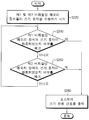
도 5는 도 4의 비휘발성 메모리 시스템의 프로그램 방법에서 제 1 및 제 2 비휘발성 메모리 장치들이 쓰기 동작을 완료하였는지 여부를 판단하는 일 예를 나타내는 순서도이다.
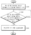
도 6은 도 4의 비휘발성 메모리 시스템의 프로그램 방법에서 제 1 및 제 2 비휘발성 메모리 장치들이 쓰기 동작을 완료하였는지 여부를 판단하는 다른 예를 나타내는 순서도이다.
140: 제 1 비휘발성 메모리 장치 160: 제 2 비휘발성 메모리 장치
Claims (8)
- 제 1 비휘발성 메모리 장치;
상기 제 1 비휘발성 메모리 장치에 비하여 저속으로 쓰기 동작을 수행하고, 상기 제 1 비휘발성 메모리 장치와 이종인 제 2 비휘발성 메모리 장치; 및
쓰기 명령 신호에 기초하여 상기 제 1 및 제 2 비휘발성 메모리 장치들이 호스트(host)로부터 입력되는 데이터에 대한 쓰기 동작을 동시에 수행하도록 제어하고, 상기 제 1 및 제 2 비휘발성 메모리 장치들 중에서 어느 하나가 상기 쓰기 동작을 완료하면, 상기 호스트에 쓰기 완료 신호를 출력하는 컨트롤러를 포함하는 비휘발성 메모리 시스템. - 제 1 항에 있어서, 상기 제 1 비휘발성 메모리 장치가 상기 쓰기 동작을 완료하여 상기 컨트롤러가 상기 쓰기 완료 신호를 출력한 이후에도, 상기 제 2 비휘발성 메모리 장치는 상기 쓰기 동작을 완료하는 것을 특징으로 하는 비휘발성 메모리 시스템.
- 제 2 항에 있어서, 상기 제 2 비휘발성 메모리 장치가 상기 쓰기 동작을 수행하는 도중에 서든 파워 오프(sudden power off)가 발생하면, 상기 제 2 비휘발성 메모리 장치는 상기 제 1 비휘발성 메모리 장치에 쓰여진 상기 데이터에 기초하여 상기 쓰기 동작을 완료하는 것을 특징으로 하는 비휘발성 메모리 시스템.
- 제 1 항에 있어서, 상기 제 1 비휘발성 메모리 장치는 덮어 쓰기 동작(overwrite operation)을 수행할 수 있는 비휘발성 메모리 장치인 것을 특징으로 하는 비휘발성 메모리 시스템.
- 제 4 항에 있어서, 상기 제 1 비휘발성 메모리 장치는 피램(Phase-change Random Access Memory; PRAM) 장치이고, 상기 제 2 비휘발성 메모리 장치는 낸드 플래시 메모리(NAND flash memory) 장치인 것을 특징으로 하는 비휘발성 메모리 시스템.
- 제 5 항에 있어서, 임베디드 멀티미디어 카드(Embedded Multi Media Card; EMMC)로 제조되는 것을 특징으로 하는 비휘발성 메모리 시스템.
- 제 1 항에 있어서, 상기 제 1 및 제 2 비휘발성 메모리 장치들 중에서 어느 하나가 상기 쓰기 동작을 완료하였는지 여부 판단은 폴링 체크(polling check) 방식 또는 라운드 로빈 시그널링(round robin signaling) 방식으로 수행되는 것을 특징으로 하는 비휘발성 메모리 시스템.
- 쓰기 명령 신호에 기초하여 호스트로부터 데이터를 입력받는 단계;
제 1 비휘발성 메모리 장치와 상기 제 1 비휘발성 메모리 장치에 비하여 저속으로 쓰기 동작을 수행하는 제 2 비휘발성 메모리 장치로 하여금 상기 데이터에 대한 쓰기 동작을 동시에 수행시키는 단계;
상기 제 1 및 제 2 비휘발성 메모리 장치가 상기 쓰기 동작을 완료하였는지 여부를 판단하는 단계; 및
상기 제 1 및 제 2 비휘발성 메모리 장치들 중에서 어느 하나가 상기 쓰기 동작을 완료하면 상기 호스트에 쓰기 완료 신호를 출력하는 단계를 포함하는 비휘발성 메모리 시스템의 프로그램 방법.
Priority Applications (3)
| Application Number | Priority Date | Filing Date | Title |
|---|---|---|---|
| KR1020110129661A KR101342658B1 (ko) | 2011-12-06 | 2011-12-06 | 비휘발성 메모리 시스템 및 그 구성 방법 |
| PCT/KR2012/010542 WO2013085305A1 (ko) | 2011-12-06 | 2012-12-06 | 비휘발성 메모리 시스템 및 이를 프로그램하는 방법 |
| US14/362,272 US9286996B2 (en) | 2011-12-06 | 2012-12-06 | Non-volatile memory system and method of programming the same |
Applications Claiming Priority (1)
| Application Number | Priority Date | Filing Date | Title |
|---|---|---|---|
| KR1020110129661A KR101342658B1 (ko) | 2011-12-06 | 2011-12-06 | 비휘발성 메모리 시스템 및 그 구성 방법 |
Publications (2)
| Publication Number | Publication Date |
|---|---|
| KR20130063243A true KR20130063243A (ko) | 2013-06-14 |
| KR101342658B1 KR101342658B1 (ko) | 2013-12-16 |
Family
ID=48574592
Family Applications (1)
| Application Number | Title | Priority Date | Filing Date |
|---|---|---|---|
| KR1020110129661A Active KR101342658B1 (ko) | 2011-12-06 | 2011-12-06 | 비휘발성 메모리 시스템 및 그 구성 방법 |
Country Status (3)
| Country | Link |
|---|---|
| US (1) | US9286996B2 (ko) |
| KR (1) | KR101342658B1 (ko) |
| WO (1) | WO2013085305A1 (ko) |
Families Citing this family (4)
| Publication number | Priority date | Publication date | Assignee | Title |
|---|---|---|---|---|
| KR102413755B1 (ko) | 2015-11-20 | 2022-06-28 | 삼성전자주식회사 | 리텐션 특성에 의한 성능 저하를 복구하는 저장 장치의 동작 방법 및 이를 포함하는 데이터 처리 시스템의 동작 방법 |
| KR20170118284A (ko) | 2016-04-14 | 2017-10-25 | 에스케이하이닉스 주식회사 | 메모리 시스템 및 메모리 시스템의 동작 방법 |
| KR102818468B1 (ko) * | 2020-09-04 | 2025-06-11 | 삼성전자주식회사 | 비휘발성 메모리 패키지 및 이를 포함하는 스토리지 장치 |
| KR20220070989A (ko) | 2020-11-23 | 2022-05-31 | 에스케이하이닉스 주식회사 | 메모리 시스템 및 메모리 시스템의 동작 방법 |
Family Cites Families (9)
| Publication number | Priority date | Publication date | Assignee | Title |
|---|---|---|---|---|
| US7127549B2 (en) * | 2004-02-04 | 2006-10-24 | Sandisk Corporation | Disk acceleration using first and second storage devices |
| JP4662743B2 (ja) * | 2004-09-13 | 2011-03-30 | Necインフロンティア株式会社 | データ2重化システム |
| JP4373943B2 (ja) * | 2005-02-28 | 2009-11-25 | Tdk株式会社 | メモリコントローラ、フラッシュメモリシステム及びフラッシュメモリの制御方法 |
| KR101124504B1 (ko) * | 2005-09-22 | 2012-03-15 | 삼성전자주식회사 | ALD 공정에 의한 비정질 NiO 박막의 제조방법 및상기 비정질 NiO 박막을 이용한 비휘발성 메모리 소자 |
| KR100765786B1 (ko) * | 2006-06-12 | 2007-10-12 | 삼성전자주식회사 | 플래시 메모리 시스템, 그 프로그램을 위한 호스트 시스템및 프로그램 방법 |
| US8140739B2 (en) * | 2008-08-08 | 2012-03-20 | Imation Corp. | Flash memory based storage devices utilizing magnetoresistive random access memory (MRAM) to store files having logical block addresses stored in a write frequency file buffer table |
| JP2010211734A (ja) | 2009-03-12 | 2010-09-24 | Toshiba Storage Device Corp | 不揮発性メモリを用いた記憶装置 |
| TWI451435B (zh) * | 2010-10-08 | 2014-09-01 | Phison Electronics Corp | 非揮發性記憶體儲存裝置、記憶體控制器與資料儲存方法 |
| TWI454922B (zh) * | 2011-12-19 | 2014-10-01 | Phison Electronics Corp | 記憶體儲存裝置及其記憶體控制器與資料寫入方法 |
-
2011
- 2011-12-06 KR KR1020110129661A patent/KR101342658B1/ko active Active
-
2012
- 2012-12-06 WO PCT/KR2012/010542 patent/WO2013085305A1/ko not_active Ceased
- 2012-12-06 US US14/362,272 patent/US9286996B2/en active Active
Also Published As
| Publication number | Publication date |
|---|---|
| US9286996B2 (en) | 2016-03-15 |
| WO2013085305A1 (ko) | 2013-06-13 |
| US20140362648A1 (en) | 2014-12-11 |
| KR101342658B1 (ko) | 2013-12-16 |
Similar Documents
| Publication | Publication Date | Title |
|---|---|---|
| US9483212B2 (en) | Non-volatile memory devices and control methods therefor | |
| TWI703436B (zh) | 資料儲存裝置及其操作方法 | |
| KR102393427B1 (ko) | 반도체장치 및 반도체시스템 | |
| KR102351660B1 (ko) | 전력 관리 메커니즘을 갖는 솔리드 스테이트 메모리 시스템 및 그것의 동작 방법 | |
| KR102211867B1 (ko) | 보조 전원 장치 및 그것을 포함하는 불휘발성 메모리 시스템 | |
| US9304855B2 (en) | Data storage device | |
| KR101431205B1 (ko) | 캐시 메모리 장치 및 캐시 메모리 장치의 데이터 처리 방법 | |
| KR20150044753A (ko) | 데이터 저장 장치의 동작 방법 | |
| US10268540B2 (en) | Data storage device and operating method thereof | |
| US8867283B2 (en) | Semiconductor memory device, operating method thereof, and data storage apparatus including the same | |
| US20240086282A1 (en) | Multi-layer code rate architecture for copyback between partitions with different code rates | |
| US10186302B2 (en) | Semiconductor systems performing double-write operations and methods of operating the same | |
| US10346052B2 (en) | Memory system with priority processing and operating method thereof | |
| KR101342658B1 (ko) | 비휘발성 메모리 시스템 및 그 구성 방법 | |
| KR102729333B1 (ko) | 데이터 저장 장치 및 이를 이용한 스토리지 시스템 | |
| KR102504763B1 (ko) | 데이터 저장 장치 | |
| US12243577B2 (en) | Automated voltage demarcation (VDM) adjustment for memory device | |
| US7885141B2 (en) | Non-volatile memory device and method for setting configuration information thereof | |
| KR102523967B1 (ko) | 데이터 저장 장치 및 그것의 동작 방법 및 그것을 포함하는 데이터 처리 시스템 | |
| CN106201761A (zh) | 数据储存装置及其操作方法 | |
| CN113934562A (zh) | 调整用于数据恢复操作的读取吞吐量层级 | |
| CN112219185B (zh) | 基于与存储器装置相关联的架构而配置的选择组件 | |
| KR102024661B1 (ko) | 불휘발성 메모리 장치 및 그것의 데이터 독출 방법 | |
| KR102766654B1 (ko) | 반도체장치 및 반도체시스템 | |
| KR20150122493A (ko) | 데이터 저장 장치 및 그것의 동작 방법 |
Legal Events
| Date | Code | Title | Description |
|---|---|---|---|
| A201 | Request for examination | ||
| PA0109 | Patent application |
St.27 status event code: A-0-1-A10-A12-nap-PA0109 |
|
| PA0201 | Request for examination |
St.27 status event code: A-1-2-D10-D11-exm-PA0201 |
|
| D13-X000 | Search requested |
St.27 status event code: A-1-2-D10-D13-srh-X000 |
|
| D14-X000 | Search report completed |
St.27 status event code: A-1-2-D10-D14-srh-X000 |
|
| E902 | Notification of reason for refusal | ||
| PE0902 | Notice of grounds for rejection |
St.27 status event code: A-1-2-D10-D21-exm-PE0902 |
|
| T11-X000 | Administrative time limit extension requested |
St.27 status event code: U-3-3-T10-T11-oth-X000 |
|
| AMND | Amendment | ||
| E13-X000 | Pre-grant limitation requested |
St.27 status event code: A-2-3-E10-E13-lim-X000 |
|
| P11-X000 | Amendment of application requested |
St.27 status event code: A-2-2-P10-P11-nap-X000 |
|
| P13-X000 | Application amended |
St.27 status event code: A-2-2-P10-P13-nap-X000 |
|
| PG1501 | Laying open of application |
St.27 status event code: A-1-1-Q10-Q12-nap-PG1501 |
|
| E601 | Decision to refuse application | ||
| PE0601 | Decision on rejection of patent |
St.27 status event code: N-2-6-B10-B15-exm-PE0601 |
|
| AMND | Amendment | ||
| E13-X000 | Pre-grant limitation requested |
St.27 status event code: A-2-3-E10-E13-lim-X000 |
|
| P11-X000 | Amendment of application requested |
St.27 status event code: A-2-2-P10-P11-nap-X000 |
|
| P13-X000 | Application amended |
St.27 status event code: A-2-2-P10-P13-nap-X000 |
|
| PX0901 | Re-examination |
St.27 status event code: A-2-3-E10-E12-rex-PX0901 |
|
| R17-X000 | Change to representative recorded |
St.27 status event code: A-3-3-R10-R17-oth-X000 |
|
| E902 | Notification of reason for refusal | ||
| PE0902 | Notice of grounds for rejection |
St.27 status event code: A-1-2-D10-D21-exm-PE0902 |
|
| PX0701 | Decision of registration after re-examination |
St.27 status event code: A-3-4-F10-F13-rex-PX0701 |
|
| X701 | Decision to grant (after re-examination) | ||
| GRNT | Written decision to grant | ||
| PR0701 | Registration of establishment |
St.27 status event code: A-2-4-F10-F11-exm-PR0701 |
|
| PR1002 | Payment of registration fee |
St.27 status event code: A-2-2-U10-U11-oth-PR1002 Fee payment year number: 1 |
|
| PG1601 | Publication of registration |
St.27 status event code: A-4-4-Q10-Q13-nap-PG1601 |
|
| P14-X000 | Amendment of ip right document requested |
St.27 status event code: A-5-5-P10-P14-nap-X000 |
|
| PN2301 | Change of applicant |
St.27 status event code: A-5-5-R10-R13-asn-PN2301 St.27 status event code: A-5-5-R10-R11-asn-PN2301 |
|
| R18-X000 | Changes to party contact information recorded |
St.27 status event code: A-5-5-R10-R18-oth-X000 |
|
| FPAY | Annual fee payment |
Payment date: 20161209 Year of fee payment: 4 |
|
| PR1001 | Payment of annual fee |
St.27 status event code: A-4-4-U10-U11-oth-PR1001 Fee payment year number: 4 |
|
| R18-X000 | Changes to party contact information recorded |
St.27 status event code: A-5-5-R10-R18-oth-X000 |
|
| FPAY | Annual fee payment |
Payment date: 20171211 Year of fee payment: 5 |
|
| PR1001 | Payment of annual fee |
St.27 status event code: A-4-4-U10-U11-oth-PR1001 Fee payment year number: 5 |
|
| FPAY | Annual fee payment |
Payment date: 20181207 Year of fee payment: 6 |
|
| PR1001 | Payment of annual fee |
St.27 status event code: A-4-4-U10-U11-oth-PR1001 Fee payment year number: 6 |
|
| PR1001 | Payment of annual fee |
St.27 status event code: A-4-4-U10-U11-oth-PR1001 Fee payment year number: 7 |
|
| R18-X000 | Changes to party contact information recorded |
St.27 status event code: A-5-5-R10-R18-oth-X000 |
|
| PR1001 | Payment of annual fee |
St.27 status event code: A-4-4-U10-U11-oth-PR1001 Fee payment year number: 8 |
|
| PR1001 | Payment of annual fee |
St.27 status event code: A-4-4-U10-U11-oth-PR1001 Fee payment year number: 9 |
|
| PR1001 | Payment of annual fee |
St.27 status event code: A-4-4-U10-U11-oth-PR1001 Fee payment year number: 10 |
|
| PR1001 | Payment of annual fee |
St.27 status event code: A-4-4-U10-U11-oth-PR1001 Fee payment year number: 11 |
|
| R18-X000 | Changes to party contact information recorded |
St.27 status event code: A-5-5-R10-R18-oth-X000 |
|
| PN2301 | Change of applicant |
St.27 status event code: A-5-5-R10-R13-asn-PN2301 St.27 status event code: A-5-5-R10-R11-asn-PN2301 |
|
| PR1001 | Payment of annual fee |
St.27 status event code: A-4-4-U10-U11-oth-PR1001 Fee payment year number: 12 |
|
| PR1001 | Payment of annual fee |
St.27 status event code: A-4-4-U10-U11-oth-PR1001 Fee payment year number: 13 |
|
| U11 | Full renewal or maintenance fee paid |
Free format text: ST27 STATUS EVENT CODE: A-4-4-U10-U11-OTH-PR1001 (AS PROVIDED BY THE NATIONAL OFFICE) Year of fee payment: 13 |