KR20130063243A - Non-volatile memory system and method of programming the same - Google Patents
Non-volatile memory system and method of programming the same Download PDFInfo
- Publication number
- KR20130063243A KR20130063243A KR1020110129661A KR20110129661A KR20130063243A KR 20130063243 A KR20130063243 A KR 20130063243A KR 1020110129661 A KR1020110129661 A KR 1020110129661A KR 20110129661 A KR20110129661 A KR 20110129661A KR 20130063243 A KR20130063243 A KR 20130063243A
- Authority
- KR
- South Korea
- Prior art keywords
- nonvolatile memory
- memory device
- write operation
- write
- completed
- Prior art date
- Legal status (The legal status is an assumption and is not a legal conclusion. Google has not performed a legal analysis and makes no representation as to the accuracy of the status listed.)
- Granted
Links
Images


Classifications
-
- G—PHYSICS
- G11—INFORMATION STORAGE
- G11C—STATIC STORES
- G11C16/00—Erasable programmable read-only memories
- G11C16/02—Erasable programmable read-only memories electrically programmable
- G11C16/06—Auxiliary circuits, e.g. for writing into memory
- G11C16/34—Determination of programming status, e.g. threshold voltage, overprogramming or underprogramming, retention
- G11C16/3436—Arrangements for verifying correct programming or erasure
- G11C16/3468—Prevention of overerasure or overprogramming, e.g. by verifying whilst erasing or writing
- G11C16/3486—Circuits or methods to prevent overprogramming of nonvolatile memory cells, e.g. by detecting onset or cessation of current flow in cells and using the detector output to terminate programming
-
- G—PHYSICS
- G11—INFORMATION STORAGE
- G11C—STATIC STORES
- G11C16/00—Erasable programmable read-only memories
- G11C16/02—Erasable programmable read-only memories electrically programmable
- G11C16/06—Auxiliary circuits, e.g. for writing into memory
- G11C16/34—Determination of programming status, e.g. threshold voltage, overprogramming or underprogramming, retention
-
- G—PHYSICS
- G06—COMPUTING OR CALCULATING; COUNTING
- G06F—ELECTRIC DIGITAL DATA PROCESSING
- G06F3/00—Input arrangements for transferring data to be processed into a form capable of being handled by the computer; Output arrangements for transferring data from processing unit to output unit, e.g. interface arrangements
- G06F3/06—Digital input from, or digital output to, record carriers, e.g. RAID, emulated record carriers or networked record carriers
- G06F3/0601—Interfaces specially adapted for storage systems
- G06F3/0602—Interfaces specially adapted for storage systems specifically adapted to achieve a particular effect
- G06F3/061—Improving I/O performance
- G06F3/0611—Improving I/O performance in relation to response time
-
- G—PHYSICS
- G06—COMPUTING OR CALCULATING; COUNTING
- G06F—ELECTRIC DIGITAL DATA PROCESSING
- G06F11/00—Error detection; Error correction; Monitoring
- G06F11/07—Responding to the occurrence of a fault, e.g. fault tolerance
- G06F11/14—Error detection or correction of the data by redundancy in operation
- G06F11/1402—Saving, restoring, recovering or retrying
- G06F11/1415—Saving, restoring, recovering or retrying at system level
- G06F11/1441—Resetting or repowering
-
- G—PHYSICS
- G06—COMPUTING OR CALCULATING; COUNTING
- G06F—ELECTRIC DIGITAL DATA PROCESSING
- G06F11/00—Error detection; Error correction; Monitoring
- G06F11/07—Responding to the occurrence of a fault, e.g. fault tolerance
- G06F11/16—Error detection or correction of the data by redundancy in hardware
- G06F11/1658—Data re-synchronization of a redundant component, or initial sync of replacement, additional or spare unit
-
- G—PHYSICS
- G06—COMPUTING OR CALCULATING; COUNTING
- G06F—ELECTRIC DIGITAL DATA PROCESSING
- G06F11/00—Error detection; Error correction; Monitoring
- G06F11/07—Responding to the occurrence of a fault, e.g. fault tolerance
- G06F11/16—Error detection or correction of the data by redundancy in hardware
- G06F11/1666—Error detection or correction of the data by redundancy in hardware where the redundant component is memory or memory area
-
- G—PHYSICS
- G06—COMPUTING OR CALCULATING; COUNTING
- G06F—ELECTRIC DIGITAL DATA PROCESSING
- G06F12/00—Accessing, addressing or allocating within memory systems or architectures
- G06F12/02—Addressing or allocation; Relocation
- G06F12/0223—User address space allocation, e.g. contiguous or non contiguous base addressing
- G06F12/023—Free address space management
- G06F12/0238—Memory management in non-volatile memory, e.g. resistive RAM or ferroelectric memory
- G06F12/0246—Memory management in non-volatile memory, e.g. resistive RAM or ferroelectric memory in block erasable memory, e.g. flash memory
-
- G—PHYSICS
- G06—COMPUTING OR CALCULATING; COUNTING
- G06F—ELECTRIC DIGITAL DATA PROCESSING
- G06F3/00—Input arrangements for transferring data to be processed into a form capable of being handled by the computer; Output arrangements for transferring data from processing unit to output unit, e.g. interface arrangements
- G06F3/06—Digital input from, or digital output to, record carriers, e.g. RAID, emulated record carriers or networked record carriers
- G06F3/0601—Interfaces specially adapted for storage systems
- G06F3/0602—Interfaces specially adapted for storage systems specifically adapted to achieve a particular effect
- G06F3/061—Improving I/O performance
- G06F3/0613—Improving I/O performance in relation to throughput
-
- G—PHYSICS
- G06—COMPUTING OR CALCULATING; COUNTING
- G06F—ELECTRIC DIGITAL DATA PROCESSING
- G06F3/00—Input arrangements for transferring data to be processed into a form capable of being handled by the computer; Output arrangements for transferring data from processing unit to output unit, e.g. interface arrangements
- G06F3/06—Digital input from, or digital output to, record carriers, e.g. RAID, emulated record carriers or networked record carriers
- G06F3/0601—Interfaces specially adapted for storage systems
- G06F3/0628—Interfaces specially adapted for storage systems making use of a particular technique
- G06F3/0646—Horizontal data movement in storage systems, i.e. moving data in between storage devices or systems
- G06F3/065—Replication mechanisms
-
- G—PHYSICS
- G06—COMPUTING OR CALCULATING; COUNTING
- G06F—ELECTRIC DIGITAL DATA PROCESSING
- G06F3/00—Input arrangements for transferring data to be processed into a form capable of being handled by the computer; Output arrangements for transferring data from processing unit to output unit, e.g. interface arrangements
- G06F3/06—Digital input from, or digital output to, record carriers, e.g. RAID, emulated record carriers or networked record carriers
- G06F3/0601—Interfaces specially adapted for storage systems
- G06F3/0628—Interfaces specially adapted for storage systems making use of a particular technique
- G06F3/0655—Vertical data movement, i.e. input-output transfer; data movement between one or more hosts and one or more storage devices
- G06F3/0659—Command handling arrangements, e.g. command buffers, queues, command scheduling
-
- G—PHYSICS
- G06—COMPUTING OR CALCULATING; COUNTING
- G06F—ELECTRIC DIGITAL DATA PROCESSING
- G06F3/00—Input arrangements for transferring data to be processed into a form capable of being handled by the computer; Output arrangements for transferring data from processing unit to output unit, e.g. interface arrangements
- G06F3/06—Digital input from, or digital output to, record carriers, e.g. RAID, emulated record carriers or networked record carriers
- G06F3/0601—Interfaces specially adapted for storage systems
- G06F3/0668—Interfaces specially adapted for storage systems adopting a particular infrastructure
- G06F3/0671—In-line storage system
- G06F3/0683—Plurality of storage devices
- G06F3/0688—Non-volatile semiconductor memory arrays
-
- G—PHYSICS
- G11—INFORMATION STORAGE
- G11C—STATIC STORES
- G11C14/00—Digital stores characterised by arrangements of cells having volatile and non-volatile storage properties for back-up when the power is down
-
- G—PHYSICS
- G11—INFORMATION STORAGE
- G11C—STATIC STORES
- G11C16/00—Erasable programmable read-only memories
- G11C16/02—Erasable programmable read-only memories electrically programmable
- G11C16/06—Auxiliary circuits, e.g. for writing into memory
- G11C16/10—Programming or data input circuits
-
- G—PHYSICS
- G11—INFORMATION STORAGE
- G11C—STATIC STORES
- G11C16/00—Erasable programmable read-only memories
- G11C16/02—Erasable programmable read-only memories electrically programmable
- G11C16/06—Auxiliary circuits, e.g. for writing into memory
- G11C16/22—Safety or protection circuits preventing unauthorised or accidental access to memory cells
Landscapes
- Engineering & Computer Science (AREA)
- Theoretical Computer Science (AREA)
- Physics & Mathematics (AREA)
- General Engineering & Computer Science (AREA)
- General Physics & Mathematics (AREA)
- Human Computer Interaction (AREA)
- Quality & Reliability (AREA)
- Computer Security & Cryptography (AREA)
- Techniques For Improving Reliability Of Storages (AREA)
Abstract
비휘발성 메모리 시스템은 제 1 비휘발성 메모리 장치, 제 1 비휘발성 메모리 장치에 비하여 저속으로 쓰기 동작을 수행하고 제 1 비휘발성 메모리 장치와 이종인 적어도 하나 이상의 제 2 비휘발성 메모리 장치, 및 쓰기 명령 신호에 기초하여 제 1 및 제 2 비휘발성 메모리 장치들이 호스트로부터 입력되는 데이터에 대한 쓰기 동작을 동시에 수행하도록 제어하고, 제 1 및 제 2 비휘발성 메모리 장치들 중에서 어느 하나가 쓰기 동작을 완료하면, 호스트에 쓰기 완료 신호를 출력하는 컨트롤러를 포함한다. 이에, 비휘발성 메모리 시스템은 고속으로 동작할 수 있고, 서든 파워 오프 발생시 데이터 유실을 방지할 수 있다.The nonvolatile memory system includes a first nonvolatile memory device, at least one second nonvolatile memory device performing a write operation at a low speed compared to the first nonvolatile memory device, and different from the first nonvolatile memory device, and a write command signal. Control the first and second nonvolatile memory devices to simultaneously perform a write operation on data input from the host, and when either one of the first and second nonvolatile memory devices completes the write operation, And a controller that outputs a write completion signal. Thus, the nonvolatile memory system can operate at a high speed, and can prevent data loss when a sudden power off occurs.
Description
본 발명은 반도체 메모리 시스템에 관한 것으로, 보다 상세하게는 이종의 비휘발성 메모리 장치를 구비하는 비휘발성 메모리 시스템 및 이를 프로그램하는 방법에 관한 것이다.The present invention relates to a semiconductor memory system, and more particularly, to a nonvolatile memory system having a heterogeneous nonvolatile memory device and a method of programming the same.
반도체 메모리 장치는 전원이 공급되지 않는 상태에서 데이터를 보존할 수 있는지에 따라 휘발성 메모리 장치와 비휘발성 메모리 장치로 구분될 수 있다. 최근에는, 비휘발성 메모리 장치 중에서 낸드 플래시 메모리 장치가 널리 사용되고 있고, 수 비트의 데이터를 저장할 수 있는 멀티 레벨 셀(Multi Level Cell; MLC)을 포함하여 높은 집적도로 제조되고 있다.The semiconductor memory device may be classified into a volatile memory device and a nonvolatile memory device according to whether data can be stored in a state where power is not supplied. Recently, NAND flash memory devices are widely used among nonvolatile memory devices, and have been manufactured with high density including multi level cells (MLCs) capable of storing several bits of data.
그러나, 낸드 플래시 메모리 장치는 덮어 쓰기가 가능하지 않기 때문에, 쓰기 전 이레이즈 동작(erase before write operation)을 블록 단위로 수행해야 하고, 기 설정된 조건 하에서 유효 데이터(valid data)와 무효 데이터(invalid data)를 분류하여 병합하기 위한 병합 동작(merge operation)을 수행해야 하는 등의 여러 제약을 가지고 있다.However, since the NAND flash memory device cannot be overwritten, an erase before write operation must be performed in units of blocks, and valid data and invalid data must be performed under preset conditions. ) Has several restrictions, such as the need to perform a merge operation to classify and merge).
따라서, 적어도 하나 이상의 낸드 플래시 메모리 장치를 포함하는 반도체 메모리 시스템은 높은 집적도를 가지고 소형으로 제조될 수 있으나, 낸드 플래시 메모리 장치의 여러 제약(예를 들어, 쓰기 동작) 때문에 고속으로 동작할 수 없고, 쓰기 동작 중에 서든 파워 오프(sudden power off)가 발생하면 데이터가 유실된다는 문제점이 있다.Thus, a semiconductor memory system including at least one NAND flash memory device can be manufactured compactly with high density, but cannot operate at high speed due to various limitations (eg, a write operation) of the NAND flash memory device, If sudden power off occurs during a write operation, there is a problem in that data is lost.
본 발명의 일 목적은 이종의 비휘발성 메모리 장치들을 구비하여 고속으로 동작할 수 있고, 서든 파워 오프 발생시 데이터 유실을 방지할 수 있는 비휘발성 메모리 시스템을 제공하는 것이다.One object of the present invention is to provide a nonvolatile memory system having heterogeneous nonvolatile memory devices that can operate at high speed and prevent data loss when sudden power off occurs.
본 발명의 다른 목적은 상기 비휘발성 메모리 시스템을 프로그램하는 방법을 제공하는 것이다.Another object of the present invention is to provide a method of programming the nonvolatile memory system.
다만, 본 발명의 해결하고자 하는 과제는 이에 한정되는 것이 아니며, 본 발명의 사상 및 영역으로부터 벗어나지 않는 범위에서 다양하게 확장될 수 있을 것이다.It should be understood, however, that the present invention is not limited to the above-described embodiments, but may be variously modified without departing from the spirit and scope of the invention.
본 발명의 일 목적을 달성하기 위하여, 본 발명의 실시예들에 따른 비휘발성 메모리 시스템은 제 1 비휘발성 메모리 장치, 상기 제 1 비휘발성 메모리 장치에 비하여 저속으로 쓰기 동작을 수행하고 상기 제 1 비휘발성 메모리 장치와 이종인(heterogeneous) 제 2 비휘발성 메모리 장치, 및 쓰기 명령 신호에 기초하여 상기 제 1 및 제 2 비휘발성 메모리 장치들이 호스트(host)로부터 입력되는 데이터에 대한 쓰기 동작을 동시에 수행하도록 제어하고, 상기 제 1 및 제 2 비휘발성 메모리 장치들 중에서 어느 하나가 상기 쓰기 동작을 완료하면, 상기 호스트에 쓰기 완료 신호를 출력하는 컨트롤러를 포함할 수 있다.In order to achieve the object of the present invention, the nonvolatile memory system according to the embodiments of the present invention performs a write operation at a low speed compared to the first nonvolatile memory device, the first nonvolatile memory device and the first nonvolatile memory system. Control the first and second nonvolatile memory devices to simultaneously perform a write operation on data input from a host based on a volatile memory device, a heterogeneous second nonvolatile memory device, and a write command signal The controller may include a controller configured to output a write completion signal to the host when any one of the first and second nonvolatile memory devices completes the write operation.
일 실시예에 의하면, 상기 제 1 비휘발성 메모리 장치가 상기 쓰기 동작을 완료하여 상기 컨트롤러가 상기 쓰기 완료 신호를 출력한 이후에도, 상기 제 2 비휘발성 메모리 장치는 상기 쓰기 동작을 완료할 수 있다.According to an embodiment, even after the first nonvolatile memory device completes the write operation and the controller outputs the write completion signal, the second nonvolatile memory device may complete the write operation.
일 실시예에 의하면, 상기 제 2 비휘발성 메모리 장치가 상기 쓰기 동작을 수행하는 도중에 서든 파워 오프(sudden power off)가 발생하면, 상기 제 2 비휘발성 메모리 장치는 상기 제 1 비휘발성 메모리 장치에 쓰여진 상기 데이터에 기초하여 상기 쓰기 동작을 완료할 수 있다.In example embodiments, when a sudden power off occurs while the second nonvolatile memory device is performing the write operation, the second nonvolatile memory device is written to the first nonvolatile memory device. The write operation may be completed based on the data.
일 실시예에 의하면, 상기 제 1 비휘발성 메모리 장치는 덮어 쓰기 동작(overwrite operation)을 수행할 수 있는 비휘발성 메모리 장치일 수 있다.In example embodiments, the first nonvolatile memory device may be a nonvolatile memory device capable of performing an overwrite operation.
일 실시예에 의하면, 상기 제 1 비휘발성 메모리 장치는 피램(Phase-change Random Access Memory; PRAM) 장치이고, 상기 제 2 비휘발성 메모리 장치는 낸드 플래시 메모리(NAND flash memory) 장치일 수 있다.In example embodiments, the first nonvolatile memory device may be a phase-change random access memory (PRAM) device, and the second nonvolatile memory device may be a NAND flash memory device.
일 실시예에 의하면, 상기 비휘발성 메모리 시스템은 임베디드 멀티 미디어 카드(Embedded Multi Media Card; EMMC)로 제조될 수 있다.In example embodiments, the nonvolatile memory system may be manufactured as an embedded multi-media card (EMMC).
일 실시예에 의하면, 상기 제 1 및 제 2 비휘발성 메모리 장치들 중에서 어느 하나가 상기 쓰기 동작을 완료하였는지 여부 판단은 폴링 체크(polling check) 방식 또는 라운드 로빈 시그널링(round robin signaling) 방식으로 수행될 수 있다.According to an embodiment, determining whether one of the first and second nonvolatile memory devices has completed the write operation may be performed by a polling check method or a round robin signaling method. Can be.
본 발명의 다른 목적을 달성하기 위하여, 본 발명의 실시예들에 따른 비휘발성 메모리 시스템의 프로그램 방법은 쓰기 명령 신호에 기초하여 호스트로부터 데이터를 입력받는 단계, 제 1 비휘발성 메모리 장치와 상기 제 1 비휘발성 메모리 장치에 비하여 저속으로 쓰기 동작을 수행하는 제 2 비휘발성 메모리 장치로 하여금 상기 데이터에 대한 쓰기 동작을 동시에 수행시키는 단계, 상기 제 1 및 제 2 비휘발성 메모리 장치가 상기 쓰기 동작을 완료하였는지 여부를 판단하는 단계, 및 상기 제 1 및 제 2 비휘발성 메모리 장치들 중에서 어느 하나가 상기 쓰기 동작을 완료하면 상기 호스트에 쓰기 완료 신호를 출력하는 단계를 포함할 수 있다.In accordance with another aspect of the present invention, a program method of a nonvolatile memory system according to an embodiment of the present invention includes receiving data from a host based on a write command signal, a first nonvolatile memory device and the first method. Simultaneously performing a write operation on the data by a second nonvolatile memory device performing a write operation at a lower speed than that of the nonvolatile memory device, and whether the first and second nonvolatile memory devices have completed the write operation. The method may include determining whether or not, and if one of the first and second nonvolatile memory devices completes the write operation, outputting a write completion signal to the host.
본 발명의 실시예들에 따른 비휘발성 메모리 시스템 및 이의 프로그램 방법은 호스트로부터 입력되는 데이터에 대한 쓰기 동작을 이종의 비휘발성 메모리 장치들이 동시에 수행하게 하고, 이종의 비휘발성 메모리 장치들 중에서 어느 하나의 쓰기 동작이 완료하면 호스트에 쓰기 완료 신호가 출력되게 함으로써, 사용자로 하여금 고속으로 동작하는 것과 같이 느끼게 할 수 있고, 서든 파워 오프 발생시 이종의 비휘발성 메모리 장치들에 쓰여진 데이터를 서로 비교하여 유실된 데이터를 복구시킬 수 있다. 다만, 본 발명의 효과는 이에 한정되는 것이 아니며, 본 발명의 사상 및 영역으로부터 벗어나지 않는 범위에서 다양하게 확장될 수 있을 것이다.A nonvolatile memory system and a program method thereof according to embodiments of the present invention allow a heterogeneous nonvolatile memory device to simultaneously perform a write operation on data input from a host, and the nonvolatile memory device may execute any one of heterogeneous nonvolatile memory devices. When the write operation is completed, the write completion signal is output to the host, so that the user can feel as if the user is operating at high speed. Can be restored. However, the effects of the present invention are not limited thereto, and various modifications may be made without departing from the spirit and scope of the present invention.
도 1은 본 발명의 실시예들에 따른 비휘발성 메모리 시스템을 나타내는 블록도이다.
도 2a 내지 도 2c는 도 1의 비휘발성 메모리 시스템에서 데이터에 대한 쓰기 동작이 수행되는 일 예를 나타내는 도면들이다.
도 3a 내지 도 3d는 도 1의 비휘발성 메모리 시스템에서 데이터에 대한 복구 동작이 수행되는 일 예를 나타내는 도면들이다.
도 4는 본 발명의 실시예들에 따른 비휘발성 메모리 시스템의 프로그램 방법을 나타내는 순서도이다.
도 5는 도 4의 비휘발성 메모리 시스템의 프로그램 방법에서 제 1 및 제 2 비휘발성 메모리 장치들이 쓰기 동작을 완료하였는지 여부를 판단하는 일 예를 나타내는 순서도이다.
도 6은 도 4의 비휘발성 메모리 시스템의 프로그램 방법에서 제 1 및 제 2 비휘발성 메모리 장치들이 쓰기 동작을 완료하였는지 여부를 판단하는 다른 예를 나타내는 순서도이다.1 is a block diagram illustrating a non-volatile memory system in accordance with embodiments of the present invention.
2A through 2C are diagrams illustrating an example of performing a write operation on data in the nonvolatile memory system of FIG. 1.
3A to 3D are diagrams illustrating an example of performing a recovery operation on data in the nonvolatile memory system of FIG. 1.
4 is a flowchart illustrating a program method of a nonvolatile memory system according to example embodiments.
FIG. 5 is a flowchart illustrating an example of determining whether first and second nonvolatile memory devices have completed a write operation in the program method of the nonvolatile memory system of FIG. 4.
6 is a flowchart illustrating another example of determining whether first and second nonvolatile memory devices have completed a write operation in the program method of the nonvolatile memory system of FIG. 4.
본문에 개시되어 있는 본 발명의 실시예들에 대해서, 특정한 구조적 내지 기능적 설명들은 단지 본 발명의 실시예를 설명하기 위한 목적으로 예시된 것으로, 본 발명의 실시예들은 다양한 형태로 실시될 수 있으며 본문에 설명된 실시예들에 한정되는 것으로 해석되어서는 아니 된다.For the embodiments of the invention disclosed herein, specific structural and functional descriptions are set forth for the purpose of describing an embodiment of the invention only, and it is to be understood that the embodiments of the invention may be practiced in various forms, The present invention should not be construed as limited to the embodiments described in Figs.
본 발명은 다양한 변경을 가할 수 있고 여러 가지 형태를 가질 수 있는바, 특정 실시예들을 도면에 예시하고 본문에 상세하게 설명하고자 한다. 그러나 이는 본 발명을 특정한 개시 형태에 대해 한정하려는 것이 아니며, 본 발명의 사상 및 기술 범위에 포함되는 모든 변경, 균등물 내지 대체물을 포함하는 것으로 이해되어야 한다.As the inventive concept allows for various changes and numerous modifications, particular embodiments will be illustrated in the drawings and described in detail in the text. It is to be understood, however, that the invention is not intended to be limited to the particular forms disclosed, but on the contrary, is intended to cover all modifications, equivalents, and alternatives falling within the spirit and scope of the invention.
제 1, 제 2 등의 용어는 다양한 구성요소들을 설명하는데 사용될 수 있지만, 상기 구성요소들은 상기 용어들에 의해 한정되어서는 안 된다. 상기 용어들은 하나의 구성요소를 다른 구성요소로부터 구별하는 목적으로 사용될 수 있다. 예를 들어, 본 발명의 권리 범위로부터 이탈되지 않은 채 제 1 구성요소는 제 2 구성요소로 명명될 수 있고, 유사하게 제 2 구성요소도 제 1 구성요소로 명명될 수 있다.Terms such as first and second may be used to describe various components, but the components should not be limited by the terms. The terms may be used for the purpose of distinguishing one component from another component. For example, without departing from the scope of the present invention, the first component may be referred to as a second component, and similarly, the second component may also be referred to as a first component.
어떤 구성요소가 다른 구성요소에 "연결되어" 있다거나 "접속되어" 있다고 언급된 때에는, 그 다른 구성요소에 직접적으로 연결되어 있거나 또는 접속되어 있을 수도 있지만, 중간에 다른 구성요소가 존재할 수도 있다고 이해되어야 할 것이다. 반면에, 어떤 구성요소가 다른 구성요소에 "직접 연결되어" 있다거나 "직접 접속되어" 있다고 언급된 때에는, 중간에 다른 구성요소가 존재하지 않는 것으로 이해되어야 할 것이다. 구성요소들 간의 관계를 설명하는 다른 표현들, 즉 "~사이에"와 "바로 ~사이에" 또는 "~에 이웃하는"과 "~에 직접 이웃하는" 등도 마찬가지로 해석되어야 한다.When a component is referred to as being "connected" or "connected" to another component, it may be directly connected to or connected to that other component, but it may be understood that other components may be present in between. Should be. On the other hand, when an element is referred to as being "directly connected" or "directly connected" to another element, it should be understood that there are no other elements in between. Other expressions describing the relationship between components, such as "between" and "immediately between," or "neighboring to," and "directly neighboring to" should be interpreted as well.
본 출원에서 사용한 용어는 단지 특정한 실시예를 설명하기 위해 사용된 것으로, 본 발명을 한정하려는 의도가 아니다. 단수의 표현은 문맥상 명백하게 다르게 뜻하지 않는 한, 복수의 표현을 포함한다. 본 출원에서, "포함하다" 또는 "가지다" 등의 용어는 설시된 특징, 숫자, 단계, 동작, 구성요소, 부분품 또는 이들을 조합한 것이 존재함을 지정하려는 것이지, 하나 또는 그 이상의 다른 특징들이나 숫자, 단계, 동작, 구성요소, 부분품 또는 이들을 조합한 것들의 존재 또는 부가 가능성을 미리 배제하지 않는 것으로 이해되어야 한다.The terminology used herein is for the purpose of describing particular example embodiments only and is not intended to be limiting of the present invention. Singular expressions include plural expressions unless the context clearly indicates otherwise. In the present application, the terms "comprise", "having", and the like are intended to specify the presence of stated features, integers, steps, operations, elements, components, or combinations thereof, , Steps, operations, components, parts, or combinations thereof, as a matter of principle.
다르게 정의되지 않는 한, 기술적이거나 과학적인 용어를 포함해서 여기서 사용되는 모든 용어들은 본 발명이 속하는 기술분야에서 통상의 지식을 가진 자에 의해 일반적으로 이해되는 것과 동일한 의미이다. 일반적으로 사용되는 사전에 정의되어 있는 것과 같은 용어들은 관련 기술의 문맥상 가지는 의미와 일치하는 의미인 것으로 해석되어야 하며, 본 출원에서 명백하게 정의하지 않는 한, 이상적이거나 과도하게 형식적인 의미로 해석되지 않는다.Unless otherwise defined, all terms used herein, including technical or scientific terms, have the same meaning as commonly understood by one of ordinary skill in the art to which this invention belongs. Terms such as those defined in commonly used dictionaries should be construed as meaning consistent with meaning in the context of the relevant art and are not to be construed as ideal or overly formal in meaning unless expressly defined in the present application .
이하, 첨부한 도면들을 참조하여, 본 발명의 바람직한 실시예를 보다 상세하게 설명하고자 한다. 도면상의 동일한 구성요소에 대해서는 동일한 참조부호를 사용하고 동일한 구성요소에 대해서 중복된 설명은 생략한다.Hereinafter, with reference to the accompanying drawings, it will be described in detail a preferred embodiment of the present invention. The same reference numerals are used for the same constituent elements in the drawings and redundant explanations for the same constituent elements are omitted.
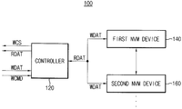
도 1은 본 발명의 실시예들에 따른 비휘발성 메모리 시스템을 나타내는 블록도이다.1 is a block diagram illustrating a non-volatile memory system in accordance with embodiments of the present invention.
도 1을 참조하면, 비휘발성 메모리 시스템(100)은 컨트롤러(120), 제 1 비휘발성 메모리 장치(140) 및 제 2 비휘발성 메모리 장치(160)를 포함할 수 있다. 도 1에서는 1개의 제 1 비휘발성 메모리 장치(140)와 1개의 제 2 비휘발성 메모리 장치(160)가 도시되었지만, 이것은 설명의 편의를 위한 것으로서, 비휘발성 메모리 시스템(100)은 적어도 하나 이상의 제 1 비휘발성 메모리 장치(140)와 적어도 하나 이상의 제 2 비휘발성 메모리 장치(160)를 포함하는 것으로 해석되어야 할 것이다.Referring to FIG. 1, the
제 1 비휘발성 메모리 장치(140)는 쓰기 동작이 고속으로 수행되는 비휘발성 메모리 장치일 수 있고, 제 2 비휘발성 메모리 장치(160)는 쓰기 동작이 저속으로 수행되는 비휘발성 메모리 장치일 수 있다. 즉, 제 1 비휘발성 메모리 장치(140)와 제 2 비휘발성 메모리 장치(160)는 이종의 비휘발성 메모리 장치들에 해당한다. 이 때, 제 1 비휘발성 메모리 장치(140)는 제 2 비휘발성 메모리 장치(160)의 쓰기 동작을 보완하기 위한 것으로서, 호스트(host)로부터 입력되는 데이터(WDAT)는 최종적으로 제 2 비휘발성 메모리 장치(160)에 저장되는 것이다. 따라서, 제 1 비휘발성 메모리 장치(140)는 제 2 비휘발성 메모리 장치(160)에 비하여 쓰기 동작을 고속으로 수행하지만, 저용량의 저장 공간을 가질 수 있다. 그 결과, 비휘발성 메모리 시스템(100)은 저용량의 저장 공간을 갖는 제 1 비휘발성 메모리 장치(140)를 구비함으로써 저비용으로 제조될 수 있고, 고속으로 쓰기 동작을 수행하는 제 1 비휘발성 메모리 장치(140)로 하여금 제 2 비휘발성 메모리 장치(160)의 쓰기 동작을 보완하게 할 수 있다. 일 실시예에서, 제 1 비휘발성 메모리 장치(140)는 고속으로 쓰기 동작을 수행해야 하므로 덮어 쓰기 동작(overwrite operation)을 수행할 수 있는 비휘발성 메모리 장치로 선택될 수 있고, 제 2 비휘발성 메모리 장치(160)는 소형으로 제조되면서도 대용량의 저장 공간을 가질 수 있는 비휘발성 메모리 장치로 선택될 수 있다. 예를 들어, 제 1 비휘발성 메모리 장치(140)는 피램(Phase-change Random Access Memory; PRAM) 장치로 선택될 수 있고, 제 2 비휘발성 메모리 장치(160)는 낸드 플래시 메모리(NAND flash memory) 장치로 선택될 수 있다. 다만, 이것은 하나의 예시로서 제 1 및 제 2 비휘발성 메모리 장치들(140, 160)의 종류가 이에 한정되지는 않는다.The first
컨트롤러(120)는 쓰기 명령 신호(WCMD)에 기초하여 제 1 및 제 2 비휘발성 메모리 장치들(140, 160)이 호스트로부터 입력되는 데이터(WDAT)에 대한 쓰기 동작을 동시에 수행하도록 제어하고, 제 1 및 제 2 비휘발성 메모리 장치들(140, 160) 중에서 어느 하나가 쓰기 동작을 완료하면 호스트에 쓰기 완료 신호(WCS)를 출력할 수 있다. 상술한 바와 같이, 제 1 비휘발성 메모리 장치(140)가 고속으로 쓰기 동작을 수행하는 비휘발성 메모리 장치로 선택되고, 제 2 비휘발성 메모리 장치(160)가 저속으로 쓰기 동작을 수행하는 비휘발성 메모리 장치로 선택되기 때문에, 제 1 비휘발성 메모리 장치(140)가 제 2 비휘발성 메모리 장치(160)에 비해 쓰기 동작을 먼저 완료하는 것이 일반적이다. 그러나, 데이터 패턴에 따라 제 1 비휘발성 메모리 장치(140)보다 제 2 비휘발성 메모리 장치(160)가 쓰기 동작을 먼저 완료할 수도 있는 것이므로, 본 발명은 제 2 비휘발성 메모리 장치(160)가 제 1 비휘발성 메모리 장치(140)보다 쓰기 동작을 먼저 완료하는 경우를 배제하지 않는다. 다만, 제 1 비휘발성 메모리 장치(140)가 제 2 비휘발성 메모리 장치(160)보다 쓰기 동작을 먼저 완료하는 경우가 일반적임을 고려할 때, 비휘발성 메모리 시스템(100)에서는 제 1 비휘발성 메모리 장치(140)가 쓰기 동작을 완료함으로써, 컨트롤러(120)가 쓰기 완료 신호(WCMD)를 출력한 이후에도, 제 2 비휘발성 메모리 장치(160)는 쓰기 동작을 계속 수행하여 완료한다.The
이와 같이, 비휘발성 메모리 시스템(100)에서는 제 1 비휘발성 메모리 장치(140)가 먼저 쓰기 동작을 완료하면, 컨트롤러(120)가 쓰기 완료 신호(WCMD)를 출력하여, 사용자로 하여금 비휘발성 메모리 시스템(100)이 고속으로 동작하는 것과 같이 느끼게 할 수 있다. 이 때, 사용자는 다음 쓰기 동작을 준비(예를 들어, 데이터 프로세싱 시간, 데이터 트랜스퍼 시간 등)할 것이므로, 그 사이에 제 2 비휘발성 메모리 장치(160)는 쓰기 동작을 완료할 수 있다. 그 결과, 비휘발성 메모리 시스템(100)은 실질적으로 제 1 비휘발성 메모리 장치(140)의 쓰기 동작 속도에 상응하는 쓰기 동작 속도로 쓰기 동작을 수행할 수 있다. 그러나, 컨트롤러(120)가 쓰기 완료 신호(WCMD)를 출력한 이후, 제 2 비휘발성 메모리 장치(160)가 쓰기 동작을 완료하기 전에, 서든 파워 오프(sudden power off)가 발생할 수 있다. 이러한 경우, 상기 데이터(WDAT)는 제 2 비휘발성 메모리 장치(160)에 저장되지 않은 채 유실될 수 있다. 이에, 비휘발성 메모리 시스템(100)에서는 제 2 비휘발성 메모리 장치(160)가 쓰기 동작을 수행하는 도중에 서든 파워 오프가 발생하면, 컨트롤러(120)가 제 2 비휘발성 메모리 장치(160)로 하여금 제 1 비휘발성 메모리 장치(140)에 쓰여진 데이터(WDAT)에 기초하여 쓰기 동작을 완료하게 할 수 있다. 나아가, 컨트롤러(120)는 기 설정된 주기 또는 외부 커맨드에 따라 제 1 비휘발성 메모리 장치(140)와 제 2 비휘발성 메모리 장치(160)를 스캐닝(scanning) 및 비교함으로써 상기 데이터(WDAT)를 복구시키는 기능 등도 제공할 수 있다. 이에, 비휘발성 메모리 시스템(100)은 높은 동작 안정성을 확보할 수 있다.As described above, in the
한편, 제 1 비휘발성 메모리 장치(140)가 제 2 비휘발성 메모리 장치(160)보다 쓰기 동작을 먼저 완료하는 경우가 일반적이긴 하지만, 데이터 패턴에 따라 제 1 비휘발성 메모리 장치(140)보다 제 2 비휘발성 메모리 장치(160)가 쓰기 동작을 먼저 완료할 수도 있는 것이므로, 컨트롤러(120)는 제 1 및 제 2 비휘발성 메모리 장치들(120, 140) 중에서 어느 하나가 쓰기 동작을 완료하였는지 여부를 판단해야 한다. 이 때, 제 1 및 제 2 비휘발성 메모리 장치들(120, 140)의 쓰기 동작이 완료되었는지는 폴링 체크(polling check) 방식 또는 라운드 로빈 시그널링(round robin signaling) 방식으로 수행될 수 있다. 다만, 상기 방식들 자체는 해당 기술 분야에서 널리 사용되고 있는 것이므로, 그에 대한 구체적인 설명은 생략하기로 한다. 비휘발성 메모리 시스템(100)에서는 상기 쓰기 동작으로 제 2 비휘발성 메모리 장치(160)에 데이터(WDAT)가 저장되면, 독출 명령 신호(미도시)에 기초하여 제 2 비휘발성 메모리 장치(160)로부터 데이터(RDAT)를 독출하여 호스트에 제공할 수 있다. 이와 같이, 비휘발성 메모리 시스템(100)은 호스트로부터 입력되는 데이터(WDAT)에 대한 쓰기 동작을 이종의 비휘발성 메모리 장치들(140, 160)이 동시에 수행하게 하고, 이종의 비휘발성 메모리 장치들(140, 160) 중에서 어느 하나의 쓰기 동작이 완료하면 호스트에 쓰기 완료 신호(WCS)가 출력되게 함으로써, 사용자로 하여금 고속으로 동작하는 것과 같이 느끼게 할 수 있고, 서든 파워 오프 발생시 이종의 비휘발성 메모리 장치들(140, 160)에 쓰여진 데이터를 서로 비교하여 유실된 데이터를 복구시킬 수 있다. 이 때, 비휘발성 메모리 시스템(100)은 임베디드 멀티미디어 카드(Embedded Multi-Media Card; EMMC)로 제조될 수 있으나, 그에 한정되는 것은 아니다. 예를 들어, 비휘발성 메모리 시스템(100)은 SD 카드(secure digital card), CF 카드(compact flash card), 메모리 스틱(memory stick), XD 픽쳐 카드(XD picture card) 등으로도 제조될 수 있다.Meanwhile, although the first
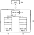
도 2a 내지 도 2c는 도 1의 비휘발성 메모리 시스템에서 데이터에 대한 쓰기 동작이 수행되는 일 예를 나타내는 도면들이다.2A through 2C are diagrams illustrating an example of performing a write operation on data in the nonvolatile memory system of FIG. 1.
도 2a 내지 도 2c를 참조하면, 도 2a는 컨트롤러(120)가 쓰기 명령 신호(WCMD)에 기초하여 제 1 및 제 2 비휘발성 메모리 장치들(140, 160)에 호스트(200)로부터 입력되는 데이터(WDAT)를 제공하는 것을 보여주고 있다. 이에, 제 1 및 제 2 비휘발성 메모리 장치들(140, 160) 각각은 상기 데이터(예를 들어, A)에 대한 쓰기 동작을 동시에 수행할 수 있다. 도 2b는 제 1 및 제 2 비휘발성 메모리 장치들(140, 160) 중에서 어느 하나가 쓰기 동작을 완료하는 것을 보여주고 있다. 이 때, 제 1 비휘발성 메모리 장치(140)는 고속으로 쓰기 동작을 수행할 수 있고, 제 2 비휘발성 메모리 장치(160)는 저속으로 쓰기 동작을 수행할 수 있으므로, 제 1 비휘발성 메모리 장치(140)가 먼저 쓰기 동작을 완료하는 것이 일반적이다. 그러나, 데이터 패턴에 따라 제 2 비휘발성 메모리 장치(160)가 제 1 비휘발성 메모리 장치(140)보다 쓰기 동작을 먼저 완료할 수도 있다. 다만, 도 2b에서는 제 1 비휘발성 메모리 장치(140)가 제 2 비휘발성 메모리 장치(160)보다 쓰기 동작을 먼저 완료하고, 쓰기 동작이 완료되었음을 나타내는 신호(COMP)를 컨트롤러(120)에 제공하는 것이 도시되어 있다. 이 때, 제 1 및 제 2 비휘발성 메모리 장치들(140, 160) 중에서 어느 하나가 쓰기 동작을 완료하였는지 여부 판단은 폴링 체크 방식 또는 라운드 로빈 시그널링 방식으로 수행될 수 있으므로, 쓰기 동작이 완료되었음을 나타내는 신호(COMP)는 제 1 및 제 2 비휘발성 메모리 장치들(140, 160)에서 쓰기 동작이 완료되었는지 여부를 판단하기 위한 다양한 신호들로 해석될 수 있다. 도 2c는 제 1 비휘발성 메모리 장치(140)가 쓰기 동작을 완료하여 컨트롤러(120)가 호스트(200)에 쓰기 완료 신호(WCS)를 출력한 이후에도, 제 2 비휘발성 메모리 장치(160)가 쓰기 동작을 계속 수행하여 완료하는 것을 보여주고 있다. 즉, 사용자가 다음 쓰기 동작을 준비(예를 들어, 데이터 프로세싱 시간, 데이터 트랜스퍼 시간 등)하는 동안에, 제 2 비휘발성 메모리 장치(160)는 쓰기 동작을 중단하지 않고 계속 수행하여 완료하는 것이다. 이는 호스트(host)로부터 입력되는 데이터(WDAT)는 최종적으로 제 2 비휘발성 메모리 장치(160)에 저장되어야 하기 때문이다. 이와 같이, 비휘발성 메모리 시스템(100)에서 제 1 비휘발성 메모리 장치(140)가 제 2 비휘발성 메모리 장치(160)의 쓰기 동작을 보완하고 있으므로, 비휘발성 메모리 시스템(100)은 사용자로 하여금 고속으로 동작하는 것과 같이 느끼게 할 수 있다.Referring to FIGS. 2A through 2C, FIG. 2A illustrates data input from the
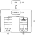
도 3a 내지 도 3d는 도 1의 비휘발성 메모리 시스템에서 데이터에 대한 복구 동작이 수행되는 일 예를 나타내는 도면들이다.3A to 3D are diagrams illustrating an example of performing a recovery operation on data in the nonvolatile memory system of FIG. 1.
도 3a 내지 도 3d를 참조하면, 도 3a는 컨트롤러(120)가 쓰기 명령 신호(WCMD)에 기초하여 제 1 및 제 2 비휘발성 메모리 장치들(140, 160)에 호스트(200)로부터 입력되는 데이터(WDAT)를 제공하는 것을 보여주고 있다. 이에, 제 1 및 제 2 비휘발성 메모리 장치들(140, 160) 각각은 상기 데이터(예를 들어, B)에 대한 쓰기 동작을 동시에 수행할 수 있다. 도 3b는 제 1 및 제 2 비휘발성 메모리 장치들(140, 160) 중에서 제 1 비휘발성 메모리 장치(140)가 쓰기 동작을 먼저 완료하고, 쓰기 동작이 완료되었음을 나타내는 신호(COMP)를 컨트롤러(120)에 제공하는 것을 보여주고 있다. 다만, 제 1 및 제 2 비휘발성 메모리 장치들(140, 160) 중에서 어느 하나가 쓰기 동작을 완료하였는지 여부 판단은 폴링 체크 방식 또는 라운드 로빈 시그널링 방식으로 수행될 수 있으므로, 쓰기 동작이 완료되었음을 나타내는 신호(COMP)는 제 1 및 제 2 비휘발성 메모리 장치들(140, 160)에서 쓰기 동작이 완료되었는지 여부를 판단하기 위한 다양한 신호들로 해석될 수 있다. 한편, 도 3c는 제 2 비휘발성 메모리 장치(160)가 쓰기 동작을 수행하는 도중에 서든 파워 오프가 발생하는 것을 보여주고 있다. 이 때, 쓰기 완료 신호(WCS)가 호스트(200)에 출력된 이후이므로, 호스트(200)가 제 2 비휘발성 메모리 장치(160)의 상기 데이터(예를 들어, B)를 독출하려고 하는 경우, 그에 따른 에러가 발생할 수 있다. 이에, 도 3d에 도시된 바와 같이, 제 2 비휘발성 메모리 장치(160)는 제 1 비휘발성 메모리 장치(140)에 쓰여진 상기 데이터(예를 들어, B)에 기초하여 쓰기 동작을 완료할 수 있다. 이와 같이, 비휘발성 메모리 시스템(100)은 서든 파워 오프 발생시 이종의 비휘발성 메모리 장치들(140, 160)에 쓰여진 데이터를 서로 비교하여 유실된 데이터를 복구함으로써 높은 동작 안정성을 확보할 수 있다.3A to 3D, FIG. 3A illustrates data input from the
도 4는 본 발명의 실시예들에 따른 비휘발성 메모리 시스템의 프로그램 방법을 나타내는 순서도이고, 도 5는 도 4의 비휘발성 메모리 시스템의 프로그램 방법에서 제 1 및 제 2 비휘발성 메모리 장치들이 쓰기 동작을 완료하였는지 여부를 판단하는 일 예를 나타내는 순서도이며, 도 6은 도 4의 비휘발성 메모리 시스템의 프로그램 방법에서 제 1 및 제 2 비휘발성 메모리 장치들이 쓰기 동작을 완료하였는지 여부를 판단하는 다른 예를 나타내는 순서도이다.4 is a flowchart illustrating a program method of a nonvolatile memory system according to example embodiments. FIG. 5 is a diagram illustrating a write operation of first and second nonvolatile memory devices in the program method of the nonvolatile memory system of FIG. 4. FIG. 6 is a flowchart illustrating an example of determining whether the data has been completed, and FIG. 6 illustrates another example of determining whether the first and second nonvolatile memory devices have completed a write operation in the program method of the nonvolatile memory system of FIG. 4. Flowchart.
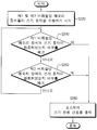
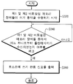
도 4를 참조하면, 본 발명의 실시예들에 따른 비휘발성 메모리 시스템의 프로그램 방법은 쓰기 명령 신호에 기초하여 호스트로부터 데이터를 입력(Step S120)받고, 제 1 비휘발성 메모리 장치와 제 1 비휘발성 메모리 장치에 비하여 저속으로 쓰기 동작을 수행하는 제 2 비휘발성 메모리 장치로 하여금 상기 데이터에 대한 쓰기 동작을 동시에 수행하도록 제어(Step S140)하며, 제 1 및 제 2 비휘발성 메모리 장치가 쓰기 동작을 완료하였는지 여부를 판단(Step S160)하여, 제 1 및 제 2 비휘발성 메모리 장치들 중에서 어느 하나가 쓰기 동작을 완료하면 호스트에 쓰기 완료 신호를 출력(Step S180)할 수 있다. 다만, 이에 대해서는 상술한 바 있으므로, 그에 대한 중복되는 설명은 생략하기로 한다. 한편, 본 발명의 실시예들에 따른 비휘발성 메모리 시스템의 프로그램 방법은 제 1 및 제 2 비휘발성 메모리 장치들이 쓰기 동작을 완료하였는지 여부를 다양한 방식으로 판단할 수 있다. 예를 들어, 제 1 및 제 2 비휘발성 메모리 장치들 중에서 어느 하나가 쓰기 동작을 완료하였는지 여부 판단은 폴링 체크 방식 또는 라운드 로빈 시그널링 방식으로 수행될 수 있다.Referring to FIG. 4, a program method of a nonvolatile memory system according to example embodiments of the inventive concepts receives data from a host based on a write command signal (Step S120), and includes a first nonvolatile memory device and a first nonvolatile memory. A second nonvolatile memory device performing a write operation at a low speed compared to the memory device is controlled to simultaneously perform a write operation on the data (Step S140), and the first and second nonvolatile memory devices complete the write operation. In operation S160, when one of the first and second nonvolatile memory devices completes the write operation, a write completion signal may be output to the host (Step S180). However, since this has been described above, a duplicate description thereof will be omitted. Meanwhile, the program method of the nonvolatile memory system according to the embodiments of the present invention may determine whether the first and second nonvolatile memory devices have completed a write operation in various ways. For example, whether one of the first and second nonvolatile memory devices has completed a write operation may be performed by a polling check method or a round robin signaling method.
일 실시예에서, 도 5에 도시된 바와 같이, 제 1 및 제 2 비휘발성 메모리 장치들 중에서 어느 하나가 쓰기 동작을 완료하였는지 여부 판단은 라운드 로빈 시그널링 방식으로 수행될 수 있다. 즉, 제 1 및 제 2 비휘발성 메모리 장치들이 쓰기 동작을 수행하기 시작(Step S220)하면, 제 1 비휘발성 메모리 장치의 쓰기 동작이 완료되었는지 여부가 체크(Step S240)될 수 있다. 이 때, 제 1 비휘발성 메모리 장치의 쓰기 동작이 완료된 경우 호스트에 쓰기 완료 신호가 출력(Step S280)되고, 제 1 비휘발성 메모리 장치의 쓰기 동작이 완료되지 않은 경우에는 제 2 비휘발성 메모리 장치의 쓰기 동작이 완료되었는지 여부가 체크(Step S260)될 수 있다. 마찬가지로, 제 2 비휘발성 메모리 장치의 쓰기 동작이 완료된 경우 호스트에 쓰기 완료 신호가 출력(Step S280)되고, 제 2 비휘발성 메모리 장치의 쓰기 동작이 완료되지 않은 경우 다시 제 1 비휘발성 메모리 장치의 쓰기 동작이 완료되었는지 여부가 체크(Step S240)될 수 있다. 이와 같이, 본 발명의 실시예들에 따른 비휘발성 메모리 시스템의 프로그램 방법은 제 1 및 제 2 비휘발성 메모리 장치들 중에서 어느 하나가 쓰기 동작을 완료할 때까지 상기 단계들(Step S240, Step S250)을 반복하는 방식(즉, 라운드 로빈 시그널링 방식)으로, 제 1 및 제 2 비휘발성 메모리 장치들 중에서 어느 하나가 쓰기 동작을 완료하였는지 여부를 판단할 수 있다.In an embodiment, as illustrated in FIG. 5, whether one of the first and second nonvolatile memory devices has completed a write operation may be performed by a round robin signaling scheme. That is, when the first and second nonvolatile memory devices start to perform a write operation (Step S220), whether the write operation of the first nonvolatile memory device is completed may be checked (Step S240). At this time, when the write operation of the first nonvolatile memory device is completed, a write completion signal is output to the host (Step S280), and when the write operation of the first nonvolatile memory device is not completed, the write operation of the second nonvolatile memory device is completed. Whether the write operation is completed may be checked (Step S260). Likewise, when a write operation of the second nonvolatile memory device is completed, a write completion signal is output to the host (Step S280), and when the write operation of the second nonvolatile memory device is not completed, the write of the first nonvolatile memory device is performed again. Whether the operation is completed may be checked (Step S240). As described above, in the program method of the nonvolatile memory system according to the exemplary embodiments of the present invention, the steps (Step S240 and Step S250) until one of the first and second nonvolatile memory devices completes a write operation. By repeating (ie, a round robin signaling method), it may be determined whether one of the first and second nonvolatile memory devices has completed a write operation.
다른 실시예에서, 도 6에 도시된 바와 같이, 제 1 및 제 2 비휘발성 메모리 장치들 중에서 어느 하나가 쓰기 동작을 완료하였는지 여부 판단은 폴링 체크 방식으로 수행될 수 있다. 즉, 제 1 및 제 2 비휘발성 메모리 장치들이 쓰기 동작을 수행하기 시작(Step S320)하면, 제 1 및 제 2 비휘발성 메모리 장치들 중에서 어느 하나로부터 폴링 메시지가 수신되었는지 여부가 체크(Step S340)될 수 있다. 이 때, 제 1 및 제 2 비휘발성 메모리 장치들 중에서 어느 하나로부터 폴링 메시지가 수신되면, 호스트에 쓰기 완료 신호가 출력(Step S360)되고, 제 1 및 제 2 비휘발성 메모리 장치들 중에서 어느 하나로부터도 폴링 메시지가 수신되지 않으면, 제 1 및 제 2 비휘발성 메모리 장치들 중에서 어느 하나로부터 폴링 메시지가 수신될 때까지 대기 상태가 유지될 수 있다. 이와 같이, 본 발명의 실시예들에 따른 비휘발성 메모리 시스템의 프로그램 방법은 제 1 및 제 2 비휘발성 메모리 장치들 중에서 어느 하나로부터 폴링 메시지를 수신할 때까지 상기 단계(Step S340)를 반복하는 방식(즉, 폴링 체크 방식)으로, 제 1 및 제 2 비휘발성 메모리 장치들 중에서 어느 하나가 쓰기 동작을 완료하였는지 여부를 판단할 수 있다.In another embodiment, as illustrated in FIG. 6, whether one of the first and second nonvolatile memory devices has completed a write operation may be performed by a polling check method. That is, when the first and second nonvolatile memory devices start to perform a write operation (Step S320), it is checked whether a polling message is received from one of the first and second nonvolatile memory devices (Step S340). Can be. At this time, when a polling message is received from one of the first and second nonvolatile memory devices, a write completion signal is output to the host (Step S360), and from any one of the first and second nonvolatile memory devices. If the polling message is not received, the standby state may be maintained until a polling message is received from one of the first and second nonvolatile memory devices. As described above, the program method of the nonvolatile memory system according to the embodiments of the present invention repeats the above step (Step S340) until a polling message is received from one of the first and second nonvolatile memory devices. (Ie, a polling check method), it may be determined whether one of the first and second nonvolatile memory devices has completed a write operation.
이상, 본 발명의 실시예들에 따른 비휘발성 메모리 시스템 및 이의 프로그램 방법에 대해 도면을 참조하여 설명하였지만, 상기 설명은 예시적인 것으로서 본 발명의 기술적 사상을 벗어나지 않는 범위에서 해당 기술 분야에서 통상의 지식을 가진 자에 의하여 수정 및 변경될 수 있을 것이다. 예를 들어, 도 5 및 도 6에 도시된 폴링 체크 방식 및 라운드 로빈 시그널링 방식은 본 발명에 대한 설명의 편의를 위하여 단순화하여 설명한 것으로서, 본 발명의 기술적 사상을 벗어나지 않는 범위에서 다양하게 수정 및 변경될 수 있을 것이다.As mentioned above, the nonvolatile memory system and the program method thereof according to the embodiments of the present invention have been described with reference to the drawings. It may be modified and changed by those who have. For example, the polling check method and the round robin signaling method illustrated in FIGS. 5 and 6 are simply described for convenience of description of the present invention, and various modifications and changes can be made without departing from the spirit of the present invention. Could be.
본 발명은 이종의 비휘발성 메모리 장치들을 포함하는 비휘발성 메모리 시스템에 적용될 수 있다. 따라서, 본 발명은 멀티미디어 카드(multi media card), 임베디드 멀티미디어 카드(embedded multi media card), SD 카드(secure digital card), CF 카드(compact flash card), 메모리 스틱(memory stick), XD 픽쳐 카드(XD picture card) 등에 적용될 수 있다.The present invention can be applied to a nonvolatile memory system including heterogeneous nonvolatile memory devices. Accordingly, the present invention provides a multimedia card, an embedded multimedia card, a secure digital card, a CF card, a memory stick, a memory stick, an XD picture card. XD picture card).
이상에서는 본 발명의 실시예들을 참조하여 설명하였지만, 해당 기술 분야의 숙련된 당업자는 하기의 특허 청구의 범위에 기재된 본 발명의 사상 및 영역으로부터 벗어나지 않는 범위 내에서 본 발명을 다양하게 수정 및 변경시킬 수 있음을 이해할 수 있을 것이다.Although the above has been described with reference to the embodiments of the present invention, those skilled in the art will be able to variously modify and change the present invention without departing from the spirit and scope of the present invention as set forth in the claims below. It will be appreciated.
100: 비휘발성 메모리 시스템 120: 컨트롤러
140: 제 1 비휘발성 메모리 장치 160: 제 2 비휘발성 메모리 장치100: nonvolatile memory system 120: controller
140: first nonvolatile memory device 160: second nonvolatile memory device
Claims (8)
상기 제 1 비휘발성 메모리 장치에 비하여 저속으로 쓰기 동작을 수행하고, 상기 제 1 비휘발성 메모리 장치와 이종인 제 2 비휘발성 메모리 장치; 및
쓰기 명령 신호에 기초하여 상기 제 1 및 제 2 비휘발성 메모리 장치들이 호스트(host)로부터 입력되는 데이터에 대한 쓰기 동작을 동시에 수행하도록 제어하고, 상기 제 1 및 제 2 비휘발성 메모리 장치들 중에서 어느 하나가 상기 쓰기 동작을 완료하면, 상기 호스트에 쓰기 완료 신호를 출력하는 컨트롤러를 포함하는 비휘발성 메모리 시스템.A first nonvolatile memory device;
A second nonvolatile memory device performing a write operation at a lower speed than the first nonvolatile memory device, and different from the first nonvolatile memory device; And
Based on a write command signal, the first and second nonvolatile memory devices are controlled to simultaneously perform a write operation on data input from a host, and any one of the first and second nonvolatile memory devices is performed. And a controller for outputting a write completion signal to the host when the write operation is completed.
제 1 비휘발성 메모리 장치와 상기 제 1 비휘발성 메모리 장치에 비하여 저속으로 쓰기 동작을 수행하는 제 2 비휘발성 메모리 장치로 하여금 상기 데이터에 대한 쓰기 동작을 동시에 수행시키는 단계;
상기 제 1 및 제 2 비휘발성 메모리 장치가 상기 쓰기 동작을 완료하였는지 여부를 판단하는 단계; 및
상기 제 1 및 제 2 비휘발성 메모리 장치들 중에서 어느 하나가 상기 쓰기 동작을 완료하면 상기 호스트에 쓰기 완료 신호를 출력하는 단계를 포함하는 비휘발성 메모리 시스템의 프로그램 방법.Receiving data from a host based on a write command signal;
Simultaneously performing a write operation on the data by a first nonvolatile memory device and a second nonvolatile memory device performing a write operation at a low speed compared to the first nonvolatile memory device;
Determining whether the first and second nonvolatile memory devices have completed the write operation; And
And outputting a write completion signal to the host when any one of the first and second nonvolatile memory devices completes the write operation.
Priority Applications (3)
| Application Number | Priority Date | Filing Date | Title |
|---|---|---|---|
| KR1020110129661A KR101342658B1 (en) | 2011-12-06 | 2011-12-06 | Non-volatile memory system and method of configuring the same |
| PCT/KR2012/010542 WO2013085305A1 (en) | 2011-12-06 | 2012-12-06 | Non-volatile memory system and method of programming for same |
| US14/362,272 US9286996B2 (en) | 2011-12-06 | 2012-12-06 | Non-volatile memory system and method of programming the same |
Applications Claiming Priority (1)
| Application Number | Priority Date | Filing Date | Title |
|---|---|---|---|
| KR1020110129661A KR101342658B1 (en) | 2011-12-06 | 2011-12-06 | Non-volatile memory system and method of configuring the same |
Publications (2)
| Publication Number | Publication Date |
|---|---|
| KR20130063243A true KR20130063243A (en) | 2013-06-14 |
| KR101342658B1 KR101342658B1 (en) | 2013-12-16 |
Family
ID=48574592
Family Applications (1)
| Application Number | Title | Priority Date | Filing Date |
|---|---|---|---|
| KR1020110129661A Active KR101342658B1 (en) | 2011-12-06 | 2011-12-06 | Non-volatile memory system and method of configuring the same |
Country Status (3)
| Country | Link |
|---|---|
| US (1) | US9286996B2 (en) |
| KR (1) | KR101342658B1 (en) |
| WO (1) | WO2013085305A1 (en) |
Families Citing this family (4)
| Publication number | Priority date | Publication date | Assignee | Title |
|---|---|---|---|---|
| KR102413755B1 (en) | 2015-11-20 | 2022-06-28 | 삼성전자주식회사 | Method of storage device to recovering performance degradation due to retention charateristic and method of data processing system including the same |
| KR20170118284A (en) | 2016-04-14 | 2017-10-25 | 에스케이하이닉스 주식회사 | Memory system and operating method of memory system |
| KR102818468B1 (en) * | 2020-09-04 | 2025-06-11 | 삼성전자주식회사 | Non-volatile memory package and storage device comprising the same |
| KR20220070989A (en) | 2020-11-23 | 2022-05-31 | 에스케이하이닉스 주식회사 | Memory system and operating method of memory system |
Family Cites Families (9)
| Publication number | Priority date | Publication date | Assignee | Title |
|---|---|---|---|---|
| US7127549B2 (en) * | 2004-02-04 | 2006-10-24 | Sandisk Corporation | Disk acceleration using first and second storage devices |
| JP4662743B2 (en) * | 2004-09-13 | 2011-03-30 | Necインフロンティア株式会社 | Data duplex system |
| JP4373943B2 (en) * | 2005-02-28 | 2009-11-25 | Tdk株式会社 | Memory controller, flash memory system, and flash memory control method |
| KR101124504B1 (en) * | 2005-09-22 | 2012-03-15 | 삼성전자주식회사 | Fabrication method of amorphous NiO thin film by ALD process and nonvolatile memory device using the amorphous NiO thin film |
| KR100765786B1 (en) * | 2006-06-12 | 2007-10-12 | 삼성전자주식회사 | Flash memory system, host system and program method for the program |
| US8140739B2 (en) * | 2008-08-08 | 2012-03-20 | Imation Corp. | Flash memory based storage devices utilizing magnetoresistive random access memory (MRAM) to store files having logical block addresses stored in a write frequency file buffer table |
| JP2010211734A (en) | 2009-03-12 | 2010-09-24 | Toshiba Storage Device Corp | Storage device using nonvolatile memory |
| TWI451435B (en) * | 2010-10-08 | 2014-09-01 | Phison Electronics Corp | Non-volatile memory storage apparatus, memory controller and data storage method |
| TWI454922B (en) * | 2011-12-19 | 2014-10-01 | Phison Electronics Corp | Memory storage device and memory controller and data writing method thereof |
-
2011
- 2011-12-06 KR KR1020110129661A patent/KR101342658B1/en active Active
-
2012
- 2012-12-06 WO PCT/KR2012/010542 patent/WO2013085305A1/en not_active Ceased
- 2012-12-06 US US14/362,272 patent/US9286996B2/en active Active
Also Published As
| Publication number | Publication date |
|---|---|
| US9286996B2 (en) | 2016-03-15 |
| WO2013085305A1 (en) | 2013-06-13 |
| US20140362648A1 (en) | 2014-12-11 |
| KR101342658B1 (en) | 2013-12-16 |
Similar Documents
| Publication | Publication Date | Title |
|---|---|---|
| US9483212B2 (en) | Non-volatile memory devices and control methods therefor | |
| TWI703436B (en) | Data storage device and operating method thereof | |
| KR102393427B1 (en) | Semiconductor device and semiconductor system | |
| KR102351660B1 (en) | Solid state memory system with power management mechanism and method of operation thereof | |
| KR102211867B1 (en) | Auxiliary power supply device and nonvolatile memory system including the same | |
| US9304855B2 (en) | Data storage device | |
| KR101431205B1 (en) | Cache memory device and data processing method of the device | |
| KR20150044753A (en) | Operating method for data storage device | |
| US10268540B2 (en) | Data storage device and operating method thereof | |
| US8867283B2 (en) | Semiconductor memory device, operating method thereof, and data storage apparatus including the same | |
| US20240086282A1 (en) | Multi-layer code rate architecture for copyback between partitions with different code rates | |
| US10186302B2 (en) | Semiconductor systems performing double-write operations and methods of operating the same | |
| US10346052B2 (en) | Memory system with priority processing and operating method thereof | |
| KR101342658B1 (en) | Non-volatile memory system and method of configuring the same | |
| KR102729333B1 (en) | Data storage device and Storage systmem using the same | |
| KR102504763B1 (en) | Data storage device | |
| US12243577B2 (en) | Automated voltage demarcation (VDM) adjustment for memory device | |
| US7885141B2 (en) | Non-volatile memory device and method for setting configuration information thereof | |
| KR102523967B1 (en) | Data storage device and operating method thereof and data process system containing the same therein | |
| CN106201761A (en) | Data memory device and operational approach thereof | |
| CN113934562A (en) | Tuning read throughput tiers for data recovery operations | |
| CN112219185B (en) | Select component configured based on architecture associated with memory device | |
| KR102024661B1 (en) | Nonvolatile memory device and method of reading data thereof | |
| KR102766654B1 (en) | Semiconductor device and semiconductor system | |
| KR20150122493A (en) | Data storage device and operating method thereof |
Legal Events
| Date | Code | Title | Description |
|---|---|---|---|
| A201 | Request for examination | ||
| PA0109 | Patent application |
St.27 status event code: A-0-1-A10-A12-nap-PA0109 |
|
| PA0201 | Request for examination |
St.27 status event code: A-1-2-D10-D11-exm-PA0201 |
|
| D13-X000 | Search requested |
St.27 status event code: A-1-2-D10-D13-srh-X000 |
|
| D14-X000 | Search report completed |
St.27 status event code: A-1-2-D10-D14-srh-X000 |
|
| E902 | Notification of reason for refusal | ||
| PE0902 | Notice of grounds for rejection |
St.27 status event code: A-1-2-D10-D21-exm-PE0902 |
|
| T11-X000 | Administrative time limit extension requested |
St.27 status event code: U-3-3-T10-T11-oth-X000 |
|
| AMND | Amendment | ||
| E13-X000 | Pre-grant limitation requested |
St.27 status event code: A-2-3-E10-E13-lim-X000 |
|
| P11-X000 | Amendment of application requested |
St.27 status event code: A-2-2-P10-P11-nap-X000 |
|
| P13-X000 | Application amended |
St.27 status event code: A-2-2-P10-P13-nap-X000 |
|
| PG1501 | Laying open of application |
St.27 status event code: A-1-1-Q10-Q12-nap-PG1501 |
|
| E601 | Decision to refuse application | ||
| PE0601 | Decision on rejection of patent |
St.27 status event code: N-2-6-B10-B15-exm-PE0601 |
|
| AMND | Amendment | ||
| E13-X000 | Pre-grant limitation requested |
St.27 status event code: A-2-3-E10-E13-lim-X000 |
|
| P11-X000 | Amendment of application requested |
St.27 status event code: A-2-2-P10-P11-nap-X000 |
|
| P13-X000 | Application amended |
St.27 status event code: A-2-2-P10-P13-nap-X000 |
|
| PX0901 | Re-examination |
St.27 status event code: A-2-3-E10-E12-rex-PX0901 |
|
| R17-X000 | Change to representative recorded |
St.27 status event code: A-3-3-R10-R17-oth-X000 |
|
| E902 | Notification of reason for refusal | ||
| PE0902 | Notice of grounds for rejection |
St.27 status event code: A-1-2-D10-D21-exm-PE0902 |
|
| PX0701 | Decision of registration after re-examination |
St.27 status event code: A-3-4-F10-F13-rex-PX0701 |
|
| X701 | Decision to grant (after re-examination) | ||
| GRNT | Written decision to grant | ||
| PR0701 | Registration of establishment |
St.27 status event code: A-2-4-F10-F11-exm-PR0701 |
|
| PR1002 | Payment of registration fee |
St.27 status event code: A-2-2-U10-U11-oth-PR1002 Fee payment year number: 1 |
|
| PG1601 | Publication of registration |
St.27 status event code: A-4-4-Q10-Q13-nap-PG1601 |
|
| P14-X000 | Amendment of ip right document requested |
St.27 status event code: A-5-5-P10-P14-nap-X000 |
|
| PN2301 | Change of applicant |
St.27 status event code: A-5-5-R10-R13-asn-PN2301 St.27 status event code: A-5-5-R10-R11-asn-PN2301 |
|
| R18-X000 | Changes to party contact information recorded |
St.27 status event code: A-5-5-R10-R18-oth-X000 |
|
| FPAY | Annual fee payment |
Payment date: 20161209 Year of fee payment: 4 |
|
| PR1001 | Payment of annual fee |
St.27 status event code: A-4-4-U10-U11-oth-PR1001 Fee payment year number: 4 |
|
| R18-X000 | Changes to party contact information recorded |
St.27 status event code: A-5-5-R10-R18-oth-X000 |
|
| FPAY | Annual fee payment |
Payment date: 20171211 Year of fee payment: 5 |
|
| PR1001 | Payment of annual fee |
St.27 status event code: A-4-4-U10-U11-oth-PR1001 Fee payment year number: 5 |
|
| FPAY | Annual fee payment |
Payment date: 20181207 Year of fee payment: 6 |
|
| PR1001 | Payment of annual fee |
St.27 status event code: A-4-4-U10-U11-oth-PR1001 Fee payment year number: 6 |
|
| PR1001 | Payment of annual fee |
St.27 status event code: A-4-4-U10-U11-oth-PR1001 Fee payment year number: 7 |
|
| R18-X000 | Changes to party contact information recorded |
St.27 status event code: A-5-5-R10-R18-oth-X000 |
|
| PR1001 | Payment of annual fee |
St.27 status event code: A-4-4-U10-U11-oth-PR1001 Fee payment year number: 8 |
|
| PR1001 | Payment of annual fee |
St.27 status event code: A-4-4-U10-U11-oth-PR1001 Fee payment year number: 9 |
|
| PR1001 | Payment of annual fee |
St.27 status event code: A-4-4-U10-U11-oth-PR1001 Fee payment year number: 10 |
|
| PR1001 | Payment of annual fee |
St.27 status event code: A-4-4-U10-U11-oth-PR1001 Fee payment year number: 11 |
|
| R18-X000 | Changes to party contact information recorded |
St.27 status event code: A-5-5-R10-R18-oth-X000 |
|
| PN2301 | Change of applicant |
St.27 status event code: A-5-5-R10-R13-asn-PN2301 St.27 status event code: A-5-5-R10-R11-asn-PN2301 |
|
| PR1001 | Payment of annual fee |
St.27 status event code: A-4-4-U10-U11-oth-PR1001 Fee payment year number: 12 |
|
| PR1001 | Payment of annual fee |
St.27 status event code: A-4-4-U10-U11-oth-PR1001 Fee payment year number: 13 |
|
| U11 | Full renewal or maintenance fee paid |
Free format text: ST27 STATUS EVENT CODE: A-4-4-U10-U11-OTH-PR1001 (AS PROVIDED BY THE NATIONAL OFFICE) Year of fee payment: 13 |