KR20130061065A - Imprint apparatus, imprint method, and article manufacturing method - Google Patents
Imprint apparatus, imprint method, and article manufacturing method Download PDFInfo
- Publication number
- KR20130061065A KR20130061065A KR1020120132753A KR20120132753A KR20130061065A KR 20130061065 A KR20130061065 A KR 20130061065A KR 1020120132753 A KR1020120132753 A KR 1020120132753A KR 20120132753 A KR20120132753 A KR 20120132753A KR 20130061065 A KR20130061065 A KR 20130061065A
- Authority
- KR
- South Korea
- Prior art keywords
- shot region
- region
- shot
- substrate
- mold
- Prior art date
Links
Images


Classifications
-
- G—PHYSICS
- G03—PHOTOGRAPHY; CINEMATOGRAPHY; ANALOGOUS TECHNIQUES USING WAVES OTHER THAN OPTICAL WAVES; ELECTROGRAPHY; HOLOGRAPHY
- G03F—PHOTOMECHANICAL PRODUCTION OF TEXTURED OR PATTERNED SURFACES, e.g. FOR PRINTING, FOR PROCESSING OF SEMICONDUCTOR DEVICES; MATERIALS THEREFOR; ORIGINALS THEREFOR; APPARATUS SPECIALLY ADAPTED THEREFOR
- G03F7/00—Photomechanical, e.g. photolithographic, production of textured or patterned surfaces, e.g. printing surfaces; Materials therefor, e.g. comprising photoresists; Apparatus specially adapted therefor
- G03F7/0002—Lithographic processes using patterning methods other than those involving the exposure to radiation, e.g. by stamping
-
- B—PERFORMING OPERATIONS; TRANSPORTING
- B29—WORKING OF PLASTICS; WORKING OF SUBSTANCES IN A PLASTIC STATE IN GENERAL
- B29C—SHAPING OR JOINING OF PLASTICS; SHAPING OF MATERIAL IN A PLASTIC STATE, NOT OTHERWISE PROVIDED FOR; AFTER-TREATMENT OF THE SHAPED PRODUCTS, e.g. REPAIRING
- B29C59/00—Surface shaping of articles, e.g. embossing; Apparatus therefor
- B29C59/02—Surface shaping of articles, e.g. embossing; Apparatus therefor by mechanical means, e.g. pressing
- B29C59/022—Surface shaping of articles, e.g. embossing; Apparatus therefor by mechanical means, e.g. pressing characterised by the disposition or the configuration, e.g. dimensions, of the embossments or the shaping tools therefor
-
- B—PERFORMING OPERATIONS; TRANSPORTING
- B82—NANOTECHNOLOGY
- B82Y—SPECIFIC USES OR APPLICATIONS OF NANOSTRUCTURES; MEASUREMENT OR ANALYSIS OF NANOSTRUCTURES; MANUFACTURE OR TREATMENT OF NANOSTRUCTURES
- B82Y10/00—Nanotechnology for information processing, storage or transmission, e.g. quantum computing or single electron logic
-
- B—PERFORMING OPERATIONS; TRANSPORTING
- B82—NANOTECHNOLOGY
- B82Y—SPECIFIC USES OR APPLICATIONS OF NANOSTRUCTURES; MEASUREMENT OR ANALYSIS OF NANOSTRUCTURES; MANUFACTURE OR TREATMENT OF NANOSTRUCTURES
- B82Y40/00—Manufacture or treatment of nanostructures
-
- G—PHYSICS
- G03—PHOTOGRAPHY; CINEMATOGRAPHY; ANALOGOUS TECHNIQUES USING WAVES OTHER THAN OPTICAL WAVES; ELECTROGRAPHY; HOLOGRAPHY
- G03F—PHOTOMECHANICAL PRODUCTION OF TEXTURED OR PATTERNED SURFACES, e.g. FOR PRINTING, FOR PROCESSING OF SEMICONDUCTOR DEVICES; MATERIALS THEREFOR; ORIGINALS THEREFOR; APPARATUS SPECIALLY ADAPTED THEREFOR
- G03F9/00—Registration or positioning of originals, masks, frames, photographic sheets or textured or patterned surfaces, e.g. automatically
- G03F9/70—Registration or positioning of originals, masks, frames, photographic sheets or textured or patterned surfaces, e.g. automatically for microlithography
- G03F9/7003—Alignment type or strategy, e.g. leveling, global alignment
- G03F9/7042—Alignment for lithographic apparatus using patterning methods other than those involving the exposure to radiation, e.g. by stamping or imprinting
-
- G—PHYSICS
- G03—PHOTOGRAPHY; CINEMATOGRAPHY; ANALOGOUS TECHNIQUES USING WAVES OTHER THAN OPTICAL WAVES; ELECTROGRAPHY; HOLOGRAPHY
- G03F—PHOTOMECHANICAL PRODUCTION OF TEXTURED OR PATTERNED SURFACES, e.g. FOR PRINTING, FOR PROCESSING OF SEMICONDUCTOR DEVICES; MATERIALS THEREFOR; ORIGINALS THEREFOR; APPARATUS SPECIALLY ADAPTED THEREFOR
- G03F9/00—Registration or positioning of originals, masks, frames, photographic sheets or textured or patterned surfaces, e.g. automatically
- G03F9/70—Registration or positioning of originals, masks, frames, photographic sheets or textured or patterned surfaces, e.g. automatically for microlithography
- G03F9/7073—Alignment marks and their environment
- G03F9/7084—Position of mark on substrate, i.e. position in (x, y, z) of mark, e.g. buried or resist covered mark, mark on rearside, at the substrate edge, in the circuit area, latent image mark, marks in plural levels
-
- G—PHYSICS
- G03—PHOTOGRAPHY; CINEMATOGRAPHY; ANALOGOUS TECHNIQUES USING WAVES OTHER THAN OPTICAL WAVES; ELECTROGRAPHY; HOLOGRAPHY
- G03F—PHOTOMECHANICAL PRODUCTION OF TEXTURED OR PATTERNED SURFACES, e.g. FOR PRINTING, FOR PROCESSING OF SEMICONDUCTOR DEVICES; MATERIALS THEREFOR; ORIGINALS THEREFOR; APPARATUS SPECIALLY ADAPTED THEREFOR
- G03F9/00—Registration or positioning of originals, masks, frames, photographic sheets or textured or patterned surfaces, e.g. automatically
- G03F9/70—Registration or positioning of originals, masks, frames, photographic sheets or textured or patterned surfaces, e.g. automatically for microlithography
- G03F9/7088—Alignment mark detection, e.g. TTR, TTL, off-axis detection, array detector, video detection
-
- H—ELECTRICITY
- H01—ELECTRIC ELEMENTS
- H01L—SEMICONDUCTOR DEVICES NOT COVERED BY CLASS H10
- H01L21/00—Processes or apparatus adapted for the manufacture or treatment of semiconductor or solid state devices or of parts thereof
- H01L21/02—Manufacture or treatment of semiconductor devices or of parts thereof
- H01L21/027—Making masks on semiconductor bodies for further photolithographic processing not provided for in group H01L21/18 or H01L21/34
- H01L21/0271—Making masks on semiconductor bodies for further photolithographic processing not provided for in group H01L21/18 or H01L21/34 comprising organic layers
- H01L21/0273—Making masks on semiconductor bodies for further photolithographic processing not provided for in group H01L21/18 or H01L21/34 comprising organic layers characterised by the treatment of photoresist layers
-
- B—PERFORMING OPERATIONS; TRANSPORTING
- B29—WORKING OF PLASTICS; WORKING OF SUBSTANCES IN A PLASTIC STATE IN GENERAL
- B29C—SHAPING OR JOINING OF PLASTICS; SHAPING OF MATERIAL IN A PLASTIC STATE, NOT OTHERWISE PROVIDED FOR; AFTER-TREATMENT OF THE SHAPED PRODUCTS, e.g. REPAIRING
- B29C59/00—Surface shaping of articles, e.g. embossing; Apparatus therefor
- B29C59/02—Surface shaping of articles, e.g. embossing; Apparatus therefor by mechanical means, e.g. pressing
- B29C59/022—Surface shaping of articles, e.g. embossing; Apparatus therefor by mechanical means, e.g. pressing characterised by the disposition or the configuration, e.g. dimensions, of the embossments or the shaping tools therefor
- B29C2059/023—Microembossing
Landscapes
- Engineering & Computer Science (AREA)
- Physics & Mathematics (AREA)
- General Physics & Mathematics (AREA)
- Chemical & Material Sciences (AREA)
- Nanotechnology (AREA)
- Crystallography & Structural Chemistry (AREA)
- Manufacturing & Machinery (AREA)
- Condensed Matter Physics & Semiconductors (AREA)
- Mathematical Physics (AREA)
- Theoretical Computer Science (AREA)
- Power Engineering (AREA)
- Microelectronics & Electronic Packaging (AREA)
- Computer Hardware Design (AREA)
- Mechanical Engineering (AREA)
- Multimedia (AREA)
- Shaping Of Tube Ends By Bending Or Straightening (AREA)
- Exposure Of Semiconductors, Excluding Electron Or Ion Beam Exposure (AREA)
- Injection Moulding Of Plastics Or The Like (AREA)
- Length Measuring Devices By Optical Means (AREA)
Abstract
Description
The present invention relates to an imprint apparatus, an imprint method and a method for producing an article.
Imprint technology is a technology that enables the transfer of nanoscale fine patterns, and is proposed in Japanese Patent No. 4185941 as a nano lithography technology for mass production of semiconductor devices and magnetic storage media. In the imprint apparatus using an imprint technique, a resin is hardened in the state which pressed the mold which has a patterned area with a pattern to resin (imprint material) on a board | substrate, and a pattern is transferred to a board | substrate by releasing a mold from hardened resin.
Such an imprint apparatus employs a die-by-die alignment method as a method of aligning (positioning) a mold and a substrate. The die-by-die alignment method is an alignment method that optically detects marks formed in each of a plurality of shot regions on a substrate and corrects the deviation of the positional relationship between the substrate and the mold. In this manner, in order to match the shape of each shot region on the substrate with the shape of the pattern region formed in the mold, a plurality of marks formed around the shot region and a plurality of marks formed around the pattern region are detected and shot The deviation (for example, shift or magnification) of an area | region is calculated | required.
The productivity of the imprint apparatus is improved by obtaining many chips from one substrate. Therefore, in the case where a plurality of chip regions are arranged in one shot region, in order to obtain some chips from the partial shot region near the edge of the substrate, imprint processing must also be performed on the partial shot region. The "partial shot area" mentioned here is a shot area in which the entire pattern of the mold cannot be transferred.
Unfortunately, a plurality of marks for finding misalignment of the shot region are generally formed at four corners around the shot region. Therefore, there are many cases where a sufficient number of marks are not formed in the partial shot region to determine the deviation of the partial shot region. Thus, the shape of the partial shot region cannot match the shape of the pattern region of the mold, which makes it impossible to align the mold and the substrate with high precision.
The present invention provides an advantageous technique for aligning a mold with a substrate in an imprint apparatus.
According to one aspect of the invention, an imprint apparatus for performing an imprint process for transferring a pattern onto a substrate by molding an imprint material on a substrate using a mold having a patterned pattern region, each of a plurality of shot regions on the substrate; A detector configured to detect a mark formed in the plurality, a deforming unit configured to deform the pattern region, and a controller configured to control the imprint process, wherein the plurality of shot regions are formed in one shot region; A first shot region in which all of the marks are formed, and a second shot region in which a part of the mark to be formed in one shot region is not formed, and the controller performs the imprint process on the second shot region. From the result obtained by detecting the mark formed in the first shot region with the detector. An imprint apparatus is provided that calculates a shape of a second shot region and controls the amount of deformation of the pattern region by the deformation unit using the calculated shape of the second shot region.
Further aspects of the present invention will become apparent from the following detailed description of exemplary embodiments with reference to the attached drawings.
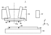
1 is a diagram illustrating a configuration of an imprint apparatus according to one aspect of the present invention.
FIG. 2 is a diagram illustrating a configuration of a correction mechanism of the imprint apparatus shown in FIG. 1.
3A and 3B are views for explaining a mold side mark and a substrate side mark.
4A to 4E illustrate deviations that occur between the shape and position of the pattern region of the mold and the shape and position of the shot region on the substrate.
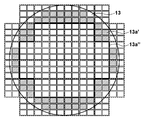
5 illustrates a partial shot region on a substrate.
FIG. 6 is a flowchart for explaining an operation of the imprint apparatus shown in FIG. 1. FIG.
7 shows an arrangement of a plurality of shot regions on a substrate.
Preferred embodiments of the present invention will be described below with reference to the accompanying drawings. Note that like reference numerals denote like elements throughout the drawings, and repetitive description thereof is omitted.
1 is a diagram illustrating a configuration of an
The
The
The
The
The substrate holder 14 is a holding mechanism for holding the
The
The correction mechanism (deformation unit) 16 deforms the
The
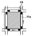
3A and 3B, a
3A shows mold-
FIG. 3B shows substrate-
When the imprint process is performed, that is, when the
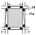
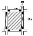
4A to 4E show a deviation (hereinafter, referred to as “
4A shows a state in which the shift between the
4B shows a state in which the deviation between the
4C shows a state in which the shift between the
4D shows a state where the deviation between the
4E shows a state in which the deviation between the
As shown in FIGS. 4B to 4E, when the shift between the
In the
As described above, all of the substrate side marks 19a to 19h to be formed in one shot region are not formed in the
Therefore, in the present embodiment, among the plurality of shot regions on the
Hereinafter, with reference to FIG. 6, the operation (imprint method using the imprint apparatus 1) of the
In step S602, the board | substrate 13 (refer FIG. 7) is carried in in the
In step S604, one
In step S606, an imprint process is performed on the
In step S608, it is determined whether or not all the
In step S610, one
In step S612, based on the result (detection result from the
In step S614, an imprint process is performed on the
In addition to the shape and position of the second shot region calculated in step S612, the method of using the detection result of the substrate-side mark formed in the
Further, according to the number of substrate-side marks (detectable by the scope 15) formed in the
In addition to the shape and position of the second shot region calculated in step S612, both the shape and the position can be corrected using the detection result of the substrate-side mark formed in the
In step S616, it is determined whether all the
In step S618, the pattern of the
As described above, in this embodiment, after the imprint process is performed on the
In this embodiment, the
In the present embodiment, the shape and position of the
In this embodiment, the first shot region where all of the substrate side marks to be formed in one shot region are formed is described as a shot region near the center of the substrate, and a part of the substrate side marks to be formed in one shot region is A second shot region not formed was described as a shot region near the periphery of the substrate.
However, the first shot area and the second shot area are not limited to the shot area. For example, in the shot region near the center of the substrate, a part of the substrate side mark to be formed in one shot region may be damaged by an external material. In this case, part of the substrate side mark cannot be detected in this shot area. Therefore, even if the specific shot region is a shot region near the center of the substrate, the specific shot in which a part of the substrate-side mark to be formed in one shot region is not formed may be assumed as the second shot region. By correcting the shape and position of the second shot region near the center of the substrate using the method described above, the imprint process can be performed without lowering the overlapping accuracy.
Also in this case, if an imprint process is performed (started) from the shot area near the center of the substrate, the shot area (shot area in which part of the substrate-side mark cannot be detected) assumed as the second shot area is an initial step. Can be generated from In this case, the imprint process can be performed while correcting the mold based on the information (shape and position of the shot region) of another substrate on which the imprint process has already been completed.
As described above, the
While the invention has been described with reference to exemplary embodiments, it will be understood that the invention is not limited to the disclosed exemplary embodiments. The scope of the following claims is to be accorded the broadest interpretation so as to encompass all such modifications and equivalent structures and functions.
Claims (14)
A detector configured to detect a mark formed in each of the plurality of shot regions on the substrate;
A deforming unit configured to deform the pattern region,
A controller configured to control the imprint process,
The plurality of shot regions may include a first shot region in which all of the marks to be formed in one shot region are formed, and a second shot region in which a part of the marks to be formed in one shot region is not formed.
When the controller performs the imprint process on the second shot region, the controller calculates the shape of the second shot region from the result obtained by detecting the mark formed in the first shot region with the detector, and calculates the calculated second second region. The imprint apparatus which controls the deformation amount of the said pattern area by the said deformation unit using the shape of a shot area.
The controller controls the deformation unit so that the difference between the calculated shape of the second shot region and the shape of the pattern region obtained from the result obtained by detecting the mark formed in the mold with the detector is reduced. Imprint device.
The controller is formed in the first shot region and the position of a mark formed in the mold detected by the detector when the mold and the imprint material are brought into contact with each other when the imprint process is performed on the first shot region. An imprint apparatus that controls the amount of deformation of the pattern region by the deformation unit so that the difference between the positions of the marks is reduced.
And the controller performs the imprint process on the second shot region after performing the imprint process on the first shot region.
The imprinter calculates the shape of the second shot region by statistically processing a result obtained by detecting the mark formed in the first shot region with the detector when performing the imprint process on the second shot region. Device.
The controller, when performing the imprint process on the second shot region, calculates the shape of the second shot region from the result obtained by detecting the mark formed in the first shot region adjacent to the second shot region with the detector. Imprint apparatus.
The controller, when performing the imprint process on the second shot region, results obtained by detecting a mark formed in the first shot region with the detector and a result obtained by detecting a mark formed in the second shot region with the detector. The imprint apparatus which calculates the shape of the said 2nd shot area | region from the.
The controller controls the amount of deformation of the pattern region by the deformation unit so that when the imprint process is performed on the second shot region, the shape of the pattern region is calculated so that the second shot region matches the shape. Imprint device.
The first shot region is an area where the entire pattern of the mold can be transferred,
And the second shot area is an area in which the entire pattern of the mold cannot be transferred.
A plurality of chip regions are formed in the pattern region,
All of the plurality of chip regions are transferred to the first shot region,
And at least one of the plurality of chip regions is transferred to the second shot region.
The controller calculates the position of the second shot region from the result obtained by detecting the mark formed in the first shot region with the detector when the imprint process is performed on the second shot region,
The controller is configured such that when the mold and the imprint material are brought into contact with each other, the calculated position of the second shot region matches the position of the pattern region obtained from the result obtained by detecting the mark formed in the mold with the detector. And positioning the mold and the substrate.
When the controller performs the imprint process on the first shot region, when the mold and the imprint material are brought into contact with each other, a position of a mark formed in the mold detected by the detector is formed in the first shot region. And position the mold and the substrate to coincide with the position of the mark.
The plurality of shot regions may include a first shot region in which all of the marks to be formed in one shot region are formed, and a second shot region in which a part of the marks to be formed in one shot region is not formed.
The imprint method,
When performing the imprint process on the second shot region, the shape of the second shot region is calculated from the result obtained by detecting the mark formed in the first shot region with the detector, and the calculated shape of the second shot region is obtained. And controlling the amount of deformation of the pattern region by using a method.
Processing the substrate on which the pattern is formed.
Applications Claiming Priority (4)
| Application Number | Priority Date | Filing Date | Title |
|---|---|---|---|
| JP2011262659 | 2011-11-30 | ||
| JPJP-P-2011-262659 | 2011-11-30 | ||
| JPJP-P-2012-233299 | 2012-10-22 | ||
| JP2012233299A JP6159072B2 (en) | 2011-11-30 | 2012-10-22 | Imprint apparatus, imprint method, and article manufacturing method |
Related Child Applications (1)
| Application Number | Title | Priority Date | Filing Date |
|---|---|---|---|
| KR1020150160733A Division KR101676195B1 (en) | 2011-11-30 | 2015-11-16 | Imprint apparatus, imprint method, and article manufacturing method |
Publications (1)
| Publication Number | Publication Date |
|---|---|
| KR20130061065A true KR20130061065A (en) | 2013-06-10 |
Family
ID=48466102
Family Applications (2)
| Application Number | Title | Priority Date | Filing Date |
|---|---|---|---|
| KR1020120132753A KR20130061065A (en) | 2011-11-30 | 2012-11-22 | Imprint apparatus, imprint method, and article manufacturing method |
| KR1020150160733A KR101676195B1 (en) | 2011-11-30 | 2015-11-16 | Imprint apparatus, imprint method, and article manufacturing method |
Family Applications After (1)
| Application Number | Title | Priority Date | Filing Date |
|---|---|---|---|
| KR1020150160733A KR101676195B1 (en) | 2011-11-30 | 2015-11-16 | Imprint apparatus, imprint method, and article manufacturing method |
Country Status (4)
| Country | Link |
|---|---|
| US (1) | US9915868B2 (en) |
| JP (1) | JP6159072B2 (en) |
| KR (2) | KR20130061065A (en) |
| CN (2) | CN103135340B (en) |
Cited By (3)
| Publication number | Priority date | Publication date | Assignee | Title |
|---|---|---|---|---|
| KR20160033038A (en) * | 2014-09-17 | 2016-03-25 | 캐논 가부시끼가이샤 | Imprint method, imprint apparatus, and method of manufacturing article |
| KR20190063404A (en) * | 2017-11-29 | 2019-06-07 | 캐논 가부시끼가이샤 | Imprint apparatus, imprint method and method of manufacturing article |
| US12078927B2 (en) | 2020-01-20 | 2024-09-03 | Canon Kabushiki Kaisha | Imprint method, imprint apparatus, and article manufacturing method |
Families Citing this family (13)
| Publication number | Priority date | Publication date | Assignee | Title |
|---|---|---|---|---|
| JP6159072B2 (en) * | 2011-11-30 | 2017-07-05 | キヤノン株式会社 | Imprint apparatus, imprint method, and article manufacturing method |
| JP6271875B2 (en) * | 2013-06-18 | 2018-01-31 | キヤノン株式会社 | Imprint apparatus, imprint method, and article manufacturing method |
| JP5960198B2 (en) * | 2013-07-02 | 2016-08-02 | キヤノン株式会社 | Pattern forming method, lithographic apparatus, lithographic system, and article manufacturing method |
| JP6360287B2 (en) * | 2013-08-13 | 2018-07-18 | キヤノン株式会社 | Lithographic apparatus, alignment method, and article manufacturing method |
| JP2015170815A (en) * | 2014-03-10 | 2015-09-28 | キヤノン株式会社 | Imprint device, alignment method, and manufacturing method for article |
| KR102311479B1 (en) * | 2014-04-01 | 2021-10-13 | 다이니폰 인사츠 가부시키가이샤 | Imprinting mold and imprinting method |
| US10331027B2 (en) * | 2014-09-12 | 2019-06-25 | Canon Kabushiki Kaisha | Imprint apparatus, imprint system, and method of manufacturing article |
| JP6497954B2 (en) | 2015-02-04 | 2019-04-10 | キヤノン株式会社 | Imprint method, imprint apparatus, and article manufacturing method |
| JP6700794B2 (en) * | 2015-04-03 | 2020-05-27 | キヤノン株式会社 | Imprint material discharge device |
| JP6207671B1 (en) * | 2016-06-01 | 2017-10-04 | キヤノン株式会社 | Pattern forming apparatus, substrate arranging method, and article manufacturing method |
| JP6921501B2 (en) * | 2016-10-26 | 2021-08-18 | キヤノン株式会社 | Imprinting method, imprinting equipment, and manufacturing method of goods |
| JP6940944B2 (en) * | 2016-12-06 | 2021-09-29 | キヤノン株式会社 | Imprint device and article manufacturing method |
| JP7022615B2 (en) * | 2018-02-26 | 2022-02-18 | キヤノン株式会社 | Imprint method, imprint device, mold manufacturing method, and article manufacturing method |
Family Cites Families (19)
| Publication number | Priority date | Publication date | Assignee | Title |
|---|---|---|---|---|
| US4780617A (en) | 1984-08-09 | 1988-10-25 | Nippon Kogaku K.K. | Method for successive alignment of chip patterns on a substrate |
| JPS6144429A (en) | 1984-08-09 | 1986-03-04 | Nippon Kogaku Kk <Nikon> | Alignment method |
| JPH0722102B2 (en) * | 1985-09-03 | 1995-03-08 | 株式会社ニコン | Exposure method |
| JPH09306811A (en) * | 1996-05-15 | 1997-11-28 | Nikon Corp | Method for exposure |
| US6258611B1 (en) | 1999-10-21 | 2001-07-10 | Vlsi Technology, Inc. | Method for determining translation portion of misalignment error in a stepper |
| JP4905617B2 (en) * | 2001-05-28 | 2012-03-28 | 株式会社ニコン | Exposure method and device manufacturing method |
| JP2005167030A (en) * | 2003-12-03 | 2005-06-23 | Sony Corp | Mask and exposure method |
| JP2006165371A (en) | 2004-12-09 | 2006-06-22 | Canon Inc | Transfer apparatus and device manufacturing method |
| JP4185941B2 (en) | 2006-04-04 | 2008-11-26 | キヤノン株式会社 | Nanoimprint method and nanoimprint apparatus |
| JP4958614B2 (en) | 2006-04-18 | 2012-06-20 | キヤノン株式会社 | Pattern transfer apparatus, imprint apparatus, pattern transfer method, and alignment apparatus |
| JP4795300B2 (en) | 2006-04-18 | 2011-10-19 | キヤノン株式会社 | Alignment method, imprint method, alignment apparatus, imprint apparatus, and position measurement method |
| JP5061525B2 (en) | 2006-08-04 | 2012-10-31 | 株式会社日立製作所 | Imprint method and imprint apparatus |
| JP2010080714A (en) * | 2008-09-26 | 2010-04-08 | Canon Inc | Stamping device, and method of manufacturing article |
| US8432548B2 (en) | 2008-11-04 | 2013-04-30 | Molecular Imprints, Inc. | Alignment for edge field nano-imprinting |
| JP5662741B2 (en) | 2009-09-30 | 2015-02-04 | キヤノン株式会社 | Imprint apparatus and article manufacturing method |
| JP5800456B2 (en) | 2009-12-16 | 2015-10-28 | キヤノン株式会社 | Detector, imprint apparatus, and article manufacturing method |
| JP5809409B2 (en) | 2009-12-17 | 2015-11-10 | キヤノン株式会社 | Imprint apparatus and pattern transfer method |
| JP5451450B2 (en) | 2010-02-24 | 2014-03-26 | キヤノン株式会社 | Imprint apparatus, template thereof, and article manufacturing method |
| JP6159072B2 (en) * | 2011-11-30 | 2017-07-05 | キヤノン株式会社 | Imprint apparatus, imprint method, and article manufacturing method |
-
2012
- 2012-10-22 JP JP2012233299A patent/JP6159072B2/en active Active
- 2012-11-02 US US13/667,325 patent/US9915868B2/en active Active
- 2012-11-22 KR KR1020120132753A patent/KR20130061065A/en active Search and Examination
- 2012-11-27 CN CN201210490618.1A patent/CN103135340B/en active Active
- 2012-11-27 CN CN201510167326.8A patent/CN104765249B/en active Active
-
2015
- 2015-11-16 KR KR1020150160733A patent/KR101676195B1/en active IP Right Grant
Cited By (4)
| Publication number | Priority date | Publication date | Assignee | Title |
|---|---|---|---|---|
| KR20160033038A (en) * | 2014-09-17 | 2016-03-25 | 캐논 가부시끼가이샤 | Imprint method, imprint apparatus, and method of manufacturing article |
| US10216103B2 (en) | 2014-09-17 | 2019-02-26 | Canon Kabushiki Kaisha | Imprint method, imprint apparatus, and method of manufacturing article |
| KR20190063404A (en) * | 2017-11-29 | 2019-06-07 | 캐논 가부시끼가이샤 | Imprint apparatus, imprint method and method of manufacturing article |
| US12078927B2 (en) | 2020-01-20 | 2024-09-03 | Canon Kabushiki Kaisha | Imprint method, imprint apparatus, and article manufacturing method |
Also Published As
| Publication number | Publication date |
|---|---|
| JP2013138175A (en) | 2013-07-11 |
| CN104765249A (en) | 2015-07-08 |
| CN103135340A (en) | 2013-06-05 |
| US20130134616A1 (en) | 2013-05-30 |
| JP6159072B2 (en) | 2017-07-05 |
| KR20150135175A (en) | 2015-12-02 |
| CN103135340B (en) | 2016-04-27 |
| CN104765249B (en) | 2019-09-03 |
| KR101676195B1 (en) | 2016-11-29 |
| US9915868B2 (en) | 2018-03-13 |
Similar Documents
| Publication | Publication Date | Title |
|---|---|---|
| KR101676195B1 (en) | Imprint apparatus, imprint method, and article manufacturing method | |
| JP5960198B2 (en) | Pattern forming method, lithographic apparatus, lithographic system, and article manufacturing method | |
| KR102032095B1 (en) | Method of curing uncured material and method of manufacturing article | |
| JP6120678B2 (en) | Imprint method, imprint apparatus and device manufacturing method | |
| JP6552329B2 (en) | Imprint apparatus, imprint system, and article manufacturing method | |
| KR101511411B1 (en) | Imprint apparatus, and method of manufacturing article | |
| US9971256B2 (en) | Imprint apparatus, imprint method, and method of manufacturing article | |
| CN105425538B (en) | Imprint apparatus, imprint system, and method of manufacturing article | |
| US20160349634A1 (en) | Mold, method and apparatus of imprinting, and method for producing product | |
| US10372033B2 (en) | Imprint apparatus, and method of manufacturing article | |
| JP2013219333A (en) | Imprint method, imprint device, and method for manufacturing article using the same | |
| JP6012209B2 (en) | Imprint apparatus and article manufacturing method | |
| JP2013219331A (en) | Imprint method, imprint device, and method for manufacturing article using the same | |
| US20160207248A1 (en) | Imprint apparatus, imprinting method, and method of manufacturing articles | |
| JP6381721B2 (en) | Imprint method, imprint apparatus and device manufacturing method | |
| JP7451141B2 (en) | Imprint device, imprint method, and article manufacturing method | |
| JP6792669B2 (en) | Pattern formation method, lithography equipment, lithography system and article manufacturing method | |
| KR20220027034A (en) | Imprint apparatus and method of manufacturing article | |
| KR20210117193A (en) | Imprint apparatus and article manufacturing method | |
| JP7421278B2 (en) | Imprint device and article manufacturing method | |
| JP2018018944A (en) | Imprint method and manufacturing method of article | |
| JP2016021443A (en) | Imprint device and article manufacturing method |
Legal Events
| Date | Code | Title | Description |
|---|---|---|---|
| A201 | Request for examination | ||
| AMND | Amendment | ||
| E902 | Notification of reason for refusal | ||
| AMND | Amendment | ||
| E601 | Decision to refuse application | ||
| A107 | Divisional application of patent | ||
| AMND | Amendment |