KR20130000409A - 실리콘 산화막의 형성 방법, 및 플라즈마 산화 처리 장치 - Google Patents
실리콘 산화막의 형성 방법, 및 플라즈마 산화 처리 장치 Download PDFInfo
- Publication number
- KR20130000409A KR20130000409A KR1020127026718A KR20127026718A KR20130000409A KR 20130000409 A KR20130000409 A KR 20130000409A KR 1020127026718 A KR1020127026718 A KR 1020127026718A KR 20127026718 A KR20127026718 A KR 20127026718A KR 20130000409 A KR20130000409 A KR 20130000409A
- Authority
- KR
- South Korea
- Prior art keywords
- gas
- plasma
- processing
- oxide film
- ozone
- Prior art date
- Legal status (The legal status is an assumption and is not a legal conclusion. Google has not performed a legal analysis and makes no representation as to the accuracy of the status listed.)
- Ceased
Links
Images


Classifications
-
- H—ELECTRICITY
- H10—SEMICONDUCTOR DEVICES; ELECTRIC SOLID-STATE DEVICES NOT OTHERWISE PROVIDED FOR
- H10P—GENERIC PROCESSES OR APPARATUS FOR THE MANUFACTURE OR TREATMENT OF DEVICES COVERED BY CLASS H10
- H10P14/00—Formation of materials, e.g. in the shape of layers or pillars
- H10P14/60—Formation of materials, e.g. in the shape of layers or pillars of insulating materials
- H10P14/69—Inorganic materials
- H10P14/692—Inorganic materials composed of oxides, glassy oxides or oxide-based glasses
- H10P14/6921—Inorganic materials composed of oxides, glassy oxides or oxide-based glasses containing silicon
- H10P14/69215—Inorganic materials composed of oxides, glassy oxides or oxide-based glasses containing silicon the material being a silicon oxide, e.g. SiO2
-
- H—ELECTRICITY
- H01—ELECTRIC ELEMENTS
- H01J—ELECTRIC DISCHARGE TUBES OR DISCHARGE LAMPS
- H01J37/00—Discharge tubes with provision for introducing objects or material to be exposed to the discharge, e.g. for the purpose of examination or processing thereof
- H01J37/32—Gas-filled discharge tubes
- H01J37/32009—Arrangements for generation of plasma specially adapted for examination or treatment of objects, e.g. plasma sources
- H01J37/32082—Radio frequency generated discharge
- H01J37/321—Radio frequency generated discharge the radio frequency energy being inductively coupled to the plasma
-
- H—ELECTRICITY
- H01—ELECTRIC ELEMENTS
- H01J—ELECTRIC DISCHARGE TUBES OR DISCHARGE LAMPS
- H01J37/00—Discharge tubes with provision for introducing objects or material to be exposed to the discharge, e.g. for the purpose of examination or processing thereof
- H01J37/32—Gas-filled discharge tubes
- H01J37/32009—Arrangements for generation of plasma specially adapted for examination or treatment of objects, e.g. plasma sources
- H01J37/32192—Microwave generated discharge
-
- H—ELECTRICITY
- H01—ELECTRIC ELEMENTS
- H01J—ELECTRIC DISCHARGE TUBES OR DISCHARGE LAMPS
- H01J37/00—Discharge tubes with provision for introducing objects or material to be exposed to the discharge, e.g. for the purpose of examination or processing thereof
- H01J37/32—Gas-filled discharge tubes
- H01J37/32431—Constructional details of the reactor
- H01J37/3244—Gas supply means
-
- H—ELECTRICITY
- H10—SEMICONDUCTOR DEVICES; ELECTRIC SOLID-STATE DEVICES NOT OTHERWISE PROVIDED FOR
- H10P—GENERIC PROCESSES OR APPARATUS FOR THE MANUFACTURE OR TREATMENT OF DEVICES COVERED BY CLASS H10
- H10P14/00—Formation of materials, e.g. in the shape of layers or pillars
- H10P14/60—Formation of materials, e.g. in the shape of layers or pillars of insulating materials
- H10P14/63—Formation of materials, e.g. in the shape of layers or pillars of insulating materials characterised by the formation processes
- H10P14/6302—Non-deposition formation processes
- H10P14/6304—Formation by oxidation, e.g. oxidation of the substrate
- H10P14/6306—Formation by oxidation, e.g. oxidation of the substrate of the semiconductor materials
- H10P14/6308—Formation by oxidation, e.g. oxidation of the substrate of the semiconductor materials of Group IV semiconductors
-
- H—ELECTRICITY
- H10—SEMICONDUCTOR DEVICES; ELECTRIC SOLID-STATE DEVICES NOT OTHERWISE PROVIDED FOR
- H10P—GENERIC PROCESSES OR APPARATUS FOR THE MANUFACTURE OR TREATMENT OF DEVICES COVERED BY CLASS H10
- H10P14/00—Formation of materials, e.g. in the shape of layers or pillars
- H10P14/60—Formation of materials, e.g. in the shape of layers or pillars of insulating materials
- H10P14/63—Formation of materials, e.g. in the shape of layers or pillars of insulating materials characterised by the formation processes
- H10P14/6326—Deposition processes
- H10P14/6328—Deposition from the gas or vapour phase
- H10P14/6334—Deposition from the gas or vapour phase using decomposition or reaction of gaseous or vapour phase compounds, i.e. chemical vapour deposition
- H10P14/6336—Deposition from the gas or vapour phase using decomposition or reaction of gaseous or vapour phase compounds, i.e. chemical vapour deposition in the presence of a plasma [PECVD]
Landscapes
- Physics & Mathematics (AREA)
- Engineering & Computer Science (AREA)
- Plasma & Fusion (AREA)
- Chemical & Material Sciences (AREA)
- Analytical Chemistry (AREA)
- Formation Of Insulating Films (AREA)
- Chemical Vapour Deposition (AREA)
Abstract
Description
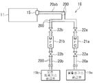
도 2는 가스 공급 장치의 구성 예를 나타내는 도면이다.
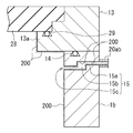
도 3은 처리 용기에 있어서의 가스 도입부의 확대 단면도이다.
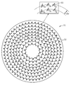
도 4는 평면 안테나의 구조를 도시한 도면이다.
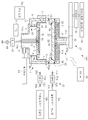
도 5는 제어부의 구성을 나타내는 설명도이다.
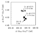
도 6은 실험 1에 있어서의 산화막의 XPS 스펙트럼으로부터 얻을 수 있는 실리콘 산화막의 결합 에너지와 실리콘의 결합 에너지의 차(세로축)와, 산소의 결합 에너지와 실리콘 산화막의 결합 에너지의 차(가로축)를 도시한 그래프이다.
도 7은 실험 2에 있어서의 실리콘 산화막의 막두께의 처리 압력 의존성을 나타내는 그래프다.
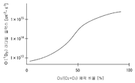
도 8a는 실험 3에 있어서의 전처리 가스 유량에 관한 오존 함유 가스 또는 산소 가스의 체적 유량 비율(가로축)과, 실리콘 산화막의 막두께(세로축)의 관계를 도시한 그래프이다.
도 8b는 O3/(O2+O3) 체적 비율과 O(1D2) 래디컬 플럭스(radical flux)의 관계를 설명하는 도면이다.
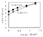
도 9는 실험 4에 있어서의 탑재대에 공급한 고주파 전력의 파워 밀도(가로축)와 실리콘 산화막의 웨이퍼 면내에 있어서의 균일성(세로축)과의 관계를 도시한 그래프이다.
도 10은 실험 4에 있어서의 고주파 파워 밀도(가로축)와 산화 막두께(세로축)의 관계를 도시한 그래프이다.
Claims (10)
- 플라즈마 처리 장치의 처리 용기 내에서, 피처리체의 표면에 노출한 실리콘에, O2와 O3의 체적의 합에 대한 O3의 체적 비율이 50 % 이상인 오존 함유 가스를 포함하는 처리 가스의 플라즈마를 작용시켜서 실리콘 산화막을 형성하는 공정을 포함하는,
실리콘 산화막의 형성 방법.
- 제 1 항에 있어서,
상기 처리 용기 내의 압력이 1.3Pa 이상 1333Pa 이하의 범위 내인 실리콘 산화막의 형성 방법.
- 제 1 항에 있어서,
상기 처리 용기 내에서 피처리체를 탑재하는 탑재대에 피처리체의 면적당 0.2W/cm2 이상 1.3W/cm2 이하의 범위 내의 출력으로 고주파 전력을 공급하면서 산화 처리를 실행하는 실리콘 산화막의 형성 방법.
- 제 1 항에 있어서,
처리 온도가, 피처리체의 온도로서 20℃ 이상 600℃ 이하의 범위 내인 것을 특징으로 하는 실리콘 산화막의 형성 방법.
- 제 1 항에 있어서,
상기 플라즈마가, 상기 처리 가스와 복수의 슬롯을 가지는 평면 안테나에 의해 상기 처리 용기 내에 도입되는 마이크로파에 의해 형성되는 마이크로파 여기 플라즈마인 것을 특징으로 하는 실리콘 산화막의 형성 방법.
- 제 5 항에 있어서,
상기 마이크로파의 파워 밀도가, 피처리체의 면적당 0.255W/cm2 이상 2.55W/cm2 이하의 범위 내인 것을 특징으로 하는 실리콘 산화막의 형성 방법.
- 플라즈마를 이용하여 피처리체를 처리하는 상부가 개구된 처리 용기와,
상기 처리 용기의 상기 개구부를 덮는 유전체 부재와,
상기 유전체 부재의 외측에 마련되고, 상기 처리 용기 내에 전자파를 도입하기 위한 안테나와,
상기 처리 용기 내에 오존 함유 가스를 포함하는 처리 가스를 도입하는 가스 도입부와,
상기 처리 용기 내를 배기 수단에 의해 감압 배기하는 배기구와,
상기 처리 용기 내에서 피처리체를 탑재하는 탑재대와,
상기 안테나에 의해 상기 처리 용기 내에 전자파를 도입함과 아울러, 상기 처리 용기 내에 O2와 O3의 체적의 합에 대한 O3의 체적 비율이 50 % 이상인 오존 함유 가스를 포함하는 처리 가스를 공급하고, 상기 처리 가스의 플라즈마를 생성시켜, 해당 플라즈마를 피처리체의 표면에 노출한 실리콘에 작용시켜서 실리콘 산화막을 형성하도록 제어하는 제어부
를 구비한 플라즈마 산화 처리 장치.
- 제 7 항에 있어서,
일단이 상기 가스 도입부에 접속되고, 타단이 오존 함유 가스 공급원에 접속되어, 내부에 부동태화 처리가 실시되어서 상기 오존 함유 가스를 상기 처리 용기 내에 공급하는 가스 공급 배관을 더 구비하고 있는 플라즈마 산화 처리 장치.
- 제 8 항에 있어서,
상기 가스 도입부는, 상기 처리 용기 내의 처리 공간에 가스를 분출하는 가스 구멍을 포함하는 가스 유로를 가지고 있고, 상기 가스 유로의 일부분 혹은 전체와 상기 가스 구멍의 주위의 처리 용기의 내벽면에, 부동태화 처리가 실시되어 있는 플라즈마 산화 처리 장치.
- 제 7 항에 있어서,
상기 탑재대에 피처리체의 면적당 0.2W/cm2 이상 1.3W/cm2 이하의 고주파 전력을 공급하는 고주파 전원을 더 구비하고 있는 플라즈마 산화 처리 장치.
Applications Claiming Priority (3)
| Application Number | Priority Date | Filing Date | Title |
|---|---|---|---|
| JP2010064080A JP2011199003A (ja) | 2010-03-19 | 2010-03-19 | シリコン酸化膜の形成方法、及びプラズマ処理装置 |
| JPJP-P-2010-064080 | 2010-03-19 | ||
| PCT/JP2011/055482 WO2011114961A1 (ja) | 2010-03-19 | 2011-03-09 | シリコン酸化膜の形成方法、及びプラズマ酸化処理装置 |
Publications (1)
| Publication Number | Publication Date |
|---|---|
| KR20130000409A true KR20130000409A (ko) | 2013-01-02 |
Family
ID=44649059
Family Applications (1)
| Application Number | Title | Priority Date | Filing Date |
|---|---|---|---|
| KR1020127026718A Ceased KR20130000409A (ko) | 2010-03-19 | 2011-03-09 | 실리콘 산화막의 형성 방법, 및 플라즈마 산화 처리 장치 |
Country Status (6)
| Country | Link |
|---|---|
| US (1) | US20130012033A1 (ko) |
| JP (1) | JP2011199003A (ko) |
| KR (1) | KR20130000409A (ko) |
| CN (1) | CN102714158A (ko) |
| TW (1) | TW201203365A (ko) |
| WO (1) | WO2011114961A1 (ko) |
Families Citing this family (14)
| Publication number | Priority date | Publication date | Assignee | Title |
|---|---|---|---|---|
| CN102427097B (zh) * | 2011-11-23 | 2014-05-07 | 中国科学院物理研究所 | 一种硅的氧化钝化方法及钝化装置 |
| JP5618098B2 (ja) * | 2012-04-23 | 2014-11-05 | 信越半導体株式会社 | C−v特性測定方法 |
| CN103695837B (zh) * | 2013-11-29 | 2015-09-30 | 莱芜钢铁集团有限公司 | 一种建筑钢筋表面防锈方法 |
| TWI524388B (zh) | 2013-12-27 | 2016-03-01 | 日立國際電氣股份有限公司 | A substrate processing apparatus, a manufacturing method of a semiconductor device, and a recording medium |
| US9583337B2 (en) | 2014-03-26 | 2017-02-28 | Ultratech, Inc. | Oxygen radical enhanced atomic-layer deposition using ozone plasma |
| JP6242283B2 (ja) * | 2014-04-30 | 2017-12-06 | 東京エレクトロン株式会社 | 成膜方法 |
| US20160277244A1 (en) * | 2015-03-18 | 2016-09-22 | ThePlatform, LLC. | Methods And Systems For Content Presentation Optimization |
| US9466504B1 (en) * | 2015-03-31 | 2016-10-11 | Micron Technology, Inc. | Methods of fabricating features associated with semiconductor substrates |
| CN108463930B (zh) * | 2016-01-08 | 2020-05-12 | 索尼公司 | 半导体发光器件、显示单元和电子设备 |
| JP7296855B2 (ja) * | 2019-11-07 | 2023-06-23 | 東京エレクトロン株式会社 | プラズマ処理装置及びプラズマ処理方法 |
| US12288672B2 (en) * | 2020-01-15 | 2025-04-29 | Applied Materials, Inc. | Methods and apparatus for carbon compound film deposition |
| US11512387B2 (en) * | 2020-04-13 | 2022-11-29 | Applied Materials, Inc. | Methods and apparatus for passivating a target |
| CN114649180B (zh) * | 2020-12-21 | 2025-04-08 | 中微半导体设备(上海)股份有限公司 | 等离子体处理装置零部件的处理方法、零部件及处理装置 |
| JP7743738B2 (ja) | 2021-09-14 | 2025-09-25 | 富士電機株式会社 | 半導体装置の製造方法 |
Family Cites Families (8)
| Publication number | Priority date | Publication date | Assignee | Title |
|---|---|---|---|---|
| JPH07118522B2 (ja) * | 1990-10-24 | 1995-12-18 | インターナショナル・ビジネス・マシーンズ・コーポレイション | 基板表面を酸化処理するための方法及び半導体の構造 |
| JPH08293494A (ja) * | 1995-04-24 | 1996-11-05 | Canon Inc | 半導体装置 |
| JPH11145131A (ja) * | 1997-03-18 | 1999-05-28 | Toshiba Corp | 半導体装置の製造方法及び半導体製造装置、及び半導体装置 |
| DE69940114D1 (de) * | 1999-08-17 | 2009-01-29 | Applied Materials Inc | Oberflächenbehandlung von kohlenstoffdotierten SiO2-Filmen zur Erhöhung der Stabilität während der O2-Veraschung |
| JP3615160B2 (ja) * | 2001-07-03 | 2005-01-26 | 株式会社半導体プロセス研究所 | 絶縁膜の形成方法及び液晶パネルの製造方法 |
| US7465674B2 (en) * | 2005-05-31 | 2008-12-16 | Semiconductor Energy Laboratory Co., Ltd. | Manufacturing method of semiconductor device |
| US7943531B2 (en) * | 2007-10-22 | 2011-05-17 | Applied Materials, Inc. | Methods for forming a silicon oxide layer over a substrate |
| JP5475261B2 (ja) * | 2008-03-31 | 2014-04-16 | 東京エレクトロン株式会社 | プラズマ処理装置 |
-
2010
- 2010-03-19 JP JP2010064080A patent/JP2011199003A/ja active Pending
-
2011
- 2011-03-09 CN CN2011800070263A patent/CN102714158A/zh active Pending
- 2011-03-09 WO PCT/JP2011/055482 patent/WO2011114961A1/ja not_active Ceased
- 2011-03-09 KR KR1020127026718A patent/KR20130000409A/ko not_active Ceased
- 2011-03-09 US US13/636,030 patent/US20130012033A1/en not_active Abandoned
- 2011-03-18 TW TW100109364A patent/TW201203365A/zh unknown
Also Published As
| Publication number | Publication date |
|---|---|
| US20130012033A1 (en) | 2013-01-10 |
| CN102714158A (zh) | 2012-10-03 |
| JP2011199003A (ja) | 2011-10-06 |
| WO2011114961A1 (ja) | 2011-09-22 |
| TW201203365A (en) | 2012-01-16 |
Similar Documents
| Publication | Publication Date | Title |
|---|---|---|
| KR20130000409A (ko) | 실리콘 산화막의 형성 방법, 및 플라즈마 산화 처리 장치 | |
| US10017853B2 (en) | Processing method of silicon nitride film and forming method of silicon nitride film | |
| KR100896552B1 (ko) | 플라즈마 에칭방법 | |
| JP5138261B2 (ja) | シリコン酸化膜の形成方法、プラズマ処理装置および記憶媒体 | |
| KR20120069755A (ko) | 선택적 플라즈마 질화 처리방법 및 플라즈마 질화 처리장치 | |
| JP5390379B2 (ja) | プラズマ窒化処理におけるチャンバ内の前処理方法、プラズマ処理方法、および記憶媒体 | |
| TW201207943A (en) | Plasma nitridization method | |
| JP5231232B2 (ja) | プラズマ酸化処理方法、プラズマ処理装置、及び、記憶媒体 | |
| KR101432415B1 (ko) | 플라즈마 질화 처리 방법 및 플라즈마 질화 처리 장치 | |
| JP4979575B2 (ja) | 基板の窒化処理方法および絶縁膜の形成方法 | |
| JP5271702B2 (ja) | シリコン酸化膜の形成方法およびシリコン酸化膜の形成装置 | |
| KR101255905B1 (ko) | 실리콘 산화막의 형성 방법 및 장치 | |
| CN102737946A (zh) | 等离子体处理方法 | |
| TW201130398A (en) | Microwave plasma processing device and microwave plasma processing method | |
| KR20230096113A (ko) | 기판 처리 방법 및 기판 처리 장치 | |
| TW200834731A (en) | Plasma oxidizing method | |
| WO2004070815A1 (ja) | プラズマ酸化処理方法及び半導体基板 |
Legal Events
| Date | Code | Title | Description |
|---|---|---|---|
| A201 | Request for examination | ||
| PA0105 | International application |
St.27 status event code: A-0-1-A10-A15-nap-PA0105 |
|
| PA0201 | Request for examination |
St.27 status event code: A-1-2-D10-D11-exm-PA0201 |
|
| E13-X000 | Pre-grant limitation requested |
St.27 status event code: A-2-3-E10-E13-lim-X000 |
|
| P11-X000 | Amendment of application requested |
St.27 status event code: A-2-2-P10-P11-nap-X000 |
|
| P13-X000 | Application amended |
St.27 status event code: A-2-2-P10-P13-nap-X000 |
|
| PG1501 | Laying open of application |
St.27 status event code: A-1-1-Q10-Q12-nap-PG1501 |
|
| E902 | Notification of reason for refusal | ||
| PE0902 | Notice of grounds for rejection |
St.27 status event code: A-1-2-D10-D21-exm-PE0902 |
|
| E601 | Decision to refuse application | ||
| PE0601 | Decision on rejection of patent |
St.27 status event code: N-2-6-B10-B15-exm-PE0601 |
|
| P22-X000 | Classification modified |
St.27 status event code: A-2-2-P10-P22-nap-X000 |
|
| P22-X000 | Classification modified |
St.27 status event code: A-2-2-P10-P22-nap-X000 |