KR20130000409A - Silicon oxide film forming method, and plasma oxidation apparatus - Google Patents
Silicon oxide film forming method, and plasma oxidation apparatus Download PDFInfo
- Publication number
- KR20130000409A KR20130000409A KR1020127026718A KR20127026718A KR20130000409A KR 20130000409 A KR20130000409 A KR 20130000409A KR 1020127026718 A KR1020127026718 A KR 1020127026718A KR 20127026718 A KR20127026718 A KR 20127026718A KR 20130000409 A KR20130000409 A KR 20130000409A
- Authority
- KR
- South Korea
- Prior art keywords
- gas
- plasma
- processing
- oxide film
- ozone
- Prior art date
- Legal status (The legal status is an assumption and is not a legal conclusion. Google has not performed a legal analysis and makes no representation as to the accuracy of the status listed.)
- Ceased
Links
Images


Classifications
-
- H—ELECTRICITY
- H10—SEMICONDUCTOR DEVICES; ELECTRIC SOLID-STATE DEVICES NOT OTHERWISE PROVIDED FOR
- H10P—GENERIC PROCESSES OR APPARATUS FOR THE MANUFACTURE OR TREATMENT OF DEVICES COVERED BY CLASS H10
- H10P14/00—Formation of materials, e.g. in the shape of layers or pillars
- H10P14/60—Formation of materials, e.g. in the shape of layers or pillars of insulating materials
- H10P14/69—Inorganic materials
- H10P14/692—Inorganic materials composed of oxides, glassy oxides or oxide-based glasses
- H10P14/6921—Inorganic materials composed of oxides, glassy oxides or oxide-based glasses containing silicon
- H10P14/69215—Inorganic materials composed of oxides, glassy oxides or oxide-based glasses containing silicon the material being a silicon oxide, e.g. SiO2
-
- H—ELECTRICITY
- H01—ELECTRIC ELEMENTS
- H01J—ELECTRIC DISCHARGE TUBES OR DISCHARGE LAMPS
- H01J37/00—Discharge tubes with provision for introducing objects or material to be exposed to the discharge, e.g. for the purpose of examination or processing thereof
- H01J37/32—Gas-filled discharge tubes
- H01J37/32009—Arrangements for generation of plasma specially adapted for examination or treatment of objects, e.g. plasma sources
- H01J37/32082—Radio frequency generated discharge
- H01J37/321—Radio frequency generated discharge the radio frequency energy being inductively coupled to the plasma
-
- H—ELECTRICITY
- H01—ELECTRIC ELEMENTS
- H01J—ELECTRIC DISCHARGE TUBES OR DISCHARGE LAMPS
- H01J37/00—Discharge tubes with provision for introducing objects or material to be exposed to the discharge, e.g. for the purpose of examination or processing thereof
- H01J37/32—Gas-filled discharge tubes
- H01J37/32009—Arrangements for generation of plasma specially adapted for examination or treatment of objects, e.g. plasma sources
- H01J37/32192—Microwave generated discharge
-
- H—ELECTRICITY
- H01—ELECTRIC ELEMENTS
- H01J—ELECTRIC DISCHARGE TUBES OR DISCHARGE LAMPS
- H01J37/00—Discharge tubes with provision for introducing objects or material to be exposed to the discharge, e.g. for the purpose of examination or processing thereof
- H01J37/32—Gas-filled discharge tubes
- H01J37/32431—Constructional details of the reactor
- H01J37/3244—Gas supply means
-
- H—ELECTRICITY
- H10—SEMICONDUCTOR DEVICES; ELECTRIC SOLID-STATE DEVICES NOT OTHERWISE PROVIDED FOR
- H10P—GENERIC PROCESSES OR APPARATUS FOR THE MANUFACTURE OR TREATMENT OF DEVICES COVERED BY CLASS H10
- H10P14/00—Formation of materials, e.g. in the shape of layers or pillars
- H10P14/60—Formation of materials, e.g. in the shape of layers or pillars of insulating materials
- H10P14/63—Formation of materials, e.g. in the shape of layers or pillars of insulating materials characterised by the formation processes
- H10P14/6302—Non-deposition formation processes
- H10P14/6304—Formation by oxidation, e.g. oxidation of the substrate
- H10P14/6306—Formation by oxidation, e.g. oxidation of the substrate of the semiconductor materials
- H10P14/6308—Formation by oxidation, e.g. oxidation of the substrate of the semiconductor materials of Group IV semiconductors
-
- H—ELECTRICITY
- H10—SEMICONDUCTOR DEVICES; ELECTRIC SOLID-STATE DEVICES NOT OTHERWISE PROVIDED FOR
- H10P—GENERIC PROCESSES OR APPARATUS FOR THE MANUFACTURE OR TREATMENT OF DEVICES COVERED BY CLASS H10
- H10P14/00—Formation of materials, e.g. in the shape of layers or pillars
- H10P14/60—Formation of materials, e.g. in the shape of layers or pillars of insulating materials
- H10P14/63—Formation of materials, e.g. in the shape of layers or pillars of insulating materials characterised by the formation processes
- H10P14/6326—Deposition processes
- H10P14/6328—Deposition from the gas or vapour phase
- H10P14/6334—Deposition from the gas or vapour phase using decomposition or reaction of gaseous or vapour phase compounds, i.e. chemical vapour deposition
- H10P14/6336—Deposition from the gas or vapour phase using decomposition or reaction of gaseous or vapour phase compounds, i.e. chemical vapour deposition in the presence of a plasma [PECVD]
Landscapes
- Physics & Mathematics (AREA)
- Engineering & Computer Science (AREA)
- Plasma & Fusion (AREA)
- Chemical & Material Sciences (AREA)
- Analytical Chemistry (AREA)
- Formation Of Insulating Films (AREA)
- Chemical Vapour Deposition (AREA)
Abstract
처리 용기(1) 내를 배기 장치(24)에 의해 감압 배기하면서, 가스 공급 장치(18)의 불활성 가스 공급원(19a) 및 오존 함유 가스 공급원(19b)으로부터, 불활성 가스 및 O2와 O3의 합계의 체적에 대한 O3의 체적 비율이 50% 이상인 오존 함유 가스를 소정의 유량으로 가스 도입부(5)를 거쳐서 처리 용기(1) 내에 도입한다. 마이크로파 발생 장치(39)에서 발생된 소정 주파수, 예를 들어 2.45GHz의 마이크로파를, 평면 안테나(31)로부터 투과판(28)을 경유하여 처리 용기(1)로 방사하고, 불활성 가스 및 오존 함유 가스를 플라즈마한다. 이 마이크로파 여기 플라즈마에 의해 웨이퍼(W) 표면에 실리콘 산화막을 형성한다. 플라즈마 산화 처리 동안에, 탑재대(2)에 고주파 전원(44)으로부터 소정의 주파수 및 파워의 고주파 전력을 공급하여도 좋다.From the inert gas supply source 19a and the ozone-containing gas supply source 19b of the gas supply device 18, the inert gas and the O 2 and O 3 are discharged while evacuating the inside of the processing container 1 by the exhaust device 24. the volume ratio of O 3 the ozone containing gas is 50% or more of the total volume of the predetermined flow rate through the gas introduction section (5) is introduced into the treatment container (1). A microwave of a predetermined frequency generated by the microwave generator 39, for example, 2.45 GHz, is radiated from the planar antenna 31 to the processing container 1 via the transmission plate 28, and the inert gas and the ozone-containing gas are emitted. Plasma. A silicon oxide film is formed on the surface of the wafer W by this microwave excited plasma. During the plasma oxidation process, the high frequency power of a predetermined frequency and power may be supplied to the mounting table 2 from the high frequency power supply 44.

Description
본 발명은, 예를 들면, 각종의 반도체 장치의 제조 과정에 적용 가능한 실리콘 산화막의 형성 방법 및 플라즈마 처리 장치에 관한 것이다.The present invention relates to, for example, a method for forming a silicon oxide film and a plasma processing apparatus that can be applied to manufacturing processes of various semiconductor devices.
각종 반도체 장치의 제조 과정에서는, 실리콘 기판을 산화 처리해서 실리콘 산화막을 형성하는 것이 실행된다. 실리콘 표면에 실리콘 산화막을 형성하는 방법으로서는, 산화로나 RTP(Rapid Thermal Process) 장치를 이용하는 열산화 처리와, 플라즈마 처리 장치를 이용하는 플라즈마 산화 처리가 알려져 있다. In the manufacturing process of various semiconductor devices, the silicon substrate is oxidized to form a silicon oxide film. As a method for forming a silicon oxide film on a silicon surface, thermal oxidation treatment using an oxidation furnace or a rapid thermal process (RTP) apparatus and a plasma oxidation treatment using a plasma processing apparatus are known.
예를 들면, 열산화 처리의 하나인 산화로에 의한 습식 산화 처리에서는, 800도를 넘는 온도로 실리콘 기판을 가열하고, WVG(Water Vapor Generator) 장치에서 생성한 수증기를 이용하여 산화 분위기에 노출함으로써, 실리콘 표면을 산화해서 실리콘 산화막을 형성한다. 열산화 처리는, 양질의 실리콘 산화막을 형성할 수 있는 방법이다. 그러나, 열산화 처리는, 800도를 넘는 고온에 의한 처리가 필요하기 때문에, 열소모비용(thermal budget)이 증대하고, 열 응력에 의해 실리콘 기판에 왜곡 등이 생기는 문제가 있다. For example, in the wet oxidation treatment by an oxidation furnace, which is one of thermal oxidation treatments, a silicon substrate is heated to a temperature exceeding 800 degrees and exposed to an oxidizing atmosphere by using water vapor generated by a water vapor generator (WVG) device. The silicon surface is oxidized to form a silicon oxide film. The thermal oxidation treatment is a method capable of forming a high quality silicon oxide film. However, since thermal oxidation treatment requires processing at a high temperature of more than 800 degrees, a thermal budget increases, and there is a problem that distortion or the like occurs in the silicon substrate due to thermal stress.
한편, 플라즈마 산화 처리는, 일반적으로 산소 가스를 이용하여 산화 처리가 실행된다. 예를 들면, 국제 공개 WO2004/008519호에서는, 아르곤 가스와 산소 가스를 포함하고, 산소의 유량 비율이 약 1%인 처리 가스를 이용하고, 133.3 Pa의 처리 용기 내 압력에서 형성된 마이크로파 여기 플라즈마를 실리콘 표면에 작용시켜서 플라즈마 산화 처리를 실행하는 방법이 제안되어 있다. 이 WO2004/008519호에 개시된 방법에서는, 처리 온도가 400도 전후와 비교적 저온에서 플라즈마 산화 처리가 실행되기 때문에, 열산화 처리에 있어서의 열 처리량의 증대나 기판의 왜곡 등의 문제를 피할 수 있다. On the other hand, the plasma oxidation treatment is generally carried out using an oxygen gas. For example, in International Publication No. WO 2004/008519, a microwave-excited plasma formed at a pressure in a processing vessel of 133.3 Pa by using a processing gas containing argon gas and oxygen gas and having a flow rate ratio of oxygen of about 1% is silicon. A method of performing plasma oxidation treatment by acting on the surface has been proposed. In the method disclosed in WO2004 / 008519, the plasma oxidation treatment is performed at a treatment temperature of about 400 degrees and at a relatively low temperature, so that problems such as an increase in the heat treatment amount and distortion of the substrate in the thermal oxidation treatment can be avoided.
또한, 산소 가스의 대체 가스로서, 오존 가스를 이용하여 플라즈마 산화 처리를 실행하는 기술도 제안되어 있다. 예를 들면, 일본 공개 특허 공보 제 10500386 호에서는, 마이크로파 방전 구멍 안에서 약 1 torr까지의 압력으로 오존을 분해함으로써 형성된 오존 분해 생성물 흐름에 약 300도 이하의 온도에서 규소 함유 고체를 반응시켜, 이산화규소의 박막을 형성하는 방법이 제안되어 있다. Moreover, the technique of performing a plasma oxidation process using ozone gas as a substitute gas of oxygen gas is also proposed. For example, Japanese Laid-Open Patent Publication No. 10500386 discloses a silicon dioxide solid by reacting a silicon-containing solid at a temperature of about 300 degrees or less to an ozone decomposition product stream formed by decomposing ozone at a pressure of about 1 torr in a microwave discharge hole. A method of forming a thin film of has been proposed.
또한, ECR(전자 사이클론 공명) 플라즈마를 이용한 실리콘 웨이퍼의 산화 처리에 있어서, 1.3 Pa의 처리 압력에서, 산소 가스를 이용할 경우보다도 오존 가스를 이용하는 경우가, 산화 레이트가 높은 것으로 보고되어 있다 [마츠무라 유키테루, T.IEE Japan, Vol. 111A, NO. 12, 1991]. 또한, 이 문헌에서는, ECR플라즈마를 이용하고, 극저압의 1Pa 이하의 처리 압력에서 형성된 실리콘 산화막의 계면 준위 밀도는, 산소 가스를 이용할 경우와 오존 가스를 이용할 경우에서 거의 동등한 것도 개시되어 있다.In addition, in the oxidation treatment of silicon wafers using ECR (electron cyclone resonance) plasma, it is reported that the oxidation rate is higher when ozone gas is used than when oxygen gas is used at a processing pressure of 1.3 Pa [Matsumura]. Yukiteru, T.IEE Japan, Vol. 111A, NO. 12, 1991]. This document also discloses that the interface state density of a silicon oxide film formed by using an ERC plasma and formed at a processing pressure of 1 Pa or less at an extremely low pressure is almost equal when oxygen gas is used and ozone gas is used.
일반적으로, 플라즈마 산화 처리에 의해 형성된 실리콘 산화막은, 열산화 처리에 의해 형성된 실리콘 산화막에 비해, 플라즈마(이온 등)에 의한 대미지가 들어가므로 막질의 관점에서 떨어진다고 생각되고 있다. 그것이, 열산화 처리가 현재에서도 널리 이용되고 있는 이유로 되어 있다. 그러나, 플라즈마 산화 처리에 의해, 열 산화막과 동등한 양질인 막질의 실리콘 산화막을 형성할 수 있으면, 고온에서의 열산화 처리에 따른 문제도 회피할 수 있다. 따라서, 플라즈마 산화 처리에 의해, 막질이 개선된 실리콘 산화막을 형성할 수 있는 방법이 요구되고 있다.In general, the silicon oxide film formed by the plasma oxidation treatment is considered to be inferior from the viewpoint of the film quality since the damage caused by plasma (ions, etc.) enters the silicon oxide film formed by the thermal oxidation treatment. That is the reason why the thermal oxidation treatment is widely used now. However, if the plasma oxide treatment can form a silicon oxide film having a high quality film equivalent to that of the thermal oxide film, the problem caused by the thermal oxidation at high temperature can be avoided. Therefore, there is a need for a method capable of forming a silicon oxide film having improved film quality by plasma oxidation treatment.
본 발명은, 상기 사정을 감안하여 이루어진 것이며, 열 산화막과 동등 이상의 막질을 가지는 실리콘 산화막을 형성할 수 있는 플라즈마 산화 처리 방법을 제공하는 것을 목적으로 한다.
This invention is made | formed in view of the said situation, and an object of this invention is to provide the plasma oxidation processing method which can form the silicon oxide film which has a film quality equivalent to or more than a thermal oxide film.
본 발명의 실리콘 산화막의 형성 방법은, 플라즈마 처리 장치의 처리 용기 내에서, 피처리체의 표면에 노출한 실리콘에, O2과 O3의 합계의 체적에 대한 O3의 체적 비율이 50 % 이상인 오존 함유 가스를 포함하는 처리 가스의 플라즈마를 작용시켜서 실리콘 산화막을 형성하는 공정을 포함하고 있다. Method of forming a silicon oxide film of the present invention, in a processing container of a plasma processing apparatus, at least a silicon exposed on the surface of the object piece, O 2 and O 3 volume ratio of the volume of the total of the O 3 is 50% Ozone A process of forming a silicon oxide film by acting the plasma of the process gas containing a containing gas is included.
본 발명의 실리콘 산화막의 형성 방법은, 상기 처리 용기 내의 압력이 1.3Pa 이상 1333Pa 이하의 범위 내이여도 좋다. The pressure in the said processing container may be in the range of 1.3 Pa or more and 1333 Pa or less in the formation method of the silicon oxide film of this invention.
또한, 본 발명의 실리콘 산화막의 형성 방법은, 상기 처리 용기 내에서 피처리체를 탑재하는 탑재대에 고주파 전력을 공급하면서 산화 처리를 실행하는 것이라도 좋다. 이런 경우, 상기 고주파 전력은, 피처리체의 면적당 0.2W/cm2 이상 1.3W/cm2 이하의 범위 내의 출력으로 공급되는 것이 바람직하다. The silicon oxide film forming method of the present invention may be subjected to an oxidation process while supplying high frequency power to a mounting table on which a target object is to be mounted in the processing container. In this case, the high frequency electric power is preferably supplied to the output in the processing target area 0.2W / cm 2 more than 1.3W / cm 2 within the following range.
또한, 본 발명의 실리콘 산화막의 형성 방법은, 처리 온도가, 피처리체의 온도로서 20도 이상 600도 이하의 범위 내이여도 좋다. Moreover, in the formation method of the silicon oxide film of this invention, process temperature may be in the range of 20 degreeC or more and 600 degrees or less as the temperature of a to-be-processed object.
또한, 본 발명의 실리콘 산화막의 형성 방법은, 상기 플라즈마가, 상기 처리 가스와, 복수의 슬롯을 가지는 평면 안테나에 의해 상기 처리 용기 내에 도입되는 마이크로파에 의해 형성되는 마이크로파 여기 플라즈마이여도 좋다. 이런 경우, 상기 마이크로파의 파워 밀도가, 피처리체의 면적당 0.255W/cm2 이상 2.55W/cm2 이하의 범위 내인 것이 바람직하다. In addition, the method for forming the silicon oxide film of the present invention may be a microwave-excited plasma in which the plasma is formed by microwaves introduced into the processing container by the processing gas and a planar antenna having a plurality of slots. In this case, the power density of the microwave, it is preferred that the subject to be treated per 0.255W / cm 2 more than 2.55W / cm 2 or less within a range of.
본 발명의 플라즈마 산화 처리 장치는, 플라즈마를 이용하여 피처리체를 처리하는 상부가 개구된 처리 용기와, 상기 처리 용기의 상기 개구부를 덮는 유전체 부재와, 상기 유전체 부재의 외측에 마련되고, 상기 처리 용기 내에 전자파를 도입하기 위한 안테나와, 상기 처리 용기 내에 오존 함유 가스를 포함하는 처리 가스를 도입하는 가스 도입부와, 상기 처리 용기 내를 배기 수단에 의해 감압 배기하는 배기구와, 상기 처리 용기 내에서 피처리체를 탑재하는 탑재대와, 상기 안테나에 의해 상기 처리 용기 내에 전자파를 도입함과 아울러, 상기 처리 용기 내에 O2과 O3의 합계의 체적에 대한 O3의 체적 비율이 50 % 이상인 오존 함유 가스를 포함하는 처리 가스를 공급하고, 그 처리 가스의 플라즈마를 생성시켜, 해당 플라즈마를 피처리체의 표면에 노출한 실리콘에 작용시켜서 실리콘 산화막을 형성하도록 제어하는 제어부를 구비하는 것이다. The plasma oxidation processing apparatus of the present invention is provided with a processing vessel having an upper portion for processing a target object using plasma, a dielectric member covering the opening of the processing vessel, and an outer side of the dielectric member, An antenna for introducing electromagnetic waves into the inside, a gas introducing unit for introducing a processing gas containing an ozone-containing gas into the processing container, an exhaust port for evacuating the inside of the processing container by an exhausting means, and an object to be processed in the processing container And an ozone-containing gas having a volume ratio of O 3 to a volume of the total of O 2 and O 3 in the processing container while introducing electromagnetic waves into the processing container by the mounting table and the antenna. Supply a processing gas to be produced, generate a plasma of the processing gas, and expose the plasma to the surface of the object to be processed. By acting to the silicon to a control unit for controlling so as to form a silicon oxide film.
본 발명의 플라즈마 산화 처리 장치는, 또한, 일단이 상기 가스 도입부에 접속되고, 타단이 오존 함유 가스 공급원에 접속되어, 내부에 부동태화 처리가 실시되어서 상기 오존 함유 가스를 상기 처리실내에 공급하는 가스 공급 배관을 구비하고 있어도 좋다. 이런 경우, 상기 가스 도입부는, 상기 처리 용기 내의 처리 공간에 가스를 분출하는 가스 구멍을 포함하는 가스 유로를 가지고 있고, 상기 가스 유로의 일부분 혹은 전체와, 상기 가스 구멍의 주위의 처리 용기의 내벽면에, 부동태화 처리가 실시되어 있어도 좋다. In the plasma oxidation treatment apparatus of the present invention, a gas for supplying the ozone-containing gas to the processing chamber is further provided with one end connected to the gas inlet, the other end connected to an ozone-containing gas supply source, and undergoing a passivation treatment therein. Supply piping may be provided. In this case, the gas introduction portion has a gas flow path including a gas hole for ejecting gas into the processing space in the processing container, wherein a part or the entirety of the gas flow path and an inner wall surface of the processing container around the gas hole are provided. The passivation process may be performed.
또한, 본 발명의 플라즈마 산화 처리 장치에 있어서, 상기 탑재대에 피처리체의 면적당 0.2W/cm2 이상 1.3W/cm2 이하의 고주파 전력을 공급하는 고주파 전원을 더 구비하고 있어도 좋다.
Further, in a plasma oxidation treatment apparatus of the present invention, it may further comprises a high-frequency power to the mounting table supplying the area of the object piece 0.2W / cm 2 more than 1.3W / cm 2 or less in the high-frequency power.
본 발명의 실리콘 산화막의 형성 방법에 따르면, O2와 O3의 합계의 체적에 대한 O3의 체적 비율이 50 % 이상인 오존 함유 가스를 포함하는 처리 가스의 플라즈마를 작용시켜서 실리콘 산화막을 형성하는 것에 의해, 열산화막과 동등 이상의 양질의 막질을 가지는 실리콘 산화막을 형성할 수 있다.
According to the method for forming a silicon oxide film of the present invention, the silicon oxide film is formed by applying a plasma of a processing gas containing an ozone-containing gas having a volume ratio of O 3 to 50% or more to the total volume of O 2 and O 3 . This makes it possible to form a silicon oxide film having a film quality that is equal to or higher than that of the thermal oxide film.
도 1은 본 발명의 실리콘 산화막의 형성 방법의 실시에 적합한 플라즈마 처리 장치의 일예를 나타내는 개략 단면도이다.
도 2는 가스 공급 장치의 구성 예를 나타내는 도면이다.
도 3은 처리 용기에 있어서의 가스 도입부의 확대 단면도이다.
도 4는 평면 안테나의 구조를 도시한 도면이다.
도 5는 제어부의 구성을 나타내는 설명도이다.
도 6은 실험 1에 있어서의 산화막의 XPS 스펙트럼으로부터 얻을 수 있는 실리콘 산화막의 결합 에너지와 실리콘의 결합 에너지의 차(세로축)와, 산소의 결합 에너지와 실리콘 산화막의 결합 에너지의 차(가로축)를 도시한 그래프이다.
도 7은 실험 2에 있어서의 실리콘 산화막의 막두께의 처리 압력 의존성을 나타내는 그래프다.
도 8a는 실험 3에 있어서의 전처리 가스 유량에 관한 오존 함유 가스 또는 산소 가스의 체적 유량 비율(가로축)과, 실리콘 산화막의 막두께(세로축)의 관계를 도시한 그래프이다.
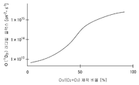
도 8b는 O3/(O2+O3) 체적 비율과 O(1D2) 래디컬 플럭스(radical flux)의 관계를 설명하는 도면이다.
도 9는 실험 4에 있어서의 탑재대에 공급한 고주파 전력의 파워 밀도(가로축)와 실리콘 산화막의 웨이퍼 면내에 있어서의 균일성(세로축)과의 관계를 도시한 그래프이다.
도 10은 실험 4에 있어서의 고주파 파워 밀도(가로축)와 산화 막두께(세로축)의 관계를 도시한 그래프이다.1 is a schematic cross-sectional view showing an example of a plasma processing apparatus suitable for carrying out the method for forming a silicon oxide film of the present invention.
2 is a diagram illustrating a configuration example of a gas supply device.
3 is an enlarged cross-sectional view of a gas introduction unit in a processing container.
4 is a diagram illustrating a structure of a planar antenna.
5 is an explanatory diagram showing a configuration of a control unit.
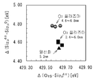
Fig. 6 shows the difference (vertical axis) between the bond energy of the silicon oxide film and the bond energy of silicon obtained from the XPS spectrum of the oxide film in
7 is a graph showing the processing pressure dependence of the film thickness of the silicon oxide film in
8A is a graph showing the relationship between the volume flow rate ratio (horizontal axis) of ozone-containing gas or oxygen gas and the film thickness (vertical axis) of the silicon oxide film with respect to the pretreatment gas flow rate in
8B is a view for explaining the relationship between the O 3 / (O 2 + O 3 ) volume ratio and the O ( 1 D 2 ) radical flux.
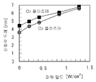
9 is a graph showing the relationship between the power density (horizontal axis) of the high frequency power supplied to the mounting table in
FIG. 10 is a graph showing the relationship between the high frequency power density (horizontal axis) and the oxide film thickness (vertical axis) in
이하, 본 발명의 실시예에 대해서 도면을 참조해서 상세히 설명한다. 도 1은, 본 발명의 일실시예에 따른 실리콘 산화막의 형성 방법에 이용 가능한 플라즈마 처리 장치(100)의 개략 구성을 모식적으로 나타내는 단면도이다. EMBODIMENT OF THE INVENTION Hereinafter, the Example of this invention is described in detail with reference to drawings. 1 is a cross-sectional view schematically showing a schematic configuration of a
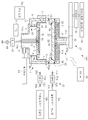
플라즈마 처리 장치(100)는, 복수의 슬롯 형상의 구멍을 가지는 평면 안테나, 특히 RLSA(Radial Line Slot Antenna ; 래디얼 라인 슬롯 안테나)로 처리 용기 내에 마이크로파를 도입해서 처리 용기 내에서 플라즈마를 발생시킴으로써, 고밀도 또한 저전자 온도의 마이크로파 여기 플라즈마를 발생시킬 수 있는 RLSA 마이크로파 플라즈마 처리 장치로서 구성되어 있다. 플라즈마 처리 장치(100)에서는, 예를 들면, 1× 10¹⁰∼5× 10¹²/cm3의 플라즈마 밀도이고, 또한 0.7∼2eV의 저전자 온도를 가지는 플라즈마에 의한 처리가 가능하다. 따라서, 플라즈마 처리 장치(100)는, 각종 반도체 장치의 제조 과정에 있어서, 실리콘 산화막(예를 들면 SiO2막)을 형성할 목적으로 적절히 이용할 수 있다. The
플라즈마 처리 장치(100)는, 주요 구성으로서, 기밀하게 구성된 처리 용기(1)와, 가스 공급 장치(18)에 접속되어서 처리 용기(1) 내에 가스를 도입하는 가스 도입부(15)와, 처리 용기(1) 내를 감압 배기하기 위한 배기 장치(24)에 접속된 배기구(1lb)와, 처리 용기(1)의 상부에 마련되고, 처리 용기(1) 내에 마이크로파를 도입하는 마이크로파 도입 장치(27)와, 플라즈마 처리 장치(100)의 각 구성부를 제어하는 제어부(50)를 구비하고 있다. 또, 가스 공급 장치(18)는, 플라즈마 처리 장치(100)의 일부분으로서도 좋고, 일부분이 아니라, 외부의 기구로서 플라즈마 처리 장치(100)에 접속하는 구성으로도 좋다. The
처리 용기(1)는, 접지된 대략 원통 형상의 용기에 의해 형성되어 있다. 처리 용기(1)는, 알루미늄 등의 재질로 이루어지는 저벽(1a)과 측벽(1b)을 가지고 있다. 또, 처리 용기(1)는 각통 형상의 용기에 의해 형성해도 좋다. The
처리 용기(1)의 내부에는, 피처리체인 실리콘 기판(웨이퍼(W))을 수평으로 지지하기 위한 탑재대(2)가 마련되어 있다. 탑재대(2)는, 열전도성의 높은 재질, 예를 들면, AlN 등의 세라믹스에 의해 구성되어 있다. 이 탑재대(2)는, 배기실(11)의 바닥부 중앙으로부터 상방으로 연장하는 원통 형상의 지지 부재(3)에 의해 지지되어 있다. 지지 부재(3)는, 예를 들면, AlN 등의 세라믹스에 의해 구성되어 있다. Inside the
또한, 탑재대(2)에는, 그 외연부를 커버하고, 웨이퍼(W)를 가이드하기 위한 커버링(4)이 마련되어 있다. 이 커버링(4)은, 링 형상으로 형성되어 있어도 좋고, 탑재대(2)의 전면에 형성되어 있어도 좋지만, 탑재대(2)의 전면을 커버하고 있는 것이 바람직하다. 커버링(4)에 의해, 웨이퍼(W)에의 불순물의 혼입 방지를 도모할 수 있다. 커버링(4)은, 예를 들면, 석영, 단결정 실리콘, 폴리 실리콘, 비정질 실리콘, SiN 등의 재질로 구성되고, 이들 중에서도 석영이 가장 바람직하다. 또한, 커버링(4)을 구성하는 상기 재질은, 알칼리 금속, 금속 등의 불순물의 함유량이 적은 고순도의 것이 바람직하다. In addition, the mounting table 2 is provided with a
또한, 탑재대(2)에는, 온도 조절 장치로서의 저항 가열형의 히터(5)가 매설되어 있다. 이 히터(5)는, 히터 전원(5a)으로부터 급전함으로써 탑재대(2)를 가열하고, 그 열로부터 피처리체인 웨이퍼(W)를 균일하게 가열한다. In the mounting table 2, a
또한, 탑재대(2)에는, 열전대(TC)(6)가 배치되어 있다. 이 열전대(6)에 의해 온도 계측을 행함으로써, 웨이퍼(W)의 가열 온도를, 예를 들면, 실온으로부터 900도까지의 범위에서 제어 가능해지고 있다. In addition, a thermocouple (TC) 6 is disposed on the mounting table 2. By performing temperature measurement by this
또한, 탑재대(2)에는, 웨이퍼(W)를 지지해서 승강시키기 위한 웨이퍼 지지 핀(도시하지 않음)이 마련되어 있다. 각 웨이퍼 지지 핀은, 탑재대(2)의 표면에 대하여 돌출 및 함몰 가능하게 마련되어 있다. In addition, the mounting table 2 is provided with a wafer support pin (not shown) for supporting and lifting the wafer W. As shown in FIG. Each wafer support pin is provided so that protrusion and depression may be made with respect to the surface of the mounting table 2.
처리 용기(1)의 내주에는, 석영으로 이루어지는 원통 형상의 라이너(7)가 마련되어 있다. 또한, 탑재대(2)의 외주측에는, 처리 용기(1) 내를 균일 배기하기 위해서, 다수의 배기 구멍(8a)을 가진 석영제의 배플 플레이트(8)가 링 형상으로 마련되어 있다. 이 배플 플레이트(8)는, 복수의 지주(9)에 의해 지지되어 있다. At the inner circumference of the
처리 용기(1)의 저벽(1a)의 대략 중앙부에는, 원형의 개구부(10)가 형성되어 있다. 저벽(1a)에는 이 개구부(10)와 연직 하방을 향해서 돌출하는 배기실(11)이 마련되어 있다. 이 배기실(11)에는, 배기구(11b)가 마련되고, 해당 배기구(11b)에 배기관(12)이 접속되어 있다. 배기실(11)은, 이 배기관(12)을 거쳐서 배기 수단으로서의 배기 장치(24)에 접속되어 있다. The
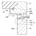
처리 용기(1)의 상부에는, 링 형상의 플레이트(13)가 접합되어 있다. 플레이트(13)의 내주는, 내측(처리 용기 내 공간)을 향해서 돌출하고, 링 형상의 지지부(13a)를 형성하고 있다. 이 플레이트(13)와 처리 용기(1)의 사이는, 시일 부재(14)를 거쳐서 기밀하게 시일되어 있다. A ring-shaped
가스 도입부(15)는, 처리 용기(1)의 측벽(1b)에 링 형상으로 마련되어 있다. 이 가스 도입부(15)는, 처리 가스를 공급하는 가스 공급 장치(18)에 접속되어 있다. 또, 가스 도입부(15)는 노즐 형상 또는 샤워 형상으로 마련해도 좋다. 가스 도입부(15)의 구조에 대해서는, 후술한다. The
또한, 처리 용기(1)의 측벽(1b)에는, 플라즈마 처리 장치(100)와, 이것에 인접하는 반송실(도시하지 않음)의 사이에서, 웨이퍼(W)의 반출입을 실행하기 위한 반입출구(16)와, 이 반입출구(16)를 개폐하는 게이트 밸브(17)가 마련되어 있다. In addition, the
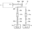
가스 공급 장치(18)는, 예를 들면, 불활성 가스 공급원(19a)과 오존 함유 가스 공급원(19b)을 가지고 있다. 또, 가스 공급 장치(18)는, 상기 이외의 도시하지 않는 가스 공급원으로서, 예를 들면, 처리 용기(1) 내 분위기를 치환할 때에 이용하는 퍼지 가스 공급원 등을 가지고 있어도 좋다. The
불활성 가스는, 안정한 플라즈마를 생성하기 위한 플라즈마 여기용 가스로서 사용된다. 불활성 가스로서는, 예를 들면, 희가스 등을 이용할 수 있다. 희가스로서는, 예를 들면 Ar 가스, Kr 가스, Xe 가스, He 가스 등을 이용할 수 있다. 이들 중에서도, 경제성에서 우수하고, 플라즈마를 안정되게 생성 가능해서 균일한 플라즈마 산화 처리를 실현할 수 있는 Ar 가스를 이용하는 것이 특히 바람직하다. An inert gas is used as a gas for plasma excitation for producing a stable plasma. As an inert gas, a rare gas etc. can be used, for example. As rare gas, Ar gas, Kr gas, Xe gas, He gas, etc. can be used, for example. Among these, it is especially preferable to use Ar gas which is excellent in economy and can generate plasma stably and can realize uniform plasma oxidation treatment.
오존 함유 가스는, 분해해서 플라즈마를 구성하는 산소 래디컬이나 산소 이온이 되고, 실리콘에 작용해서 실리콘을 산화하는 산소원의 가스이다. 또, 본 명세서에 있어서, 「오존 함유 가스」는, 특별히 제외하지 않는 한, O2과 O3를 포함하는 가스룰 의미한다. 오존 함유 가스로서는, 가스 중에 포함되는 O2과 O3의 합계에 대한 O3의 체적 비율이 50% 이상, 바람직하게는, 60% 이상 80% 이하의 범위 내인 고농도의 오존 함유 가스를 이용할 수 있다. 이렇게, 고농도의 오존(O3)을 포함하는 오존 함유 가스를 이용하는 것에 의해, 실리콘 산화막의 막질을 향상시킬 수 있다. The ozone-containing gas is oxygen radicals or oxygen ions that decompose to form plasma, and is an oxygen source gas that acts on silicon and oxidizes silicon. In the present specification, "ozone-containing gas" is meant gas rule comprising a, O 2 and O 3 is not specifically excluded. As the ozone-containing gas, the O 2 and O total volume ratio of O 3 for the third at least 50%, and preferably, the ozone containing gas, a high concentration within a range between 60% to 80% contained in the gas can be used . Thus, by using an ozone-containing gas containing high concentration of ozone (O 3 ), the film quality of the silicon oxide film can be improved.
도 2는 가스 공급 장치(18)에 있어서의 배관 구성을 확대해서 도시한 도면이며, 도 3은 처리 용기(1)에 있어서의 가스 도입부의 구성을 확대해서 도시한 도면이다. 불활성 가스는, 불활성 가스 공급원(19a)으로부터, 가스 공급 배관인 가스 라인(20a), 가스 라인(20ab)을 거쳐서 가스 도입부(15)에 도달하고, 가스 도입부(15)로부터 처리 용기(1) 내에 도입된다. 또한, 오존 함유 가스는, 오존 함유 가스 공급원(19b)으로부터, 가스 공급 배관인 가스 라인(20b), 가스 라인(20ab)을 통해 가스 도입부(15)에 도달하고, 가스 도입부(15)로부터 처리 용기(1) 내에 도입된다. 가스 라인(20a)과 가스 라인(20b)은, 도중에 합류해서 하나의 가스 라인(20ab)을 구성하고 있다. 각 가스 공급원에 접속하는 각각의 가스 라인(20a, 20b)에는, 각각 매스플로우 컨트롤러(21a, 2lb) 및 그 전후의 개폐 밸브(22a, 22b)가 마련되어 있다. 이러한 가스 공급 장치(18)의 구성에 의해, 공급되는 가스의 전환이나 유량 등의 제어를 할 수 있도록 되어 있다. FIG. 2 is an enlarged view of the piping configuration of the
오존 함유 가스 공급원(19b)은, 예를 들면, 고농도의 O3을 포함하는 오존 함유 가스를 저류하는 오존 함유 가스 봄베(bomb)이여도 좋고, 또는, 고농도의 O3을 포함하는 오존 함유 가스를 발생시키는 오조나이저(ozonizer)이여도 좋다. 또한, O2 가스 공급원과 O3 가스 공급원을 가지고, 따로따로 공급하도록 해도 좋다. 오존 함유 가스 공급원(19b)으로부터 가스 도입부(15)까지를 접속하는 가스 라인(20b, 20ab)의 내표면은, 고농도의 O3을 포함하는 오존 함유 가스를 통류(通流)시킬 때에, 오존의 자기 분해(실활(失活))와 이상 반응을 막기 위한 부동태화 처리가 실시되어 있다. 부동태화 처리는, 예를 들면, 스테인레스 등의 재질의 가스 라인(20b, 20ab)의 내벽면을, 고농도의 O3을 포함하는 오존 함유 가스로부터 노출함으로써 실행할 수 있다. 이에 따라, 스테인레스의 조성인 Fe 원소, Cr 원소가 산화되어, 금속 산화물의 부동태 피막(200)이, 가스 라인(20b, 20ab)의 내표면에 형성된다. 구체적으로는, 부동태화 처리는, 예를 들면, O2과 O3의 합계에 대한 O3의 체적 비율이 15∼50 체적%의 오존 함유 가스를, 예를 들면, 60도∼150도의 온도 범위에서, 금속 표면에 작용시키는 것에 의해 실행하는 것이 바람직하다. 이런 경우, 오존 함유 가스 중에 2 체적% 이하의 수분을 함유시킴으로써, 부동태 피막(200)의 형성을 빠르게 할 수 있다. Ozone-containing gas supply source (19b) is, for example, may be O high-concentration ozone-containing gas cylinder (bomb) for storing the ozone-containing gas containing O 3, or an ozone-containing gas containing a high concentration of O 3 It may be an ozonizer generated. In addition, the O 2 gas supply source and the O 3 gas supply source may be provided and supplied separately. The inner surfaces of the
또한, 본 실시예의 플라즈마 처리 장치(100)에서는, 고농도의 O3을 포함하는 오존 함유 가스를 처리 용기(1) 내에 도입하기 위해서, 처리 용기(1)에 형성된 가스 도입부(15)에도, 부동태화 처리가 실시되어 있다. 처리 용기(1)의 가스 도입부(15)는, 가스 라인(20ab)에 접속하는 가스 유로를 가지고 있고, 이들 가스 유로의 일부분 또는 전체에, 가스 라인(20b 및 20ab)과 마찬가지의 부동태화 처리가 이루어져, 부동태 피막(200)이 형성되어 있다. 보다 구체적으로는, 가스 도입부(15)는, 처리 용기(1)의 내부에 형성된 가스 도입로(15a)와, 이 가스 도입로(15a)에 연통하고, 처리 용기(1)의 벽 내에 거의 수평 방향으로 링 형상으로 마련된 공통 분배로(15b)와, 이 공통 분배로(15b)로부터 처리 용기(1)의 내부의 처리 공간까지를 연통시키는 복수의 가스 구멍(15c)을 가지고 있다. 각 가스 구멍(15c)은, 처리 용기(1) 내의 처리 공간에 접하는 개구부이며, 해당 처리 공간을 향해서 가스를 분출한다. 본 실시예에서는, 가스 도입로(15a), 공통 분배로(15b)의 내면에 부동태 피막(200)이 형성되어 있다. 또, 필요에 따라서, 가스 구멍(15c)의 부분에도 마찬가지로 부동태화 처리를 실시할 수 있다. In addition, in the
또한, 본 실시예의 플라즈마 처리 장치(100)에서는, 고농도의 O3을 포함하는 오존 함유 가스를 사용하기 때문에, 처리 용기(1)에 접하는 가스 구멍(15c)의 주위의 벽면에도 부동태화 처리가 실시되어 있다. 즉, 도 3에 도시하는 바와 같이, 가스 구멍(15c)이 마련된 처리 용기(1)의 측벽(1b)의 내벽면 및, 플레이트(13)의 지지부(13a)의 벽면에도, 부동태 피막(200)이 형성되어 있다. In addition, in the
이상과 같이, 가스 라인(20b, 20ab), 가스 도입로(15a), 공통 분배로(15b)의 내벽면, 또한, 처리 용기(1)의 가스 구멍(15c)의 주위의 벽면에도, 부동태화 처리를 실시해서 부동태 피막(200)을 마련함으로써, 종래의 플라즈마 처리 장치에서는 사용할 수 없었던 고농도의 오존 함유 가스를 사용하는 것, 및 고농도의 상태를 유지하면서 오존 함유 가스를 안정적으로 처리 용기(1) 내에 공급하는 것이 가능해지고, 고농도 오존 함유 가스를 이용한 플라즈마 처리가 가능하게 된다. As described above, the
배기 장치(24)는, 예를 들면, 터보 분자 펌프 등의 고속 진공 펌프를 구비하고 있다. 상기와 같이, 배기 장치(24)는, 배기관(12)을 거쳐서 처리 용기(1)의 배기실(11)에 접속되어 있다. 처리 용기(1) 내의 가스는, 배기실(11)의 공간(11a) 내에 균일하게 흐르고, 또한 배기 장치(24)를 작동시킴으로써, 공간(11a)으로부터 배기구(11b), 및 배기관(12)을 거쳐서 외부로 배기된다. 이에 따라, 처리 용기(1) 내를 소정의 진공도, 예를 들면, 0.133Pa까지 고속으로 감압하는 것이 가능해지고 있다. The
다음에, 마이크로파 도입 장치(27)의 구성에 대해서 설명한다. 마이크로파 도입 장치(27)는, 주요 구성으로서, 유전체 부재로서의 투과판(28), 안테나로서의 평면 안테나(31), 지파재(遲波材)(33), 커버 부재(34), 도파관(37), 매칭 회로(38) 및 마이크로파 발생 장치(39)를 구비하고 있다. Next, the structure of the
마이크로파를 투과시키는 투과판(28)은, 플레이트(13)에 있어서 내주측에 돌출한 지지부(13a) 위에 배치되어 있다. 투과판(28)은, 유전체, 예를 들면, 석영이나 Al2O3, AlN 등의 세라믹스 등의 부재로 구성되어 있다. 이 투과판(28)과 지지부(13a)의 사이는, O링 등의 시일 부재(29)를 거쳐서 기밀하게 시일되어 있다. 따라서, 처리 용기(1) 내는 기밀하게 유지된다. The permeation |
안테나로서의 평면 안테나(31)는, 투과판(28)의 상방(처리 용기(1)의 외측)에 있어서, 탑재대(2)와 대향하도록 마련되어 있다. 평면 안테나(31)는, 원판 형상을 이루고 있다. 또, 평면 안테나(31)의 형상은, 원판 형상으로 한정되지 않고, 예를 들면, 사각판 형상으로도 좋다. 이 평면 안테나(31)는, 플레이트(13)의 상단에 계지(係止)되어 있다. The
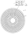
평면 안테나(31)는, 예를 들면, 표면이 금 또는 은 도금된 동판, 알루미늄판, 니켈판 및 그들의 합금 등의 도전성 부재로 구성되어 있다. 평면 안테나(31)는, 마이크로파를 방사하는 다수의 슬롯 형상의 마이크로파 방사 구멍(32)을 가지고 있다. 마이크로파 방사 구멍(32)은, 소정의 패턴으로 평면 안테나(31)를 관통해서 형성되어 있다. The
도 4는 도 1의 플라즈마 처리 장치(100)의 평면 안테나를 나타내는 평면도이다. 각각의 마이크로파 방사 구멍(32)은, 예를 들면, 도 4에 도시하는 바와 같이, 가늘고 긴 직사각형 형상(슬롯 형상)을 이루고 있다. 그리고, 전형적으로는 인접하는 마이크로파 방사 구멍(32)이 「T」자 형상으로 배치되어 있다. 또한, 이와 같이 소정의 형상(예를 들면 T자 형상)으로 조합해서 배치된 마이크로파 방사 구멍(32)은, 또한 전체로서 동심원 형상으로 배치되어 있다. 4 is a plan view illustrating the planar antenna of the
마이크로파 방사 구멍(32)의 길이나 배열 간격은, 마이크로파의 파장(λg)에 따라 결정된다. 예를 들면, 마이크로파 방사 구멍(32)의 간격은, λg/4, λg/2 또는 λg로 되도록 배치된다. 또, 도 4에 있어서는, 동심원 형상으로 형성된 인접하는 마이크로파 방사 구멍(32)끼리의 간격을 △r로 나타내고 있다. 또, 마이크로파 방사 구멍(32)의 형상은, 원형 형상, 원호 형상 등의 다른 형상이여도 좋다. 또한, 마이크로파 방사 구멍(32)의 배치 형태는 특별히 한정되지 않고, 동심원 형상 이외, 예를 들면, 나선 형상, 방사상 등으로도 배치할 수 있다. The length and arrangement interval of the microwave radiation holes 32 are determined depending on the wavelength λg of the microwaves. For example, the space | interval of the
평면 안테나(31)의 상면에는, 진공보다도 큰 유전율을 가지는 지파재(33)가 마련되어 있다. 이 지파재(33)는, 진공중에서는 마이크로파의 파장이 길어지기 때문에, 마이크로파의 파장을 짧게 해서 플라즈마를 조정하는 기능을 가지고 있다. 지파재의 재질로서는, 예를 들면 석영, 폴리 데트라플루오로에틸렌 수지, 폴리이미드 수지 등을 이용할 수 있다. On the upper surface of the
또, 평면 안테나(31)와 투과판(28)의 사이, 또한, 지파재(33)와 평면 안테나(31)의 사이는, 각각 접촉시켜도 이간시켜도 좋지만, 접촉시키는 것이 바람직하다. The
처리 용기(1)의 상부에는, 이들 평면 안테나(31) 및 지파재(33)를 덮도록, 커버 부재(34)가 마련되어 있다. 커버 부재(34)는, 예를 들면, 알루미늄이나 스테인리스강 등의 금속 재료에 의해 형성되어 있다. 커버 부재(34)와 평면 안테나(31)에 의해, 편평 도파로가 형성되어, 마이크로파를 처리 용기(1) 내에 균일하게 공급할 수 있도록 되어 있다. 플레이트(13)의 상단과 커버 부재(34)는, 시일 부재(35)에 의해 시일되어 있다. 또한, 커버 부재(34)의 내부에는, 냉각수 유로(34a)가 형성되어 있다. 이 냉각수 유로(34a)에 냉각수를 통류시킴으로써, 커버 부재(34), 지파재(33), 평면 안테나(31) 및 투과판(28)을 냉각할 수 있게 되어 있다. 또, 커버 부재(34)는 접지되어 있다. The
커버 부재(34)의 상벽(천장부)의 중앙에는, 개구부(36)가 형성되어 있고, 이 개구부(36)에는 도파관(37)이 접속되어 있다. 도파관(37)의 타단측에는, 매칭 회로(38)를 거쳐서 마이크로파를 발생하는 마이크로파 발생 장치(39)가 접속되어 있다. An
도파관(37)은, 상기 커버 부재(34)의 개구부(36)로부터 상방으로 연장하는 단면 원형 형상의 동축 도파관(37a)과, 이 동축 도파관(37a)의 상단부에 모드 변환기(40)를 거쳐서 접속된 수평 방향으로 연장하는 직사각형 도파관(37b)을 가지고 있다. 모드 변환기(40)는, 직사각형 도파관(37b) 내를 TE 모드로 전파하는 마이크로파를 TEM 모드로 변환하는 기능을 가지고 있다. The
동축 도파관(37a)의 중심에는 내측 도체(41)가 연재하고 있다. 이 내측 도체(41)는, 그 하단부에 있어서 평면 안테나(31)의 중심으로 접속 고정되어 있다. 이러한 구조에 의해, 마이크로파는, 동축 도파관(37a)의 내측 도체(41)를 통하여 평면 안테나(31)에 의해 형성되는 편평 도파로에 방사상으로 효율적으로 균일하게 전파된다. An
이상과 같은 구성의 마이크로파 도입 장치(27)에 의해, 마이크로파 발생 장치(39)에서 발생한 마이크로파가 도파관(37)을 통하여 평면 안테나(31)에 전파되고, 또한 마이크로파 방사 구멍(32)(슬롯)으로부터 투과판(28)을 거쳐서 처리 용기(1) 내에 도입되도록 되어 있다. 또, 마이크로파의 주파수로서는, 예를 들면, 2.45GHz가 바람직하게 이용되고, 이외에 8.35GHz, 1.98GHz 등을 이용할 수도 있다. By the
또한, 탑재대(2)의 표면측에는 전극(42)이 매설되어 있다. 이 전극(42)에 매칭 박스(M.B.)(43)를 거쳐서 바이어스 인가용의 고주파 전원(44)이 접속되어 있다. 전극(42)에 고주파 바이어스 전력을 공급함으로써, 웨이퍼(W)(피처리체)에 바이어스 전압을 인가할 수 있는 구성으로 되어 있다. 전극(42)의 재질로서는, 예를 들면, 몰리브덴, 텅스텐 등의 도전성 재료를 이용할 수 있다. 전극(42)은, 예를 들면, 그물망 형상, 격자 형상, 소용돌이 형상 등의 형상으로 형성되어 있다. Moreover, the
플라즈마 처리 장치(100)의 각 구성부는, 제어부(50)에 접속되어서 제어되는 구성으로 되어 있다. 제어부(50)는, 전형적으로는 컴퓨터이며, 예를 들면, 도 5에 나타낸 바와 같이, CPU를 구비한 프로세스 컨트롤러(51)와, 이 프로세스 컨트롤러(51)에 접속된 유저 인터페이스(52) 및 기억부(53)를 구비하고 있다. 프로세스 컨트롤러(51)는, 플라즈마 처리 장치(100)에 있어서, 예를 들면, 온도, 압력, 가스 유량, 마이크로파 출력, 바이어스 인가용의 고주파 출력 등의 프로세스 조건에 관계되는 각 구성부(예를 들면, 히터 전원(5a), 가스 공급 장치(18), 배기 장치(24), 마이크로파 발생 장치(39), 고주파 전원(44) 등)를 통괄해서 제어하는 제어 수단이다. Each component of the
유저 인터페이스(52)는, 공정 관리자가 플라즈마 처리 장치(100)를 관리하기 위해서 커맨드의 입력 조작 등을 실행하는 키보드나, 플라즈마 처리 장치(100)의 가동 상황을 가시화해서 표시하는 디스플레이 등을 가지고 있다. 또한, 기억부(53)에는, 플라즈마 처리 장치(100)에서 실행되는 각종 처리를 프로세스 컨트롤러(51)의 제어에서 실현하기 위한 제어 프로그램(소프트웨어)이나 처리 조건 데이터 등이 기록된 레시피 등이 보존되어 있다. The
그리고, 필요에 따라서, 유저 인터페이스(52)로부터의 지시 등으로 임의의 레시피를 기억부(53)로부터 호출해서 프로세스 컨트롤러(51)에 실행시킴으로써, 프로세스 컨트롤러(51)에 의해 제어되어서 플라즈마 처리 장치(100)의 처리 용기(1) 내에서 소망하는 처리가 실행된다. 또한, 상기 제어 프로그램이나 처리 조건 데이터 등의 레시피는, 컴퓨터 판독 가능한 기억 매체, 예를 들면, CD-ROM, 하드 디스크, 플렉시블디스크, 플래쉬 메모리, DVD, 블루레이 디스크 등에 저장된 상태의 것을 이용할 수 있다. 또한, 상기 레시피를 다른 장치로부터, 예를 들면, 전용 회선을 거쳐서 전송시켜서 이용하는 것도 가능하다. Then, if necessary, arbitrary recipes are called from the
이와 같이 구성된 플라즈마 처리 장치(100)에서는, 600도 이하, 예를 들면, 실온(20도 정도) 이상 600도 이하의 저온에서, 웨이퍼(W) 상에 형성된 기초막 등에의 대미지 없는 플라즈마 처리를 실행할 수 있다. 또한, 플라즈마 처리 장치(100)는, 플라즈마의 균일성에 우수하기 때문에, 대구경의 웨이퍼(W)(피처리체)에 대하여도 프로세스의 균일성을 실현할 수 있다. In the
다음에, RLSA 방식의 플라즈마 처리 장치(100)를 이용한 플라즈마 산화 처리에 대해서 설명한다. 우선, 게이트밸브(17)를 개방해서 반입출구(16)로부터 웨이퍼(W)를 처리 용기(1) 내에 반입하고, 탑재대(2) 상에 탑재한다. 웨이퍼(W)는, 탑재대(2)에 매설된 히터(5)에 의해, 소정의 온도까지 가열된다. Next, the plasma oxidation treatment using the RLSA
다음에, 처리 용기(1) 내를 배기 장치(24)의 진공 펌프에 의해 감압 배기하면서, 가스 공급 장치(18)의 불활성 가스 공급원(19a), 및 오존 함유 가스 공급원(19b)으로부터, 부동태화 처리된 가스 공급 배관(가스 라인(20b, 20ab))을 거쳐서 불활성 가스 및 고농도의 O3을 포함하는 오존 함유 가스를 소정의 유량으로 각각 가스 도입부(15)로부터 처리 용기(1) 내에 도입한다. 이렇게 하여, 처리 용기(1) 내를 소정의 압력으로 조절한다. Next, while evacuating the inside of the
다음에, 마이크로파 발생 장치(39)에서 발생시킨 소정 주파수, 예를 들면 2.45GHz의 마이크로파를, 매칭 회로(38)를 거쳐서 도파관(37)으로 유도한다. 도파관(37)에 유도된 마이크로파는, 직사각형 도파관(37b) 및 동축 도파관(37a)을 순차적으로 통과하고, 내측 도체(41)를 거쳐서 평면 안테나(31)에 공급된다. 즉, 마이크로파는, 직사각형 도파관(37b) 내에서는 TEM 모드로 전파하고, 이 TEM 모드의 마이크로파는 모드 변환기(40)에서 TEM 모드로 변환되어서, 동축 도파관(37a) 내를 평면 안테나(31)를 향해서 전파되어 간다. 그리고, 마이크로파는, 평면 안테나(31)에 관통 형성된 슬롯 형상의 마이크로파 방사 구멍(32)로부터 유전체 부재로서의 투과판(28)을 거쳐서 처리 용기(1) 내에 있어서의 웨이퍼(W)의 상방 공간에 방사된다. 이때의 마이크로파 출력은, 예를 들면, 200mm 직경 이상의 웨이퍼(W)를 처리할 경우에는, 파워 밀도로서 0.255∼2.55W/cm2의 범위 내에서 선택할 수 있다. Next, a microwave of a predetermined frequency generated by the
평면 안테나(31)로부터 투과판(28)을 거쳐서 처리 용기(1)에 방사된 마이크로파에 의해, 처리 용기(1) 내에 전자계가 형성되어, 불활성 가스 및 오존 함유 가스가 각각 플라즈마화한다. 이 마이크로파 여기 플라즈마는, 마이크로파가 평면 안테나(31)의 다수의 마이크로파 방사 구멍(32)로부터 방사함으로써, 거의 1× 10¹⁰∼5× 10¹²/cm3의 고밀도에서, 또한 웨이퍼(W) 근방에서는, 대략 1.2eV 이하의 저전자 온도 플라즈마가 된다. 이렇게 하여 형성되는 플라즈마는, 웨이퍼(W)에의 이온 등에 의한 플라즈마 대미지가 적다. 그 결과, 플라즈마 중의 활성종, 예를 들면, 래디컬이나 이온의 작용에 의해 웨이퍼(W) 표면에 형성된 실리콘(단결정 실리콘, 다결정 실리콘 또는 비정질 실리콘)에 대하여 플라즈마 산화 처리가 실행되고, 양질의 실리콘 산화막이 형성된다. The electromagnetic field is formed in the
또한, 플라즈마 산화 처리를 실행하고 있는 동안, 필요에 따라서 탑재대(2)에 고주파 전원(44)으로부터 소정의 주파수 및 파워의 고주파 전력을 공급할 수 있다. 이 고주파 전원(44)으로부터 공급되는 고주파 전력에 의해, 웨이퍼(W)에 고주파 바이어스 전압(고주파 바이어스)이 인가된다. 그 결과, 플라즈마의 낮은 전자 온도를 유지하면서, 플라즈마 산화 처리의 이방성이 촉진된다. 즉, 고주파 바이어스가 웨이퍼(W)에 인가됨으로써, 웨이퍼(W)의 근방에 전자계가 형성되고, 이것이 플라즈마 중의 이온을 웨이퍼(W)에 인입하도록 작용하기 때문에, 산화 레이트를 증대시키도록 작용한다. In addition, while performing the plasma oxidation process, high frequency power of predetermined frequency and power can be supplied to the mounting table 2 from the high
<플라즈마 산화 처리 조건> <Plasma oxidation treatment condition>
여기서, 플라즈마 처리 장치(100)에 있어서 실행되는 플라즈마 산화 처리의 바람직한 조건에 대해서 설명을 실행한다. 처리 가스로서는, 오존 함유 가스와 함께, 불활성 가스로서 Ar 가스를 사용하는 것이 바람직하다. 오존 함유 가스로서는, 오존 함유 가스 중에 포함되는 O2과 O3의 합계에 대한 O3의 체적 비율이 50 % 이상, 바람직하게는 60 % 이상 80 % 이하의 범위 내인 고농도의 오존 함유 가스를 이용한다. 고농도 오존을 포함하는 가스의 플라즈마에서는, O(1D2) 래디컬의 생성량이 증가하므로, 높은 산화 레이트로, 양호한 막질의 실리콘 산화막을 얻을 수 있다. 이것에 비해, 오존 함유 가스 중의 O2과 O3의 합계에 대한 O3의 체적 비율이 50% 미만에서는, 종래의 O2 가스의 플라즈마의 O(1D2) 래디컬의 생성량과 차가 없어, 처리 레이트가 변하지 않는다. 그 때문에, 높은 산화 레이트로, 양호한 막질의 실리콘 산화막을 얻는 것은 곤란하다. Here, a description will be given of preferred conditions of the plasma oxidation treatment performed in the
또한, 전처리 가스 중에 포함되는 오존 함유 가스(O2과 O3의 체적의 합계)의 유량 비율(체적 비율)은, 충분한 산화 레이트를 얻는 관점에서, 0.001 % 이상 5 % 이하의 범위 내로 하는 것이 가능해서, 0.01 % 이상 2 % 이하의 범위 내가 바람직하고, 0.1 % 이상 1 % 이하의 범위 내가 더 바람직하다. 상기 범위 내의 유량 비율에서도, 고농도 오존을 포함하는 오존 함유 가스의 플라즈마에서는, O(1D2) 래디컬의 증가에 의해, 높은 산화 레이트로, 양호한 막질의 실리콘 산화막을 얻을 수 있다. In addition, the flow rate ratio (volume ratio) of the ozone-containing gas (total volume of O 2 and O 3 ) contained in the pretreatment gas can be in the range of 0.001% or more and 5% or less from the viewpoint of obtaining a sufficient oxidation rate. Therefore, the inside of the range of 0.01% or more and 2% or less is preferable, and the inside of the range of 0.1% or more and 1% or less is more preferable. Even in the flow rate ratio within the above range, in the plasma of the ozone-containing gas containing the high concentration ozone, by increasing the O ( 1 D 2 ) radical, a silicon oxide film having a good film quality can be obtained at a high oxidation rate.
또한, 처리 압력은, 예를 들면, 1.3Pa 이상 1333Pa 이하의 범위 내로 할 수 있다. 이 압력 범위 중에서도, 양호한 막질을 유지하면서 높은 산화 레이트를 얻는 관점에서, 1.3Pa 이상 133Pa 이하의 범위 내로 설정하는 것이 바람직하고, 1.3Pa 이상 66.6Pa 이하의 범위 내가 더 바람직하고, 1.3Pa 이상 26.6Pa 이하의 범위 내가 바람직하다. In addition, a process pressure can be in the range of 1.3 Pa or more and 1333 Pa or less, for example. Also in this pressure range, it is preferable to set in the range of 1.3 Pa or more and 133 Pa or less from a viewpoint of obtaining a high oxidation rate, maintaining a favorable film quality, and the inside of the range of 1.3 Pa or more and 66.6 Pa or less is more preferable, 1.3 Pa or more and 26.6 Pa or less The following ranges are preferable.
또한, 상기 처리 가스 중의 오존 함유 가스의 유량 비율과 처리 압력의 바람직한 조합은 다음과 같다. 양호한 막질의 실리콘 산화막을 높은 산화 레이트로 형성하기 위해서는, 처리 가스 중의 오존 함유 가스의 유량 비율(체적 비율)을 0.01 % 이상 2 % 이하의 범위 내로 하고, 또한 처리 압력을 1.3Pa 이상 26.6Pa 이하의 범위 내로 하는 것이 바람직하다. Moreover, the preferable combination of the flow rate ratio of a ozone containing gas in a said process gas, and a process pressure is as follows. In order to form a good film quality silicon oxide film at a high oxidation rate, the flow rate ratio (volume ratio) of the ozone-containing gas in the processing gas is in the range of 0.01% or more and 2% or less, and the processing pressure is 1.3Pa or more and 26.6Pa or less. It is preferable to carry out in a range.
본 실시예에서는, 플라즈마 산화 처리를 실행하고 있는 동안, 고주파 전원(44)으로부터 소정의 주파수 및 파워의 고주파 전력을 탑재대(2)에 공급하고, 웨이퍼(W)에 고주파 바이어스를 인가하는 것이 바람직하다. 고주파 전원(44)으로부터 공급되는 고주파 전력의 주파수는, 예를 들면, 100kHz 이상 60MHz 이하의 범위 내가 바람직하고, 400kHz 이상 13.5MHz 이하의 범위 내가 더 바람직하다. 고주파 전력은, 웨이퍼(W)의 면적당의 파워 밀도로서, 예를 들면, 0.2W/cm2 이상으로 인가하는 것이 바람직하고, 0.2W/cm2 이상 1.3W/cm2 이하의 범위 내에서 인가하는 것이 더 바람직하다. 또한, 고주파의 파워는 200W 이상 2000W 이하의 범위 내가 바람직하고, 300W 이상 1200W 이하의 범위 내가 더 바람직하다. 탑재대(2)에 인가된 고주파 전력은, 플라즈마가 낮은 전자 온도를 유지하면서, 플라즈마 중의 이온종을 웨이퍼(W)에 인입하는 작용을 가지고 있다. 따라서, 고주파 전력을 인가하는 것에 의해, 이온 어시스트 작용이 강해지고, 실리콘의 산화 레이트를 향상시킬 수 있다. 또한, 본 실시예에서는, 웨이퍼(W)에 고주파 바이어스를 인가해도, 저전자 온도의 플라즈마이기 때문에, 실리콘 산화막에의 플라즈마 중의 이온 등에 의한 대미지가 없고, 고산화 레이트에 의해 단시간에 양질의 실리콘 산화막을 형성할 수 있다. In this embodiment, while performing the plasma oxidation process, it is preferable to supply a high frequency power of a predetermined frequency and power from the high
또한, 플라즈마 산화 처리에 있어서의 마이크로파의 파워 밀도는, 플라즈마 대미지를 억제하는 관점에서, 0.255W/cm2 이상 2.55W/cm2 이하의 범위 내로 하는 것이 바람직하다. 또, 본 발명에 있어서 마이크로파의 파워 밀도는, 웨이퍼(W)의 면적 1cm2 당의 마이크로파 파워를 의미한다. 또한, 예를 들면, 300mm 직경 이상의 웨이퍼(W)를 처리할 경우에는, 마이크로파 파워를 500W 이상 5000W 미만의 범위 내로 하는 것이 바람직하고, 1000W 이상 4000W 이하로 하는 것이 더 바람직하다. Moreover, it is preferable to make the power density of the microwave in a plasma oxidation process into the range of 0.255W / cm <2> or more and 2.55W / cm <2> from a viewpoint of suppressing plasma damage. In addition, in the present invention, the power density of the microwave is 1 cm 2 in the area of the wafer W. Means the microwave power of the sugar. For example, when processing the wafer W of 300 mm diameter or more, it is preferable to make microwave power into the range of 500W or more and less than 5000W, and it is more preferable to set it as 1000W or more and 4000W or less.
또한, 처리 온도는, 웨이퍼(W)의 가열 온도로서, 예를 들면, 20도(실온) 이상 600도 이하의 범위 내로 하는 것이 바람직하고, 200도 이상 500도 이하의 범위 내로 설정하는 것이 더 바람직하고, 400도 이상 500도 이하의 범위 내로 설정하는 것이 바람직하다. 이렇게 600도 이하의 저온 또한 고산화 레이트에 의해 단시간에 양질의 실리콘 산화막을 형성할 수 있다. In addition, it is preferable to make processing temperature into the range of 20 degrees (room temperature) or more and 600 degrees or less as a heating temperature of the wafer W, for example, and it is more preferable to set it in the range of 200 degrees or more and 500 degrees or less. It is preferable to set in the range of 400 degrees or more and 500 degrees or less. Thus, the silicon oxide film of good quality can be formed in a short time by the low temperature and the high oxidation rate of 600 degrees or less.
플라즈마의 생성 과정에서, O3의 해리는, 이하의 식(i)∼ (iii)인 바와 같이 해서 발생하는 것으로 생각된다. Dissociation of O 3 in the process of generating plasma is considered to occur as shown in the following formulas (i) to (iii).
O3 + e→O2+O (1D2)… (i) O 3 + e → O 2 + O ( 1 D 2 ). (i)
O2 + e→2O(3P2) + e→O(1D2)+O(3P2)+e …(ii) O 2 + e → 2O ( 3 P 2 ) + e → O ( 1 D 2 ) + O ( 3 P 2 ) + e. (Ii)
O2 + e→O2 ++2e …(iii) O 2 + e → O 2 + + 2e... (Iii)
[상기 식 (i)∼ (iii)중, e는 전자이다] [E is an electron in said Formula (i)-(iii)].
식(i)∼ (iii)의 중에서, (ii) 및 (iii)은, O2의 해리이다. 따라서, 처리 가스로서 O2 가스만을 이용할 경우에는, 상기 (ii) 및 (iii)의 해리 반응밖에 발생하지 않는다. 한편, 처리 가스로서 오존 함유 가스(O3과 O2을 포함한다)를 이용할 경우에는, 상기 식 (i)∼ (iii)의 해리 반응이 발생하게 된다. 그 때문에, 오존 함유 가스의 해리에는, 0(1D2) 래디컬이 생성할 기회가 산소 가스의 해리보다도 많아지는 것으로 이해된다. 또한, 플라즈마 생성 과정에서 발생하는 전자(e)가 많으나 식(i)의 해리 반응에 의해 소비되기 때문에, 식(ii), (iii)의 산소 가스의 해리가 상대적으로 감소한다. 따라서, 오존 함유 가스를 이용하는 플라즈마에서는, 산소 가스를 이용할 경우에 비교하여, O(1D2) 래디컬이 풍부한 플라즈마를 생성할 수 있다. 즉, 산소 가스를 이용하는 플라즈마에 비해, 오존 함유 가스를 이용하는 플라즈마에서는, 이온과 래디컬의 밸런스가 변화되고, 래디컬 주체의 플라즈마를 생성하는 것이 가능하게 되는 것으로 생각된다. 그 결과, 형성되는 실리콘 산화막의 막질이 양질인 것이 된다. In formulas (i) to (iii), (ii) and (iii) are dissociation of O 2 . Therefore, when only O 2 gas is used as the processing gas, only the dissociation reactions of (ii) and (iii) occur. On the other hand, in the case of using ozone-containing gas (including O 3 and O 2 ) as the processing gas, dissociation reactions of the formulas (i) to (iii) occur. Therefore, it is understood that the dissociation of the ozone-containing gas has more opportunities for generation of 0 ( 1 D 2 ) radicals than dissociation of oxygen gas. In addition, since many electrons (e) generated in the plasma generation process are consumed by the dissociation reaction of formula (i), dissociation of oxygen gas of formulas (ii) and (iii) is relatively reduced. Therefore, in the plasma using an ozone-containing gas, it can be compared to when using an oxygen gas, to create a radical-rich plasma O (1 D 2). That is, compared with the plasma using oxygen gas, in the plasma using ozone-containing gas, it is considered that the balance between the ions and the radicals is changed and the plasma of the radical main body can be generated. As a result, the film quality of the formed silicon oxide film becomes high quality.
본 실시예에서는, O3을 고농도로 포함하는 오존 함유 가스를 이용하는 것에 의해, O(1D2) 래디컬이 풍부한 플라즈마를 생성할 수 있다. 그 결과, O(1D2) 래디컬 주체의 산화 반응이 진행하고, 600도 이하의 비교적 낮은 처리 온도에서도 열 산화막과 동등한 양질의 실리콘 산화막을 형성할 수 있다. 특히, 마이크로파의 파워 밀도를 0.255W/cm2 이상 2.55W/cm2 이하의 범위 내로함으로써, 플라즈마 대미지를 억제할 수 있으므로, 실리콘 산화막의 막질을 더욱 향상시킬 수 있다. 또한, O3을 고농도로 포함하는 오존 함유 가스를 이용함으로써, 전(全)처리 가스 중에 포함되는 오존 함유 가스(O2과 O3의 합계)의 유량 비율(체적 비율)이 0.001 % 이상 5 % 이하의 범위 내의 비교적 낮은 유량 비율에서도, O(1D2) 래디컬의 증가에 의해, 고속이면서 또한 양질의 막질의 실리콘 산화막을 얻을 수 있다. 또한, RLSA 방식의 플라즈마 처리 장치(100)에 있어서의 산화의 기구는, 이온 어시스트의 래디컬 산화이며, O2 + 이온이 O(1D2) 래디컬에 의한 산화를 촉진해서 산화 레이트의 향상에 기여하고 있다고 생각된다. 따라서, O2 + 이온이 많아지는 133Pa 이하(바람직하게는 66.6Pa 이하, 보다 바람직하게는 26.6Pa 이하)의 처리 압력에서는, O3을 고농도로 포함하는 오존 함유 가스의 플라즈마 중에 O(1D2) 래디컬과 O2 + 이온이 밸런스 좋게 생성되기 때문에, O2 + 이온의 어시스트에 의한 O(1D2) 래디컬 주체의 산화가 효율적으로 진행되어, 산화 레이트가 향상하는 것으로 생각된다. 또한, 플라즈마 산화 처리를 실행하고 있는 동안, 고주파 전원(44)으로부터 웨이퍼(W)의 면적당의 파워 밀도로서 예를 들면 0.2W/cm2 이상의 고주파 전력을 탑재대(2)에 공급하고, 웨이퍼(W)에 고주파 바이어스를 인가하는 것에 의해, 상기 이온 어시스트 작용을 강화하고, 실리콘의 산화 레이트를 더욱 향상시킬 수 있다. In this embodiment, by using an ozone-containing gas containing a high concentration of O 3 , it is possible to generate a plasma rich in O ( 1 D 2 ) radicals. As a result, O (1 D 2) can form a high-quality silicon oxide film on the thermal oxide film equivalent to that in the oxidation of the radical subject progress, and 600 the relatively low process temperature below. In particular, plasma damage can be suppressed by setting the power density of the microwave within the range of 0.255 W / cm 2 or more and 2.55 W / cm 2 , so that the film quality of the silicon oxide film can be further improved. In addition, O by using an ozone-containing gas containing 3 at a high concentration, the former (全) ozone containing flow ratio (volume ratio) of the gas (the sum of O 2 and O 3) contained in the treatment gas of 0.001% to 5% even at a relatively low flow rate in the range of not more than, O (1 D 2) by the increase of the radicals,, fast, it is possible to obtain a silicon oxide film of a good quality film quality. In addition, the oxidation of the
이상의 조건은, 제어부(50)의 기억부(53)에 레시피로서 보존되어 있다. 그리고, 프로세스 컨트롤러(51)가 그 레시피를 판독해서 플라즈마 처리 장치(100)의 각 구성부, 예를 들면, 가스 공급 장치(18), 배기 장치(24), 마이크로파 발생 장치(39), 히터 전원(5a), 고주파 전원(44) 등에 제어 신호를 송출하는 것에 의해, 소망하는 조건에서의 플라즈마 산화 처리가 실현된다. The above conditions are stored in the
본 발명의 플라즈마 산화 처리 방법에 의해 형성된 실리콘 산화막은 열 산화막과 동등한 우수한 막질을 가지므로, 예를 들면, 트랜지스터의 게이트 절연막 등의 용도에 바람직하게 이용할 수 있다. Since the silicon oxide film formed by the plasma oxidation treatment method of the present invention has excellent film quality equivalent to that of the thermal oxide film, it can be suitably used for, for example, a gate insulating film of a transistor or the like.
다음에, 본 발명의 효과를 확인한 시험 결과에 대해서 설명한다. Next, the test result which confirmed the effect of this invention is demonstrated.
[실험 1][Experiment 1]
하기의 조건에서 산화 처리를 실행하고, 실리콘 기판(웨이퍼(W))의 표면에 실리콘 산화막을 형성했다. 조건 1은, 본 발명 방법에 따른 O3 플라즈마 산화, 조건 2는 비교예로서의 O2 플라즈마 산화, 조건 3은 비교예로서의 열 산화이다. 또, 사용한 오존 함유 가스 중의 오존 농도 [O3/(O2+O3)의 백분률]은 약 80 체적%이다. Oxidation treatment was performed under the following conditions, and a silicon oxide film was formed on the surface of the silicon substrate (wafer W).
<조건 1 ; O3 플라즈마 산화><
Ar 유량 : 163.3mL/min(sccm) Ar flow rate: 163.3 mL / min (sccm)
오존 함유 가스 유량 : 1.7mL/min(sccm) Ozone-containing gas flow rate: 1.7 mL / min (sccm)
처리 압력 : 133Pa Processing pressure: 133Pa
마이크로파 파워 : 4000W(파워 밀도 2.05W/cm2) Microwave Power: 4000W (Power Density 2.05W / cm 2 )
처리 온도(웨이퍼(W)의 온도로서) : 400도 Treatment temperature (as the temperature of the wafer W): 400 degrees
처리 시간(형성 막두께) : 3분(3.4nm), 6분(4.6nm), 10분(6.0nm)Treatment time (formation film thickness): 3 minutes (3.4 nm), 6 minutes (4.6 nm), 10 minutes (6.0 nm)
<조건 2 ; O2 플라즈마 산화> <
Ar 유량 : 163.3mL/min(sccm) Ar flow rate: 163.3 mL / min (sccm)
O2 유량 : 1.7mL/min(sccm) O 2 Flow rate: 1.7 mL / min (sccm)
처리 압력 : 133Pa Processing pressure: 133Pa
마이크로파 파워 : 4000W(파워 밀도 2.05W/cm2) Microwave Power: 4000W (Power Density 2.05W / cm 2 )
처리 온도(웨이퍼(W)의 온도로서) : 400도 Treatment temperature (as the temperature of the wafer W): 400 degrees
처리 시간(형성 막두께) : 3분(4.6nm), 6분(5.6nm), 10분(6.8nm)Treatment time (formation film thickness): 3 minutes (4.6 nm), 6 minutes (5.6 nm), 10 minutes (6.8 nm)
<조건 3 ; 열산화> <
O2 유량 : 450mL/min(sccm) O 2 flow rate: 450mL / min (sccm)
H2 유량 : 450mL/min(sccm) H 2 flow rate: 450mL / min (sccm)
처리 압력 : 700Pa Processing pressure: 700Pa
처리 온도(웨이퍼(W)의 온도로서) : 950도 Treatment temperature (as the temperature of the wafer W): 950 degrees
처리 시간(형성 막두께) : 26분(5.2nm)Treatment time (formation film thickness): 26 minutes (5.2 nm)
조건 1∼3의 산화 처리에서 형성된 실리콘 산화막을 XPS(X선 광전자 분광) 분석에 의해 측정했다. 도 6은, XPS 스펙트럼으로부터 얻을 수 있은 실리콘 산화막(Si2p 4+)과 실리콘 기판(Si2p 0)의 결합 에너지의 차(Si2p 4 +-Si2p 0)를 세로축으로 하고, 산소의 결합 에너지(O1s)와 실리콘 산화막(Si2p 4+)의 결합 에너지의 차(O1s-Si2p 4 +)을 가로축으로 하여, 각 실리콘 산화막에 대해서 도시한 그래프이다. 도 6으로부터, 가로축의 값(O1s-Si2p 4 +)에 대해서는, 각 실리콘 산화막에서 큰 차이는 없는 것을 알 수 있다. 이것은, XPS 스펙트럼에서 관측되는 Si-O 결합에 변화가 없는 것을 나타내고 있다. 한편, 세로축의 값(Si2p 4 +-Si2p 0)에 대해서, 조건 1의 O3 플라즈마 산화는, 조건 3의 열 산화와 마찬가지인 값을 나타낸 것에 대해, 조건 2의 O2 플라즈마 산화는, 조건 1, 조건 3에 비해 높은 값을 나타냈다. 도 6의 세로축의 값이 큰 만큼, XPS 측정시에 실리콘 산화막 중에서 X선 조사에 의한 전하 포획 현상이 발생한 것을 나타내고 있고, X선 조사에 의한 열화의 정도가 큰 것을 의미하고 있다. 따라서, 조건 1의 O3 플라즈마 산화는, 조건 2의 O2 플라즈마 산화에 비해서 막질이 개선되고 있어, 열 산화막과 거의 동등의 막질인 것을 나타내고 있다. 이렇게, 처리 가스로서 O3/(O2+O3) 체적 비율 50 % 이상의 고농도의 오존 함유 가스를 이용하는 것에 의해, 처리 온도가 400도의 저온에서의 처리와도 관계없고, 950도의 열 산화 처리로 동등한 막질을 가지는 실리콘 산화막을 형성할 수 있는 것을 확인할 수 있었다. The silicon oxide film formed by the oxidation treatment of the conditions 1-3 was measured by XPS (X-ray photoelectron spectroscopy) analysis. Fig. 6 shows the bond energy of oxygen with the vertical axis as the difference (Si 2p 4 + -Si 2p 0 ) of the bond energy between the silicon oxide film (Si 2p 4+ ) and the silicon substrate (Si 2p 0 ) obtained from the XPS spectrum. by the (O 1s) and the difference (O 1s -Si 2p 4 +) of the binding energy of the silicon oxide film (Si 2p 4+) with a horizontal axis, a graph showing, for each silicon oxide film. As can be seen from FIG. 6, there is no significant difference in each silicon oxide film with respect to the value (O 1s -Si 2p 4 + ) on the horizontal axis. This indicates that there is no change in the Si-O bond observed in the XPS spectrum. On the other hand, with respect to the value on the vertical axis (Si 2p 4 + -Si 2p 0 ), the O 3 plasma oxidation of
[실험 2][Experiment 2]
하기의 조건에서 산화 처리를 실행하고, 실리콘 기판(웨이퍼(W))의 표면에 실리콘 산화막을 형성했다. 조건 3은, 본 발명 방법에 의한 O3 플라즈마 산화, 조건 4는 비교예로서의 O2 플라즈마 산화이다. 또, 사용한 오존 함유 가스 중의 오존 농도 [O3/(O2+O3)의 백분률]은 약 60∼80 중량%이다. Oxidation treatment was performed under the following conditions, and a silicon oxide film was formed on the surface of the silicon substrate (wafer W).
<조건 3 ; O3 플라즈마 산화> <
Ar 유량 : 163.3mL/min(sccm)Ar flow rate: 163.3 mL / min (sccm)
오존 함유 가스 유량 : 1.7mL/min(sccm) Ozone-containing gas flow rate: 1.7 mL / min (sccm)
처리 압력 : 1.3Pa, 6.7Pa, 26.6Pa, 66.6Pa Processing Pressure: 1.3Pa, 6.7Pa, 26.6Pa, 66.6Pa
마이크로파 파워 : 4000W(파워 밀도 2.05W/cm2) Microwave Power: 4000W (Power Density 2.05W / cm 2 )
처리 온도(웨이퍼(W)의 온도로서) : 400도 Treatment temperature (as the temperature of the wafer W): 400 degrees
처리 시간 : 3분 Processing time: 3 minutes
<조건 4 ; O2 플라즈마 산화> <
Ar 유량 : 163.3mL/min(sccm) Ar flow rate: 163.3 mL / min (sccm)
O2 유량 : 1.7mL/min(sccm) O 2 flow rate: 1.7 mL / min (sccm)
처리 압력 : 1.3Pa, 6.7Pa, 26.6Pa, 66.6Pa Processing Pressure: 1.3Pa, 6.7Pa, 26.6Pa, 66.6Pa
마이크로파 파워 : 4000W(파워 밀도 2.05W/cm2) Microwave Power: 4000W (Power Density 2.05W / cm 2 )
처리 온도(웨이퍼(W)의 온도로서) : 400도 Treatment temperature (as the temperature of the wafer W): 400 degrees
처리 시간 : 3분Processing time: 3 minutes
도 7에, 상기의 조건에서 형성한 실리콘 산화막의 막두께의 처리 압력 의존성을 나타냈다. 도 7의 세로축은 실리콘 산화막의 막두께(굴절율 1.462에 있어서의 광학 막두께 ; 이하 마찬가지이다)이며, 가로축은 처리 압력이다. 이 결과로, 26.6Pa 부근의 처리 압력에서는, 조건 3의 O3 플라즈마 산화와 조건 4의 O2 플라즈마 산화의 비교에서, 산화 막두께가 거의 같은 정도이지만, 그것보다도 낮은 처리 압력에서는, 조건 3의 O3 플라즈마 산화의 산화 막두께 쪽이 조건 4의 O2 플라즈마 산화의 산화 막두께보다도 크게 되어, 산화 레이트가 높다. 이 결과는, 실리콘 산화막의 형성에 기여하는 O(1D2) 래디컬과 O2 + 이온과의 밸런스에 의해 설명할 수 있다. 상기 식 (i)∼ (iii)의 해리 반응에서 설명한 바와 같이, O3 플라즈마 산화에서는, O2 플라즈마 산화에 비해서 O(1D2) 래디컬이 압도적으로 많고, O2 + 이온은 적다고 생각된다. RLSA 방식의 플라즈마 처리 장치(100)에 있어서의 산화의 기구는, 이온 어시스트의 래디컬 산화이며, O2 + 이온이 O(1D2) 래디컬에 의한 산화를 촉진해서 산화 레이트의 향상에 기여하고 있다고 생각된다. O2 + 이온의 생성에는, O(1D2) 래디컬의 생성보다도 높은 에너지가 필요하기 때문에, 전자 온도가 낮아지는 고압측에서는 O2 + 이온이 생성하기 어려운 반면에, 전자 온도가 높은 저압측에서는 O2 + 이온이 생성하기 쉬워진다(또, 저압, 고압의 표현은 약 133Pa 부근보다 아래를 저압, 그것보다 위를 고압이라고 해서 상대적인 의미로 이용한다). 7 shows the processing pressure dependence of the film thickness of the silicon oxide film formed under the above conditions. 7 is the film thickness of the silicon oxide film (optical film thickness at refractive index 1.462; the same applies hereinafter), and the horizontal axis is the processing pressure. As a result, at a processing pressure near 26.6 Pa, in comparison between the O 3 plasma oxidation of
조건 3의 O3 플라즈마 산화의 경우, O(1D2) 래디컬이 풍부한 래디컬 주체의 산화이지만, 산화를 촉진하는 O2 + 이온이 적은 고압측에서는, 산화 레이트가 저하한다. 그러나, O2 + 이온이 많아지는 저압측에서는, O(1D2) 래디컬과 O2 + 이온이 밸런스 좋게 존재하기 때문에, O2 + 이온의 어시스트에 의한 O(1D2) 래디컬 주체의 산화가 효율적으로 진행하여, 산화 레이트가 향상하는 것으로 생각된다. 이것에 비해, 조건 4의 O2 플라즈마 산화에서는, 상기 식 (i)∼ (iii)의 해리 기구에 의하면, O2 + 이온에 비해서 O(1D2) 래디컬이 부족하게 되는 결과, 산화 레이트가 O(1D2) 래디컬에 의해 레이팅 콘트롤링(rate controlling)되어 버리는 것이, 저압측에서의 산화 레이트가 별로 향상되지 않는 원인인 것으로 생각된다. 본 발명의 플라즈마 산화 처리 방법에 있어서, 처리 압력은 특별히 한정되지 않지만, O(1D2) 래디컬이 다량으로 생성하는 O3 플라즈마 산화에서는, 산화 레이트의 향상이라는 관점에서, 133Pa 이하의 처리 압력이 유효하고, 1.3Pa 이상 66.6Pa 이하의 범위 내가 더 바람직하고, 1.3Pa 이상 26.6Pa 이하의 범위 내가 바람직하다는 것이, 상기 실험 결과로부터 확인되었다. In the case of O 3 plasma oxidation under
[실험 3][Experiment 3]
하기의 조건에서 산화 처리를 실행하고, 실리콘 기판(웨이퍼(W))의 표면에 실리콘 산화막을 형성했다. 조건 5는, 본 발명 방법에 따른 O3 플라즈마 산화, 조건 6은 비교예로서의 O2 플라즈마 산화이다. 또, 사용한 오존 함유 가스 중의 오존 농도 [O3/(O2+O3)의 백분률]은 약 60∼80 체적%이다. Oxidation treatment was performed under the following conditions, and a silicon oxide film was formed on the surface of the silicon substrate (wafer W).
<조건 5 ; O3 플라즈마 산화><
체적 유량 비율 [오존 함유 가스 유량/(오존 함유 가스 유량 + Ar 유량)의 백분율] : 0.001 %, 0.01 %, 0.1 % Volume flow rate ratio [Ozone-containing gas flow rate / (Ozone-containing gas flow rate + Ar flow rate)]: 0.001%, 0.01%, 0.1%
처리 압력 : 133Pa Processing pressure: 133Pa
마이크로파 파워 : 4000W(파워 밀도 2.05W/cm2) Microwave Power: 4000W (Power Density 2.05W / cm 2 )
처리 온도(웨이퍼(W)의 온도로서) : 400도 Treatment temperature (as the temperature of the wafer W): 400 degrees
처리 시간 : 3분Processing time: 3 minutes
<조건 6 ; O2 플라즈마 산화><
체적 유량 비율 [O2 유량/(O2 유량 + Ar 유량)의 백분율] : 0.001 %, 0.01 %, 0.1 % Volume flow rate ratio [% of O 2 flow rate / (O 2 flow rate + Ar flow rate)]: 0.001%, 0.01%, 0.1%
처리 압력 : 133Pa Processing pressure: 133Pa
마이크로파 파워 : 4000W(파워 밀도 2.05W/cm2)Microwave Power: 4000W (Power Density 2.05W / cm 2 )
처리 온도(웨이퍼(W)의 온도로서) : 400도 Treatment temperature (as the temperature of the wafer W): 400 degrees
처리 시간 : 3분Processing time: 3 minutes
도 8a는, 전처리 가스 유량에 관한 오존 함유 가스 또는 산소 가스의 체적 유량 비율(가로축)과, 실리콘 산화막의 막두께(세로축)의 관계를 도시한 것이다. 조건 5의 O3 플라즈마 산화에서는, 0.1% 정도의 낮은 체적 유량 비율에서도, 조건 6의 O2 플라즈마 산화보다 산화 막두께가 크게 되어, 저농도에서도 높은 산화 레이트를 얻을 수 있다. 상기 식 (i)∼ (iii)의 해리 반응에서 설명한 바와 같이, O3 플라즈마 산화에서는, O2 플라즈마 산화에 비해서 O(1D2) 래디컬이 많은 래디컬 주체의 산화이다. 여기에서, 도 8B는, O3/(O2+O3) 체적 비율과 O(1D2) 래디컬 플럭스의 관계를 나타내고 있다. 이 도 8B로부터, O3/(O2+O3) 체적 비율이 50 % 이상이 되면, O(1D2) 래디컬 플럭스가 충분히 증가하고 있는 것을 알 수 있다. 이 때문에, O3을 O3/(O2+O3) 체적 비율이 50 % 이상의 고농도로 포함되는 오존 함유 가스를 이용하는 것에 의해, 도 8A에 도시하는 바와 같이, 처리 가스중의 오존 함유 가스의 체적 유량 비율이 0.1 % 이하여도, O2 플라즈마 산화를 넘는 충분한 산화 레이트를 얻을 수 있는 것으로 생각된다. FIG. 8A shows the relationship between the volume flow rate ratio (horizontal axis) of ozone-containing gas or oxygen gas relative to the pretreatment gas flow rate and the film thickness (vertical axis) of the silicon oxide film. In the O 3 plasma oxidation under
[실험 4][Experiment 4]
다음으로, 플라즈마 처리 장치(100)를 이용하여, 탑재대(2)에 고주파 전력을 공급했을 경우와 공급하지 않을 경우의 상위점을 조사했다. 하기의 조건에서 산화 처리를 실행하고, 실리콘 기판(웨이퍼(W))의 표면에 실리콘 산화막을 형성했다. 조건 7은, 본 발명 방법에 따른 O3 플라즈마 산화, 조건 8은 비교예로서의 O2 플라즈마 산화이다. 또, 사용한 오존 함유 가스 중의 오존 농도 [O3/(O2+O3)의 백분률]은 약 60∼80 체적%이다. Next, using the
<조건 7 ; O3 플라즈마 산화> <
Ar유량 : 163.3mL/min(sccm)Ar flow rate: 163.3mL / min (sccm)
오존 함유 가스 유량 : 1.7mL/min(sccm) Ozone-containing gas flow rate: 1.7 mL / min (sccm)
처리 압력 : 133Pa Processing pressure: 133Pa
고주파 바이어스의 주파수 : 13.56MHz Frequency of high frequency bias: 13.56MHz
고주파 바이어스 파워 : 0W(인가하지 않음), 150W, 300W, 600W, 900W High Frequency Bias Power: 0W (not applied), 150W, 300W, 600W, 900W
고주파 바이어스 파워 밀도 : 0W/cm2, 0.21W/cm2, 0.42W/cm2, 0.85W/cm2, 1.27W/cm2 High Frequency Bias Power Density: 0W / cm 2 , 0.21W / cm 2 , 0.42W / cm 2 , 0.85W / cm 2 , 1.27W / cm 2
마이크로파 파워 : 4000W(파워 밀도 2.05W/cm2) Microwave Power: 4000W (Power Density 2.05W / cm 2 )
처리 온도(웨이퍼(W)의 온도로서) : 400도 Treatment temperature (as the temperature of the wafer W): 400 degrees
처리 시간 : 3분Processing time: 3 minutes
<조건 8 ; O2 플라즈마 산화> <
Ar 유량 : 163.3mL/min(sccm) Ar flow rate: 163.3 mL / min (sccm)
O2 유량 : 1.7mL/min(sccm) O 2 flow rate: 1.7 mL / min (sccm)
처리 압력 : 133Pa Processing pressure: 133Pa
고주파 바이어스의 주파수 : 13.56MHz Frequency of high frequency bias: 13.56MHz
고주파 바이어스 파워 : 0W(인가하지 않음), 150W, 300W, 600W, 900W High Frequency Bias Power: 0W (not applied), 150W, 300W, 600W, 900W
고주파 바이어스 파워 밀도 : 0W/cm2, 0.21W/cm2, 0.42W/cm2, 0.85W/cm2, 1.27W/cm2 High Frequency Bias Power Density: 0W / cm 2 , 0.21W / cm 2 , 0.42W / cm 2 , 0.85W / cm 2 , 1.27W / cm 2
마이크로파 파워 : 4000W(파워 밀도 2.05W/cm2) Microwave Power: 4000W (Power Density 2.05W / cm 2 )
처리 온도( 웨이퍼(W)의 온도로서) : 400도 Processing temperature (as wafer W temperature): 400 degrees
처리 시간 : 3분Processing time: 3 minutes
도 9는 탑재대(2)에 공급한 고주파 전력의 파워 밀도(가로축)와 실리콘 산화막의 웨이퍼 면내에 있어서의 균일성(세로축)과의 관계를 나타내고 있고, 도 10은, 고주파 파워 밀도(가로축)와 산화 막두께(세로축)와의 관계를 나타내고 있다. 또, 도 9에 있어서의 웨이퍼 면내 균일성은, (웨이퍼 면내의 최대 막두께 - 웨이퍼 면내의 최소 막두께)/(웨이퍼 면내의 평균 막두께× 2)의 백분율(× 100 %)에 의해 산출했다. 도 9에 도시하는 바와 같이, 조건 7의 O3 플라즈마 산화에서는, 고주파 바이어스의 파워 밀도가 증가함에 따라 웨이퍼 면내에서의 균일성이 개선되고, 조건 8의 O2 플라즈마 산화와는 반대의 경향을 나타냈다. 또한, 도 10에 도시하는 바와 같이, 조건 7의 O3 플라즈마 산화의 산화 막두께는, 고주파 바이어스의 파워 밀도가 증가함에 따라 커지고, 고주파 바이어스 파워 밀도가 0.85W/cm2에서, 조건 8의 O2 플라즈마 산화와 거의 동등의 산화 레이트를 얻을 수 있을 때까지 향상되고 있다. 이상의 결과로부터, 탑재대(2)에 고주파 전력을 공급함으로써, 웨이퍼(W)에 이온이나 래디컬이 유입되므로, O3 플라즈마 산화에 있어서의 산화 레이트를 높일 수 있음과 아울러, 웨이퍼(W)의 면내에서의 산화 막두께의 균일성도 향상시킬 수 있는 것을 확인할 수 있었다. 또한, 적어도, 고주파 파워 밀도가 0.2∼1.3W/cm2의 범위에서는, 파워 밀도를 크게 하는 것만큼, 웨이퍼(W)의 면내에서의 균일성이 개선되어, 또한 산화 레이트도 향상되는 경향이 있는 것을 확인할 수 있었다. FIG. 8 shows the relationship between the power density (horizontal axis) of the high frequency power supplied to the mounting table 2 and the uniformity (vertical axis) in the wafer surface of the silicon oxide film, and FIG. 10 shows the high frequency power density (horizontal axis). And the relationship with the oxide film thickness (vertical axis) are shown. In addition, the wafer in-plane uniformity in FIG. 9 was computed by the percentage (x100%) of (maximum film thickness in wafer surface-minimum film thickness in wafer surface) / (average film thickness in wafer surface x 2). As shown in FIG. 8, in the O 3 plasma oxidation under
이상, 본 발명의 실시예를 들어서 설명했지만, 본 발명은 상기 실시예에 한정되는 일없이, 각종 변형이 가능하다. 예를 들면, 상기 실시예에서는, 본 발명의 실리콘 산화막의 형성 방법을 실행하는 장치로서 적절한 RLSA 방식의 플라즈마 처리 장치를 예로 들어서 설명했다. 그러나, 플라즈마를 생성하는 방식으로서는, 유도 결합형 방식(ICP), 마그네트론 방식, ECR 방식, 표면파 방식 등에도 적용 가능하다. 또한, 피처리체인 기판으로서는, 반도체 기판에 한정되지 않고, 예를 들면, 유리 기판, 세라믹스 기판 등의 다른 기판에도 적용할 수 있다. As mentioned above, although the Example of this invention was mentioned and described, various changes are possible for this invention, without being limited to the said Example. For example, in the above embodiment, a plasma processing apparatus of a suitable RLSA system has been described as an example of the apparatus for executing the method of forming the silicon oxide film of the present invention. However, as a method of generating plasma, it is also applicable to inductively coupled type (ICP), magnetron type, ECR type, surface wave type and the like. In addition, as a board | substrate which is a to-be-processed object, it is not limited to a semiconductor substrate, For example, it is applicable also to other board | substrates, such as a glass substrate and a ceramic substrate.
본 국제 출원은, 2010년 3월 19일에 출원된 일본 특허 출원 제 201064080 호에 근거하는 우선권을 주장하는 것이며, 해당 출원의 모든 내용을 여기에 원용한다.This international application claims the priority based on Japanese Patent Application No. 201064080 for which it applied on March 19, 2010, and uses all the content of the said application here.
Claims (10)
실리콘 산화막의 형성 방법.
In the processing vessel of the plasma processing apparatus, plasma of a processing gas containing ozone-containing gas having a volume ratio of O 3 to the sum of the volumes of O 2 and O 3 to silicon exposed on the surface of the target object is 50% or more. Acting to form a silicon oxide film,
Method of forming a silicon oxide film.
상기 처리 용기 내의 압력이 1.3Pa 이상 1333Pa 이하의 범위 내인 실리콘 산화막의 형성 방법.
The method of claim 1,
A method of forming a silicon oxide film in which the pressure in the processing container is in a range of 1.3 Pa or more and 1333 Pa or less.
상기 처리 용기 내에서 피처리체를 탑재하는 탑재대에 피처리체의 면적당 0.2W/cm2 이상 1.3W/cm2 이하의 범위 내의 출력으로 고주파 전력을 공급하면서 산화 처리를 실행하는 실리콘 산화막의 형성 방법.
The method of claim 1,
The method of forming the silicon oxide film while supplying a high frequency power to the output in the processing containers with more than 2 0.2W / cm of the processing target area in mounting the object to be processed at 1.3W / cm 2 range up to run an oxidation treatment.
처리 온도가, 피처리체의 온도로서 20℃ 이상 600℃ 이하의 범위 내인 것을 특징으로 하는 실리콘 산화막의 형성 방법.
The method of claim 1,
The process temperature is in the range of 20 degreeC or more and 600 degrees C or less as the temperature of a to-be-processed object, The silicon oxide film formation method characterized by the above-mentioned.
상기 플라즈마가, 상기 처리 가스와 복수의 슬롯을 가지는 평면 안테나에 의해 상기 처리 용기 내에 도입되는 마이크로파에 의해 형성되는 마이크로파 여기 플라즈마인 것을 특징으로 하는 실리콘 산화막의 형성 방법.
The method of claim 1,
And the plasma is a microwave-excited plasma formed by microwaves introduced into the processing chamber by a planar antenna having the processing gas and a plurality of slots.
상기 마이크로파의 파워 밀도가, 피처리체의 면적당 0.255W/cm2 이상 2.55W/cm2 이하의 범위 내인 것을 특징으로 하는 실리콘 산화막의 형성 방법.
The method of claim 5, wherein
The power density of the said microwave is in the range of 0.255 W / cm <2> or more and 2.55 W / cm <2> per area of a to-be-processed object, The silicon oxide film formation method characterized by the above-mentioned.
상기 처리 용기의 상기 개구부를 덮는 유전체 부재와,
상기 유전체 부재의 외측에 마련되고, 상기 처리 용기 내에 전자파를 도입하기 위한 안테나와,
상기 처리 용기 내에 오존 함유 가스를 포함하는 처리 가스를 도입하는 가스 도입부와,
상기 처리 용기 내를 배기 수단에 의해 감압 배기하는 배기구와,
상기 처리 용기 내에서 피처리체를 탑재하는 탑재대와,
상기 안테나에 의해 상기 처리 용기 내에 전자파를 도입함과 아울러, 상기 처리 용기 내에 O2와 O3의 체적의 합에 대한 O3의 체적 비율이 50 % 이상인 오존 함유 가스를 포함하는 처리 가스를 공급하고, 상기 처리 가스의 플라즈마를 생성시켜, 해당 플라즈마를 피처리체의 표면에 노출한 실리콘에 작용시켜서 실리콘 산화막을 형성하도록 제어하는 제어부
를 구비한 플라즈마 산화 처리 장치.
A processing container having an upper portion opened to process a target object by using plasma;
A dielectric member covering the opening of the processing container;
An antenna provided outside the dielectric member for introducing electromagnetic waves into the processing container;
A gas introducing unit for introducing a processing gas containing an ozone-containing gas into the processing container;
An exhaust port for evacuating the inside of the processing container by exhaust means;
A mounting table for mounting a target object in the processing container;
The electromagnetic wave is introduced into the processing container by the antenna, and a processing gas containing an ozone-containing gas having a volume ratio of O 3 to the sum of the volumes of O 2 and O 3 in the processing container is 50% or more, And a control unit for generating a plasma of the processing gas and controlling the plasma to act on the silicon exposed on the surface of the object to form a silicon oxide film.
Plasma oxidation processing apparatus provided with.
일단이 상기 가스 도입부에 접속되고, 타단이 오존 함유 가스 공급원에 접속되어, 내부에 부동태화 처리가 실시되어서 상기 오존 함유 가스를 상기 처리 용기 내에 공급하는 가스 공급 배관을 더 구비하고 있는 플라즈마 산화 처리 장치.
The method of claim 7, wherein
One end is connected to the gas inlet, the other end is connected to an ozone-containing gas supply source, and there is further provided a gas supply piping for passivating the inside to supply the ozone-containing gas into the processing container. .
상기 가스 도입부는, 상기 처리 용기 내의 처리 공간에 가스를 분출하는 가스 구멍을 포함하는 가스 유로를 가지고 있고, 상기 가스 유로의 일부분 혹은 전체와 상기 가스 구멍의 주위의 처리 용기의 내벽면에, 부동태화 처리가 실시되어 있는 플라즈마 산화 처리 장치.
The method of claim 8,
The gas introduction portion has a gas flow path including a gas hole for blowing gas into the processing space in the processing container, and passivates a portion or all of the gas flow path and an inner wall surface of the processing container around the gas hole. Plasma oxidation apparatus which is processed.
상기 탑재대에 피처리체의 면적당 0.2W/cm2 이상 1.3W/cm2 이하의 고주파 전력을 공급하는 고주파 전원을 더 구비하고 있는 플라즈마 산화 처리 장치.The method of claim 7, wherein
The stage plasma oxidation processing apparatus further comprising a radio frequency generator that supplies the area of the object piece 0.2W / cm 2 more than 1.3W / cm 2 or less in the high-frequency power.
Applications Claiming Priority (3)
| Application Number | Priority Date | Filing Date | Title |
|---|---|---|---|
| JP2010064080A JP2011199003A (en) | 2010-03-19 | 2010-03-19 | Method for forming silicon oxide film, and plasma processing apparatus |
| JPJP-P-2010-064080 | 2010-03-19 | ||
| PCT/JP2011/055482 WO2011114961A1 (en) | 2010-03-19 | 2011-03-09 | Silicon oxide film forming method, and plasma oxidation apparatus |
Publications (1)
| Publication Number | Publication Date |
|---|---|
| KR20130000409A true KR20130000409A (en) | 2013-01-02 |
Family
ID=44649059
Family Applications (1)
| Application Number | Title | Priority Date | Filing Date |
|---|---|---|---|
| KR1020127026718A Ceased KR20130000409A (en) | 2010-03-19 | 2011-03-09 | Silicon oxide film forming method, and plasma oxidation apparatus |
Country Status (6)
| Country | Link |
|---|---|
| US (1) | US20130012033A1 (en) |
| JP (1) | JP2011199003A (en) |
| KR (1) | KR20130000409A (en) |
| CN (1) | CN102714158A (en) |
| TW (1) | TW201203365A (en) |
| WO (1) | WO2011114961A1 (en) |
Families Citing this family (14)
| Publication number | Priority date | Publication date | Assignee | Title |
|---|---|---|---|---|
| CN102427097B (en) * | 2011-11-23 | 2014-05-07 | 中国科学院物理研究所 | Oxidization and passivation method and passivation device of silicon |
| JP5618098B2 (en) * | 2012-04-23 | 2014-11-05 | 信越半導体株式会社 | CV characteristic measurement method |
| CN103695837B (en) * | 2013-11-29 | 2015-09-30 | 莱芜钢铁集团有限公司 | A kind of building iron surface rust prevention method |
| TWI524388B (en) | 2013-12-27 | 2016-03-01 | 日立國際電氣股份有限公司 | A substrate processing apparatus, a manufacturing method of a semiconductor device, and a recording medium |
| US9583337B2 (en) | 2014-03-26 | 2017-02-28 | Ultratech, Inc. | Oxygen radical enhanced atomic-layer deposition using ozone plasma |
| JP6242283B2 (en) * | 2014-04-30 | 2017-12-06 | 東京エレクトロン株式会社 | Deposition method |
| US20160277244A1 (en) * | 2015-03-18 | 2016-09-22 | ThePlatform, LLC. | Methods And Systems For Content Presentation Optimization |
| US9466504B1 (en) * | 2015-03-31 | 2016-10-11 | Micron Technology, Inc. | Methods of fabricating features associated with semiconductor substrates |
| CN108463930B (en) * | 2016-01-08 | 2020-05-12 | 索尼公司 | Semiconductor light emitting device, display unit, and electronic apparatus |
| JP7296855B2 (en) * | 2019-11-07 | 2023-06-23 | 東京エレクトロン株式会社 | Plasma processing apparatus and plasma processing method |
| US12288672B2 (en) * | 2020-01-15 | 2025-04-29 | Applied Materials, Inc. | Methods and apparatus for carbon compound film deposition |
| US11512387B2 (en) * | 2020-04-13 | 2022-11-29 | Applied Materials, Inc. | Methods and apparatus for passivating a target |
| CN114649180B (en) * | 2020-12-21 | 2025-04-08 | 中微半导体设备(上海)股份有限公司 | Method for treating component of plasma treatment device, component and treatment device |
| JP7743738B2 (en) | 2021-09-14 | 2025-09-25 | 富士電機株式会社 | Semiconductor device manufacturing method |
Family Cites Families (8)
| Publication number | Priority date | Publication date | Assignee | Title |
|---|---|---|---|---|
| JPH07118522B2 (en) * | 1990-10-24 | 1995-12-18 | インターナショナル・ビジネス・マシーンズ・コーポレイション | Method and semiconductor structure for oxidizing a substrate surface |
| JPH08293494A (en) * | 1995-04-24 | 1996-11-05 | Canon Inc | Semiconductor device |
| JPH11145131A (en) * | 1997-03-18 | 1999-05-28 | Toshiba Corp | Semiconductor device manufacturing method, semiconductor manufacturing apparatus, and semiconductor device |
| DE69940114D1 (en) * | 1999-08-17 | 2009-01-29 | Applied Materials Inc | Surface treatment of carbon-doped SiO 2 films to increase the stability during O 2 ashing |
| JP3615160B2 (en) * | 2001-07-03 | 2005-01-26 | 株式会社半導体プロセス研究所 | Insulating film forming method and liquid crystal panel manufacturing method |
| US7465674B2 (en) * | 2005-05-31 | 2008-12-16 | Semiconductor Energy Laboratory Co., Ltd. | Manufacturing method of semiconductor device |
| US7943531B2 (en) * | 2007-10-22 | 2011-05-17 | Applied Materials, Inc. | Methods for forming a silicon oxide layer over a substrate |
| JP5475261B2 (en) * | 2008-03-31 | 2014-04-16 | 東京エレクトロン株式会社 | Plasma processing equipment |
-
2010
- 2010-03-19 JP JP2010064080A patent/JP2011199003A/en active Pending
-
2011
- 2011-03-09 CN CN2011800070263A patent/CN102714158A/en active Pending
- 2011-03-09 WO PCT/JP2011/055482 patent/WO2011114961A1/en not_active Ceased
- 2011-03-09 KR KR1020127026718A patent/KR20130000409A/en not_active Ceased
- 2011-03-09 US US13/636,030 patent/US20130012033A1/en not_active Abandoned
- 2011-03-18 TW TW100109364A patent/TW201203365A/en unknown
Also Published As
| Publication number | Publication date |
|---|---|
| US20130012033A1 (en) | 2013-01-10 |
| CN102714158A (en) | 2012-10-03 |
| JP2011199003A (en) | 2011-10-06 |
| WO2011114961A1 (en) | 2011-09-22 |
| TW201203365A (en) | 2012-01-16 |
Similar Documents
| Publication | Publication Date | Title |
|---|---|---|
| KR20130000409A (en) | Silicon oxide film forming method, and plasma oxidation apparatus | |
| US10017853B2 (en) | Processing method of silicon nitride film and forming method of silicon nitride film | |
| KR100896552B1 (en) | Plasma etching method | |
| JP5138261B2 (en) | Silicon oxide film forming method, plasma processing apparatus, and storage medium | |
| KR20120069755A (en) | Selective plasma nitriding method and plasma nitriding device | |
| JP5390379B2 (en) | Pretreatment method in chamber, plasma treatment method, and storage medium in plasma nitriding treatment | |
| TW201207943A (en) | Plasma nitridization method | |
| JP5231232B2 (en) | Plasma oxidation processing method, plasma processing apparatus, and storage medium | |
| KR101432415B1 (en) | Plasma nitriding treatment method and plasma nitriding treatment device | |
| JP4979575B2 (en) | Method for nitriding substrate and method for forming insulating film | |
| JP5271702B2 (en) | Silicon oxide film forming method and silicon oxide film forming apparatus | |
| KR101255905B1 (en) | Method and apparatus for forming silicon oxide film | |
| CN102737946A (en) | Plasma processing method | |
| TW201130398A (en) | Microwave plasma processing device and microwave plasma processing method | |
| KR20230096113A (en) | Substrate processing method and substrate processing apparatus | |
| TW200834731A (en) | Plasma oxidizing method | |
| WO2004070815A1 (en) | Method of plasma oxidation and semiconductor substrate |
Legal Events
| Date | Code | Title | Description |
|---|---|---|---|
| A201 | Request for examination | ||
| PA0105 | International application |
St.27 status event code: A-0-1-A10-A15-nap-PA0105 |
|
| PA0201 | Request for examination |
St.27 status event code: A-1-2-D10-D11-exm-PA0201 |
|
| E13-X000 | Pre-grant limitation requested |
St.27 status event code: A-2-3-E10-E13-lim-X000 |
|
| P11-X000 | Amendment of application requested |
St.27 status event code: A-2-2-P10-P11-nap-X000 |
|
| P13-X000 | Application amended |
St.27 status event code: A-2-2-P10-P13-nap-X000 |
|
| PG1501 | Laying open of application |
St.27 status event code: A-1-1-Q10-Q12-nap-PG1501 |
|
| E902 | Notification of reason for refusal | ||
| PE0902 | Notice of grounds for rejection |
St.27 status event code: A-1-2-D10-D21-exm-PE0902 |
|
| E601 | Decision to refuse application | ||
| PE0601 | Decision on rejection of patent |
St.27 status event code: N-2-6-B10-B15-exm-PE0601 |
|
| P22-X000 | Classification modified |
St.27 status event code: A-2-2-P10-P22-nap-X000 |
|
| P22-X000 | Classification modified |
St.27 status event code: A-2-2-P10-P22-nap-X000 |