KR20120107176A - 데이터 저장 장치 및 그의 제조 방법 - Google Patents
데이터 저장 장치 및 그의 제조 방법 Download PDFInfo
- Publication number
- KR20120107176A KR20120107176A KR1020110024705A KR20110024705A KR20120107176A KR 20120107176 A KR20120107176 A KR 20120107176A KR 1020110024705 A KR1020110024705 A KR 1020110024705A KR 20110024705 A KR20110024705 A KR 20110024705A KR 20120107176 A KR20120107176 A KR 20120107176A
- Authority
- KR
- South Korea
- Prior art keywords
- circuit board
- printed circuit
- cable
- tab
- dummy
- Prior art date
- Legal status (The legal status is an assumption and is not a legal conclusion. Google has not performed a legal analysis and makes no representation as to the accuracy of the status listed.)
- Ceased
Links
Images


Classifications
-
- H—ELECTRICITY
- H01—ELECTRIC ELEMENTS
- H01R—ELECTRICALLY-CONDUCTIVE CONNECTIONS; STRUCTURAL ASSOCIATIONS OF A PLURALITY OF MUTUALLY-INSULATED ELECTRICAL CONNECTING ELEMENTS; COUPLING DEVICES; CURRENT COLLECTORS
- H01R12/00—Structural associations of a plurality of mutually-insulated electrical connecting elements, specially adapted for printed circuits, e.g. printed circuit boards [PCB], flat or ribbon cables, or like generally planar structures, e.g. terminal strips, terminal blocks; Coupling devices specially adapted for printed circuits, flat or ribbon cables, or like generally planar structures; Terminals specially adapted for contact with, or insertion into, printed circuits, flat or ribbon cables, or like generally planar structures
- H01R12/70—Coupling devices
- H01R12/7005—Guiding, mounting, polarizing or locking means; Extractors
-
- G—PHYSICS
- G11—INFORMATION STORAGE
- G11B—INFORMATION STORAGE BASED ON RELATIVE MOVEMENT BETWEEN RECORD CARRIER AND TRANSDUCER
- G11B33/00—Constructional parts, details or accessories not provided for in the other groups of this subclass
- G11B33/12—Disposition of constructional parts in the apparatus, e.g. of power supply, of modules
-
- H—ELECTRICITY
- H01—ELECTRIC ELEMENTS
- H01R—ELECTRICALLY-CONDUCTIVE CONNECTIONS; STRUCTURAL ASSOCIATIONS OF A PLURALITY OF MUTUALLY-INSULATED ELECTRICAL CONNECTING ELEMENTS; COUPLING DEVICES; CURRENT COLLECTORS
- H01R12/00—Structural associations of a plurality of mutually-insulated electrical connecting elements, specially adapted for printed circuits, e.g. printed circuit boards [PCB], flat or ribbon cables, or like generally planar structures, e.g. terminal strips, terminal blocks; Coupling devices specially adapted for printed circuits, flat or ribbon cables, or like generally planar structures; Terminals specially adapted for contact with, or insertion into, printed circuits, flat or ribbon cables, or like generally planar structures
- H01R12/70—Coupling devices
- H01R12/71—Coupling devices for rigid printing circuits or like structures
- H01R12/712—Coupling devices for rigid printing circuits or like structures co-operating with the surface of the printed circuit or with a coupling device exclusively provided on the surface of the printed circuit
- H01R12/716—Coupling device provided on the PCB
- H01R12/718—Contact members provided on the PCB without an insulating housing
-
- H—ELECTRICITY
- H01—ELECTRIC ELEMENTS
- H01R—ELECTRICALLY-CONDUCTIVE CONNECTIONS; STRUCTURAL ASSOCIATIONS OF A PLURALITY OF MUTUALLY-INSULATED ELECTRICAL CONNECTING ELEMENTS; COUPLING DEVICES; CURRENT COLLECTORS
- H01R12/00—Structural associations of a plurality of mutually-insulated electrical connecting elements, specially adapted for printed circuits, e.g. printed circuit boards [PCB], flat or ribbon cables, or like generally planar structures, e.g. terminal strips, terminal blocks; Coupling devices specially adapted for printed circuits, flat or ribbon cables, or like generally planar structures; Terminals specially adapted for contact with, or insertion into, printed circuits, flat or ribbon cables, or like generally planar structures
- H01R12/70—Coupling devices
- H01R12/71—Coupling devices for rigid printing circuits or like structures
- H01R12/72—Coupling devices for rigid printing circuits or like structures coupling with the edge of the rigid printed circuits or like structures
- H01R12/721—Coupling devices for rigid printing circuits or like structures coupling with the edge of the rigid printed circuits or like structures cooperating directly with the edge of the rigid printed circuits
Landscapes
- Details Of Connecting Devices For Male And Female Coupling (AREA)
- Coupling Device And Connection With Printed Circuit (AREA)
- Combinations Of Printed Boards (AREA)
Priority Applications (4)
| Application Number | Priority Date | Filing Date | Title |
|---|---|---|---|
| KR1020110024705A KR20120107176A (ko) | 2011-03-21 | 2011-03-21 | 데이터 저장 장치 및 그의 제조 방법 |
| CN201210019714.8A CN102694285B (zh) | 2011-03-21 | 2012-01-11 | 数据存储装置及其制造方法 |
| JP2012005960A JP2012198875A (ja) | 2011-03-21 | 2012-01-16 | データ保存装置及びその製造方法 |
| US13/424,858 US8902596B2 (en) | 2011-03-21 | 2012-03-20 | Data storage device |
Applications Claiming Priority (1)
| Application Number | Priority Date | Filing Date | Title |
|---|---|---|---|
| KR1020110024705A KR20120107176A (ko) | 2011-03-21 | 2011-03-21 | 데이터 저장 장치 및 그의 제조 방법 |
Publications (1)
| Publication Number | Publication Date |
|---|---|
| KR20120107176A true KR20120107176A (ko) | 2012-10-02 |
Family
ID=46859609
Family Applications (1)
| Application Number | Title | Priority Date | Filing Date |
|---|---|---|---|
| KR1020110024705A Ceased KR20120107176A (ko) | 2011-03-21 | 2011-03-21 | 데이터 저장 장치 및 그의 제조 방법 |
Country Status (4)
| Country | Link |
|---|---|
| US (1) | US8902596B2 (enExample) |
| JP (1) | JP2012198875A (enExample) |
| KR (1) | KR20120107176A (enExample) |
| CN (1) | CN102694285B (enExample) |
Families Citing this family (2)
| Publication number | Priority date | Publication date | Assignee | Title |
|---|---|---|---|---|
| US9172165B1 (en) * | 2014-07-08 | 2015-10-27 | Lenovo Enterprise Solutions (Singapore) Pte. Ltd. | Memory module connector assembly |
| CN106410454A (zh) * | 2016-11-02 | 2017-02-15 | 广东虹勤通讯技术有限公司 | Pcb板及包含该pbc板的移动终端 |
Family Cites Families (14)
| Publication number | Priority date | Publication date | Assignee | Title |
|---|---|---|---|---|
| US4835345A (en) * | 1987-09-18 | 1989-05-30 | Compaq Computer Corporation | Printed wiring board having robber pads for excess solder |
| KR100483403B1 (ko) * | 1997-11-27 | 2005-08-10 | 삼성전자주식회사 | 표시장치용인쇄회로기판의패드패턴 |
| SG78280A1 (en) | 1997-12-03 | 2001-02-20 | Molex Inc | Circuit board mounted electrical connector assembly and method of using same |
| WO2003005366A1 (en) * | 2001-07-02 | 2003-01-16 | Seagate Technology Llc | Disc drive circuit board edge connector |
| TW545736U (en) * | 2002-05-01 | 2003-08-01 | Molex Inc | Electrical connector |
| US6908330B2 (en) * | 2002-11-15 | 2005-06-21 | Western Digital Technologies, Inc. | Storage peripheral having a robust serial advanced technology attachment (SATA) PCB connector |
| KR100487358B1 (ko) * | 2002-12-10 | 2005-05-03 | 엘지.필립스 엘시디 주식회사 | 라인 온 글래스형 액정표시패널 및 그 제조방법 |
| JP3841346B2 (ja) * | 2002-12-27 | 2006-11-01 | 日本航空電子工業株式会社 | 接続部品、及びコネクタ装置 |
| US6884085B1 (en) * | 2003-06-27 | 2005-04-26 | Western Digital Technologies, Inc. | Raised Serial Advanced Technology Attachment (SATA) connector for high-density mounting on a printed circuit board (PCB) |
| KR100724479B1 (ko) * | 2003-11-07 | 2007-06-04 | 엘지.필립스 엘시디 주식회사 | 액정표시소자 및 구동회로와의 본딩상태 검사방법 |
| JP2006073481A (ja) | 2004-09-06 | 2006-03-16 | Hitachi Global Storage Technologies Netherlands Bv | データ記憶装置、コネクタ及び磁気ディスク装置 |
| JP2006099856A (ja) | 2004-09-29 | 2006-04-13 | Hitachi Global Storage Technologies Netherlands Bv | 記録メディア・ドライブ |
| US7660131B2 (en) * | 2007-08-31 | 2010-02-09 | Seagate Technology Llc | Integral SATA interface |
| US20100087094A1 (en) | 2008-10-04 | 2010-04-08 | T-Conn Precision Corporation | Connector And Circuit Board For Multiple Transmission Interfaces |
-
2011
- 2011-03-21 KR KR1020110024705A patent/KR20120107176A/ko not_active Ceased
-
2012
- 2012-01-11 CN CN201210019714.8A patent/CN102694285B/zh active Active
- 2012-01-16 JP JP2012005960A patent/JP2012198875A/ja active Pending
- 2012-03-20 US US13/424,858 patent/US8902596B2/en active Active
Also Published As
| Publication number | Publication date |
|---|---|
| JP2012198875A (ja) | 2012-10-18 |
| US20120244726A1 (en) | 2012-09-27 |
| US8902596B2 (en) | 2014-12-02 |
| CN102694285A (zh) | 2012-09-26 |
| CN102694285B (zh) | 2015-09-23 |
Similar Documents
| Publication | Publication Date | Title |
|---|---|---|
| US8333598B2 (en) | Connector assemblies having flexible circuits configured to dissipate thermal energy therefrom | |
| JP5983417B2 (ja) | 回路基板の連結装置 | |
| CN111952817B (zh) | 高速线端连接器制造方法 | |
| US20200366019A1 (en) | High speed wire end connector | |
| JP2010520608A (ja) | コネクタ装置 | |
| US20120077385A1 (en) | Connector | |
| US20090218120A1 (en) | Printed circuit board, electronic device and connector | |
| CN102880257A (zh) | 固态硬盘组合 | |
| TWI586033B (zh) | 輸入輸出連接器及其製造方法、輸入輸出互連件以及電子系統 | |
| JP6363193B2 (ja) | ハイブリッド式電気/光コネクタ | |
| US9685749B1 (en) | Cable limiting device and server thereof | |
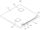
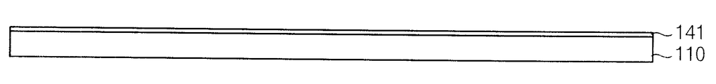
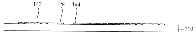
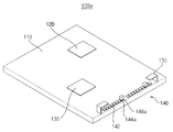
| KR20120107176A (ko) | 데이터 저장 장치 및 그의 제조 방법 | |
| US7972181B1 (en) | Compound female connector | |
| US9107333B1 (en) | Molded leadframe for PCB-to-PCB connection | |
| KR20080067745A (ko) | 다변환 젠더 | |
| US20150099398A1 (en) | Connector for printed circuit boards | |
| CN205451777U (zh) | 固态硬盘存储模块、固态硬盘组件及固态硬盘 | |
| JP2012198875A5 (enExample) | ||
| US7540751B2 (en) | Method for fabricating microconnector and shape of terminals thereof | |
| KR20040079780A (ko) | 메모리 확장을 위한 메모리 모듈의 제조방법 | |
| CN203596429U (zh) | 用来耦接第一电路板与第二电路板的电连接器 | |
| KR20100101401A (ko) | 플러그 컨넥터 일체형 인쇄 회로 기판 및 이를 포함한 전자장비 | |
| CN101383456A (zh) | 电子卡连接器 | |
| CN101162807B (zh) | 电连接器及其制造方法 | |
| CN101154998A (zh) | 总线系统 |
Legal Events
| Date | Code | Title | Description |
|---|---|---|---|
| PA0109 | Patent application |
Patent event code: PA01091R01D Comment text: Patent Application Patent event date: 20110321 |
|
| PG1501 | Laying open of application | ||
| A201 | Request for examination | ||
| PA0201 | Request for examination |
Patent event code: PA02012R01D Patent event date: 20160302 Comment text: Request for Examination of Application Patent event code: PA02011R01I Patent event date: 20110321 Comment text: Patent Application |
|
| E902 | Notification of reason for refusal | ||
| PE0902 | Notice of grounds for rejection |
Comment text: Notification of reason for refusal Patent event date: 20170327 Patent event code: PE09021S01D |
|
| E601 | Decision to refuse application | ||
| PE0601 | Decision on rejection of patent |
Patent event date: 20170911 Comment text: Decision to Refuse Application Patent event code: PE06012S01D Patent event date: 20170327 Comment text: Notification of reason for refusal Patent event code: PE06011S01I |