KR20120107176A - Data storage device and method of manufacturing the same - Google Patents
Data storage device and method of manufacturing the same Download PDFInfo
- Publication number
- KR20120107176A KR20120107176A KR1020110024705A KR20110024705A KR20120107176A KR 20120107176 A KR20120107176 A KR 20120107176A KR 1020110024705 A KR1020110024705 A KR 1020110024705A KR 20110024705 A KR20110024705 A KR 20110024705A KR 20120107176 A KR20120107176 A KR 20120107176A
- Authority
- KR
- South Korea
- Prior art keywords
- circuit board
- printed circuit
- cable
- tab
- dummy
- Prior art date
Links
Images


Classifications
-
- H—ELECTRICITY
- H01—ELECTRIC ELEMENTS
- H01R—ELECTRICALLY-CONDUCTIVE CONNECTIONS; STRUCTURAL ASSOCIATIONS OF A PLURALITY OF MUTUALLY-INSULATED ELECTRICAL CONNECTING ELEMENTS; COUPLING DEVICES; CURRENT COLLECTORS
- H01R12/00—Structural associations of a plurality of mutually-insulated electrical connecting elements, specially adapted for printed circuits, e.g. printed circuit boards [PCB], flat or ribbon cables, or like generally planar structures, e.g. terminal strips, terminal blocks; Coupling devices specially adapted for printed circuits, flat or ribbon cables, or like generally planar structures; Terminals specially adapted for contact with, or insertion into, printed circuits, flat or ribbon cables, or like generally planar structures
- H01R12/70—Coupling devices
- H01R12/7005—Guiding, mounting, polarizing or locking means; Extractors
-
- G—PHYSICS
- G11—INFORMATION STORAGE
- G11B—INFORMATION STORAGE BASED ON RELATIVE MOVEMENT BETWEEN RECORD CARRIER AND TRANSDUCER
- G11B33/00—Constructional parts, details or accessories not provided for in the other groups of this subclass
- G11B33/12—Disposition of constructional parts in the apparatus, e.g. of power supply, of modules
-
- H—ELECTRICITY
- H01—ELECTRIC ELEMENTS
- H01R—ELECTRICALLY-CONDUCTIVE CONNECTIONS; STRUCTURAL ASSOCIATIONS OF A PLURALITY OF MUTUALLY-INSULATED ELECTRICAL CONNECTING ELEMENTS; COUPLING DEVICES; CURRENT COLLECTORS
- H01R12/00—Structural associations of a plurality of mutually-insulated electrical connecting elements, specially adapted for printed circuits, e.g. printed circuit boards [PCB], flat or ribbon cables, or like generally planar structures, e.g. terminal strips, terminal blocks; Coupling devices specially adapted for printed circuits, flat or ribbon cables, or like generally planar structures; Terminals specially adapted for contact with, or insertion into, printed circuits, flat or ribbon cables, or like generally planar structures
- H01R12/70—Coupling devices
- H01R12/71—Coupling devices for rigid printing circuits or like structures
- H01R12/712—Coupling devices for rigid printing circuits or like structures co-operating with the surface of the printed circuit or with a coupling device exclusively provided on the surface of the printed circuit
- H01R12/716—Coupling device provided on the PCB
- H01R12/718—Contact members provided on the PCB without an insulating housing
-
- H—ELECTRICITY
- H01—ELECTRIC ELEMENTS
- H01R—ELECTRICALLY-CONDUCTIVE CONNECTIONS; STRUCTURAL ASSOCIATIONS OF A PLURALITY OF MUTUALLY-INSULATED ELECTRICAL CONNECTING ELEMENTS; COUPLING DEVICES; CURRENT COLLECTORS
- H01R12/00—Structural associations of a plurality of mutually-insulated electrical connecting elements, specially adapted for printed circuits, e.g. printed circuit boards [PCB], flat or ribbon cables, or like generally planar structures, e.g. terminal strips, terminal blocks; Coupling devices specially adapted for printed circuits, flat or ribbon cables, or like generally planar structures; Terminals specially adapted for contact with, or insertion into, printed circuits, flat or ribbon cables, or like generally planar structures
- H01R12/70—Coupling devices
- H01R12/71—Coupling devices for rigid printing circuits or like structures
- H01R12/72—Coupling devices for rigid printing circuits or like structures coupling with the edge of the rigid printed circuits or like structures
- H01R12/721—Coupling devices for rigid printing circuits or like structures coupling with the edge of the rigid printed circuits or like structures cooperating directly with the edge of the rigid printed circuits
Landscapes
- Details Of Connecting Devices For Male And Female Coupling (AREA)
- Coupling Device And Connection With Printed Circuit (AREA)
- Combinations Of Printed Boards (AREA)
Abstract
Description
본 발명은 데이터 저장 장치 및 그의 제조 방법에 관한 것으로서, 보다 구체적으로는 외장 하드와 같은 데이터 저장 장치 및 이러한 데이터 저장 장치를 제조하는 방법에 관한 것이다.TECHNICAL FIELD The present invention relates to a data storage device and a method for manufacturing the same, and more particularly, to a data storage device such as an external hard disk and a method for manufacturing such data storage device.
일반적으로, 정보화 시대의 도래와 함께 개인이 저장하고 이동해야 할 데이터의 양도 급격하게 증가하고 있는 추세이다. 데이터의 양의 증가에 따라, 여러 가지 종류의 데이터 저장 장치들이 개발되고 있다.In general, with the advent of the information age, the amount of data that an individual needs to store and move is rapidly increasing. As the amount of data increases, various kinds of data storage devices are being developed.
데이터 저장 장치의 대표적인 예가 하드 디스크 드라이브(hard disk drive)이다. 하드 디스크 드라이브는 높은 기록 밀도, 높은 데이터 전송 속도, 빠른 데이터 접근 시간(access time), 및 낮은 가격 등의 장점으로 인해 널리 사용되고 있다. 그러나, 하드 디스크 드라이브는 복잡한 기계적 구조를 갖고 있기 때문에, 작은 충격과 진동에도 쉽게 고장이 발생되는 문제가 있다.A representative example of a data storage device is a hard disk drive. Hard disk drives are widely used because of their high recording density, high data transfer speed, fast data access time, and low cost. However, since the hard disk drive has a complicated mechanical structure, there is a problem that failure occurs easily even with a small shock and vibration.
최근에는, 플래시 메모리를 갖는 솔리드 스테이트 드라이브(solid state drive)가 하드 디스크 드라이브 대신에 널리 사용되고 있다. 솔리드 스테이트 드라이브는 하드 디스크 드라이브와는 달리 기계적 구조를 갖고 있지 않다. 따라서, 솔리드 스테이트 드라이브는 하드 디스크 드라이브에 비해서 짧은 구동 시간 및 지연 시간을 갖는다. 특히, 솔리드 스테이트 드라이브는 외부 충격에 강한 구조를 갖고 있어서, 휴대형 데이터 저장 장치로서 널리 사용되고 있다.In recent years, solid state drives with flash memory have been widely used in place of hard disk drives. Solid state drives, unlike hard disk drives, do not have a mechanical structure. Thus, solid state drives have shorter run times and delay times compared to hard disk drives. In particular, the solid state drive has a structure resistant to external shocks, and thus is widely used as a portable data storage device.
솔리드 스테이트 드라이브와 호스트 간의 데이터 전송을 위한 인터페이스로서 ATA(advanced technology attachment) 인터페이스가 사용되고 있다. ATA 인터페이스는 parallel-ATA(PATA) 방식과 serial-ATA(SATA) 방식으로 구분할 수 있다. PATA 인터페이스보다 전송 속도가 빠른 SATA 인터페이스가 주로 사용되고 있다.An advanced technology attachment (ATA) interface is used as an interface for data transmission between the solid state drive and the host. The ATA interface can be classified into a parallel-ATA (PATA) method and a serial-ATA (SATA) method. The SATA interface, which is faster than the PATA interface, is mainly used.
솔리드 스테이트 드라이브는 SATA 케이블을 매개로 호스트와 연결된다. 따라서, 솔리드 스테이트 드라이브는 메모리 칩이 실장된 인쇄회로기판, 및 인쇄회로기판에 실장되어 SATA 케이블과의 접속을 위한 커넥터를 갖는다. 커넥터는 SATA 케이블의 진입 방향을 안내하기 위한 가이드를 갖는다.Solid state drives are connected to the host via SATA cables. Thus, the solid state drive has a printed circuit board on which a memory chip is mounted, and a connector mounted on the printed circuit board for connection with a SATA cable. The connector has a guide for guiding the entry direction of the SATA cable.
최근, 커넥터를 별도로 제작하지 않고, 인쇄회로기판에 일체로 형성하기 위한 방안들이 제안되고 있다. 그러나, SATA 케이블과 접촉하는 탭(tab)의 형성은 용이하지만, 제작의 복잡함, 제작 비용 등의 문제로 인해서 가이드 형성에 곤란한 점이 많았다.In recent years, methods for integrally forming a printed circuit board without producing a connector have been proposed. However, although the formation of tabs in contact with SATA cables is easy, there are many difficulties in forming guides due to problems such as manufacturing complexity and manufacturing cost.
본 발명은 저렴한 비용으로 제조 가능한 별도의 커넥터를 갖지 않는 데이터 저장 장치를 제공한다.The present invention provides a data storage device that does not have a separate connector that can be manufactured at low cost.
또한, 본 발명은 상기된 데이터 저장 장치를 제조하기 위한 방법을 제공한다.The present invention also provides a method for manufacturing the data storage device described above.
본 발명의 일 견지에 따른 데이터 저장 장치는 인쇄회로기판, 연결 탭, 더미 탭 및 가이드를 포함한다. 메모리 칩이 인쇄회로기판에 실장된다. 연결 탭은 상기 인쇄회로기판의 제 1 면에 형성되어, 상기 인쇄회로기판을 케이블과 전기적으로 연결시킨다. 더미 탭은 상기 인쇄회로기판의 제 1 면에 형성된다. 가이드는 상기 더미 탭 상에 형성되어, 상기 케이블의 진입 방향을 안내한다.A data storage device according to an aspect of the present invention includes a printed circuit board, a connection tab, a dummy tab, and a guide. The memory chip is mounted on the printed circuit board. A connection tab is formed on the first side of the printed circuit board to electrically connect the printed circuit board with a cable. The dummy tab is formed on the first surface of the printed circuit board. A guide is formed on the dummy tab to guide the entry direction of the cable.
본 발명의 일 실시예에 따르면, 상기 더미 탭은 상기 연결 탭과 동일한 물질을 포함할 수 있다. 상기 가이드는 절연 물질을 포함할 수 있다.According to an embodiment of the present invention, the dummy tab may include the same material as the connection tab. The guide may comprise an insulating material.
본 발명의 다른 실시예에 따르면, 상기 케이블은 SATA(serial advanced technology attachment) 케이블을 포함하고, 상기 가이드 부재는 인접하게 배치된 한 쌍으로 이루어질 수 있다. 또는, 상기 케이블은 μ-SATA(micro serial advanced technology attachment) 케이블을 포함하고, 상기 가이드 부재는 상기 연결 탭을 사이에 두고 배치된 한 쌍으로 이루어질 수 있다.According to another embodiment of the present invention, the cable may include a serial advanced technology attachment (SATA) cable, and the guide member may be formed in a pair disposed adjacently. Alternatively, the cable may include a micro serial advanced technology attachment (μSATA) cable, and the guide member may be formed in a pair disposed with the connection tab interposed therebetween.
본 발명의 또 다른 실시예에 따르면, 데이터 저장 장치는 상기 제 1 면과 반대측인 상기 인쇄회로기판의 제 2 면에 형성되어 상기 인쇄회로기판을 상기 케이블과 다른 종류의 제 2 케이블과 전기적으로 연결시키기 위한 제 2 연결 탭(connection tab), 및 상기 인쇄회로기판의 제 2 면에 형성된 제 2 더미 탭을 더 포함할 수 있다. 또한, 데이터 저장 장치는 상기 제 2 더미 탭 상에 선택적으로 형성되어, 상기 제 2 케이블의 진입 방향을 안내하기 위한 제 2 가이드를 더 포함할 수 있다. 상기 케이블은 SATA(serial advanced technology attachment) 케이블을 포함하고, 상기 제 2 케이블은 μ-SATA(micro serial advanced technology attachment) 케이블을 포함할 수 있다.According to another embodiment of the present invention, a data storage device is formed on a second surface of the printed circuit board opposite to the first surface to electrically connect the printed circuit board with a second cable of a different type from the cable. And a second dummy tab formed on the second surface of the printed circuit board. In addition, the data storage device may further include a second guide selectively formed on the second dummy tab to guide the entry direction of the second cable. The cable may include a serial advanced technology attachment (SATA) cable, and the second cable may include a micro serial advanced technology attachment (SATA) cable.
본 발명의 또 다른 실시예에 따르면, 데이터 저장 장치는 상기 인쇄회로기판에 형성되어, 상기 케이블을 수용하는 하우징을 더 포함할 수 있다.According to another embodiment of the present invention, the data storage device may further include a housing formed on the printed circuit board to accommodate the cable.
본 발명의 다른 견지에 따른 데이터 저장 장치는 인쇄회로기판, 제 1 연결 탭, 제 1 더미 탭, 제 1 가이드, 제 2 연결 탭, 제 2 더미 탭 및 제 2 가이드를 포함한다. 메모리 칩이 인쇄회로기판에 실장된다. 제 1 연결 탭은 상기 인쇄회로기판의 제 1 면에 형성되어, 상기 인쇄회로기판을 SATA 케이블과 전기적으로 연결시킨다. 제 1 더미 탭은 상기 인쇄회로기판의 제 1 면에 형성된다. 제 1 가이드는 상기 더미 탭 상에 선택적으로 형성되어, 상기 SATA 케이블의 진입 방향을 안내한다. 제 2 연결 탭은 상기 제 1 면과 반대측인 상기 인쇄회로기판의 제 2 면에 형성되어, 상기 인쇄회로기판을 μ-SATA 케이블과 전기적으로 연결시킨다. 제 2 더미 탭은 상기 인쇄회로기판의 제 2 면에 형성된다. 제 2 가이드는 상기 제 2 더미 탭 상에 선택적으로 형성되어, 상기 μ-SATA 케이블의 진입 방향을 안내한다.According to another aspect of the present invention, a data storage device includes a printed circuit board, a first connection tab, a first dummy tab, a first guide, a second connection tab, a second dummy tab, and a second guide. The memory chip is mounted on the printed circuit board. A first connection tab is formed on the first side of the printed circuit board to electrically connect the printed circuit board with the SATA cable. The first dummy tab is formed on the first surface of the printed circuit board. A first guide is selectively formed on the dummy tab to guide the entry direction of the SATA cable. A second connection tab is formed on the second surface of the printed circuit board opposite to the first surface to electrically connect the printed circuit board with the μ-SATA cable. The second dummy tab is formed on the second surface of the printed circuit board. A second guide is optionally formed on the second dummy tab to guide the entry direction of the μ-SATA cable.
본 발명의 일 실시예에 따르면, 데이터 저장 장치는 상기 인쇄회로기판에 형성되어, 상기 케이블을 수용하는 하우징을 더 포함할 수 있다.According to an embodiment of the present invention, the data storage device may further include a housing formed on the printed circuit board to accommodate the cable.
본 발명의 또 다른 견지에 따른 데이터 저장 장치는 인쇄회로기판 및 커넥터를 포함한다. 메모리 칩이 인쇄회로기판에 실장된다. 커넥터는 상기 인쇄회로기판에 일체로 형성되어 상기 인쇄회로기판을 SATA 케이블과 전기적으로 연결시킨다. 커넥터는 상기 SATA 케이블의 진입 방향을 안내하기 위한 가이드를 갖는다.A data storage device according to another aspect of the present invention includes a printed circuit board and a connector. The memory chip is mounted on the printed circuit board. The connector is integrally formed on the printed circuit board to electrically connect the printed circuit board to the SATA cable. The connector has a guide for guiding the entry direction of the SATA cable.
본 발명의 일 실시예에 따르면, 상기 커넥터는 상기 인쇄회로기판에 형성되어 상기 SATA 케이블과 전기적으로 연결되는 연결 탭(connection tab), 상기 인쇄회로기판에 형성된 더미 탭(dummy tab), 및 상기 더미 탭 상에 형성된 상기 가이드를 포함할 수 있다.According to an embodiment of the present invention, the connector is formed on the printed circuit board (connection tab) that is electrically connected to the SATA cable, a dummy tab formed on the printed circuit board, and the dummy It may include the guide formed on the tab.
본 발명의 또 다른 견지에 따른 데이터 저장 장치는 인쇄회로기판 및 커넥터를 포함한다. 메모리 칩이 인쇄회로기판에 실장된다. 커넥터는 상기 인쇄회로기판에 일체로 형성되어 상기 인쇄회로기판을 μ-SATA 케이블과 전기적으로 연결시킨다. 커넥터는 상기 μ-SATA 케이블의 진입 방향을 안내하기 위한 가이드를 갖는다.A data storage device according to another aspect of the present invention includes a printed circuit board and a connector. The memory chip is mounted on the printed circuit board. The connector is integrally formed on the printed circuit board to electrically connect the printed circuit board with a μ-SATA cable. The connector has a guide for guiding the entry direction of the μ-SATA cable.
본 발명의 일 실시예에 따르면, 상기 커넥터는 상기 인쇄회로기판에 형성되어 상기 μ-SATA 케이블과 전기적으로 연결되는 연결 탭(connection tab), 상기 인쇄회로기판에 형성된 더미 탭(dummy tab), 및 상기 더미 탭 상에 형성된 상기 가이드를 포함할 수 있다.According to an embodiment of the present invention, the connector is formed on the printed circuit board (connection tab) that is electrically connected to the μ-SATA cable, a dummy tab formed on the printed circuit board, and It may include the guide formed on the dummy tab.
본 발명의 또 다른 견지에 따른 데이터 저장 장치의 제조 방법에 따르면, 인쇄회로기판의 제 1 면에 상기 인쇄회로기판을 케이블과 전기적으로 연결시키기 위한 연결 탭(connection tab)을 형성한다. 상기 인쇄회로기판의 제 1 면에 더미 탭을 형성한다. 상기 더미 탭 상에 상기 케이블의 진입 방향을 안내하기 위한 가이드를 형성한다.According to a method of manufacturing a data storage device according to another aspect of the present invention, a connection tab for electrically connecting the printed circuit board with a cable is formed on the first side of the printed circuit board. A dummy tab is formed on the first surface of the printed circuit board. A guide for guiding the entry direction of the cable is formed on the dummy tab.
본 발명의 일 실시예에 따르면, 상기 연결 탭을 형성하는 단계는 상기 더미 탭을 형성하는 단계와 동시에 이루어질 수 있다. 상기 연결 탭과 상기 더미 탭을 동시에 형성하는 단계는 상기 인쇄회로기판의 제 1 면에 도전막을 형성하는 단계, 및 상기 도전막을 패터닝하여, 상기 연결 탭과 상기 더미 탭을 형성하는 단계를 포함할 수 있다.According to an embodiment of the present disclosure, the forming of the connection tab may be performed at the same time as the forming of the dummy tab. Forming the connection tab and the dummy tab simultaneously may include forming a conductive film on the first surface of the printed circuit board, and patterning the conductive film to form the connection tab and the dummy tab. have.
본 발명의 다른 실시예에 따르면, 상기 제조 방법은 상기 제 1 면과 반대측인 상기 인쇄회로기판의 제 2 면에 상기 인쇄회로기판을 상기 케이블과 다른 종류의 제 2 케이블과 전기적으로 연결시키기 위한 제 2 연결 탭(connection tab)을 형성하는 단계, 및 상기 인쇄회로기판의 제 2 면에 제 2 더미 탭을 형성하는 단계를 더 포함할 수 있다. 또한, 상기 제조 방법은 상기 제 2 더미 탭 상에 상기 제 2 케이블의 진입 방향을 안내하기 위한 제 2 가이드 부재를 선택적으로 형성하는 단계를 더 포함할 수 있다.According to another embodiment of the present invention, the manufacturing method includes a method for electrically connecting the printed circuit board with a second cable of a different type from the cable on the second surface of the printed circuit board opposite to the first surface. The method may further include forming a connection tab, and forming a second dummy tab on the second surface of the printed circuit board. In addition, the manufacturing method may further comprise the step of selectively forming a second guide member for guiding the entry direction of the second cable on the second dummy tab.
본 발명의 또 다른 실시예에 따르면, 상기 제조 방법은 상기 인쇄회로기판에 상기 케이블을 수용하는 하우징을 형성하는 단계를 더 포함할 수 있다.According to another embodiment of the present invention, the manufacturing method may further comprise forming a housing for accommodating the cable on the printed circuit board.
상기와 같은 본 발명에 따르면, 연결 탭과 같이 형성된 더미 탭 상에 절연 물질을 배치하는 간단한 공정을 통해서 케이블의 진입 방향을 안내하는 가이드를 형성할 수 있다. 따라서, 별도의 커넥터를 갖지 않는 데이터 저장 장치를 간단한 공정을 통해서 저렴한 비용으로 제조할 수가 있게 된다.According to the present invention as described above, it is possible to form a guide for guiding the entry direction of the cable through a simple process of disposing an insulating material on the dummy tab formed as a connection tab. Therefore, a data storage device having no separate connector can be manufactured at low cost through a simple process.
도 1은 본 발명의 제 1 실시예에 따른 데이터 저장 장치를 나타낸 사시도이다.
도 2는 도 1의 데이터 저장 장치의 커넥터를 나타낸 단면도이다.
도 3 내지 도 6은 도 2의 데이터 저장 장치를 제조하는 방법을 순차적으로 나타낸 단면도들이다.
도 7은 본 발명의 제 2 실시예에 따른 데이터 저장 장치를 나타낸 사시도이다.
도 8은 도 7의 데이터 저장 장치의 커넥터를 나타낸 단면도이다.
도 9 내지 도 12는 도 8의 데이터 저장 장치를 제조하는 방법을 순차적으로 나타낸 단면도들이다.
도 13은 본 발명의 제 3 실시예에 따른 데이터 저장 장치를 나타낸 단면도이다.
도 14는 본 발명의 제 4 실시예에 따른 데이터 저장 장치를 나타낸 단면도이다.1 is a perspective view showing a data storage device according to a first embodiment of the present invention.
2 is a cross-sectional view illustrating a connector of the data storage device of FIG. 1.
3 to 6 are cross-sectional views sequentially illustrating a method of manufacturing the data storage device of FIG. 2.
7 is a perspective view showing a data storage device according to a second embodiment of the present invention.
8 is a cross-sectional view illustrating a connector of the data storage device of FIG. 7.
9 through 12 are cross-sectional views sequentially illustrating a method of manufacturing the data storage device of FIG. 8.
13 is a cross-sectional view illustrating a data storage device according to a third embodiment of the present invention.
14 is a cross-sectional view illustrating a data storage device according to a fourth embodiment of the present invention.
이하, 첨부한 도면들을 참조하여 본 발명의 바람직한 실시예들을 상세히 설명한다.Hereinafter, preferred embodiments of the present invention will be described in detail with reference to the accompanying drawings.
본 발명은 다양한 변경을 가할 수 있고 여러 가지 형태를 가질 수 있는 바, 특정 실시예들을 도면에 예시하고 본문에 상세하게 설명하고자 한다. 그러나, 이는 본 발명을 특정한 개시 형태에 대해 한정하려는 것이 아니며, 본 발명의 사상 및 기술 범위에 포함되는 모든 변경, 균등물 내지 대체물을 포함하는 것으로 이해되어야 한다. 각 도면을 설명하면서 유사한 참조부호를 유사한 구성요소에 대해 사용하였다.The present invention is capable of various modifications and various forms, and specific embodiments are illustrated in the drawings and described in detail in the text. It should be understood, however, that the invention is not intended to be limited to the particular forms disclosed, but includes all modifications, equivalents, and alternatives falling within the spirit and scope of the invention. Like reference numerals are used for like elements in describing each drawing.
제1, 제2 등의 용어는 다양한 구성요소들을 설명하는데 사용될 수 있지만, 상기 구성요소들은 상기 용어들에 의해 한정되어서는 안 된다. 상기 용어들은 하나의 구성요소를 다른 구성요소로부터 구별하는 목적으로만 사용된다. 예를 들어, 본 발명의 권리 범위를 벗어나지 않으면서 제1 구성요소는 제2 구성요소로 명명될 수 있고, 유사하게 제2 구성요소도 제1 구성요소로 명명될 수 있다.The terms first, second, etc. may be used to describe various components, but the components should not be limited by the terms. The terms are used only for the purpose of distinguishing one component from another. For example, without departing from the scope of the present invention, the first component may be referred to as a second component, and similarly, the second component may also be referred to as a first component.
본 출원에서 사용한 용어는 단지 특정한 실시예를 설명하기 위해 사용된 것으로, 본 발명을 한정하려는 의도가 아니다. 단수의 표현은 문맥상 명백하게 다르게 뜻하지 않는 한, 복수의 표현을 포함한다. 본 출원에서, "포함하다" 또는 "가지다" 등의 용어는 명세서상에 기재된 특징, 숫자, 단계, 동작, 구성요소, 부분품 또는 이들을 조합한 것이 존재함을 지정하려는 것이지, 하나 또는 그 이상의 다른 특징들이나 숫자, 단계, 동작, 구성요소, 부분품 또는 이들을 조합한 것들의 존재 또는 부가 가능성을 미리 배제하지 않는 것으로 이해되어야 한다.The terminology used herein is for the purpose of describing particular example embodiments only and is not intended to be limiting of the present invention. Singular expressions include plural expressions unless the context clearly indicates otherwise. In this application, the terms "comprises", "having", and the like are used to specify that a feature, a number, a step, an operation, an element, a part or a combination thereof is described in the specification, But do not preclude the presence or addition of one or more other features, integers, steps, operations, components, parts, or combinations thereof.
다르게 정의되지 않는 한, 기술적이거나 과학적인 용어를 포함해서 여기서 사용되는 모든 용어들은 본 발명이 속하는 기술 분야에서 통상의 지식을 가진 자에 의해 일반적으로 이해되는 것과 동일한 의미를 가지고 있다. 일반적으로 사용되는 사전에 정의되어 있는 것과 같은 용어들은 관련 기술의 문맥 상 가지는 의미와 일치하는 의미를 가지는 것으로 해석되어야 하며, 본 출원에서 명백하게 정의하지 않는 한, 이상적이거나 과도하게 형식적인 의미로 해석되지 않는다.
Unless defined otherwise, all terms used herein, including technical or scientific terms, have the same meaning as commonly understood by one of ordinary skill in the art to which this invention belongs. Terms such as those defined in commonly used dictionaries are to be interpreted as having a meaning consistent with the contextual meaning of the related art and are to be interpreted as either ideal or overly formal in the sense of the present application Do not.
실시예 1Example 1
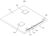
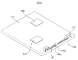
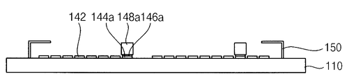
도 1은 본 발명의 제 1 실시예에 따른 데이터 저장 장치를 나타낸 사시도이고, 도 2는 도 1의 데이터 저장 장치의 커넥터를 나타낸 단면도이다.1 is a perspective view illustrating a data storage device according to a first embodiment of the present invention, and FIG. 2 is a cross-sectional view illustrating a connector of the data storage device of FIG. 1.
도 1 및 도 2를 참조하면, 본 실시예에 따른 데이터 저장 장치(100)는 인쇄회로기판(110:printed circuit board:PCB), 및 커넥터(140)를 포함한다.1 and 2, the
본 실시예에서, 데이터 저장 장치(100)는 외장 하드 디스크 드라이브와 같은 불휘발성 저장 매체를 포함할 수 있다. 예를 들어서, 데이터 저장 장치(100)는 NANA 플래시 메모리를 갖는 솔리드 스테이트 드라이브(solid state drive:SSD)를 포함할 수 있다.In the present embodiment, the
인쇄회로기판(110)은 회로 패턴(미도시)들을 갖는다. NAND 플래시 메모리 칩 등과 같은 메모리 칩(120)들이 인쇄회로기판(110)의 제 1 면에 실장된다. 또한, 컨트롤러 칩(130)이 인쇄회로기판(110)의 제 1 면에 실장된다. 메모리 칩(120)과 컨트롤러 칩(130)은 인쇄회로기판(110)의 회로 패턴과 전기적으로 연결된다.The printed
커넥터(140)는 인쇄회로기판(110)의 측부에 형성된다. 커넥터(140)는 인쇄회로기판(110)을 컴퓨터 등과 같은 호스트에 전기적으로 연결시켜 주기 위한 매개체로서의 역할을 한다. 따라서, 케이블(미도시)이 커넥터(140)에 삽입되어, 인쇄회로기판(110)의 회로 패턴과 전기적으로 연결된다.The
본 실시예에서, 케이블은 SATA 케이블을 포함할 수 있다. SATA 케이블은 복수개의 탭들, 및 가이드 슬롯을 갖는다. 탭들은 커넥터(140)를 매개로 인쇄회로기판(110)의 회로 패턴과 전기적으로 연결된다. 가이드 슬롯은 커넥터(140)의 가이드(148)가 삽입될 수 있는 형상을 가져서, 커넥터(140) 내로의 SATA 케이블의 진입 방향을 안내한다. SATA 케이블의 가이드 슬롯은 표준화된 규격으로서, 인접하게 배치된 한 쌍으로 이루어진다.In this embodiment, the cable may comprise a SATA cable. The SATA cable has a plurality of tabs and a guide slot. The tabs are electrically connected to the circuit pattern of the printed
본 실시예에서, 커넥터(140)는 인쇄회로기판(110)에 실장되는 별도의 부품이 아니라, 인쇄회로기판(110)에 일체로 형성된다. 커넥터(140)는 복수개의 연결 탭(142), 더미 탭(144) 및 가이드(148)를 포함한다.In the present embodiment, the
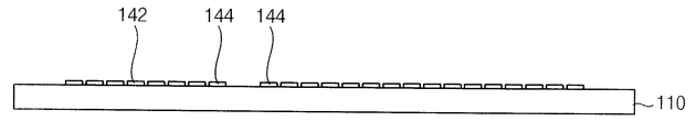
연결 탭(142)들은 인쇄회로기판(110)의 제 1 면 측부에 배열된다. 연결 탭(142)은 인쇄회로기판(142)의 회로 패턴과 전기적으로 연결된다. 또한, 연결 탭(142)들은 SATA 케이블의 탭들과 전기적으로 접촉한다.The
더미 탭(144)들은 인쇄회로기판(110)의 제 1 면 측부에 배열된다. 본 실시예에서, 더미 탭(144)들은 연결 탭(142)들의 사이에 위치한 한 쌍으로 이루어진다. 더미 탭(144)들의 위치는 규격화된 SATA 케이블의 가이드 슬롯들의 위치와 대응한다. 본 실시예에서, 더미 탭(144)들은 연결 탭(142)과 실질적으로 동일한 물질을 포함할 수 있다. 예를 들어서, 연결 탭(142)과 더미 탭(144)들은 구리를 포함할 수 있다. 또한, 더미 탭(144)들은 연결 탭(142)을 형성하는 공정으로부터 동시에 형성될 수 있다. 즉, 더미 탭(144)들은 별도의 공정을 통해서 형성되는 것이 아니라, 연결 탭(142)의 형성 공정과 함께 형성된 연결 탭(142)의 일부에 해당한다. 본 실시예에서, 더미 탭(144)은 데이터 저장 장치(100)와 호스트 간의 전기적 연결 매개체로서의 기능을 갖고 있지 않으므로, 인쇄회로기판(110)의 회로 패턴과 전기적으로 연결되지 않는다. 다른 실시예로서, 더미 탭(144)은 SATA 케이블의 탭과 전기적으로 연결되지 않으므로, 더미 탭(144)은 인쇄회로기판(110)의 회로 패턴과 전기적으로 연결될 수도 있다.The
한 쌍의 가이드(148)들이 더미 탭(144)들 상에 형성된다. 전술한 바와 같이, 가이드(148)들은 SATA 케이블의 가이드 슬롯에 삽입되어, SATA 케이블의 진입 방향을 안내한다. 따라서, 가이드(148)들의 위치와 형상은 규격화된 SATA 케이블의 가이드 슬롯의 위치와 형상에 각각 대응한다. 본 실시예에서, 가이드(148)들은 솔더 조인트(146)들을 매개로 더미 탭(144)들 상에 부착될 수 있다. 또한, 가이드(148)들은 에폭시 몰딩 컴파운드(epoxy molding compound:EMC) 등과 같은 절연 물질을 포함할 수 있다.A pair of
부가적으로, 하우징(150)이 인쇄회로기판(110)의 제 1 면에 형성될 수 있다. 하우징(150)은 SATA 케이블을 수용하는 형상을 가져서, 가이드(148))들이 SATA 케이블의 가이드 슬롯에 용이하게 삽입될 수 있도록 한다.In addition, the
본 실시예에서는, 케이블이 SATA 케이블을 포함하는 것으로 예시하였다. 이에 따라, 더미 탭(144)과 가이드(148)가 규격화된 SATA 케이블의 형상과 대응하는 형상을 갖는다. 그러나, 인쇄회로기판(110)에 일체로 형성된 더미 탭(144)과 가이드(148)를 포함하는 커넥터(140)는 다른 종류의 케이블들에도 적용될 수 있음은 물론이다.In this embodiment, the cable is illustrated as including a SATA cable. Accordingly, the
도 3 내지 도 6은 도 2의 데이터 저장 장치를 제조하는 방법을 순차적으로 나타낸 단면도들이다.3 to 6 are cross-sectional views sequentially illustrating a method of manufacturing the data storage device of FIG. 2.
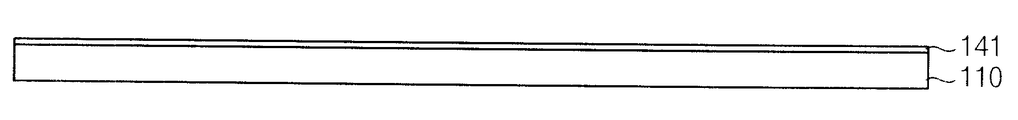
도 3을 참조하면, 도전막(141)을 인쇄회로기판(110)의 제 1 면에 형성한다. 본 실시예에서, 도전막(141)은 구리막을 포함할 수 있다.Referring to FIG. 3, a
도 4를 참조하면, 도전막(141)을 패터닝하여 연결 탭(142)들과 더미 탭(144)들을 동시에 형성한다. 본 실시예에서, 포토레지스트 패턴(미도시)을 도전막(141) 상에 형성한다. 포토레지스트 패턴을 식각 마스크로 사용하여 도전막(141)을 식각함으로써, 연결 탭(142)들과 더미 탭(144)들을 동시에 형성할 수 있다. 더미 탭(144)은 SATA 케이블의 규격과 대응하도록 인접하게 배치된 한 쌍으로 이루어진다. 연결 탭(142)들은 인쇄회로기판(110)의 회로 패턴과 전기적으로 연결된다. 반면에, 더미 탭(144)들은 인쇄회로기판(110)의 회로 패턴과 절연된다.Referring to FIG. 4, the
도 5를 참조하면, 접착제(146)를 더미 탭(144)들 상에 형성한다. 본 실시예에서, 접착제(146)는 솔더 조인트를 포함할 수 있다.Referring to FIG. 5, an adhesive 146 is formed on the
도 6을 참조하면, 가이드(148)들을 접착제(146)를 매개로 더미 탭(144)들 상에 부착한다. 가이드(148)들은 EMC 등과 같은 절연 물질을 포함할 수 있다. 가이드(148)들은 SATA 케이블의 가이드 슬롯들에 삽입될 수 있는 형상을 갖는다.Referring to FIG. 6, the
SATA 케이블을 수용하는 형상을 갖는 하우징(150)을 인쇄회로기판(110)의 제 1 면에 형성하여, 도 2에 도시된 데이터 저장 장치(100)를 완성한다.A
본 실시예에 따르면, 연결 탭과 같이 형성된 더미 탭 상에 절연 물질을 배치하는 간단한 공정을 통해서 SATA 케이블의 진입 방향을 안내하는 가이드를 형성할 수 있다. 따라서, 일체형 커넥터를 갖는 데이터 저장 장치를 간단한 공정을 통해서 저렴한 비용으로 제조할 수가 있게 된다.
According to the present exemplary embodiment, a guide for guiding the entry direction of the SATA cable may be formed through a simple process of disposing an insulating material on the dummy tab formed as the connection tab. Therefore, a data storage device having an integrated connector can be manufactured at low cost through a simple process.
실시예 2Example 2
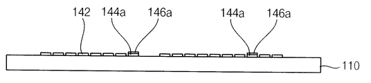
도 7은 본 발명의 제 2 실시예에 따른 데이터 저장 장치를 나타낸 사시도이고, 도 8은 도 7의 데이터 저장 장치의 커넥터를 나타낸 단면도이다.7 is a perspective view illustrating a data storage device according to a second exemplary embodiment of the present invention, and FIG. 8 is a cross-sectional view illustrating a connector of the data storage device of FIG. 7.
본 실시예에 따른 데이터 저장 장치(100a)는 커넥터(140a)를 제외하고는 실시예 1에 따른 데이터 저장 장치(100)의 구성요소들과 실질적으로 동일한 구성요소들을 포함한다. 따라서, 동일한 구성요소들은 동일한 참조부호들로 나타내고, 또한 동일한 구성요소들에 대한 반복 설명은 생략한다.The
도 7 및 도 8을 참조하면, 본 실시예에 따른 데이터 저장 장치(100a)는 인쇄회로기판(110:printed circuit board:PCB), 및 커넥터(140a)를 포함한다.7 and 8, the
커넥터(140a)는 인쇄회로기판(110)의 측부에 형성된다. 본 실시예에서, 케이블은 μ-SATA 케이블을 포함할 수 있다. μ-SATA 케이블은 복수개의 탭들, 및 가이드 슬롯을 갖는다. 탭들은 커넥터(140a)를 매개로 인쇄회로기판(110)의 회로 패턴과 전기적으로 연결된다. 가이드 슬롯은 커넥터(140a)의 가이드(148a)가 삽입될 수 있는 형상을 가져서, 커넥터(140a) 내로의 μ-SATA 케이블의 진입 방향을 안내한다. μ-SATA 케이블의 가이드 슬롯은 표준화된 규격으로서, 멀리 배치된 한 쌍으로 이루어진다.The connector 140a is formed at the side of the printed
본 실시예에서, 커넥터(140a)는 인쇄회로기판(110)에 실장되는 별도의 부품이 아니라, 인쇄회로기판(110)에 일체로 형성된다. 커넥터(140a)는 복수개의 연결 탭(142a), 더미 탭(144a) 및 가이드(148a)를 포함한다.In the present embodiment, the connector 140a is integrally formed on the printed
연결 탭(142a)들은 인쇄회로기판(110)의 제 1 면 측부에 배열된다. 연결 탭(142a)은 인쇄회로기판(142)의 회로 패턴과 전기적으로 연결된다. 또한, 연결 탭(142a)들은 μ-SATA 케이블의 탭들과 전기적으로 접촉한다.The connection tabs 142a are arranged at the side of the first surface of the printed
더미 탭(144a)들은 인쇄회로기판(110)의 제 1 면 측부에 배열된다. 본 실시예에서, 더미 탭(144a)들은 연결 탭(142a)들을 사이에 두고 배치된 한 쌍으로 이루어진다. 더미 탭(144a)들의 위치는 규격화된 μ-SATA 케이블의 가이드 슬롯들의 위치와 대응한다. 본 실시예에서, 더미 탭(144a)들은 연결 탭(142a)과 실질적으로 동일한 물질을 포함할 수 있다. 예를 들어서, 연결 탭(142a)과 더미 탭(144a)들은 구리를 포함할 수 있다. 또한, 더미 탭(144a)들은 연결 탭(142a)을 형성하는 공정으로부터 동시에 형성될 수 있다. 더미 탭(144a)은 데이터 저장 장치(100a)와 호스트 간의 전기적 연결 매개체로서의 기능을 갖고 있지 않으므로, 인쇄회로기판(110)의 회로 패턴과 전기적으로 연결되지 않는다.The
한 쌍의 가이드(148a)들이 더미 탭(144a)들 상에 형성된다. 전술한 바와 같이, 가이드(148a)들은 μ-SATA 케이블의 가이드 슬롯에 삽입되어, μ-SATA 케이블의 진입 방향을 안내한다. 따라서, 가이드(148a)들의 위치와 형상은 규격화된 μ-SATA 케이블의 가이드 슬롯의 위치와 형상에 각각 대응한다. 본 실시예에서, 가이드(148a)들은 솔더 조인트(146a)들을 매개로 더미 탭(144a)들 상에 부착될 수 있다. 또한, 가이드(148a)들은 에폭시 몰딩 컴파운드(epoxy molding compound:EMC) 등과 같은 절연 물질을 포함할 수 있다.A pair of
본 실시예에서는, 케이블이 μ-SATA 케이블을 포함하는 것으로 예시하였다. 이에 따라, 더미 탭(144a)과 가이드(148a)가 규격화된 μ-SATA 케이블의 형상과 대응하는 형상을 갖는다. 그러나, 인쇄회로기판(110)에 일체로 형성된 더미 탭(144a)과 가이드(148a)를 포함하는 커넥터(140a)는 다른 종류의 케이블들에도 적용될 수 있음은 물론이다.In this example, the cable is illustrated as including a μ-SATA cable. Accordingly, the
도 9 내지 도 12는 도 8의 데이터 저장 장치를 제조하는 방법을 순차적으로 나타낸 단면도들이다.9 through 12 are cross-sectional views sequentially illustrating a method of manufacturing the data storage device of FIG. 8.
도 9를 참조하면, 도전막(141a)을 인쇄회로기판(110)의 제 1 면에 형성한다. 본 실시예에서, 도전막(141a)은 구리막을 포함할 수 있다.Referring to FIG. 9, a
도 10을 참조하면, 도전막(141a)을 패터닝하여 연결 탭(142a)들과 더미 탭(144a)들을 동시에 형성한다. 본 실시예에서, 포토레지스트 패턴(미도시)을 도전막(141a) 상에 형성한다. 포토레지스트 패턴을 식각 마스크로 사용하여 도전막(141a)을 식각함으로써, 연결 탭(142a)들과 더미 탭(144a)들을 동시에 형성할 수 있다. 더미 탭(144a)은 μ-SATA 케이블의 규격과 대응하도록 연결 탭(142a)들을 사이에 두고 배치된 한 쌍으로 이루어진다. 연결 탭(142a)들은 인쇄회로기판(110)의 회로 패턴과 전기적으로 연결된다. 반면에, 더미 탭(144a)들은 인쇄회로기판(110)의 회로 패턴과 절연된다.Referring to FIG. 10, the
도 11을 참조하면, 접착제(146a)를 더미 탭(144a)들 상에 형성한다. 본 실시예에서, 접착제(146a)는 솔더 조인트를 포함할 수 있다.Referring to FIG. 11, an adhesive 146a is formed on the
도 12를 참조하면, 가이드(148a)들을 접착제(146a)를 매개로 더미 탭(144a)들 상에 부착한다. 가이드(148a)들은 EMC 등과 같은 절연 물질을 포함할 수 있다. 가이드(148a)들은 μ-SATA 케이블의 가이드 슬롯들에 삽입될 수 있는 형상을 갖는다.Referring to FIG. 12, the
μ-SATA 케이블을 수용하는 형상을 갖는 하우징(150a)을 인쇄회로기판(110)의 제 1 면에 형성하여, 도 8에 도시된 데이터 저장 장치(100)를 완성한다.A housing 150a having a shape for accommodating the μ-SATA cable is formed on the first surface of the printed
본 실시예에 따르면, 연결 탭과 같이 형성된 더미 탭 상에 절연 물질을 배치하는 간단한 공정을 통해서 μ-SATA 케이블의 진입 방향을 안내하는 가이드를 형성할 수 있다. 따라서, 일체형 커넥터를 갖는 데이터 저장 장치를 간단한 공정을 통해서 저렴한 비용으로 제조할 수가 있게 된다.
According to the present embodiment, a guide for guiding the entry direction of the μ-SATA cable may be formed through a simple process of disposing an insulating material on the dummy tab formed as the connection tab. Therefore, a data storage device having an integrated connector can be manufactured at low cost through a simple process.
실시예 3Example 3
도 13은 본 발명의 제 3 실시예에 따른 데이터 저장 장치를 나타낸 단면도이다.13 is a cross-sectional view illustrating a data storage device according to a third embodiment of the present invention.
도 13을 참조하면, 본 실시예에 따른 데이터 저장 장치(200)는 인쇄회로기판(110:printed circuit board:PCB), 제 1 커넥터(140) 및 제 2 커넥터(140a)를 포함한다.Referring to FIG. 13, the
제 1 커넥터(140)는 인쇄회로기판(110)의 제 1 면 측부에 형성된다. 여기서, 제 1 커넥터(140)는 실시예 1의 커넥터와 실질적으로 동일한 구성요소들을 포함하므로, 제 1 커넥터(140)에 대한 반복 설명은 생략한다.The
제 2 커넥터(140a)는 제 1 면과 반대측인 인쇄회로기판(110)의 제 2 면 측부에 형성된다. 여기서, 제 2 커넥터(140a)는 실시예 2의 커넥터와 실질적으로 동일한 구성요소들을 포함하므로, 제 2 커넥터(140a)에 대한 반복 설명은 생략한다.The second connector 140a is formed on the second surface side of the printed
본 실시예에서, 케이블은 SATA 케이블을 포함할 수 있다. 따라서, SATA 케이블용인 제 1 커넥터(140)는 SATA 케이블의 가이드 슬롯에 삽입되는 가이드(148)들을 갖는다. 반면에, 제 2 커넥터(140a)는 μ-SATA 케이블용이므로, 제 2 커넥터(140a)는 가이드(148a)들을 포함하지 않는다. 즉, 케이블의 종류에 따라 제 1 커넥터(140)와 제 2 커넥터(140a) 중에서 어느 하나를 선택적으로 사용한다.In this embodiment, the cable may comprise a SATA cable. Thus, the
한편, 본 실시예에 따른 데이터 저장 장치(200)를 제조하는 방법은 실시예 1과 2에서 설명한 방법들을 병합한 방법과 실질적으로 동일하므로, 제조 방법에 대한 반복 설명은 생략한다.
Meanwhile, since the method of manufacturing the
실시예 4Example 4
도 14는 본 발명의 제 4 실시예에 따른 데이터 저장 장치를 나타낸 단면도이다.14 is a cross-sectional view illustrating a data storage device according to a fourth embodiment of the present invention.
도 14를 참조하면, 본 실시예에 따른 데이터 저장 장치(200a)는 인쇄회로기판(110:printed circuit board:PCB), 제 1 커넥터(140) 및 제 2 커넥터(140a)를 포함한다.Referring to FIG. 14, the
제 1 커넥터(140)는 인쇄회로기판(110)의 제 1 면 측부에 형성된다. 여기서, 제 1 커넥터(140)는 실시예 1의 커넥터와 실질적으로 동일한 구성요소들을 포함하므로, 제 1 커넥터(140)에 대한 반복 설명은 생략한다.The
제 2 커넥터(140a)는 제 1 면과 반대측인 인쇄회로기판(110)의 제 2 면 측부에 형성된다. 여기서, 제 2 커넥터(140a)는 실시예 2의 커넥터와 실질적으로 동일한 구성요소들을 포함하므로, 제 2 커넥터(140a)에 대한 반복 설명은 생략한다.The second connector 140a is formed on the second surface side of the printed
본 실시예에서, 케이블은 μ-SATA 케이블을 포함할 수 있다. 따라서, SATA 케이블용인 제 1 커넥터(140)는 가이드(148)들을 갖지 않는다. 반면에, μ-SATA 케이블용니 제 2 커넥터(140a)는 μ-SATA 케이블의 가이드 슬롯에 삽입되는 가이드(148a)들을 갖는다. 즉, 케이블의 종류에 따라 제 1 커넥터(140)와 제 2 커넥터(140a) 중에서 어느 하나를 선택적으로 사용한다.In this embodiment, the cable may comprise a μ-SATA cable. Thus, the
한편, 본 실시예에 따른 데이터 저장 장치(200a)를 제조하는 방법은 실시예 1과 2에서 설명한 방법들을 병합한 방법과 실질적으로 동일하므로, 제조 방법에 대한 반복 설명은 생략한다.Meanwhile, since the method of manufacturing the
상술한 바와 같이, 본 발명의 바람직한 실시예에 따르면, 연결 탭과 같이 형성된 더미 탭 상에 절연 물질을 배치하는 간단한 공정을 통해서 케이블의 진입 방향을 안내하는 가이드를 형성할 수 있다. 따라서, 별도의 커넥터를 갖지 않는 데이터 저장 장치를 간단한 공정을 통해서 저렴한 비용으로 제조할 수가 있게 된다.As described above, according to a preferred embodiment of the present invention, a guide for guiding the entry direction of the cable may be formed through a simple process of disposing an insulating material on the dummy tab formed as the connection tab. Therefore, a data storage device having no separate connector can be manufactured at low cost through a simple process.
상기에서는 본 발명의 바람직한 실시예를 참조하여 설명하였지만, 해당 기술 분야의 숙련된 당업자는 하기의 특허 청구 범위에 기재된 본 발명의 사상 및 영역으로부터 벗어나지 않는 범위 내에서 본 발명을 다양하게 수정 및 변경시킬 수 있음을 이해할 수 있을 것이다.It will be apparent to those skilled in the art that various modifications and variations can be made in the present invention without departing from the spirit or scope of the present invention as defined by the following claims. It can be understood that it is possible.
110 ; 인쇄회로기판 120 ; 메모리 칩
130 ; 컨트롤러 칩 140 ; 커넥터
142 ; 연결 탭 142 ; 더미 탭
146 ; 솔더 조인트 148 ; 가이드
150 ; 하우징110; Printed
130;
142;
146; Solder joints 148; guide
150; housing
Claims (10)
상기 인쇄회로기판의 제 1 면에 형성되어, 상기 인쇄회로기판을 케이블과 전기적으로 연결시키기 위한 연결 탭(connection tab);
상기 인쇄회로기판의 제 1 면에 형성된 더미 탭(dummy tab); 및
상기 더미 탭 상에 형성되어, 상기 케이블의 진입 방향을 안내하기 위한 가이드를 포함하는 데이터 저장 장치.A printed circuit board on which a memory chip is mounted;
A connection tab formed on a first surface of the printed circuit board, the connection tab for electrically connecting the printed circuit board with a cable;
A dummy tab formed on a first surface of the printed circuit board; And
And a guide formed on the dummy tab to guide the entry direction of the cable.
상기 제 1 면과 반대측인 상기 인쇄회로기판의 제 2 면에 형성되어, 상기 인쇄회로기판을 상기 케이블과 다른 종류의 제 2 케이블과 전기적으로 연결시키기 위한 제 2 연결 탭(connection tab); 및
상기 인쇄회로기판의 제 2 면에 형성된 제 2 더미 탭을 더 포함하는 데이터 저장 장치.The method of claim 1,
A second connection tab formed on a second surface of the printed circuit board opposite to the first surface to electrically connect the printed circuit board with a second cable of a different type from the cable; And
And a second dummy tab formed on the second surface of the printed circuit board.
상기 인쇄회로기판의 제 1 면에 형성되어, 상기 인쇄회로기판을 SATA 케이블과 전기적으로 연결시키기 위한 제 1 연결 탭(connection tab);
상기 인쇄회로기판의 제 1 면에 형성된 제 1 더미 탭(dummy tab);
상기 더미 탭 상에 선택적으로 형성되어, 상기 SATA 케이블의 진입 방향을 안내하는 제 1 가이드;
상기 제 1 면과 반대측인 상기 인쇄회로기판의 제 2 면에 형성되어, 상기 인쇄회로기판을 μ-SATA 케이블과 전기적으로 연결시키기 위한 제 2 연결 탭(connection tab);
상기 인쇄회로기판의 제 2 면에 형성된 제 2 더미 탭(dummy tab); 및
상기 제 2 더미 탭 상에 선택적으로 형성되어, 상기 μ-SATA 케이블의 진입 방향을 안내하기 위한 제 2 가이드를 포함하는 데이터 저장 장치.A printed circuit board on which a memory chip is mounted;
A first connection tab formed on a first surface of the printed circuit board to electrically connect the printed circuit board to a SATA cable;
A first dummy tab formed on the first surface of the printed circuit board;
A first guide selectively formed on the dummy tab and guiding an entry direction of the SATA cable;
A second connection tab formed on a second surface of the printed circuit board opposite to the first surface to electrically connect the printed circuit board with a μ-SATA cable;
A second dummy tab formed on a second surface of the printed circuit board; And
And a second guide selectively formed on the second dummy tab to guide the entry direction of the μ-SATA cable.
상기 인쇄회로기판의 제 1 면에 더미 탭을 형성하는 단계; 및
상기 더미 탭 상에 상기 케이블의 진입 방향을 안내하기 위한 가이드를 형성하는 단계를 포함하는 데이터 저장 장치의 제조 방법.Forming a connection tab on the first side of the printed circuit board for electrically connecting the printed circuit board with a cable;
Forming a dummy tab on a first surface of the printed circuit board; And
And forming a guide for guiding a direction of entry of the cable on the dummy tab.
상기 인쇄회로기판의 제 2 면에 더미 탭을 형성하는 단계; 및
상기 더미 탭 상에 상기 제 2 케이블의 진입 방향을 안내하기 위한 제 2 가이드 부재를 선택적으로 형성하는 단계를 더 포함하는 데이터 저장 장치의 제조 방법.The second connection tab of claim 8, wherein the second connection tab is configured to electrically connect the printed circuit board to a second cable of a different type from the cable on a second surface of the printed circuit board opposite to the first surface. Forming a;
Forming a dummy tab on a second surface of the printed circuit board; And
And selectively forming a second guide member on the dummy tab for guiding a direction of entry of the second cable.
Priority Applications (4)
| Application Number | Priority Date | Filing Date | Title |
|---|---|---|---|
| KR1020110024705A KR20120107176A (en) | 2011-03-21 | 2011-03-21 | Data storage device and method of manufacturing the same |
| CN201210019714.8A CN102694285B (en) | 2011-03-21 | 2012-01-11 | Data storage device and manufacture method thereof |
| JP2012005960A JP2012198875A (en) | 2011-03-21 | 2012-01-16 | Data storage device and manufacturing method thereof |
| US13/424,858 US8902596B2 (en) | 2011-03-21 | 2012-03-20 | Data storage device |
Applications Claiming Priority (1)
| Application Number | Priority Date | Filing Date | Title |
|---|---|---|---|
| KR1020110024705A KR20120107176A (en) | 2011-03-21 | 2011-03-21 | Data storage device and method of manufacturing the same |
Publications (1)
| Publication Number | Publication Date |
|---|---|
| KR20120107176A true KR20120107176A (en) | 2012-10-02 |
Family
ID=46859609
Family Applications (1)
| Application Number | Title | Priority Date | Filing Date |
|---|---|---|---|
| KR1020110024705A KR20120107176A (en) | 2011-03-21 | 2011-03-21 | Data storage device and method of manufacturing the same |
Country Status (4)
| Country | Link |
|---|---|
| US (1) | US8902596B2 (en) |
| JP (1) | JP2012198875A (en) |
| KR (1) | KR20120107176A (en) |
| CN (1) | CN102694285B (en) |
Families Citing this family (2)
| Publication number | Priority date | Publication date | Assignee | Title |
|---|---|---|---|---|
| US9172165B1 (en) * | 2014-07-08 | 2015-10-27 | Lenovo Enterprise Solutions (Singapore) Pte. Ltd. | Memory module connector assembly |
| CN106410454A (en) * | 2016-11-02 | 2017-02-15 | 广东虹勤通讯技术有限公司 | PCB and mobile terminal including the same |
Family Cites Families (14)
| Publication number | Priority date | Publication date | Assignee | Title |
|---|---|---|---|---|
| US4835345A (en) * | 1987-09-18 | 1989-05-30 | Compaq Computer Corporation | Printed wiring board having robber pads for excess solder |
| KR100483403B1 (en) * | 1997-11-27 | 2005-08-10 | 삼성전자주식회사 | Pad Patterns on Printed Circuit Boards for Display Devices |
| SG78280A1 (en) | 1997-12-03 | 2001-02-20 | Molex Inc | Circuit board mounted electrical connector assembly and method of using same |
| US6764344B2 (en) * | 2001-07-02 | 2004-07-20 | Seagate Technology Llc | Disc drive circuit board edge connector |
| TW545736U (en) * | 2002-05-01 | 2003-08-01 | Molex Inc | Electrical connector |
| US6908330B2 (en) * | 2002-11-15 | 2005-06-21 | Western Digital Technologies, Inc. | Storage peripheral having a robust serial advanced technology attachment (SATA) PCB connector |
| KR100487358B1 (en) * | 2002-12-10 | 2005-05-03 | 엘지.필립스 엘시디 주식회사 | Liquid crystal display panel of line on glass type and method of fabricating the same |
| JP3841346B2 (en) * | 2002-12-27 | 2006-11-01 | 日本航空電子工業株式会社 | Connection parts and connector device |
| US6884085B1 (en) * | 2003-06-27 | 2005-04-26 | Western Digital Technologies, Inc. | Raised Serial Advanced Technology Attachment (SATA) connector for high-density mounting on a printed circuit board (PCB) |
| KR100724479B1 (en) * | 2003-11-07 | 2007-06-04 | 엘지.필립스 엘시디 주식회사 | Liquid crystal display device and meothd for inspecting a bonding state with driving circuit |
| JP2006073481A (en) | 2004-09-06 | 2006-03-16 | Hitachi Global Storage Technologies Netherlands Bv | Data storage device, connector and storage disc unit |
| JP2006099856A (en) | 2004-09-29 | 2006-04-13 | Hitachi Global Storage Technologies Netherlands Bv | Recording media drive |
| US7660131B2 (en) * | 2007-08-31 | 2010-02-09 | Seagate Technology Llc | Integral SATA interface |
| US20100087094A1 (en) | 2008-10-04 | 2010-04-08 | T-Conn Precision Corporation | Connector And Circuit Board For Multiple Transmission Interfaces |
-
2011
- 2011-03-21 KR KR1020110024705A patent/KR20120107176A/en not_active Application Discontinuation
-
2012
- 2012-01-11 CN CN201210019714.8A patent/CN102694285B/en active Active
- 2012-01-16 JP JP2012005960A patent/JP2012198875A/en active Pending
- 2012-03-20 US US13/424,858 patent/US8902596B2/en active Active
Also Published As
| Publication number | Publication date |
|---|---|
| US20120244726A1 (en) | 2012-09-27 |
| US8902596B2 (en) | 2014-12-02 |
| CN102694285B (en) | 2015-09-23 |
| JP2012198875A (en) | 2012-10-18 |
| CN102694285A (en) | 2012-09-26 |
Similar Documents
| Publication | Publication Date | Title |
|---|---|---|
| JP5983417B2 (en) | Circuit board coupling device | |
| US8333598B2 (en) | Connector assemblies having flexible circuits configured to dissipate thermal energy therefrom | |
| US20200366019A1 (en) | High speed wire end connector | |
| US10868387B2 (en) | High speed wire end connector and manufacturing method thereof | |
| US8456858B2 (en) | Serial advanced technology attachment dual in-line memory module assembly | |
| US9568695B2 (en) | Package structure of optical connector | |
| JP2010520608A (en) | Connector device | |
| WO2010141307A2 (en) | Connector | |
| TWI586033B (en) | Input output connector,method of fabricating the same,input output interconnect and electronic system | |
| JP6363193B2 (en) | Hybrid electrical / optical connector | |
| US9685749B1 (en) | Cable limiting device and server thereof | |
| KR20120107176A (en) | Data storage device and method of manufacturing the same | |
| US7972181B1 (en) | Compound female connector | |
| US9107333B1 (en) | Molded leadframe for PCB-to-PCB connection | |
| US20160294090A1 (en) | Electrical connector | |
| US20150099398A1 (en) | Connector for printed circuit boards | |
| JP3198372U (en) | Electrical connector | |
| CN104752401B (en) | Flexible micromodule and method | |
| JP2012198875A5 (en) | ||
| CN202189958U (en) | Cable connector combination | |
| KR20040079780A (en) | method for manufacturing of memory module for memory extension | |
| KR101174845B1 (en) | Connector for connectting data cable | |
| WO2016157165A1 (en) | Connector for printed circuit boards | |
| JP2006236953A (en) | Board device, ic socket and interposer used for it, and electronic apparatus using it | |
| KR20100101401A (en) | Printed circuit board incorporated with plug connector and an electronic device including the same |
Legal Events
| Date | Code | Title | Description |
|---|---|---|---|
| A201 | Request for examination | ||
| E902 | Notification of reason for refusal | ||
| E601 | Decision to refuse application |