KR20120037999A - 기판홀더 시스템, 기판접합장치 및 디바이스의 제조방법 - Google Patents
기판홀더 시스템, 기판접합장치 및 디바이스의 제조방법 Download PDFInfo
- Publication number
- KR20120037999A KR20120037999A KR1020127004356A KR20127004356A KR20120037999A KR 20120037999 A KR20120037999 A KR 20120037999A KR 1020127004356 A KR1020127004356 A KR 1020127004356A KR 20127004356 A KR20127004356 A KR 20127004356A KR 20120037999 A KR20120037999 A KR 20120037999A
- Authority
- KR
- South Korea
- Prior art keywords
- substrate
- substrate holder
- board
- coupling member
- holder
- Prior art date
- Legal status (The legal status is an assumption and is not a legal conclusion. Google has not performed a legal analysis and makes no representation as to the accuracy of the status listed.)
- Ceased
Links
Images


Classifications
-
- H—ELECTRICITY
- H10—SEMICONDUCTOR DEVICES; ELECTRIC SOLID-STATE DEVICES NOT OTHERWISE PROVIDED FOR
- H10P—GENERIC PROCESSES OR APPARATUS FOR THE MANUFACTURE OR TREATMENT OF DEVICES COVERED BY CLASS H10
- H10P72/00—Handling or holding of wafers, substrates or devices during manufacture or treatment thereof
- H10P72/04—Apparatus for manufacture or treatment
- H10P72/0428—Apparatus for mechanical treatment or grinding or cutting
-
- H—ELECTRICITY
- H10—SEMICONDUCTOR DEVICES; ELECTRIC SOLID-STATE DEVICES NOT OTHERWISE PROVIDED FOR
- H10P—GENERIC PROCESSES OR APPARATUS FOR THE MANUFACTURE OR TREATMENT OF DEVICES COVERED BY CLASS H10
- H10P10/00—Bonding of wafers, substrates or parts of devices
- H10P10/12—Bonding of semiconductor wafers or semiconductor substrates to semiconductor wafers or semiconductor substrates
- H10P10/128—Bonding of semiconductor wafers or semiconductor substrates to semiconductor wafers or semiconductor substrates by direct semiconductor to semiconductor bonding
-
- H—ELECTRICITY
- H10—SEMICONDUCTOR DEVICES; ELECTRIC SOLID-STATE DEVICES NOT OTHERWISE PROVIDED FOR
- H10P—GENERIC PROCESSES OR APPARATUS FOR THE MANUFACTURE OR TREATMENT OF DEVICES COVERED BY CLASS H10
- H10P72/00—Handling or holding of wafers, substrates or devices during manufacture or treatment thereof
- H10P72/70—Handling or holding of wafers, substrates or devices during manufacture or treatment thereof for supporting or gripping
- H10P72/72—Handling or holding of wafers, substrates or devices during manufacture or treatment thereof for supporting or gripping using electrostatic chucks
- H10P72/722—Details of electrostatic chucks
-
- Y—GENERAL TAGGING OF NEW TECHNOLOGICAL DEVELOPMENTS; GENERAL TAGGING OF CROSS-SECTIONAL TECHNOLOGIES SPANNING OVER SEVERAL SECTIONS OF THE IPC; TECHNICAL SUBJECTS COVERED BY FORMER USPC CROSS-REFERENCE ART COLLECTIONS [XRACs] AND DIGESTS
- Y10—TECHNICAL SUBJECTS COVERED BY FORMER USPC
- Y10T—TECHNICAL SUBJECTS COVERED BY FORMER US CLASSIFICATION
- Y10T156/00—Adhesive bonding and miscellaneous chemical manufacture
- Y10T156/10—Methods of surface bonding and/or assembly therefor
-
- Y—GENERAL TAGGING OF NEW TECHNOLOGICAL DEVELOPMENTS; GENERAL TAGGING OF CROSS-SECTIONAL TECHNOLOGIES SPANNING OVER SEVERAL SECTIONS OF THE IPC; TECHNICAL SUBJECTS COVERED BY FORMER USPC CROSS-REFERENCE ART COLLECTIONS [XRACs] AND DIGESTS
- Y10—TECHNICAL SUBJECTS COVERED BY FORMER USPC
- Y10T—TECHNICAL SUBJECTS COVERED BY FORMER US CLASSIFICATION
- Y10T156/00—Adhesive bonding and miscellaneous chemical manufacture
- Y10T156/17—Surface bonding means and/or assemblymeans with work feeding or handling means
- Y10T156/1702—For plural parts or plural areas of single part
- Y10T156/1744—Means bringing discrete articles into assembled relationship
Landscapes
- Container, Conveyance, Adherence, Positioning, Of Wafer (AREA)
- Packaging Frangible Articles (AREA)
Applications Claiming Priority (4)
| Application Number | Priority Date | Filing Date | Title |
|---|---|---|---|
| JPJP-P-2009-170513 | 2009-07-21 | ||
| JP2009170513 | 2009-07-21 | ||
| JPJP-P-2009-253438 | 2009-11-04 | ||
| JP2009253438 | 2009-11-04 |
Publications (1)
| Publication Number | Publication Date |
|---|---|
| KR20120037999A true KR20120037999A (ko) | 2012-04-20 |
Family
ID=43498934
Family Applications (1)
| Application Number | Title | Priority Date | Filing Date |
|---|---|---|---|
| KR1020127004356A Ceased KR20120037999A (ko) | 2009-07-21 | 2010-07-21 | 기판홀더 시스템, 기판접합장치 및 디바이스의 제조방법 |
Country Status (8)
| Country | Link |
|---|---|
| US (1) | US9054140B2 (https=) |
| EP (1) | EP2458628A4 (https=) |
| JP (1) | JP5810914B2 (https=) |
| KR (1) | KR20120037999A (https=) |
| CN (1) | CN102498559B (https=) |
| IN (1) | IN2012DN01481A (https=) |
| TW (1) | TW201131689A (https=) |
| WO (1) | WO2011010452A1 (https=) |
Cited By (3)
| Publication number | Priority date | Publication date | Assignee | Title |
|---|---|---|---|---|
| KR20150136482A (ko) * | 2013-03-27 | 2015-12-07 | 에베 그룹 에. 탈너 게엠베하 | 기판 스택을 취급하기 위한 장치 및 방법과 보유 장치 |
| KR20170096938A (ko) * | 2014-12-18 | 2017-08-25 | 에베 그룹 에. 탈너 게엠베하 | 기질을 접합시키기 위한 방법 |
| KR20190093708A (ko) * | 2014-02-03 | 2019-08-09 | 에베 그룹 에. 탈너 게엠베하 | 기질을 결합하기 위한 방법 및 장치 |
Families Citing this family (5)
| Publication number | Priority date | Publication date | Assignee | Title |
|---|---|---|---|---|
| DE102011115498A1 (de) * | 2011-10-11 | 2012-12-20 | Carl Zeiss Smt Gmbh | Lagervorrichtung zur Lagerung eines Substrats und mikrolithographische Projektionsbelichtungsanlage mit einer solchen Lagervorrichtung |
| US10121760B2 (en) | 2013-11-01 | 2018-11-06 | Nikon Corporation | Wafer bonding system and method |
| JP6378942B2 (ja) | 2014-06-12 | 2018-08-22 | 東京エレクトロン株式会社 | 載置台及びプラズマ処理装置 |
| CN115954300A (zh) | 2016-09-29 | 2023-04-11 | Ev 集团 E·索尔纳有限责任公司 | 用于结合两个基板的装置和方法 |
| JP6516889B2 (ja) * | 2018-01-29 | 2019-05-22 | エーファウ・グループ・エー・タルナー・ゲーエムベーハー | 基板スタックを取り扱うための、収容システム及び装置及び方法 |
Family Cites Families (18)
| Publication number | Priority date | Publication date | Assignee | Title |
|---|---|---|---|---|
| US4038599A (en) | 1974-12-30 | 1977-07-26 | International Business Machines Corporation | High density wafer contacting and test system |
| JP2673239B2 (ja) * | 1988-11-07 | 1997-11-05 | 東京エレクトロン株式会社 | 処理装置 |
| US5133491A (en) * | 1990-12-20 | 1992-07-28 | Die Tech, Inc. | Substrate breaker |
| JP3296108B2 (ja) * | 1994-08-08 | 2002-06-24 | 神鋼電機株式会社 | 電子基板用コンテナ |
| JPH11261000A (ja) | 1998-03-13 | 1999-09-24 | Japan Science & Technology Corp | 3次元半導体集積回路装置の製造方法 |
| JP3693972B2 (ja) * | 2002-03-19 | 2005-09-14 | 富士通株式会社 | 貼合せ基板製造装置及び基板貼合せ方法 |
| CN1325981C (zh) * | 2002-03-20 | 2007-07-11 | Lg.菲利浦Lcd株式会社 | 粘合机中的工作台结构及其控制方法 |
| US7040525B2 (en) * | 2002-03-20 | 2006-05-09 | Lg.Philips Lcd Co., Ltd. | Stage structure in bonding machine and method for controlling the same |
| KR20040073087A (ko) * | 2003-02-13 | 2004-08-19 | 삼성전자주식회사 | 웨이퍼 홀더 |
| JP4626160B2 (ja) | 2004-03-04 | 2011-02-02 | 株式会社ニコン | ウェハ重ね合わせ方法及びウェハ重ね合わせ装置 |
| JP4465225B2 (ja) * | 2004-05-28 | 2010-05-19 | 有限会社都波岐精工 | 基板接合装置、基板接合方法および記録ディスク製造方法 |
| JP4548239B2 (ja) * | 2005-06-21 | 2010-09-22 | パナソニック株式会社 | 基板接合方法および基板接合装置 |
| JP4107316B2 (ja) | 2005-09-02 | 2008-06-25 | 株式会社日立プラントテクノロジー | 基板貼合装置 |
| JP2007115978A (ja) | 2005-10-21 | 2007-05-10 | Nikon Corp | 加圧装置及び半導体装置の製造方法 |
| US7245350B2 (en) * | 2005-11-11 | 2007-07-17 | Canon Kabushiki Kaisha | Exposure apparatus |
| JP2008087847A (ja) * | 2006-10-05 | 2008-04-17 | Clean Surface Gijutsu:Kk | 基板収納ケース |
| JP2008140986A (ja) * | 2006-12-01 | 2008-06-19 | Murata Mach Ltd | 枚葉搬送用トレイ |
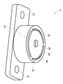
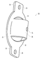
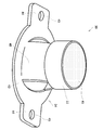
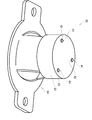
| TWI471971B (zh) * | 2007-10-30 | 2015-02-01 | 尼康股份有限公司 | Substrate holding member, substrate bonding apparatus, laminated substrate manufacturing apparatus, substrate bonding method, laminated substrate manufacturing method, and laminated semiconductor device manufacturing method |
-
2010
- 2010-07-20 TW TW099123776A patent/TW201131689A/zh unknown
- 2010-07-21 KR KR1020127004356A patent/KR20120037999A/ko not_active Ceased
- 2010-07-21 JP JP2011523552A patent/JP5810914B2/ja not_active Expired - Fee Related
- 2010-07-21 WO PCT/JP2010/004659 patent/WO2011010452A1/ja not_active Ceased
- 2010-07-21 IN IN1481DEN2012 patent/IN2012DN01481A/en unknown
- 2010-07-21 CN CN201080041652.XA patent/CN102498559B/zh not_active Expired - Fee Related
- 2010-07-21 EP EP10802073.6A patent/EP2458628A4/en not_active Withdrawn
-
2012
- 2012-01-20 US US13/354,570 patent/US9054140B2/en active Active
Cited By (4)
| Publication number | Priority date | Publication date | Assignee | Title |
|---|---|---|---|---|
| KR20150136482A (ko) * | 2013-03-27 | 2015-12-07 | 에베 그룹 에. 탈너 게엠베하 | 기판 스택을 취급하기 위한 장치 및 방법과 보유 장치 |
| KR20190093708A (ko) * | 2014-02-03 | 2019-08-09 | 에베 그룹 에. 탈너 게엠베하 | 기질을 결합하기 위한 방법 및 장치 |
| KR20200138415A (ko) * | 2014-02-03 | 2020-12-09 | 에베 그룹 에. 탈너 게엠베하 | 기질을 결합하기 위한 방법 및 장치 |
| KR20170096938A (ko) * | 2014-12-18 | 2017-08-25 | 에베 그룹 에. 탈너 게엠베하 | 기질을 접합시키기 위한 방법 |
Also Published As
| Publication number | Publication date |
|---|---|
| US20120205024A1 (en) | 2012-08-16 |
| TW201131689A (en) | 2011-09-16 |
| US9054140B2 (en) | 2015-06-09 |
| JPWO2011010452A1 (ja) | 2012-12-27 |
| IN2012DN01481A (https=) | 2015-06-05 |
| WO2011010452A1 (ja) | 2011-01-27 |
| CN102498559B (zh) | 2016-03-02 |
| EP2458628A1 (en) | 2012-05-30 |
| JP5810914B2 (ja) | 2015-11-11 |
| CN102498559A (zh) | 2012-06-13 |
| EP2458628A4 (en) | 2016-12-21 |
Similar Documents
| Publication | Publication Date | Title |
|---|---|---|
| KR20120037999A (ko) | 기판홀더 시스템, 기판접합장치 및 디바이스의 제조방법 | |
| US10714351B2 (en) | Multi-layered substrate manufacturing method | |
| KR101746241B1 (ko) | 기판처리 시스템, 기판홀더, 기판홀더쌍, 기판접합장치 및 디바이스의 제조방법 | |
| KR102637642B1 (ko) | 접합 방법, 접합 장치, 및 유지 부재 | |
| CN111566782B (zh) | 基板处理装置和基板处理方法 | |
| KR102012692B1 (ko) | 마이크로 소자 전사장치 및 마이크로 소자 전사방법 | |
| JP6742551B2 (ja) | 基板処理装置 | |
| JP2006339191A (ja) | ウェハホルダ、ウェハ積層方法及び積層型半導体装置製造方法 | |
| JPH09283392A (ja) | 基板の重ね合わせ方法及び装置 | |
| JP2010153645A (ja) | 積層半導体装置の製造方法 | |
| KR100715725B1 (ko) | 칩 실장장치 | |
| KR102781855B1 (ko) | 마그네틱 콜렛 | |
| JP5560590B2 (ja) | 基板貼り合わせ装置 | |
| EP1811828A1 (en) | Micromechanical placement system, and corresponding device | |
| JP2013026555A (ja) | 管理装置 |
Legal Events
| Date | Code | Title | Description |
|---|---|---|---|
| PA0105 | International application |
St.27 status event code: A-0-1-A10-A15-nap-PA0105 |
|
| P11-X000 | Amendment of application requested |
St.27 status event code: A-2-2-P10-P11-nap-X000 |
|
| P13-X000 | Application amended |
St.27 status event code: A-2-2-P10-P13-nap-X000 |
|
| PG1501 | Laying open of application |
St.27 status event code: A-1-1-Q10-Q12-nap-PG1501 |
|
| A201 | Request for examination | ||
| E13-X000 | Pre-grant limitation requested |
St.27 status event code: A-2-3-E10-E13-lim-X000 |
|
| P11-X000 | Amendment of application requested |
St.27 status event code: A-2-2-P10-P11-nap-X000 |
|
| P13-X000 | Application amended |
St.27 status event code: A-2-2-P10-P13-nap-X000 |
|
| PA0201 | Request for examination |
St.27 status event code: A-1-2-D10-D11-exm-PA0201 |
|
| R18-X000 | Changes to party contact information recorded |
St.27 status event code: A-3-3-R10-R18-oth-X000 |
|
| D13-X000 | Search requested |
St.27 status event code: A-1-2-D10-D13-srh-X000 |
|
| P22-X000 | Classification modified |
St.27 status event code: A-2-2-P10-P22-nap-X000 |
|
| D14-X000 | Search report completed |
St.27 status event code: A-1-2-D10-D14-srh-X000 |
|
| E902 | Notification of reason for refusal | ||
| PE0902 | Notice of grounds for rejection |
St.27 status event code: A-1-2-D10-D21-exm-PE0902 |
|
| E601 | Decision to refuse application | ||
| PE0601 | Decision on rejection of patent |
St.27 status event code: N-2-6-B10-B15-exm-PE0601 |
|
| R18-X000 | Changes to party contact information recorded |
St.27 status event code: A-3-3-R10-R18-oth-X000 |
|
| P22-X000 | Classification modified |
St.27 status event code: A-2-2-P10-P22-nap-X000 |