KR20120003390A - Semiconductor device - Google Patents
Semiconductor device Download PDFInfo
- Publication number
- KR20120003390A KR20120003390A KR1020110064841A KR20110064841A KR20120003390A KR 20120003390 A KR20120003390 A KR 20120003390A KR 1020110064841 A KR1020110064841 A KR 1020110064841A KR 20110064841 A KR20110064841 A KR 20110064841A KR 20120003390 A KR20120003390 A KR 20120003390A
- Authority
- KR
- South Korea
- Prior art keywords
- oxide
- oxide semiconductor
- insulating layer
- electrode
- film
- Prior art date
Links
- 239000004065 semiconductor Substances 0.000 title claims abstract description 281
- IJGRMHOSHXDMSA-UHFFFAOYSA-N Atomic nitrogen Chemical compound N#N IJGRMHOSHXDMSA-UHFFFAOYSA-N 0.000 claims abstract description 118
- 229910052757 nitrogen Inorganic materials 0.000 claims abstract description 60
- 229910052721 tungsten Inorganic materials 0.000 claims abstract description 28
- BASFCYQUMIYNBI-UHFFFAOYSA-N platinum Chemical compound [Pt] BASFCYQUMIYNBI-UHFFFAOYSA-N 0.000 claims abstract description 26
- WFKWXMTUELFFGS-UHFFFAOYSA-N tungsten Chemical compound [W] WFKWXMTUELFFGS-UHFFFAOYSA-N 0.000 claims abstract description 23
- 239000010937 tungsten Substances 0.000 claims abstract description 23
- 229910052750 molybdenum Inorganic materials 0.000 claims abstract description 14
- 229910052697 platinum Inorganic materials 0.000 claims abstract description 12
- ZOKXTWBITQBERF-UHFFFAOYSA-N Molybdenum Chemical compound [Mo] ZOKXTWBITQBERF-UHFFFAOYSA-N 0.000 claims abstract description 10
- 239000011733 molybdenum Substances 0.000 claims abstract description 10
- 229910052760 oxygen Inorganic materials 0.000 claims description 126
- QVGXLLKOCUKJST-UHFFFAOYSA-N atomic oxygen Chemical compound [O] QVGXLLKOCUKJST-UHFFFAOYSA-N 0.000 claims description 125
- 239000001301 oxygen Substances 0.000 claims description 125
- 238000000034 method Methods 0.000 claims description 86
- 229910001195 gallium oxide Inorganic materials 0.000 claims description 28
- 239000000203 mixture Substances 0.000 claims description 24
- 229910052733 gallium Inorganic materials 0.000 claims description 22
- TWNQGVIAIRXVLR-UHFFFAOYSA-N oxo(oxoalumanyloxy)alumane Chemical compound O=[Al]O[Al]=O TWNQGVIAIRXVLR-UHFFFAOYSA-N 0.000 claims description 21
- AJNVQOSZGJRYEI-UHFFFAOYSA-N digallium;oxygen(2-) Chemical compound [O-2].[O-2].[O-2].[Ga+3].[Ga+3] AJNVQOSZGJRYEI-UHFFFAOYSA-N 0.000 claims description 16
- GYHNNYVSQQEPJS-UHFFFAOYSA-N Gallium Chemical compound [Ga] GYHNNYVSQQEPJS-UHFFFAOYSA-N 0.000 claims description 14
- 229910044991 metal oxide Inorganic materials 0.000 claims description 13
- 150000004706 metal oxides Chemical group 0.000 claims description 13
- RNQKDQAVIXDKAG-UHFFFAOYSA-N aluminum gallium Chemical compound [Al].[Ga] RNQKDQAVIXDKAG-UHFFFAOYSA-N 0.000 claims description 12
- 229910052795 boron group element Inorganic materials 0.000 claims description 7
- 229910052751 metal Inorganic materials 0.000 abstract description 20
- 239000002184 metal Substances 0.000 abstract description 19
- 238000009413 insulation Methods 0.000 abstract description 6
- 239000003963 antioxidant agent Substances 0.000 abstract 1
- 230000003078 antioxidant effect Effects 0.000 abstract 1
- 235000006708 antioxidants Nutrition 0.000 abstract 1
- 239000010410 layer Substances 0.000 description 265
- 239000010408 film Substances 0.000 description 174
- 239000000758 substrate Substances 0.000 description 69
- 239000004973 liquid crystal related substance Substances 0.000 description 38
- 239000000463 material Substances 0.000 description 38
- 230000008569 process Effects 0.000 description 33
- 238000010438 heat treatment Methods 0.000 description 29
- 239000001257 hydrogen Substances 0.000 description 29
- 229910052739 hydrogen Inorganic materials 0.000 description 29
- XLYOFNOQVPJJNP-UHFFFAOYSA-N water Substances O XLYOFNOQVPJJNP-UHFFFAOYSA-N 0.000 description 28
- 229910001868 water Inorganic materials 0.000 description 28
- XKRFYHLGVUSROY-UHFFFAOYSA-N Argon Chemical compound [Ar] XKRFYHLGVUSROY-UHFFFAOYSA-N 0.000 description 26
- 238000004544 sputter deposition Methods 0.000 description 25
- 229910007541 Zn O Inorganic materials 0.000 description 22
- 125000004429 atom Chemical group 0.000 description 21
- 239000012298 atmosphere Substances 0.000 description 20
- 239000012535 impurity Substances 0.000 description 20
- 239000013078 crystal Substances 0.000 description 19
- 239000007789 gas Substances 0.000 description 18
- 230000006870 function Effects 0.000 description 17
- UFHFLCQGNIYNRP-UHFFFAOYSA-N Hydrogen Chemical compound [H][H] UFHFLCQGNIYNRP-UHFFFAOYSA-N 0.000 description 16
- XLOMVQKBTHCTTD-UHFFFAOYSA-N Zinc monoxide Chemical compound [Zn]=O XLOMVQKBTHCTTD-UHFFFAOYSA-N 0.000 description 16
- 230000015572 biosynthetic process Effects 0.000 description 16
- 239000002245 particle Substances 0.000 description 15
- 239000011521 glass Substances 0.000 description 14
- 238000012360 testing method Methods 0.000 description 14
- 229910052786 argon Inorganic materials 0.000 description 13
- 238000005401 electroluminescence Methods 0.000 description 13
- 150000002431 hydrogen Chemical class 0.000 description 13
- 230000008859 change Effects 0.000 description 12
- 230000003287 optical effect Effects 0.000 description 12
- 238000004519 manufacturing process Methods 0.000 description 11
- 239000010936 titanium Substances 0.000 description 10
- 229910052782 aluminium Inorganic materials 0.000 description 9
- 230000007547 defect Effects 0.000 description 9
- 238000005530 etching Methods 0.000 description 9
- 238000005259 measurement Methods 0.000 description 9
- 239000010409 thin film Substances 0.000 description 9
- 239000000123 paper Substances 0.000 description 8
- 238000000206 photolithography Methods 0.000 description 8
- 229920005989 resin Polymers 0.000 description 8
- 239000011347 resin Substances 0.000 description 8
- 239000011701 zinc Substances 0.000 description 8
- 239000011787 zinc oxide Substances 0.000 description 8
- 229910052581 Si3N4 Inorganic materials 0.000 description 7
- XAGFODPZIPBFFR-UHFFFAOYSA-N aluminium Chemical compound [Al] XAGFODPZIPBFFR-UHFFFAOYSA-N 0.000 description 7
- 229910052738 indium Inorganic materials 0.000 description 7
- HQVNEWCFYHHQES-UHFFFAOYSA-N silicon nitride Chemical compound N12[Si]34N5[Si]62N3[Si]51N64 HQVNEWCFYHHQES-UHFFFAOYSA-N 0.000 description 7
- 239000012798 spherical particle Substances 0.000 description 7
- XUIMIQQOPSSXEZ-UHFFFAOYSA-N Silicon Chemical compound [Si] XUIMIQQOPSSXEZ-UHFFFAOYSA-N 0.000 description 6
- 239000000945 filler Substances 0.000 description 6
- 239000011261 inert gas Substances 0.000 description 6
- 239000011810 insulating material Substances 0.000 description 6
- 238000001004 secondary ion mass spectrometry Methods 0.000 description 6
- 229910052710 silicon Inorganic materials 0.000 description 6
- 239000010703 silicon Substances 0.000 description 6
- 238000004364 calculation method Methods 0.000 description 5
- 230000000694 effects Effects 0.000 description 5
- 125000002887 hydroxy group Chemical group [H]O* 0.000 description 5
- 239000003094 microcapsule Substances 0.000 description 5
- 230000001681 protective effect Effects 0.000 description 5
- 239000003566 sealing material Substances 0.000 description 5
- 229910052719 titanium Inorganic materials 0.000 description 5
- 229910005191 Ga 2 O 3 Inorganic materials 0.000 description 4
- 206010021143 Hypoxia Diseases 0.000 description 4
- RTAQQCXQSZGOHL-UHFFFAOYSA-N Titanium Chemical compound [Ti] RTAQQCXQSZGOHL-UHFFFAOYSA-N 0.000 description 4
- 238000004458 analytical method Methods 0.000 description 4
- 239000011651 chromium Substances 0.000 description 4
- 229920001940 conductive polymer Polymers 0.000 description 4
- 230000018044 dehydration Effects 0.000 description 4
- 238000006297 dehydration reaction Methods 0.000 description 4
- 238000006356 dehydrogenation reaction Methods 0.000 description 4
- 238000010586 diagram Methods 0.000 description 4
- 230000005684 electric field Effects 0.000 description 4
- 239000011229 interlayer Substances 0.000 description 4
- 239000012528 membrane Substances 0.000 description 4
- 239000012299 nitrogen atmosphere Substances 0.000 description 4
- 239000002356 single layer Substances 0.000 description 4
- 239000004925 Acrylic resin Substances 0.000 description 3
- 229920000178 Acrylic resin Polymers 0.000 description 3
- 229910019092 Mg-O Inorganic materials 0.000 description 3
- 229910019395 Mg—O Inorganic materials 0.000 description 3
- 239000004642 Polyimide Substances 0.000 description 3
- VYPSYNLAJGMNEJ-UHFFFAOYSA-N Silicium dioxide Chemical compound O=[Si]=O VYPSYNLAJGMNEJ-UHFFFAOYSA-N 0.000 description 3
- GWEVSGVZZGPLCZ-UHFFFAOYSA-N Titan oxide Chemical compound O=[Ti]=O GWEVSGVZZGPLCZ-UHFFFAOYSA-N 0.000 description 3
- 229910052804 chromium Inorganic materials 0.000 description 3
- 238000004891 communication Methods 0.000 description 3
- 239000005262 ferroelectric liquid crystals (FLCs) Substances 0.000 description 3
- 239000010931 gold Substances 0.000 description 3
- 229910052734 helium Inorganic materials 0.000 description 3
- 239000001307 helium Substances 0.000 description 3
- SWQJXJOGLNCZEY-UHFFFAOYSA-N helium atom Chemical compound [He] SWQJXJOGLNCZEY-UHFFFAOYSA-N 0.000 description 3
- 150000004678 hydrides Chemical class 0.000 description 3
- 238000010348 incorporation Methods 0.000 description 3
- APFVFJFRJDLVQX-UHFFFAOYSA-N indium atom Chemical compound [In] APFVFJFRJDLVQX-UHFFFAOYSA-N 0.000 description 3
- 230000007246 mechanism Effects 0.000 description 3
- 150000002894 organic compounds Chemical class 0.000 description 3
- 238000005192 partition Methods 0.000 description 3
- 238000009832 plasma treatment Methods 0.000 description 3
- 229920003023 plastic Polymers 0.000 description 3
- 239000004033 plastic Substances 0.000 description 3
- 229920001721 polyimide Polymers 0.000 description 3
- 229920002620 polyvinyl fluoride Polymers 0.000 description 3
- 238000012545 processing Methods 0.000 description 3
- 229910052814 silicon oxide Inorganic materials 0.000 description 3
- 239000000126 substance Substances 0.000 description 3
- JBQYATWDVHIOAR-UHFFFAOYSA-N tellanylidenegermanium Chemical compound [Te]=[Ge] JBQYATWDVHIOAR-UHFFFAOYSA-N 0.000 description 3
- OGIDPMRJRNCKJF-UHFFFAOYSA-N titanium oxide Inorganic materials [Ti]=O OGIDPMRJRNCKJF-UHFFFAOYSA-N 0.000 description 3
- 229910052724 xenon Inorganic materials 0.000 description 3
- FHNFHKCVQCLJFQ-UHFFFAOYSA-N xenon atom Chemical compound [Xe] FHNFHKCVQCLJFQ-UHFFFAOYSA-N 0.000 description 3
- PAYRUJLWNCNPSJ-UHFFFAOYSA-N Aniline Chemical compound NC1=CC=CC=C1 PAYRUJLWNCNPSJ-UHFFFAOYSA-N 0.000 description 2
- CURLTUGMZLYLDI-UHFFFAOYSA-N Carbon dioxide Chemical compound O=C=O CURLTUGMZLYLDI-UHFFFAOYSA-N 0.000 description 2
- VYZAMTAEIAYCRO-UHFFFAOYSA-N Chromium Chemical compound [Cr] VYZAMTAEIAYCRO-UHFFFAOYSA-N 0.000 description 2
- RYGMFSIKBFXOCR-UHFFFAOYSA-N Copper Chemical compound [Cu] RYGMFSIKBFXOCR-UHFFFAOYSA-N 0.000 description 2
- 206010052128 Glare Diseases 0.000 description 2
- PXHVJJICTQNCMI-UHFFFAOYSA-N Nickel Chemical compound [Ni] PXHVJJICTQNCMI-UHFFFAOYSA-N 0.000 description 2
- OAICVXFJPJFONN-UHFFFAOYSA-N Phosphorus Chemical compound [P] OAICVXFJPJFONN-UHFFFAOYSA-N 0.000 description 2
- 239000004952 Polyamide Substances 0.000 description 2
- KAESVJOAVNADME-UHFFFAOYSA-N Pyrrole Chemical compound C=1C=CNC=1 KAESVJOAVNADME-UHFFFAOYSA-N 0.000 description 2
- YTPLMLYBLZKORZ-UHFFFAOYSA-N Thiophene Chemical compound C=1C=CSC=1 YTPLMLYBLZKORZ-UHFFFAOYSA-N 0.000 description 2
- GDFCWFBWQUEQIJ-UHFFFAOYSA-N [B].[P] Chemical compound [B].[P] GDFCWFBWQUEQIJ-UHFFFAOYSA-N 0.000 description 2
- 239000000956 alloy Substances 0.000 description 2
- UMIVXZPTRXBADB-UHFFFAOYSA-N benzocyclobutene Chemical compound C1=CC=C2CCC2=C1 UMIVXZPTRXBADB-UHFFFAOYSA-N 0.000 description 2
- 230000005540 biological transmission Effects 0.000 description 2
- 239000005380 borophosphosilicate glass Substances 0.000 description 2
- DQXBYHZEEUGOBF-UHFFFAOYSA-N but-3-enoic acid;ethene Chemical compound C=C.OC(=O)CC=C DQXBYHZEEUGOBF-UHFFFAOYSA-N 0.000 description 2
- 239000003990 capacitor Substances 0.000 description 2
- 229910052799 carbon Inorganic materials 0.000 description 2
- 239000000969 carrier Substances 0.000 description 2
- 230000003098 cholesteric effect Effects 0.000 description 2
- 239000011248 coating agent Substances 0.000 description 2
- 238000000576 coating method Methods 0.000 description 2
- 239000003086 colorant Substances 0.000 description 2
- 150000001875 compounds Chemical class 0.000 description 2
- 239000004020 conductor Substances 0.000 description 2
- 229910052802 copper Inorganic materials 0.000 description 2
- 239000010949 copper Substances 0.000 description 2
- 238000000151 deposition Methods 0.000 description 2
- KPUWHANPEXNPJT-UHFFFAOYSA-N disiloxane Chemical class [SiH3]O[SiH3] KPUWHANPEXNPJT-UHFFFAOYSA-N 0.000 description 2
- 239000003822 epoxy resin Substances 0.000 description 2
- 239000005038 ethylene vinyl acetate Substances 0.000 description 2
- 230000005281 excited state Effects 0.000 description 2
- 238000000605 extraction Methods 0.000 description 2
- 239000011152 fibreglass Substances 0.000 description 2
- 238000011049 filling Methods 0.000 description 2
- 238000007667 floating Methods 0.000 description 2
- 229910052737 gold Inorganic materials 0.000 description 2
- 229910052735 hafnium Inorganic materials 0.000 description 2
- VBJZVLUMGGDVMO-UHFFFAOYSA-N hafnium atom Chemical compound [Hf] VBJZVLUMGGDVMO-UHFFFAOYSA-N 0.000 description 2
- 125000004435 hydrogen atom Chemical group [H]* 0.000 description 2
- 150000002483 hydrogen compounds Chemical class 0.000 description 2
- 229910003437 indium oxide Inorganic materials 0.000 description 2
- PJXISJQVUVHSOJ-UHFFFAOYSA-N indium(iii) oxide Chemical compound [O-2].[O-2].[O-2].[In+3].[In+3] PJXISJQVUVHSOJ-UHFFFAOYSA-N 0.000 description 2
- AMGQUBHHOARCQH-UHFFFAOYSA-N indium;oxotin Chemical compound [In].[Sn]=O AMGQUBHHOARCQH-UHFFFAOYSA-N 0.000 description 2
- 238000002347 injection Methods 0.000 description 2
- 239000007924 injection Substances 0.000 description 2
- 238000003475 lamination Methods 0.000 description 2
- 239000007788 liquid Substances 0.000 description 2
- 229910052748 manganese Inorganic materials 0.000 description 2
- 239000011159 matrix material Substances 0.000 description 2
- 229910052754 neon Inorganic materials 0.000 description 2
- GKAOGPIIYCISHV-UHFFFAOYSA-N neon atom Chemical compound [Ne] GKAOGPIIYCISHV-UHFFFAOYSA-N 0.000 description 2
- QGLKJKCYBOYXKC-UHFFFAOYSA-N nonaoxidotritungsten Chemical compound O=[W]1(=O)O[W](=O)(=O)O[W](=O)(=O)O1 QGLKJKCYBOYXKC-UHFFFAOYSA-N 0.000 description 2
- 239000011368 organic material Substances 0.000 description 2
- 229910052698 phosphorus Inorganic materials 0.000 description 2
- 239000011574 phosphorus Substances 0.000 description 2
- 238000005268 plasma chemical vapour deposition Methods 0.000 description 2
- 229920001200 poly(ethylene-vinyl acetate) Polymers 0.000 description 2
- 229920002037 poly(vinyl butyral) polymer Polymers 0.000 description 2
- 229920002647 polyamide Polymers 0.000 description 2
- 229920000647 polyepoxide Polymers 0.000 description 2
- 229920006267 polyester film Polymers 0.000 description 2
- 229920000915 polyvinyl chloride Polymers 0.000 description 2
- 239000004800 polyvinyl chloride Substances 0.000 description 2
- 230000005855 radiation Effects 0.000 description 2
- -1 silicon Chemical compound 0.000 description 2
- 239000002904 solvent Substances 0.000 description 2
- 125000006850 spacer group Chemical group 0.000 description 2
- 238000003860 storage Methods 0.000 description 2
- 229910052715 tantalum Inorganic materials 0.000 description 2
- GUVRBAGPIYLISA-UHFFFAOYSA-N tantalum atom Chemical compound [Ta] GUVRBAGPIYLISA-UHFFFAOYSA-N 0.000 description 2
- 230000007704 transition Effects 0.000 description 2
- 229910001930 tungsten oxide Inorganic materials 0.000 description 2
- 229910052725 zinc Inorganic materials 0.000 description 2
- YVTHLONGBIQYBO-UHFFFAOYSA-N zinc indium(3+) oxygen(2-) Chemical compound [O--].[Zn++].[In+3] YVTHLONGBIQYBO-UHFFFAOYSA-N 0.000 description 2
- UWCWUCKPEYNDNV-LBPRGKRZSA-N 2,6-dimethyl-n-[[(2s)-pyrrolidin-2-yl]methyl]aniline Chemical compound CC1=CC=CC(C)=C1NC[C@H]1NCCC1 UWCWUCKPEYNDNV-LBPRGKRZSA-N 0.000 description 1
- OKTJSMMVPCPJKN-UHFFFAOYSA-N Carbon Chemical compound [C] OKTJSMMVPCPJKN-UHFFFAOYSA-N 0.000 description 1
- 239000004986 Cholesteric liquid crystals (ChLC) Substances 0.000 description 1
- 108091006149 Electron carriers Proteins 0.000 description 1
- 239000004593 Epoxy Substances 0.000 description 1
- 229910002601 GaN Inorganic materials 0.000 description 1
- JMASRVWKEDWRBT-UHFFFAOYSA-N Gallium nitride Chemical compound [Ga]#N JMASRVWKEDWRBT-UHFFFAOYSA-N 0.000 description 1
- 239000005264 High molar mass liquid crystal Substances 0.000 description 1
- DGAQECJNVWCQMB-PUAWFVPOSA-M Ilexoside XXIX Chemical compound C[C@@H]1CC[C@@]2(CC[C@@]3(C(=CC[C@H]4[C@]3(CC[C@@H]5[C@@]4(CC[C@@H](C5(C)C)OS(=O)(=O)[O-])C)C)[C@@H]2[C@]1(C)O)C)C(=O)O[C@H]6[C@@H]([C@H]([C@@H]([C@H](O6)CO)O)O)O.[Na+] DGAQECJNVWCQMB-PUAWFVPOSA-M 0.000 description 1
- 108010083687 Ion Pumps Proteins 0.000 description 1
- 229910052779 Neodymium Inorganic materials 0.000 description 1
- 241000589614 Pseudomonas stutzeri Species 0.000 description 1
- 229910004298 SiO 2 Inorganic materials 0.000 description 1
- BQCADISMDOOEFD-UHFFFAOYSA-N Silver Chemical compound [Ag] BQCADISMDOOEFD-UHFFFAOYSA-N 0.000 description 1
- 239000004990 Smectic liquid crystal Substances 0.000 description 1
- 229910020923 Sn-O Inorganic materials 0.000 description 1
- 239000004974 Thermotropic liquid crystal Substances 0.000 description 1
- QCWXUUIWCKQGHC-UHFFFAOYSA-N Zirconium Chemical compound [Zr] QCWXUUIWCKQGHC-UHFFFAOYSA-N 0.000 description 1
- NIXOWILDQLNWCW-UHFFFAOYSA-N acrylic acid group Chemical group C(C=C)(=O)O NIXOWILDQLNWCW-UHFFFAOYSA-N 0.000 description 1
- 230000009471 action Effects 0.000 description 1
- 229910045601 alloy Inorganic materials 0.000 description 1
- 230000003667 anti-reflective effect Effects 0.000 description 1
- NWAIGJYBQQYSPW-UHFFFAOYSA-N azanylidyneindigane Chemical compound [In]#N NWAIGJYBQQYSPW-UHFFFAOYSA-N 0.000 description 1
- 230000004888 barrier function Effects 0.000 description 1
- 230000008901 benefit Effects 0.000 description 1
- 239000011230 binding agent Substances 0.000 description 1
- 150000001721 carbon Chemical group 0.000 description 1
- 229910002092 carbon dioxide Inorganic materials 0.000 description 1
- 239000001569 carbon dioxide Substances 0.000 description 1
- 229910052800 carbon group element Inorganic materials 0.000 description 1
- 239000003795 chemical substances by application Substances 0.000 description 1
- 229910017052 cobalt Inorganic materials 0.000 description 1
- 239000010941 cobalt Substances 0.000 description 1
- GUTLYIVDDKVIGB-UHFFFAOYSA-N cobalt atom Chemical compound [Co] GUTLYIVDDKVIGB-UHFFFAOYSA-N 0.000 description 1
- 239000002131 composite material Substances 0.000 description 1
- 239000000470 constituent Substances 0.000 description 1
- 229920001577 copolymer Polymers 0.000 description 1
- PMHQVHHXPFUNSP-UHFFFAOYSA-M copper(1+);methylsulfanylmethane;bromide Chemical compound Br[Cu].CSC PMHQVHHXPFUNSP-UHFFFAOYSA-M 0.000 description 1
- 238000007766 curtain coating Methods 0.000 description 1
- 238000005520 cutting process Methods 0.000 description 1
- 230000007423 decrease Effects 0.000 description 1
- 238000007872 degassing Methods 0.000 description 1
- 230000008021 deposition Effects 0.000 description 1
- 238000013461 design Methods 0.000 description 1
- 230000006866 deterioration Effects 0.000 description 1
- 238000011161 development Methods 0.000 description 1
- 238000009792 diffusion process Methods 0.000 description 1
- 238000007598 dipping method Methods 0.000 description 1
- 239000006185 dispersion Substances 0.000 description 1
- 239000004815 dispersion polymer Substances 0.000 description 1
- 238000009826 distribution Methods 0.000 description 1
- 238000001312 dry etching Methods 0.000 description 1
- 239000000428 dust Substances 0.000 description 1
- 230000005611 electricity Effects 0.000 description 1
- 238000011156 evaluation Methods 0.000 description 1
- 230000005284 excitation Effects 0.000 description 1
- 230000007717 exclusion Effects 0.000 description 1
- 239000004744 fabric Substances 0.000 description 1
- 230000005669 field effect Effects 0.000 description 1
- 239000011888 foil Substances 0.000 description 1
- 238000003197 gene knockdown Methods 0.000 description 1
- 230000004313 glare Effects 0.000 description 1
- PCHJSUWPFVWCPO-UHFFFAOYSA-N gold Chemical compound [Au] PCHJSUWPFVWCPO-UHFFFAOYSA-N 0.000 description 1
- 230000005283 ground state Effects 0.000 description 1
- 229910021480 group 4 element Inorganic materials 0.000 description 1
- 229910000449 hafnium oxide Inorganic materials 0.000 description 1
- WIHZLLGSGQNAGK-UHFFFAOYSA-N hafnium(4+);oxygen(2-) Chemical compound [O-2].[O-2].[Hf+4] WIHZLLGSGQNAGK-UHFFFAOYSA-N 0.000 description 1
- 229910052736 halogen Inorganic materials 0.000 description 1
- 150000002367 halogens Chemical class 0.000 description 1
- 238000005286 illumination Methods 0.000 description 1
- RHZWSUVWRRXEJF-UHFFFAOYSA-N indium tin Chemical compound [In].[Sn] RHZWSUVWRRXEJF-UHFFFAOYSA-N 0.000 description 1
- 150000002484 inorganic compounds Chemical class 0.000 description 1
- 229910010272 inorganic material Inorganic materials 0.000 description 1
- 238000003780 insertion Methods 0.000 description 1
- 230000037431 insertion Effects 0.000 description 1
- 239000012212 insulator Substances 0.000 description 1
- 238000009830 intercalation Methods 0.000 description 1
- 230000002687 intercalation Effects 0.000 description 1
- 230000002452 interceptive effect Effects 0.000 description 1
- 238000010030 laminating Methods 0.000 description 1
- 239000000696 magnetic material Substances 0.000 description 1
- 230000014759 maintenance of location Effects 0.000 description 1
- QSHDDOUJBYECFT-UHFFFAOYSA-N mercury Chemical compound [Hg] QSHDDOUJBYECFT-UHFFFAOYSA-N 0.000 description 1
- 229910052753 mercury Inorganic materials 0.000 description 1
- 229910001507 metal halide Inorganic materials 0.000 description 1
- 150000005309 metal halides Chemical class 0.000 description 1
- 229910021645 metal ion Inorganic materials 0.000 description 1
- 239000007769 metal material Substances 0.000 description 1
- 150000002739 metals Chemical class 0.000 description 1
- 229910000476 molybdenum oxide Inorganic materials 0.000 description 1
- QEFYFXOXNSNQGX-UHFFFAOYSA-N neodymium atom Chemical compound [Nd] QEFYFXOXNSNQGX-UHFFFAOYSA-N 0.000 description 1
- 229910052759 nickel Inorganic materials 0.000 description 1
- 229910052758 niobium Inorganic materials 0.000 description 1
- 239000010955 niobium Substances 0.000 description 1
- GUCVJGMIXFAOAE-UHFFFAOYSA-N niobium atom Chemical compound [Nb] GUCVJGMIXFAOAE-UHFFFAOYSA-N 0.000 description 1
- 150000004767 nitrides Chemical class 0.000 description 1
- 238000007645 offset printing Methods 0.000 description 1
- 239000012788 optical film Substances 0.000 description 1
- PQQKPALAQIIWST-UHFFFAOYSA-N oxomolybdenum Chemical compound [Mo]=O PQQKPALAQIIWST-UHFFFAOYSA-N 0.000 description 1
- DOVLZBWRSUUIJA-UHFFFAOYSA-N oxotin;silicon Chemical compound [Si].[Sn]=O DOVLZBWRSUUIJA-UHFFFAOYSA-N 0.000 description 1
- 230000003071 parasitic effect Effects 0.000 description 1
- 230000035515 penetration Effects 0.000 description 1
- 239000012466 permeate Substances 0.000 description 1
- 239000000049 pigment Substances 0.000 description 1
- 230000010287 polarization Effects 0.000 description 1
- 229920000767 polyaniline Polymers 0.000 description 1
- 229920000128 polypyrrole Polymers 0.000 description 1
- 229920000123 polythiophene Polymers 0.000 description 1
- 230000000750 progressive effect Effects 0.000 description 1
- 238000004151 rapid thermal annealing Methods 0.000 description 1
- 230000006798 recombination Effects 0.000 description 1
- 238000005215 recombination Methods 0.000 description 1
- 238000002310 reflectometry Methods 0.000 description 1
- 230000004044 response Effects 0.000 description 1
- 229910052706 scandium Inorganic materials 0.000 description 1
- SIXSYDAISGFNSX-UHFFFAOYSA-N scandium atom Chemical compound [Sc] SIXSYDAISGFNSX-UHFFFAOYSA-N 0.000 description 1
- 238000007650 screen-printing Methods 0.000 description 1
- 238000007789 sealing Methods 0.000 description 1
- 229920002050 silicone resin Polymers 0.000 description 1
- 229910052709 silver Inorganic materials 0.000 description 1
- 239000004332 silver Substances 0.000 description 1
- 229910052708 sodium Inorganic materials 0.000 description 1
- 239000011734 sodium Substances 0.000 description 1
- 238000001179 sorption measurement Methods 0.000 description 1
- 238000001228 spectrum Methods 0.000 description 1
- 238000004528 spin coating Methods 0.000 description 1
- 238000005507 spraying Methods 0.000 description 1
- 230000003068 static effect Effects 0.000 description 1
- 238000000859 sublimation Methods 0.000 description 1
- 230000008022 sublimation Effects 0.000 description 1
- 238000010345 tape casting Methods 0.000 description 1
- 229920001187 thermosetting polymer Polymers 0.000 description 1
- 229930192474 thiophene Natural products 0.000 description 1
- 238000002834 transmittance Methods 0.000 description 1
- 229910052720 vanadium Inorganic materials 0.000 description 1
- GPPXJZIENCGNKB-UHFFFAOYSA-N vanadium Chemical compound [V]#[V] GPPXJZIENCGNKB-UHFFFAOYSA-N 0.000 description 1
- 238000001039 wet etching Methods 0.000 description 1
- 229910052727 yttrium Inorganic materials 0.000 description 1
- VWQVUPCCIRVNHF-UHFFFAOYSA-N yttrium atom Chemical compound [Y] VWQVUPCCIRVNHF-UHFFFAOYSA-N 0.000 description 1
- 229910052726 zirconium Inorganic materials 0.000 description 1
Images


Classifications
-
- H—ELECTRICITY
- H01—ELECTRIC ELEMENTS
- H01L—SEMICONDUCTOR DEVICES NOT COVERED BY CLASS H10
- H01L29/00—Semiconductor devices adapted for rectifying, amplifying, oscillating or switching, or capacitors or resistors with at least one potential-jump barrier or surface barrier, e.g. PN junction depletion layer or carrier concentration layer; Details of semiconductor bodies or of electrodes thereof ; Multistep manufacturing processes therefor
- H01L29/66—Types of semiconductor device ; Multistep manufacturing processes therefor
- H01L29/68—Types of semiconductor device ; Multistep manufacturing processes therefor controllable by only the electric current supplied, or only the electric potential applied, to an electrode which does not carry the current to be rectified, amplified or switched
- H01L29/76—Unipolar devices, e.g. field effect transistors
- H01L29/772—Field effect transistors
- H01L29/78—Field effect transistors with field effect produced by an insulated gate
- H01L29/786—Thin film transistors, i.e. transistors with a channel being at least partly a thin film
- H01L29/7869—Thin film transistors, i.e. transistors with a channel being at least partly a thin film having a semiconductor body comprising an oxide semiconductor material, e.g. zinc oxide, copper aluminium oxide, cadmium stannate
-
- H—ELECTRICITY
- H01—ELECTRIC ELEMENTS
- H01L—SEMICONDUCTOR DEVICES NOT COVERED BY CLASS H10
- H01L29/00—Semiconductor devices adapted for rectifying, amplifying, oscillating or switching, or capacitors or resistors with at least one potential-jump barrier or surface barrier, e.g. PN junction depletion layer or carrier concentration layer; Details of semiconductor bodies or of electrodes thereof ; Multistep manufacturing processes therefor
- H01L29/40—Electrodes ; Multistep manufacturing processes therefor
- H01L29/43—Electrodes ; Multistep manufacturing processes therefor characterised by the materials of which they are formed
- H01L29/45—Ohmic electrodes
-
- H—ELECTRICITY
- H01—ELECTRIC ELEMENTS
- H01L—SEMICONDUCTOR DEVICES NOT COVERED BY CLASS H10
- H01L29/00—Semiconductor devices adapted for rectifying, amplifying, oscillating or switching, or capacitors or resistors with at least one potential-jump barrier or surface barrier, e.g. PN junction depletion layer or carrier concentration layer; Details of semiconductor bodies or of electrodes thereof ; Multistep manufacturing processes therefor
- H01L29/40—Electrodes ; Multistep manufacturing processes therefor
- H01L29/43—Electrodes ; Multistep manufacturing processes therefor characterised by the materials of which they are formed
- H01L29/49—Metal-insulator-semiconductor electrodes, e.g. gates of MOSFET
- H01L29/4908—Metal-insulator-semiconductor electrodes, e.g. gates of MOSFET for thin film semiconductor, e.g. gate of TFT
-
- H—ELECTRICITY
- H01—ELECTRIC ELEMENTS
- H01L—SEMICONDUCTOR DEVICES NOT COVERED BY CLASS H10
- H01L29/00—Semiconductor devices adapted for rectifying, amplifying, oscillating or switching, or capacitors or resistors with at least one potential-jump barrier or surface barrier, e.g. PN junction depletion layer or carrier concentration layer; Details of semiconductor bodies or of electrodes thereof ; Multistep manufacturing processes therefor
- H01L29/40—Electrodes ; Multistep manufacturing processes therefor
- H01L29/43—Electrodes ; Multistep manufacturing processes therefor characterised by the materials of which they are formed
- H01L29/49—Metal-insulator-semiconductor electrodes, e.g. gates of MOSFET
- H01L29/51—Insulating materials associated therewith
- H01L29/517—Insulating materials associated therewith the insulating material comprising a metallic compound, e.g. metal oxide, metal silicate
-
- H—ELECTRICITY
- H01—ELECTRIC ELEMENTS
- H01L—SEMICONDUCTOR DEVICES NOT COVERED BY CLASS H10
- H01L29/00—Semiconductor devices adapted for rectifying, amplifying, oscillating or switching, or capacitors or resistors with at least one potential-jump barrier or surface barrier, e.g. PN junction depletion layer or carrier concentration layer; Details of semiconductor bodies or of electrodes thereof ; Multistep manufacturing processes therefor
- H01L29/66—Types of semiconductor device ; Multistep manufacturing processes therefor
- H01L29/68—Types of semiconductor device ; Multistep manufacturing processes therefor controllable by only the electric current supplied, or only the electric potential applied, to an electrode which does not carry the current to be rectified, amplified or switched
- H01L29/76—Unipolar devices, e.g. field effect transistors
- H01L29/772—Field effect transistors
- H01L29/78—Field effect transistors with field effect produced by an insulated gate
- H01L29/786—Thin film transistors, i.e. transistors with a channel being at least partly a thin film
- H01L29/78606—Thin film transistors, i.e. transistors with a channel being at least partly a thin film with supplementary region or layer in the thin film or in the insulated bulk substrate supporting it for controlling or increasing the safety of the device
-
- H—ELECTRICITY
- H01—ELECTRIC ELEMENTS
- H01L—SEMICONDUCTOR DEVICES NOT COVERED BY CLASS H10
- H01L29/00—Semiconductor devices adapted for rectifying, amplifying, oscillating or switching, or capacitors or resistors with at least one potential-jump barrier or surface barrier, e.g. PN junction depletion layer or carrier concentration layer; Details of semiconductor bodies or of electrodes thereof ; Multistep manufacturing processes therefor
- H01L29/66—Types of semiconductor device ; Multistep manufacturing processes therefor
- H01L29/68—Types of semiconductor device ; Multistep manufacturing processes therefor controllable by only the electric current supplied, or only the electric potential applied, to an electrode which does not carry the current to be rectified, amplified or switched
- H01L29/76—Unipolar devices, e.g. field effect transistors
- H01L29/772—Field effect transistors
- H01L29/78—Field effect transistors with field effect produced by an insulated gate
- H01L29/786—Thin film transistors, i.e. transistors with a channel being at least partly a thin film
- H01L29/78645—Thin film transistors, i.e. transistors with a channel being at least partly a thin film with multiple gate
- H01L29/78648—Thin film transistors, i.e. transistors with a channel being at least partly a thin film with multiple gate arranged on opposing sides of the channel
-
- H—ELECTRICITY
- H01—ELECTRIC ELEMENTS
- H01L—SEMICONDUCTOR DEVICES NOT COVERED BY CLASS H10
- H01L29/00—Semiconductor devices adapted for rectifying, amplifying, oscillating or switching, or capacitors or resistors with at least one potential-jump barrier or surface barrier, e.g. PN junction depletion layer or carrier concentration layer; Details of semiconductor bodies or of electrodes thereof ; Multistep manufacturing processes therefor
- H01L29/66—Types of semiconductor device ; Multistep manufacturing processes therefor
- H01L29/68—Types of semiconductor device ; Multistep manufacturing processes therefor controllable by only the electric current supplied, or only the electric potential applied, to an electrode which does not carry the current to be rectified, amplified or switched
- H01L29/76—Unipolar devices, e.g. field effect transistors
- H01L29/772—Field effect transistors
- H01L29/78—Field effect transistors with field effect produced by an insulated gate
- H01L29/786—Thin film transistors, i.e. transistors with a channel being at least partly a thin film
- H01L29/7869—Thin film transistors, i.e. transistors with a channel being at least partly a thin film having a semiconductor body comprising an oxide semiconductor material, e.g. zinc oxide, copper aluminium oxide, cadmium stannate
- H01L29/78693—Thin film transistors, i.e. transistors with a channel being at least partly a thin film having a semiconductor body comprising an oxide semiconductor material, e.g. zinc oxide, copper aluminium oxide, cadmium stannate the semiconducting oxide being amorphous
Abstract
Description
본 발명은 산화물 반도체를 이용하는 반도체 장치 및 이 반도체 장치의 제작 방법에 관한 것이다. 여기서, 반도체 장치란, 반도체 특성을 이용함으로써 기능하는 소자 및 장치 전반을 가리키는 것이다.
The present invention relates to a semiconductor device using an oxide semiconductor and a manufacturing method of the semiconductor device. Here, a semiconductor device refers to the element and the whole apparatus which function by using a semiconductor characteristic.
절연 표면을 가지는 기판 위에 형성된 반도체 박막을 이용하여 트랜지스터를 구성하는 기술이 주목받고 있다. 이 트랜지스터는 집적회로(IC)나 화상 표시 장치(표시 장치)와 같은 전자 디바이스에 널리 응용되고 있다. 트랜지스터에 적용할 수 있는 반도체 박막으로서 실리콘계 반도체 재료가 널리 알려져 있지만, 그 외의 재료로서 산화물 반도체가 주목받고 있다.The technique of constructing a transistor using a semiconductor thin film formed on a substrate having an insulating surface has attracted attention. This transistor is widely applied to electronic devices such as integrated circuits (ICs) and image display devices (display devices). Although silicon-based semiconductor materials are widely known as semiconductor thin films that can be applied to transistors, oxide semiconductors are attracting attention as other materials.
예를 들면, 트랜지스터의 활성층으로서 전자 캐리어 농도가 1018/cm3 미만인 인듐(In), 갈륨(Ga), 및 아연(Zn)을 포함하는 비정질 산화물을 이용한 트랜지스터가 개시되어 있다(특허문헌 1 참조).
For example, a transistor using an amorphous oxide containing indium (In), gallium (Ga), and zinc (Zn) having an electron carrier concentration of less than 10 18 / cm 3 as an active layer of a transistor is disclosed (see Patent Document 1). ).
그러나, 산화물 반도체는 산소의 부족 등에 의한 화학양론적 조성으로부터의 편차나, 디바이스 제작 공정에 있어서 전자 공여체를 형성하는 수소나 물의 혼입 등이 생기면, 그 전기 전도율이 변화할 우려가 있다. 이와 같은 현상은, 산화물 반도체를 이용한 트랜지스터 등의 반도체 장치에 있어, 전기적 특성의 변동 요인이 된다.However, the oxide semiconductor may change its electrical conductivity if there is a deviation from the stoichiometric composition due to lack of oxygen or the like, or the incorporation of hydrogen or water forming an electron donor in the device fabrication process. Such a phenomenon causes variation in electrical characteristics in a semiconductor device such as a transistor using an oxide semiconductor.
이와 같은 문제를 감안하여, 산화물 반도체를 이용한 반도체 장치에 안정적인 전기적 특성을 부여하고, 고신뢰성화하는 것을 목적의 하나로 한다.
In view of such a problem, it is one of the objectives to provide stable electrical characteristics and high reliability to a semiconductor device using an oxide semiconductor.
상기 과제를 해결하기 위해 본 발명자들은 산화물 반도체층 중의 질소에 주목했다. 질소는 산화물 반도체를 구성하는 금속과 결합하기 쉽고, 산화물 반도체층 중에 있어서, 산소와 이 금속의 결합을 방해한다. 따라서, 산화물 반도체층 중의 질소 농도를 2×10¹⁹ atoms/cm3 이하로 하면 좋다. 산화물 반도체층 중의 질소 농도를 낮게 함으로써, 산화물 반도체층 중의 산소 농도를 충분한 것으로 할 수 있다.MEANS TO SOLVE THE PROBLEM In order to solve the said subject, the present inventors paid attention to nitrogen in an oxide semiconductor layer. Nitrogen easily bonds with the metal constituting the oxide semiconductor, and interferes with the bonding of oxygen and this metal in the oxide semiconductor layer. Therefore, the nitrogen concentration in the oxide semiconductor layer may be 2 × 10 19 atoms / cm 3 or less. By lowering the nitrogen concentration in the oxide semiconductor layer, the oxygen concentration in the oxide semiconductor layer can be made sufficient.
또한, 산화물 반도체층과 접하는 소스 전극 및 드레인 전극에는, 내열성을 가지고 산화되기 어려운 금속을 이용한다. 예를 들면, 소스 전극 및 드레인 전극으로서, 텅스텐, 백금 및 몰리브덴의 어느 하나 또는 복수를 포함하는 층을 이용하면 좋다. 상기 금속은 산소와 반응하기 어렵기 때문에, 소스 전극 및 드레인 전극이 산화물 반도체층으로부터 산소를 빼앗는 것을 억제할 수 있다.As the source electrode and the drain electrode in contact with the oxide semiconductor layer, a metal having heat resistance and hardly oxidized is used. For example, a layer including any one or a plurality of tungsten, platinum and molybdenum may be used as the source electrode and the drain electrode. Since the metal hardly reacts with oxygen, the source electrode and the drain electrode can be prevented from depriving oxygen of the oxide semiconductor layer.
이와 같이, 산화물 반도체층 중의 질소 농도를 낮게 하고, 소스 전극 및 드레인 전극에 내열성을 가지고 산화되기 어려운 금속을 이용함으로써, 산화물 반도체층 중의 산소와 금속의 결합이 방해되는 것을 억제할 수 있다. 따라서, 산화물 반도체를 이용한 트랜지스터의 전기 특성과 신뢰성을 향상할 수 있다. 예를 들면, 광열화에 의한 트랜지스터 특성의 변동을 저감할 수 있다.As described above, by lowering the nitrogen concentration in the oxide semiconductor layer and using a metal that is hard to oxidize with heat resistance for the source electrode and the drain electrode, it is possible to suppress that the bond between oxygen and the metal in the oxide semiconductor layer is prevented. Therefore, the electrical characteristics and the reliability of the transistor using the oxide semiconductor can be improved. For example, variations in transistor characteristics due to photodeterioration can be reduced.
구체적으로는, 본 발명의 일 양태는, 게이트 절연층과, 게이트 절연층의 한쪽 면에 접하는 제 1 게이트 전극과, 게이트 절연층의 다른 한쪽 면에 접하고, 제 1 게이트 전극과 중첩하는 산화물 반도체층과, 산화물 반도체층과 접하는 소스 전극, 드레인 전극, 및 산화물 절연층과의 적층 구조를 가지고, 산화물 반도체층의 질소 농도는 2×10¹⁹ atoms/cm3 이하이며, 소스 전극 및 드레인 전극은, 텅스텐, 백금 및 몰리브덴의 어느 하나 또는 복수를 포함하는 반도체 장치이다.Specifically, one aspect of the present invention is an oxide semiconductor layer in contact with a gate insulating layer, a first gate electrode in contact with one surface of the gate insulating layer, and the other surface of the gate insulating layer, and overlapping the first gate electrode. And a stacked structure of a source electrode, a drain electrode, and an oxide insulating layer in contact with the oxide semiconductor layer, the nitrogen concentration of the oxide semiconductor layer is 2 × 10 19 atoms / cm 3 or less, and the source electrode and the drain electrode are tungsten. And a semiconductor device including any one or a plurality of platinum and molybdenum.
또한, 산화물 반도체층과 소스 전극 또는 드레인 전극과의 사이의 접속 저항을 낮추기 위해 버퍼층을 형성해도 좋다. 버퍼층의 질소 농도는 2×10¹⁹ atoms/cm3 이하로 한다. 산화물 반도체층과 접하는 층의 질소 농도를 낮게 함으로써, 산화물 반도체층 중의 산소 농도를 충분한 것으로 하고, 산화물 반도체의 전기 특성과 신뢰성을 향상시킬 수 있다.Further, a buffer layer may be formed to lower the connection resistance between the oxide semiconductor layer and the source electrode or the drain electrode. The nitrogen concentration of the buffer layer is 2 × 10 19 atoms / cm 3 or less. By lowering the nitrogen concentration of the layer in contact with the oxide semiconductor layer, the oxygen concentration in the oxide semiconductor layer can be made sufficient, and the electrical characteristics and the reliability of the oxide semiconductor can be improved.
따라서, 본 발명의 다른 일 양태는, 게이트 절연층과, 게이트 절연층의 한쪽 면에 접하는 제 1 게이트 전극과, 게이트 절연층의 다른 한쪽 면에 접하고, 제 1 게이트 전극과 중첩하는 영역에 형성된 산화물 반도체층과, 산화물 반도체층과 접하는 버퍼층 및 산화물 절연층과, 버퍼층을 통하여, 산화물 반도체층과 전기적으로 접속하는 소스 전극 및 드레인 전극과의 적층 구조를 가지고, 산화물 반도체층의 질소 농도는 2×10¹⁹ atoms/cm3 이하이고, 버퍼층의 질소 농도는 2×10¹⁹ atoms/cm3 이하이고, 소스 전극 및 드레인 전극은 텅스텐, 백금 및 몰리브덴의 어느 하나 또는 복수를 포함하는 반도체 장치이다.Accordingly, another aspect of the present invention provides an oxide formed in a region of the gate insulating layer, the first gate electrode in contact with one side of the gate insulating layer, and the region in contact with the other side of the gate insulating layer and overlapping the first gate electrode. It has a laminated structure of a semiconductor layer, a buffer layer and an oxide insulating layer which contact an oxide semiconductor layer, and a source electrode and a drain electrode electrically connected with an oxide semiconductor layer through a buffer layer, and nitrogen concentration of an oxide semiconductor layer is 2x10. It is 19 atoms / cm <3> or less, the nitrogen concentration of a buffer layer is 2 * 10 <19> atoms / cm <3> or less, and a source electrode and a drain electrode are semiconductor devices containing any one or several of tungsten, platinum, and molybdenum.
또한, 산화물 반도체층과 접하는 절연층을, 산소를 포함하는 절연층, 바람직하게는, 화학양론적 조성비보다 산소가 많은 영역을 포함하는 절연층으로 함으로써, 산화물 반도체층에 산소를 공급할 수 있다. 특히, 산화물 반도체층과 접하는 층으로서 금속 산화물층을 이용하여, 산화물 반도체층으로 수소 또는 물 등의 불순물이 혼입하는 것을 억제한다.In addition, oxygen can be supplied to the oxide semiconductor layer by making the insulating layer in contact with the oxide semiconductor layer an insulating layer containing oxygen, preferably an insulating layer including a region having more oxygen than the stoichiometric composition ratio. In particular, the use of a metal oxide layer as a layer in contact with the oxide semiconductor layer prevents the incorporation of impurities such as hydrogen or water into the oxide semiconductor layer.
따라서, 상기 반도체 장치에 있어서, 게이트 절연층은 산화갈륨, 산화알루미늄, 산화갈륨 알루미늄, 및 산화알루미늄 갈륨의 어느 하나 또는 복수가 포함되는 것이 바람직하다.Therefore, in the semiconductor device, preferably, the gate insulating layer contains any one or a plurality of gallium oxide, aluminum oxide, gallium aluminum oxide, and aluminum gallium oxide.
또한, 상기 반도체 장치에 있어서, 산화물 절연층은 산화갈륨, 산화알루미늄, 산화갈륨 알루미늄, 및 산화알루미늄 갈륨의 어느 하나 또는 복수가 포함되는 것이 바람직하다.In the semiconductor device, the oxide insulating layer preferably includes any one or a plurality of gallium oxide, aluminum oxide, gallium aluminum oxide, and aluminum gallium oxide.
상기 반도체 장치에 있어서, 산화물 반도체층의 두께는 3 nm 이상 30 nm 이하인 것이 바람직하다.In the semiconductor device, the thickness of the oxide semiconductor layer is preferably 3 nm or more and 30 nm or less.
상기 반도체 장치에 있어서, 산화물 절연층을 통하여, 산화물 반도체층 및 제 1 게이트 전극과 중첩하는 영역에 형성된 제 2 게이트 전극을 가지는 것이 바람직하다.In the above semiconductor device, it is preferable to have a second gate electrode formed in a region overlapping with the oxide semiconductor layer and the first gate electrode through the oxide insulating layer.
상기 반도체 장치에 있어서, 소스 전극 및 드레인 전극의 질소 농도는, 2×10¹⁹ atoms/cm3 이하인 것이 바람직하다.In the semiconductor device, the nitrogen concentration of the source electrode and the drain electrode is preferably 2 × 10 19 atoms / cm 3 or less.
또한, 산화물 반도체는 박막 형성 공정에 있어서, 산소의 부족 등에 의한 화학양론적 조성으로부터의 편차나, 전자 공여체를 형성하는 수소나 물의 혼입 등이 생기면, 그 전기 전도율이 변화하게 된다. 이러한 현상은, 산화물 반도체를 이용한 반도체 장치에 있어 전기적 특성의 변동 요인이 된다. 따라서, 수소, 물, 수산기 또는 수소화물(수소 화합물이라고도 함) 등의 불순물을 산화물 반도체로부터 의도적으로 배제하고, 또한, 불순물의 배제 공정에 의해 동시에 감소될 수 있는 산화물 반도체를 구성하는 주성분 재료인 산소를, 산화물 반도체층에 접하는 절연층으로부터 공급하는 것에 의해, 산화물 반도체층을 고순도화 및 전기적으로 i형(진성)화한다.In addition, in the thin film forming process, the electrical conductivity changes when a deviation from the stoichiometric composition due to lack of oxygen or the incorporation of hydrogen or water forming an electron donor occurs. Such a phenomenon is a cause of variation of electrical characteristics in a semiconductor device using an oxide semiconductor. Therefore, oxygen, which is a main component material constituting the oxide semiconductor, which intentionally excludes impurities such as hydrogen, water, hydroxyl groups, or hydrides (also referred to as hydrogen compounds) from the oxide semiconductor and can be simultaneously reduced by the exclusion process of impurities. Is supplied from an insulating layer in contact with the oxide semiconductor layer, whereby the oxide semiconductor layer is highly purified and electrically i-type (intrinsic).
절연층으로부터 산화물 반도체층으로 산소를 확산시켜, 반도체 장치의 불안정 요소의 하나인 수소와 반응시킴으로써, 산화물 반도체층 중 또는 계면의 수소를 고정(비가동 이온화)할 수 있다. 즉, 신뢰성 상의 불안정성을 감소시키거나, 또는 충분히 저감시킬 수 있다. 또한, 산화물 반도체층 중 또는 계면에서의 산소 결손에 기인하는 스레시홀드 전압(Vth)의 편차, 스레시홀드 전압의 시프트(△Vth)를 저감할 수 있다.By diffusing oxygen from the insulating layer into the oxide semiconductor layer and reacting with hydrogen which is one of the unstable elements of the semiconductor device, hydrogen in the oxide semiconductor layer or at the interface can be fixed (non-movable ionization). That is, the instability on reliability can be reduced or sufficiently reduced. In addition, variations in the threshold voltage Vth due to oxygen vacancies in the oxide semiconductor layer or at the interface, and shift of the threshold voltage DELTA Vth can be reduced.
고순도화된 산화물 반도체층을 가지는 트랜지스터는, 스레시홀드 전압이나 온 전류 등의 전기적 특성에 온도 의존성을 거의 볼 수 없다. 또한, 광열화에 의한 트랜지스터 특성의 변동도 적다.
In a transistor having a highly purified oxide semiconductor layer, temperature dependence is hardly seen in electrical characteristics such as a threshold voltage and an on current. In addition, variations in transistor characteristics due to photodeterioration are small.
본 발명의 일 양태에 의해, 산화물 반도체를 이용한, 전기적 특성이 양호하고, 신뢰성이 높은 반도체 장치를 제공할 수 있다.
According to one aspect of the present invention, a semiconductor device having good electrical characteristics and high reliability using an oxide semiconductor can be provided.
도 1은 본 발명의 일 양태의 트랜지스터의 구성예를 나타낸 도면.
도 2는 본 발명의 일 양태의 트랜지스터의 제작 방법을 나타낸 도면.
도 3은 본 발명의 일 양태의 트랜지스터의 구성예를 나타낸 도면.
도 4는 본 발명의 일 양태의 트랜지스터의 구성예를 나타낸 도면.
도 5는 반도체 장치의 일 형태를 설명한 도면.
도 6은 반도체 장치의 일 형태를 설명한 도면.
도 7은 반도체 장치의 일 형태를 설명한 도면.
도 8은 반도체 장치의 일 형태를 설명한 도면.
도 9는 전자기기를 나타낸 도면.
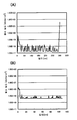
도 10은 실시예 1의 단면 관찰의 결과를 나타낸 도면.
도 11은 실시예 2의 광바이어스 시험의 결과를 나타낸 도면.
도 12는 실시예 3에 관한 도면.
도 13은 실시예 4의 SIMS 분석 깊이 프로파일.BRIEF DESCRIPTION OF THE DRAWINGS The figure which shows the structural example of the transistor of one aspect of this invention.
2 is a diagram showing a method for manufacturing a transistor of one embodiment of the present invention.
3 is a diagram showing a configuration example of a transistor of one embodiment of the present invention.
4 is a diagram showing a configuration example of a transistor of one embodiment of the present invention.
5 illustrates one embodiment of a semiconductor device.
6 illustrates one embodiment of a semiconductor device.
7 illustrates one embodiment of a semiconductor device.
8 illustrates one embodiment of a semiconductor device.
9 illustrates an electronic device.
10 is a view showing the results of cross-sectional observation in Example 1. FIG.
11 shows the results of the optical bias test of Example 2. FIG.
12 is a diagram relating to a third embodiment.
FIG. 13 is a SIMS analysis depth profile of Example 4. FIG.
실시형태에 대하여, 도면을 이용하여 상세하게 설명한다. 단, 본 발명은 이하의 설명에 한정되는 것은 아니고, 본 발명의 취지 및 그 범위로부터 벗어나지 않고, 그 형태 및 상세한 사항을 다양하게 변경할 수 있다는 것은 당업자라면 용이하게 이해할 수 있을 것이다. 따라서, 본 발명은 이하에 나타낸 실시형태의 기재 내용에 한정하여 해석되는 것은 아니다. 또한, 이하에 설명하는 발명의 구성에 있어서, 동일 부분 또는 동일한 기능을 가지는 부분에는 동일한 부호를 다른 도면간에 공통으로 이용하고 그 반복 설명은 생략한다.
EMBODIMENT OF THE INVENTION Embodiment is described in detail using drawing. However, the present invention is not limited to the following description, and it will be easily understood by those skilled in the art that various changes in form and details can be made without departing from the spirit and scope of the present invention. Therefore, this invention is not interpreted limited to description content of embodiment shown below. In addition, in the structure of the invention demonstrated below, the same code | symbol is used for the same part or the part which has the same function in common between different drawings, and the repeated description is abbreviate | omitted.
(실시형태 1)(Embodiment 1)
본 실시형태에서는, 본 발명의 일 양태의 반도체 장치의 구성 및 제작 방법에 대하여 도 1∼도 4를 이용하여 설명한다.In this embodiment, the structure and manufacturing method of the semiconductor device of one embodiment of the present invention will be described with reference to FIGS. 1 to 4.
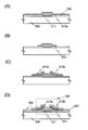
도 1에 반도체 장치의 예로서 트랜지스터(550)를 나타낸다. 도 1(A)에 트랜지스터(550)의 상면도를, 도 1(B)에 트랜지스터(550)의 단면도를 나타낸다. 또한, 도 1(B)은 도 1(A)에 나타낸 절단선 P1-P2의 단면에 상당한다.1 illustrates a
트랜지스터(550)는 절연 표면을 가지는 기판(500) 위에, 제 1 게이트 전극(511), 및 제 1 게이트 전극(511)을 덮는 게이트 절연층(502)을 가진다. 또한, 게이트 절연층(502) 위에 제 1 게이트 전극(511)과 중첩하는 산화물 반도체층(513), 및 산화물 반도체층(513)에 접하고, 단부가 제 1 게이트 전극(511)과 중첩하는 소스 전극 또는 드레인 전극으로서 기능하는 제 1 전극(515a) 및 제 2 전극(515b)을 가진다. 또한, 산화물 반도체층(513)과 중첩하고, 그 일부와 접하는 산화물 절연층(507)을 가진다.The
산화물 반도체층(513)은 수소나 물 등의 불순물이 충분히 제거됨으로써, 또는, 충분한 산소가 공급됨으로써, 고순도화된 것인 것이 바람직하다. 구체적으로는, 예를 들면, 산화물 반도체층(513)의 수소 농도는 5×10¹⁹ atoms/cm3 이하, 바람직하게는 5×10¹⁸ atoms/cm3 이하, 보다 바람직하게는 5×10¹⁷ atoms/cm3 이하로 한다. 또한, 상술한 산화물 반도체층(513) 중 수소 농도는, 2차 이온 질량 분석법(SIMS: Secondary Ion Mass Spectroscopy)으로 측정되는 것이다. 이와 같이, 수소 농도가 충분히 저감되고 고순도화되어, 충분한 산소의 공급에 의해 산소 결핍에 기인하는 에너지 갭 중의 결함 준위가 저감된 산화물 반도체층(513)에서는 캐리어 농도가 1×10¹²/cm3 미만, 바람직하게는, 1×10¹¹/cm3 미만, 보다 바람직하게는 1.45×10¹⁰/cm3 미만이 된다. 예를 들면, 실온(25℃)에서의 오프 전류(여기에서는, 단위 채널폭(1 μm)당의 값)은 100 zA(1 zA(젭토 암페어)는 1×10-21 A) 이하, 바람직하게는 10 zA 이하가 된다. 이와 같이, i형화된 산화물 반도체를 이용함으로써, 양호한 전기 특성의 트랜지스터를 얻을 수 있다.It is preferable that the
또한, 산화물 반도체층(513)의 질소 농도는, 2×10¹⁹ atoms/cm3 이하로 한다. 특히, 질소 농도가 5×10¹⁸ atoms/cm3 이하인 것이 바람직하다. 질소는 산화물 반도체를 구성하는 금속과 결합하기 쉽고, 산화물 반도체층 중에 있어서, 산소와 이 금속의 결합을 방해한다. 산화물 반도체층 중의 질소 농도를 낮게 함으로써, 산화물 반도체층 중의 산소 농도를 충분한 것으로 하고, 산화물 반도체의 전기 특성과 신뢰성을 향상시킬 수 있다.The nitrogen concentration of the
여기에서는, 산화물 반도체층(513)에, In-Ga-Zn-O계 산화물 반도체(인듐(In), 갈륨(Ga), 아연(Zn)을 가지는 산화물 반도체)를 이용한 경우를 예로 들어 설명한다. 산화물 반도체층(513) 중에 질소가 많이 포함되면, 질소와, In이나 Ga가 결합하여, 질화인듐이나 질화갈륨이 생성된다. 산화물 반도체층(513) 중에서, 질소가 In 또는 Ga와 결합하여, 산소와, In 또는 Ga와의 결합을 방해할 수 있다. 산화물 반도체층(513) 중의 질소 농도가 높아지므로, 산화물 반도체층(513)의 캐리어 이동도가 저하된다. 따라서, 산화물 반도체층(513) 중의 질소 농도는 충분히 낮은 것이 바람직하다.Here, the case where In-Ga-Zn-O type oxide semiconductor (oxide semiconductor which has indium (In), gallium (Ga), and zinc (Zn)) is used for the
게이트 절연층(502) 및 산화물 절연층(507)은 산소를 포함하는 절연막을 이용하는 것이 바람직하다. 게이트 절연층(502)이나 산화물 절연층(507)은, 화학양론적 조성비보다 산소가 많은 영역(산소 과잉 영역이라고도 표기함)이 포함되는 막인 것이 보다 바람직하다. 산화물 반도체층(513)과 접하는 게이트 절연층(502) 및 산화물 절연층(507)이 산소 과잉 영역을 가지는 것에 의해, 산화물 반도체층(513)으로부터 게이트 절연층(502) 또는 산화물 절연층(507)으로의 산소의 이동을 막을 수 있다. 또한, 게이트 절연층(502) 또는 산화물 절연층(507)으로부터 산화물 반도체층(513)으로의 산소의 공급을 행할 수도 있다. 따라서, 게이트 절연층(502) 및 산화물 절연층(507)에 협지된 산화물 반도체층(513)을, 충분한 양의 산소를 함유하는 막으로 할 수 있다.As the
특히, 게이트 절연층(502) 및 산화물 절연층(507)은 제 13 족 원소 및 산소를 포함하는 재료를 이용하여 형성하는 것이 바람직하다. 제 13 족 원소 및 산소를 포함하는 재료로서는, 예를 들면, 산화갈륨, 산화알루미늄, 산화알루미늄 갈륨, 산화갈륨 알루미늄의 어느 하나 또는 복수를 포함하는 재료 등이 있다. 여기서, 산화알루미늄 갈륨이란, 갈륨(Ga)의 함유량(원자%)보다 알루미늄(Al)의 함유량(원자%)이 많은 것을 나타내고, 산화갈륨 알루미늄이란, Ga의 함유량(원자%)이 Al의 함유량(원자%) 이상인 것을 나타낸다. 게이트 절연층(502) 및 산화물 절연층(507)은 각각, 상술한 재료를 이용하여 단층 구조, 또는 적층 구조로 형성해도 좋다. 또한, 산화알루미늄은 물을 투과시키기 어렵다는 특성을 가지고 있기 때문에, 산화알루미늄, 산화알루미늄 갈륨, 산화갈륨 알루미늄 등을 적용하는 것은 산화물 반도체막으로의 물의 침입 방지라는 점에서도 바람직하다.In particular, the
상술한 바와 같이, 게이트 절연층(502) 및 산화물 절연층(507)은 화학양론적 조성비보다 산소가 많은 영역을 포함하는 것이 바람직하다. 이것에 의해, 산화물 반도체층(513)과 접하는 절연막 또는 산화물 반도체층(513)에 산소를 공급하고, 산화물 반도체층(513) 중, 또는 산화물 반도체층(513)과 그것에 접하는 절연막과의 계면에서의 산소 결함을 저감할 수 있다. 예를 들면, 게이트 절연층(502)으로서 산화갈륨막을 이용한 경우, Ga2Ox(x = 3+α, 0<α<1)로 하는 것이 바람직하다. 여기서, x는, 예를 들면, 3.3 이상 3.4 이하로 하면 좋다. 또는, 게이트 절연층(502)으로서 산화알루미늄막을 이용한 경우, Al2Ox(x = 3+α, 0<α<1)로 하는 것이 바람직하다. 또는, 게이트 절연층(502)으로서 산화알루미늄 갈륨막을 이용한 경우, GaxAl2-xO3+α(0<x<1, 0<α<1)로 하는 것이 바람직하다. 또는, 게이트 절연층(502)으로서 산화갈륨 알루미늄막을 이용한 경우, GaxAl2-xO3+α(1<x≤2, 0<α<1)로 하는 것이 바람직하다.As described above, the
또한, 산소 결손이 없는 산화물 반도체막을 이용하는 경우, 게이트 절연층 및 산화물 절연층에는, 화학양론적 조성과 일치하는 양의 산소가 포함되어 있으면 좋지만, 트랜지스터의 스레시홀드 전압의 변동을 억제하는 등의 신뢰성을 확보하기 위해서는 산화물 반도체막에 산소 결손 상태가 생길 수 있는 것을 고려하여, 게이트 절연층 및 산화물 절연층에는 화학양론적 조성비보다 많이 산소를 함유시켜 두는 것이 바람직하다.In the case where an oxide semiconductor film having no oxygen deficiency is used, the gate insulating layer and the oxide insulating layer may contain oxygen in an amount consistent with the stoichiometric composition, but the variation of the threshold voltage of the transistor is suppressed. In order to secure the reliability, it is preferable that oxygen be contained in the gate insulating layer and the oxide insulating layer in a larger amount than the stoichiometric composition ratio in consideration of the possibility that an oxygen vacancies may occur in the oxide semiconductor film.
제 1 전극(515a) 및 제 2 전극(515b)은 내열성을 가지고 산소와 반응하기 어려운 금속으로 이루어지고, 예를 들면, 몰리브덴(Mo), 텅스텐(W), 백금(Pt)의 어느 하나 또는 복수를 포함한다. 또는, 금(Au)이나 크롬(Cr)을 이용해도 좋다. 상기 금속은 산화되기 어렵기 때문에, 제 1 전극(515a) 및 제 2 전극(515b)이 산화물 반도체층(513)으로부터 산소를 빼앗는 것을 억제할 수 있다. 또한, 제 1 전극(515a) 및 제 2 전극(515b)의 질소 농도는 2×10¹⁹ atoms/cm3 이하인 것이 바람직하다.The
도 3(A) 및 도 3(B)에 트랜지스터(550)와는 다른 구성의 트랜지스터(551a, 551b)의 단면도를 나타낸다.3A and 3B show cross-sectional views of the
트랜지스터(551a, 551b)는, 각각 절연 표면을 가지는 기판(500) 위에, 제 1 게이트 전극(511), 및 제 1 게이트 전극(511)을 덮는 게이트 절연층(502)을 가진다. 또한, 게이트 절연층(502) 위에 제 1 게이트 전극(511)과 중첩하는 산화물 반도체층(513), 및 산화물 반도체층(513)에 접하는 버퍼층(516a, 516b 또는 516c, 516d), 단부가 제 1 게이트 전극(511)과 중첩하는 소스 전극 또는 드레인 전극으로서 기능하는 제 1 전극(515a) 및 제 2 전극(515b)을 가진다. 또한, 산화물 반도체층(513)과 중첩되고, 그 일부와 접하는 산화물 절연층(507)을 가진다.The
버퍼층은, 산화물 반도체층(513)과, 제 1 전극(515a) 또는 제 2 전극(515b) 사이의 접속 저항을 낮추는 효과를 가진다. 버퍼층의 질소 농도는 2×10¹⁹ atoms/cm3 이하로 한다. 특히, 질소 농도가 5×10¹⁸ atoms/cm3 이하인 것이 바람직하다. 질소는 산화물 반도체를 구성하는 금속과 결합하기 쉽다. 버퍼층은 산화물 반도체층에 접하기 때문에, 버퍼층으로부터 산화물 반도체층에 질소가 침입할 우려가 있다. 산화물 반도체층 중에 침입한 질소는 산소와 이 금속의 결합을 방해한다.The buffer layer has the effect of lowering the connection resistance between the
도 4에 상기에 예시한 트랜지스터와는 다른 구성의 트랜지스터(552)의 단면도를 나타낸다.4 is a sectional view of a
트랜지스터(552)는 절연 표면을 가지는 기판(500) 위에, 제 1 게이트 전극(511), 및 제 1 게이트 전극(511)을 덮는 게이트 절연층(502)을 가진다. 또한, 게이트 절연층(502) 위에 제 1 게이트 전극(511)과 중첩하는 산화물 반도체층(513), 및 산화물 반도체층(513)에 접하고, 단부를 제 1 게이트 전극(511)과 중첩하는 소스 전극 또는 드레인 전극으로서 기능하는 제 1 전극(515a) 및 제 2 전극(515b)을 가진다. 또한, 산화물 반도체층(513)과 중첩되고, 그 일부와 접하는 산화물 절연층(507)을 가진다. 또한, 산화물 절연층(507) 위에, 제 1 게이트 전극(511) 및 산화물 반도체층(513)과 중첩하는 제 2 게이트 전극(519)을 가진다.The
제 2 게이트 전극(519)을 산화물 반도체층(513)의 채널 형성 영역과 중첩되는 위치에 형성하는 것에 의해, 트랜지스터의 신뢰성을 조사하기 위한 바이어스-열 스트레스 시험(이하, BT 시험이라고 함)에 있어서, BT 시험 전후의 트랜지스터 스레시홀드 전압의 변화량을 보다 저감할 수 있다. 또한, 제 2 게이트 전극(519)은 전위가 제 1 게이트 전극(511)과 같아도 좋고, 상이하여도 좋다. 또한, 제 2 게이트 전극(519)의 전위는 GND, 0 V, 혹은 플로팅 상태여도 좋다.By forming the
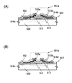
다음에, 트랜지스터(550)를 기판(500) 위에 제작하는 방법에 대하여, 도 2를 이용하여 설명한다.Next, a method of manufacturing the
먼저, 절연 표면을 가지는 기판(500) 위에 도전막을 형성한 후, 제 1 포토리소그래피 공정에 의해 제 1 게이트 전극(511)을 포함하는 배선층을 형성한다. 또한, 레지스트 마스크를 잉크젯법으로 형성해도 좋다. 레지스트 마스크를 잉크젯법으로 형성하면 포토마스크를 사용하지 않기 때문에, 제조 비용을 저감할 수 있다.First, after forming a conductive film on the
본 실시형태에서는 절연 표면을 가지는 기판(500)으로서 유리 기판을 이용한다.In this embodiment, a glass substrate is used as the
하지막이 되는 절연막을 기판(500)과 제 1 게이트 전극(511)과의 사이에 형성해도 좋다. 하지막은 기판(500)으로부터의 불순물 원소의 확산을 방지하는 기능이 있고, 질화실리콘막, 산화실리콘막, 질화산화실리콘막, 또는 산화질화실리콘막을 단층 또는 적층하여 형성할 수 있다.An insulating film serving as a base film may be formed between the
또한, 제 1 게이트 전극(511)은 몰리브덴, 티탄, 탄탈, 텅스텐, 알루미늄, 구리, 네오디뮴, 스칸듐 등의 금속 재료 또는 이것들을 주성분으로 하는 합금 재료를 이용하여, 단층 또는 적층하여 형성할 수 있다.The
다음에, 제 1 게이트 전극(511) 위에 게이트 절연층(502)을 형성한다. 게이트 절연층(502)은 제 13 족 원소 및 산소를 포함하는 재료를 이용하여 형성하는 것이 바람직하다. 예를 들면, 산화갈륨, 산화알루미늄, 산화알루미늄 갈륨, 산화갈륨 알루미늄의 어느 하나 또는 복수를 포함하는 재료 등을 이용할 수 있다. 또한, 게이트 절연층(502)에는 복수 종류의 제 13 족 원소와 산소를 포함시킬 수도 있다. 또는, 제 13 족 원소 외에, 이트륨 등의 제 3 족 원소, 하프늄 등의 제 4 족 원소, 실리콘 등의 제 14 족 원소 등의 수소 이외의 불순물 원소를 포함시킬 수 있다. 이러한 불순물 원소를, 예를 들면 0 초과 20 원자 % 이하 정도 포함시킴으로써, 게이트 절연층(502)의 에너지 갭을 이 원소의 첨가량에 따라 제어할 수 있다.Next, a
게이트 절연층(502)은 그 외에, 산화실리콘이나 산화하프늄을 이용하여 형성해도 좋다.In addition, the
게이트 절연층(502)은 질소, 수소, 물 등의 불순물을 혼입시키지 않는 방법을 이용하여 성막하는 것이 바람직하다. 게이트 절연층(502)에 질소, 수소, 물 등의 불순물이 포함되면, 후에 형성되는 산화물 반도체막에 질소, 수소, 물 등의 불순물의 침입이나, 수소, 물 등의 불순물에 의한 산화물 반도체막 중의 산소의 추출 등에 의해 산화물 반도체막이 저저항화(n형화)하게 되어, 기생 채널이 형성될 우려가 있기 때문이다. 따라서, 게이트 절연층(502)은 가능한 한 질소, 수소, 물 등의 불순물이 포함되지 않게 제작하는 것이 바람직하다. 예를 들면, 스퍼터링법에 의해 성막하는 것이 바람직하다. 성막할 때에 이용하는 스퍼터링 가스로서는, 질소, 수소, 물 등의 불순물이 제거된 고순도 가스를 이용하는 것이 바람직하다.The
스퍼터링법으로서는, 직류 전원을 이용하는 DC 스퍼터링법, 펄스적으로 직류 바이어스를 더하는 펄스 DC 스퍼터링법, 또는 AC 스퍼터링법 등을 이용할 수 있다.As a sputtering method, the DC sputtering method using a DC power supply, the pulse DC sputtering method which adds a direct current bias pulsely, AC sputtering method, etc. can be used.
또한, 게이트 절연층(502)으로서 산화알루미늄 갈륨막 또는 산화갈륨 알루미늄막을 형성할 때에는, 스퍼터링법에 이용하는 타겟으로서 알루미늄 파티클이 첨가된 산화갈륨 타겟을 적용해도 좋다. 알루미늄 파티클이 첨가된 산화갈륨 타겟을 이용함으로써, 타겟의 도전성을 높일 수 있기 때문에, 스퍼터링 시의 방전을 용이한 것으로 할 수 있다. 이러한 타겟을 이용함으로써, 양산화에 적합한 금속 산화물막을 제작할 수 있다.In addition, when forming an aluminum gallium oxide film or a gallium aluminum oxide film as the
다음에, 게이트 절연층(502)에 대하여, 산소 도핑 처리를 행하는 것이 바람직하다. 산소 도핑이란, 산소를 벌크로 첨가하는 것을 말한다. 또한, 이 벌크라는 용어는 산소를 박막 표면뿐만 아니라 박막 내부에 첨가하는 것을 명확하게 하는 취지로 이용하고 있다. 또한, 산소 도핑에는 플라즈마화한 산소를 벌크로 첨가하는 산소 플라즈마 도핑이 포함된다.Next, the oxygen doping treatment is preferably performed on the
게이트 절연층(502)에 대하여, 산소 도핑 처리를 행하는 것에 의해 게이트 절연층(502)에는 화학양론적 조성비보다 산소가 많은 영역이 형성된다. 이러한 영역을 구비함으로써, 후에 성막되는 산화물 반도체막에 산소를 공급하여, 산화물 반도체막 중의 산소 결함을 저감할 수 있다.By performing an oxygen doping process with respect to the
게이트 절연층(502)으로서 산화갈륨막을 이용하는 경우, 산소 도핑을 행함으로써, Ga2Ox(x = 3+α, 0<α<1)로 할 수 있다. x는, 예를 들면, 3.3 이상 3.4 이하로 할 수 있다. 또는, 게이트 절연층(502)으로서 산화알루미늄막을 이용한 경우, 산소 도핑을 행함으로써, Al2Ox(x = 3+α, 0<α<1)로 할 수 있다. 또는, 게이트 절연층(502)으로서 산화알루미늄 갈륨막을 이용하는 경우, 산소 도핑을 행함으로써, GaxAl2 - xO3 +α(0<x<1, 0<α<1)로 할 수 있다. 또는, 게이트 절연층(502)으로서 산화갈륨 알루미늄막을 이용한 경우, 산소 도핑을 행함으로써, GaxAl2-xO3+α(1<x≤2, 0<α<1)로 할 수 있다.When a gallium oxide film is used as the
다음에, 게이트 절연층(502) 위에, 막두께 3 nm 이상 30 nm 이하의 산화물 반도체막(513a)을 스퍼터링법으로 형성한다(도 2(A)). 산화물 반도체막(513a)의 막두께를 너무 크게 하면(예를 들면, 막두께를 50 nm 이상으로 하면), 트랜지스터가 노멀리 온(normally on)이 될 우려가 있기 때문에, 상술한 막두께로 하는 것이 바람직하다. 또한, 게이트 절연층(502), 및 산화물 반도체막(513a)은 대기에 접하지 않게 연속하여 성막하는 것이 바람직하다.Next, an
산화물 반도체막(513a)에 이용하는 산화물 반도체로서는, 4원계 금속 산화물인 In-Sn-Ga-Zn-O계 산화물 반도체나, 3원계 금속 산화물인 In-Ga-Zn-O계 산화물 반도체, In-Sn-Zn-O계 산화물 반도체, In-Al-Zn-O계 산화물 반도체, Sn-Ga-Zn-O계 산화물 반도체, Al-Ga-Zn-O계 산화물 반도체, Sn-Al-Zn-O계 산화물 반도체나, 2원계 금속 산화물인 In-Zn-O계 산화물 반도체, Sn-Zn-O계 산화물 반도체, Al-Zn-O계 산화물 반도체, Zn-Mg-O계 산화물 반도체, Sn-Mg-O계 산화물 반도체, In-Mg-O계 산화물 반도체, In-Ga-O계 산화물 반도체나, 단원계 금속 산화물인 In-O계 산화물 반도체, Sn-O계 산화물 반도체, Zn-O계 산화물 반도체 등을 이용할 수 있다. 또한, 상기 산화물 반도체에 SiO2를 포함해도 좋다. 여기서, 예를 들면, In-Ga-Zn-O계 산화물 반도체란, 인듐(In), 갈륨(Ga), 아연(Zn)을 가지는 산화물 반도체라는 의미이며, 그 화학량론비는 특별히 따지지 않는다. 또한, In, Ga, Zn 이외의 원소를 포함해도 좋다.Examples of the oxide semiconductor used for the
또한, 산화물 반도체막(513a)은 화학식 InMO3(ZnO)m(m>0)으로 표기되는 박막을 이용할 수 있다. 여기서, M은 Ga, Al, Mn 및 Co로부터 선택된 하나 또는 복수의 금속 원소를 나타낸다. 예를 들면, M으로서 Ga, Ga 및 Al, Ga 및 Mn, 또는 Ga 및 Co 등이 있다.As the
또한, 산화물 반도체로서 In-Zn-O계의 재료를 이용하는 경우, 이용하는 타겟의 조성비는 원자수비로, In : Zn = 50 : 1∼1 : 2(몰수비로 환산하면 In2O3 : ZnO = 25 : 1∼1 : 4), 바람직하게는 In : Zn = 20 : 1∼1 : 1(몰수비로 환산하면 In2O3 : ZnO = 10 : 1∼1 : 2), 더욱 바람직하게는 In : Zn = 15 : 1∼1.5 : 1(몰수비로 환산하면 In2O3 : ZnO = 15 : 2∼3 : 4)로 한다. 예를 들면, In-Zn-O계 산화물 반도체의 형성에 이용하는 타겟은 원자수비가 In : Zn : O = X : Y : Z 일 때, Z>1.5X+Y로 한다.In the case of using an In—Zn—O-based material as the oxide semiconductor, the composition ratio of the target to be used is an atomic ratio, and In: Zn = 50: 1 to 1: 2 (in terms of molar ratio), In 2 O 3 : ZnO = 25 1: 1: 4), preferably In: Zn = 20: 1: 1: 1 (in terms of molar ratios, In 2 O 3 : ZnO = 10: 1: 1: 2), more preferably In: Zn = 15: 1-1.5: 1 (In 2 O 3 : ZnO = 15: 2-3: 4). For example, the target used for formation of an In—Zn—O-based oxide semiconductor is Z> 1.5X + Y when the atomic ratio is In: Zn: O = X: Y: Z.
본 실시형태에서는, 산화물 반도체막(513a)으로서 In-Ga-Zn-O계 산화물 타겟을 이용하여 스퍼터링법에 의해 성막한다. 또한, 산화물 반도체막(513a)은 희가스(대표적으로는 아르곤) 분위기하, 산소 분위기하, 또는 희가스와 산소의 혼합 분위기 하에서 스퍼터링법에 의해 형성할 수 있다.In this embodiment, a film is formed by sputtering using an In—Ga—Zn—O-based oxide target as the
산화물 반도체막(513a)으로서 In-Ga-Zn-O막을 스퍼터링법으로 제작하기 위한 타겟으로서는 예를 들면, 조성비로서 In2O3 : Ga2O3 : ZnO = 1 : 1 : 1[mol수비]의 산화물 타겟을 이용할 수 있다. 또한, 이 타겟의 재료 및 조성에 한정되지 않고, 예를 들면, In2O3 : Ga2O3 : ZnO = 1 : 1 : 2[mol수비]의 산화물 타겟을 이용해도 좋다.As a target for producing the In-Ga-Zn-O film as the
또한, 산화물 타겟의 충전율은 90% 이상 100% 이하, 바람직하게는 95% 이상 99.9% 이하이다. 충전율이 높은 금속 산화물 타겟을 이용함으로써, 성막한 산화물 반도체막(513a)은 치밀한 막으로 할 수 있다.The filling rate of the oxide target is 90% or more and 100% or less, preferably 95% or more and 99.9% or less. By using the metal oxide target with a high filling rate, the
산화물 반도체막(513a)을 성막할 때에 이용하는 스퍼터링 가스로서는 질소, 수소, 물, 수산기 또는 수소화물 등의 불순물이 제거된 고순도 가스를 이용하는 것이 바람직하다.As the sputtering gas used for forming the
산화물 반도체막(513a)의 성막은 감압 상태로 보유된 성막실 내에 기판(500)을 보유하고, 기판 온도를 100℃ 이상 600℃ 이하 바람직하게는 200℃ 이상 400℃ 이하로 하여 행한다. 기판(500)을 가열하면서 성막함으로써, 성막한 산화물 반도체막(513a)에 포함되는 불순물 농도를 저감할 수 있다. 또한, 스퍼터링에 의한 손상이 경감된다. 그리고, 성막실 내의 잔류 수분을 제거하면서 수소 및 물이 제거된 스퍼터링 가스를 도입하고, 상기 타겟을 이용하여 기판(500) 위에 산화물 반도체막(513a)을 성막한다. 성막실 내의 잔류 수분을 제거하기 위해서는, 흡착형의 진공 펌프, 예를 들면, 크라이오 펌프, 이온 펌프, 티탄 서브리메이션 펌프를 이용하는 것이 바람직하다. 또한, 배기 수단은 터보 펌프에 콜드 트랩을 더한 것이어도 좋다. 크라이오 펌프를 이용하여 배기한 성막실은 예를 들면, 수소 원자, 물 등 수소 원자를 포함하는 화합물 및 질소(보다 바람직하게는 탄소 원자를 포함하는 화합물) 등이 배기되기 때문에, 이 성막실에서 성막한 산화물 반도체막(513a)에 포함되는 불순물의 농도를 저감할 수 있다.The film formation of the
성막 조건의 일례로서는, 기판과 타겟 사이의 거리를 100 mm, 압력 0.6 Pa, 직류(DC) 전원 0.5 kW, 산소(산소 유량 비율 100%) 분위기하의 조건이 적용된다. 또한, 펄스 직류 전원을 이용하면, 성막 시에 발생하는 분상 물질(파티클, 먼지라고도 함)을 경감할 수 있어, 막두께 분포도 균일하게 되기 때문에 바람직하다.As an example of film-forming conditions, the distance between a board | substrate and a target is 100 mm, the pressure 0.6 Pa, the DC power supply 0.5 kW, and oxygen (100% of oxygen flow rate ratio) conditions are applied. In addition, the use of a pulsed DC power supply is preferable because it can reduce powdery substances (also called particles and dust) generated during film formation and make the film thickness distribution uniform.
그 후, 산화물 반도체막(513a)에 대하여, 열처리(제 1 열처리)를 행하는 것이 바람직하다. 이 제 1 열처리에 의해 산화물 반도체막(513a) 중의 과잉의 수소(물이나 수산기를 포함함)를 제거할 수 있다. 또한, 이 제 1 열처리에 의해, 게이트 절연층(502) 중의 과잉의 수소(물이나 수산기를 포함함)를 제거하는 것도 가능하다. 제 1 열처리의 온도는 250℃ 이상 700℃ 이하, 바람직하게는 450℃ 이상 600℃ 이하, 또는 기판의 변형점 미만으로 한다.Thereafter, heat treatment (first heat treatment) is preferably performed on the
열처리는 예를 들면, 저항 발열체 등을 이용한 전기로에 피처리물을 도입하고, 질소 분위기하, 450℃, 1시간의 조건에서 행할 수 있다. 이 동안, 산화물 반도체막(513a)은 대기에 노출되지 않게 하고, 물이나 수소의 혼입이 생기지 않도록 한다.For example, the heat treatment can be performed by introducing a workpiece into an electric furnace using a resistive heating element or the like, and performing the conditions under a nitrogen atmosphere at 450 ° C. for 1 hour. In the meantime, the
열처리 장치는 전기로에 한정되지 않고, 가열된 가스 등의 매체로부터의 열전도, 또는 열복사에 의해, 피처리물을 가열하는 장치를 이용해도 좋다. 예를 들면, GRTA(Gas Rapid Thermal Anneal) 장치, LRTA(Lamp Rapid Thermal Anneal) 장치 등의 RTA(Rapid Thermal Anneal) 장치를 이용할 수 있다. LRTA 장치는 할로겐 램프, 메탈 할라이드 램프, 크세논 아크 램프, 카본 아크 램프, 고압 나트륨 램프, 고압 수은 램프 등의 램프로부터 발하는 광(전자파)의 복사에 의해, 피처리물을 가열하는 장치이다. GRTA 장치는 고온의 가스를 이용하여 열처리를 행하는 장치이다. 가스로서는, 아르곤 등의 희가스, 또는 질소와 같은, 열처리에 의해 피처리물과 반응하지 않는 불활성 기체가 이용된다.The heat treatment apparatus is not limited to an electric furnace, and an apparatus for heating a workpiece by heat conduction or heat radiation from a medium such as heated gas may be used. For example, a Rapid Thermal Anneal (RTA) device such as a Gas Rapid Thermal Anneal (GRTA) device or a Lamp Rapid Thermal Anneal (LRTA) device may be used. The LRTA apparatus is an apparatus for heating a target object by radiation of light (electromagnetic waves) emitted from lamps such as halogen lamps, metal halide lamps, xenon arc lamps, carbon arc lamps, high pressure sodium lamps, and high pressure mercury lamps. GRTA apparatus is an apparatus which heat-processes using high temperature gas. As the gas, a rare gas such as argon, or an inert gas that does not react with the object to be processed by heat treatment, such as nitrogen, is used.
예를 들면, 제 1 열처리로서, 가열된 불활성 가스 분위기 중에 피처리물을 투입하고, 수 분간 가열한 후, 이 불활성 가스 분위기로부터 피처리물을 취출하는 GRTA 처리를 행하여도 좋다. GRTA 처리를 이용하면 단시간에서의 고온 열처리가 가능하게 된다. 또한, 피처리물의 내열 온도를 넘는 온도 조건이어도 적용이 가능하게 된다. 또한, 처리 중에 불활성 가스를, 산소를 포함하는 가스로 전환해도 좋다. 산소를 포함하는 분위기에서 제 1 열처리를 행함으로써, 산소 결손에 기인하는 에너지 갭 중의 결함 준위를 저감할 수 있기 때문이다.For example, as a 1st heat processing, you may inject a to-be-processed object in the heated inert gas atmosphere, and after heating for several minutes, you may perform GRTA process which takes out a to-be-processed object from this inert gas atmosphere. GRTA treatment enables high temperature heat treatment in a short time. Moreover, application is possible even if it is a temperature condition exceeding the heat-resistant temperature of a to-be-processed object. In addition, you may convert inert gas into the gas containing oxygen during a process. This is because the defect level in the energy gap caused by oxygen deficiency can be reduced by performing the first heat treatment in an atmosphere containing oxygen.
또한, 불활성 가스 분위기로서는, 질소, 또는 희가스(헬륨, 네온, 아르곤 등)를 주성분으로 하는 분위기이며, 물, 수소 등이 포함되지 않는 분위기를 적용하는 것이 바람직하다. 예를 들면, 열처리 장치에 도입하는 질소나, 헬륨, 네온, 아르곤 등의 희가스의 순도를, 6 N(99.9999%) 이상, 바람직하게는 7 N(99.99999%) 이상(즉, 불순물 농도가 1 ppm 이하, 바람직하게는 0.1 ppm 이하)으로 한다.Moreover, as an inert gas atmosphere, it is the atmosphere which has nitrogen or a rare gas (helium, neon, argon etc.) as a main component, and it is preferable to apply the atmosphere which does not contain water, hydrogen, etc. For example, the purity of nitrogen, helium, neon, argon, or the like, which is introduced into the heat treatment apparatus, is 6 N (99.9999%) or more, preferably 7 N (99.99999%) or more (ie, impurity concentration is 1 ppm). Or less, preferably 0.1 ppm or less).
그런데, 상술한 열처리(제 1 열처리)에는 수소나 물 등을 제거하는 효과가 있기 때문에, 이 열처리를 탈수화 처리나, 탈수소화 처리 등이라고 부를 수도 있다. 이 탈수화 처리나 탈수소화 처리는, 예를 들면, 산화물 반도체막(513a)을 섬 형상으로 가공한 후 등의 타이밍에서 행하는 것도 가능하다. 또한, 이러한 탈수화 처리, 탈수소화 처리는 1회에 한정되지 않고 복수회 행하여도 좋다.By the way, since the heat treatment mentioned above (the 1st heat treatment) has the effect of removing hydrogen, water, etc., this heat treatment can also be called dehydration process, dehydrogenation process, etc. This dehydration process and dehydrogenation process can also be performed at the timing, such as after processing the
또한, 산화물 반도체막(513a)에 접하는 게이트 절연층(502)은 산소 도핑 처리되어 있어, 산소 과잉 영역을 가진다. 따라서, 산화물 반도체막(513a)으로부터, 게이트 절연층(502)으로의 산소의 이동을 억제할 수 있다. 또한, 산소 도핑 처리된 게이트 절연층(502)과 접하여 산화물 반도체막(513a)을 적층함으로써, 게이트 절연층(502)으로부터 산화물 반도체막(513a)으로 산소를 공급할 수 있다. 게이트 절연층(502)으로부터의 산화물 반도체막(513a)으로의 산소의 공급은, 산소 도핑 처리된 게이트 절연층(502)과 산화물 반도체막(513a)이 접한 상태에서 열처리를 행하는 것에 의해, 보다 촉진된다.In addition, the
또한, 게이트 절연층(502)에 첨가되고, 산화물 반도체막(513a)에 공급되는 산소의 적어도 일부는, 산소의 미결합수(댕글링 본드)를 산화물 반도체 중에서 가지는 것이 바람직하다. 미결합수(댕글링 본드)를 가짐으로써, 산화물 반도체막 중에 잔존할 수 있는 수소와 결합하여, 수소를 고정화(비가동 이온화)할 수 있기 때문이다.In addition, it is preferable that at least a part of oxygen added to the
다음에, 산화물 반도체막(513a)을 제 2 포토리소그래피 공정에 의해 섬 형상의 산화물 반도체층(513)으로 가공하는 것이 바람직하다(도 2(B)). 또한, 섬 형상의 산화물 반도체층(513)을 형성하기 위한 레지스트 마스크를 잉크젯법으로 형성해도 좋다. 레지스트 마스크를 잉크젯법으로 형성하면 포토마스크를 사용하지 않기 때문에, 제조 비용을 저감할 수 있다. 섬 형상의 산화물 반도체층(513)을 형성하기 위한 에칭은 드라이 에칭이어도 웨트 에칭이어도 좋고, 양쪽 모두를 이용해도 좋다.Next, it is preferable to process the
다음에, 게이트 절연층(502) 및 산화물 반도체층(513) 위에, 소스 전극 및 드레인 전극(이것과 같은 층에서 형성되는 배선을 포함함)을 형성하기 위한 도전막을 형성한다. 소스 전극 및 드레인 전극에 이용하는 도전막으로서는, 내열성을 가지고 산소와 반응하기 어려운 금속을 이용하여 형성하면 좋다. 특히, Mo, W, Pt 중 어느 하나 또는 복수를 포함하는 것이 바람직하다. 그 외에, Au, Cr 등도 이용할 수 있다. 도전막은 질소를 혼입시키지 않는 방법을 이용하여 성막하는 것이 바람직하다.Next, on the
제 3 포토리소그래피 공정에 의해 도전막 위에 레지스트 마스크를 형성하고, 선택적으로 에칭을 행하여 제 1 전극(515a), 제 2 전극(515b)을 형성한 후, 레지스트 마스크를 제거한다(도 2(C)). 제 3 포토리소그래피 공정에서의 레지스트 마스크 형성 시의 노광에는, 자외선이나 KrF 레이저광이나 ArF 레이저광을 이용하면 좋다. 산화물 반도체층(513) 위에서 서로 인접하는 제 1 전극(515a)의 하단부와 제 2 전극(515b)의 하단부의 간격폭에 의해 후에 형성되는 트랜지스터의 채널 길이(L)가 결정된다. 또한, 채널 길이 L = 25 nm 미만의 노광을 행하는 경우에는, 예를 들면, 수 nm∼수 10 nm로 매우 파장이 짧은 초자외선(Extreme Ultraviolet)을 이용하여 제 3 포토리소그래피 공정에서의 레지스트 마스크 형성 시의 노광을 행하면 좋다. 초자외선에 의한 노광은 해상도가 높고 초점심도도 크다. 따라서, 후에 형성되는 트랜지스터의 채널 길이(L)를 미세화하는 것이 가능하고, 회로의 동작 속도를 고속화할 수 있다.A resist mask is formed on the conductive film by the third photolithography step, and selectively etched to form the
또한, 포토리소그래피 공정에서 이용하는 포토마스크수 및 공정수를 삭감하기 위해, 투과한 광이 복수의 강도가 되는 노광 마스크인 다계조 마스크에 의해 형성된 레지스트 마스크를 이용하여 에칭 공정을 행하여도 좋다. 다계조 마스크를 이용하여 형성한 레지스트 마스크는 복수의 막두께를 가지는 형상이 되어, 에칭을 행함으로서 더욱 형상을 변형할 수 있기 때문에, 다른 패턴으로 가공하는 복수의 에칭 공정에 이용할 수 있다. 따라서, 한 장의 다계조 마스크에 의해, 적어도 2종류 이상의 다른 패턴에 대응하는 레지스트 마스크를 형성할 수 있다. 따라서 노광 마스크수를 삭감할 수 있고, 대응하는 포토리소그래피 공정도 삭감할 수 있기 때문에, 공정의 간략화가 가능하게 된다.Further, in order to reduce the number of photomasks and the number of steps used in the photolithography step, the etching step may be performed using a resist mask formed by a multi-gradation mask that is an exposure mask whose transmitted light has a plurality of intensities. Since the resist mask formed using a multi-gradation mask becomes a shape which has a some film thickness, and can shape-deform further by performing an etching, it can be used for the some etching process processed into a different pattern. Therefore, a resist mask corresponding to at least two or more types of different patterns can be formed by one multi-tone mask. Therefore, since the number of exposure masks can be reduced and the corresponding photolithography process can also be reduced, the process can be simplified.
또한, 도전막의 에칭 시에, 산화물 반도체층(513)이 에칭되어, 분단하는 일이 없도록 에칭 조건을 최적화하는 것이 바람직하다. 그러나, 도전막만을 에칭하고, 산화물 반도체층(513)을 전혀 에칭하지 않는다는 조건을 얻기는 어렵고, 도전막의 에칭 시에 산화물 반도체층(513)은 일부만이 에칭되어, 예를 들면, 산화물 반도체층(513)의 막두께의 5 내지 50%가 에칭되어, 홈부(오목부)를 가지는 산화물 반도체층(513)이 될 수도 있다.In addition, it is preferable to optimize the etching conditions so that the
다음에, N2O, N2, 또는 Ar 등의 가스를 이용한 플라즈마 처리를 행하여, 노출된 산화물 반도체층(513)의 표면에 부착한 흡착수 등을 제거해도 좋다. 플라즈마 처리를 행한 경우, 이 플라즈마 처리에 이어 대기에 접하는 일 없이, 산화물 반도체층(513)에 접하는 산화물 절연층(507)을 형성하는 것이 바람직하다.Next, plasma treatment using a gas such as N 2 O, N 2 , or Ar may be performed to remove adsorbed water or the like adhering to the exposed
다음에, 제 1 전극(515a), 및 제 2 전극(515b)을 덮고, 또한 산화물 반도체층(513)의 일부와 접하는 산화물 절연층(507)을 형성한다(도 2(D)). 산화물 절연층(507)은 게이트 절연층(502)과 같은 재료, 같은 공정으로 형성할 수 있다.Next, an
다음에, 산화물 절연층(507)에 대하여, 산소 도핑 처리를 행하는 것이 바람직하다. 산화물 절연층(507)에 대하여, 산소 도핑 처리를 행함으로써, 산화물 절연층(507)에는 화학양론적 조성비보다 산소가 많은 영역이 형성된다. 이러한 영역을 구비함으로써, 산화물 반도체층에 산소를 공급하여, 산화물 반도체층 중의 산소 결함을 저감할 수 있다.Next, the oxygen doping treatment is preferably performed on the
다음에 산화물 반도체층(513)이 산화물 절연층(507)과 일부(채널 형성 영역)가 접한 상태로 제 2 열처리를 행하는 것이 바람직하다. 제 2 열처리의 온도는 250℃ 이상 700℃ 이하, 바람직하게는 450℃ 이상 600℃ 이하, 또는 기판의 변형점 미만으로 한다.Next, the
제 2 열처리는 질소, 산소, 건조 공기(물의 함유량이 20 ppm 이하, 바람직하게는 1 ppm 이하, 보다 바람직하게는 10 ppb 이하의 공기), 또는 희가스(아르곤, 헬륨 등)의 분위기하에서 행하면 좋지만, 상기 질소, 산소, 건조 공기, 또는 희가스 등의 분위기에 물, 수소 등이 포함되지 않는 것이 바람직하다. 또한, 가열 처리 장치에 도입하는 질소, 산소, 또는 희가스의 순도를, 6 N(99.9999%) 이상 바람직하게는 7 N(99.99999%) 이상(즉 불순물 농도를 1 ppm 이하, 바람직하게는 0.1 ppm 이하)으로 하는 것이 바람직하다.The second heat treatment may be performed in an atmosphere of nitrogen, oxygen, dry air (water content of 20 ppm or less, preferably 1 ppm or less, more preferably 10 ppb or less), or a rare gas (argon, helium, etc.), It is preferable that water, hydrogen, etc. are not contained in atmosphere, such as said nitrogen, oxygen, dry air, or rare gas. In addition, the purity of nitrogen, oxygen, or rare gas introduced into the heat treatment apparatus is 6 N (99.9999%) or more, preferably 7 N (99.99999%) or more (that is, impurity concentration is 1 ppm or less, preferably 0.1 ppm or less). It is preferable to make it).
제 2 열처리에 있어서는, 산화물 반도체층(513)과 게이트 절연층(502) 및 산화물 절연층(507)이 접한 상태로 가열된다. 따라서, 상술한 탈수화(또는 탈수소화) 처리에 의해 동시에 감소하게 될 가능성이 있는 산화물 반도체를 구성하는 주성분 재료의 하나인 산소를, 산소를 포함하는 게이트 절연층(502) 및 산화물 절연층(507)으로부터 산화물 반도체층(513)으로 공급할 수 있다. 이상의 공정으로 고순도화되고, 전기적으로 i형(진성)화된 산화물 반도체층(513)을 형성할 수 있다.In the second heat treatment, the
위에서 설명한 바와 같이, 제 1 열처리와 제 2 열처리를 적용함으로써, 산화물 반도체층(513)을 그 주성분 이외의 불순물이 극력 포함되지 않도록 고순도화할 수 있다. 고순도화된 산화물 반도체층(513) 중에는 도너에 유래하는 캐리어가 매우 적고(제로에 가까움), 캐리어 농도는 1×10¹⁴/cm3 미만, 바람직하게는 1×10¹²/cm3 미만, 더욱 바람직하게는 1×10¹¹/cm3 미만이다.As described above, by applying the first heat treatment and the second heat treatment, the
이상의 공정으로 트랜지스터(550)가 형성된다. 트랜지스터(550)는 수소, 물, 수산기 또는 수소화물(수소 화합물이라고도 함) 등의 불순물을 산화물 반도체층(513)으로부터 의도적으로 배제하여, 고순도화된 산화물 반도체층(513)을 포함하는 트랜지스터이다. 또한, 산화물 반도체층(513)은 질소 농도가 충분히 저감되어 있다(질소 농도가 2×10¹⁹ atoms/cm3 이하임). 또한, 제 1 전극(515a) 및 제 2 전극(515b)은 산소와 반응하기 어려운 금속으로 이루어진다. 따라서, 트랜지스터(550)는 전기적 특성 변동이 억제되어 있어, 전기적으로 안정적이다.The
또한, 도시하지 않았지만, 트랜지스터(550)를 덮도록, 보호 절연막을 더 형성해도 좋다. 보호 절연막으로서는 질화규소막, 질화산화규소막, 또는 질화알루미늄막 등을 이용할 수 있다.Although not shown, a protective insulating film may be further formed to cover the
또한, 트랜지스터(550) 위에 평탄화 절연막을 형성해도 좋다. 평탄화 절연막의 재료로서는, 아크릴, 폴리이미드, 벤조시클로부텐, 폴리아미드, 에폭시 등의 내열성을 가지는 유기 재료를 이용할 수 있다. 또한 상기 유기 재료 외에, 저유전율 재료(low-k 재료), 실록산계 수지, PSG(인 유리), BPSG(인 붕소 유리) 등을 이용할 수 있다. 또한, 이들 재료로 형성되는 절연막을 복수 적층시켜도 좋다.In addition, a planarization insulating film may be formed on the
또한, 후의 소스 전극, 및 드레인 전극이 되는 도전막을 성막하기 전에, 산화물 반도체층(513) 위에 버퍼층(516a, 516b)(또는, 버퍼층(516c, 516d))을 형성함으로써, 도 3(A) 및 도 3(B)에 나타낸 트랜지스터(551a)나 트랜지스터(551b)를 형성할 수 있다. 버퍼층으로서는, 예를 들면, ITO막 등의 투명 도전막을 이용할 수 있다. 산화물 반도체층(513) 위에 도전막을 형성하고, 포토리소그래피 공정에 의해 이 도전막 위에 레지스트 마스크를 형성하고, 선택적으로 에칭을 행하여 버퍼층(516a, 516b)을 형성한 후, 레지스트 마스크를 제거하면 좋다.3A and 3B,
또한, 산화물 절연층(507) 위이고, 산화물 반도체층(513)의 채널 형성 영역과 중첩하는 영역에 제 2 게이트 전극(519)을 형성함으로써, 도 4에 나타낸 트랜지스터(552)를 형성할 수 있다. 제 2 게이트 전극(519)은 제 1 게이트 전극(511)과 같은 재료, 같은 공정으로 형성할 수 있다. 제 2 게이트 전극(519)을 산화물 반도체층(513)의 채널 형성 영역과 중첩하는 위치에 형성하는 것에 의해, BT 시험 전후에 있어서의 트랜지스터의 스레시홀드 전압의 변화량을 보다 저감할 수 있다. 또한, 제 2 게이트 전극(519)은 전위가 제 1 게이트 전극(511)과 같아도 좋고, 상이하여도 좋다. 또한, 제 2 게이트 전극(519)의 전위는 GND, 0 V, 혹은 플로팅 상태여도 좋다.In addition, by forming the
이상과 같이, 본 발명의 일 양태의 트랜지스터는, 산화물 반도체층 중의 질소 농도가 저감되고, 또한, 소스 전극 및 드레인 전극에 내열성을 가지고 산화되기 어려운 금속을 이용하기 때문에, 산화물 반도체층 중의 산소와 금속의 결합이 방해되는 것을 억제할 수 있다. 따라서, 산화물 반도체를 이용한 트랜지스터의 전기 특성과 신뢰성을 향상시킬 수 있다. 예를 들면, 광열화에 의한 트랜지스터 특성의 변동을 저감할 수 있다.
As described above, in the transistor of one embodiment of the present invention, since the nitrogen concentration in the oxide semiconductor layer is reduced, and the metal which is difficult to oxidize with heat resistance is used for the source electrode and the drain electrode, oxygen and the metal in the oxide semiconductor layer are used. It can suppress that the binding of is interrupted. Therefore, the electrical characteristics and the reliability of the transistor using the oxide semiconductor can be improved. For example, variations in transistor characteristics due to photodeterioration can be reduced.
(실시형태 2)(Embodiment 2)
실시형태 1에 예시한 트랜지스터를 이용하여 표시 기능을 가지는 반도체 장치(표시 장치라고도 함)를 제작할 수 있다. 또한, 트랜지스터를 포함하는 구동 회로의 일부 또는 전체를, 화소부와 같은 기판 위에 일체 형성하여, 시스템 온 패널(system-on-panel)을 형성할 수 있다.A semiconductor device (also called a display device) having a display function can be manufactured using the transistors exemplified in the first embodiment. In addition, a part or all of the driving circuit including the transistor may be integrally formed on a substrate such as a pixel portion to form a system-on-panel.
도 5(A)에서, 제 1 기판(4001) 위에 형성된 화소부(4002)를 둘러싸도록 하여, 시일재(4005)가 형성되고, 제 2 기판(4006)에 의해 봉지되어 있다. 도 5(A)에서는, 제 1 기판(4001) 위의 시일재(4005)에 의해 둘러싸여 있는 영역과는 다른 영역에, 별도 준비된 기판 위에 단결정 반도체막 또는 다결정 반도체막으로 형성된 주사선 구동 회로(4004), 신호선 구동 회로(4003)가 실장되어 있다. 또한 별도 형성된 신호선 구동 회로(4003)와 주사선 구동 회로(4004) 또는 화소부(4002)에 부여되는 각종 신호 및 전위는, FPC(Flexible Printed Circuit)(4018a, 4018b)로부터 공급된다.In Fig. 5A, the sealing
도 5(B) 및 도 5(C)에서, 제 1 기판(4001) 위에 형성된 화소부(4002)와 주사선 구동 회로(4004)를 둘러싸도록 하여, 시일재(4005)가 제공된다. 또한 화소부(4002)와 주사선 구동 회로(4004) 위에 제 2 기판(4006)이 설치되어 있다. 따라서 화소부(4002)와 주사선 구동 회로(4004)는, 제 1 기판(4001)과 시일재(4005)와 제 2 기판(4006)에 의해, 표시 소자와 함께 봉지되어 있다. 도 5(B) 및 도 5(C)에서는, 제 1 기판(4001) 위의 시일재(4005)에 의해 둘러싸여 있는 영역과는 다른 영역에, 별도 준비된 기판 위에 단결정 반도체막 또는 다결정 반도체막으로 형성된 신호선 구동 회로(4003)가 실장되어 있다. 도 5(B) 및 도 5(C)에서는, 별도 형성된 신호선 구동 회로(4003)와 주사선 구동 회로(4004) 또는 화소부(4002)에 부여되는 각종 신호 및 전위는 FPC(4018)로부터 공급된다.5B and 5C, a sealing
또한, 도 5(B) 및 도 5(C)에서는, 신호선 구동 회로(4003)를 별도 형성하여, 제 1 기판(4001)에 실장하고 있는 예를 나타내고 있지만, 이 구성에 한정되는 것은 아니다. 주사선 구동 회로를 별도 형성하여 실장해도 좋고, 신호선 구동 회로의 일부 또는 주사선 구동 회로의 일부만을 별도 형성하여 실장해도 좋다.5B and 5C show an example in which the signal
또한, 별도 형성한 구동 회로의 접속 방법은 특별히 한정되는 것은 아니고, COG(Chip On Glass) 방법, 와이어 본딩 방법, 혹은 TAB(Tape Automated Bonding) 방법 등을 이용할 수 있다. 도 5(A)는 COG 방법에 의해 신호선 구동 회로(4003), 주사선 구동 회로(4004)를 실장하는 예이며, 도 5(B)는 COG 방법에 의해 신호선 구동 회로(4003)를 실장하는 예이며, 도 5(C)는 TAB 방법에 의해 신호선 구동 회로(4003)를 실장하는 예이다.In addition, the connection method of the drive circuit formed separately is not specifically limited, A COG (Chip On Glass) method, a wire bonding method, the Tape Automated Bonding (TAB) method, etc. can be used. 5A is an example in which the signal
또한, 표시 장치는 표시 소자가 봉지된 상태에 있는 패널과, 이 패널에 컨트롤러를 포함하는 IC 등을 실장한 상태에 있는 모듈을 포함한다.The display device also includes a panel in which the display element is sealed, and a module in a state in which an IC including a controller is mounted on the panel.
또한, 본 명세서 중에서의 표시 장치란, 화상 표시 디바이스, 표시 디바이스, 혹은 광원(조명 장치 포함함)을 가리킨다. 또한, 커넥터, 예를 들면 FPC 혹은 TAB 테이프 혹은 TCP가 장착된 모듈, TAB 테이프나 TCP의 끝에 프린트 배선판이 설치된 모듈, 또는 표시 소자에 COG 방식에 의해 IC(집적회로)가 직접 실장된 모듈도 모두 표시 장치에 포함하는 것으로 한다.In addition, the display apparatus in this specification refers to an image display device, a display device, or a light source (including an illumination device). In addition, a connector, for example, a module equipped with an FPC or TAB tape or TCP, a module with a printed wiring board at the end of the TAB tape or TCP, or a module in which an IC (integrated circuit) is directly mounted by a COG method on a display element can be used. It is assumed that it is included in the display device.
또한 제 1 기판 위에 형성된 화소부 및 주사선 구동 회로는, 트랜지스터를 복수 가지고 있고, 실시형태 1에 일례를 나타낸 본 발명의 일 양태의 트랜지스터를 적용할 수 있다.The pixel portion and the scanning line driver circuit formed on the first substrate have a plurality of transistors, and the transistor of one embodiment of the present invention shown in Example 1 can be applied.
표시 장치에 형성되는 표시 소자로서는 액정 소자(액정 표시 소자라고도 함), 발광 소자(발광 표시 소자라고도 함)를 이용할 수 있다. 발광 소자는 전류 또는 전압에 의해 휘도가 제어되는 소자를 그 범주에 포함하고 있고, 구체적으로는 무기 EL(Electro Luminescence), 유기 EL 등이 포함된다. 또한, 전자 잉크 등 전기적 작용에 의해 콘트라스트가 변화하는 표시 매체도 적용할 수 있다.As a display element formed in a display apparatus, a liquid crystal element (also called liquid crystal display element) and a light emitting element (also called light emitting display element) can be used. The light emitting device includes, in its category, an element whose luminance is controlled by current or voltage, and specifically includes an inorganic EL (Electro Luminescence), an organic EL, and the like. Also, a display medium whose contrast is changed by an electrical action such as an electronic ink can be applied.
반도체 장치의 일 형태에 대하여, 도 6 내지 도 8을 이용하여 설명한다. 도 6(B), 도 7 및 도 8은 도 5(B)의 M-N의 단면도에 상당한다. 도 6(A)은 도 6(B)에 나타낸 트랜지스터(4010)의 상면도에 상당한다.One embodiment of the semiconductor device will be described with reference to FIGS. 6 to 8. FIG. 6 (B), FIG. 7 and FIG. 8 correspond to sectional drawing of M-N of FIG. 5 (B). FIG. 6A corresponds to a top view of the
도 6 내지 도 8에 나타낸 바와 같이, 반도체 장치는 접속 단자 전극(4015) 및 단자 전극(4016)을 가지고 있고, 접속 단자 전극(4015) 및 단자 전극(4016)은 FPC(4018)가 가지는 단자와 이방성 도전막(4019)을 통하여 전기적으로 접속되어 있다.As shown in FIGS. 6 to 8, the semiconductor device has a connecting
접속 단자 전극(4015)은 제 1 전극(4030)과 같은 도전막으로 형성되고, 단자 전극(4016)은 트랜지스터(4010), 트랜지스터(4011)의 소스 전극 및 드레인 전극과 같은 도전막으로 형성되어 있다.The
또한, 제 1 기판(4001) 위에 형성된 화소부(4002)와 주사선 구동 회로(4004)는 트랜지스터를 복수 가지고 있고, 도 6 내지 도 8에서는, 화소부(4002)에 포함되는 트랜지스터(4010)와 주사선 구동 회로(4004)에 포함되는 트랜지스터(4011)를 예시하고 있다.The
트랜지스터(4010), 트랜지스터(4011)로서 본 발명의 일 양태의 트랜지스터를 적용할 수 있다. 본 발명의 일 양태의 트랜지스터는, 전기적 특성 변동이 억제되어, 전기적으로 안정적이다. 따라서, 도 6 내지 도 8에 나타낸 본 실시형태의 반도체 장치로서 신뢰성이 높은 반도체 장치를 제공할 수 있다.The transistor of one embodiment of the present invention can be used as the
화소부(4002)에 설치된 트랜지스터(4010)는 표시 소자와 전기적으로 접속하여, 표시 패널을 구성한다. 표시 소자는 표시를 행할 수 있다면 특별히 한정되지 않고, 다양한 표시 소자를 이용할 수 있다.The
도 6(A), 도 6(B)에 표시 소자로서 액정 소자를 이용한 액정 표시 장치의 예를 나타낸다. 도 6(A), 도 6(B)에 있어서, 표시 소자인 액정 소자(4013)는, 제 1 전극(4030), 제 2 전극(4031), 및 액정층(4008)을 포함한다. 또한, 액정층(4008)을 협지하도록 배향막으로서 기능하는 절연막(4032, 4033)이 형성되어 있다. 제 2 전극(4031)은 제 2 기판(4006)측에 형성되고, 제 1 전극(4030)과 제 2 전극(4031)은 액정층(4008)을 통하여 적층하는 구성으로 되어 있다. 또한, 제 1 전극(4030)과 제 2 전극(4031)이 중첩하지 않는 영역에서는, 제 2 기판(4006)측에 차광층(4048)(블랙 매트릭스)이 형성되어 있다. 그리고, 제 1 전극(4030)과 제 2 전극(4031)이 중첩하는 영역에는 컬러 필터층(4043)이 형성되어 있다. 제 2 전극(4031)과 차광층(4048) 및 컬러 필터층(4043)의 사이에는, 평탄화막(4045)이 형성되어 있다.6A and 6B show examples of liquid crystal display devices using liquid crystal elements as display elements. In FIGS. 6A and 6B, the liquid crystal element 4013 that is a display element includes a
도 6(A), 도 6(B)에 나타낸 트랜지스터(4010, 4011)에 있어서, 게이트 전극이 산화물 반도체층의 하측을 덮는 형태로 배치되어 있고(트랜지스터(4010)의 게이트 전극(4041), 산화물 반도체층(4042)을 참조), 또한 차광층(4048)이 산화물 반도체층의 상측을 덮는 형태로 배치된다. 따라서, 트랜지스터(4010, 4011)는 상측 및 하측에서 차광이 가능한 구조로 할 수 있다. 이 차광에 의해, 트랜지스터(4010, 4011)의 채널 형성 영역에 입사하는 미광(迷光)을 줄일 수 있어, 트랜지스터 특성의 열화를 억제할 수 있다. 구체적으로는, 채널 형성 영역에 산화물 반도체를 이용한 경우에도, 스레시홀드 전압의 변동을 억제할 수 있다.In the
또한, 부호 4035는 절연막을 선택적으로 에칭하여 얻어지는 주상(柱狀)의 스페이서이며, 액정층(4008)의 막두께(셀 갭)를 제어하기 위해 형성되어 있다. 또한 구상(球狀)의 스페이서를 이용하여도 좋다.
표시 소자로서 액정 소자를 이용하는 경우, 서모트로픽 액정, 저분자 액정, 고분자 액정, 고분자 분산형 액정, 강유전성 액정, 반강유전성 액정 등을 이용할 수 있다. 이들 액정 재료는 조건에 따라, 콜레스테릭상, 스멕틱상, 큐빅상, 키랄 네마틱상, 등방상 등을 나타낸다.When using a liquid crystal element as a display element, a thermotropic liquid crystal, a low molecular liquid crystal, a polymer liquid crystal, a polymer dispersion type liquid crystal, a ferroelectric liquid crystal, an antiferroelectric liquid crystal, etc. can be used. These liquid crystal materials show a cholesteric phase, a smectic phase, a cubic phase, a chiral nematic phase, an isotropic phase, etc. according to conditions.
또한, 배향막을 이용하지 않는 블루상을 나타내는 액정을 이용해도 좋다. 블루상은 액정상의 하나로서, 콜레스테릭 액정을 승온해 가면, 콜레스테릭상으로부터 등방상으로 전이하기 직전에 발현하는 상이다. 블루상은 좁은 온도 범위에서 밖에 발현하지 않기 때문에, 온도 범위를 개선하기 위해 5 중량 % 이상의 키랄제를 혼합시킨 액정 조성물을 이용하여 액정층에 이용한다. 블루상을 나타내는 액정과 키랄제를 포함하는 액정 조성물은 응답 속도가 1 msec 이하로 짧고, 광학적 등방성이기 때문에 배향 처리가 불필요하고, 시야각 의존성이 작다. 또 배향막을 형성하지 않아도 좋으므로 러빙 처리도 불필요해지기 때문에, 러빙 처리에 의해 발생되는 정전 파괴를 방지할 수 있어, 제작 공정 중의 액정 표시 장치의 불량이나 파손을 경감할 수 있다. 따라서 액정 표시 장치의 생산성을 향상시키는 것이 가능하게 된다.Moreover, you may use the liquid crystal which shows the blue phase which does not use an oriented film. The blue phase is one of the liquid crystal phases. When the temperature of the cholesteric liquid crystal is raised, the blue phase is a phase which is expressed immediately before transition from the cholesteric phase to the isotropic phase. Since the blue phase is expressed only in a narrow temperature range, in order to improve a temperature range, it uses for the liquid crystal layer using the liquid crystal composition which mixed 5 weight% or more of chiral agents. The liquid crystal composition containing a liquid crystal showing a blue phase and a chiral agent has a short response speed of 1 msec or less, and is optically isotropic, so that the alignment treatment is unnecessary and the viewing angle dependency is small. In addition, since the alignment film does not have to be formed, the rubbing process becomes unnecessary, and thus, electrostatic breakage caused by the rubbing process can be prevented, and defects or breakage of the liquid crystal display device during the manufacturing process can be reduced. Therefore, it becomes possible to improve productivity of a liquid crystal display device.
또한, 액정 재료의 고유 저항율은 1×10⁹ Ω·cm 이상이며, 바람직하게는 1×10¹¹ Ω·cm 이상, 더욱 바람직하게는 1×10¹² Ω·cm 이상이다. 또한, 본 명세서에서의 고유 저항율의 값은 20℃에서 측정한 값으로 한다.The resistivity of the liquid crystal material is 1 × 10 9 Ω · cm or more, preferably 1 × 10 11 Ω · cm or more, and more preferably 1 × 10 12 Ω · cm or more. In addition, the value of the specific resistivity in this specification is made into the value measured at 20 degreeC.
액정 표시 장치에 형성되는 보유 용량의 크기는, 화소부에 배치되는 트랜지스터의 리크 전류 등을 고려하여, 소정 기간 동안 전하를 보유할 수 있도록 설정된다. 고순도의 산화물 반도체막을 가지는 트랜지스터를 이용함으로써, 각 화소에서 액정 용량에 대하여 1/3 이하, 바람직하게는 1/5 이하의 용량의 크기를 가지는 보유 용량을 형성하면 충분하다.The size of the storage capacitor formed in the liquid crystal display device is set to be able to retain electric charges for a predetermined period in consideration of the leak current of the transistor disposed in the pixel portion. By using a transistor having a high purity oxide semiconductor film, it is sufficient to form a storage capacitor having a size of 1/3 or less, preferably 1/5 or less, of the liquid crystal capacitance in each pixel.
본 실시형태에서 이용하는 고순도화된 산화물 반도체막을 이용한 트랜지스터는, 오프 상태에서의 전류값(오프 전류값)을 낮게 할 수 있다. 따라서, 화상 신호 등의 전기 신호의 보유 시간을 길게 할 수 있고, 전원 온 상태에서는 기입 간격도 길게 설정할 수 있다. 따라서, 리프레시 동작의 빈도를 줄일 수 있기 때문에, 소비 전력을 억제하는 효과를 얻는다.The transistor using the highly purified oxide semiconductor film used in the present embodiment can lower the current value (off current value) in the off state. Therefore, the retention time of electric signals such as image signals can be lengthened, and the writing interval can also be set long in the power-on state. Therefore, since the frequency of the refresh operation can be reduced, the effect of suppressing power consumption is obtained.
또한, 본 실시형태에서 이용하는 고순도화된 산화물 반도체막을 이용한 트랜지스터는 비교적 높은 전계 효과 이동도를 얻을 수 있기 때문에, 고속 구동이 가능하다. 따라서, 액정 표시 장치의 화소부에 상기 트랜지스터를 이용함으로써, 고화질의 화상을 제공할 수 있다. 또한, 상기 트랜지스터는 동일 기판 위에 구동 회로부 또는 화소부에 별개로 제작할 수 있기 때문에, 액정 표시 장치의 부품 점수를 삭감할 수 있다.In addition, since the transistor using the highly purified oxide semiconductor film used in the present embodiment can obtain a relatively high field effect mobility, high-speed driving is possible. Therefore, by using the transistor in the pixel portion of the liquid crystal display device, a high quality image can be provided. In addition, since the transistor can be manufactured separately on the driving circuit portion or the pixel portion on the same substrate, the component score of the liquid crystal display device can be reduced.
액정 표시 장치에는, TN(Twisted Nematic) 모드, IPS(In-Plane-Switching) 모드, FFS(Fringe Field Switching) 모드, ASM(Axially Symmetric aligned Micro-cell) 모드, OCB(Optical Compensated Birefringence) 모드, FLC(Ferroelectric Liquid Crystal) 모드, AFLC(AntiFerroelectric Liquid Crystal) 모드 등을 이용할 수 있다.Liquid crystal display devices include twisted nematic (TN) mode, in-plane-switching (IPS) mode, freted field switching (FSF) mode, symmetrically aligned micro-cell (ASM) mode, optically compensated birefringence (OCB) mode, and FLC. (Ferroelectric Liquid Crystal) mode, AFLC (AntiFerroelectric Liquid Crystal) mode, and the like can be used.
또한, 노멀리 블랙(normally black)형의 액정 표시 장치, 예를 들면 수직 배향(VA) 모드를 채용한 투과형의 액정 표시 장치로 해도 좋다. 여기서, 수직 배향 모드란, 액정 표시 패널의 액정 분자의 배열을 제어하는 방식의 일종으로서, 전압이 인가되어 있지 않을 때 패널면에 대하여 액정 분자가 수직 방향을 향하는 방식이다. 수직 배향 모드로서는, 몇 개의 예를 들 수 있는데, 예를 들면, MVA(Multi-Domain Vertical Alignment) 모드, PVA(Patterned Vertical Alignment) 모드, ASV(Advanced Super View) 모드 등을 이용할 수 있다. 또한, 화소(픽셀)를 몇 개의 영역(서브 픽셀)으로 나누어, 각각 다른 방향으로 분자를 넘어뜨리도록 고안된 멀티 도메인화 혹은 멀티 도메인 설계라고 불리는 방법을 이용할 수 있다.Moreover, it is good also as a transmission type liquid crystal display device employing a normally black liquid crystal display device, for example, a vertical alignment (VA) mode. Here, the vertical alignment mode is a type of controlling the arrangement of the liquid crystal molecules of the liquid crystal display panel, and is a system in which the liquid crystal molecules are directed in a vertical direction with respect to the panel surface when no voltage is applied. Some examples of the vertical alignment mode include, for example, a multi-domain vertical alignment (MVA) mode, a patterned vertical alignment (PVA) mode, an advanced super view (ASV) mode, and the like. In addition, a method called multi-domainization or multi-domain design, which is designed to divide a pixel (pixel) into several regions (sub-pixels) and to knock down molecules in different directions, respectively, can be used.
또한, 표시 장치에 있어서, 편광 부재, 위상차 부재, 반사 방지 부재 등의 광학 부재(광학 기판) 등은 적절히 형성한다. 예를 들면, 편광 기판 및 위상차 기판에 의한 원 편광을 이용해도 좋다. 또한, 광원으로서 백 라이트, 사이드 라이트 등을 이용해도 좋다.In the display device, optical members (optical substrates) such as polarizing members, retardation members, and antireflection members are appropriately formed. For example, circular polarization by a polarizing substrate and a retardation substrate may be used. In addition, you may use a backlight, a side light, etc. as a light source.
또한, 백 라이트로서 복수의 발광 다이오드(LED)를 이용하여, 시간 분할 표시 방식(필드 시퀀셜 구동 방식)을 행하는 것도 가능하다. 필드 시퀀셜 구동 방식을 적용함으로써, 컬러 필터를 이용하지 않고, 컬러 표시를 행할 수 있다.It is also possible to perform a time division display method (field sequential drive method) using a plurality of light emitting diodes (LEDs) as the backlight. By applying the field sequential driving method, color display can be performed without using a color filter.
또한, 화소부에서의 표시 방식은 프로그래시브 방식이나 인터레이스 방식 등을 이용할 수 있다. 또한, 컬러 표시할 때에 화소에서 제어하는 색 요소로서는, RGB(R은 적, G는 녹, B는 청을 나타냄)의 삼색에 한정되는 것은 아니다. 예를 들면, RGBW(W는 백을 나타냄), 또는 RGB에, 옐로우, 시안, 마젠타 등을 일색 이상 추가한 것이 있다. 또한, 색요소의 도트마다 그 표시 영역의 크기가 상이하여도 좋다. 단, 본 발명은 컬러 표시의 표시 장치에 한정되는 것은 아니고, 흑백 표시의 표시 장치에 적용할 수도 있다.The display method in the pixel portion may be a progressive method, an interlace method, or the like. In addition, as a color element controlled by a pixel at the time of color display, it is not limited to three colors of RGB (R is red, G is green, B is blue). For example, RGBW (W represents white) or RGB, yellow, cyan, magenta, etc. are added by one or more colors. In addition, the size of the display area may be different for each dot of the color element. However, the present invention is not limited to the display device for color display, but can also be applied to the display device for monochrome display.
또한, 표시 장치에 포함되는 표시 소자로서, 일렉트로루미네선스(electroluminescence)를 이용하는 발광 소자를 적용할 수 있다. 일렉트로루미네선스를 이용하는 발광 소자는, 발광 재료가 유기 화합물인지, 무기 화합물인지에 따라 구별되고, 일반적으로, 전자는 유기 EL 소자, 후자는 무기 EL 소자라고 불린다.In addition, as a display element included in the display device, a light emitting element using electroluminescence can be applied. The light emitting element using electroluminescence is distinguished according to whether a light emitting material is an organic compound or an inorganic compound, and generally, the former is called an organic EL element and the latter is called an inorganic EL element.
유기 EL 소자는 발광 소자에 전압을 인가함으로써, 한쌍의 전극으로부터 전자 및 정공이 각각 발광성의 유기 화합물을 포함하는 층에 주입되어 전류가 흐른다. 그리고, 그들 캐리어(전자 및 정공)가 재결합함으로써, 발광성의 유기 화합물이 여기 상태를 형성하고, 그 여기 상태가 기저 상태로 복귀할 때에 발광한다. 이와 같은 메카니즘으로부터, 이러한 발광 소자는 전류 여기형의 발광 소자라고 불린다.In the organic EL device, a voltage is applied to the light emitting device, whereby electrons and holes are injected into a layer containing a luminescent organic compound from a pair of electrodes, and a current flows. Then, when these carriers (electrons and holes) recombine, the luminescent organic compound forms an excited state and emits light when the excited state returns to the ground state. From such a mechanism, such a light emitting element is called a current excitation type light emitting element.
무기 EL 소자는 그 소자 구성에 따라, 분산형 무기 EL 소자와 박막형 무기 EL 소자로 분류된다. 분산형 무기 EL 소자는 발광 재료의 입자를 바인더 중에 분산시킨 발광층을 가지는 것으로서, 발광 메카니즘은 도너 준위와 억셉터 준위를 이용하는 도너-억셉터 재결합형 발광이다. 박막형 무기 EL 소자는 발광층을 유전체층으로 끼워넣고, 그것을 전극으로 더 끼운 구조이며, 발광 메카니즘은 금속 이온의 내각 전자 천이를 이용하는 국재형 발광이다. 또한, 여기에서는, 발광 소자로서 유기 EL 소자를 이용하여 설명한다.Inorganic EL elements are classified into dispersion type inorganic EL elements and thin film type inorganic EL elements according to their element configurations. The dispersed inorganic EL device has a light emitting layer in which particles of a light emitting material are dispersed in a binder, and the light emitting mechanism is a donor-acceptor recombination type light emission using a donor level and an acceptor level. The thin-film inorganic EL device has a structure in which a light emitting layer is sandwiched with a dielectric layer and further sandwiched with an electrode, and the light emitting mechanism is a localized light emission utilizing a cabinet electron transition of metal ions. In addition, it demonstrates using an organic electroluminescent element as a light emitting element here.
발광 소자는 발광을 취출하기 위해 적어도 한쌍의 전극의 한쪽이 투명하면 좋다. 그리고, 기판 위에 트랜지스터 및 발광 소자를 형성하고, 기판과는 반대측의 면으로부터 발광을 취출하는 상면 사출이나, 기판측의 면으로부터 발광을 취출하는 하면 사출이나, 기판측 및 기판과는 반대측의 면으로부터 발광을 취출하는 양면 사출 구조의 발광 소자가 있고, 어느 사출 구조의 발광 소자도 적용할 수 있다.The light emitting element may be transparent at least one of the pair of electrodes in order to extract light. Then, a transistor and a light emitting element are formed on the substrate, and the upper surface ejection emits light from the surface on the opposite side of the substrate, the lower surface ejection ejects the light from the surface on the substrate side, or from the surface on the side opposite to the substrate and the substrate. There exists a light emitting element of the double-sided injection structure which takes out light emission, and the light emitting element of any injection structure can be applied.
도 7에 표시 소자로서 발광 소자를 이용한 발광 장치의 예를 나타낸다. 표시 소자인 발광 소자(4513)는 화소부(4002)에 설치된 트랜지스터(4010)와 전기적으로 접속되어 있다. 또한 발광 소자(4513)의 구성은, 제 1 전극(4030), 전계 발광층(4511), 제 2 전극(4031)의 적층 구조이지만, 도시한 구성에 한정되는 것은 아니다. 발광 소자(4513)로부터 취출하는 광의 방향 등에 맞추어, 발광 소자(4513)의 구성은 적절히 바꿀 수 있다.7 shows an example of a light emitting device using a light emitting element as a display element. The
격벽(4510)은, 유기 절연 재료, 또는 무기 절연 재료를 이용하여 형성한다. 특히 감광성의 수지 재료를 이용하여, 제 1 전극(4030) 위에 개구부를 형성하고, 그 개구부의 측벽이 연속한 곡률을 가지고 형성되는 경사면이 되도록 형성하는 것이 바람직하다.The
전계 발광층(4511)은 단수의 층으로 구성되어 있어도, 복수의 층이 적층되도록 구성되어 있어도 어느 쪽이라도 좋다.The
발광 소자(4513)에 산소, 수소, 물, 이산화탄소 등이 침입하지 않도록, 제 2 전극(4031) 및 격벽(4510) 위에 보호막을 형성해도 좋다. 보호막으로서는, 질화실리콘막, 질화산화실리콘막, DLC막 등을 형성할 수 있다. 또한, 제 1 기판(4001), 제 2 기판(4006), 및 시일재(4005)에 의해 봉지된 공간에는 충전재(4514)가 제공되고 밀봉되어 있다. 이와 같이 외기에 노출되지 않도록 기밀성이 높고, 탈가스가 적은 보호 필름(부착 필름, 자외선 경화 수지 필름 등)이나 커버재로 패키징(봉입) 하는 것이 바람직하다.A protective film may be formed over the
충전재(4514)로서는 질소나 아르곤 등의 불활성의 기체 외에, 자외선 경화 수지 또는 열경화 수지를 이용할 수 있고 PVC(폴리비닐클로라이드), 아크릴, 폴리이미드, 에폭시 수지, 실리콘 수지, PVB(폴리비닐부티랄) 또는 EVA(에틸렌 비닐 아세테이트)를 이용할 수 있다. 예를 들면 충전재로서 질소를 이용하면 좋다.As the
또한, 필요하다면, 발광 소자의 사출면에 편광판, 또는 원 편광판(타원 편광판을 포함함), 위상차판(λ/4판, λ/2판), 컬러 필터 등의 광학 필름을 적절히 제공하여도 좋다. 또한, 편광판 또는 원 편광판에 반사 방지막을 형성해도 좋다. 예를 들면, 표면의 요철에 의해 반사광을 확산하여, 비침을 저감할 수 있는 안티글레어(anti-glare) 처리를 실시할 수 있다.If necessary, optical films such as polarizing plates or circular polarizing plates (including elliptical polarizing plates), retardation plates (λ / 4 plates, λ / 2 plates) and color filters may be appropriately provided on the emitting surface of the light emitting element. . Moreover, you may provide an anti-reflective film in a polarizing plate or a circularly polarizing plate. For example, anti-glare treatment can be performed in which reflected light is diffused due to unevenness of the surface, so that non-glare can be reduced.
또한, 표시 장치로서 전자 잉크를 구동시키는 전자 페이퍼를 제공하는 것도 가능하다. 전자 페이퍼는, 전기 영동 표시 장치(전기 영동 디스플레이)라고도 불리고, 종이와 같이 읽기에 편리하고, 다른 표시 장치에 비해 저소비 전력이며, 얇고 가벼운 형상으로 하는 것이 가능하다는 이점을 가지고 있다.It is also possible to provide an electronic paper for driving the electronic ink as the display device. Electronic paper, also called electrophoretic display (electrophoretic display), has the advantage of being easy to read like a paper, low power consumption compared to other display devices, and having a thin and light shape.
전기 영동 표시 장치는, 다양한 형태를 생각할 수 있지만, 플러스 전하를 가지는 제 1 입자와 마이너스의 전하를 가지는 제 2 입자를 포함하는 마이크로 캡슐이 용매 또는 용질에 복수 분산된 것으로, 마이크로 캡슐에 전계를 인가하는 것에 의해, 마이크로 캡슐 중의 입자를 서로 반대 방향으로 이동시켜 한쪽에 집합한 입자의 색만을 표시하는 것이다. 또한, 제 1 입자 또는 제 2 입자는 염료를 포함하고, 전계가 없는 경우에 이동하지 않는 것이다. 또한, 제 1 입자의 색과 제 2 입자의 색은 다른 것(무색을 포함함)으로 한다.Electrophoretic display devices can be considered in various forms, but a plurality of microcapsules containing a first particle having a positive charge and a second particle having a negative charge are dispersed in a solvent or a solute, and an electric field is applied to the microcapsule. By doing so, the particles in the microcapsules are moved in opposite directions to display only the color of the particles collected on one side. In addition, a 1st particle | grain or a 2nd particle | grain contains dye and does not move when there is no electric field. In addition, the color of a 1st particle | grain and the color of a 2nd particle | grain shall be different (including colorlessness).
이와 같이, 전기 영동 표시 장치는, 유전정수가 높은 물질이 높은 전계 영역으로 이동하는, 소위 유전 영동적 효과를 이용한 디스플레이이다.As described above, the electrophoretic display is a display using a so-called dielectric electrophoretic effect in which a substance having a high dielectric constant moves to a high electric field region.
상기 마이크로 캡슐을 용매 중에 분산시킨 것이 전자 잉크라고 불리는 것으로서, 이 전자 잉크는 유리, 플라스틱, 천, 종이 등의 표면에 인쇄할 수 있다. 또한, 컬러 필터나 색소를 가지는 입자를 이용하는 것에 의해 컬러 표시도 가능하다.What disperse | distributed the said microcapsule in a solvent is called an electronic ink, and this electronic ink can be printed on the surface of glass, a plastic, cloth, paper, etc. Moreover, color display is also possible by using the particle | grains which have a color filter and a pigment | dye.
또한, 마이크로 캡슐 중의 제 1 입자 및 제 2 입자는 도전체 재료, 절연체 재료, 반도체 재료, 자성 재료, 액정 재료, 강유전성 재료, 일렉트로루미네선스 재료, 일렉트로크로믹 재료, 자기 영동 재료로부터 선택된 일종의 재료, 또는 이들의 복합 재료를 이용하면 좋다.Further, the first particles and the second particles in the microcapsules are a kind of material selected from a conductor material, an insulator material, a semiconductor material, a magnetic material, a liquid crystal material, a ferroelectric material, an electroluminescent material, an electrochromic material, and a magnetophoretic material. Or these composite materials may be used.
또한, 전자 페이퍼로서 트위스트 볼 표시 방식을 이용하는 표시 장치도 적용할 수 있다. 트위스트 볼 표시 방식이란, 백과 흑으로 나누어 도포된 구형 입자를 표시 소자에 이용하는 전극인 제 1 전극 및 제 2 전극 사이에 배치하고, 제 1 전극 및 제 2 전극에 전위차를 발생시킨 구형 입자의 방향을 제어함으로써, 표시를 행하는 방법이다.Moreover, the display apparatus which uses the twist ball display system as an electronic paper is also applicable. The twist ball display system is arranged between a first electrode and a second electrode, which are electrodes used for a display element, to arrange spherical particles coated in white and black, and to change the direction of the spherical particles in which a potential difference is generated between the first electrode and the second electrode. It is a method of displaying by controlling.
도 8에, 반도체 장치의 일 형태로서 액티브 매트릭스형의 전자 페이퍼를 나타낸다. 도 8의 전자 페이퍼는, 트위스트 볼 표시 방식을 이용한 표시 장치의 예이다. 트위스트 볼 표시 방식이란, 백과 흑으로 나누어 도포된 구형 입자를 표시 소자에 이용하는 전극 간에 배치하고, 전극간에 전위차를 발생시킨 구형 입자의 방향을 제어함으로써, 표시를 행하는 방법이다.8 shows an active matrix electronic paper as one embodiment of a semiconductor device. The electronic paper in FIG. 8 is an example of a display device using a twist ball display system. The twist ball display method is a method of displaying by disposing the spherical particles coated in white and black between electrodes used in a display element and controlling the direction of the spherical particles which generated a potential difference between the electrodes.
트랜지스터(4010)와 접속하는 제 1 전극(4030)과 제 2 기판(4006)에 형성된 제 2 전극(4031)과의 사이에는 흑색 영역(4615a) 및 백색 영역(4615b)을 가지고, 주위에 액체로 채워져 있는 캐비티(4612)를 포함하는 구형 입자(4613)가 제공되어 있고, 구형 입자(4613)의 주위는 수지 등의 충전재(4614)로 충전되어 있다. 제 2 전극(4031)이 공통 전극(대향 전극)에 상당한다. 제 2 전극(4031)은 공통 전위선과 전기적으로 접속된다.A
또한, 도 6 내지 도 8에 있어서, 제 1 기판(4001), 제 2 기판(4006)으로서는, 유리 기판 외에, 가요성을 가지는 기판도 이용할 수 있고, 예를 들면 투광성을 가지는 플라스틱 기판 등을 이용할 수 있다. 플라스틱으로서는 FRP(Fiberglass-Reinforced Plastics)판, PVF(폴리비닐플루오라이드) 필름, 폴리에스테르 필름 또는 아크릴 수지 필름을 이용할 수 있다. 또한, 알루미늄 포일을 PVF 필름이나 폴리에스테르 필름으로 끼운 구조의 시트를 이용할 수도 있다.6 to 8, as the
절연층(4021)은, 무기 절연 재료 또는 유기 절연 재료를 이용하여 형성할 수 있다. 또한, 아크릴 수지, 폴리이미드, 벤조시클로부텐 수지, 폴리아미드, 에폭시 수지 등의 내열성을 가지는 유기 절연 재료를 이용하면, 평탄화 절연막으로서 적합하다. 또한, 상기 유기 절연 재료 외에, 저유전율 재료(low-k 재료), 실록산계 수지, PSG(인 유리), BPSG(인 붕소 유리) 등을 이용할 수 있다. 또한, 이들 재료로 형성되는 절연막을 복수 적층시킴으로써, 절연층을 형성해도 좋다.The insulating
절연층(4021)의 형성법은 특별히 한정되지 않고, 그 재료에 따라, 스퍼터링법, 스핀 코트법, 디핑법, 스프레이 도포법, 액적 토출법(잉크젯법, 스크린 인쇄, 오프셋 인쇄 등), 롤 코팅, 커튼 코팅, 나이프 코팅 등을 이용할 수 있다.The formation method of the insulating
표시 장치는 광원 또는 표시 소자로부터의 광을 투과시켜 표시를 행한다. 따라서 광이 투과하는 화소부에 형성되는 기판, 절연막, 도전막 등의 박막은 모두 가시광의 파장 영역의 광에 대하여 투광성으로 한다.The display device transmits light from a light source or a display element to perform display. Therefore, all the thin films, such as a board | substrate, an insulating film, and a conductive film formed in the pixel part which light transmits, make it translucent with respect to the light of the wavelength range of visible light.
표시 소자에 전압을 인가하는 제 1 전극 및 제 2 전극(화소 전극, 공통 전극, 대향 전극 등이라고도 함)에 있어서는, 취출하는 광의 방향, 전극이 제공되는 장소, 및 전극의 패턴 구조에 따라 투광성, 반사성을 선택하면 좋다.In the first electrode and the second electrode (also referred to as a pixel electrode, a common electrode, a counter electrode, etc.) for applying a voltage to the display element, light transmittance, depending on the direction of light extraction, the place where the electrode is provided, and the pattern structure of the electrode It is good to select reflectivity.
제 1 전극(4030), 제 2 전극(4031)은 산화텅스텐을 포함하는 인듐 산화물, 산화텅스텐을 포함하는 인듐 아연 산화물, 산화티탄을 포함하는 인듐 산화물, 산화티탄을 포함하는 인듐 주석 산화물, 인듐 주석 산화물(이하, ITO라고 나타냄), 인듐 아연 산화물, 산화규소를 첨가한 인듐 주석 산화물 등의 투광성을 가지는 도전성 재료를 이용할 수 있다.The
또한, 제 1 전극(4030), 제 2 전극(4031)은 텅스텐, 몰리브덴, 지르코늄, 하프늄, 바나듐, 니오브, 탄탈, 크롬, 코발트, 니켈, 티탄, 백금, 알루미늄, 구리, 은 등의 금속, 또는 그 합금, 혹은 그 질화물로부터 하나, 또는 복수종을 이용하여 형성할 수 있다.In addition, the
또한, 제 1 전극(4030), 제 2 전극(4031)으로서 도전성 고분자(도전성 폴리머라고도 함)를 포함하는 도전성 조성물을 이용하여 형성할 수 있다. 도전성 고분자로서는, 소위 π 전자 공액계 도전성 고분자를 이용할 수 있다. 예를 들면, 폴리아닐린 혹은 그 유도체, 폴리피롤 혹은 그 유도체, 폴리티오펜 혹은 그 유도체, 또는 아닐린, 피롤 및 티오펜의 2종 이상으로 이루어지는 공중합체 혹은 그 유도체 등을 들 수 있다.The
또한, 트랜지스터는 정전기 등에 의해 파괴되기 쉽기 때문에, 구동 회로 보호용의 보호 회로를 형성하는 것이 바람직하다. 보호 회로는 비선형 소자를 이용하여 구성하는 것이 바람직하다.In addition, since the transistor is easily broken by static electricity or the like, it is preferable to form a protection circuit for driving circuit protection. It is preferable to comprise a protection circuit using a nonlinear element.
이상과 같이 실시형태 1에 예시한 트랜지스터를 적용함으로써, 신뢰성이 높은 반도체 장치를 제공할 수 있다. 또한, 실시형태 1에 예시한 트랜지스터는 상술한 표시 기능을 가지는 반도체 장치뿐만 아니라, 전원 회로에 탑재되는 파워 디바이스, LSI 등의 반도체 집적회로, 대상물의 정보를 판독하는 이미지 센서 기능을 가지는 반도체 장치 등 다양한 기능을 가지는 반도체 장치에 적용하는 것이 가능하다.By applying the transistors exemplified in
본 실시형태는, 다른 실시형태에 기재한 구성과 적절히 조합하여 실시하는 것이 가능하다.
This embodiment can be implemented in appropriate combination with any of the structures described in the other embodiments.
(실시형태 3)(Embodiment 3)
본 명세서에 개시하는 반도체 장치는 다양한 전자기기(유기기도 포함함)에 적용할 수 있다. 전자기기로서는 예를 들면, 텔레비전 장치(텔레비전, 또는 텔레비전 수신기라고도 함), 컴퓨터용 등의 모니터, 디지털 카메라, 디지털 비디오 카메라 등의 카메라, 디지털 포토 프레임, 휴대전화기(휴대전화, 휴대전화 장치라고도 함), 휴대형 게임기, 휴대 정보 단말, 음향 재생 장치, 파칭코기 등의 대형 게임기 등을 들 수 있다. 상기 실시형태에 설명한 액정 표시 장치를 구비하는 전자기기의 예에 대하여 설명한다.The semiconductor device disclosed in this specification can be applied to various electronic devices (including organic devices). As the electronic device, for example, a television device (also called a television or a television receiver), a monitor for a computer, a camera such as a digital camera, a digital video camera, a digital photo frame, a mobile phone (also called a mobile phone or a mobile phone device). ), A large game machine such as a portable game machine, a portable information terminal, a sound reproducing apparatus, and a pachining machine. An example of an electronic device including the liquid crystal display device described in the above embodiment will be described.
도 9(A)는 노트형의 퍼스널 컴퓨터이며, 본체(3001), 케이스(3002), 표시부(3003), 키보드(3004) 등에 의해 구성되어 있다. 본 발명의 일 양태의 반도체 장치를 적용함으로써, 신뢰성이 높은 노트형의 퍼스널 컴퓨터로 할 수 있다.Fig. 9A is a notebook personal computer, and is composed of a
도 9(B)는 휴대 정보 단말(PDA)이며, 본체(3021)에는 표시부(3023), 외부 인터페이스(3025), 조작 버튼(3024) 등이 설치되어 있다. 또한, 조작용의 부속품으로서 스타일러스(3022)가 있다. 본 발명의 일 양태의 반도체 장치를 적용함으로써, 보다 신뢰성이 높은 휴대 정보 단말(PDA)로 할 수 있다.FIG. 9B is a portable information terminal (PDA), and a
도 9(C)는 전자 서적의 일례를 나타낸다. 예를 들면, 전자 서적(2700)은, 케이스(2701) 및 케이스(2703)의 2개의 케이스로 구성되어 있다. 케이스(2701) 및 케이스(2703)는 축부(2711)에 의해 일체로 되어 있고, 이 축부(2711)를 축으로 하여 개폐 동작을 행할 수 있다. 이러한 구성에 의해, 종이 서적과 같은 동작을 행하는 것이 가능하게 된다.9C shows an example of an electronic book. For example, the
케이스(2701)에는 표시부(2705)가 짜넣어지고, 케이스(2703)에는 표시부(2707)가 짜넣어져 있다. 표시부(2705) 및 표시부(2707)는, 연속 화면을 표시하는 구성으로 해도 좋고, 다른 화면을 표시하는 구성으로 해도 좋다. 다른 화면을 표시하는 구성으로 함으로써, 예를 들면 우측의 표시부(도 9(C)에서는 표시부(2705)에 문장을 표시하고, 좌측의 표시부(도 9(C)에서는 표시부(2707))에 화상을 표시할 수 있다. 본 발명의 일 양태의 반도체 장치를 적용함으로써, 신뢰성이 높은 전자 서적(2700)으로 할 수 있다.The
또한, 도 9(C)에서는 케이스(2701)에 조작부 등을 구비한 예를 나타내고 있다. 예를 들면, 케이스(2701)에서, 전원(2721), 조작 키(2723), 스피커(2725) 등을 구비하고 있다. 조작 키(2723)에 의해 페이지를 보낼 수 있다. 또한, 케이스의 표시부와 동일면에 키보드나 포인팅 디바이스 등을 구비하는 구성으로 해도 좋다. 또한, 케이스의 이면이나 측면에, 외부 접속용 단자(이어폰 단자, USB 단자 등), 기록 매체 삽입부 등을 구비하는 구성으로 해도 좋다. 또한, 전자 서적(2700)은 전자 사전으로서의 기능을 가지게 한 구성으로 해도 좋다.In addition, in FIG. 9C, an example in which the operation unit or the like is provided in the
또한, 전자 서적(2700)은 무선으로 정보를 송수신할 수 있는 구성으로 해도 좋다. 무선에 의해, 전자 서적 서버로부터 소망의 서적 데이터 등을 구입하여, 다운로드하는 구성으로 하는 것도 가능하다.The
도 9(D)는 휴대전화이며, 케이스(2800) 및 케이스(2801)의 2개의 케이스로 구성되어 있다. 케이스(2801)에는, 표시 패널(2802), 스피커(2803), 마이크로폰(2804), 포인팅 디바이스(2806), 카메라용 렌즈(2807), 외부 접속 단자(2808) 등을 구비하고 있다. 또한, 케이스(2800)에는, 휴대형 정보 단말의 충전을 행하는 태양전지 셀(2810), 외부 메모리 슬롯(2811) 등을 구비하고 있다. 또한, 안테나는 케이스(2801) 내부에 내장되어 있다. 본 발명의 일 양태의 반도체 장치를 적용함으로써, 신뢰성이 높은 휴대전화로 할 수 있다.FIG. 9D illustrates a mobile phone and is composed of two cases, a
또한, 표시 패널(2802)은 터치 패널을 구비하고 있고, 도 9(D)에는 영상 표시되어 있는 복수의 조작 키(2805)를 점선으로 나타내고 있다. 또한, 태양전지 셀(2810)로부터 출력되는 전압을 각 회로에 필요한 전압으로 승압하기 위한 승압 회로도 실장하고 있다.In addition, the
표시 패널(2802)은, 사용 형태에 따라 표시의 방향이 적절히 변화한다. 또한, 표시 패널(2802)과 동일면 위에 카메라용 렌즈(2807)를 구비하고 있기 때문에, 영상 통화가 가능하다. 스피커(2803) 및 마이크로폰(2804)은 음성 통화에 한정하지 않고, 영상 통화, 녹음, 재생 등이 가능하다. 또한, 케이스(2800)와 케이스(2801)는, 슬라이드하여, 도 9(D)와 같이 전개된 상태로부터 서로 겹친 상태로 할 수 있어, 휴대에 적합한 소형화가 가능하다.In the
외부 접속 단자(2808)는 AC 어댑터 및 USB 케이블 등의 각종 케이블과 접속 가능하고, 충전 및 퍼스널 컴퓨터 등과의 데이터 통신이 가능하다. 또한, 외부 메모리 슬롯(2811)에 기록 매체를 삽입하여, 보다 대량의 데이터 보존 및 이동에 대응할 수 있다.The
또한, 상기 기능에 더하여, 적외선 통신 기능, 텔레비전 수신 기능 등을 구비한 것이어도 좋다.In addition to the above functions, an infrared communication function, a television reception function, or the like may be provided.
도 9(E)는 디지털 비디오 카메라이며, 본체(3051), 표시부(A)(3057), 접안부(3053), 조작 스위치(3054), 표시부(B)(3055), 배터리(3056) 등에 의해 구성되어 있다. 본 발명의 일 양태의 반도체 장치를 적용함으로써, 신뢰성이 높은 디지털 비디오 카메라로 할 수 있다.Fig. 9E is a digital video camera, which is composed of a
도 9(F)는 텔레비전 장치의 일례를 나타내고 있다. 텔레비전 장치(9600)는 케이스(9601)에 표시부(9603)가 짜넣어져 있다. 표시부(9603)에 의해, 영상을 표시하는 것이 가능하다. 또한, 여기에서는, 스탠드(9605)에 의해 케이스(9601)를 지지한 구성을 나타내고 있다. 본 발명의 일 양태의 반도체 장치를 적용함으로써, 신뢰성이 높은 텔레비전 장치(9600)로 할 수 있다.9 (F) shows an example of a television device. The
텔레비전 장치(9600)의 조작은 케이스(9601)가 구비하는 조작 스위치나, 별체의 리모콘 조작기에 의해 행할 수 있다. 또한, 리모콘 조작기에, 이 리모콘 조작기로부터 출력하는 정보를 표시하는 표시부를 형성하는 구성으로 해도 좋다.The
또한, 텔레비전 장치(9600)는 수신기나 모뎀 등을 구비한 구성으로 한다. 수신기에 의해 일반 텔레비전 방송의 수신을 행할 수 있고, 또한, 모뎀을 통하여 유선 또는 무선에 의한 통신 네트워크에 접속함으로써, 한방향(송신자로부터 수신자) 또는 쌍방향(송신자와 수신자간, 혹은 수신자들간 등)의 정보통신을 행하는 것도 가능하다.The
본 실시형태는, 다른 실시형태에 기재한 구성과 적절히 조합하여 실시하는 것이 가능하다.
This embodiment can be implemented in appropriate combination with any of the structures described in the other embodiments.
[실시예 1]Example 1
본 실시예에서는 산화물 반도체막 위에 텅스텐막을 형성한 기판을 시료로 하고, 베이크 처리 전후에 있어서의 시료의 단면을 관찰했다. 이 시료의 단면 관찰에 대하여 도 10을 이용하여 설명한다.In the present Example, the board | substrate with which the tungsten film was formed on the oxide semiconductor film was used as a sample, and the cross section of the sample before and after baking process was observed. Cross-sectional observation of this sample is demonstrated using FIG.
먼저, 단면 관찰을 행하기 위한 시료를 제작했다.First, the sample for performing cross-sectional observation was produced.
유리 기판 위에, In-Ga-Zn-O계 금속 산화물 타겟(In2O3 : Ga2O3 : ZnO = 1 : 1 : 1[mol수비])을 이용하여, 기판과 타겟과의 사이의 거리를 60 mm, 압력 0.4 Pa, 직류(DC) 전원 5 kW, 아르곤 및 산소(아르곤 : 산소 = 30 sccm : 15 sccm) 혼합 분위기하, 실온에서 스퍼터링법에 의한 성막을 행하여, 두께 100 nm의 산화물 반도체막을 형성했다.Distance between the substrate and the target on a glass substrate using an In—Ga—Zn—O-based metal oxide target (In 2 O 3 : Ga 2 O 3 : ZnO = 1: 1: 1 [mol ratio]) 60 mm, pressure 0.4 Pa, DC power supply 5 kW, argon and oxygen (argon: oxygen = 30 sccm: 15 sccm) were formed by sputtering at room temperature in a mixed atmosphere to form an oxide semiconductor having a thickness of 100 nm. Formed a film.
계속하여, 산화물 반도체막 위에, 텅스텐 타겟을 이용하여 스퍼터링법에 의해, 두께 150 nm의 텅스텐막을 형성했다.Subsequently, a tungsten film having a thickness of 150 nm was formed on the oxide semiconductor film by the sputtering method using a tungsten target.
이상의 공정에 의해, 유리 기판 위에 산화물 반도체막 및 텅스텐막을 적층한 시료를 얻었다.By the above process, the sample which laminated | stacked the oxide semiconductor film and the tungsten film on the glass substrate was obtained.
그 후, 제작한 기판을 2장으로 분할하여, 그 한쪽에 대하여, 오븐을 이용하여 대기 분위기하, 350℃, 1시간의 베이크 처리를 행하였다.Then, the produced board | substrate was divided into two pieces and the baking process of 350 degreeC and 1 hour was performed to one of them in the air atmosphere using oven.
베이크 처리를 행하지 않은 시료(시료 1)와, 베이크 처리를 행한 시료(시료 2)의 양쪽 모두에 대하여, 박편화 처리를 행하여, STEM(Scanning Transmission Electron Microscope) 장치를 이용하여 단면 관찰을 행하였다.Both the sample (sample 1) which did not carry out the baking process, and the sample (sample 2) which performed the baking process were subjected to the flaking process, and sectional observation was performed using the STEM (Scanning Transmission Electron Microscope) apparatus.
도 10(A)에 시료 1의 단면 관찰상을, 또한 도 10(B)에 시료 2의 단면 관찰상을 나타낸다. 베이크 처리의 유무에 상관없이, 산화물 반도체막, 텅스텐막, 및 그들 계면에 있어서, 차이는 볼 수 없었다.The cross-sectional observation image of
이상으로부터, 베이크 처리를 행하여도, 텅스텐막과 산화물 반도체막과의 계면에 금속 산화물은 형성되기 어렵다는 것을 확인할 수 있었다.As mentioned above, even if baking process was performed, it was confirmed that a metal oxide is hard to form in the interface of a tungsten film and an oxide semiconductor film.
본 실시예로부터 알 수 있는 바와 같이, 텅스텐은 산소와 반응하기 어렵기 때문에, 산화물 반도체층에 접하는 전극에 텅스텐막을 이용함으로써, 전극이 산화물 반도체층으로부터 산소를 빼앗는 것을 억제할 수 있다는 것을 나타낸다.
As can be seen from this embodiment, since tungsten hardly reacts with oxygen, it is shown that the use of a tungsten film for the electrode in contact with the oxide semiconductor layer can prevent the electrode from taking oxygen out of the oxide semiconductor layer.
[실시예 2][Example 2]
본 실시예에서는, 소스 전극 및 드레인 전극으로서 텅스텐을 이용한 트랜지스터를 제작하여, 광바이어스 시험 전후의 트랜지스터 특성의 비교를 행한 결과에 대하여 도 11을 이용하여 설명한다.In this embodiment, a transistor using tungsten as a source electrode and a drain electrode is fabricated, and the result of comparing transistor characteristics before and after the optical bias test will be described with reference to FIG. 11.
먼저, 본 실시예에서 이용한 트랜지스터의 제작 방법을 이하에 나타낸다.First, the manufacturing method of the transistor used in the present Example is shown below.
먼저, 유리 기판 위에 하지막으로서 플라즈마 CVD법에 의해 두께 100 nm의 질화실리콘막, 및 두께 150 nm의 산화질화실리콘막을 연속하여 형성하고, 계속하여 산화질화실리콘막 위에 게이트 전극으로서 스퍼터링법에 의해 두께 100 nm의 텅스텐막을 형성했다. 여기서, 텅스텐막을 선택적으로 에칭함으로써, 게이트 전극을 형성했다.First, a silicon nitride film having a thickness of 100 nm and a silicon oxynitride film having a thickness of 150 nm were successively formed on the glass substrate by plasma CVD as a base film, followed by sputtering as a gate electrode on the silicon oxynitride film. A 100 nm tungsten film was formed. Here, the gate electrode was formed by selectively etching the tungsten film.
다음에, 게이트 전극 위에 게이트 절연막으로서 플라즈마 CVD법에 의해 두께 30 nm의 산화질화실리콘막을 형성했다.Next, a silicon oxynitride film having a thickness of 30 nm was formed as a gate insulating film on the gate electrode by the plasma CVD method.
계속하여, 게이트 절연막 위에, In-Ga-Zn-O계 금속 산화물 타겟(In2O3 : Ga2O3 : ZnO = 1: 1: 1[mol수비])을 이용하여, 기판과 타겟 사이의 거리를 80 mm, 압력 0.6 Pa, 직류(DC) 전원 5 kW, 아르곤 및 산소(아르곤 : 산소 = 50 sccm : 50 sccm) 혼합 분위기하, 200℃에서 스퍼터링법에 의한 성막을 행하여, 두께 15 nm의 산화물 반도체막을 형성했다. 여기서, 산화물 반도체막을 선택적으로 에칭하여, 섬 형상의 산화물 반도체층을 형성했다.Subsequently, an In—Ga—Zn—O-based metal oxide target (In 2 O 3 : Ga 2 O 3 : ZnO = 1: 1 [mol ratio]) was formed on the gate insulating film to form a gap between the substrate and the target. The film was formed by sputtering at a temperature of 80 mm at a pressure of 0.6 Pa, a direct current (DC) power supply of 5 kW, argon and oxygen (argon: oxygen = 50 sccm: 50 sccm) at 200 ° C, and having a thickness of 15 nm. An oxide semiconductor film was formed. Here, the oxide semiconductor film was selectively etched to form an island-shaped oxide semiconductor layer.
그리고, RTA(Rapid Thermal Annealing)법에 의해, 질소 분위기하, 650℃, 6 분의 열처리를 행한 후, 오븐을 이용하여 질소 및 산소 분위기하, 450℃, 1시간의 열처리를 더 행하였다.Then, by RTA (Rapid Thermal Annealing) method, after heat treatment at 650 ° C. for 6 minutes under nitrogen atmosphere, further heat treatment was performed at 450 ° C. for 1 hour under nitrogen and oxygen atmosphere using an oven.
다음에, 산화물 반도체층 위에 소스 전극 및 드레인 전극으로서 텅스텐막(두께 200 nm)을 스퍼터링법에 의해 온도 230℃에서 형성했다. 여기서, 소스 전극 및 드레인 전극을 선택적으로 에칭하여, 트랜지스터의 채널 길이(L)가 3 μm, 채널폭(W)이 50 μm가 되도록 했다.Next, a tungsten film (thickness of 200 nm) was formed on the oxide semiconductor layer as the source electrode and the drain electrode at a temperature of 230 ° C. by the sputtering method. Here, the source electrode and the drain electrode were selectively etched so that the channel length L of the transistor was 3 μm and the channel width W was 50 μm.
다음에, 오븐을 이용하여 질소 분위기하, 300℃, 1시간의 열처리를 행한 후, 제 1 층간 절연층으로서 두께 300 nm의 산화실리콘막을 스퍼터링법에 의해 성막했다. 그 후, 측정에 이용하는 전극을 노출시키기 위해, 제 1 층간 절연층을 선택적으로 에칭했다.Next, after heat-processing for 300 hours and 1 hour in nitrogen atmosphere using oven, the 300-nm-thick silicon oxide film was formed into a film by sputtering method as a 1st interlayer insulation layer. Then, in order to expose the electrode used for a measurement, the 1st interlayer insulation layer was selectively etched.
그 후, 제 2 층간 절연층으로서 감광성의 아크릴 수지를 도포하여, 노광, 및 현상 처리를 행한 후에, 오븐을 이용하여 질소 분위기하, 250℃, 1시간의 열처리를 행함으로써, 두께 1.5 μm의 제 2 층간 절연층을 형성했다.Then, after apply | coating a photosensitive acrylic resin as a 2nd interlayer insulation layer and performing exposure and image development process, it heat-processes for 1 hour at 250 degreeC under nitrogen atmosphere using oven, and is made of 1.5 micrometers in thickness Two interlayer insulation layers were formed.
계속하여, 화소 전극으로서 두께 110 nm의 인듐 주석 산화물(ITO)막을 스퍼터링법에 의해 성막하고, 이것을 선택적으로 에칭함으로써 화소 전극을 형성했다.Subsequently, an indium tin oxide (ITO) film having a thickness of 110 nm was formed as a pixel electrode by the sputtering method, and the pixel electrode was formed by selectively etching this.
그 후, 오븐을 이용하여 질소 분위기하, 250℃, 1시간의 베이크를 행하였다.Then, baking was performed at 250 degreeC and 1 hour using nitrogen oven.
이상의 공정에 의해, 채널 길이(L)의 길이를 3 μm, 채널폭(W)의 길이를 50 μm로 한 트랜지스터를 유리 기판 위에 제작했다.By the above process, the transistor which made the length of the
다음에, 본 실시예의 트랜지스터에 대하여, 광바이어스 시험 전후에서의 전기 특성을 측정한 결과를 설명한다. 광바이어스 시험에는 광원으로서 파장 400 nm에 피크를 가지고, 반치폭 10 nm의 스펙트럼을 가지는 크세논 광원을 이용했다.Next, the results of measuring electrical characteristics before and after the optical bias test for the transistor of the present embodiment will be described. In the optical bias test, a xenon light source having a spectrum having a wavelength of 400 nm and a half width of 10 nm was used as a light source.
먼저, 상기에서 제작한 트랜지스터에 대하여, 암(暗) 상태에서의 Id-Vg 측정을 행하였다. 본 실시예에서는 기판 온도를 25℃로 하고, 소스 전극-드레인 전극 간의 전압을 3 V로 했다.First, Id-Vg measurement in the dark state was performed about the transistor produced above. In the present Example, the substrate temperature was 25 ° C and the voltage between the source electrode and the drain electrode was 3V.
다음에 크세논 광원을 이용하여 326 μW/cm2의 방사 조도로 광을 조사하고, 소스 전극-드레인 전극 간의 전압을 3 V로 하여 Id-Vg 측정을 행하였다. 그 후, 트랜지스터의 소스 전극을 0 V, 드레인 전극을 0.1 V로 했다. 다음에, 게이트 절연층에 인가되는 전계 강도가 2 MV/cm가 되도록 게이트 전극에 마이너스의 전압을 인가하고, 그대로 일정 시간 보유했다. 일정 시간 후, 먼저 게이트 전극의 전압을 0 V로 했다. 그 후 소스 전극-드레인 전극간의 전압을 3 V로 하고, 트랜지스터의 Id-Vg 측정을 행하였다.Next, light was irradiated with 326 µW / cm 2 irradiance using a xenon light source, and Id-Vg measurement was performed using a voltage of 3 V between the source electrode and the drain electrode. Thereafter, the source electrode of the transistor was 0V and the drain electrode was 0.1V. Next, a negative voltage was applied to the gate electrode so that the electric field strength applied to the gate insulating layer was 2 MV / cm, and held for a fixed time as it is. After a fixed time, first, the voltage of the gate electrode was set to 0V. Thereafter, the voltage between the source electrode and the drain electrode was 3 V, and the Id-Vg measurement of the transistor was performed.
이상과 같이, 일정시간 경과할 때마다 트랜지스터의 Id-Vg 측정을 행하였다. 도 11에 광조사 직후, 및 광바이어스 시험의 시간이, 100초, 300초, 600초, 1000초, 1800초, 3600초에서의 광바이어스 시험 전후의 트랜지스터의 Id-Vg 측정 결과를 나타낸다.As described above, the Id-Vg measurement of the transistor was performed every time a certain time elapsed. 11 shows the results of the Id-Vg measurement of the transistors immediately before and after the light irradiation and before and after the optical bias test at 100 seconds, 300 seconds, 600 seconds, 1000 seconds, 1800 seconds, and 3600 seconds.
도 11에 있어서, 세선 001은 광바이어스 시험전(광조사 직후)의 트랜지스터의 Id-Vg 측정 결과이며, 세선 002는 3600초의 광바이어스 시험 후의 트랜지스터의 Id-Vg 측정 결과이다. 광바이어스 시험 전과 비교하여 3600초의 광바이어스 시험 후의 스레시홀드값은, 마이너스 방향으로 약 0.55 V 변동된 것을 알 수 있었다.In FIG. 11, the
이상으로부터, 본 실시예의 소스 전극 및 드레인 전극에 텅스텐을 이용한 트랜지스터는, 광바이어스 시험 전후에서의 스레시홀드값의 변동이 작다는 것을 확인할 수 있었다.
As mentioned above, it turned out that the transistor which used tungsten for the source electrode and the drain electrode of a present Example has the small fluctuation of the threshold value before and after an optical bias test.
[실시예 3]Example 3
본 실시예에서는, 도 12(C)에 나타낸 바와 같은 산화물 반도체층과 전극(소스 전극 또는 드레인 전극)의 적층 구조에 있어서, 산화물 반도체층으로부터 전극에 산소가 이동하기 전후의 에너지 변화를 계산한 결과를 설명한다.In the present embodiment, in the laminated structure of the oxide semiconductor layer and the electrode (source electrode or drain electrode) as shown in Fig. 12C, the energy change before and after oxygen moves from the oxide semiconductor layer to the electrode is calculated. Explain.
구체적으로는, 이 적층 구조에 있어서, 산화물 반도체층에 산소 결손이 생기고, 전극에 산소의 격자간 삽입이 일어나기 전후의 에너지 변화를 계산했다. 산화물 반도체층으로부터 산소가 빠지고, 전극의 격자 간에 들어가기 전후의 에너지를 비교함으로써, 산소가 이동한 후의 안정성을 평가했다.Specifically, in this laminated structure, the oxygen change occurred in the oxide semiconductor layer, and the energy change before and after the interstitial intercalation of oxygen occurred in the electrode was calculated. Oxygen was released from the oxide semiconductor layer, and the stability after the movement of oxygen was evaluated by comparing the energy before and after entering between the lattice of the electrodes.
산화물 반도체층의 재료로서는, In-Ga-Zn-O계 산화물 반도체(이하, IGZO라고 기재함)를 이용했다. 전극의 재료로서는, 티탄(Ti), 몰리브덴(Mo), 텅스텐(W), 및 백금(Pt)을 이용했다.As an oxide semiconductor layer, an In—Ga—Zn—O based oxide semiconductor (hereinafter, referred to as IGZO) was used. Titanium (Ti), molybdenum (Mo), tungsten (W), and platinum (Pt) were used as the material of the electrode.
계산은, "IGZO 결정", "산소가 하나 결손된 IGZO 결정", "전극의 결정", 및 "산소가 격자 간에 들어간 경우의 전극의 결정"의 벌크 구조에 대하여 행하였다. 따라서, 본 실시예의 계산에서는 계면의 효과는 고려하지 않았다. 전극으로서는, W, Mo, Pt, 및 Ti의 각각을 이용하여 계산을 행하였다.The calculation was carried out for the bulk structures of "IGZO crystal", "IGZO crystal in which one oxygen was deleted", "crystal of electrode", and "crystal of electrode when oxygen entered the lattice". Therefore, the effect of an interface was not considered in the calculation of this Example. As an electrode, calculation was performed using each of W, Mo, Pt, and Ti.
계산은 제 1 원리 계산 소프트 「CASTEP」를 이용하여 행하였다. 밀도 범함수법으로서 평면파 기저 유사 퍼텐셜법을 이용하고, 범함수는 GGAPBE를 이용했다. 컷 오프 에너지는 500 eV를 이용했다. k점은 IGZO에 대해서는 3×3×1, W, Mo, Pt에 대해서는 3×3×3, Ti에 대해서는 2×2×3의 그리드(grid)를 이용했다.The calculation was performed using the first principle calculation software "CASTEP". As the density function method, the plane wave basis-like potential method was used, and the function function was GGAPBE. The cut off energy was 500 eV. The point k used a grid of 3x3x1 for IGZO, 3x3x3 for W, Mo, and Pt, and 2x2x3 for Ti.
계산한 값의 정의를 이하에 나타낸다.The definition of the calculated value is shown below.
ΔE = (산소 이동 후의 에너지) - (산소 이동 전의 에너지) = E(산소가 하나 결손된 IGZO 결정) + E(산소가 격자 간에 들어간 경우의 전극의 결정) - {E(IGZO 결정) + E(전극의 결정)}ΔE = (energy after oxygen shift)-(energy before oxygen shift) = E (IGZO crystal with one oxygen deficiency) + E (crystal of electrode when oxygen enters the lattice)-{E (IGZO crystal) + E ( Crystals of electrodes)}
ΔE는, 산소가 IGZO 내로부터 전극의 격자 간으로 이동했을 때의 에너지 변화를 나타낸다. ΔE가 정(正)의 값인 경우, 이동 후의 에너지가 높기 때문에 산소의 이동이 일어나기 어렵고, ΔE가 부(負)의 값인 경우, 이동 후의 에너지가 낮기 때문에 산소의 이동이 일어나기 쉽다고 생각된다. 또한, 본 실시예에 있어서, 이동할 때에 필요한 장벽을 넘는 에너지는 고려하지 않았다.ΔE represents the energy change when oxygen moves from within IGZO to the lattice of the electrode. When ΔE is a positive value, it is thought that oxygen is unlikely to move because of high energy after movement, and when ΔE is a negative value, it is considered that oxygen moves easily because of low energy after movement. In addition, in this embodiment, energy beyond the barrier required when moving is not considered.
또한, IGZO의 산소 결함은, 산소가 어느 금속과 결합하는지에 따라, 산소의 결함 형성 에너지가 변화한다. 본 실시예에서는, IGZO 결정에 있어서 산소가 가장 빠지기 쉬운 경우의 산소의 결함 형성 에너지를 기준으로서 계산했다. 전극 내의 격자 간 산소에 대해서도, 산소가 들어가는 위치에 따라 시스템 전체의 에너지는 다르지만, 본 실시예에서는 가장 에너지가 낮아지는 격자 간 산소의 경우에 대하여 생각했다.In addition, in the oxygen defect of IGZO, the defect formation energy of oxygen changes with which metal oxygen combines. In this example, the defect formation energy of oxygen when oxygen was most likely to fall out in the IGZO crystal was calculated as a reference. As for the interstitial oxygen in the electrode, the energy of the entire system is different depending on the position of the oxygen, but in the present embodiment, the case of the interstitial oxygen with the lowest energy is considered.
결정 구조는, IGZO 결정에 대해서는 무기 결정 구조 데이터베이스(Inorganic Crystal Structure Database: ICSD)의 Collection number: 90003의 구조에 대하여 a축, b축으로 각각 2배한 84 원자의 구조에 대해, 에너지가 최소가 되도록 Ga, Zn을 배치한 구조를 이용했다. Mo 결정, 및 W 결정에 대해서는 체심 입방 격자(공간군: Im-3 m, 국제 번호 229)로 54 원자의 구조를 이용하고, Pt 결정에 대해서는 면심 입방 격자(공간군: Fm-3 m, 국제 번호 225)로 32 원자의 구조를 이용하고, Ti 결정에 대해서는 육방정(공간군 P63/mmc)으로 64 원자의 구조를 이용했다.The crystal structure is such that, for IGZO crystals, energy is minimized for the structure of 84 atoms each doubled in the a-axis and the b-axis with respect to the structure of Collection Number: 90003 of the Inorganic Crystal Structure Database (ICSD). The structure which Ga and Zn arrange | positioned was used. For Mo crystals and W crystals, a structure of 54 atoms is used for the body-centered cubic lattice (space group: Im-3 m, International No. 229), and for the Pt crystal, a face-centered cubic lattice (space group: Fm-3 m, International No. 225) used the structure of 32 atoms, and the Ti crystal used the structure of 64 atoms as a hexagonal crystal (space group P63 / mmc).
계산 결과를 표 1에 나타낸다. 표 1에는, IGZO-전극계면에서 산소가 이동했을 때의 에너지 변화를 나타낸다.The calculation results are shown in Table 1. Table 1 shows the energy change when oxygen moves in the IGZO-electrode interface.
표 1에 나타낸 바와 같이, Mo, W, Pt를 각각 전극에 이용한 경우에는, 에너지 변화가 정의 값을 나타내는 결과가 되었다(도 12(A)에는, 전극에 Mo를 이용한 경우의 예를 나타냄). 즉, 산소가 이동한 후의 에너지가 높기 때문에, 산소는 이동하기 어렵고, 산화물 반도체층과 전극의 사이에 산화막(예를 들면, 산화몰리브덴막 등)이 형성되기 어렵다는 것이 시사되었다. 한편, 표 1, 도 12(B)에 나타낸 바와 같이, Ti를 전극에 이용한 경우는, 에너지 변화가 부의 값을 나타내는 결과가 되었다. 따라서, 산소가 이동한 후의 에너지가 낮기 때문에, 산소는 이동하기 쉽고, 산화티탄막이 형성되기 쉽다는 것이 시사되었다.As shown in Table 1, when Mo, W, and Pt were used for the electrodes, respectively, the energy change resulted in a positive value (FIG. 12 (A) shows an example of using Mo for the electrode). In other words, since the energy after oxygen is high, it is difficult for oxygen to move, and it is suggested that an oxide film (for example, a molybdenum oxide film or the like) is difficult to form between the oxide semiconductor layer and the electrode. On the other hand, as shown in Table 1 and FIG. 12 (B), when Ti was used for the electrode, the change in energy resulted in a negative value. Therefore, since the energy after oxygen moved is low, it was suggested that oxygen is easy to move and a titanium oxide film is formed easily.
이상의 결과로부터, 전극(소스 전극, 및 드레인 전극)에, Mo, W, 또는 Pt를 이용함으로써, 전극이 산화물 반도체층으로부터 산소를 빼앗는 것을 억제할 수 있다는 것이 시사되었다.
From the above results, it was suggested that by using Mo, W, or Pt for the electrodes (source electrode and drain electrode), the electrode can be prevented from depriving oxygen of the oxide semiconductor layer.
[실시예 4]Example 4
본 실시예에서는, 본 발명의 일 양태에 적용할 수 있는 산화물 반도체막을 SIMS를 이용하여 해석한 결과에 대하여, 도 13을 이용하여 설명한다.In this embodiment, the results of analyzing the oxide semiconductor film applicable to one embodiment of the present invention using SIMS will be described with reference to FIG. 13.
먼저, 본 실시예의 시료 A, B의 제작 방법에 대하여 설명한다.First, the production methods of Samples A and B of the present embodiment will be described.
(시료 A)(Sample A)
유리 기판 위에, In-Ga-Zn-O계 금속 산화물 타겟(원자수비 In : Ga : Zn = 1 : 1 : 1)을 이용하여, 기판과 타겟 사이의 거리를 60 mm, 압력 0.4 Pa, 직류(DC) 전원 0.5 kW, 산소(산소 유량 40 sccm) 분위기하, 기판 온도 200℃에서 스퍼터링법에 의한 성막을 행하여, 두께 300 nm의 산화물 반도체막을 형성했다.On the glass substrate, using an In—Ga—Zn—O-based metal oxide target (atomic ratio In: Ga: Zn = 1: 1: 1), the distance between the substrate and the target was 60 mm, pressure 0.4 Pa, direct current ( DC) The film was formed by sputtering at a substrate temperature of 200 ° C. under a power supply of 0.5 kW and an oxygen (oxygen flow rate of 40 sccm) to form an oxide semiconductor film having a thickness of 300 nm.
(시료 B)(Sample B)
유리 기판 위에, In-Ga-Zn-O계 금속 산화물 타겟(원자수비 In : Ga : Zn = 1 : 1 : 1)을 이용하여, 기판과 타겟 사이의 거리를 60 mm, 압력 0.4 Pa, 직류(DC) 전원 0.5 kW, 아르곤 및 산소(아르곤 : 산소 = 30 sccm : 15 sccm) 혼합 분위기하, 기판 온도 200℃에서 스퍼터링법에 의한 성막을 행하여, 두께 100 nm의 산화물 반도체막을 형성했다.On the glass substrate, using an In—Ga—Zn—O-based metal oxide target (atomic ratio In: Ga: Zn = 1: 1: 1), the distance between the substrate and the target was 60 mm, pressure 0.4 Pa, direct current ( DC) A 0.5 kW power supply, argon, and oxygen (argon: oxygen = 30 sccm: 15 sccm) were formed by sputtering at a substrate temperature of 200 ° C. under a mixed atmosphere to form an oxide semiconductor film having a thickness of 100 nm.
시료 A, B의 막 중 질소 농도에 대하여, SIMS 분석 결과를 도 13(A), 도 13(B)에 각각 나타낸다. 횡축은 시료 표면으로부터의 깊이를 나타내고, 좌단의 깊이 0 nm의 위치가 시료 최표면(산화물 반도체막의 최표면)에 상당하고, 분석은 표면측으로부터 행하였다.About the nitrogen concentration in the film | membrane of sample A, B, SIMS analysis result is shown to FIG. 13 (A) and FIG. 13 (B), respectively. The horizontal axis represents the depth from the sample surface, and the position at the left end depth of 0 nm corresponds to the sample outermost surface (most surface of the oxide semiconductor film), and the analysis was performed from the surface side.
또한, SIMS는 그 원리상, 시료 표면 근방의 데이터를 정확하게 얻는 것이 곤란하다는 것이 알려져 있다. 본 분석에서는, 막 중의 정확한 데이터를 얻기 위해, 깊이 50 nm 이상의 데이터를 평가의 대상으로 했다.In addition, it is known that SIMS is difficult to accurately obtain data near the sample surface due to its principle. In this analysis, in order to obtain accurate data in a film | membrane, data of 50 nm or more in depth was made into the evaluation object.
도 13(A)는 시료 A의 질소 농도 프로파일을 나타낸다. 도 13(B)는 시료 B의 질소 농도 프로파일을 나타낸다. 시료 A, B 모두 막 중 질소 농도는 2×10¹⁹ atoms/cm3 이하였다. 또한, 측정 한계의 농도를 나타내는 영역도 많고, 실제로는 더욱 낮은 농도인 것도 생각할 수 있다.Figure 13 (A) shows the nitrogen concentration profile of Sample A. 13 (B) shows the nitrogen concentration profile of Sample B. Nitrogen concentration in the film | membrane of sample A and B was 2x10 <19> atoms / cm <3> or less. In addition, there are many regions indicating the concentration of the measurement limit, and it is conceivable that the concentration is actually lower.
본 실시예의 결과로부터, 산소 분위기하에서 성막한 산화물 반도체막은, 막 중 질소 농도가 낮다는 것이 나타났다. 또한, 본 실시예의 결과로부터, 아르곤 및 산소 혼합 분위기하에서 성막한 산화물 반도체막은, 막 중 질소 농도가 낮다는 것이 나타났다. 구체적으로는, 질소 농도가 2×10¹⁹ atoms/cm3 이하인 것이 나타났다.
The results of this example show that the oxide semiconductor film formed under an oxygen atmosphere has a low nitrogen concentration in the film. In addition, it was shown from the results of this example that the oxide semiconductor film formed under an argon and oxygen mixed atmosphere had a low nitrogen concentration in the film. Specifically, it was found that the nitrogen concentration was 2 × 10 19 atoms / cm 3 or less.
500: 기판 502: 게이트 절연층
507: 산화물 절연층 511: 제 1 게이트 전극
513: 산화물 반도체층 513a: 산화물 반도체막
515a: 제 1 전극 515b: 제 2 전극
516a: 버퍼층 516b: 버퍼층
516c: 버퍼층 516d: 버퍼층
519: 제 2 게이트 전극 550: 트랜지스터
551a: 트랜지스터 551b: 트랜지스터
552: 트랜지스터 2700: 전자 서적
2701: 케이스 2703: 케이스
2705: 표시부 2707: 표시부
2711: 축부 2721: 전원
2723: 조작 키 2725: 스피커
2800: 케이스 2801: 케이스
2802: 표시 패널 2803: 스피커
2804: 마이크로폰 2805: 조작 키
2806: 포인팅 디바이스 2807: 카메라용 렌즈
2808: 외부 접속 단자 2810: 태양전지 셀
2811: 외부 메모리 슬롯 3001: 본체
3002: 케이스 3003: 표시부
3004: 키보드 3021: 본체
3022: 스타일러스 3023: 표시부
3024: 조작 버튼 3025: 외부 인터페이스
3051: 본체 3053: 접안부
3054: 조작 스위치 3055: 표시부(B)
3056: 배터리 3057: 표시부(A)
4001: 기판 4002: 화소부
4003: 신호선 구동 회로 4004: 주사선 구동 회로
4005: 시일재 4006: 기판
4008: 액정층 4010: 트랜지스터
4011: 트랜지스터 4013: 액정 소자
4015: 접속 단자 전극 4016: 단자 전극
4018: FPC 4019: 이방성 도전막
4021: 절연층 4030: 제 1 전극
4031: 제 2 전극 4032: 절연막
4033: 절연막 4041: 게이트 전극
4042: 산화물 반도체층 4043: 컬러 필터층
4045: 평탄화막 4048: 차광층
4510: 격벽 4511: 전계 발광층
4513: 발광 소자 4514: 충전재
4612: 캐비티 4613: 구형 입자
4614: 충전재 4615a: 흑색 영역
4615b: 백색 영역 9600: 텔레비전 장치
9601: 케이스 9603: 표시부
9605: 스탠드500: substrate 502: gate insulating layer
507: oxide insulating layer 511: first gate electrode
513:
515a:
516a:
516c:
519: second gate electrode 550: transistor
551a:
552: transistor 2700: electronic book
2701: case 2703: case
2705: display unit 2707: display unit
2711: shaft portion 2721: power source
2723: Operation Key 2725: Speaker
2800: case 2801: case
2802: display panel 2803: speaker
2804: microphone 2805: operation keys
2806: pointing device 2807: lens for the camera
2808: external connection terminal 2810: solar cell
2811: external memory slot 3001: main body
3002: case 3003: display unit
3004: keyboard 3021: main body
3022: Stylus 3023: Display
3024: Operation button 3025: External interface
3051: main body 3053: eyepiece
3054: operation switch 3055: display part (B)
3056: battery 3057: display unit (A)
4001: substrate 4002: pixel portion
4003: signal line driver circuit 4004: scan line driver circuit
4005: sealing material 4006: substrate
4008: liquid crystal layer 4010: transistor
4011: transistor 4013: liquid crystal element
4015: connection terminal electrode 4016: terminal electrode
4018: FPC 4019: anisotropic conductive film
4021: insulating layer 4030: first electrode
4031: second electrode 4032: insulating film
4033: insulating film 4041: gate electrode
4042: oxide semiconductor layer 4043: color filter layer
4045: planarization film 4048: light shielding layer
4510: partition 4511: electroluminescent layer
4513
4612: cavity 4613: spherical particles
4614:
4615b: white area 9600: television device
9601: Case 9603: Display Part
9605: stand
Claims (20)
상기 게이트 절연층의 한쪽 면에 접하는 제 1 게이트 전극과,
상기 게이트 절연층의 다른 한쪽 면에 접하고, 상기 제 1 게이트 전극과 중첩하는 산화물 반도체층과,
상기 산화물 반도체층과 접하는 소스 전극, 드레인 전극, 및 산화물 절연층을 가지고,
상기 산화물 반도체층의 질소 농도는 2×10¹⁹ atoms/cm3 이하이며,
상기 소스 전극 및 상기 드레인 전극은, 텅스텐, 백금 및 몰리브덴 중 적어도 하나를 포함하는, 반도체 장치.
A gate insulating layer,
A first gate electrode in contact with one side of the gate insulating layer;
An oxide semiconductor layer in contact with the other side of the gate insulating layer and overlapping with the first gate electrode;
A source electrode, a drain electrode, and an oxide insulating layer in contact with the oxide semiconductor layer,
Nitrogen concentration of the oxide semiconductor layer is 2 × 10 19 atoms / cm 3 or less,
The source electrode and the drain electrode include at least one of tungsten, platinum and molybdenum.
상기 게이트 절연층은, 산화갈륨, 산화알루미늄, 산화갈륨 알루미늄, 및 산화알루미늄 갈륨 중 적어도 하나를 포함하는, 반도체 장치.
The method of claim 1,
The gate insulating layer includes at least one of gallium oxide, aluminum oxide, gallium aluminum oxide, and aluminum gallium oxide.
상기 산화물 절연층은, 산화갈륨, 산화알루미늄, 산화갈륨 알루미늄, 및 산화알루미늄 갈륨 중 적어도 하나를 포함하는, 반도체 장치.
The method of claim 1,
The oxide insulating layer includes at least one of gallium oxide, aluminum oxide, gallium aluminum oxide, and aluminum gallium oxide.
상기 산화물 반도체층의 막두께가, 3 nm 이상 30 nm 이하인, 반도체 장치.
The method of claim 1,
The film thickness of the said oxide semiconductor layer is 3 nm or more and 30 nm or less.
상기 산화물 절연층을 사이에 두고, 상기 산화물 반도체층 및 상기 제 1 게이트 전극과 중첩하는 제 2 게이트 전극을 더 포함하는, 반도체 장치.
The method of claim 1,
And a second gate electrode overlapping the oxide semiconductor layer and the first gate electrode with the oxide insulating layer interposed therebetween.
상기 산화물 절연층은 13족 원소를 포함하는, 반도체 장치.
The method of claim 1,
The oxide insulating layer includes a group 13 element.
상기 산화물 절연층은 화학양론적 조성비보다 높은 조성비를 가진 산소를 함유하는 영역을 포함하는, 반도체 장치.
The method of claim 1,
And the oxide insulating layer includes a region containing oxygen having a composition ratio higher than the stoichiometric composition ratio.
상기 게이트 절연층은 화학양론적 조성비보다 높은 조성비를 가진 산소를 함유하는 영역을 포함하는, 반도체 장치.
The method of claim 1,
And the gate insulating layer includes a region containing oxygen having a composition ratio higher than the stoichiometric composition ratio.
상기 소스 전극과 상기 드레인 전극의 질소 농도가 2×10¹⁹ atoms/cm3 이하인, 반도체 장치.
The method of claim 1,
The semiconductor device whose nitrogen concentration of the said source electrode and the said drain electrode is 2 * 10 <19> atoms / cm <3> or less.
상기 산화물 절연층은 금속 산화물인, 반도체 장치.
The method of claim 1,
And the oxide insulating layer is a metal oxide.
상기 게이트 절연층의 한쪽 면에 접하는 제 1 게이트 전극과,
상기 게이트 절연층의 다른 한쪽 면에 접하고, 상기 제 1 게이트 전극과 중첩하는 산화물 반도체층과,
상기 산화물 반도체층과 접하는 버퍼층 및 산화물 절연층과,
상기 버퍼층을 사이에 두고, 상기 산화물 반도체층과 전기적으로 접속하는 소스 전극 및 드레인 전극을 가지고,
상기 산화물 반도체층의 질소 농도는 2×10¹⁹ atoms/cm3 이하이며,
상기 버퍼층의 질소 농도는 2×10¹⁹ atoms/cm3 이하이며,
상기 소스 전극 및 상기 드레인 전극은 텅스텐, 백금 및 몰리브덴 중 적어도 하나를 포함하는, 반도체 장치.
A gate insulating layer,
A first gate electrode in contact with one side of the gate insulating layer;
An oxide semiconductor layer in contact with the other side of the gate insulating layer and overlapping with the first gate electrode;
A buffer layer and an oxide insulating layer in contact with the oxide semiconductor layer;
A source electrode and a drain electrode electrically connected to the oxide semiconductor layer with the buffer layer interposed therebetween,
Nitrogen concentration of the oxide semiconductor layer is 2 × 10 19 atoms / cm 3 or less,
Nitrogen concentration of the buffer layer is 2 × 10 19 atoms / cm 3 or less,
And the source and drain electrodes comprise at least one of tungsten, platinum and molybdenum.
상기 게이트 절연층은, 산화갈륨, 산화알루미늄, 산화갈륨 알루미늄, 및 산화알루미늄 갈륨 중 적어도 하나를 포함하는, 반도체 장치.
The method of claim 11,
The gate insulating layer includes at least one of gallium oxide, aluminum oxide, gallium aluminum oxide, and aluminum gallium oxide.
상기 산화물 절연층은, 산화갈륨, 산화알루미늄, 산화갈륨 알루미늄, 및 산화알루미늄 갈륨 중 적어도 하나를 포함하는, 반도체 장치.
The method of claim 11,
The oxide insulating layer includes at least one of gallium oxide, aluminum oxide, gallium aluminum oxide, and aluminum gallium oxide.
상기 산화물 반도체층의 막두께가, 3 nm 이상 30 nm 이하인, 반도체 장치.
The method of claim 11,
The film thickness of the said oxide semiconductor layer is 3 nm or more and 30 nm or less.
상기 산화물 절연층을 사이에 두고, 상기 산화물 반도체층 및 상기 제 1 게이트 전극과 중첩하는 제 2 게이트 전극을 더 포함하는, 반도체 장치.
The method of claim 11,
And a second gate electrode overlapping the oxide semiconductor layer and the first gate electrode with the oxide insulating layer interposed therebetween.
상기 산화물 절연층은 13족 원소를 포함하는, 반도체 장치.
The method of claim 11,
The oxide insulating layer includes a group 13 element.
상기 산화물 절연층은 화학양론적 조성비보다 높은 조성비를 가진 산소를 함유하는 영역을 포함하는, 반도체 장치.
The method of claim 11,
And the oxide insulating layer includes a region containing oxygen having a composition ratio higher than the stoichiometric composition ratio.
상기 게이트 절연층은 화학양론적 조성비보다 높은 조성비를 가진 산소를 함유하는 영역을 포함하는, 반도체 장치.
The method of claim 11,
And the gate insulating layer includes a region containing oxygen having a composition ratio higher than the stoichiometric composition ratio.
상기 소스 전극과 상기 드레인 전극의 질소 농도가 2×10¹⁹ atoms/cm3 이하인, 반도체 장치.
The method of claim 11,
The semiconductor device whose nitrogen concentration of the said source electrode and the said drain electrode is 2 * 10 <19> atoms / cm <3> or less.
상기 산화물 절연층은 금속 산화물인, 반도체 장치.
The method of claim 11,
And the oxide insulating layer is a metal oxide.
Applications Claiming Priority (4)
| Application Number | Priority Date | Filing Date | Title |
|---|---|---|---|
| JP2010152179 | 2010-07-02 | ||
| JPJP-P-2010-152179 | 2010-07-02 | ||
| JP2011100534 | 2011-04-28 | ||
| JPJP-P-2011-100534 | 2011-04-28 |
Related Child Applications (1)
| Application Number | Title | Priority Date | Filing Date |
|---|---|---|---|
| KR1020190001032A Division KR20190003856A (en) | 2010-07-02 | 2019-01-04 | Semiconductor device |
Publications (1)
| Publication Number | Publication Date |
|---|---|
| KR20120003390A true KR20120003390A (en) | 2012-01-10 |
Family
ID=45399022
Family Applications (2)
| Application Number | Title | Priority Date | Filing Date |
|---|---|---|---|
| KR1020110064841A KR20120003390A (en) | 2010-07-02 | 2011-06-30 | Semiconductor device |
| KR1020190001032A KR20190003856A (en) | 2010-07-02 | 2019-01-04 | Semiconductor device |
Family Applications After (1)
| Application Number | Title | Priority Date | Filing Date |
|---|---|---|---|
| KR1020190001032A KR20190003856A (en) | 2010-07-02 | 2019-01-04 | Semiconductor device |
Country Status (4)
| Country | Link |
|---|---|
| US (2) | US20120001179A1 (en) |
| JP (7) | JP5856395B2 (en) |
| KR (2) | KR20120003390A (en) |
| TW (5) | TWI713226B (en) |
Cited By (1)
| Publication number | Priority date | Publication date | Assignee | Title |
|---|---|---|---|---|
| WO2013109071A1 (en) * | 2012-01-20 | 2013-07-25 | 경희대학교 산학협력단 | Method for manufacturing oxide semiconductor thin film transistor, and active operating display device and active operating sensor device using same |
Families Citing this family (8)
| Publication number | Priority date | Publication date | Assignee | Title |
|---|---|---|---|---|
| JP6059968B2 (en) * | 2011-11-25 | 2017-01-11 | 株式会社半導体エネルギー研究所 | Semiconductor device and liquid crystal display device |
| KR20130085859A (en) * | 2012-01-20 | 2013-07-30 | 삼성디스플레이 주식회사 | Liguif crystal display and manufacturing method thereof |
| US20140299873A1 (en) * | 2013-04-05 | 2014-10-09 | Semiconductor Energy Laboratory Co., Ltd. | Single-crystal oxide semiconductor, thin film, oxide stack, and formation method thereof |
| CN107768408A (en) * | 2013-04-15 | 2018-03-06 | 株式会社半导体能源研究所 | Light-emitting device |
| US9299855B2 (en) * | 2013-08-09 | 2016-03-29 | Semiconductor Energy Laboratory Co., Ltd. | Semiconductor device having dual gate insulating layers |
| CN106409686A (en) * | 2015-08-03 | 2017-02-15 | 中华映管股份有限公司 | Method of manufacturing oxide semiconductor film transistor |
| DE102015220034A1 (en) | 2015-10-15 | 2017-04-20 | Benecke-Kaliko Ag | Foil laminate and interior trim part for motor vehicles |
| TWI721026B (en) | 2015-10-30 | 2021-03-11 | 日商半導體能源研究所股份有限公司 | Method for forming capacitor, semiconductor device, module, and electronic device |
Family Cites Families (50)
| Publication number | Priority date | Publication date | Assignee | Title |
|---|---|---|---|---|
| US6858898B1 (en) * | 1999-03-23 | 2005-02-22 | Semiconductor Energy Laboratory Co., Ltd. | Semiconductor device and method for manufacturing the same |
| US6461899B1 (en) * | 1999-04-30 | 2002-10-08 | Semiconductor Energy Laboratory, Co., Ltd. | Oxynitride laminate “blocking layer” for thin film semiconductor devices |
| JP2001358342A (en) * | 2000-06-14 | 2001-12-26 | Sharp Corp | Active matrix substrate |
| TWI313059B (en) * | 2000-12-08 | 2009-08-01 | Sony Corporatio | |
| JP2003264192A (en) * | 2002-03-07 | 2003-09-19 | Sanyo Electric Co Ltd | Wiring structure, manufacturing method, and optical device |
| JP4128396B2 (en) * | 2002-06-07 | 2008-07-30 | 株式会社ルネサステクノロジ | Manufacturing method of semiconductor device |
| JP2004193446A (en) * | 2002-12-13 | 2004-07-08 | Sanyo Electric Co Ltd | Method for manufacturing semiconductor device and method for manufacturing thin-film transistor |
| EP1649501B1 (en) * | 2003-07-30 | 2007-01-03 | Infineon Technologies AG | High-k dielectric film, method of forming the same and related semiconductor device |
| US7026713B2 (en) * | 2003-12-17 | 2006-04-11 | Hewlett-Packard Development Company, L.P. | Transistor device having a delafossite material |
| US7211825B2 (en) * | 2004-06-14 | 2007-05-01 | Yi-Chi Shih | Indium oxide-based thin film transistors and circuits |
| JP5126729B2 (en) * | 2004-11-10 | 2013-01-23 | キヤノン株式会社 | Image display device |
| US20060197089A1 (en) * | 2005-03-03 | 2006-09-07 | Chunghwa Picture Tubes., Ltd. | Semiconductor device and its manufacturing method |
| JP2006351844A (en) * | 2005-06-16 | 2006-12-28 | Mitsubishi Electric Corp | Electro-optical display device and its manufacturing method |
| JP5232360B2 (en) * | 2006-01-05 | 2013-07-10 | 株式会社ジャパンディスプレイイースト | Semiconductor device and manufacturing method thereof |
| JP4932415B2 (en) * | 2006-09-29 | 2012-05-16 | 株式会社半導体エネルギー研究所 | Semiconductor device |
| JP2008140984A (en) * | 2006-12-01 | 2008-06-19 | Sharp Corp | Semiconductor device, method of manufacturing the same, and display device |
| KR101312259B1 (en) * | 2007-02-09 | 2013-09-25 | 삼성전자주식회사 | Thin film transistor and method for forming the same |
| KR101402102B1 (en) * | 2007-03-23 | 2014-05-30 | 가부시키가이샤 한도오따이 에네루기 켄큐쇼 | Manufacturing method of semiconductor device |
| JP4727684B2 (en) * | 2007-03-27 | 2011-07-20 | 富士フイルム株式会社 | Thin film field effect transistor and display device using the same |
| KR101334182B1 (en) * | 2007-05-28 | 2013-11-28 | 삼성전자주식회사 | Fabrication method of ZnO family Thin film transistor |
| JP5241143B2 (en) * | 2007-05-30 | 2013-07-17 | キヤノン株式会社 | Field effect transistor |
| JP2009021540A (en) * | 2007-06-13 | 2009-01-29 | Rohm Co Ltd | Zno-based thin film and zno-based semiconductor element |
| US8354674B2 (en) * | 2007-06-29 | 2013-01-15 | Semiconductor Energy Laboratory Co., Ltd. | Semiconductor device wherein a property of a first semiconductor layer is different from a property of a second semiconductor layer |
| JP5232425B2 (en) * | 2007-09-10 | 2013-07-10 | ルネサスエレクトロニクス株式会社 | Nonvolatile semiconductor memory device and manufacturing method thereof |
| KR20090041506A (en) * | 2007-10-24 | 2009-04-29 | 엘지전자 주식회사 | Thin film transistor and display device comprising the same |
| US20100295042A1 (en) * | 2008-01-23 | 2010-11-25 | Idemitsu Kosan Co., Ltd. | Field-effect transistor, method for manufacturing field-effect transistor, display device using field-effect transistor, and semiconductor device |
| JP5264197B2 (en) * | 2008-01-23 | 2013-08-14 | キヤノン株式会社 | Thin film transistor |
| JP5182993B2 (en) * | 2008-03-31 | 2013-04-17 | 株式会社半導体エネルギー研究所 | Display device and manufacturing method thereof |
| CN102007586B (en) * | 2008-04-18 | 2013-09-25 | 株式会社半导体能源研究所 | Thin film transistor and method for manufacturing the same |
| KR101549530B1 (en) * | 2008-05-23 | 2015-09-02 | 가부시키가이샤 한도오따이 에네루기 켄큐쇼 | Semiconductor device |
| US8314765B2 (en) * | 2008-06-17 | 2012-11-20 | Semiconductor Energy Laboratory Co., Ltd. | Driver circuit, display device, and electronic device |
| US7812346B2 (en) * | 2008-07-16 | 2010-10-12 | Cbrite, Inc. | Metal oxide TFT with improved carrier mobility |
| TWI469354B (en) * | 2008-07-31 | 2015-01-11 | Semiconductor Energy Lab | Semiconductor device and method for manufacturing the same |
| US9000441B2 (en) * | 2008-08-05 | 2015-04-07 | Semiconductor Energy Laboratory Co., Ltd. | Semiconductor device and display device |
| US8030718B2 (en) * | 2008-09-12 | 2011-10-04 | Taiwan Semiconductor Manufacturing Company, Ltd. | Local charge and work function engineering on MOSFET |
| JP2010073880A (en) * | 2008-09-18 | 2010-04-02 | Fujifilm Corp | Thin-film field effect transistor and method for manufacturing the same |
| WO2010035627A1 (en) * | 2008-09-25 | 2010-04-01 | Semiconductor Energy Laboratory Co., Ltd. | Semiconductor device |
| WO2010035625A1 (en) * | 2008-09-25 | 2010-04-01 | Semiconductor Energy Laboratory Co., Ltd. | Semi conductor device |
| JP5552753B2 (en) * | 2008-10-08 | 2014-07-16 | ソニー株式会社 | Thin film transistor and display device |
| JP5430113B2 (en) * | 2008-10-08 | 2014-02-26 | キヤノン株式会社 | Field effect transistor and manufacturing method thereof |
| JP5595003B2 (en) * | 2008-10-23 | 2014-09-24 | 株式会社半導体エネルギー研究所 | Display device |
| WO2010047217A1 (en) * | 2008-10-24 | 2010-04-29 | Semiconductor Energy Laboratory Co., Ltd. | Semiconductor device and method for manufacturing the same |
| WO2010050419A1 (en) * | 2008-10-31 | 2010-05-06 | Semiconductor Energy Laboratory Co., Ltd. | Driver circuit and display device |
| CN103730509B (en) * | 2008-11-07 | 2018-03-30 | 株式会社半导体能源研究所 | Semiconductor devices |
| EP2184783B1 (en) * | 2008-11-07 | 2012-10-03 | Semiconductor Energy Laboratory Co, Ltd. | Semiconductor device and method for manufacturing the same |
| KR101432764B1 (en) * | 2008-11-13 | 2014-08-21 | 가부시키가이샤 한도오따이 에네루기 켄큐쇼 | Method for manufacturing semiconductor device |
| JP5489449B2 (en) * | 2008-12-10 | 2014-05-14 | 株式会社東芝 | Nonvolatile semiconductor memory device and manufacturing method thereof |
| US8247812B2 (en) * | 2009-02-13 | 2012-08-21 | Semiconductor Energy Laboratory Co., Ltd. | Transistor, semiconductor device including the transistor, and manufacturing method of the transistor and the semiconductor device |
| KR102342672B1 (en) * | 2009-03-12 | 2021-12-24 | 가부시키가이샤 한도오따이 에네루기 켄큐쇼 | Semiconductor device |
| JPWO2011093506A1 (en) * | 2010-02-01 | 2013-06-06 | 日本電気株式会社 | Amorphous oxide thin film, thin film transistor using the same, and manufacturing method thereof |
-
2011
- 2011-06-22 US US13/166,073 patent/US20120001179A1/en not_active Abandoned
- 2011-06-28 JP JP2011142780A patent/JP5856395B2/en active Active
- 2011-06-30 KR KR1020110064841A patent/KR20120003390A/en active Application Filing
- 2011-07-01 TW TW109101096A patent/TWI713226B/en active
- 2011-07-01 TW TW100123345A patent/TWI600156B/en active
- 2011-07-01 TW TW111100135A patent/TWI772241B/en active
- 2011-07-01 TW TW105132071A patent/TWI684279B/en active
- 2011-07-01 TW TW109136305A patent/TWI763085B/en active
-
2015
- 2015-12-11 JP JP2015241707A patent/JP2016086179A/en not_active Withdrawn
-
2017
- 2017-10-03 JP JP2017193380A patent/JP6479921B2/en active Active
-
2019
- 2019-01-04 KR KR1020190001032A patent/KR20190003856A/en not_active Application Discontinuation
- 2019-02-06 JP JP2019019362A patent/JP6657440B2/en active Active
-
2020
- 2020-02-05 JP JP2020017754A patent/JP6818918B2/en active Active
- 2020-12-28 JP JP2020218686A patent/JP7013559B2/en active Active
-
2022
- 2022-01-03 US US17/567,812 patent/US20220123150A1/en active Pending
- 2022-01-19 JP JP2022006493A patent/JP2022044686A/en not_active Withdrawn
Cited By (2)
| Publication number | Priority date | Publication date | Assignee | Title |
|---|---|---|---|---|
| WO2013109071A1 (en) * | 2012-01-20 | 2013-07-25 | 경희대학교 산학협력단 | Method for manufacturing oxide semiconductor thin film transistor, and active operating display device and active operating sensor device using same |
| KR101308809B1 (en) * | 2012-01-20 | 2013-09-13 | 경희대학교 산학협력단 | Fabrication method of oxide semiconductor thin film transistor and display devices and sensor device applying it |
Also Published As
| Publication number | Publication date |
|---|---|
| TW202107716A (en) | 2021-02-16 |
| TWI763085B (en) | 2022-05-01 |
| TWI600156B (en) | 2017-09-21 |
| JP2022044686A (en) | 2022-03-17 |
| JP2012238826A (en) | 2012-12-06 |
| TW201216471A (en) | 2012-04-16 |
| JP2019071485A (en) | 2019-05-09 |
| KR20190003856A (en) | 2019-01-09 |
| TW201703263A (en) | 2017-01-16 |
| US20120001179A1 (en) | 2012-01-05 |
| JP6479921B2 (en) | 2019-03-06 |
| TW202021135A (en) | 2020-06-01 |
| JP2018029196A (en) | 2018-02-22 |
| TWI684279B (en) | 2020-02-01 |
| TW202218167A (en) | 2022-05-01 |
| JP7013559B2 (en) | 2022-01-31 |
| JP2020107889A (en) | 2020-07-09 |
| JP5856395B2 (en) | 2016-02-09 |
| US20220123150A1 (en) | 2022-04-21 |
| JP6657440B2 (en) | 2020-03-04 |
| JP6818918B2 (en) | 2021-01-27 |
| JP2021061433A (en) | 2021-04-15 |
| TWI772241B (en) | 2022-07-21 |
| JP2016086179A (en) | 2016-05-19 |
| TWI713226B (en) | 2020-12-11 |
Similar Documents
| Publication | Publication Date | Title |
|---|---|---|
| KR102011259B1 (en) | Semiconductor device | |
| TWI541904B (en) | Method of manufacturing semiconductor device | |
| TWI539527B (en) | Method for manufacturing semiconductor device | |
| TWI557806B (en) | Semiconductor device and manufacturing method thereof | |
| TWI573272B (en) | Semiconductor device | |
| KR102128972B1 (en) | Semiconductor device and manufacturing method thereof | |
| TWI527222B (en) | Semiconductor device and method for manufacturing semiconductor device | |
| TWI575752B (en) | Semiconductor device | |
| TWI557908B (en) | Method for manufacturing semiconductor device | |
| JP7013559B2 (en) | Semiconductor device | |
| KR101971289B1 (en) | Method for manufacturing semiconductor device | |
| KR20130030296A (en) | Semiconductor device | |
| KR20130114078A (en) | Semiconductor device | |
| TWI534904B (en) | Method for manufacturing semiconductor device |
Legal Events
| Date | Code | Title | Description |
|---|---|---|---|
| A201 | Request for examination | ||
| AMND | Amendment | ||
| E902 | Notification of reason for refusal | ||
| AMND | Amendment | ||
| E601 | Decision to refuse application | ||
| AMND | Amendment | ||
| A107 | Divisional application of patent | ||
| J201 | Request for trial against refusal decision | ||
| J301 | Trial decision |
Free format text: TRIAL NUMBER: 2019101000028; TRIAL DECISION FOR APPEAL AGAINST DECISION TO DECLINE REFUSAL REQUESTED 20190104 Effective date: 20191028 |