KR20110097994A - Coaxial connector - Google Patents
Coaxial connector Download PDFInfo
- Publication number
- KR20110097994A KR20110097994A KR1020117017199A KR20117017199A KR20110097994A KR 20110097994 A KR20110097994 A KR 20110097994A KR 1020117017199 A KR1020117017199 A KR 1020117017199A KR 20117017199 A KR20117017199 A KR 20117017199A KR 20110097994 A KR20110097994 A KR 20110097994A
- Authority
- KR
- South Korea
- Prior art keywords
- circuit board
- housing
- terminal
- connector
- rivet
- Prior art date
Links
Images


Classifications
-
- H—ELECTRICITY
- H01—ELECTRIC ELEMENTS
- H01R—ELECTRICALLY-CONDUCTIVE CONNECTIONS; STRUCTURAL ASSOCIATIONS OF A PLURALITY OF MUTUALLY-INSULATED ELECTRICAL CONNECTING ELEMENTS; COUPLING DEVICES; CURRENT COLLECTORS
- H01R13/00—Details of coupling devices of the kinds covered by groups H01R12/70 or H01R24/00 - H01R33/00
- H01R13/02—Contact members
- H01R13/22—Contacts for co-operating by abutting
- H01R13/24—Contacts for co-operating by abutting resilient; resiliently-mounted
-
- H—ELECTRICITY
- H01—ELECTRIC ELEMENTS
- H01R—ELECTRICALLY-CONDUCTIVE CONNECTIONS; STRUCTURAL ASSOCIATIONS OF A PLURALITY OF MUTUALLY-INSULATED ELECTRICAL CONNECTING ELEMENTS; COUPLING DEVICES; CURRENT COLLECTORS
- H01R24/00—Two-part coupling devices, or either of their cooperating parts, characterised by their overall structure
- H01R24/38—Two-part coupling devices, or either of their cooperating parts, characterised by their overall structure having concentrically or coaxially arranged contacts
- H01R24/40—Two-part coupling devices, or either of their cooperating parts, characterised by their overall structure having concentrically or coaxially arranged contacts specially adapted for high frequency
- H01R24/50—Two-part coupling devices, or either of their cooperating parts, characterised by their overall structure having concentrically or coaxially arranged contacts specially adapted for high frequency mounted on a PCB [Printed Circuit Board]
-
- G—PHYSICS
- G01—MEASURING; TESTING
- G01R—MEASURING ELECTRIC VARIABLES; MEASURING MAGNETIC VARIABLES
- G01R1/00—Details of instruments or arrangements of the types included in groups G01R5/00 - G01R13/00 and G01R31/00
- G01R1/02—General constructional details
- G01R1/04—Housings; Supporting members; Arrangements of terminals
-
- H—ELECTRICITY
- H01—ELECTRIC ELEMENTS
- H01R—ELECTRICALLY-CONDUCTIVE CONNECTIONS; STRUCTURAL ASSOCIATIONS OF A PLURALITY OF MUTUALLY-INSULATED ELECTRICAL CONNECTING ELEMENTS; COUPLING DEVICES; CURRENT COLLECTORS
- H01R12/00—Structural associations of a plurality of mutually-insulated electrical connecting elements, specially adapted for printed circuits, e.g. printed circuit boards [PCB], flat or ribbon cables, or like generally planar structures, e.g. terminal strips, terminal blocks; Coupling devices specially adapted for printed circuits, flat or ribbon cables, or like generally planar structures; Terminals specially adapted for contact with, or insertion into, printed circuits, flat or ribbon cables, or like generally planar structures
- H01R12/50—Fixed connections
- H01R12/51—Fixed connections for rigid printed circuits or like structures
-
- H—ELECTRICITY
- H01—ELECTRIC ELEMENTS
- H01R—ELECTRICALLY-CONDUCTIVE CONNECTIONS; STRUCTURAL ASSOCIATIONS OF A PLURALITY OF MUTUALLY-INSULATED ELECTRICAL CONNECTING ELEMENTS; COUPLING DEVICES; CURRENT COLLECTORS
- H01R13/00—Details of coupling devices of the kinds covered by groups H01R12/70 or H01R24/00 - H01R33/00
- H01R13/02—Contact members
- H01R13/22—Contacts for co-operating by abutting
- H01R13/24—Contacts for co-operating by abutting resilient; resiliently-mounted
- H01R13/2407—Contacts for co-operating by abutting resilient; resiliently-mounted characterized by the resilient means
- H01R13/2421—Contacts for co-operating by abutting resilient; resiliently-mounted characterized by the resilient means using coil springs
-
- H—ELECTRICITY
- H01—ELECTRIC ELEMENTS
- H01R—ELECTRICALLY-CONDUCTIVE CONNECTIONS; STRUCTURAL ASSOCIATIONS OF A PLURALITY OF MUTUALLY-INSULATED ELECTRICAL CONNECTING ELEMENTS; COUPLING DEVICES; CURRENT COLLECTORS
- H01R13/00—Details of coupling devices of the kinds covered by groups H01R12/70 or H01R24/00 - H01R33/00
- H01R13/02—Contact members
- H01R13/22—Contacts for co-operating by abutting
- H01R13/24—Contacts for co-operating by abutting resilient; resiliently-mounted
- H01R13/2407—Contacts for co-operating by abutting resilient; resiliently-mounted characterized by the resilient means
- H01R13/2428—Contacts for co-operating by abutting resilient; resiliently-mounted characterized by the resilient means using meander springs
-
- H—ELECTRICITY
- H01—ELECTRIC ELEMENTS
- H01R—ELECTRICALLY-CONDUCTIVE CONNECTIONS; STRUCTURAL ASSOCIATIONS OF A PLURALITY OF MUTUALLY-INSULATED ELECTRICAL CONNECTING ELEMENTS; COUPLING DEVICES; CURRENT COLLECTORS
- H01R13/00—Details of coupling devices of the kinds covered by groups H01R12/70 or H01R24/00 - H01R33/00
- H01R13/02—Contact members
- H01R13/22—Contacts for co-operating by abutting
- H01R13/24—Contacts for co-operating by abutting resilient; resiliently-mounted
- H01R13/2435—Contacts for co-operating by abutting resilient; resiliently-mounted with opposite contact points, e.g. C beam
-
- H—ELECTRICITY
- H01—ELECTRIC ELEMENTS
- H01R—ELECTRICALLY-CONDUCTIVE CONNECTIONS; STRUCTURAL ASSOCIATIONS OF A PLURALITY OF MUTUALLY-INSULATED ELECTRICAL CONNECTING ELEMENTS; COUPLING DEVICES; CURRENT COLLECTORS
- H01R13/00—Details of coupling devices of the kinds covered by groups H01R12/70 or H01R24/00 - H01R33/00
- H01R13/02—Contact members
- H01R13/22—Contacts for co-operating by abutting
- H01R13/24—Contacts for co-operating by abutting resilient; resiliently-mounted
- H01R13/2464—Contacts for co-operating by abutting resilient; resiliently-mounted characterized by the contact point
- H01R13/2485—Contacts for co-operating by abutting resilient; resiliently-mounted characterized by the contact point for contacting a ball
-
- G—PHYSICS
- G01—MEASURING; TESTING
- G01R—MEASURING ELECTRIC VARIABLES; MEASURING MAGNETIC VARIABLES
- G01R31/00—Arrangements for testing electric properties; Arrangements for locating electric faults; Arrangements for electrical testing characterised by what is being tested not provided for elsewhere
- G01R31/28—Testing of electronic circuits, e.g. by signal tracer
- G01R31/2801—Testing of printed circuits, backplanes, motherboards, hybrid circuits or carriers for multichip packages [MCP]
- G01R31/2806—Apparatus therefor, e.g. test stations, drivers, analysers, conveyors
- G01R31/2808—Holding, conveying or contacting devices, e.g. test adapters, edge connectors, extender boards
-
- H—ELECTRICITY
- H01—ELECTRIC ELEMENTS
- H01R—ELECTRICALLY-CONDUCTIVE CONNECTIONS; STRUCTURAL ASSOCIATIONS OF A PLURALITY OF MUTUALLY-INSULATED ELECTRICAL CONNECTING ELEMENTS; COUPLING DEVICES; CURRENT COLLECTORS
- H01R13/00—Details of coupling devices of the kinds covered by groups H01R12/70 or H01R24/00 - H01R33/00
- H01R13/62—Means for facilitating engagement or disengagement of coupling parts or for holding them in engagement
- H01R13/629—Additional means for facilitating engagement or disengagement of coupling parts, e.g. aligning or guiding means, levers, gas pressure electrical locking indicators, manufacturing tolerances
- H01R13/631—Additional means for facilitating engagement or disengagement of coupling parts, e.g. aligning or guiding means, levers, gas pressure electrical locking indicators, manufacturing tolerances for engagement only
- H01R13/6315—Additional means for facilitating engagement or disengagement of coupling parts, e.g. aligning or guiding means, levers, gas pressure electrical locking indicators, manufacturing tolerances for engagement only allowing relative movement between coupling parts, e.g. floating connection
-
- H—ELECTRICITY
- H01—ELECTRIC ELEMENTS
- H01R—ELECTRICALLY-CONDUCTIVE CONNECTIONS; STRUCTURAL ASSOCIATIONS OF A PLURALITY OF MUTUALLY-INSULATED ELECTRICAL CONNECTING ELEMENTS; COUPLING DEVICES; CURRENT COLLECTORS
- H01R13/00—Details of coupling devices of the kinds covered by groups H01R12/70 or H01R24/00 - H01R33/00
- H01R13/648—Protective earth or shield arrangements on coupling devices, e.g. anti-static shielding
- H01R13/658—High frequency shielding arrangements, e.g. against EMI [Electro-Magnetic Interference] or EMP [Electro-Magnetic Pulse]
- H01R13/6591—Specific features or arrangements of connection of shield to conductive members
- H01R13/6594—Specific features or arrangements of connection of shield to conductive members the shield being mounted on a PCB and connected to conductive members
- H01R13/6595—Specific features or arrangements of connection of shield to conductive members the shield being mounted on a PCB and connected to conductive members with separate members fixing the shield to the PCB
-
- H—ELECTRICITY
- H01—ELECTRIC ELEMENTS
- H01R—ELECTRICALLY-CONDUCTIVE CONNECTIONS; STRUCTURAL ASSOCIATIONS OF A PLURALITY OF MUTUALLY-INSULATED ELECTRICAL CONNECTING ELEMENTS; COUPLING DEVICES; CURRENT COLLECTORS
- H01R2103/00—Two poles
-
- H—ELECTRICITY
- H01—ELECTRIC ELEMENTS
- H01R—ELECTRICALLY-CONDUCTIVE CONNECTIONS; STRUCTURAL ASSOCIATIONS OF A PLURALITY OF MUTUALLY-INSULATED ELECTRICAL CONNECTING ELEMENTS; COUPLING DEVICES; CURRENT COLLECTORS
- H01R2201/00—Connectors or connections adapted for particular applications
- H01R2201/20—Connectors or connections adapted for particular applications for testing or measuring purposes
Abstract
랜드부(151)를 갖는 회로 기판(2)에 부착되는 커넥터(1)는 회로 기판의 미리 정해진 부착 위치에서 상기 회로 기판 상에 부착되는 하우징(11)과, 하우징으로부터 돌출하고 랜드부와 접촉하게 되는 단자부(51)와, 커넥터를 회로 기판에 부착하도록 단자가 랜드부와 접촉하게 될 때 부착 위치로부터 이동된 이동 위치에서 상기 회로 기판 상에 하우징을 위치시키는 메커니즘을 포함하고, 하우징이 이동 위치로부터 부착 위치로 이동하는 동안 단자는 랜드부와 문질러진다. 따라서, 단자 구조에 무관하게 회로 기판 상의 랜드부와 단자를 위한 와이핑을 수행할 수 있는 커넥터가 제공된다.The connector 1 attached to the circuit board 2 having the land portion 151 has a housing 11 attached to the circuit board at a predetermined attachment position of the circuit board, and protrudes from the housing and makes contact with the land portion. And a mechanism for positioning the housing on the circuit board at the movement position moved from the attachment position when the terminal comes into contact with the land portion to attach the connector to the circuit board, the housing being moved from the movement position. The terminal is rubbed with the land portion while moving to the attachment position. Thus, there is provided a connector capable of wiping for lands and terminals on a circuit board regardless of the terminal structure.
Description
본 출원은 본 명세서에 그 내용 전체가 참조로 통합되어 있는 2008년 12월 25일자로 출원된 일본 특허 출원 제2008-328978호에 대한 우선권을 주장한다.This application claims the benefit of Japanese Patent Application No. 2008-328978, filed December 25, 2008, the content of which is incorporated herein by reference in its entirety.
본 발명은 커넥터에 관한 것이다.The present invention relates to a connector.
일본 실용신안 공개 제60-123666호는 도 17에 도시된 바와 같이 동축 가동 접촉 프로브(851)를 개시하고 있다. 동축 가동 접촉 프로브(851)는 중앙 전도체(852)와 외부 전도체(861)를 포함하고, 외부 전도체(861)는 평탄한 원통형 형상을 가지며, 중앙 전도체(852)를 둘러싼다. 도 18에 도시된 바와 같이, 프로브(851)는 그 위에 반도체들, 전자 부품들 등이 측정의 타겟들로서 장착되어 있는 회로 기판(801)에 대해 이동할 수 있는 이동 판(802)에 의해 보유된다. 또한, 동축 커넥터들(이하, "동축 플러그들"이라 지칭됨)(961)은 각각 프로브들(851)의 일 단부들에 연결된다. 동축 플러그들(961) 각각은 그 위에, 신호 발생기 회로, 비교기 등이 장착되어 있는 측정 회로 기판(미도시)에 대해 동축 케이블(962)을 통해 연결된다. 측정시에, 가동 판(802)이 회로 기판(801)에 대해 이동됨으로써 프로브들(851)의 다른 단부들이 회로 기판(801)과 접촉하게 한다. 결과적으로, 동축 플러그들(961)은 프로브들(951)에 의해 회로 기판(801)에 연결됨으로써 회로 기판(801)과 측정 회로 기판을 서로 연결한다.Japanese Utility Model Laid-Open No. 60-123666 discloses a coaxial
동축 프로브들(851)을 사용함으로써, 잡음 신호 등에 의해 유발되는 영향을 감소시킬 수 있다. 따라서, 측정 회로 기판 내의 신호 발생기 회로에 의해 출력되는 입력 신호가 그 파형을 만족스럽게 유지하면서 프로브들(851)을 통해 회로 기판(801)에 전송 또는 전달된다. 또한, 회로 기판(801) 내의 측정의 타겟(측정 타겟)에 의해 출력된 출력 신호는 그 파형을 만족스럽게 유지하면서 프로브들(851)을 통해 측정 회로 기판에 전송된다. By using the
그러나, 일본 실용신안 공개 제60-123666호는 가동 판(802) 내에 형성된 공동들(814) 내에 가압 끼워맞춤되며, 가동 판(802)은 회로 기판(801)을 향해 이동됨으로써 동축 가동 접촉 프로브들(851)을 상향 및 하향으로 이동시킴으로써 프로브들(851)이 회로 기판(801)과 접촉하게 한다. 상술한 바와 같이, 동축 가동 접촉 프로브들(851)은 단지 아래로부터 회로 기판(801)과 가압 접촉한다. 따라서, 예로서, 산화물 필름 등이 회로 기판(801)의 랜드부의 표면 상에 형성되어 있는 경우, 산화물 필름에 기인하여 연결 신뢰성이 크게 감소될 위험이 있으며, 이러한 연결 신뢰성 감소는 임의의 적절한 측정이 어려워지게 만든다.However, Japanese Utility Model Publication No. 60-123666 is press-fitted into
일본 특허 출원 공개 제7-272810호는 가동 접촉 핀 장치를 개시한다. 측정 타겟은 가동 접촉 핀 장치 상에 장착된다. 제조 시점에서, 가동 접촉 핀 장치의 접촉 부재는 측정 타겟의 연결 단자와 가압 접촉되며, 그후, 접촉 부재는 가동 접촉 핀 장치를 구성하는 다른 트위스트형 부재에 의해 회전된다. 이런 방식에서, 접촉 부재는 측정 타겟이 가동 접촉 핀 장치 상에 장착될 때 접촉 부재가 연결 단자와 접촉한 상태로 회전됨으로써 와이핑을 수행한다. 이렇게 함으로써, 연결 단자와 접촉 부재의 표면들로부터 산화물 필름 등을 문질러 벗겨내거나 제거할 수 있게 되어 연결 신뢰성을 향상시킬 수 있게 한다.Japanese Patent Application Laid-open No. 7-272810 discloses a movable contact pin device. The measuring target is mounted on the movable contact pin device. At the time of manufacture, the contact member of the movable contact pin apparatus is in pressure contact with the connecting terminal of the measurement target, and then the contact member is rotated by another twisted member constituting the movable contact pin apparatus. In this way, the contact member performs wiping by rotating the contact member in contact with the connecting terminal when the measurement target is mounted on the movable contact pin device. By doing so, it is possible to rub off or remove the oxide film or the like from the surfaces of the connecting terminal and the contact member, thereby improving the connection reliability.
그러나, 일본 특허 출원 공개 제7-272810호의 접촉 회전 메커니즘에서, 접촉 부재는 가동 접촉 핀 장치를 구성하는 다른 트위스트형 구성 부재를 사용함으로써 회전된다. 따라서, 접촉 부재의 회전축의 위치에 다른 트위스트형 구성 부재를 배열할 필요가 있다. 따라서, 일본 실용신안 공개 제60-123666에 개시된 동축 가동 접촉 프로브(815)의 외부 전도체를 회시키는 시도가 이루어질 때, 외부 전도체(861)의 회전축의 위치에 다른 트위스트형 구성 부재를 배열할 필요가 있다. 그러나, 동축 가동 접촉 프로브(851)에서는 외부 전도체(861)의 중앙에 중앙 전도체(852)가 배열될 필요가 있다. 따라서, 일본 실용신안 공개 제60-123666호에 개시된 동축 가동 접촉 프로브(851)에서, 중앙 전도체(861)의 회전축의 위치에 미국 특허 출원 공개 제7-272810호에 개시된 다른 트위스트형 구성 부재를 배열하기를 시도할 때에도, 중앙 전도체(852)가 이미 그 위치에 배열되어 있기 때문에, 회전축의 위치에 일본 특허 출원 공개 제7-272810호에 개시된 다른 트위스트형 구성 부재를 배열하는 것은 불가능하다. 결과적으로, 동축 가동 접촉 프로브(851)에서, 와이핑을 수행하기 위해 다른 트위스트형 구성 부재를 사용함으로써 외부 전도체(861)를 회전시킬 수 없으며, 이는 동축 가동 접촉 프로브(851)의 연결 신뢰성을 크게 저하시킨다.However, in the contact rotation mechanism of Japanese Patent Application Laid-open No. 7-272810, the contact member is rotated by using another twisted configuration member constituting the movable contact pin device. Therefore, it is necessary to arrange another twist type structural member in the position of the rotating shaft of a contact member. Therefore, when an attempt is made to rotate the outer conductor of the coaxial movable contact probe 815 disclosed in Japanese Utility Model Laid-Open No. 60-123666, it is necessary to arrange another twisted member at the position of the rotation axis of the
본 발명의 목적은 단자들의 구조에 무관하게, 회로 기판의 랜드부와 단자들을 와이핑시킬 수 있는 커넥터를 제공하는 것이다.It is an object of the present invention to provide a connector capable of wiping land portions and terminals of a circuit board, regardless of the structure of the terminals.
본 발명에 따라서, 랜드부(151)를 갖는 회로 기판(2)에 부착되어 있는 커넥터(1)가 제공되며, 이 커넥터(1)는 회로 기판(2)의 미리 정해진 부착 위치에서 회로 기판(2)에 부착되는 하우징(11)과, 하우징(11)으로부터 돌출하면서 랜드부(151)와 접촉하는 단자(51) 및 회로 기판(2)에 커넥터(1)를 부착하기 위해 단자(51)가 랜드부(151)와 접촉하게 될 때 부착 위치로부터 이동된, 이동 위치에서 회로 기판(2) 상에 하우징(11)을 위치시키는 메커니즘을 포함하며, 하우징(11)이 이동 위치로부터 부착 위치로 활주 이동되는 동안 단자(51)가 랜드부(151)를 문지르게 된다.According to the present invention, there is provided a
본 발명에서, 회로 기판(2)에 커넥터(1)의 부착시, 먼저, 단자(51)와 랜드부(151)가 서로 접촉하게 될 때 하우징(11)이 부착 위치로부터 이동된 이동 위치에 있다. 그후, 하우징(11)은 문지름 방식으로 이동 위치로부터 부착 위치까지 활주가능하게 이동된다(활주된다). 그후, 하우징(11)이 이런 방식으로 이동되는 동안, 랜드부(151)와 접촉하는 단자(51)는 회로 기판(2)의 표면 상에서(그를 따라) 이동되며, 그래서, 단자(51)로 랜드부(151)를 문지름으로써(그에 대해 문질러짐) 와이핑을 수행한다. 따라서, 예로서, 단자(51)가 중앙 단자(52)와 중앙 단자(52)를 둘러싸는 원통형 형상을 갖는 외부 단자(61)를 포함하는 동축 구조를 가질 때에도, 단자 구조에 무관하게 와이핑이 수행될 수 있다. 이 와이핑에 의해, 커넥터(1)가 회로 기판(2)에 부착될 때 회로 기판(2)의 랜드부(151)의 표면과 단자(51)의 표면으로부터 산화물을 문질러 벗기거나 제거할 수 있고, 단자(51)와 회로 기판(2) 사이에 포획된 먼지를 제거할 수 있으며, 이에 의해, 단자(51)와 회로 기판(2) 사이의 접촉 저항의 증가를 억제할 수 있다.In the present invention, in attaching the
본 발명에서, 하우징(11) 상에 이러한 메커니즘이 제공될 수 있다. 이 경우, 예로서, 이 메커니즘은 하우징(11)으로부터 돌출하면서 회로 기판(2)에 형성된 구멍(111a) 내에 삽입되는 탄성 아암(30)을 포함할 수 있으며, 하우징(11)은 탄성 아암(30)이 구멍(111a) 내에 삽입될 때 이동 위치에 위치될 수 있다. In the present invention, such a mechanism may be provided on the
하우징(11) 내에, 이 방식으로 부착 위치로부터 이동된 위치에 하우징(11)을 위치시키는 메커니즘을 제공함으로써, 이러한 메커니즘을 실현하기 위해 하우징(11)과 별개로 구성요소 등을 제공할 필요가 없다. 또한, 상술한 예에서와 같이 하우징(11)으로부터 돌출하는 탄성 아암(30)을 갖는 메커니즘을 실현함으로써, 하우징(11) 내에 하우징(11)을 이동 위치에 배치하기 위한 메커니즘을 용이하게 실현할 수 있다. 회로 기판(2)의 구멍(111a) 내에 탄성 아암(30)을 삽입함으로써 이동 위치에 하우징(11)을 배치하기 위해, 예로서, 돌출부(31)가 탄성 아암(30)으로부터 돌출하도록 탄성 아암(30) 상에 제공될 수 있다는 것을 주의하여야 한다. 탄성 아암(30)이 회로 기판(2)의 구멍(111a) 내에 삽입될 때, 돌출부(31)는 구멍(111a) 내에서 회로 기판(2)과 접촉함으로써, 하우징(11)을 이동 위치에 배치하는 것을 가능하게 한다. 또한, 이런 방식으로 탄성 아암(30) 내에 돌출부(31)를 형성함으로써, 돌출부(31)는 구멍(111a) 내에서 회로 기판(2)과 가압 접촉하고, 탄성 아암(30)은 탄성 아암(30)이 구멍(111a) 내에 삽입될 때 굴곡된 또는 말려진 상태로 존재한다. 따라서, 회로 기판(2)에 하우징(11)을 고정하기 위한 어떠한 특수한 수단도 사용하지 않고, 회로 기판(2)에 하우징(11)을 용이하게 고정할 수 있다. By providing a mechanism in the
본 발명에서, 커넥터(1)는 이동 위치에 배치된 하우징(11)이 회로 기판(2)에 대해 가압될 때 하우징(11)을 부착 위치로 이동하도록 안내하는 경사면을 더 포함할 수 있다. 경사면은 하우징(11) 상에 제공될 수 있다. 본 발명에서, 커넥터(1)는 리벳(17)을 더 포함하고, 이 리벳은 하우징(11)으로부터 돌출하며, 회로 기판(2) 내에 형성된 다른 구멍(111b) 내에 삽입될 수 있고, 경사면은 리벳(17) 내에 형성될 수 있다.In the present invention, the
이 방식으로 하우징(11) 상에 경사면을 제공함으로써, 하우징(11)을 먼저 이동 위치에 배치하고, 그후, 하우징(11)을 문지름 방식으로 부착 위치로 활주 이동시킬 수 있다. 추가적으로, 이동 위치로부터 부착 위치로 이동하도록 하우징(11)을 안내하는 경사면을 실현하기 위한 목적으로 하우징(11)과 별개인 어떠한 구성요소 등도 커넥터(1)에 요구되지 않는다. 특히, 상술한 예에서와 같이, 하우징(11) 내에 리벳(17)을 제공하고, 리벳(17)에 경사면을 형성함으로써, 하우징(11) 내에 경사면을 쉽게 실현할 수 있다.By providing an inclined surface on the
특히, 리벳(17)은 하우징(11)으로부터 돌출하면서 기둥 형상을 갖는 루트 부분(26)과, 루트 부분(26)으로부터 연장하면서 루트 부분(26)보다 얇아지도록 형성되어 있는 기둥 형상을 갖는 단부 부분(28)과, 리벳(17)의 두께가 루트 부분(26)과 단부 부분(28) 사이에서 매끄럽게 변하도록 루트 부분(26)과 단부 부분(28) 사이에 형성되어 있는 경사 부분(27)을 포함하고, 경사 부분(27)은 경사면으로서 기능할 수 있다.In particular, the
리벳(17)의 단부 부분(28)을 이런 방식으로 얇아지도록 형성함으로써, 예로서, 하우징(11)이 이동 위치에 있을 때, 회로 기판(2)의 두 개의 구멍들(111b, 111a) 내에 각각 탄성 아암(30)과 리벳(17)의 단부 부분(28)을 매끄럽게 삽입할 수 있다. 또한, 경사 부분(27)은 리벳(17)의 두께를 매끄럽게 변화시키기 위해 루트 부분(26)과 단부 부분(28) 사이에 경사 부분(27)이 제공된다. 따라서, 탄성 아암(30)과 리벳(17)의 단부 부분(28)을 회로 기판(2)의 두 개의 구멍들(111a, 111b) 내에 각각 삽입한 이후, 회로 기판(2)에 대해 하우징(11)을 가압함으로써 루트 부분(26)까지 리벳(17)을 매끄럽게 추진할 수 있고, 그에 의해, 하우징(11)을 회로 기판(2)에 쉽게 부착할 수 있다.By forming the
본 발명에서, 커넥터(1)는 단자(51)가 후퇴가능하게 하우징(11)으로부터 돌출하도록 단자(51)를 편향시키는 편향 부재(71)를 더 포함할 수 있다.In the present invention, the
본 발명과는 달리, 단자(51)가 하우징(11)으로부터 고정적으로 돌출하는 경우에, 하우징(11) 등에 관한 복수의 단자(51)의 조각들의 비균일 정렬에 기인하여, 단자(51)가 과도하게 높은 접촉력으로 회로 기판(2)과 접촉 및/또는 하우징(11)이 경사면을 통해 회로 기판 상에서 활주 이동될 때 회로 기판(2)이 단자(51)의 접촉 압력에 의해 손상될 가능성이 존재한다. 또한, 단자들(51)의 일부가 회로 기판(2)과 접촉하지만, 나머지 단자들(51)은 회로 기판(2)으로부터 부유(접촉되지 않음)될 가능성도 존재한다.Unlike the present invention, when the terminal 51 protrudes fixedly from the
이런 가능성의 견지하면, 본 발명에서는 단자(51)가 하우징(11)으로부터 후퇴가능하게 돌출할 수 있게 하기 위해 편향 부재(71)가 사용된다. 이는 하우징(11)이 경사면을 통해 회로 기판(2) 상에서 활주 이동되는 동안, 적절한 압력의 접촉력으로 단자(51)를 회로 기판(2)과 접촉시킬 수 있고, 또한, 단자(51)의 압력 접촉에 기인하여 회로 기판(2)이 손상되는 것을 방지할 수 있다. 따라서, 회로 기판(2)에 관해 단자(51)에 의해 작용되는 과도하게 높은 압력의 접촉력에 기인하여 달리 유발될 수 있는 문제점 또는 불편을 방지하면서, 회로 기판(2)에 관한 단자(51)의 압력 접촉에 의해 와이핑을 실현할 수 있다.In view of this possibility, the
상술한 바와 같이, 본 발명의 커넥터에 의해, 단자 구조에 무관하게 회로 기판의 랜드부들과 단자들을 와이핑시킬 수 있다.As described above, with the connector of the present invention, the land portions and the terminals of the circuit board can be wiped regardless of the terminal structure.
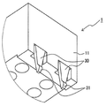
도 1은 경사지게 위에서 본 본 발명의 일 실시예의 커넥터의 사시도이다.
도 2는 경사지게 아래에서 본 도 1의 커넥터의 사시도이다.
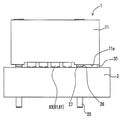
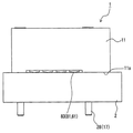
도 3은 도 1에 도시된 커넥터가 회로 기판에 부착되어 있는 상태를 도시하는 사시도이다.
도 4는 도 1의 이중 단차 리벳의 사시도이다.
도 5는 커넥터가 제2 위치(이동 위치)에 있고, 이중 단차 리벳들 각각이 그 단부 부분까지 삽입되어 있는 상태의, 도 1의 회로 기판과 커넥터의 단면도이다.
도 6은 도 5에 도시된 제2 위치에 커넥터가 존재하는 상태의, 도 1에 도시된 회로 기판과 커넥터의 정면도이다.
도 7은 이중 단차 리벳들 각각이 그 경사 부분까지 삽입되어 있는 상태의, 도 1의 회로 기판 및 커넥터의 단면도이다.
도 8은 도 1에 도시된 회로 기판 및 커넥터의 도 7에 도시된 상태의, 정면도이다.
도 9는 커넥터가 부착 위치에 있고, 이중 단차 리벳들 각각이 그 루트 부분까지 삽입되어 있는 상태의, 도 1에 도시된 회로 기판과 커넥터의 단면도이다.
도 10은 커넥터가 도 9에 도시된 부착 위치에 있는 상태의, 도 1에 도시되 s회로 기판과 커넥터의 정면도이다.
도 11은 도 1의 커넥터의 변형례를 도시하는 사시도이다.
도 12는 도 1에 도시된 커넥터의 동축 단자의 제1 변형례를 도시하는 개략도이다.
도 13은 도 1에 도시된 커넥터의 동축 단자의 제2 변형례를 도시하는 개략도이다.
도 14는 도 1에 도시된 커넥터의 동축 단자의 제3 변형례를 도시하는 개략도이다.
도 15는 도 1에 도시된 커넥터의 동축 단자의 제4 변형례를 도시하는 개략도이다.
도 16은 도 1에 도시된 커넥터의 동축 단자의 제5 변형례를 도시하는 개략도이다.
도 17은 종래 기술의 동축 가동 접촉 프로브의 단면도이다.
도 18은 도 17에 도시된 동축 가동 접촉 프로브가 사용중인 상태를 도시하는 도면이다.1 is a perspective view of a connector of one embodiment of the present invention as viewed obliquely from above;
FIG. 2 is a perspective view of the connector of FIG. 1 seen obliquely from below. FIG.
3 is a perspective view showing a state in which the connector shown in FIG. 1 is attached to a circuit board.
4 is a perspective view of the double step rivet of FIG. 1.
5 is a cross-sectional view of the circuit board and connector of FIG. 1 with the connector in the second position (moving position) and with each of the double stepped rivets inserted to its end portion.
FIG. 6 is a front view of the circuit board and the connector shown in FIG. 1, with the connector present in the second position shown in FIG.
FIG. 7 is a cross-sectional view of the circuit board and connector of FIG. 1 with each of the double stepped rivets inserted to its sloped portion. FIG.
FIG. 8 is a front view of the circuit board and connector shown in FIG. 1, shown in FIG. 7.
FIG. 9 is a cross-sectional view of the circuit board and connector shown in FIG. 1 with the connector in the attachment position, with each of the double stepped rivets inserted into its root portion.
10 is a front view of the s circuit board and connector shown in FIG. 1 with the connector in the attachment position shown in FIG.
11 is a perspective view illustrating a modification of the connector of FIG. 1.
12 is a schematic diagram illustrating a first modification of the coaxial terminal of the connector illustrated in FIG. 1.
FIG. 13 is a schematic diagram illustrating a second modification of the coaxial terminal of the connector illustrated in FIG. 1.
14 is a schematic diagram illustrating a third modification example of the coaxial terminal of the connector illustrated in FIG. 1.
FIG. 15 is a schematic diagram illustrating a fourth modification of the coaxial terminal of the connector illustrated in FIG. 1.
16 is a schematic diagram illustrating a fifth modification example of the coaxial terminal of the connector illustrated in FIG. 1.
17 is a cross-sectional view of a coaxial movable contact probe of the prior art.
18 is a view showing a state in which the coaxial movable contact probe shown in FIG. 17 is in use.
이하에서, 도면들을 참조로 본 발명의 커넥터의 일 실시예가 설명될 것이다. 후술된 실시예는 양호한 실시예의 일 예이며, 본 발명을 제한하지 않는다는 것을 이해하여야 한다.In the following, an embodiment of the connector of the present invention will be described with reference to the drawings. It is to be understood that the embodiments described below are examples of preferred embodiments and do not limit the invention.
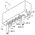
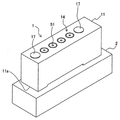
도 1 및 도 2는 본 실시예의 커넥터(1)를 각각 도시하는 도면이다. 도 1은 경사지게 위로부터 본 커넥터(1)의 사시도이고, 도 2는 경사지게 아래로부터 본 커넥터(1)의 사시도이다. 또한, 도 1은 커넥터(1)가 부착되어 있는 회로 기판(2)을 도시한다. 도 3은 커넥터(1)가 회로 기판(2)에 부착되어 있는 상태를 도시하는 사시도이다.1 and 2 are diagrams respectively showing the
도 1에 도시된 바와 같이, 복수의 랜드부들(151)은 랜드부 열들이 각각 랜드부(151)의 3개 조각들로 형성되도록 회로 기판(2) 상에 정렬되어 있다. 관통 구멍들(미도시) 같은 전기 배선들이 랜드부 열들 각각을 형성하도록 정렬되어 있는 세 개의 랜드부들(151)에 연결되어 있다. 이들 이외에, 세 개의 관통 구멍들(111)(관통 구멍(111a) 및 두 개의 관통 구멍들(111b))이 회로 기판(2)에 형성되어 있다.As shown in FIG. 1, the plurality of
커넥터(1)는 수지 같은 절연 재료를 구비하는, 한 방향으로 긴 판 형상을 갖도록 형성된 하우징(11)을 포함한다. 도 1에 도시된 바와 같이, 하우징(11)에는 네 개의 공동들(15) 및 두 개의 리벳 구멍들(29)이 상하 방향으로 하우징(11)을 관통하는 실질적으로 기둥형인 구멍들로서 형성되어 있다. 네 개의 공동들(14)은 하우징(11)의 길이 방향으로 하나의 열로 배열되어 있다. 두 개의 리벳 구멍들(29)은 네 개의 공동들(14)을 그 사이에 개재하도록 배열되어 있다.The
도 2에 도시된 바와 같이, 탄성 아암(30)이 하우징(11)의 길이 방향(도 2의 우측 부분)으로 일 단부 상에 형성되어 있다. 탄성 아암(30)은 하우징(11)의 하부 표면(11a)으로부터 하향 돌출하면서 실질적 판 형상을 갖는다. 또한, 탄성 아암(30)은 하부 표면(11a)으로부터 돌출하는 부분에서 탄성 아암(30)의 외부 표면(도 2의 우측 표면) 상에 형성되어 있는 아암 돌출부(31)를 구비한다. 탄성 아암(30)과 아암 돌출부(31)는 하우징(11)을 형성하는 재료와 동일한 절연 수지 재료를 사용하여 하우징(11)과 일체로 형성된다. 따라서, 도 2에 도시된 상태에서, 아암 돌출부(31)에 좌향력이 인가될 때, 판형 탄성 아암(30)이 좌향 굴곡된다. 탄성 아암(30)은 커넥터(1)의 단면도인 도 5(후술됨)에 도시된 바와 같이, 회로 기판(2)의 관통 구멍(111a) 내에 삽입된다. 또한, 탄성 아암(30)이 관통 구멍(111a) 내에 삽입된 상태에서, 아암 돌출부(31)는 관통 구멍(111a) 내의 회로 기판(2)의 측부 표면 상에 접촉할 수 있다As shown in FIG. 2, an
도 1에 도시된 바와 같이, 이중 단차 리벳들(17)이 각각 리벳 구멍들(29) 내에 삽입된다(가압 끼워맞춤). 도 4에 도시된 바와 같이, 이중 단차 리벳들(17) 각각은 리벳 구멍(29)의 구멍 크기와 실질적으로 동일한 외경을 가지면서 리벳 구멍(29)보다 긴 기둥 형상을 갖는 루트 부분(26)과, 루트 부분(26)으로부터 연장하도록 형성되고 루트 부분(26)보다 얇은 기둥 형상을 갖는 단부 부분(28) 및 루트 부분(26)과 단부 부분(28) 사이에서 이중 단차 리벳(17)의 직경이 매끄럽게 변하도록 루트 부분(26)과 단부 부분(28) 사이에 형성되어 있는 경사 부분(27)을 포함한다. 리벳 구멍들(29) 내에 삽입된 이중 단차 리벳들(17)은 도 2에 도시된 바와 같이, 하우징(11)의 하부 표면(11a)(그를 통해 커넥터(1)가 회로 기판(2)에 부착되는 부착면)으로부터 하향 돌출한다. 구체적으로, 이중 단차 리벳들(17) 각각의 루트 부분(26)의 일부, 경사 부분(27) 및 단부 부분(28)은 하부 표면(11a)으로부터 돌출한다. 이중 단차 리벳들(17)은 도 5(후술됨)에 도시된 바와 같이 회로 기판(2)의 관통 구멍들(111b) 내에 삽입된다.As shown in Fig. 1, double step rivets 17 are inserted into each of the rivet holes 29 (press fit). As shown in FIG. 4, each of the stepped rivets 17 has a
도 1에 도시된 바와 같이, 동축 단자들(51)은 공동들(14) 내에 삽입된다(가압 끼워맞춤). 도 5(후술됨)에 도시된 바와 같이, 동축 단자들(51) 각각은 중앙 단자(52)와 외부 단자(61)로 구성된 동축 구조를 갖는다. 이들 이외에, 동축 단자들(51) 각각은 절연체(41)를 가지며, 이 절연체에 의해 중앙 단자(52)가 절연된 상태로 외부 단자(61)에 의해 보유된다.As shown in FIG. 1, the
중앙 단자(52)는 중앙 전도체(53), 중앙 코일 스프링(58) 및 샤프트형 접촉부(59)를 포함하며, 이들 각각은 전도성 재료를 사용하여 형성된다. 중앙 전도체(53)는 실질적으로 샤프트 형상을 가지며, 그 상부 부분 상에, 동축 플러그(미도시)의 축방향 단자를 보유 또는 개재하는 정합 부분(55)을 갖는다. 또한, 중앙 구멍(56)은 샤프트 형상을 갖는 중앙 전도체(53)의 하부 표면에 형성되고, 중앙 코일 스프링(58) 및 샤프트형 접촉부(59)의 일 단부는 중앙 구멍(56)으로부터 빠져 나오거나 탈락하지 않도록 중앙 구멍(56) 내에 삽입된다.The
외부 단자(61)는 외부 전도체(62), 외부 코일 스프링(71) 및 원통형 접촉부(81)를 포함하며, 이들 각각은 금속 같은 전도성 재료를 사용하여 형성된다. 외부 전도체(62)는 실질적 원통형 형상을 갖는 본체 부분(64)과, 본체 부분(64) 위에 형성된 정합 부분(66)을 포함한다. 정합 부분(66)은 정합 부분(66)이 동축 플러그(미도시)의 주변 단자를 보유 또는 개재하는 구조를 갖는다. 외부 코일 스프링(71) 및 원통형 형상을 갖는 원통형 접촉부(81)의 일 단부는 본체 부분(64)으로부터 빠져 나오거나 탈락하지 않도록 본체 부분(64) 내에 삽입된다.The
절연체(41)는 실질적으로 원통형 형상을 갖는다. 원통형 절연체(41)의 중앙에는 원통형 절연체(41)와 동축으로 중앙 구멍(42)이 형성되며, 중앙 단자(52)가 중앙 구멍(42) 내에 삽입(가압 끼워맞춤)된다. 또한, 절연체(41)는 외부 단자(61)의 본체 부분(64) 내에 삽입(가압 끼워맞춤)된다. 따라서, 중앙 단자(52) 및 외부 단자(61)는 동축으로 배열된다.The
이런 방식으로 형성된 동축 단자들(51)이 하우징(11)의 공동들(14) 내에 삽입(가압 끼워맞춤)된다. 또한, 도 2에 도시된 바와 같이, 외부 단자들(61)의 원통형 접촉부들(81) 각각의 하부 단부와, 중앙 단자들(52)의 샤프트형 접촉부들(59) 각각의 하부 단부는 하우징(11)의 하부 표면(11a)으로부터 돌출한다. 하우징(11)의 하부 표면(11a)으로부터 돌출하는 샤프트형 접촉부(59) 및 원통형 접촉부들(81) 각각의 두 개의 돌출 접촉 지점들(83)은 도 1의 회로 기판(2) 상에 배열되어 있는 세 개의 랜드부들(151)의 세트와 접촉하게 된다.
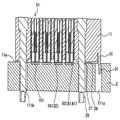
다음에, 커넥터(1)가 회로 기판(2)에 부착되는 방식에 대한 설명이 도 5 내지 도 10을 참조로 제공될 것이다. 도 5 및 도 6은 이중 단차 리벳들(17)의 단부 부분들(28)이 회로 기판(2)의 구멍들(111b) 내에 삽입되어 있는 상태를 각각 도시하는 단면도 및 정면도이다. 도 7 및 도 8은 각각 단면도 및 정면도이며, 이들 각각은 이중 단차 리벳들(17)의 단부 부분들(28) 및 경사 부분들(27)이 회로 기판(2)의 구멍들(111b) 내에 삽입되어 있는 상태를 도시한다. 도 9 및 도 10은 각각 단면도 및 정면도이며, 이들 각각은 하우징(11)의 하부 표면(11a)이 회로 기판(2)과 접촉하는 상태를 도시한다. 커넥터(1)는 도 9 및 도 10에 도시된 상태에서, 회로 기판(2)에 부착된다. 도 5 및 도 6, 도 7 및 도 8, 그리고, 도 9 및 도 10에 도시된 것들 사이의 회로 기판에 대한 커넥터(1)의 위치를 비교하면, 도 7 및 도 8에 도시된 커넥터(1)의 위치는 도 9 및 도 10에 도시된 커넥터(1)의 위치로부터 좌향 이동되고, 도 5 및 도 6에 도시된 커넥터(1)의 위치는 도 7 및 도 8에 도시된 커넥터(1)의 위치로부터 좌향 이동된다. 이하에서, 도 5 및 도 6의 위치는 "제2 위치"라 지칭되며, 도 9 및 도 10의 위치는 "부착 위치"(제1 위치)라 지칭된다.Next, a description of how the
도 5 및 도 6에 도시된 바와 같이, 커넥터(1)에서, 회로 기판(2)에 부착되기 이전에, 동축 단자들(51) 각각의 원통형 접촉부(81)와 샤프트형 접촉부(59)는 하우징(11)의 하부 표면(11a)(커넥터(1)를 회로 기판(2)에 부착시키는 부착 표면)으로부터 돌출한다. 와이핑을 위해, 원통형 접촉부들(81) 각각이 서로 대면하는 돌출 접촉 지점들(83)의 쌍의 하부 단부들과, 원통형 접촉부들(59) 각각의 하부 단부가 이중 단차 리벳들(17) 각각의 루트 부분(26)보다 낮은 위치로 돌출하는 것으로 충분하다는 것을 주의하여야 한다.As shown in FIGS. 5 and 6, in the
커넥터(1)를 회로 기판(2)에 부착할 때, 먼저, 이중 단차 리벳들(17)의 단부 부분들(28)과 탄성 아암(30)이 회로 기판(2)의 구멍들(111b) 및 구멍(11a)과 각각 정렬되고 그에 삽입된다. 여기서, 커넥터(1)는 도 5 및 도 6에 도시된 바와 같이 제2 위치에 위치된다. 또한, 도 5에 도시된 바와 같이, 이중 단차 리벳들(17)의 단부 부분들(28)과 탄성 아암(30)의 하부 단부 부분은 회로 기판(2)의 구멍들(111b) 및 구멍(111a) 내에 삽입되고, 원통형 접촉부들(81)의 돌출 접촉 지점들(83)의 쌍들 및 샤프트형 접촉부들(59)은 회로 기판(2)의 랜드부들(151)과 접촉하게 된다. 또한, 비록, 아암 돌출부(31)가 회로 기판(2)의 구멍(111a) 내에서 회로 기판(2)의 측부 표면과 접촉하지만, 탄성 아암(30)은 실질적으로 직선형 상태(낮은 편향력을 가짐)이다.When attaching the
커넥터(1)를 제2 위치에 배치한 이후, 하우징(11)은 회로 기판(2)에 대해(그에 관하여) 가압된다. 이렇게 함으로써, 이중 단차 리벳들(17)과 탄성 아암(30)은 회로 기판(2)의 구멍들(111b) 및 구멍(111a) 내로 각각 추가로 삽입된다. 이때, 이중 단차 리벳들(17)이 경사 부분들(27)의 존재에 기인하여, 회로 기판(2)의 구멍들(111b)의 개방 에지들을 따라 활주 이동하기 때문에, 하우징(11)은 회로 기판(2)의 표면을 따라(그 위에서) 도 5의 우향으로 이동된다. 또한, 하우징(11)이 회로 기판(2)의 표면 상에서 강제로 이동되기 때문에, 아암 돌출부(31)는 회로 기판(2)의 구멍(111a) 내에서 회로 기판(2)에 대해 가압되며, 그에 의해, 탄성 아암(30)을 굴곡시킨다. 그후, 도 7 및 도 8에 도시된 바와 같이, 이중 단차 리벳들(17)의 경사 부분들(27)이 회로 기판(2)의 구멍들(111b) 내에 삽입된다.After placing the
하우징(11)이 회로 기판(2)에 관하여 더더욱 가압될 때, 이중 단차 리벳들(17) 및 탄성 아암(30)은 회로 기판(2)의 구멍들(111b) 및 구멍(111a) 내로 각각 더더욱 삽입되며, 따라서, 하우징(11)의 하부 표면(11a)이 도 9 및 도 10에 도시된 바와 같이 회로 기판(2) 상에 접촉한다. 여기서, 하우징(11)은 미리 정해진 부착 위치에 위치된다. 또한, 이중 단차 리벳들(17)은 이중 단차 리벳들(17)의 루트 부분들(26)까지 회로 기판(2)의 구멍들(111b) 내에 삽입된다. 또한, 탄성 아암(30)은 크게 굴곡되어 높은 편향력으로 아암 돌출부(31)를 회로 기판(2)을 향해 편향시키며, 이 편향력은 각각 루트 부분들(26) 상에 접하는 관통 구멍들(111b)의 측부 표면들과 루트 부분들(26)에 의해 수용된다. 따라서, 커넥터(1)는 탄성 아암(30)의 편향력에 의해, 그리고, 편향력에 저항하는 루트 부분들(26)에 의해 고정되고, 따라서, 커넥터(1)가 회로 기판(2)에 부착된다.When the
일련의 부착 작업 동안, 도 5에 도시된 이동 위치(제2 위치)에서 돌출 접촉 지점들(83)의 쌍들과 샤프트형 접촉부들(59)은 회로 기판(2)의 랜드부들(151)에 대해 가압되며, 또한, 도 5에 도시된 제2 위치로부터 도 9에 도시된 부착 위치로 회로 기판(2)의 표면 상에서 하우징(11)과 함께 이동된다. 즉, 돌출 접촉 지점들(83)의 쌍들과 샤프트형 접촉부들(59)은 랜드부들(151) 상에서 이동됨으로써, 랜드부들(151)에 대해 가압된 상태를 유지하면서 랜드부들(151)에 대해 문지른다(그 위에서 활주된다). 결과적으로, 돌출 접촉 지점들(83)의 쌍들, 샤프트형 접촉부들(59) 및 랜드부들(151)의 표면들 상의 산화물 필름을 박리 또는 제거하는 것이 가능하며, 랜드부들(151)과 돌출 접촉 지점들(83)의 쌍들 및 원통형 접촉부들(59) 사이에 포획된 먼지를 제거할 수 있다.During the series of attachment operations, the pair of protruding contact points 83 and the shaft-
이 방식으로, 커넥터(1)를 회로 기판(2)에 부착한 이후, 예시되지 않은 플러그들이 커넥터(1)에 부착된다. 플러그들은 각각의 축방향 단자 및 주변 단자가 동축인 동축 플러그를 포함한다. 그후, 플러그들의 축방향 단자들은 커넥터(1)의 중앙 전도체들(53)의 정합 부분들(55) 내에 각각 삽입되고, 플러그들의 주변 단자들은 커넥터(1)의 외부 전도체들(62)의 정합 부분들(66) 내에 각각 삽입된다. 여기서, 동축 플러그들의 축방향 단자들은 중앙 단자들(52)을 통해 회로 기판(2)의 랜드부들(151)에 전기적으로 연결되고, 주변 단자들은 외부 단자들(61)에 의해 회로 기판(2)의 랜드부들(151)에 전기적으로 연결된다.In this way, after attaching the
본 실시예의 커넥터(1)에서, 전술한 바와 같이, 도 5에 도시된 바와 같은 제2 위치에 위치된 하우징(11)은 회로 기판(2)에 대해 가압됨으로써 경사 부분들(27)을 통해 회로 기판(2) 상에서 하우징(11)을 이동시키며, 도 5에 도시된 제2 위치에서 회로 기판(2)의 랜드부들(151)과 접촉하는, 돌출 접촉 지점들(83)과 샤프트형 접촉부들(59)이 랜드부들(151)에 대해 문질러지게 한다. 이는 돌출 접촉 지점들(83)의 쌍들, 샤프트형 접촉부들(59) 및 랜드부들(151)을 위한 와이핑을 수행할 수 있게 한다.In the
상술한 바와 같이, 본 실시예의 커넥터(1)에서, 커넥터(1)가 동축 단자들(51)인 경우에도 커넥터(1)를 회로 기판(2)에 부착할 때 와이핑이 수행될 수 있다. 와이핑에 의해, 돌출 접촉 지점들(83)의 쌍들, 샤프트형 접촉부들(59) 및 랜드부들(151)의 표면들로부터 산화물 필름을 문질러 벗겨낼 수 있고, 그 사이에 포획된 먼지를 제거할 수 있으므로, 동축 단자들(51)과 랜드부들(151) 사이의 연결 신뢰성의 개선을 보증할 수 있다.As described above, in the
또한, 도 5에 도시된 제2 위치로부터 도 9에 도시된 부착 위치로의 하우징(11)의 이동 동안, 원통형 접촉부들(81)의 돌출 접촉 지점들(83)의 쌍들 및 샤프트형 접촉부들(59)은 외부 코일 스프링들(71) 및 중앙 코일 스프링들(58)의 편향력들에 의해 회로 기판(2)의 랜드부들(151)을 향해 편향되며, 편향된 상태 하에서 와이핑이 수행될 수 있다. 따라서, 예로서, 원통형 접촉부들(81)과 샤프트형 접촉부들(59)이 하우징(11)에 고정되는 경우에 발생하는 비균일 정렬에 기인하여, 동축 단자들(51)의 돌출 접촉 지점들(83)의 쌍들 중 일부와 원통형 접촉부들(59) 중 일부가 임의의 과도하게 높은 편향력에 의해 랜드부들(151)에 대해 편향되거나 단자들(51) 중 단지 일부만이 랜드부들(151)로 편향되는 것 같은 상황이 발생하지 않는다. 따라서, 회로 기판(2)의 랜드부들(151)이 손상되지 않는다. 또한, 커넥터(1)의 단자들이 동축 단자들(51)이기 때문에, 단자들 사이의 누화를 억제할 수 있다. 결과적으로, 본 커넥터(1)에서, 신호의 고주파수 성분을 전송하기에 충분한 성능이 달성될 수 있다. 따라서, 커넥터(1)는 어떠한 납땜도 없이 동축 케이블들을 사용하여 신호 발생기 회로, 비교기 등이 그 위에 장착되어 있는 측정 회로 기판에 대해 측정 타겟이 그 위에 장착되어 있는 회로 기판을 연결하기 위해 사용될 수 있다.Further, during the movement of the
본 실시예에서, 탄성 아암(30)의 하나의 조각은 도 2에 도시된 바와 같이 하우징(11)의 일 단부 부분 상에 형성된다는 것을 주의하여야 한다. 이렇지 않으면, 도 11에 도시된 바와 같이, 탄성 아암(30)의 두 개의 조각을 하우징(11) 상에 형성하는 것도 허용된다. 또한, 비록 두 개의 이중 단차 리벳(17)이 하우징(11)상에 제공되어 있지만, 한 조각의 이중 단차 리벳(17)을 제공하는 것이나, 하우징(11) 상에 셋 이상의 이중 단차 리벳(17)을 제공하는 것도 허용된다.It should be noted that in this embodiment, one piece of
또한, 본 실시예에서, 루트 부분(26)과 경사 부분(27)과 단부 부분(28)을 각각 갖는 이중 단차 리벳들(17)이 사용되어 경사 부분들(27)이 회로 기판(2)의 구멍들(111b)의 개방 에지들에 대해 문질러지는 경사면들로서 기능함으로써 도 5에 도시된 바와 같은 제2 위치(이동 위치)로부터 도 9에 도시된 바와 같은 부착 위치로 하우징(11)을 이동시킨다. 대안적으로, 예로서, 각각 원통형 형상을 가지면서 단부 부분이 경사지게 절단되어 있는 일반적 유형의 리벳들을 사용하고, 일반적 유형의 리벳들의 단부 부분들을 경사지게 절단함으로써 형성된 경사면들을 통해(그에 의해) 제2 위치(이동 위치)로부터 부착 위치로 하우징(11)을 이동시키는 것도 가능하다.In addition, in the present embodiment, double step rivets 17 each having a
또한, 본 실시예에서, 도 2에 도시된 바와 같이, 탄성 아암(30)은 판 형상을 가지며, 아암 돌출부(31)는 일 방향으로 탄성 아암(30)의 외부면으로부터 돌출한다. 그 이외에, 예로서, 탄성 아암(30)은 기둥 형상으로 형성되고, 아암 돌출부(31)는 탄성 아암(30)의 전체 주연부 상에서 돌출할 수 있다. 대안적으로, 탄성 아암(30)은 하우징(11)과 별개로 형성된 부재일 수 있으며, 또한, 금속 재료로 이루어질 수 있다. 즉, 탄성 아암(30)은 탄성 아암(30)이 도 2의 좌향 방향으로 힘을 인가할 수 있다면 임의의 형태로 제공될 수 있다.Also, in the present embodiment, as shown in FIG. 2, the
또한, 본 실시예에서, 탄성 아암(30) 및 이중 단차 리벳들(17)은 하우징(11)의 측부 상에 제공되며, 관통 구멍들(111a, 111b)이 회로 기판(2)에 형성된다. 이들 이외에, 예로서, 탄성 아암(30)과 이중 단차 리벳들(17) 중 적어도 하나가 회로 기판(2)의 측부 상에 제공되고, 이에 대응하는 관통 구멍들(111a, 111b)이 하우징(11) 내에 형성될 수 있다.Also, in this embodiment, the
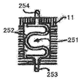
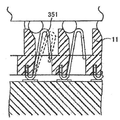
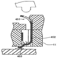
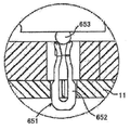
또한, 커넥터 내에 제공된 단자들은 본 실시예에서와 같이 동축 단자들(51)에 한정되지 않으며, 단자들의 형상은 변경될 수 있고, 예로서, 단자는 하나의 부재의 형태일 수 있다. 구체적으로, 예로서, 단자는 스프링 부분(252)과 스프링 부분(252)의 위 및 아래에 형성된 단자 부분들(253, 254)의 쌍을 갖는 형상을 얻도록 한 장의 금속 판에 프레스 가공을 수행하여 형성되는 도 12에 도시된 바와 같은 단자(251)일 수 있거나, 단자는 실질적 S 형상을 갖도록 한 장의 금속판을 굴곡시킴으로써 형성되는 도 13에 도시된 단자(351)일 수 있거나, C 형 부분(452)과 다리 부분(453)을 갖는 형상을 얻도록 한 장의 금속 판을 굴곡시킴으로써 형성된 도 14에 도시된 바와 같은 단자(451)일 수 있다. 대안적으로, 단자는 밀접하게 말려지지 않은(비교적 느슨하게 말려진) 긴 코일 스프링의 중앙 부분(552)으로 형성된 도 15에 도시된 바와 같은 단자(551)일 수 있다. 또한, 대안적으로, 단자는 실질적 U 형상을 가지면서 금속 볼(653)이 금속 판(652) 상에 배치되어 있는 금속 판(652)으로 구성된 도 6에 도시된 바와 같은 단자(651)일 수 있다. 단자들이 주로 상향 및 하향으로 이동하는 단자들(251, 351, 451, 551, 651)인 경우에도 본 발명이 적용되어 커넥터 부착시 와이핑을 수행하고, 따라서, 본 실시예에서와 유사한 방식으로 연결 신뢰성을 향상시킬 수 있다.Further, the terminals provided in the connector are not limited to the
본 발명의 커넥터를 회로 기판에 부착할 때, 랜드부들에 대해 단자들을 문지름으로써 와이핑을 수행하는 것이 가능하다. 따라서, 단자들이 각각 동축 구조를 가지는 단자들이거나 단일 부재로 형성되는 경우에도 커넥터 부착시 와이핑을 수행할 수 있으며, 따라서, 단자와 랜드부들을 연결 신뢰성을 저하시키지 않고 전기적으로 연결할 수 있다. 따라서, 본 발명의 커넥터는 예로서, 케이블들, 회로 기판 등으로, 신호 발생기 회로, 비교기 등이 장착되어 있는 측정 회로 기판과 측정 타겟이 장착되어 있는 회로 기판을 연결하기 위해 예로서 측정 장치 등에서 커넥터로서 사용될 수 있다.When attaching the connector of the present invention to a circuit board, it is possible to perform wiping by rubbing the terminals against the land portions. Therefore, even when the terminals are coaxial structures or formed as a single member, the wiping can be performed when the connector is attached, and thus the terminals and the land portions can be electrically connected without degrading the connection reliability. Accordingly, the connector of the present invention is, for example, a cable, a circuit board, or the like, for example, a connector in a measuring device or the like for connecting a measurement circuit board on which a signal generator circuit, a comparator, etc. is mounted, and a circuit board on which a measurement target is mounted. Can be used as.
Claims (7)
상기 회로 기판의 미리 정해진 부착 위치에서 상기 회로 기판에 부착되는 하우징과,
상기 하우징으로부터 돌출하여 상기 랜드부와 접촉하게 되는 단자와,
상기 회로 기판에 대해 상기 커넥터를 부착하기 위해 상기 단자가 상기 랜드부와 접촉하게 될 때, 상기 부착 위치로부터 이동된 이동 위치에서 상기 회로기판 상에 상기 하우징을 배치하는 메커니즘을 포함하고,
상기 단자는 상기 하우징이 상기 이동 위치로부터 상기 부착 위치로 활주 이동하는 동안 상기 랜드부를 문지르는 것을 특징으로 하는 커넥터.A connector attached to a circuit board having a land portion,
A housing attached to the circuit board at a predetermined attachment position of the circuit board,
A terminal protruding from the housing and contacting the land portion;
A mechanism for placing the housing on the circuit board at a moving position moved from the attachment position when the terminal comes into contact with the land portion to attach the connector to the circuit board,
And the terminal rubs the land portion while the housing slides from the moving position to the attaching position.
상기 하우징은 상기 탄성 아암이 상기 구멍 내에 삽입될 때 상기 이동 위치에 배치되는 것을 특징으로 하는 커넥터.The apparatus of claim 1, wherein the mechanism includes an elastic arm that protrudes from the housing and is inserted into a hole formed in the circuit board,
And the housing is disposed in the moving position when the elastic arm is inserted into the hole.
Applications Claiming Priority (2)
| Application Number | Priority Date | Filing Date | Title |
|---|---|---|---|
| JP2008328978A JP5258543B2 (en) | 2008-12-25 | 2008-12-25 | connector |
| JPJP-P-2008-328978 | 2008-12-25 |
Publications (1)
| Publication Number | Publication Date |
|---|---|
| KR20110097994A true KR20110097994A (en) | 2011-08-31 |
Family
ID=41728471
Family Applications (1)
| Application Number | Title | Priority Date | Filing Date |
|---|---|---|---|
| KR1020117017199A KR20110097994A (en) | 2008-12-25 | 2009-12-22 | Coaxial connector |
Country Status (4)
| Country | Link |
|---|---|
| JP (1) | JP5258543B2 (en) |
| KR (1) | KR20110097994A (en) |
| CN (1) | CN102326303B (en) |
| WO (1) | WO2010075336A1 (en) |
Families Citing this family (8)
| Publication number | Priority date | Publication date | Assignee | Title |
|---|---|---|---|---|
| JP2014093198A (en) * | 2012-11-02 | 2014-05-19 | Yazaki Corp | Connector device with lever |
| WO2014132274A1 (en) * | 2013-02-27 | 2014-09-04 | Power-One Italy S.P.A. | Programming connector |
| KR101548572B1 (en) * | 2014-05-07 | 2015-09-01 | 주식회사 쏠리드 | Flowable coupled device of connector |
| CN108432053B (en) | 2016-01-18 | 2020-08-18 | 胡贝尔舒纳公司 | Board connector assembly, connector and method of forming board connector assembly |
| CN110323608A (en) * | 2018-03-30 | 2019-10-11 | 泰科电子(上海)有限公司 | The pedestal of connector mould group and connector mould group |
| CN108448278A (en) * | 2018-05-18 | 2018-08-24 | 吴通控股集团股份有限公司 | A kind of frame-type connection structure |
| CN111162419B (en) * | 2018-11-08 | 2022-07-12 | 上海雷迪埃电子有限公司 | Radio frequency connector and radio frequency connection structure between two circuit boards |
| US11936145B2 (en) | 2022-01-04 | 2024-03-19 | Te Connectivity Solutions Gmbh | Controlled impedance compressible connector |
Family Cites Families (8)
| Publication number | Priority date | Publication date | Assignee | Title |
|---|---|---|---|---|
| JPS60123666U (en) | 1984-01-30 | 1985-08-20 | 株式会社ヨコオ | Inspection equipment for circuit boards, etc. |
| JPH07272810A (en) | 1994-03-31 | 1995-10-20 | Enplas Corp | Movable contact pin device for ic socket |
| US5936421A (en) * | 1994-10-11 | 1999-08-10 | Virginia Panel Corporation | Coaxial double-headed spring contact probe assembly and coaxial surface contact for engagement therewith |
| JPH10302914A (en) * | 1997-04-25 | 1998-11-13 | Amp Japan Ltd | Electric connector |
| US5938451A (en) * | 1997-05-06 | 1999-08-17 | Gryphics, Inc. | Electrical connector with multiple modes of compliance |
| US6234820B1 (en) * | 1997-07-21 | 2001-05-22 | Rambus Inc. | Method and apparatus for joining printed circuit boards |
| FR2827085B1 (en) * | 2001-07-05 | 2004-01-30 | Cinch Connecteurs Sa | ELECTRIC CONTACT MEMBER FOR COOPERATING WITH AN ELECTRIC CIRCUIT PLOT AND HOUSING FOR RECEIVING SUCH AN ORGAN |
| WO2008114350A1 (en) * | 2007-03-16 | 2008-09-25 | Fujitsu Limited | Connection module |
-
2008
- 2008-12-25 JP JP2008328978A patent/JP5258543B2/en not_active Expired - Fee Related
-
2009
- 2009-12-22 CN CN200980157386.4A patent/CN102326303B/en not_active Expired - Fee Related
- 2009-12-22 KR KR1020117017199A patent/KR20110097994A/en not_active Application Discontinuation
- 2009-12-22 WO PCT/US2009/069110 patent/WO2010075336A1/en active Application Filing
Also Published As
| Publication number | Publication date |
|---|---|
| JP2010153156A (en) | 2010-07-08 |
| WO2010075336A1 (en) | 2010-07-01 |
| JP5258543B2 (en) | 2013-08-07 |
| CN102326303A (en) | 2012-01-18 |
| CN102326303B (en) | 2014-03-12 |
Similar Documents
| Publication | Publication Date | Title |
|---|---|---|
| KR20110097994A (en) | Coaxial connector | |
| KR101235936B1 (en) | Coaxial connector | |
| US8333595B2 (en) | Coaxial connector | |
| JP5352525B2 (en) | Probe pin contact, probe pin, and connection jig for electronic devices | |
| US8011939B2 (en) | Coaxial connector | |
| US9140722B2 (en) | Contact and connector | |
| JP4614434B2 (en) | probe | |
| JP2007017234A (en) | Socket for inspection device | |
| JP5008582B2 (en) | Contact probe | |
| WO2015041099A1 (en) | Contact pin and electrical component socket | |
| KR20110097995A (en) | Coaxial connector | |
| US20210359439A1 (en) | Electrical connector and method of inspecting the electrical connector | |
| CN212849122U (en) | Detection connector | |
| KR20060052128A (en) | Cable connector | |
| JP2011198627A (en) | Coaxial connector with switch | |
| KR100719428B1 (en) | Contact pin, contact pin assembly and socket for electric parts | |
| JPH09219267A (en) | Bga-ic package testing contact socket | |
| KR20210132709A (en) | Electrical Contacts and Electrical Connections | |
| JP5125854B2 (en) | Probing socket | |
| KR101706205B1 (en) | Contactor for testing a semiconductor device and test socket including the same | |
| JP2000180470A (en) | Probe for inspection | |
| JP2005156450A (en) | Probe | |
| JP2005274303A (en) | Characteristic impedance measuring tool | |
| JPH0718273U (en) | Measurement connector | |
| JP2005156313A (en) | Probe |
Legal Events
| Date | Code | Title | Description |
|---|---|---|---|
| A201 | Request for examination | ||
| E902 | Notification of reason for refusal | ||
| E601 | Decision to refuse application |