KR20110013289A - Light emitting device, display device, and method of manufacturing light emitting device - Google Patents
Light emitting device, display device, and method of manufacturing light emitting device Download PDFInfo
- Publication number
- KR20110013289A KR20110013289A KR1020100073124A KR20100073124A KR20110013289A KR 20110013289 A KR20110013289 A KR 20110013289A KR 1020100073124 A KR1020100073124 A KR 1020100073124A KR 20100073124 A KR20100073124 A KR 20100073124A KR 20110013289 A KR20110013289 A KR 20110013289A
- Authority
- KR
- South Korea
- Prior art keywords
- light emitting
- partition wall
- partition
- liquid
- substrate
- Prior art date
Links
Images


Classifications
-
- H—ELECTRICITY
- H10—SEMICONDUCTOR DEVICES; ELECTRIC SOLID-STATE DEVICES NOT OTHERWISE PROVIDED FOR
- H10K—ORGANIC ELECTRIC SOLID-STATE DEVICES
- H10K59/00—Integrated devices, or assemblies of multiple devices, comprising at least one organic light-emitting element covered by group H10K50/00
- H10K59/10—OLED displays
- H10K59/12—Active-matrix OLED [AMOLED] displays
- H10K59/122—Pixel-defining structures or layers, e.g. banks
-
- H—ELECTRICITY
- H10—SEMICONDUCTOR DEVICES; ELECTRIC SOLID-STATE DEVICES NOT OTHERWISE PROVIDED FOR
- H10K—ORGANIC ELECTRIC SOLID-STATE DEVICES
- H10K59/00—Integrated devices, or assemblies of multiple devices, comprising at least one organic light-emitting element covered by group H10K50/00
- H10K59/30—Devices specially adapted for multicolour light emission
- H10K59/35—Devices specially adapted for multicolour light emission comprising red-green-blue [RGB] subpixels
-
- H—ELECTRICITY
- H10—SEMICONDUCTOR DEVICES; ELECTRIC SOLID-STATE DEVICES NOT OTHERWISE PROVIDED FOR
- H10K—ORGANIC ELECTRIC SOLID-STATE DEVICES
- H10K71/00—Manufacture or treatment specially adapted for the organic devices covered by this subclass
- H10K71/10—Deposition of organic active material
- H10K71/12—Deposition of organic active material using liquid deposition, e.g. spin coating
- H10K71/13—Deposition of organic active material using liquid deposition, e.g. spin coating using printing techniques, e.g. ink-jet printing or screen printing
- H10K71/135—Deposition of organic active material using liquid deposition, e.g. spin coating using printing techniques, e.g. ink-jet printing or screen printing using ink-jet printing
Landscapes
- Engineering & Computer Science (AREA)
- Manufacturing & Machinery (AREA)
- Microelectronics & Electronic Packaging (AREA)
- Electroluminescent Light Sources (AREA)
Abstract
Description
본 발명은 발광장치, 표시장치 및, 발광장치의 제조방법에 관한 것이다.The present invention relates to a light emitting device, a display device, and a manufacturing method of the light emitting device.
발광장치로서는 예를 들면, 유기EL(electroluminescence)소자를 발광소자로서 이용한 발광장치가 있다. 유기EL소자는 애노드 전극과, 캐소드 전극과, 이들의 한 쌍의 전극 사이에 형성되는 유기EL층(발광층)을 구비한다. 1개의 유기EL소자가 1화소가 된다.As a light emitting device, for example, there is a light emitting device using an organic EL (electroluminescence) element as a light emitting element. The organic EL element includes an anode electrode, a cathode electrode, and an organic EL layer (light emitting layer) formed between a pair of these electrodes. One organic EL element becomes one pixel.
상기의 발광층은 예를 들면, 일본국 특개 2002-75640호 공보에 개시되어 있는 바와 같이, 격벽에 의해 간막이된 기판 위의 영역을 덮도록, 복수 화소분, 한번에 형성된다. 여기서, 격벽에 의해 간막이된 기판 위의 영역이란, 즉, 격벽과, 기판에 의해서 형성되는 홈의 저면(底面)이다.Said light emitting layer is formed in several pixels at once, so that the area | region on the board | substrate which was partitioned by the partition can be formed as disclosed, for example in Unexamined-Japanese-Patent No. 2002-75640. Here, the area | region on the board | substrate which was partitioned by the partition wall, ie, the bottom surface of a partition and the groove | channel formed by the board | substrate.
이와 같은 발광층의 제조방법으로서는 예를 들면, 이하와 같은 방법이 있다. 우선, 발광층의 재료를 포함하는 용액(이하에서는, 잉크라고 한다.)을, 격벽과, 복수의 전극(예를 들면, 복수의 애노드 전극 등의 복수의 화소전극)이 형성된 기판에 의해서 형성되는 홈에 도포한다. 잉크의 도포는 잉크젯 프린팅 또는 노즐 프린팅 등에 의해서 실행된다. 그리고, 도포한 잉크를 건조시키는 것에 의해, 격벽과, 기판에 의해서 형성되는 홈의 저면을 덮는 발광층을 형성한다.As a manufacturing method of such a light emitting layer, there exist the following methods, for example. First, a solution containing a material of the light emitting layer (hereinafter referred to as ink) is a groove formed by a partition and a substrate on which a plurality of electrodes (for example, a plurality of pixel electrodes such as a plurality of anode electrodes) are formed. Apply to Application of the ink is performed by ink jet printing or nozzle printing. By drying the applied ink, a partition and a light emitting layer covering the bottom surface of the groove formed by the substrate are formed.
여기서, 발광층은 기판 위의 복수의 전극을 모두 덮도록 형성하는 것이 바람직하다. 그 때문에, 잉크를, 격벽과, 기판에 의해서 형성되는 홈의 저면 전면을 덮도록 도포하고, 이것을 건조시켜, 발광층을 형성하도록 구성된다.Here, the light emitting layer is preferably formed so as to cover all of the plurality of electrodes on the substrate. Therefore, it is comprised so that ink may be apply | coated so that a partition and a whole surface of the bottom face of the groove | channel formed by the board | substrate may be covered, and this is dried and a light emitting layer is formed.
그러나, 본원 발명자는 홈의 저면 전면을 덮도록 잉크를 도포하고, 이것에 의해서 발광층을 형성하도록 해도, 홈의 저면에 있어서 발광층에 의해 덮여지지 않는 영역이 형성되어 버릴 경우가 있다.However, the inventors of the present application apply ink so as to cover the entire bottom surface of the grooves, whereby a region not covered by the light emitting layer may be formed on the bottom surface of the grooves.
또한, 이와 같은 현상은 유기EL소자와 마찬가지의 구성을 갖는 다른 발광소자의 형성에 있어서도 발생할 수 있다고 생각된다.In addition, it is thought that such a phenomenon can also occur in the formation of another light emitting element having the same structure as the organic EL element.
본 발명은 격벽에 의해 간막이된 홈의 저면에 있어서, 상기 발광층에 의해 덮여지지 않는 영역을 없애거나 적게 할 수 있는, 발광장치, 전자기기 및, 발광장치의 제조방법을 제공할 수 있는 이점을 갖는다.The present invention has the advantage of providing a light emitting device, an electronic device, and a manufacturing method of the light emitting device, which can eliminate or reduce the area not covered by the light emitting layer on the bottom surface of the groove partitioned by the partition wall. .
상기 이점을 얻기 위한, 본 발명의 발광장치는,The light emitting device of the present invention to obtain the above advantages,
발광소자를 갖는, 적어도 하나의 화소를 가지고 이루어지는 발광장치로서,A light emitting device having at least one pixel having a light emitting element,
기판과,Substrate,
상기 기판 위에 형성된 격벽과,Barrier ribs formed on the substrate;
상기 격벽에 의해 간막이된 적어도 하나의 홈내에 형성된, 상기 발광소자의 발광층을 구비하고,A light emitting layer of the light emitting element formed in at least one groove partitioned by the partition wall,
상기 격벽은,The partition wall,
제 1 방향으로 연장해서 형성된 복수의 제 1 격벽과,A plurality of first partition walls extending in a first direction,
상기 제 1 방향과 직교하는 제 2 방향으로 연장하며, 상기 복수의 제 1 격벽의 단부끼리를 연결하도록 형성된 적어도 1개의 제 2 격벽을 갖고,Has at least one second partition wall extending in a second direction orthogonal to the first direction and formed to connect end portions of the plurality of first partition walls,
상기 제 2 격벽의 발액도는 각 상기 제 1 격벽의 상기 제 1 방향을 따른 양단 사이의 중앙의 영역의 발액도보다도 낮다.The liquid repellency degree of the said 2nd partition wall is lower than the liquid repellency degree of the center area | region between the both ends along the said 1st direction of each said 1st partition wall.
상기 이점을 얻기 위한, 본 발명의 전자기기는,The electronic device of the present invention for obtaining the above advantages,
조작부와, 표시부를 갖고,Has an operation unit and a display unit,
상기 표시부는 표시 데이터에 따른 화상정보를 표시하는 표시장치를 구비하며,The display unit includes a display device for displaying image information according to display data,
상기 표시장치는,The display device,
기판과,Substrate,
상기 기판 위에 형성된 격벽과,Barrier ribs formed on the substrate;
상기 격벽에 의해 간막이된 적어도 하나의 홈내에 형성된, 발광소자의 발광층을 구비하고,And a light emitting layer of the light emitting element, formed in at least one groove partitioned by the partition wall,
상기 격벽은,The partition wall,
제 1 방향으로 연장해서 형성된 복수의 제 1 격벽과,A plurality of first partition walls extending in a first direction,
상기 제 1 방향과 직교하는 제 2 방향으로 연장하며, 각 상기 제 1 격벽의 단부끼리를 연결하도록 형성된 적어도 1개의 제 2 격벽을 갖고,Has at least one second partition wall extending in a second direction orthogonal to the first direction and formed to connect end portions of the first partition walls,
상기 제 2 격벽의 발액도는 각 상기 제 1 격벽의 상기 제 1 방향을 따른 양단 사이의 중앙의 영역의 발액도보다도 낮다.The liquid repellency degree of the said 2nd partition wall is lower than the liquid repellency degree of the center area | region between the both ends along the said 1st direction of each said 1st partition wall.
상기 이점을 얻기 위한, 본 발명의 발광장치의 제조방법은,In order to obtain the above advantages, the manufacturing method of the light emitting device of the present invention,
발광소자를 갖는, 적어도 하나의 화소를 구비하는 발광장치의 제조방법으로서,A method of manufacturing a light emitting device having at least one pixel having a light emitting element,
기판 위에, 복수의 제 1 격벽을, 제 1 방향으로 연장하며, 상기 발광소자의 발광층의 형성영역을 간막이하도록 형성하고, 적어도 1개의 제 2 격벽을, 상기 제 1 방향과 직교하는 제 2 방향으로 연장하며, 상기 복수의 제 1 격벽의 단부끼리를 연결하도록 형성하는 격벽형성스텝과,On the substrate, a plurality of first partition walls extend in a first direction, so as to partition a region in which a light emitting layer is formed in the light emitting element, and at least one second partition wall in a second direction orthogonal to the first direction. A barrier rib forming step of extending and connecting end portions of the plurality of first barrier ribs;
상기 제 2 격벽의 발액도가 각 상기 제 1 격벽의 상기 제 1 방향을 따른 양단 사이의 중앙의 영역의 발액도보다 낮아지도록, 각 상기 제 1 격벽과 상기 제 2 격벽의 발액도를 조정하는 발액도 조정스텝을 포함한다.Repellent for adjusting the repellency degree of each said 1st partition wall and a said 2nd partition wall so that the repellency degree of the said 2nd partition wall may become lower than the repellency degree of the area | region between the both ends along the said 1st direction of each said 1st partition wall. It also includes a degree adjustment step.
본 발명에 관한 발광장치, 표시장치 및, 발광장치의 제조방법에 따르면, 격벽과, 기판에 의해서 형성되는 홈의 저면에 있어서 발광층에 의해 덮여지지 않는 영역을 없애거나 적게 할 수 있다.According to the light emitting device, the display device, and the manufacturing method of the light emitting device according to the present invention, the area not covered by the light emitting layer on the partition wall and the bottom of the groove formed by the substrate can be eliminated or reduced.
도 1은 본 발명의 한 실시형태에 관한 발광장치의 구성의 개요를 나타내는 도면이다.
도 2는 본 발명의 한 실시형태에 관한 발광장치의 제조방법을 설명하기 위한 흐름도이다.
도 3은 본 발명의 한 실시형태에 관한 발광장치의 제조방법을 설명하기 위한 도면이며, 기판 및 격벽을 형성한 단계에 있어서의 기판 및 격벽을 나타내는 도면이다.
도 4는 도 3에 있어서, 제 1 격벽과, 제 2 격벽의 관계를 나타내는 도면이다.
도 5는 본 발명의 한 실시형태에 관한 발광장치의 제조방법을 설명하기 위한 도면이며, 기판, 격벽 및, 발광층을 형성한 단계에 있어서의 기판, 격벽 및, 발광층을 나타내는 도면이다.
도 6은 본 발명의 한 실시형태에 관한 발광장치의 제조방법을 설명하기 위한 도면이며, 기판, 격벽, 발광층 및, 대향전극을 형성한 단계에 있어서의 기판, 격벽, 발광층 및, 대향전극을 나타내는 도면이다.
도 7a, 도 7b는 도 6에 있어서의 Ⅶ-Ⅶ 개략 단면도이다.
도 8은 도 6에 있어서의 Ⅷ-Ⅷ 개략 단면도이다.
도 9는 본원 발명자가 종래 실행하고 있었던 발광장치의 제조방법으로 형성한 발광층의 형상의 일례를 나타내는 도면이다.
도 10은 도 2의 스텝S103의 제 1 예를 설명하기 위한 흐름도이다.
도 11a, 도 11b는 제 1 예의 친액화 처리의 일례를 설명하기 위한 도면이다.
도 12는 제 1 예의 발액화 처리(lyophobic property vesting process)의 일례를 설명하기 위한 도면이다.
도 13은 제 1 예의 친액화 처리의 일례를 설명하기 위한 도면이다.
도 14는 도 2의 스텝S103의 제 2 예를 설명하기 위한 흐름도이다.
도 15는 제 2 예의 발액화 처리의 일례를 설명하기 위한 도면이다.
도 16은 본 발명의 한 실시형태에 관한 발광장치가 구비하는 발광층의 다른 예를 나타내는 단면도이다.
도 17은 본 발명의 한 실시형태에 관한 발광장치를 표시부에 사용한 디지털 카메라의 도면이다.
도 18은 본 발명의 한 실시형태에 관한 발광장치를 표시부에 사용한 디지털 카메라의 도면이다.
도 19는 본 발명의 한 실시형태에 관한 발광장치를 표시부에 사용한 노트북 컴퓨터의 도면이다.
도 20은 본 발명의 한 실시형태에 관한 발광장치를 표시부에 사용한 휴대전화기의 도면이다.1 is a diagram showing an outline of a configuration of a light emitting device according to an embodiment of the present invention.
2 is a flowchart for explaining a method of manufacturing a light emitting device according to one embodiment of the present invention.
FIG. 3 is a view for explaining a method of manufacturing a light emitting device according to one embodiment of the present invention, which shows the substrate and the partition wall in the step of forming the substrate and the partition wall.
FIG. 4 is a diagram illustrating a relationship between a first partition and a second partition in FIG. 3.
FIG. 5 is a view for explaining a method of manufacturing a light emitting device according to one embodiment of the present invention, which shows a substrate, a partition, and a light emitting layer in the step of forming a substrate, a partition, and a light emitting layer.
Fig. 6 is a view for explaining a method of manufacturing a light emitting device according to one embodiment of the present invention, which shows a substrate, a partition, a light emitting layer, and a counter electrode in the step of forming a substrate, a partition, a light emitting layer, and a counter electrode. Drawing.
7A and 7B are schematic sectional views taken along line VIII-VIII in FIG. 6.
FIG. 8 is a schematic sectional view taken along line VIII of FIG. 6.
Fig. 9 is a diagram showing an example of the shape of the light emitting layer formed by the method of manufacturing a light emitting device which has been conventionally performed by the inventor.
10 is a flowchart for explaining a first example of step S103 of FIG. 2.
11A and 11B are diagrams for explaining an example of the lyophilic treatment of the first example.
12 is a view for explaining an example of a lyophobic property vesting process of the first example.
It is a figure for demonstrating an example of the lyophilic process of a 1st example.
FIG. 14 is a flowchart for explaining a second example of step S103 of FIG. 2.
FIG. 15 is a diagram for explaining an example of the liquid-repellent treatment of the second example.
16 is a cross-sectional view showing another example of the light emitting layer included in the light emitting device according to one embodiment of the present invention.
17 is a diagram of a digital camera using a light emitting device according to an embodiment of the present invention on a display unit.
18 is a diagram of a digital camera using a light emitting device according to an embodiment of the present invention on a display unit.
19 is a diagram of a notebook computer using the light emitting device according to one embodiment of the present invention in a display unit.
20 is a diagram of a mobile telephone using the light emitting device according to one embodiment of the present invention in a display unit.
본 발명의 한 실시형태에 대해 도면을 참조해서 설명한다. 또한, 본 발명은 하기에서 설명하는 실시형태(도면에 기재된 내용도 포함한다.)에 의해서 한정되는 것은 아니다. 하기에서 설명하는 실시형태에 변경을 부가할 수 있다. 하기에서 설명하는 실시형태의 구성요소를 적절히 삭제해도 좋다.One embodiment of this invention is described with reference to drawings. In addition, this invention is not limited by embodiment described below (it also includes the content described in drawing). Modifications can be added to the embodiments described below. You may delete the component of embodiment described below suitably.
또한, 하기에서는 발광소자로서 유기EL소자를 채용한 발광장치(표시장치)에 대해 설명하지만, 본 발명에 관한 발광장치는 유기EL소자 이외의 발광소자를 채용한 것이라도 좋다.In the following, a light emitting device (display device) employing an organic EL element as a light emitting element will be described. However, the light emitting device according to the present invention may employ a light emitting element other than the organic EL element.
우선, 본 실시형태에 관한 발광장치(1)의 구성의 개요에 대해 설명한다.First, the outline | summary of the structure of the light emitting device 1 which concerns on this embodiment is demonstrated.
도 1은 본 발명의 한 실시형태에 관한 발광장치의 구성의 개요를 나타내는 도면이다.1 is a diagram showing an outline of a configuration of a light emitting device according to an embodiment of the present invention.
발광장치(1)는 한면 위에 복수의 화소(PIX)가 배치설치된 표시영역(150)이 형성된 기판(100)을 구비한다. 이 기판(100)은 예를 들면, 복수의 기판(100)이 형성되는 큰 기판을 각기판(100)에 분할해서 형성된 것이다.The light emitting device 1 includes a
도 1에 나타내는 바와 같이, 기판(100)의 일면 위의 표시영역(150)에는 R (적), G(녹), B(청) 중의 어느 하나의 발광색으로 발광하는 발광소자를 구비하는 복수의 화소(PIX)가 매트릭스 형상으로 배치설치되어 있다. 각 화소(PIX)는 R(적)의 발광색으로 발광하는 발광소자를 구비하는 복수의 화소(PIX), G(녹)의 발광색으로 발광하는 발광소자를 구비하는 복수의 화소(PIX), B(청)의 발광색으로 발광하는 발광소자를 구비하는 복수의 화소(PIX)가 각각 열방향을 따라 늘어서서 배열되며, 또한, 행방향을 따라, R(적)의 발광색으로 발광하는 발광소자를 구비하는 화소 (PIX), G(녹)의 발광색으로 발광하는 발광소자를 구비하는 화소(PIX), B(청)의 발광색으로 발광하는 발광소자를 구비하는 화소(PIX)의 순서로 배열되어 있다.As shown in FIG. 1, the
또, 도 1에 나타내는 바와 같이, 기판(100)의 일면 위에는 각 화소(PIX)의 발광소자의 형성영역을 간막이하는 격벽(200)이 형성되어 있다. 이 격벽(200)에 둘러싸인 복수의 영역이, 복수의 화소(PIX)의 발광소자가 형성되는 영역으로 되어 있다. 격벽(200)에 둘러싸인 복수의 영역의 각각은 열방향에 스트라이프 형상으로 배열되어 있다. 격벽(200)은 열방향으로 연장해서 형성된 부분과, 행방향으로 연장하며, 열방향에 형성된 부분의 양단부에 접속되어 형성된 부분을 갖고 있다. 격벽(200)의 열방향으로 연장해서 형성된 부분은 행방향에 인접해서 배치설치된 각 화소(PIX)의 발광소자의 형성영역 사이의 영역에 형성되어 있다. 후술하는 바와 같이, 기판(100)의 일면 위와 격벽(200)의 하면의 사이에는 화소(PIX)에 있어서의, 발광소자를 구동하기 위한 각종 트랜지스터, 각종 커패시터나 각종 배선 등이 형성되어 있다.As shown in FIG. 1, a
다음에, 본 실시형태에 관한 발광장치(1)의 제조방법(발광장치의 제조방법)을 도 2 내지 도 15를 참조해서 설명한다.Next, the manufacturing method (the manufacturing method of the light emitting device) of the light emitting device 1 which concerns on this embodiment is demonstrated with reference to FIGS.
도 2는 본 발명의 한 실시형태에 관한 발광장치의 제조방법을 설명하기 위한 흐름도이다.2 is a flowchart for explaining a method of manufacturing a light emitting device according to one embodiment of the present invention.
도 3∼도 6은 본 발명의 한 실시형태에 관한 발광장치의 제조방법을 설명하기 위한 도면이다. 도 2는 기판 및 격벽을 형성한 단계에 있어서의 기판 및 격벽을 나타내는 도면이고, 도 4는 도 3에 있어서의, 제 1 격벽과 제 2 격벽의 관계를 나타내는 도면이며, 도 5는 기판, 격벽 및, 발광층을 형성한 단계에 있어서의 기판, 격벽 및, 발광층을 나타내는 도면이고, 도 6은 기판, 격벽, 발광층 및, 대향전극을 형성한 단계에 있어서의 기판, 격벽, 발광층 및, 대향전극을 나타내는 도면이다.3-6 is a figure for demonstrating the manufacturing method of the light emitting device which concerns on one Embodiment of this invention. FIG. 2 is a diagram showing the substrate and the partition wall in the step of forming the substrate and the partition wall. FIG. 4 is a diagram showing the relationship between the first partition wall and the second partition wall in FIG. 3, and FIG. 5 is a substrate and the partition wall. And a substrate, a partition, and a light emitting layer in a step of forming a light emitting layer, and FIG. 6 shows a substrate, a partition, a light emitting layer, and a counter electrode in a step of forming a substrate, a partition, a light emitting layer, and a counter electrode. It is a figure which shows.
도 7a, 도 7b는 도 6에 있어서의 Ⅶ-Ⅶ 개략 단면도이다.7A and 7B are schematic sectional views taken along line VIII-VIII in FIG. 6.
또한, 도 3 등에 있어서는 편의상, 기판(100)의 방향을 도 1에 대해 90도 바꿔서, 도면 좌우방향을 열방향으로서 도시하고 있다.In addition, in FIG. 3 etc., the direction of the board |
도 2에 나타내는 바와 같이, 발광장치의 제조방법은 개략, 우선, 기판(100)을 형성한다(스텝S101). 이어서, 스텝S101에서 형성한 기판(100)에 격벽(200)을 형성한다(스텝S102).As shown in FIG. 2, the manufacturing method of a light emitting device is roughly formed, first, the board |
다음에, 격벽(200)의 표면에 표면처리를 실행한다(스텝S103). 이어서, 스텝S103 표면처리가 실행된 개구부(201)내에 잉크를 도포하고, 발광층(300)을 형성한다(스텝S104).Next, a surface treatment is performed on the surface of the partition wall 200 (step S103). Subsequently, ink is applied into the
다음에, 대향전극(400)을 형성하고(스텝S105), 이어서, 밀봉을 실행한다(스텝S106). 이상에 의해, 발광장치(1)가 제조된다.Next, the
이하, 각 제조 스텝에 대해 자세하게 설명한다.Hereinafter, each manufacturing step is demonstrated in detail.
(1) 스텝S101(1) step S101
스텝S101에 있어서, 기판(100)을 형성한다. 여기서, 기판(100)으로서는 공지의 구성의 것을 이용할 수 있으므로, 이하에서는 기판(100)의 제조방법 및 기판 (100)의 구조의 일례의 개략만을 설명한다. 또한, 기판(100)의 구성 및 형성방법에 대해서는 도 7a, 도 7b에 나타낸 구성을 일례로서 참조하여 설명한다.In step S101, the
기판(100)은 구체적으로는 기재(110)를 준비하고, 준비한 기재(110) 위에, 예를 들면, 도 7a, 도 7b에 나타내는 바와 같이, 복수의 층을 순차 적층한 적층체 (120)를 형성하는 것으로, 기판(100)이 형성된다. 기판(100)은 기재(110)와, 적층체(120)를 구비한다. 적층체(120)는 예를 들면, 소정의 평면형상으로 형성된 전극층, 반도체층 및, 절연층 등의 복수의 층으로 이루어진다. 그리고, 이 적층체(120)에 의해서, 발광층(300)을 발광시키는 회로를 구성하는 각종 트랜지스터, 각종 커패시터 및, 각종 배선 등이 형성된다. 즉, 기판(100)(적층체(120))은 발광층(300)을 발광시키는 회로를 구성하는, 각종 트랜지스터, 각종 커패시터 및, 각종 배선 등을 적절히 구비한다. 여기서, 평면형상은 기판(100)의 표면(적층체(120)를 형성하는 측의 면)의 윗쪽으로부터 기판(100)의 방향을 본 경우의 형상을 말한다.Specifically, the
여기서, 기판(100)의 형성방법의 일례의 개략을 설명한다.Here, the outline of an example of the method of forming the
기판(100)의 형성방법의 일례에 있어서는 우선, 유리 기판 등으로 이루어지는 투명한 기재(110)를 준비한다.In an example of the formation method of the board |
다음에, 상기 기재(110) 위에, 스패터법 또는 진공 증착법 등에 의해 예를 들면, Mo막, Cr막, Al막, Cr/Al 적층막, AlTi 합금막, AlNdTi 합금막, 또는 MoNb 합금막 등으로 이루어지는 도전막을 형성한다.Next, on the
그리고, 형성한 도전막을 소정 형상으로 패터닝한다. 이로써, 배선(121) 및, 트랜지스터(122)의 게이트 전극(122g) 등이 기재(110) 위에 형성된다. 또한, 여기서의 트랜지스터(122)는 예를 들면, 발광층을 구동하기 위한 발광구동 트랜지스터이다. 또, 여기서의 배선(121)은 예를 들면, 발광시키는 발광소자를 선택하기 위한 선택 트랜지스터의 드레인 전극과, 발광장치를 구동하는 데이터 드라이버를 전기적으로 접속하는 데이터 라인이다.Then, the formed conductive film is patterned into a predetermined shape. As a result, the
이어서, CVD(Chemical Vapor Deposition)법 등에 의해 배선(121) 및 게이트 전극(122g) 위에 절연막(123)을 형성한다.Next, an insulating
다음에, 형성한 절연막(123) 위에, CVD법 등이 의해, 어모퍼스 실리콘 등으로 이루어지는 반도체층을 형성한다.Next, a semiconductor layer made of amorphous silicon or the like is formed on the formed insulating
다음에, 형성한 반도체층 위에, CVD법 등에 의해, 예를 들면, SiN 등으로 이루어지는 절연막을 형성한다. 이어서, 형성한 절연막을 포토리소그래피 등에 의해 패터닝하고, 소정 형상의 스토퍼막(124)을 형성한다.Next, an insulating film made of, for example, SiN or the like is formed on the formed semiconductor layer by the CVD method or the like. Next, the formed insulating film is patterned by photolithography or the like to form a
다음에, 반도체층 및 스토퍼막(124) 위에, CVD법 등에 의해, n형 불순물이 포함된 어모퍼스 실리콘 등으로 이루어지는 막을 형성한다.Next, a film made of amorphous silicon or the like containing n-type impurities is formed on the semiconductor layer and the
그리고, 상기 막과 반도체층을 포토리소그래피 등에 의해 패터닝하는 것으로, 반도체층(125)과 오믹 콘택트층(126, 127)을 형성한다.The
다음에, 스패터법, 진공 증착법 등에 의해 절연막(123) 위에, ITO 등의 투명 도전막, 또는 광반사성 도전막 및 ITO 등의 투명 도전막을 피막 후, 포토리소그래피에 의해서 패터닝하여 화소전극(129)을 형성한다.Next, a transparent conductive film such as ITO, or a light reflective conductive film and a transparent conductive film such as ITO are coated on the insulating
이어서, 절연막(123)에, 다른 층에 형성된 도전층(예를 들면, 트랜지스터 전극 또는 배선)끼리를 전기적으로 접속하는 콘택트부를 형성하기 위한 관통공인 콘택트홀을 형성한다.Next, a contact hole, which is a through hole for forming contact portions for electrically connecting conductive layers (for example, transistor electrodes or wirings) formed in other layers, is formed in the insulating
다음에, 콘택트홀을 형성한 절연막(123) 위에, 예를 들면, Mo막, Cr막, Al막, Cr/Al 적층막, AlTi 합금막, 또는 AlNdTi 합금막, MoNb 합금막 등으로 이루어지는 소스-드레인 도전막을 스패터법, 진공 증착법 등에 의해 피막하고, 포토리소그래피에 의해서 패터닝하여 드레인 전극(122d) 및 소스 전극(122s)을 형성한다. 또, 이와 동시에, 상기의 콘택트부를 적절히 형성한다. 소스 전극(122s)은 각각 화소전극(129)의 일부와 겹치도록 형성된다.Next, a source made of, for example, a Mo film, a Cr film, an Al film, a Cr / Al laminated film, an AlTi alloy film, or an AlNdTi alloy film, a MoNb alloy film, or the like on the insulating
다음에, 실리콘 질화막 등의 절연성 재료로 이루어지는 층간 절연층을 CVD법 등에 의해, 드레인 전극(122d) 및 소스 전극(122s) 등을 덮도록 절연막(123) 위에 형성한다.Next, an interlayer insulating layer made of an insulating material such as a silicon nitride film is formed on the insulating
그리고, 포토리소그래피에 의해, 층간 절연층에 원하는 형상의 개구부(251)를 형성한다.Photolithography forms an
이와 같이 해서, 복수의 화소전극(129)을 노출시키는 개구부(251)를 구비한 층간 절연막(250)이 형성된다(도 7a 및 도 7b 참조).In this manner, an
상기와 같이 해서, 적층체(120)는 형성된다.As described above, the laminate 120 is formed.
또한, 상기 공정에서는 트랜지스터(122) 이외의, 예를 들면, 선택 트랜지스터 등의 다른 트랜지스터도 적절히 형성된다.In addition, in the said process, other transistors other than the
또, 상기 공정에서는 배선(121) 이외의, 예를 들면, 소정의 고(高)전위 전원에 직접 또는 간접적으로 접속되어, 대향전극(400)에 인가되는 기준전압보다 충분히 전위가 높은 소정의 고전위의 전압(공급전압)이 인가되는 애노드 라인(공급전압라인) 등이 적절히 형성된다. 또, 예를 들면, 발광소자의 발광에 사용되는 커패시터 등도 적절히 형성된다.In the above process, a predetermined high voltage other than the
층간 절연막(250)은 이웃이 되는 화소전극(129)끼리를 절연하는 동시에, 층간 절연막(250)이 형성되기 전의 적층체(120)의 표면에 노출한 소자 및 배선 등을 전기적으로 외부로부터 절연 보호한다. 보호의 대상의 소자로서는 트랜지스터 (122) 등이 있다. 보호의 대상의 배선으로서는 전원공급라인 등이 있다.The interlayer insulating
(2) 스텝S102(2) step S102
스텝S102에서는 스텝S101에서 형성한 기판(100)에 격벽(200)을 형성한다.In step S102, the
여기서, 격벽(200)의 제조방법의 일례를 설명한다.Here, an example of the manufacturing method of the
격벽(200)의 제조방법의 일례에 있어서는 우선, 층간 절연막(250)(기판 (100))을 덮도록, 감광성 폴리이미드 등의 절연 재료를, 층간 절연막(250)을 형성한 기판(100) 위에 도포한다.In the example of the manufacturing method of the
그리고, 원하는 형상에 대응하는 마스크를 통해, 도포한 절연 재료를 노광 및 현상한다. 이로써 감광성 폴리이미드 등의 절연 재료를 패터닝하여, 원하는 형상의 개구부(201)를 갖는 격벽(200)을 형성한다(도 7a 참조).And the apply | coated insulating material is exposed and developed through the mask corresponding to a desired shape. Thereby, insulating material, such as photosensitive polyimide, is patterned and the
여기서, 개구부(201)는 예를 들면, 개구부(251)에 맞춘 형상으로 형성된다. 복수의 화소전극(129)은 개구부(251)를 통해서 노출된다.Here, the
도 7a에 나타내는 구성에 있어서는, 격벽(200)은 층간 절연막(250)에 대응하는 형상으로 형성된다.In the structure shown in FIG. 7A, the
이 경우, 개구부(251)의 내벽면과, 개구부(201)의 내벽면은 예를 들면, 도 7a에 나타내는 바와 같이 면일로 형성된다. 그러나, 양자가 면일이 아니라, 단차를 가지고 형성되어 있어도 좋다.In this case, the inner wall surface of the
또, 격벽(200)의 개구부(201)의 내벽면은 예를 들면, 도 7a에 나타내는 바와 같이, 법선방향(기재(110)의 표면(적층체(120)를 형성하는 면)에 대해 수직한 방향)에 대해서 경사를 갖는다. 그러나, 개구부(201)의 내벽면은 상기의 법선방향을 따른 형상으로 형성되어 있어도 좋다.In addition, the inner wall surface of the
또, 격벽(200)은 도 7b에 나타내는 형태로 형성되는 것이라도 좋다. 도 7b에 나타내는 구성에 있어서는, 격벽(200)은 층간 절연막(250) 위에 형성되는 동시에 층간 절연막(250)의 개구부(251)를 덮어서 형성되어 있다.In addition, the
후술하는 친액화 처리 및 발액화 처리는 격벽(200)의 표면에 대해 실시된다.The lyophilization treatment and liquid repellent treatment described later are performed on the surface of the
여기서, 도 7a에 나타내는 구성에 있어서는, 층간 절연막(250)의 측면의 일부가 개구부(251)의 내벽면에 노출되어 있다. 이 구성에서 격벽(200)의 표면에 대해, 후술하는 발액화 처리를 실행했을 경우에, 층간 절연막(250)의 개구부(251)에 노출되어 있는 면에도 발액화 처리가 실시되어, 그 젖음성이 저하되는 경우가 있다. 그 때문에, 본 실시형태에 있어서는 도 7b에 나타내는 바와 같은, 격벽(200)이 층간 절연막(250)의 개구부(251)를 덮어서, 층간 절연막(250)이 노출되지 않는 형태로 하는 것이 바람직하다.Here, in the structure shown in FIG. 7A, a part of the side surface of the
격벽(200)은 기판 표면으로부터의 높이를 높게 해서, 발광층(300)을 형성할 때에 도포한 잉크가 다른 영역으로 비집고 들어가지 않도록 하기 위한 것이다. 통상, 격벽(200)의 높이는 층간 절연막(250)보다도 높다.The
격벽(200)은 잉크를 간막이하고, 발광층(300)의 형상을 규정하는 것이다. 격벽(200)은 절연성의 재료로 이루어지는 것이 바람직하다.The
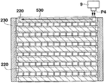
도 3 등에 나타내는 바와 같이, 격벽(200)의 개구부(201)는 발광층(300)의 형상을 규정한다. 개구부(201)는 열방향에, 스트라이프 형상으로 배열되어 있다.As shown in FIG. 3 and the like, the
개구부(201)는 평면형상이 예를 들면, 긴쪽방향(열방향)에 있어서의 양단이 폐구된, 대략 장방형의 형상으로 되어 있다. 이에 따라, 개구부(201)에 형성되는 발광층(300)은 열방향에 일렬로 늘어서는 복수의 화소에 걸쳐 형성되고, 개구부 (201)의 평면형상에 대응한 대략 장방형의 형상으로 형성되어 있다. 여기서, 개구부(201)의 평면형상은 양단이 폐구된 형상에 한하는 것이 아니라, 일단(一端)이 폐구되고, 타단(他端)이 개구된 것이라도 좋다.The
또한, 도 3 등에 기재된 격벽(200)은 Ⅶ-Ⅶ 단면도가 도 7a에 나타낸 바와 같은 구성의 경우, 격벽(200)의 높이가 층간 절연막(250)보다도 높기 때문에, 도 3 등에 있어서는 이해를 용이하게 하기 위해서, 개구부(251) 등을 적절히 생략해서 나타내고 있다. 또, 도 3 등에 기재된 격벽은 Ⅶ-Ⅶ 단면도가 도 7b에 나타낸 바와 같은 구성이라도 좋다.In addition, since the height of the
도 4와 같이, 격벽(200)은 열방향으로 연장하며, 서로 병행으로 배치설치된 복수의 제 1 격벽(220)을 구비한다. 제 1 격벽(220)은 도 4에 있어서, 진한 회색으로 나타낸 부분이다. 그리고, 복수의 제 1 격벽(220)은 스트라이프 형상으로 형성된 한 쌍의 제 1 격벽(A, B, C, …)을 복수조(複數組) 구성한다. 행방향에 있어서의 이웃이 되는 두개의 제 1 격벽(220)이 한 쌍의 제 1 격벽(A, B, C, …)을 구성한다. 여기서, 행방향이란, 열방향에 대해서 수직한 방향으로서, 도 4에 있어서의 도면 상하방향이다.As shown in FIG. 4, the
하나의 제 1 격벽(220)에 대해, 행방향에 있어서의 양측에 하나씩, 두개의 제 1 격벽(220)이 있을 경우에는, 중앙의 제 1 격벽(220)은 그 양측에 있는, 두개의 제 1 격벽(220) 각각과, 2조의 한 쌍의 제 1 격벽(A, B)을 구성한다.For one
즉, 하나의 제 1 격벽(220)(예를 들면, 도 4에 있어서의 위에서부터 2개째의 제 1 격벽(220))은 2조의 제 1 격벽(예를 들면, A 및 B)에 겸용될 경우가 있다.That is, one first partition 220 (for example, the second
격벽(200)은 한 쌍의 제 1 격벽(220)을 적어도 1조 구비한 형상이라면 좋다.The
제 1 격벽(220)은 제 1 방향(열방향)으로 장척(長尺)인 형상이며, 대략 장방형(장방형도 포함한다)의 형상을 갖는다.The
또한, 도 4와 같이, 격벽(200)은 제 1 격벽(A, B, C, …)의 긴쪽방향에 있어서, 한 쌍의 제 1 격벽(A, B, C, …)의 각각의 일단끼리를 연결하는 제 2 격벽 (230)을 구비한다. 제 2 격벽(230)은 도 4에 있어서, 빗금을 실시한 영역이다(이 빗금은 단면을 나타내는 것이 아니다). 여기서, 제 2 격벽(230)은 제 1 격벽(220)의 양단에 형성된다.In addition, as shown in FIG. 4, the
즉, 격벽(200)은 제 1 격벽(A, B, C, …)의 각각의 긴쪽방향에 있어서의, 한 쌍의 제 1 격벽(A, B, C, …)의 일단끼리를 연결하는, 두개의 제 2 격벽(230)을 각 제 1 격벽(220)의 양단에 구비한다.That is, the
또한, 격벽(200)은 제 2 격벽(230)을, 제 1 격벽(A, B, C, …)의 일단에만 하나 구비하는 것이라도 좋다. 즉, 제 2 격벽(230)은 적어도 하나 있으면 좋다. 제 2 격벽(230)이 하나인 경우, 개구부(201)는 평면형상이, 긴쪽방향에 있어서의 일단이 폐구되고, 타단이 개구된 형상(여기서는 대략 장방형)이 된다.In addition, the
제 1 격벽(220)과, 제 2 격벽(230)은 일체적으로 형성된다. 그리고, 제 1 격벽(220)과, 제 2 격벽(230)에 의해서 개구부(201)가 형성된다.The
개구부(201)와, 개구부(201)에 의해 노출된, 기판(100)의 영역에 의해서 홈이 형성된다. 즉, 제 1 격벽(220)과, 제 2 격벽(230)과, 기판(100)에 의해서 홈이 형성된다.The groove is formed by the
또한, 격벽(200)의 형상은 다른 형상이라도 좋다. 격벽(200)은 개구부(201)가 격자 형상이 되는 형상이라도 좋다. 이 경우, 긴쪽방향에 연장하는 격벽을 제 1 격벽(220)이라고 생각하고, 긴쪽방향에 수직으로 연장하는 격벽을 제 2 격벽 (230)이라고 생각하면 좋다.In addition, the shape of the
(3) 스텝S103(3) step S103
스텝S103에서는 격벽(200)의 표면(적당히 개구부(201)의 내벽면도 포함한다.)에 표면처리를 실행한다.In step S103, the surface treatment is performed on the surface of the partition 200 (it also includes the inner wall surface of the opening 201).
본원 발명자는 종래, 상기의 표면처리로서, 개구부(201)로부터 노출되는 기판(100)의 영역과, 격벽(200)의 표면 전면에 대해 친액화 처리를 실행하고 나서, 격벽(200)의 표면 전면에 발액화 처리를 실행하고 있었다.The inventors of the present invention have conventionally performed a lyophilic treatment on the region of the
상기 발액화 처리에 의해서, 격벽(200)의 개구부(201)(홈)에 도포된 잉크가, 격벽(200)의 표면으로부터 튀게 된다. 이에 따라, 잉크가 격벽(200)(특히 제 1 격벽(220))을 타고 넘어, 옆의 홈으로 진입해 버리는 것을 막도록 하고 있었다.By the liquid repelling treatment, the ink applied to the openings 201 (grooves) of the
그러나, 이와 같은 표면처리를 실행하고, 홈에 잉크를 도포해서 발광층(300)을 형성했을 경우에, 홈의 저면(개구부(201)에 의해서 규정되는 기판(100)의 표면)에 있어서 발광층(300)에 의해 덮여지지 않는 영역이 형성되어 버린다고 하는 현상이 생기는 일이 있는 것을, 본원 발명자는 발견했다.However, when the surface treatment is performed and ink is applied to the grooves to form the
그리고, 이 현상에 의해서, 제 1 격벽(220)의 장척방향에 있어서의 단부(端部) 근처에 있는 1 내지 복수의 화소전극(129) 등이 발광층(300)에 의해, 덮여지지 않게 되어 버리는 일이 있었다.By this phenomenon, one to the plurality of
또한, 친액화 처리로서는 자외선광의 조사에 의한 처리 또는 O2(산소) 플라즈마 처리 등이 있다. 또, 발액화 처리는 CF4(4 불화 메탄) 플라즈마 처리 등이 있다.In addition, the lyophilic treatment includes treatment by irradiation of ultraviolet light or O 2 (oxygen) plasma treatment. In addition, the liquid-repellent treatment includes a CF 4 (tetrafluoromethane) plasma treatment.
이와 같은 처리는 예를 들면, 일본국 특허 제3328297호 공보에 기재되어 있는 바와 같은 공지의 기술을 이용할 수 있다.Such a process can use the well-known technique as described, for example in Unexamined-Japanese-Patent No. 3328297.
또한, 발액성이란, 수계(水系)의 용매 또는 유기계 용매의 어느 하나를 소정 기준 이상의 정도로 튀기는 성질을 나타낸다. 또, 친액이란, 수계의 용매 또는 유기계 용매의 어느 하나를 소정 기준 미만의 정도로 튀기는 성질(즉, 소정 기준 이상의 정도로 튀기지 않는 성질)을 나타낸다. 여기서 소정 기준으로서, 예를 들면 접촉각의 각도의 값을 이용할 수 있으며, 예를 들면, 접촉각이 40도 이하일 때를, 친액성을 갖고 있다고 말하고, 접촉각이 50도 이상일 때를, 발액성을 갖고 있다고 말한다.In addition, liquid repellency shows the property which any one of an aqueous solvent or an organic solvent is fried to the grade more than a predetermined | prescribed criterion. In addition, a lyophilic liquid shows the property (that is, the property which does not fry to the grade more than a predetermined | prescribed criterion) to any one of an aqueous solvent or an organic solvent to below a predetermined | prescribed criterion. Here, as a predetermined criterion, for example, the value of the angle of the contact angle can be used. For example, when the contact angle is 40 degrees or less, it is said to have lipophilic property, and when the contact angle is 50 degrees or more, it has liquid repellency. Say.
도 8은 도 6에 있어서의 Ⅷ-Ⅷ 개략 단면도이다.FIG. 8 is a schematic sectional view taken along line VIII of FIG. 6.
도 9는 상기의 본원 발명자가 종래 실행하고 있었던 발광장치의 제조방법으로 발광층을 형성했을 때의, 발광층의 형상의 일례를 나타내는 도면이다.Fig. 9 is a diagram showing an example of the shape of the light emitting layer when the light emitting layer is formed by the method of manufacturing a light emitting device that the inventor of the present invention has conventionally performed.
본원 발명자는 다양한 검토의 결과, 홈의 저면에 있어서 발광층(300)에 의해서 덮여지지 않는 영역이 형성되어 버리는 상기 현상의 원인은 이하와 같은 점에 있는 것을 발견했다.As a result of various studies, the inventors of the present invention have found that the cause of the phenomenon in which the region not covered by the
상기 종래의 발액화 처리에서는 격벽(200) 전체를 발액화 처리하고 있었기 때문에, 제 2 격벽(230)의 표면도 발액화되어 있었다. 이 발액화 후에 잉크를 홈에 도포했을 경우, 특히, 홈의 저면 전면을 덮도록 잉크를 도포하므로, 잉크의 액면(液面)이 도 8의 액면(301)과 같은 형상이 되도록(노즐 프린팅의 경우 등에서는, 액면의 단부는 더욱 외측으로 이동하는 경우가 있다.), 잉크가 홈내를 채우도록 도포된다.In the above-mentioned conventional liquid-repellent treatment, the
이때에, 제 2 격벽(230)이 발액화되고 있으므로, 제 2 격벽(230) 위에 도포된 잉크가 격벽(230)의 표면에 의해서 튀어 버린다. 튀어진 잉크는 개구부(201)의 장척방향에 있어서의 개구부(201)의 내측으로 되밀린다.At this time, since the
이에 따라, 도 8의 액면(302)과 같이, 일단, 홈내를 채우도록 도포된 잉크의 액면(302)의 개구부(201)의 장척방향의 단부는, 격벽(230)의 표면에 의해 튀어져서, 개구부(201)의 단부보다도 내측으로 이동해 버린다. 이 때문에, 실제로 형성되는, 개구부(201)의 장척방향에 있어서의, 발광층(399)의 단부는 개구부(201)의 단부보다도 내측이 되어버린다(도 9 참조).Accordingly, as in the
이와 같은 원인에 의해서, 홈의 저면 전면을 덮도록 홈에 잉크를 도포해서 발광층(399)을 형성해도, 홈의 저면에 있어서 발광층(399)에 의해서 덮여지지 않는 영역이 형성되어 버리는 현상이 생기는 것을 본원 발명자는 발견했다. 종래는 이와 같은 현상에 의해 발광층(399)에 의해서 덮여지지 않는 영역이 생겨버리는 것을 예측해서, 그 영역을 미리 더미(dummy) 화소영역으로서 두는 일이 행해지고 있었다. 이 경우, 필요한 표시영역을 얻기 위한 기판(100)의 치수를, 더미 화소영역을 설치하는 만큼 크게 해야 했다.For this reason, even if the
또한, 도 8에서는 기판(100)이 구비하는 소자, 층간 절연막(250) 등을 적절히 생략하고 있다. 특히 도 8에서는 격벽(200)이 과장되어 표현되고, 소자 및 층간 절연막(250) 등은 생략되어 있다. 또, 도 9에서는 화소전극(129) 등을 적절히 생략하고 있다.In addition, in FIG. 8, the element,
그리고, 본원 발명자는 다양한 검토의 결과, 예를 들면, 스텝S103에서의 처리에 있어서, 제 2 격벽(230)의 발액도(撥液度)를, 제 1 격벽(220)의 긴쪽방향에 있어서의, 제 1 격벽(220)의 중앙의 발액도보다도 낮게 하는 처리를 실행하는 것에 의해, 상기의 좋지 못한 점을 해소 또는 개선할 수 있는 것을 발견했다.And the inventor of the present application, as a result of various examinations, for example, in the processing in step S103, the liquid repellency degree of the
즉, 제 2 격벽(230)의 발액도가 상대적으로 낮으면, 홈에 도포된 잉크가, 제 2 격벽(230)에 의해서 튀어지는 것을 방지 또는 경감할 수 있다. 이 때문에, 잉크가 상기와 같이, 상기의 장척방향에 있어서의 개구부(201)의 내측으로 되밀리는 것 (잉크의 되밀어냄)을 방지 또는 경감할 수 있다. 이에 따라, 격벽(200)과, 기판 (100)에 의해 형성되는 홈의 저면에 있어서 발광층(300)에 의해서 덮여지지 않는 영역이 생기지 않도록 하거나, 또는 덮여지지 않는 영역을, 종래보다 적게 할 수 있다. 여기서, 상기 종래의 발광장치의 제조방법에 있어서는, 발광층(399)의 단부가 어느 정도 개구부(201)의 단부보다도 내측이 되어 버리는지는 안정되어 있지 않았기 때문에, 상기의 더미 화소영역을 비교적 크게 해 두지 않으면 안되었다. 그러나, 본 실시형태에 있어서는, 발광층(399)의 단부가 개구부(201)의 단부에서 내측이 된다고 해도, 그 양은 근소하며 비교적 안정되어 있다. 그 때문에, 상기의 더미 화소영역을 설치한다고 해도, 그 더미 화소영역을 종래보다 작게 할 수 있다. 그리고 이에 따라, 필요한 표시영역을 얻기 위한 기판(100)의 치수를, 종래보다 작게 할 수 있다.That is, when the liquid repellency of the
여기서, 발액도는 예를 들면, 소정영역에 있어서의, 잉크와의 접촉각 또는 단위 면적당의 발액물질의 양에 의해서 결정된다. 즉, 단위 면적당의 발액물질의 양이 많을수록, 발액도가 높아진다.Here, the liquid repellency degree is determined by, for example, the contact angle with the ink or the amount of the liquid repellent substance per unit area in the predetermined region. That is, the greater the amount of the liquid-repellent substance per unit area, the higher the liquid-repellent degree.
제 1 격벽(220)의 중앙의 발액도는 제 1 격벽(220)의 중앙 표면의 영역(예를 들면, 도 4의 점선원(225)으로 둘러싸인 영역)의 발액도이면 좋다. 중앙이란, 중심 이외에, 그 근처도 포함하는 일이 있다.The liquid repellent degree in the center of the
제 2 격벽(230)의 발액도는 예를 들면, 제 2 격벽(230)중의 개구부(201)의 내벽면을 구성하는 면을 적어도 포함하는 영역(예를 들면, 도 4의 점선원(235)으로 둘러싸인 영역) 또는 그 면의 외측에 위치하는 격벽(230)의 표면의 영역을 적어도 포함하는 영역(예를 들면, 도 4의 점선원(236)으로 둘러싸인 영역)에서의 발액도인 것이 바람직하다.The liquid repellent degree of the
이들의 영역이, 상기의 잉크의 되밀어냄에 크게 기여하는 영역이라고 생각 되어지기 때문이다.It is because these areas are considered to be the area which greatly contributes to the repelling of said ink.
특히, 발액도는 예를 들면, 상기의 영역에 있어서의 단위 면적당의 발액물질의 양을 계측 함으로써, 파악할 수 있다.In particular, the liquid repellency degree can be grasped | ascertained by measuring the quantity of the liquid repellent substance per unit area in the said area, for example.
예를 들면, 점선원(225)의 영역의 단위 면적당의 발액물질의 양과, 점선원 (235)의 영역 또는 상기의 점선원(236)의 영역의 단위 면적당의 발액물질의 양을 비교했을 경우에, 점선원(225)의 영역 쪽의 단위 면적당의 발액물질의 양을 많이 함으로써, 제 2 격벽(230)의 발액도를, 상기의 긴쪽방향에 있어서의 제 1 격벽 (220)의 중앙의 발액도보다도 낮게 한다.For example, when the amount of the liquid repellent substance per unit area of the area of the dotted
발액물질이란, 예를 들면, 불소 또는 불소계 화합물 등의 발액처리에 사용되는 물질(발액성을 가지는 물질)이다.A liquid repellent substance is a substance (material having liquid repellency) used for liquid repellent treatment, such as fluorine or a fluorine-type compound, for example.
이와 같이, 제 1 격벽(220)의 중앙의 표면이, 제 2 격벽(230)의 표면보다도 발액물질을 많이 포함하도록 처리하는 것에 의해, 상기와 같이, 격벽(200)과, 기판 (100)에 의해 형성되는 홈의 저면에 있어서 발광층(300)에 의해서 덮여지지 않는 영역을 없애거나 적게 할 수 있다.As described above, by treating the surface of the center of the
여기서, 스텝S103에 있어서의 표면처리에 적용할 수 있는, 두개의 실시예에 대해 설명한다.Here, two embodiments that can be applied to the surface treatment in step S103 will be described.
또한, 하기에서 설명하는 친액화 및 발액화하는 방법에 대해서는 상기의 공지의 방법을 적절히 채용할 수 있다. 또, 다음의 O2(산소) 플라즈마 처리는 적절 자외선광의 조사에 의한 처리 등으로 적절히 변경할 수 있다. 또, 다음의 CF4 플라즈마 처리도 다른 처리로 적절히 변경할 수 있다.In addition, the well-known method mentioned above can be employ | adopted suitably for the method of lyophilizing and liquid repellency demonstrated below. In addition, the following O 2 (oxygen) plasma treatment can be appropriately changed by treatment with appropriate ultraviolet light irradiation or the like. In addition, the following CF 4 plasma treatment can also be appropriately changed to another treatment.
a. 제 1 실시예a. First embodiment
우선, 스텝S103에 있어서의 표면처리에 적용할 수 있는 제 1 실시예에 대해 설명한다.First, the first embodiment that can be applied to the surface treatment in step S103 will be described.
도 10은 도 2의 스텝S103의 표면처리에 적용할 수 있는, 제 1 실시예를 설명하기 위한 흐름도이다.FIG. 10 is a flowchart for explaining the first embodiment which can be applied to the surface treatment of step S103 in FIG.
도 11a, 도 11b∼도 13은 제 1 실시예의 친액화 처리의 일례를 설명하기 위한 도면이다.11A and 11B to 13 are diagrams for explaining an example of the lyophilic treatment of the first embodiment.
상기 제 1 실시예에서는 우선, 개구부(201)로부터 노출하는 기판(100)의 영역과, 격벽(200)의 표면 전면에 대해서 친액화 처리한다(스텝S103a).In the first embodiment, first, the area of the
구체적으로는, O2 플라즈마를, 개구부(201)로부터 노출하는 기판(100)의 영역과, 격벽(200)의 표면 전면을 포함하는 영역(도 11a의 이점쇄선 참조)에 조사하는 것에 의해, 이들의 영역을 친액화한다.Specifically, by irradiating the O 2 plasma to the region of the
상기 친액화 처리는 예를 들면, 주지의 평행 평판형 또는 배럴식의 플라즈마 조사장치를 이용해서 실행할 수 있다. 이 경우, 스텝S102에서 격벽(200)이 형성된 기판(100)을, 이 플라즈마 조사장치내에 설치하고, 개구부(201)로부터 노출하는 기판(100)의 영역 및 격벽(200)의 표면 전면에 한번에 O2 플라즈마를 조사하는 것으로, 일괄해서 한번에 친액화 처리할 수 있다.The said lyophilic process can be performed using a well-known parallel flat plate type or barrel type plasma irradiation apparatus, for example. In this case, in step S102, the
또, 상기 친액화 처리를 스폿형의 플라즈마 조사장치(9)를 이용해서 실행할 수도 있다. 이 경우의 구성을 도 11a에 나타낸다.The lyophilic treatment can also be performed using the spot type
여기서, 스폿형의 플라즈마 조사장치(9)의 개요를, 도 11b에 나타낸다. 스폿형의 플라즈마 조사장치(9)는 도 11b에 나타내는 바와 같이, 내부에 플라즈마 발생용의 전극(9b)을 구비하고, 전극(9b)에 고주파 전압(9c)이 인가된다. 그리고, 전극(9b) 사이에 CF4 또는 O2와 아르곤 등을 포함하는 가스가 공급되고, 공급된 가스에 따른 플라즈마를 생성하는 반응기(9a)를 가지며, 반응기(9a)의 선단 부분에 설치된 개구부(9d)로부터, 반응기(9a)내에서 생성된 플라즈마를 스폿적(국소적)으로 플라즈마 제트(P1)로서 방출하는 장치이다.Here, the outline | summary of the spot type
이 경우, 도 11a에 나타내는 바와 같이, 플라즈마 조사장치(9)를 화살표 (500)와 같이 움직여서, 개구부(201)로부터 노출하는 기판(100)의 영역과, 격벽 (200)의 표면 전면을 포함하는 영역에 O2 플라즈마 제트(P1)를 조사한다.In this case, as shown in FIG. 11A, the
이 처리에 의해서, 개구부(201)로부터 노출하는 기판(100)의 영역과, 격벽 (200)의 표면 전면에 잔류되는 잔류물 등을 제거하고, 이들의 영역을 친액화할 수 있다.By this process, the area | region of the board |
다음에, 격벽(200)의 전면을 발액화 처리한다(스텝S103b).Next, the entire surface of the
구체적으로는 도 12와 같이, 스폿형의 플라즈마 조사장치(9)에 의해서, CF4 플라즈마 제트(P2)를 격벽(200)의 전면에 조사한다(이점쇄선 참조).Specifically, as shown in FIG. 12, the CF 4 plasma jet P2 is irradiated onto the entire surface of the
또한, 도 12에서는, 플라즈마 조사장치(9)는 화살표(510)와 같이 움직여서, CF4 플라즈마 제트(P2)를 격벽(200)의 전면에 조사한다. 플라즈마 조사장치(9)는 개구부(201)를 통해 노출하는 기판(100)의 표면에 조사되지 않도록 움직여서, CF4 플라즈마 제트(P2)를 격벽(200)의 전면에 조사하면 좋다. 이와 같은 CF4 플라즈마 처리에 의해서, 격벽(200)의 표면에 불소가 잔류되고, 격벽(200)의 표면이 발액화된다.In Figure 12, the
다음에, 제 2 격벽(230)을 친액화 처리한다(스텝S103c).Next, the
구체적으로는 도 13과 같이, 스폿형의 플라즈마 조사장치(9)에 의해서, O2 플라즈마 제트(P3)를 제 2 격벽(230)에 조사한다(이점쇄선 참조).Specifically, as shown in FIG. 13, the O 2 plasma jet P3 is irradiated to the
또한, 도 13에서는, 플라즈마 조사장치(9)는 화살표(520)와 같이 움직여서, O2 플라즈마 제트(P3)를 제 2 격벽(230)에 조사한다. O2 플라즈마 제트(P3)가 조사된 영역은 O2에 의해서 불소가 제거되며 친액화된다.In Figure 13, the
이상과 같이 하여, 제 2 격벽(230)의 발액도를, 상기의 긴쪽방향에 있어서의 제 1 격벽(220)의 중앙의 발액도보다도 낮게 하는 처리가 실행된다.As mentioned above, the process which makes the liquid repellency degree of the
또한, 도 11 내지 도 13에 있어서의 그물 부분 및 빗금은 제 1 격벽(220)과, 제 2 격벽(230)을 명료하게 하기 위한 것이다(도 15에 있어서도 마찬가지임). 특히, 도 11 내지 도 13에 있어서의 빗금은 단면을 나타내는 것이 아니다(도 15에 있어서도 마찬가지임).In addition, the net part and the hatched in FIGS. 11-13 are for clarifying the
또한, 격벽(200)을 발액화한 후에, 제 2 격벽(230)을 친액화한다는 것은, 제 1 격벽(220)의 장척방향에 있어서의 제 1 격벽(220)의 단부에 대해서도, 친액화 처리하는 것도 포함한다(도 13참조).In addition, the liquefaction of the
이에 따라, 제 1 격벽(220)의 단부의 발액도는 제 1 격벽의 중앙의 발액도보다도 낮아진다. 이로써, 잉크의 되밀어냄을 더욱, 방지 또는 경감할 수 있다.As a result, the liquid repellency degree at the end of the
또한, 제 2 격벽(230)을 친액화할 때에는 적어도, 제 2 격벽(230)의 개구부 (201)측의 표면(특히, 개구부(201)를 구성하는 내벽면)을 친액화하는 것이 바람직하다. 이에 따라, 잉크의 밀어 되밀어냄을 정밀도 좋게, 방지 또는 경감할 수 있다.In addition, when lyophilizing the
상기와 같이, 제 1 격벽(220)과 제 2 격벽(230)을 발액화한 후에, 적어도 제 2 격벽(230)을 친액화하는 것으로, 종래의 통상의 발액화 처리의 뒤에, 제 2 격벽 (230)을 친액화할 수 있다.As described above, after the
또한, 제 2 격벽(230)은 영역이 비교적 좁으므로, 플라즈마 조사장치(9)의 이동거리는 작다. 이 때문에, 종래, 실행하고 있었던 처리에 조금의 변경을 부가하는 것 만으로, 용이하게 제 2 격벽(230)의 발액도를, 상기의 긴쪽방향에 있어서의 제 1 격벽(220)의 중앙의 발액도보다도 낮게 하는 처리를 할 수 있다.In addition, since the area of the
b. 제 2 실시예b. Second embodiment
다음에, 스텝S103에 있어서의 표면처리에 적용할 수 있는 제 2 실시예에 대해 설명한다.Next, a second embodiment that can be applied to the surface treatment in step S103 will be described.
도 14는 도 2의 스텝S103의 표면처리에 적용할 수 있는, 제 2 실시예를 설명하기 위한 흐름도이다.FIG. 14 is a flowchart for explaining a second embodiment which can be applied to the surface treatment of step S103 in FIG.
도 15는 제 2 실시예의 발액화 처리의 일례를 설명하기 위한 도면이다.FIG. 15 is a view for explaining an example of the liquid-repellent treatment of the second embodiment.
상기 제 2 실시예에서는 우선, 개구부(201)로부터 노출하는 기판(100)의 영역과, 격벽(200)의 표면 전면에 대해서 친액화 처리를 실행한다(스텝S103d).In the second embodiment, first, a lyophilic treatment is performed on the region of the
상기 처리는 상기의 제 1 예에 있어서의 스텝S103a의 처리와 마찬가지 이므로, 설명을 생략한다.Since the processing is the same as the processing in step S103a in the first example, description thereof is omitted.
다음에, 제 1 격벽(220)에 발액화 처리한다(스텝S103e).Next, a liquid repelling process is performed on the first partition wall 220 (step S103e).
구체적으로는 도 15와 같이, 스폿형의 플라즈마 조사장치(9)에 의해서, CF4 플라즈마 제트(P4)를 제 1 격벽(220)에 조사한다(이점쇄선 참조).Specifically, as shown in FIG. 15, the CF 4 plasma jet P4 is irradiated to the
또한, 도 15에서는, 플라즈마 조사장치(9)는 화살표와 같이 움직여서, CF4 플라즈마 제트(P4)를 제 1 격벽(220)에 조사한다. 이때, 플라즈마 조사장치(9)는 개구부(201)를 통해 노출하는 기판(100)의 표면에 조사되지 않도록 움직여서, CF4 플라즈마 제트(P4)를 격벽(200)의 전면에 조사하면 좋다. 또, 제 1 격벽(220)의 긴쪽방향에 있어서의 제 1 격벽(220)의 단(端) 까지, CF4 플라즈마 제트(P4)를 조사할 필요는 없다.In Figure 15, the
제 1 격벽(220)의 장척방향에 있어서의 제 1 격벽(220)의 단부를 친액화해 둠으로써, 제 1 격벽(220)의 단부의 발액도는 제 1 격벽의 중앙의 발액도보다도 낮아진다. 이에 따라, 잉크의 되밀어냄을 더욱, 방지 또는 경감할 수 있다.By making the end part of the
상기 CF4 플라즈마 처리에 의해서, 제 1 격벽(220)의 표면에 불소가 잔류되고, 제 1 격벽(220)의 표면이 발액화된다. 이와 같이 해서, 제 2 격벽(230)의 발액도를, 상기의 긴쪽방향에 있어서의 제 1 격벽(220)의 중앙의 발액도보다도 낮게 하는 처리가 실행된다.By the CF 4 plasma treatment, fluorine remains on the surface of the
상기와 같이, 제 1 격벽(220)의 적어도 일부(특히 긴쪽방향에 있어서의 제 1 격벽(220)의 중앙을 포함하는 대부분(예를 들면, 90퍼센트 이상)을 발액화하고, 제 2 격벽(230)을 발액화하지 않는 것으로, 제 1 예에 비해 플라즈마 처리의 회수를 적게 할 수 있다.As described above, at least part of the first partition wall 220 (particularly 90% or more) including the center of the
또한, 제 2 격벽(230)의 발액도가 제 1 격벽(220)의 긴쪽방향에 있어서의 제 1 격벽(220)의 중앙의 발액도보다도 낮아지면, 제 1 예 및 제 2 예에 있어서, 스텝S103a 또는 스텝S103d를 생략해도 좋다. 이 경우에도, 상기와 마찬가지의 효과를 얻을 수 있을 경우가 있다.In addition, when the liquid repellency degree of the
구체적으로는, 제 1 잉크를 개구부(201)내(홈)에 도포한다. 그리고, 도포한 제 1 잉크중의 용매를 건조시키는 것에 의해, 발광층(300)을 형성한다. 또, 발광장치(1)가 R(Red), G(Green) 및 B(Blue)의 화소를 가질 경우에는 잉크(특히 후술의 중심층을 형성하는 잉크)의 도포를 나눈다.Specifically, the first ink is applied into the opening 201 (groove). And the
제 1 잉크는 발광하는 것이 가능한 공지의 고분자 발광재료, 예를 들면 폴리파라페닐렌비닐렌계(polyparaphenylenevinyl) 또는 폴리플루오렌(polyfluorene)계 등의 공역이중결합 폴리머를 포함하는 발광재료를 포함한다. 이 고분자 발광재료가 용매에 용해 또는 분산된 액체가 잉크가 된다. 용매는 예를 들면, 수계 용매, 또는 테트랄린(tetralin), 테트라메틸렌벤젠(tetramethylenebenzen), 메시틸렌 (mesitylene), 또는 크실렌 등의 유기 용매이다. 이와 같은 제 1 잉크를 이용해서 형성된 층은 발광이 실행되는 층이며, 발광층(300)의 중심적인 층이 된다. 이 층을 이하에서는 중심층이라고 한다.The first ink includes a known polymer light emitting material capable of emitting light, for example, a light emitting material containing a conjugated double bond polymer such as polyparaphenylenevinyl or polyfluorene. The liquid in which the polymer light emitting material is dissolved or dispersed in a solvent becomes an ink. The solvent is, for example, an aqueous solvent or an organic solvent such as tetralin, tetramethylenebenzene, mesitylene, or xylene. The layer formed using such a first ink is a layer for emitting light and becomes a central layer of the
제 1 잉크를 도포하는 방법은 토출 노즐을 이용해서 잉크를 계속해서 배출하는 노즐 프린팅 또는 잉크젯에 의한 잉크젯 프린팅 등으로 실현된다. 상술한 바와 같이, 제 1 잉크는 홈의 저면 전면을 덮도록 도포된다(도 8의 액면(301) 참조). 이때, 제 2 격벽(230)이 발액화되어 있지 않으(특히, 친액화되어 있다)므로, 잉크의 되밀어냄을 방지 또는 경감할 수 있다. 이 때문에, 격벽(200)과, 기판(100)에 의해서 형성되는 홈의 저면에 있어서 발광층(300)에 의해 덮여지지 않는 영역을 없애거나 적게 할 수 있다. 도 5 등에서는 홈의 저면에 있어서 발광층(300)에 의해서 덮여지지 않는 영역이 없어져 있다.The method of applying the first ink is realized by nozzle printing for continuously discharging ink using an ejection nozzle, inkjet printing by inkjet, or the like. As described above, the first ink is applied to cover the entire bottom surface of the groove (see
또, 도포한 제 1 잉크 중의 용매를 건조시키는 방법은 대기 분위기중에서의 건조, 질소 분위기중에서의 건조, 진공중에서의 건조, 또는 이들 중 어느 하나의 분위기중에서의 가열건조 등, 공지의 방법을 채용할 수 있다.As a method of drying the solvent in the applied first ink, a known method such as drying in an air atmosphere, drying in a nitrogen atmosphere, drying in a vacuum, or heating drying in any one of these atmospheres may be employed. Can be.
발광층(300)은 화소전극(129)(애노드 전극) 및 대향전극(캐소드 전극)(400)에 의해 인가되는 전압에 의해서 발광하는 층이다.The
발광층(300)은 상기에서는, 중심층으로부터 형성되지만, 발광층(300)은 도 16에 나타내는 바와 같이, 중심층(310)과, 정공 주입층(330)과, 인터 레이어(350)를 구비한 것이라도 좋다. 발광층(300)은 적어도 중심층(310)을 구비하는 것이면 좋다.Although the
발광층(300)이 정공 주입층(330)을 구비할 경우, 상기의 중심층(310)을 형성하기 전에, 제 2 잉크를 개구부(201)내(홈)에 도포하고, 도포한 제 2 잉크중의 용매를 건조시키는 것에 의해, 정공 주입층(330)을 형성한다.When the
상기 정공 주입층(330)은 화소전극(129)과 중심층(310)(인터 레이어(350))의 사이에 형성된다. 정공 주입층(330)은 중심층(310)에 정공을 공급하는 기능을 갖는다. 정공 주입층(330)은 정공(홀)주입ㆍ수송이 가능한 유기 고분자계의 재료, 예를 들면 도전성 폴리머인 폴리에틸렌디옥시티오펜(PEDOT)과 도펀트인 폴리스틸렌 설포네이트(PSS)로 구성된다. 즉, 제 2 잉크는 상기의 유기 고분자계의 재료가, 수계 용매 또은 테트랄린, 테트라메틸렌벤젠, 메시틸렌, 또는 크실렌 등의 유기 용매의 용매에, 용해 또는 분산된 액체이다. 제 2 잉크를 도포하는 방법은 예를 들면, 토출 노즐을 이용해서 잉크를 계속해서 배출하는 노즐 프린팅 또는 잉크젯에 의한 잉크젯 프린팅 등으로 실현된다. 제 2 잉크는 홈의 저면 전면을 덮도록 도포된다(도 8의 액면(301)과 마찬가지임). 이때, 제 2 격벽(230)이 발액화되어 있지 않으(특히, 친액화되어 있다)므로, 잉크의 되밀어냄을 방지 또는 경감할 수 있다. 이 때문에, 격벽(200)과, 기판(100)에 의해서 형성되는 홈의 저면에 있어서 발광층(300)(특히, 정공 주입층(330))에 의해 덮여지지 않는 영역을 없애거나 적게 할 수 있다.The
또한, 정공 주입층(330)을 형성 후에, 상기 스텝S103과 마찬가지의 처리를 실행해도 좋다. 이에 따라, 중심층(310) 또는 후술의 인터 레이어(350)를 형성할 때의 제 1 잉크 또는 제 2 잉크의 되밀어냄을 더욱 방지 또는 경감할 수 있다.After the
발광층(300)이 인터 레이어(350)를 구비할 경우, 상기의 중심층(310)을 형성하기 전에, 제 3 잉크를 개구부(201)내(홈)에 도포하고, 도포한 제 3 잉크중의 용매를 건조시키는 것에 의해, 인터 레이어(350)를 형성한다. 이 인터 레이어(350)는 정공 주입층(330)과 중심층(310)의 사이에 형성된다. 인터 레이어(350)는 정공 주입층(330)으로부터의 전자를 막고, 발광층(300)내에 있어서 전자와 정공을 재결합시키기 쉬워지는 기능을 가지며, 발광층(300)의 발광효율을 높인다. 인터 레이어(350)는 발광층(300)으로부터의 전자를 막는, 적절한 유기 고분자계의 재료로 구성된다. 즉, 제 3 잉크는 상기의 유기 고분자계의 재료가, 수계 용매 또는 테트랄린, 테트라메틸렌벤젠, 메시틸렌, 또는 크실렌 등의 유기 용매의 용매에, 용해 또는 분산된 액체다.In the case where the
제 3 잉크를 도포하는 방법은 예를 들면, 토출 노즐을 이용해서 잉크를 계속해서 배출하는 노즐 프린팅 또는 잉크젯에 의한 잉크젯 프린팅 등으로 실현된다. 제 3 잉크는 홈의 저면 전면을 덮도록 도포된다(도 8의 액면(301)과 마찬가지임). 또한, 인터 레이어(350)를 형성 후에, 상기 스텝S103과 마찬가지의 처리를 실행해도 좋다. 이에 따라, 중심층(310)을 형성할 때의 제 1 잉크의 되밀어냄을 더욱 방지 또는 경감할 수 있다.The method of applying the third ink is realized by, for example, nozzle printing for continuously discharging ink using an ejection nozzle, inkjet printing by inkjet, or the like. The third ink is applied to cover the entire bottom surface of the groove (same as the
(5) 스텝S105(5) step S105
스텝S105에서는 대향전극(400)을 형성한다.In step S105, the
대향전극(400)은 발광층(300) 위에 형성된다. 대향전극(400)은 도전재료, 예를 들면 Li, Mg, Ca, Ba 등의 일함수가 낮은 재료로 이루어지는 전자 주입성의 하층과, Al 등의 광반사성 도전금속으로 이루어지는 상층을 갖는 적층구조이다. 대향전극(400)은 발광층(300)이 형성된 후의 기판의 대략 전면에 형성된 하나의 전극 적층체로 구성된다(도 6참조).The
대향전극(400)은 예를 들면, 접지 전위인 공통전압(Vss)이 인가되어 있다.The
대향전극(400)은 진공 증착이나 스퍼터링에 의해서 형성된다.The
각 발광소자는 각 화소전극(129)과, 각 화소전극과 겹치는 위치에 있는 발광층(300)의 각 영역과, 각 화소전극과 발광층(300)을 통해 겹치는 위치에 있는 대향전극(400)의 각 영역에 의해서 구성된다.Each light emitting element includes each
(6)스텝S106(6) step S106
스텝S106에서는 밀봉을 실행한다.In step S106, sealing is performed.
발광소자를 갖는 복수의 화소(PIX)가 복수 형성된 표시영역(150)의 외측에 있어서, 대향전극(400) 형성 후의 기판(100) 위에 자외선 경화수지 또는 열경화 수지로 이루어지는 밀봉수지를 도포하고, 도시하지 않은 밀봉기판과 기판(100)을 서로 붙인다.Outside the
다음에 자외선 또는 열에 의해서 밀봉수지를 경화시킨다. 이에 따라, 기판 (100)과 밀봉기판을 접합한다.Next, the sealing resin is cured by ultraviolet rays or heat. As a result, the
이상에 의해 발광장치(1)가 제조된다.The light emitting device 1 is manufactured by the above.
본 실시형태에 관한 발광장치(1)는 기판(100)의 제 2 격벽(230)의 발액도가, 제 1 격벽(220)의 긴쪽방향에 있어서의 제 1 격벽(220)의 중앙의 발액도보다도 낮게 설정되어 있다.In the light emitting device 1 according to the present embodiment, the liquid repellent degree of the
또, 본 실시형태에 관한 발광장치(1)는 상기와 같이, 제 1 격벽(220)의 중앙의 표면은 제 2 격벽(230)의 표면보다도 발액물질을 많이 포함하도록 구성되어 있다.As described above, the light emitting device 1 according to the present embodiment is configured such that the surface of the center of the
이에 따라, 상기 발광장치(1)에서는 상기에서 설명한대로, 격벽(200)(한 쌍의 제 1 격벽(A, B, C, …) 및 적어도 하나의 제 2 격벽(230))과, 기판(100)에 의해서 형성되는 홈의 저면에 있어서 발광층(300)에 의해 덮여지지 않는 영역이 생기지 않도록 하거나, 덮여지지 않는 영역을 종래보다 적게 할 수 있다.Accordingly, in the light emitting device 1, as described above, the partition 200 (a pair of first partitions A, B, C, ...) and at least one
본 실시형태에 관한 발광장치(1)를 이용한 전자기기에 대해 설명한다.An electronic device using the light emitting device 1 according to the present embodiment will be described.
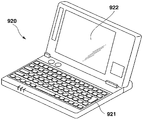
이와 같은 구성을 취하는 발광장치(1)는 예를 들면, 디지털 카메라, PC, 또는 휴대전화 등의 전자기기의 표시부(디스플레이)에 채용된다.The light emitting device 1 having such a configuration is employed in a display portion (display) of, for example, an electronic device such as a digital camera, a PC, or a cellular phone.
구체적으로는, 디지털 카메라(910)는 예를 들면 도 17 및 도 18과 같이, 조작부(911)와, 표시부(912)를 구비한다. 이 표시부(912)에 발광장치(1)가 채용된다.Specifically, the
마찬가지로, PC(920)는 도 19에 나타내는 바와 같이, 조작부(921)와, 표시부 (922)를 구비하고, 발광장치(1)는 표시부(922)에 사용된다.Similarly, as shown in FIG. 19, the
또한, 도 20에 나타내는 바와 같이, 휴대전화(930)는 조작부(931)와, 표시부 (932)를 구비하고, 발광장치(1)는 표시부(932)에 사용된다.20, the
상기 실시형태에 있어서는 발광장치(1)는 발광층(300)이 출사(出射)하는 광을 기재(110)측으로부터 외부에 출사하는 소위 버텀 에미션(bottom-emission)형의 발광장치라고 해서 설명했다. 그러나, 발광장치(1)는 예를 들면, 발광층(300)이 출사하는 광을 기재(110)의 반대측으로부터 외부에 출사하는 탑 에미션(top-emission)형의 발광장치라도 좋다.In the above embodiment, the light emitting device 1 has been described as a so-called bottom emission type light emitting device that emits light emitted from the
또, 상기 실시형태에 있어서의 잉크의 도포방법(인쇄방법)은 상기 노즐 프린팅 등에 한하지 않고, 예를 들면, 활판인쇄, 플랙시블 인쇄 등의 철판(凸版)인쇄법, 오프셋 인쇄 등의 평판인쇄, 그라비아 인쇄(gravure printing) 등의 요판(凹版)인쇄, 스크린 인쇄 등의 공판인쇄 등이라도 좋다.In addition, the ink application method (printing method) in the said embodiment is not limited to the said nozzle printing etc., For example, flat plate printing methods, such as iron plate printing methods, such as letterpress printing and flexible printing, offset printing, etc. Or gravure printing such as gravure printing, or gravure printing such as screen printing.
또, 본 실시형태에 있어서의 발광장치(1)는 상기와 같이 표시장치에 사용할 수 있지만, 또한, 발광장치(1)를 예를 들면, 프린터의 감광 드럼에 광을 조사하는 프린터 헤드 등의 노광장치에 이용해도 좋다.In addition, although the light emitting device 1 in this embodiment can be used for a display apparatus as mentioned above, exposure of the light emitting device 1, such as a printer head which irradiates light to the photosensitive drum of a printer, for example You may use it for an apparatus.
1: 발광장치 9: 플라즈마 조사장치
9a: 반응기 9b: 전극
9c: 고주파 전압 9d: 개구부
100: 기판 110: 기재
120: 적층체 121: 배선
122: 트랜지스터 122d: 드레인 전극
122g: 게이트 전극 122s: 소스 전극
123: 절연막 124: 스토퍼막
125: 반도체층 126, 127: 오믹 콘택트층
129: 화소전극(애노드 전극) 150: 표시영역
200: 격벽 201, 251: 개구부
220: 제 1 격벽 230: 제 2 격벽
250: 층간 절연막 300, 399: 발광층
301, 302: 액면 310: 중심층
330: 정공 주입층 350: 인터 레이어
400: 대향전극(캐소드 전극) 910: 디지털 카메라
911: 조작부 912: 표시부
920: PC 921: 조작부
922: 표시부 930: 휴대전화
931: 조작부 932: 표시부1: Light emitting device 9: Plasma irradiation device
9a:
9c:
100: substrate 110: substrate
120: laminate 121: wiring
122:
122g:
123: insulating film 124: stopper film
125:
129: pixel electrode (anode electrode) 150: display area
200:
220: first partition 230: second partition
250:
301, 302: liquid level 310: center layer
330: hole injection layer 350: inter layer
400: counter electrode (cathode electrode) 910: digital camera
911: operation unit 912: display unit
920: PC 921: control panel
922: Display unit 930: Mobile phone
931: operation unit 932: display unit
Claims (19)
기판과,
상기 기판 위에 형성된 격벽과,
상기 격벽에 의해 간막이된 적어도 하나의 홈내에 형성된, 상기 발광소자의 발광층을 구비하고,
상기 격벽은,
제 1 방향으로 연장해서 형성된 복수의 제 1 격벽과,
상기 제 1 방향과 직교하는 제 2 방향으로 연장하며, 상기 복수의 제 1 격벽의 단부끼리를 연결하도록 형성된 적어도 1개의 제 2 격벽을 갖고,
상기 제 2 격벽의 발액도는 각 상기 제 1 격벽의 상기 제 1 방향을 따른 양단 사이의 중앙의 영역의 발액도보다도 낮은 것을 특징으로 하는 발광장치.A light emitting device having at least one pixel having a light emitting element,
Substrate,
Barrier ribs formed on the substrate;
A light emitting layer of the light emitting element formed in at least one groove partitioned by the partition wall,
The partition wall,
A plurality of first partition walls extending in a first direction,
Has at least one second partition wall extending in a second direction orthogonal to the first direction and formed to connect end portions of the plurality of first partition walls,
The liquid repellent degree of the said 2nd partition wall is lower than the liquid repellency degree of the area | region in the center between the both ends along the said 1st direction of each said 1st partition wall.
상기 제 1 격벽 및 상기 제 2 격벽은 각각의 표면에, 그 단위 면적당의 양이 많을수록 상기 발액도가 높아지는 발액물질을 갖고,
상기 제 2 격벽의 표면에 갖는 상기 발액물질의 양은 상기 제 1 격벽의 상기 중앙의 영역의 표면에 갖는 상기 발액물질의 양보다 적은 것을 특징으로 하는 발광장치.The method of claim 1,
The first partition wall and the second partition wall have a liquid-repellent material on each surface of which the liquid repellency is higher as the amount per unit area increases.
The amount of the liquid-repellent material on the surface of the second partition wall is less than the amount of the liquid-repellent material on the surface of the central region of the first partition wall.
상기 발액물질은 불소 또는 불소계 화합물인 것을 특징으로 하는 발광장치.The method of claim 2,
The light emitting device, characterized in that the liquid-repellent material is a fluorine or fluorine-based compound.
1개의 상기 홈은 상기 기판 위에, 인접해서 형성된 한 쌍의 상기 제 1 격벽과, 상기 제 2 격벽에 의해 간막이되어 설치되어 있는 것을 특징으로 하는 발광장치.The method of claim 1,
The light emitting device according to claim 1, wherein one groove is provided on the substrate by a pair of adjacent first partitions and a second partition.
각 상기 화소는 상기 제 1 방향을 따라 배치설치되며,
상기 홈은 상기 복수의 화소의 상기 발광소자의 상기 발광층을 형성하는 영역에 걸쳐 설치되어 있는 것을 특징으로 하는 발광장치.The method of claim 1, further comprising a plurality of the pixels,
Each pixel is disposed along the first direction,
And the groove is provided over an area forming the light emitting layer of the light emitting element of the plurality of pixels.
상기 제 2 격벽을 2개 갖고, 각 해당 제 2 격벽의 한 쪽은 각 상기 제 1 격벽의 상기 제 1 방향에 있어서의 한 쪽의 단부끼리를 연결하며, 각 상기 제 2 격벽의 다른 쪽은 각 상기 제 1 격벽의 상기 제 1 방향에 있어서의 다른 쪽의 단부끼리를 연결하도록 형성되고,
상기 홈의 상기 제 1 방향에 있어서의 양단은 상기 제 2 격벽에 의해 닫혀져 있는 것을 특징으로 하는 발광장치.The method of claim 1,
It has two said 2nd partitions, One side of each said 2nd partition wall connects one edge part in the said 1st direction of each said 1st partition wall, The other side of each said 2nd partition wall is each It is formed so that the other edge part in the said 1st direction of the said 1st partition wall may connect,
Both ends of the groove in the first direction are closed by the second partition wall.
상기 격벽은 상기 절연막을 덮도록 형성되며,
상기 절연막은 상기 홈내에 노출되어 있지 않은 것을 특징으로 하는 발광장치.The semiconductor device according to claim 1, further comprising: a plurality of drive elements for driving the light emitting element formed on the substrate, and an insulating film covering the plurality of drive elements;
The partition wall is formed to cover the insulating film,
And the insulating film is not exposed in the groove.
상기 격벽은 절연재료에 의해 형성되어 있는 것을 특징으로 하는 발광장치.The method of claim 1,
And the partition wall is formed of an insulating material.
상기 표시부는 표시 데이터에 따른 화상정보를 표시하는 표시장치를 구비하며,
상기 표시장치는,
기판과,
상기 기판 위에 형성된 격벽과,
상기 격벽에 의해 간막이된 적어도 하나의 홈내에 형성된, 발광소자의 발광층을 구비하고,
상기 격벽은,
제 1 방향으로 연장해서 형성된 복수의 제 1 격벽과,
상기 제 1 방향과 직교하는 제 2 방향으로 연장하며, 각 상기 제 1 격벽의 단부끼리를 연결하도록 형성된 적어도 1개의 제 2 격벽을 갖고,
상기 제 2 격벽의 발액도는 각 상기 제 1 격벽의 상기 제 1 방향을 따른 양단 사이의 중앙의 영역의 발액도보다도 낮은 것을 특징으로 하는 전자기기.Has an operation unit and a display unit,
The display unit includes a display device for displaying image information according to display data,
The display device,
Substrate,
Barrier ribs formed on the substrate;
And a light emitting layer of the light emitting element, formed in at least one groove partitioned by the partition wall,
The partition wall,
A plurality of first partition walls extending in a first direction,
Has at least one second partition wall extending in a second direction orthogonal to the first direction and formed to connect end portions of the first partition walls,
The liquid repellency degree of the said 2nd partition wall is lower than the liquid repellency degree of the area | region between the both ends along the said 1st direction of each said 1st partition wall.
기판 위에 복수의 제 1 격벽을, 제 1 방향으로 연장하며, 상기 발광소자의 발광층의 형성영역을 간막이하도록 형성하고, 적어도 1개의 제 2 격벽을, 상기 제 1 방향과 직교하는 제 2 방향으로 연장하며, 상기 복수의 제 1 격벽의 단부끼리를 연결하도록 형성하는 격벽형성스텝과,
상기 제 2 격벽의 발액도가 각 상기 제 1 격벽의 상기 제 1 방향을 따른 양단 사이의 중앙의 영역의 발액도보다 낮아지도록, 각 상기 제 1 격벽과 상기 제 2 격벽의 발액도를 조정하는 발액도 조정스텝을 포함하는 것을 특징으로 하는 발광장치의 제조방법.A method of manufacturing a light emitting device having at least one pixel having a light emitting element,
A plurality of first partition walls are formed on the substrate to extend in a first direction, so that the formation region of the light emitting layer of the light emitting element is partitioned, and at least one second partition wall extends in a second direction orthogonal to the first direction. A partition wall forming step formed to connect end portions of the plurality of first partition walls to each other;
Repellent for adjusting the repellency degree of each said 1st partition wall and a said 2nd partition wall so that the repellency degree of the said 2nd partition wall may become lower than the repellency degree of the area | region between the both ends along the said 1st direction of each said 1st partition wall. A manufacturing method of a light emitting device comprising a step adjusting step.
상기 발액도 조정스텝은,
상기 제 1 격벽과 상기 제 2 격벽의 표면 위에, 그 단위 면적당의 양이 많을수록 상기 발액도가 높아지는 발액물질을 설치하고,
상기 제 2 격벽의 표면 위의 상기 발액물질의 양을, 상기 제 1 격벽의 상기 중앙의 영역의 표면 위의 상기 발액물질의 양보다 적어지도록 하는 발액물질량 조정스텝을 포함하는 것을 특징으로 하는 발광장치의 제조방법.The method of claim 10,
The liquid repellency adjustment step,
On the surfaces of the first and second partitions, a liquid-repellent material having a higher liquid repellency is provided as the amount per unit area increases.
And a liquid-repelling material amount adjusting step of causing the amount of the liquid-repelling material on the surface of the second partition wall to be less than the amount of the liquid-repelling material on the surface of the central region of the first partition wall. Manufacturing method.
상기 발액도 조정스텝은,
상기 발광층의 형성영역의 상면과, 각 상기 제 1 격벽과, 상기 제 2 격벽을 친액화하는 제 1 친액화 스텝과,
각 상기 제 1 격벽과 상기 제 2 격벽을 발액화하는 제 1 발액화 스텝과,
상기 제 2 격벽을 친액화하는 제 2 친액화 스텝을 포함하는 것을 특징으로 하는 발광장치의 제조방법.The method of claim 10,
The liquid repellency adjustment step,
A first lyophilic step for lyophilizing the upper surface of the formation region of the light emitting layer, the first partition walls, and the second partition walls;
A first liquid-repelling step of liquid-refining each of the first and second partition walls,
And a second lyophilic step of lyophilizing the second partition wall.
상기 제 1 친액화 스텝은 상기 기판의 상면과 각 상기 제 1 격벽과 상기 제 2 격벽에 산소 플라즈마를 조사하여, 상기 기판의 상면과 각 상기 제 1 격벽과 상기 제 2 격벽을 친액화하는 제 1 플라즈마 조사스텝을 포함하는 것을 특징으로 하는 발광장치의 제조방법.The method of claim 12,
The first lyophilic step is to irradiate oxygen plasma on the upper surface of the substrate, the first and the second partition walls, and to make the upper surface of the substrate, each of the first and the second partition walls to be lyophilic. A method of manufacturing a light emitting device comprising a plasma irradiation step.
상기 제 1 발액화 스텝은 각 상기 제 1 격벽과 상기 제 2 격벽에만 CF4 플라즈마를 조사하여, 각 상기 제 1 격벽과 상기 제 2 격벽을 발액화하는 제 2 플라즈마 조사스텝을 포함하며,
상기 제 2 친액화 스텝은 상기 제 2 격벽에만 산소 플라즈마를 조사하여, 상기 제 2 격벽을 친액화하는 제 3 플라즈마 조사스텝을 포함하는 것을 특징으로 하는 발광장치의 제조방법.The method of claim 12,
The first liquefaction step includes a second plasma irradiation step of irradiating CF 4 plasma only to each of the first and second partition walls to liquefy each of the first and second partition walls,
And the second lyophilic step comprises a third plasma irradiation step of irradiating oxygen plasma only to the second partition wall to liquefy the second partition wall.
상기 제 2 플라즈마 조사스텝은 플라즈마 제트를 국소적으로 방출하는 스폿형의 플라즈마 조사장치로부터 상기 산소 플라즈마를 포함하는 상기 플라즈마 제트를 방출시키면서, 해당 플라즈마 조사장치를 각 상기 제 1 격벽과 상기 제 2 격벽을 따라 이동시켜, 각 상기 제 1 격벽과 상기 제 2 격벽에 상기 산소 플라즈마를 조사하는 스텝을 포함하며,
상기 제 3 플라즈마 조사스텝은 상기 플라즈마 조사장치로부터 상기 CF4 플라즈마를 포함하는 상기 플라즈마 제트를 방출시키면서, 해당 플라즈마 조사장치를 상기 제 2 격벽을 따라 이동시켜, 상기 제 2 격벽에 상기 CF4 플라즈마를 조사하는 스텝을 포함하는 것을 특징으로 하는 발광장치의 제조방법.The method of claim 14,
The second plasma irradiation step releases the plasma jet including the oxygen plasma from a spot type plasma irradiation apparatus which locally emits a plasma jet, and the plasma irradiation apparatus is configured to provide the first and second partition walls. Moving along the side to irradiate the oxygen plasma to each of the first and second barrier walls,
The third plasma irradiation step moves the plasma irradiation apparatus along the second partition wall while discharging the plasma jet including the CF 4 plasma from the plasma irradiation device, thereby providing the CF 4 plasma to the second partition wall. And a step of irradiating the light emitting device.
상기 발액도 조정스텝은,
상기 기판의 상면과, 각 상기 제 1 격벽과, 상기 제 2 격벽을 친액화하는 제 3 친액화 스텝과,
각 상기 제 1 격벽의 적어도 상기 중앙을 포함하는 영역을 발액화하는 제 2 발액화 스텝을 포함하는 것을 특징으로 하는 발광장치의 제조방법.The method of claim 10,
The liquid repellency adjustment step,
A third lyophilic step for lyophilizing the upper surface of the substrate, the first partition walls, and the second partition walls;
And a second liquid-repelling step of liquid-repelling the region including at least the center of each of the first partition walls.
상기 제 3 친액화 스텝은 상기 기판의 상면과 각 상기 제 1 격벽과 상기 제 2 격벽에 산소 플라즈마를 조사하여, 상기 기판의 상면과 각 상기 제 1 격벽과 상기 제 2 격벽을 친액화하는 제 4 플라즈마 조사스텝을 포함하는 것을 특징으로 하는 발광장치의 제조방법.17. The method of claim 16,
The third lyophilic step is to irradiate an oxygen plasma to the upper surface of the substrate, the first and the second partition walls, and to make the upper surface of the substrate, the first and the second partition walls, and the fourth partition to liquefy. A method of manufacturing a light emitting device comprising a plasma irradiation step.
상기 제 2 발액화 스텝은 각 상기 제 1 격벽의 적어도 상기 중앙을 포함하는 영역에만 CF4 플라즈마를 조사하여, 각 상기 제 1 격벽의 적어도 상기 중앙을 포함하는 영역을 발액화하는 제 5 플라즈마 조사스텝을 포함하는 것을 특징으로 하는 발광장치의 제조방법.17. The method of claim 16,
The second liquefaction step includes a fifth plasma irradiation step of irradiating CF 4 plasma only to a region including at least the center of each of the first partition walls to liquefy a region including at least the center of each of the first partition walls. Method of manufacturing a light emitting device comprising a.
상기 제 5 플라즈마 조사스텝은 플라즈마 제트를 국소적으로 방출하는 스폿형의 플라즈마 조사장치로부터 상기 CF4 플라즈마를 포함하는 상기 플라즈마 제트를 방출시키면서, 해당 플라즈마 조사장치를 각 상기 제 1 격벽의 적어도 상기 중앙을 포함하는 영역을 따라 이동시켜, 각 상기 제 1 격벽의 적어도 상기 중앙을 포함하는 영역에 상기 CF4 플라즈마를 조사하는 스텝을 포함하는 것을 특징으로 하는 발광장치의 제조방법.The method of claim 18,
The fifth plasma irradiation step emits the plasma jet including the CF 4 plasma from a spot-type plasma irradiation device which locally emits a plasma jet, while the plasma irradiation device is disposed at least in the center of each of the first partition walls. And moving the CF 4 plasma to an area including at least the center of each of the first partition walls, by moving along the area including the light emitting device.
Applications Claiming Priority (2)
| Application Number | Priority Date | Filing Date | Title |
|---|---|---|---|
| JP2009180187A JP2011034814A (en) | 2009-07-31 | 2009-07-31 | Light-emitting device, display device, and manufacturing method of light-emitting device |
| JPJP-P-2009-180187 | 2009-07-31 |
Publications (1)
| Publication Number | Publication Date |
|---|---|
| KR20110013289A true KR20110013289A (en) | 2011-02-09 |
Family
ID=43526320
Family Applications (1)
| Application Number | Title | Priority Date | Filing Date |
|---|---|---|---|
| KR1020100073124A KR20110013289A (en) | 2009-07-31 | 2010-07-29 | Light emitting device, display device, and method of manufacturing light emitting device |
Country Status (5)
| Country | Link |
|---|---|
| US (1) | US8282436B2 (en) |
| JP (1) | JP2011034814A (en) |
| KR (1) | KR20110013289A (en) |
| CN (1) | CN101989648B (en) |
| TW (1) | TWI439168B (en) |
Families Citing this family (11)
| Publication number | Priority date | Publication date | Assignee | Title |
|---|---|---|---|---|
| CN103164791B (en) * | 2011-12-13 | 2016-04-06 | 阿里巴巴集团控股有限公司 | A kind of method and apparatus being realized secure payment by electric terminal |
| WO2013111300A1 (en) * | 2012-01-26 | 2013-08-01 | パイオニア株式会社 | Organic el panel and method for manufacturing same |
| WO2013116779A1 (en) * | 2012-02-01 | 2013-08-08 | Futurewei Technologies, Inc. | System and method for organizing multimedia content |
| KR101924606B1 (en) * | 2012-04-27 | 2018-12-04 | 삼성디스플레이 주식회사 | Organic light emitting display device and the fabrication method thereof |
| US20130346301A1 (en) * | 2012-06-22 | 2013-12-26 | Paychief Llc. | Systems and methods for billing via a symbology |
| JP2014222642A (en) * | 2013-05-14 | 2014-11-27 | 三星ディスプレイ株式會社Samsung Display Co.,Ltd. | Manufacturing method and manufacturing apparatus of organic el display device |
| CN104599121B (en) * | 2013-10-30 | 2017-04-12 | 腾讯科技(深圳)有限公司 | Information transmission method, device and system |
| US9799711B2 (en) | 2014-03-04 | 2017-10-24 | Joled Inc. | Organic EL display panel and organic EL display device |
| CN108251846A (en) * | 2018-01-12 | 2018-07-06 | 大连理工大学 | A kind of method that no mask prepares patterned wettability surface |
| KR20200073599A (en) * | 2018-12-14 | 2020-06-24 | 엘지디스플레이 주식회사 | Electroluminescent Device |
| KR102268603B1 (en) * | 2019-07-10 | 2021-06-22 | 세메스 주식회사 | Substrate, display panel and substrate manufacturing method |
Family Cites Families (17)
| Publication number | Priority date | Publication date | Assignee | Title |
|---|---|---|---|---|
| CN1293784C (en) | 1998-03-17 | 2007-01-03 | 精工爱普生株式会社 | Substrate for patterning thin film and surface treatment thereof |
| JP2002075640A (en) | 2000-08-30 | 2002-03-15 | Dainippon Screen Mfg Co Ltd | Manufacturing method of an organic el display device and its manufacturing device |
| US6852524B2 (en) * | 2001-04-27 | 2005-02-08 | Canon Kabushiki Kaisha | Probe carrier, probe fixing carrier and method of manufacturing the same |
| JP5304417B2 (en) * | 2001-12-18 | 2013-10-02 | セイコーエプソン株式会社 | Display device |
| WO2006041027A1 (en) * | 2004-10-13 | 2006-04-20 | Sharp Kabushiki Kaisha | Functional substrate |
| DE602005022218D1 (en) * | 2004-12-01 | 2010-08-19 | Fujifilm Corp | Structure for increasing the repulsion effect and manufacturing method thereof, liquid ejection head and manufacturing method thereof, and stain resistant film |
| JP2006286309A (en) * | 2005-03-31 | 2006-10-19 | Toppan Printing Co Ltd | Organic electroluminescent display device and its manufacturing method |
| JP4872288B2 (en) * | 2005-09-22 | 2012-02-08 | 凸版印刷株式会社 | Organic EL device and manufacturing method thereof |
| JP4175397B2 (en) * | 2006-06-28 | 2008-11-05 | セイコーエプソン株式会社 | Method for manufacturing organic electroluminescent device |
| JP4878228B2 (en) * | 2006-06-28 | 2012-02-15 | 大日本スクリーン製造株式会社 | Tape peeling apparatus, coating system, and tape peeling method |
| JP4888268B2 (en) * | 2007-07-23 | 2012-02-29 | セイコーエプソン株式会社 | Electro-optical device and electronic apparatus |
| JP2009026671A (en) * | 2007-07-23 | 2009-02-05 | Seiko Epson Corp | Electro-optical device, manufacturing method thereof, and electronic apparatus |
| JP2009070899A (en) * | 2007-09-11 | 2009-04-02 | Sharp Corp | Plasma processing device and plasma processing method |
| JP4497185B2 (en) * | 2007-09-18 | 2010-07-07 | カシオ計算機株式会社 | Manufacturing method of display device |
| JP5131446B2 (en) * | 2007-09-19 | 2013-01-30 | カシオ計算機株式会社 | Display panel and manufacturing method thereof |
| JP2010080086A (en) * | 2008-09-24 | 2010-04-08 | Sumitomo Chemical Co Ltd | Base board for pattern coating and organic el element |
| JP2010176938A (en) * | 2009-01-28 | 2010-08-12 | Seiko Epson Corp | Electrooptical device, method of manufacturing the same, and electronic apparatus |
-
2009
- 2009-07-31 JP JP2009180187A patent/JP2011034814A/en active Pending
-
2010
- 2010-07-29 KR KR1020100073124A patent/KR20110013289A/en not_active Application Discontinuation
- 2010-07-30 TW TW099125232A patent/TWI439168B/en not_active IP Right Cessation
- 2010-07-30 US US12/846,881 patent/US8282436B2/en active Active
- 2010-07-30 CN CN201010243496.7A patent/CN101989648B/en not_active Expired - Fee Related
Also Published As
| Publication number | Publication date |
|---|---|
| US8282436B2 (en) | 2012-10-09 |
| CN101989648B (en) | 2014-10-01 |
| US20110025189A1 (en) | 2011-02-03 |
| TW201117639A (en) | 2011-05-16 |
| JP2011034814A (en) | 2011-02-17 |
| CN101989648A (en) | 2011-03-23 |
| TWI439168B (en) | 2014-05-21 |
Similar Documents
| Publication | Publication Date | Title |
|---|---|---|
| KR20110013289A (en) | Light emitting device, display device, and method of manufacturing light emitting device | |
| US7777411B2 (en) | Light-emitting device, method of producing light-emitting device, exposure unit, and electronic device | |
| US10665811B2 (en) | Electroluminescent display device | |
| JP4815761B2 (en) | Electro-optical device, method of manufacturing electro-optical device, and electronic apparatus | |
| KR100702022B1 (en) | Organic el device, method of manufacturing the same, and electronic apparatus | |
| JP4497185B2 (en) | Manufacturing method of display device | |
| JP4918752B2 (en) | ORGANIC ELECTROLUMINESCENT DEVICE MANUFACTURING METHOD, ORGANIC ELECTROLUMINESCENT DEVICE, ELECTRONIC DEVICE | |
| JP2009187957A (en) | Organic el display panel | |
| JP5131446B2 (en) | Display panel and manufacturing method thereof | |
| US7294960B2 (en) | Organic electroluminescent device with HIL/HTL specific to each RGB pixel | |
| JP5691167B2 (en) | Method for manufacturing light emitting device | |
| JP2008204757A (en) | Display device and method of manufacturing the same | |
| JP5201484B2 (en) | LIGHT EMITTING DEVICE, ITS MANUFACTURING METHOD, AND ELECTRONIC DEVICE | |
| JP5088709B2 (en) | ELECTRO-OPTICAL DEVICE, SEMICONDUCTOR DEVICE, ELECTRO-OPTICAL DEVICE SUBSTRATE, MANUFACTURING METHOD THEREOF, AND ELECTRONIC DEVICE | |
| JP2006222195A (en) | Organic el apparatus, manufacturing method thereof, and electronic apparatus | |
| JP2012022787A (en) | Organic el device, method for manufacturing organic el device, and electronic apparatus | |
| US20050031902A1 (en) | Organic EL device, method of manufacturing the same, and electronic apparatus | |
| KR20190090902A (en) | Display device and manufactuting method thereof | |
| JP2004303644A (en) | Manufacturing method for electrooptical device, and electrooptical device, as well as electronic apparatus | |
| JP2007019072A (en) | Wiring, its patterning method, display panel, and manufacturing method thereof | |
| JP4470385B2 (en) | Electro-optical device, method of manufacturing electro-optical device, and electronic apparatus | |
| JP2009211904A (en) | Electro-optical device and electronic apparatus | |
| JP5056476B2 (en) | Display device and manufacturing method of display device | |
| JP4697422B2 (en) | Manufacturing method of display device | |
| JP2008210540A (en) | Display and its manufacturing method |
Legal Events
| Date | Code | Title | Description |
|---|---|---|---|
| A201 | Request for examination | ||
| E601 | Decision to refuse application |