JP2011034814A - Light-emitting device, display device, and manufacturing method of light-emitting device - Google Patents
Light-emitting device, display device, and manufacturing method of light-emitting device Download PDFInfo
- Publication number
- JP2011034814A JP2011034814A JP2009180187A JP2009180187A JP2011034814A JP 2011034814 A JP2011034814 A JP 2011034814A JP 2009180187 A JP2009180187 A JP 2009180187A JP 2009180187 A JP2009180187 A JP 2009180187A JP 2011034814 A JP2011034814 A JP 2011034814A
- Authority
- JP
- Japan
- Prior art keywords
- partition
- light emitting
- substrate
- emitting device
- light
- Prior art date
- Legal status (The legal status is an assumption and is not a legal conclusion. Google has not performed a legal analysis and makes no representation as to the accuracy of the status listed.)
- Pending
Links
Images


Classifications
-
- H—ELECTRICITY
- H10—SEMICONDUCTOR DEVICES; ELECTRIC SOLID-STATE DEVICES NOT OTHERWISE PROVIDED FOR
- H10K—ORGANIC ELECTRIC SOLID-STATE DEVICES
- H10K59/00—Integrated devices, or assemblies of multiple devices, comprising at least one organic light-emitting element covered by group H10K50/00
- H10K59/10—OLED displays
- H10K59/12—Active-matrix OLED [AMOLED] displays
- H10K59/122—Pixel-defining structures or layers, e.g. banks
-
- H—ELECTRICITY
- H10—SEMICONDUCTOR DEVICES; ELECTRIC SOLID-STATE DEVICES NOT OTHERWISE PROVIDED FOR
- H10K—ORGANIC ELECTRIC SOLID-STATE DEVICES
- H10K59/00—Integrated devices, or assemblies of multiple devices, comprising at least one organic light-emitting element covered by group H10K50/00
- H10K59/30—Devices specially adapted for multicolour light emission
- H10K59/35—Devices specially adapted for multicolour light emission comprising red-green-blue [RGB] subpixels
-
- H—ELECTRICITY
- H10—SEMICONDUCTOR DEVICES; ELECTRIC SOLID-STATE DEVICES NOT OTHERWISE PROVIDED FOR
- H10K—ORGANIC ELECTRIC SOLID-STATE DEVICES
- H10K71/00—Manufacture or treatment specially adapted for the organic devices covered by this subclass
- H10K71/10—Deposition of organic active material
- H10K71/12—Deposition of organic active material using liquid deposition, e.g. spin coating
- H10K71/13—Deposition of organic active material using liquid deposition, e.g. spin coating using printing techniques, e.g. ink-jet printing or screen printing
- H10K71/135—Deposition of organic active material using liquid deposition, e.g. spin coating using printing techniques, e.g. ink-jet printing or screen printing using ink-jet printing
Landscapes
- Engineering & Computer Science (AREA)
- Manufacturing & Machinery (AREA)
- Microelectronics & Electronic Packaging (AREA)
- Electroluminescent Light Sources (AREA)
Abstract
Description
本発明は、発光装置、表示装置、及び、発光装置の製造方法に関する。 The present invention relates to a light emitting device, a display device, and a method for manufacturing the light emitting device.
上記の発光装置としては、例えば、有機EL(electroluminescence)素子を発光素子として用いた発光装置がある。有機EL素子は、アノード電極と、カソード電極と、これらの一対の電極間に形成される有機EL層(発光層)と、を備える。1つの有機EL素子が、1画素になる。 Examples of the light emitting device include a light emitting device using an organic EL (electroluminescence) element as a light emitting element. The organic EL element includes an anode electrode, a cathode electrode, and an organic EL layer (light emitting layer) formed between the pair of electrodes. One organic EL element becomes one pixel.
上記の発光層は、例えば、特許文献1に開示されているように、隔壁によって仕切られた基板上の領域を覆うように、複数画素分、一度に形成される。隔壁によって仕切られた基板上の領域とは、つまり、隔壁と、基板と、によって形成される溝の底面である。 For example, as disclosed in Patent Document 1, the light emitting layer is formed at a time for a plurality of pixels so as to cover an area on a substrate partitioned by a partition wall. The region on the substrate partitioned by the partition wall is the bottom surface of the groove formed by the partition wall and the substrate.
上記の発光層の製造方法としては、例えば、以下の方法がある。まず、発光層の材料を含む溶液(以下では、インクという。)を、隔壁と、複数の電極(例えば複数のアノード電極等の複数の画素電極)が形成された基板と、によって形成される溝に塗布する。インクの塗布は、インクジェットプリンティング又はノズルプリンティング等によって行われる。そして、塗布したインクを乾燥させて、隔壁と、基板と、によって形成される溝の底面を覆う発光層を形成する。 As a manufacturing method of said light emitting layer, there exists the following method, for example. First, a groove containing a solution (hereinafter referred to as ink) containing a material for a light emitting layer is formed by a partition and a substrate on which a plurality of electrodes (for example, a plurality of pixel electrodes such as a plurality of anode electrodes) are formed. Apply to. The ink is applied by ink jet printing or nozzle printing. Then, the applied ink is dried to form a light emitting layer that covers the bottom surface of the groove formed by the partition and the substrate.
なお、発光層が基板上の複数の電極をすべて覆うように、発光層は、隔壁と、基板と、によって形成される溝の底面全面を覆うように形成されることが望ましい。しかし、本願発明者は、溝の底面全面を覆うようにインクを塗布して発光層を形成しても、前記溝の底面において発光層によって覆われない領域が形成されてしまう場合があることを見出した。 Note that the light emitting layer is preferably formed so as to cover the entire bottom surface of the groove formed by the partition wall and the substrate so that the light emitting layer covers all of the plurality of electrodes on the substrate. However, even if the inventor of the present application applies the ink so as to cover the entire bottom surface of the groove to form the light emitting layer, there is a case where a region not covered by the light emitting layer may be formed on the bottom surface of the groove. I found it.
なお、このような現象は、有機EL素子と同様の構成を有する他の発光素子の形成においても生じ得ると考えられる。 Such a phenomenon is considered to occur in the formation of other light-emitting elements having the same configuration as the organic EL element.
本発明は、上記の点に鑑みてなされたものであり、隔壁と、基板と、によって形成される溝の底面において発光層によって覆われない領域を無くすか少なくすることができる、発光装置、表示装置、及び、発光装置の製造方法を提供することを目的とする。 The present invention has been made in view of the above points, and a light-emitting device and a display that can eliminate or reduce a region that is not covered with a light-emitting layer on the bottom surface of a groove formed by a partition wall and a substrate. An object of the present invention is to provide a device and a method for manufacturing a light emitting device.
上記課題を解決するため、本発明の第1の観点に係る発光装置は、
基板と、前記基板上にストライプ状に形成された一対の第1隔壁と、前記基板上に形成され、前記第1隔壁の長手方向における前記一対の第1隔壁の一端同士を繋ぐ第2隔壁と、前記基板と前記一対の第1隔壁と前記第2隔壁とによって形成される溝に形成された発光層と、を備え、
前記第2隔壁の撥液度が、前記長手方向における前記第1隔壁の中央の撥液度よりも低い。
In order to solve the above problems, a light-emitting device according to the first aspect of the present invention includes:
A substrate, a pair of first partition walls formed in a stripe shape on the substrate, and a second partition wall formed on the substrate and connecting one end of the pair of first partition walls in the longitudinal direction of the first partition wall; A light emitting layer formed in a groove formed by the substrate, the pair of first barrier ribs, and the second barrier ribs,
The liquid repellency of the second partition is lower than the liquid repellency at the center of the first partition in the longitudinal direction.
前記第1隔壁の中央の表面は、前記第2隔壁の表面よりも撥液物質を多く含んでもよい。 The central surface of the first partition may contain more liquid repellent material than the surface of the second partition.
上記課題を解決するため、本発明の第2の観点に係る表示装置は、上記の発光装置を表示部に使用したものである。 In order to solve the above-described problem, a display device according to a second aspect of the present invention uses the above light-emitting device for a display unit.
上記課題を解決するため、本発明の第3の観点に係る発光装置の製造方法は、
前記発光装置が、基板と、前記基板上にストライプ状に形成された一対の第1隔壁と、前記基板上に形成され、前記第1隔壁の長手方向における前記一対の第1隔壁の一端同士を繋ぐ第2隔壁と、前記基板と前記一対の第1隔壁と前記第2隔壁とによって形成される溝に形成された発光層と、を備え、
前記第2隔壁の撥液度を、前記長手方向における前記第1隔壁の中央の撥液度よりも低くするステップを備える。
In order to solve the above problem, a method for manufacturing a light emitting device according to a third aspect of the present invention includes:
The light emitting device includes a substrate, a pair of first partitions formed on the substrate in a stripe shape, and one end of the pair of first partitions formed in the longitudinal direction of the first partition. A second partition wall to be connected; and a light emitting layer formed in a groove formed by the substrate, the pair of first partition walls, and the second partition wall;
A step of lowering the liquid repellency of the second partition wall than the liquid repellency of the center of the first partition wall in the longitudinal direction.
前記ステップは、前記第1隔壁と前記第2隔壁とを撥液化した後に、前記第2隔壁を親液化するステップであってもよい。 The step may be a step of making the second partition lyophilic after making the first partition and the second partition lyophobic.
前記ステップは、前記第1隔壁の少なくとも一部を撥液化し、前記第2隔壁を撥液化しないステップであってもよい。 The step may be a step in which at least a part of the first partition wall is made liquid-repellent and the second partition wall is not made liquid-repellent.
本発明に係る発光装置、表示装置、及び、発光装置の製造方法によれば、隔壁と、基板と、によって形成される溝の底面において発光層によって覆われない領域を無くすか少なくすることができる。 According to the light emitting device, the display device, and the method for manufacturing the light emitting device according to the present invention, it is possible to eliminate or reduce a region that is not covered by the light emitting layer on the bottom surface of the groove formed by the partition wall and the substrate. .
本発明の一実施形態について図面を参照して説明する。なお、本発明は下記で説明する実施形態(図面に記載された内容も含む。)によって限定されるものではない。下記で説明する実施形態に変更を加えることが出来る。下記で説明する実施形態の構成要素を適宜削除してもよい。 An embodiment of the present invention will be described with reference to the drawings. In addition, this invention is not limited by embodiment (The content described in drawing is also included) demonstrated below. Modifications can be made to the embodiments described below. You may delete suitably the component of embodiment described below.
なお、下記では、発光素子として有機EL素子を採用した発光装置について説明するが、本発明に係る発光装置は、有機EL素子以外の発光素子を採用したものであってもよい。 In the following, a light emitting device that employs an organic EL element as a light emitting element will be described. However, the light emitting device according to the present invention may employ a light emitting element other than the organic EL element.
本実施形態に係る発光装置1の製造方法(発光装置製造方法)を、図1乃至19を参照して説明する。 A method for manufacturing the light-emitting device 1 according to the present embodiment (a method for manufacturing a light-emitting device) will be described with reference to FIGS.
まず、基板100を形成する(ステップS101)。具体的には、基材110を用意し、用意した基材110上に複数の層を順次積層した積層体120を形成することで、基板100が形成される。基板100は、基材110と、積層体120と、を備える。積層体120は、例えば、所定の平面形状に形成された、電極層、半導体層、及び、絶縁層等の複数の層からなる。そして、この積層体120によって、発光層300を発光させる回路を構成する各種トランジスタ、各種キャパシタ、及び、各種配線等が形成されることになる。つまり、基板100(積層体120)は、発光層300を発光させる回路を構成する、各種トランジスタ、各種キャパシタ、及び、各種配線等を適宜備える。ここで、平面形状は、基板100の表面(積層体120を形成する側の面)の上方から基板100の方向を見た場合の形状をいう。
First, the
このような基板100は公知のものを利用することができるので、以下では、基板100の製造方法及び基板100の構造の一例の概略のみを説明する。なお、基板100の形成方法については、特に、図6を参照して説明する。
Since a known
まず、ガラス基板等からなる透明な基材110を用意する。次に、この基材110上に、スパッタ法又は真空蒸着法等により例えば、Mo膜、Cr膜、Al膜、Cr/Al積層膜、AlTi合金膜、AlNdTi合金膜、又は、MoNb合金膜等からなる導電膜を形成する。そして、形成した導電膜を所定形状にパターニングする。これによって、配線121、及び、トランジスタ122のゲート電極122g等が、基材110上に形成される。なお、ここでのトランジスタ122は、例えば、発光層を駆動するための発光駆動トランジスタである。また、ここでの配線122は、例えば、発光させる発光素子を選択するための選択トランジスタのドレイン電極と、発光装置を駆動するデータドライバと、を電気的に接続するデータラインである。続いて、CVD(Chemical Vapor Deposition)法等により配線121及びゲート電極122g上に絶縁膜123を形成する。
First, a
次に、形成した絶縁膜123上に、CVD法等により、アモルファスシリコン等からなる半導体層を形成する。次に、形成した半導体層上に、CVD法等により、例えばSiN等からなる絶縁膜を形成する。続いて、形成した絶縁膜をフォトリソグラフィ等によりパターニングし、所定形状のストッパ膜124を形成する。更に、半導体層及びストッパ膜124上に、CVD法等により、n型不純物が含まれたアモルファスシリコン等からなる膜を形成し、この膜と半導体層とをフォトリソグラフィ等によりパターニングすることで、半導体層125とオーミックコンタクト層126、127とを形成する。
Next, a semiconductor layer made of amorphous silicon or the like is formed on the formed insulating
次に、スパッタ法、真空蒸着法等により絶縁膜123上に、ITO等の透明導電膜、或いは光反射性導電膜及びITO等の透明導電膜を被膜後、フォトリソグラフィによってパターニングして画素電極129を形成する。
Next, a transparent conductive film such as ITO or a light-reflective conductive film and a transparent conductive film such as ITO are coated on the insulating
続いて、絶縁膜123に、異なる層に形成された導電層(例えば、トランジスタ電極又は配線)同士を電気的に接続するコンタクト部を形成するための貫通孔である図示しないコンタクトホールを形成する。次に、コンタクトホールを形成した絶縁膜123上に、例えば、Mo膜、Cr膜、Al膜、Cr/Al積層膜、AlTi合金膜又はAlNdTi合金膜、MoNb合金膜等からなるソース−ドレイン導電膜をスパッタ法、真空蒸着法等により被膜して、フォトリソグラフィによってパターニングしてドレイン電極122d及びソース電極122sを形成する。また、これと同時に、前記のコンタクト部を適宜形成する。ソース電極122sはそれぞれ画素電極129の一部と重なるように形成される。
Subsequently, a contact hole (not shown) that is a through hole for forming a contact portion that electrically connects conductive layers (for example, transistor electrodes or wirings) formed in different layers is formed in the insulating
次に、シリコン窒化膜等の絶縁性材料からなる層間絶縁層をCVD法等により、ドレイン電極122d及びソース電極122s等を覆うように絶縁膜123上に形成する。そして、フォトリソグラフィにより、層間絶縁層に所望の形状の開口部251を形成する。このようにして、複数の画素電極129を露出させる開口部251を備えた層間絶縁膜250が形成される(図6(a)及び(b)参照)。
Next, an interlayer insulating layer made of an insulating material such as a silicon nitride film is formed on the insulating
上記のようにして、積層体120は形成される。なお、上記工程では、トランジスタ122以外の、例えば、選択トランジスタ等の他のトランジスタも適宜形成される。また、上記工程では、配線121以外の、例えば、所定の高電位電源に直接又は間接的に接続され、対向電極400に印加される基準電圧より十分電位の高い所定の高電位の電圧(供給電圧)が印加されるアノードライン(供給電圧ライン)等が適宜形成される。また、例えば発光素子の発光に使用されるキャパシタ等も適宜形成される。
As described above, the laminate 120 is formed. In the above process, other transistors such as a selection transistor other than the
層間絶縁膜250は、隣り合う画素電極129同士を絶縁するとともに、層間絶縁膜250が形成される前の積層体120の表面に露出した素子及び配線等を電気的に外部から絶縁保護する。保護の対象の素子としては、トランジスタ122等がある。保護の対象の配線としては、電源供給ライン等がある。
The
次に、ステップS101で形成した基板100に隔壁200を形成する(ステップS102)。隔壁200の製造方法の一例を具体的に説明すると、まず、層間絶縁膜250(基板100)を覆うように、感光性ポリイミド等の絶縁材料を、層間絶縁膜250を形成した基板100に塗布する。そして、所望の形状に対応するマスクを介し、塗布した絶縁材料を露光及び現像することによってパターニングし、所望の形状の開口部201を有する隔壁200を形成する(図6(a)参照)。開口部201は、例えば、開口部251に合わせた形状であり、複数の画素電極129を、開口部251を介して露出させる。
Next, the
図6(a)に示す構成においては、隔壁200は、層間絶縁膜250に対応する形状に形成される。この場合、開口部251の内壁面と、開口部201の内壁面とは、面一に形成されているが(図6(a)参照)、段差を有して面一に形成されていなくてもよい。また、隔壁200の開口部201の内壁面は、法線方向(基材100の表面(積層体120を形成する面)に対して垂直な方向)に対して傾斜を有するが、前記の法線方向に沿った形状で形成されてもよい。
In the configuration shown in FIG. 6A, the
また、隔壁200は、図6(b)に示す形態に形成されるものであってもよい。図6(b)に示す構成において、隔壁200は、層間絶縁膜250上に形成されるとともに層間絶縁膜250の開口部251を覆っている。
Further, the
なお、後述する親液化処理及び撥液化処理は隔壁200の表面に対して施される。また、図6(a)に示す構成においては、隔壁200の表面に対して撥液化処理を行う際に、層間絶縁膜250の開口部251に露出している面の濡れ性が低下することがあるため、本実施形態においては、図6(b)に示す形態とすることが好ましい。
A lyophilic process and a liquid repellent process, which will be described later, are performed on the surface of the
隔壁200は、基板表面からの高さを高くし、発光層300を形成する際に塗布されるインクが他の領域に入り込まないようにするためのものである。通常、隔壁200の高さは、層間絶縁膜250よりも高い。
The
隔壁200は、インクを仕切るもの、つまり、発光層300の形状を規定するものであればよい。隔壁200は、絶縁性の材料からなることが望ましい。
The
隔壁200は、発光層300の形状を規定する。隔壁200は、ストライプ状に配列された開口部201を備える。開口部201は、発光層300の形状を規定する。開口部201は、平面形状が、長手方向における両端が閉口な形状(ここでは略長方形)となっている。このため、発光層300は、列方向に一列にならぶ複数の画素に対応した形状(ここでは、略長方形)になっている。列方向とは、開口部201の長手方向(つまり、第1隔壁220の長手方向)であり、図2における横方向である。なお、図2等に記載された隔壁は、A−A断面図が図6(a)となる構成の場合、隔壁200の高さが層間絶縁膜250よりも高いため、図2等においては、理解を容易にするために開口部251等を適宜省略している。また、図2等に記載された隔壁は、A−A断面図が図6(b)となる構成であってもよい。
The
図3のように、隔壁200は、ストライプ状に形成された一対の第1隔壁A,B,C,・・・を複数組備える。行方向における隣り合う二つの第1隔壁220が一対の第1隔壁A,B,C,・・・を構成する。ここで、行方向とは、列方向に対して垂直な方向である。第1隔壁220は、図3におけるドットで塗りつぶした部分である。一つの第1隔壁220に対して、行方向における両側に一つずつ、二つの第1隔壁220がある場合には、中央の第1隔壁220は、その両側にある、二つの第1隔壁220それぞれと、一対の第1隔壁A,B,C,・・・を構成する。つまり、一つの第1隔壁220(例えば、図3における上から2本目の第1隔壁220)は二組の第1隔壁(例えば、A及びB)に兼用される場合がある。隔壁200は、一対の第1隔壁を少なくとも一組備えた形状であればよい。第1隔壁220は、第1の方向に長尺な形状であり、略長方形(長方形も含む)の形状を有する。
As shown in FIG. 3, the
さらに、図3のように、隔壁200は、第1隔壁A,B,C,・・・の長手方向における一対の第1隔壁A,B,C,・・・の一端同士を繋ぐ第2隔壁230を備える。第2隔壁230は、図3におけるハッチングを施した領域である(このハッチングは断面を示すものではない)。ここでは、第2隔壁230は、第1隔壁220の両端に形成される。つまり、隔壁200は、第1隔壁A,B,C,・・・の長手方向における一対の第1隔壁A,B,C,・・・の一端同士を繋ぐ二つの第2隔壁230を第1隔壁220の両端に備える。隔壁200は、第2隔壁230を、第1隔壁A,B,C,・・・の一端に一つ備えてもよい。第2隔壁230は、一つ以上あればよい。第2隔壁230が一つの場合、開口部201は、平面形状が、長手方向における一端が閉口で、他端が開口した形状(ここでは略長方形)となる。
Further, as shown in FIG. 3, the
第1隔壁220と、第2隔壁230と、は一体的に形成される。そして、第1隔壁220と、第2隔壁230と、によって、開口部201が形成される。開口部201と、開口部201によって露出された、基板100の領域と、によって、溝が形成される。すなわち、第1隔壁220と、第2隔壁230と、基板100と、によって溝が形成される。なお、隔壁200の形状は、他の形状であってもよい。隔壁200は、開口部201が格子状になる形状であってもよい。この場合、長手方向に伸びる隔壁を第1隔壁220と考え、長手方向に垂直に伸びる隔壁を第2隔壁230と考えればよい。
The
次に、隔壁200の表面(適宜開口部201の内壁面も含む。)に所定の処理を行う(ステップS103)。
Next, a predetermined process is performed on the surface of the partition wall 200 (including the inner wall surface of the
本願発明者は、従来、前記の所定の処理として、開口部201から露出する基板100の領域と、隔壁200の表面全面と、に対して親液化処理を行ってから、隔壁200の表面全面に撥液化処理を行っていた。この撥液化処理によって、隔壁200の開口部201(溝)に塗布されたインクが、隔壁200の表面によって弾かれる。このため、インクが、隔壁200(特に第1隔壁220)を乗り越えて、隣の溝に進入してしまうことを防ぐことができる。しかし、この場合、溝にインクを塗布して発光層300を形成した場合に、溝の底面(開口部201によって規定される基板100の表面)において発光層300によって覆われない領域が形成されてしまう場合がある。この現象が生じることを本願発明者は見出した。そして、この現象によって、第1隔壁220の長尺方向における端部近傍にある1以上の画素電極129等が発光層300によって、覆われなくなってしまうことがある。
The inventor of the present application has conventionally performed lyophilic treatment on the region of the
なお、親液化処理としては、紫外線光の照射による処理又はO2(酸素)プラズマ処理等がある。また、撥液化処理は、CF4(四フッ化メタン)プラズマ処理等がある。このような処理は、例えば、特許第3328297号広報に記載されているような公知の技術を利用できる。なお、撥液とは、水系の溶媒、又は、有機系溶媒のいずれかを所定基準以上の度合いで弾く性質を示す。また、親液とは、水系の溶媒、又は、有機系溶媒のいずれかを所定基準未満の度合いで弾く性質(弾かない性質)を示す。 The lyophilic process includes a process by irradiation with ultraviolet light or an O 2 (oxygen) plasma process. Further, the liquid repellent treatment includes CF 4 (tetrafluoromethane) plasma treatment or the like. For such processing, for example, a known technique described in Japanese Patent No. 3328297 can be used. Note that the liquid repellency indicates a property of repelling either a water-based solvent or an organic solvent at a degree higher than a predetermined standard. Further, the lyophilic property indicates a property of playing either an aqueous solvent or an organic solvent to a degree less than a predetermined standard (a property of not playing).
本願発明者は、様々な検討の結果、溝の底面において発光層300によって覆われない領域が形成されてしまう上記現象の原因は、以下のような点にあることを見出した。
As a result of various studies, the inventor of the present application has found that the cause of the above phenomenon in which a region not covered with the
上記の撥液化処理では、第2隔壁230の表面も撥液化される。この撥液化後にインクが溝に塗布される場合、特に、溝の底面全面を覆うようにインクを塗布するので、インクの液面が図7の液面301のような形状になるように(ノズルプリンティングの場合等では、液面の端部はもっと外側に移動する場合がある。)、インクが溝内に塗布される。このときに、第2隔壁230が撥液化されているので、第2隔壁230上に塗布されたインクが隔壁230の表面によって弾かれてしまう。弾かれたインクは、開口部201の長尺方向における開口部201の内側に押し戻される。これによって、実際には、図7の液面302のように、前記の長尺方向における、塗布されたインクの液面302の端部は開口部201の端部よりも内側になってしまう。このため、実際に形成される、前記の長尺方向における、発光層399の端部は、開口部201の端部よりも内側になってしまう(図8参照)。このような原因によって、溝の底面全面を覆うように溝にインクを塗布して発光層399を形成しても、溝の底面において発光層399によって覆われない領域が形成されてしまう場合があることを本願発明者は見出した。なお、図7では、基板100が備える素子、層間絶縁膜250等を適宜省略している。特に図7では、隔壁200が誇張して描かれ、素子及び層間絶縁膜250等は省略されている。また、図8では、画素電極129等を適宜省略している。
In the liquid repellent treatment, the surface of the
そして、本願発明者は、様々な検討の結果、例えば、ステップS103での処理において、第2隔壁230の撥液度を、前記の長手方向における第1隔壁220の中央の撥液度よりも低くする処理を行えばよいことを見出した。第2隔壁230の撥液度が低ければ、溝に塗布されたインクが、第2隔壁230によって弾かれることを防止又は軽減することができる。このため、インクが、上記のように、前記の長尺方向における開口部201の内側に押し戻されること(インクの押し戻し)を防止又は軽減できる。これによって、隔壁200と、基板100と、によって形成される溝の底面において発光層300によって覆われない領域を無くすか少なくすることができる。なお、従来本願発明者が行っていた発光装置の製造方法においては、発光層399の端部がどの程度開口部201の端部よりも内側になってしまうかは、予測できず、安定的に発光層を形成することができない不都合もあった。本実施形態のように、第2隔壁230の撥液度を、前記の長手方向における第1隔壁220の中央の撥液度よりも低くすることで、このような不都合も解消できる。
As a result of various studies, the inventor of the present application, for example, in the processing in step S103, makes the liquid repellency of the
ここで、撥液度は、例えば、所定領域における、インクとの接触角又は単位面積あたりの撥液物質の量によって決定される。第1隔壁220の中央の撥液度は、例えば、前記中央の領域とインクとの接触角で、10度以下であることが望ましい。第1隔壁220の中央の撥液度は、第1隔壁220の中央表面の領域(例えば、図3の点線丸225で囲まれた領域)の撥液度であればよい。中央とは、中心の他、その近傍も含むことがある。第2隔壁230の撥液度は、例えば、第2隔壁230のうちの開口部201の内壁面を構成する面を少なくとも含む領域(例えば、図3の点線丸235で囲まれた領域)又はその面の外側に位置する隔壁230の表面の領域を少なくとも含む領域(例えば、図3の点線丸236で囲まれた領域)での撥液度であることが望ましい。これらの領域が、上記のインクの押し戻しに大きく寄与する領域であると考えられるからである。
Here, the liquid repellency is determined by, for example, the contact angle with ink or the amount of the liquid repellent substance per unit area in a predetermined region. The liquid repellency at the center of the
特に、撥液度は、例えば、前記の領域における単位面積あたりの撥液物質の量を計測することによって、把握することができる。例えば、点線丸225の領域の単位面積あたりの撥液物質の量と、点線丸235の領域又は上記の点線丸236の領域の単位面積あたりの撥液物質の量と、を比較した場合に、点線丸225の領域の方の単位面積あたりの撥液物質の量を多くすることによって、第2隔壁230の撥液度を、前記の長手方向における第1隔壁220の中央の撥液度よりも低くする。撥液物質とは、例えば、フッ素、又は、フッ素系化合物等の撥液処理に使用される物質(撥液性を持つ物質)である。このように、第1隔壁220の中央の表面が、第2隔壁230の表面よりも撥液物質を多く含むように処理することによって、上記のように、隔壁200と、基板100と、によって形成される溝の底面において発光層300によって覆われない領域を無くすか少なくすることができる。
In particular, the liquid repellency can be grasped, for example, by measuring the amount of the liquid repellent substance per unit area in the region. For example, when the amount of the liquid repellent material per unit area of the dotted
ステップS103の処理の方法の二つの例を以下に示す。なお、下記で説明する親液化及び撥液化する方法については、上記の公知の方法を適宜採用できる。また、下記のO2(酸素)プラズマ処理は、適宜紫外線光の照射による処理等に適宜変更できる。また、下記のCF4プラズマ処理も他の処理に適宜変更できる。 Two examples of the processing method in step S103 are shown below. In addition, about the method of making lyophilic and lyophobic demonstrated below, said well-known method is employable suitably. Further, the following O 2 (oxygen) plasma treatment can be appropriately changed to a treatment by irradiation with ultraviolet light. Also, the following CF 4 plasma treatment can be appropriately changed to other treatments.
まず、第1の例を説明する(図9のフローチャート参照)。この例では、まず、開口部201から露出する基板100の領域と、隔壁200の表面全面と、に対して親液化処理する(ステップS103a)。具体的には、O2プラズマを、開口部201から露出する基板100の領域と、隔壁200の表面全面と、を含む領域(図10の2点鎖線参照)に照射することによって、これらの領域を親液化する。この親液化処理は、例えば平行平板型あるいはバレル式のプラズマ照射装置を用い、ステップS102で隔壁200が形成された基板100をこのプラズマ照射装置内に設置し、開口部201から露出する基板100の領域及び隔壁200の表面全面に一度にO2プラズマを照射して、一括して一度に親液化処理することができる。また、この親液化処理にスポット型のプラズマ照射装置9を用いる場合の構成を図10に示す。この場合図10に示すように、プラズマ照射装置9を矢印のように動かして、開口部201から露出する基板100の領域と、隔壁200の表面全面と、を含む領域にO2プラズマを照射する。この処理によって、開口部201から露出する基板100の領域と、隔壁200の表面全面と、に残留する残留物等を除去し、これらの領域を親液化することができる。次に、隔壁200の全面を撥液化処理する(ステップS103b)。具体的には、図11のように、スポット型のプラズマ照射装置9によって、CF4プラズマを隔壁200の全面に照射する(2点鎖線参照)。なお、図11では、プラズマ照射装置9は矢印のように動いて、CF4プラズマを隔壁200の全面に照射する。プラズマ照射装置9は、開口部201を介して露出する基板100の表面に照射されないように動いて、CF4プラズマを隔壁200の全面に照射すればよい。このようなCF4プラズマ処理によって、隔壁200の表面にフッ素が残留し、隔壁200の表面が撥液化する。次に、第2隔壁230を親液化処理する(ステップS103c)。具体的には、図12のように、スポット型のプラズマ照射装置9によって、O2プラズマを第2隔壁230に照射する(2点鎖線参照)。なお、図12では、プラズマ照射装置9は矢印のように動いて、O2プラズマを第2隔壁230に照射する。O2プラズマが照射された領域は、O2によってフッ素が除去されて親液化する。
First, a first example will be described (see the flowchart in FIG. 9). In this example, first, lyophilic treatment is performed on the region of the
以上のようにして、第2隔壁230の撥液度を、前記の長手方向における第1隔壁220の中央の撥液度よりも低くする処理が行われる。なお、図10乃至図12における網掛け及びハッチングは、第1隔壁220と、第2隔壁230と、を明瞭にするためのものである(図14においても同様)。特に、図10乃至図12におけるハッチングは、断面を示すものではない(図14においても同様)。
As described above, the process of making the liquid repellency of the
なお、隔壁200を撥液化した後に、第2隔壁230を親液化するとは、前記の長尺方向における第1隔壁220の端部についても、親液化処理することも含む(図12参照)。これによって、第1隔壁220の端部の撥液度は、第1隔壁の中央の撥液度よりも低くなる。これによって、インクの押し戻しを、より、防止又は軽減できる。
In addition, after making the
なお、第2隔壁230を親液化する際には、少なくとも、第2隔壁230の開口部201側の表面(特に、開口部201を構成する内壁面)を親液化することが望ましい。これによって、インクの押し戻しを精度よく、防止又は軽減できる。
In addition, when making the
上記のように、第1隔壁220と第2隔壁230とを撥液化した後に、少なくとも第2隔壁230を親液化することで、従来から本願発明者が行っていた通常の撥液化処理の後に、第2隔壁230を親液化することができる。さらに、第2隔壁230は、領域が比較的狭いので、プラズマ照射装置9の移動距離は小さい。このため、従来、行っていた処理に少しの変更を加えるだけで、容易に第2隔壁230の撥液度を、前記の長手方向における第1隔壁220の中央の撥液度よりも低くする処理ができる。
As described above, after making the
次に、ステップS103の第2の例(図13のフローチャート)を参照して説明する。この例では、まず、開口部201から露出する基板100の領域と、隔壁200の表面全面と、に対して親液化処理する(ステップS103d)。この処理は、上記の第1の例におけるステップS103aの処理と同じなので、説明を省略する。次に、第1隔壁220に撥液化処理する(ステップS103e)。具体的には、図14のように、スポット型のプラズマ照射装置9によって、CF4プラズマを第1隔壁220に照射する(2点鎖線参照)。なお、図14では、プラズマ照射装置9は矢印のように動いて、CF4プラズマを第1隔壁220に照射する。このとき、プラズマ照射装置9は、開口部201を介して露出する基板100の表面に照射されないように動いて、CF4プラズマを隔壁200の全面に照射すればよく、また、前記の長手方向における第1画壁220の端まで、CF4プラズマを照射する必要はない。前記の長尺方向における第1隔壁220の端部を親液化しておくことによって、第1隔壁220の端部の撥液度は、第1隔壁の中央の撥液度よりも低くなる。これによって、インクの押し戻しを、より、防止又は軽減できる。このCF4プラズマ処理によって、第1隔壁220の表面にフッ素が残留し、第1隔壁220の表面が撥液化される。このようにして、第2隔壁230の撥液度を、前記の長手方向における第1隔壁220の中央の撥液度よりも低くする処理が行われる。
Next, a description will be given with reference to a second example of the step S103 (the flowchart in FIG. 13). In this example, first, lyophilic treatment is performed on the region of the
上記のように、第1隔壁220の少なくとも一部(特に長手方向における第1隔壁220の中央を含む大部分(例えば、90パーセント以上)を撥液化し、第2隔壁230を撥液化しないことで、第1の例に比べてプラズマ処理の回数を少なくすることができる。
As described above, at least a part of the first partition 220 (particularly, most of the
なお、第2隔壁230の撥液度が前記の長手方向における第1隔壁220の中央の撥液度よりも低くなれば、第1の例及び第2の例において、ステップS103a又はステップS103dを省略してもよい。この場合でも、上記と同様の効果を得られる場合がある。
If the liquid repellency of the
図1のフローに戻り、発光層300を形成する(ステップS104)。具体的には、第1のインクを開口部201内(溝)に塗布し、塗布した第1のインクを乾燥させることによって、発光層300を形成する。また、発光装置1がR(Red)、G(Green)、及びB(Blue)の画素を有する場合には、インク(特に後述の中心層を形成するインク)の塗布を分ける。
Returning to the flow of FIG. 1, the
第1のインクは、発光することが可能な公知の高分子発光材料、例えばポリパラフェニレンビニレン系又はポリフルオレン系等の共役二重結合ポリマーを含む発光材料を含む。前記の高分子発光材料が溶媒に溶解又は分散した液体がインクとなる。溶媒は、例えば、水系溶媒あるいはテトラリン、テトラメチルベンゼン、メシチレン、又は、キシレン等の有機溶媒である。このような第1のインクを用いて形成された層は、発光が行われる層であり、発光層300の中心的な層になる。この層を以下では中心層という。なお、発光層300は、ここでは、この中心層のみによって構成される。
The first ink includes a known polymer light emitting material capable of emitting light, for example, a light emitting material including a conjugated double bond polymer such as polyparaphenylene vinylene or polyfluorene. A liquid in which the polymer light emitting material is dissolved or dispersed in a solvent is ink. The solvent is, for example, an aqueous solvent or an organic solvent such as tetralin, tetramethylbenzene, mesitylene, or xylene. The layer formed using such first ink is a layer that emits light, and becomes a central layer of the
第1のインクを塗布する方法は、吐出ノズルを用いてインクを吐出し続けるノズルプリンティング、又は、インクジェットによるインクジェットプリンティング等で実現される。上述のように、第1のインクは、溝の底面全面を覆うように塗布される(図7の液面301参照)。このとき、第2隔壁230が撥液化されていない(特に、親液化されている)ので、インクの押し戻しを防止又は軽減できる。このため、壁200と、基板100と、によって形成される溝の底面において発光層300によって覆われない領域を無くすか少なくすることができる。図4等では、溝の底面において発光層300によって覆われない領域が無くなっている。また、塗布した第1のインクを乾燥する方法は、大気雰囲気中での乾燥、窒素雰囲気中での乾燥、真空中での乾燥、又は、これらいずれかの雰囲気中での加熱乾燥等、公知の方法を採用できる。
The method of applying the first ink is realized by nozzle printing that continuously discharges ink using the discharge nozzle, ink jet printing by ink jet, or the like. As described above, the first ink is applied so as to cover the entire bottom surface of the groove (see the
発光層300は、画素電極129(アノード電極)及び対向電極(カソード電極)400によって印加される電圧によって発光する層である。
The
発光層300は、上記では、中心層のみから形成されるが、発光層300は、図15に示すように、中心層310と、正孔注入層330と、インターレイヤ350と、を備えたものであってもよい。発光層300は、少なくとも中心層310を備えるものであればよい。
In the above description, the
発光層300が正孔注入層330を備える場合、上記の中心層310を形成する前に、第2のインクを開口部201内(溝)に塗布し、塗布した第2のインクを乾燥させることによって、正孔注入層330を形成する。この正孔注入層330は、画素電極129と中心層310(インターレイヤ350)との間に形成される。正孔注入層330は中心層310に正孔を供給する機能を有する。正孔注入層330は正孔(ホール)注入・輸送が可能な有機高分子系の材料、例えば導電性ポリマーであるポリエチレンジオキシチオフェン(PEDOT)とドーパントであるポリスチレンスルホン酸(PSS)とから構成される。つまり、第2のインクは、前記の有機高分子系の材料が、水系溶媒あるいはテトラリン、テトラメチルベンゼン、メシチレン、又は、キシレン等の有機溶媒の溶媒に、溶解又は分散した液体である。第2のインクを塗布する方法は、吐出ノズルを用いてインクを吐出し続けるノズルプリンティング、又は、インクジェットによるインクジェットプリンティング等で実現される。第2のインクは、溝の底面全面を覆うように塗布される(図7の液面301と同様)。このとき、第2隔壁230が撥液化されていない(特に、親液化されている)ので、インクの押し戻しを防止又は軽減できる。このため、隔壁200と、基板100と、によって形成される溝の底面において発光層300(特に、正孔注入層330)によって覆われない領域を無くすか少なくすることができる。なお、正孔注入層330を形成後に、前記ステップS103と同様の処理を行ってもよい。これによって、中心層310又は後述のインターレイヤ350を形成するときの第1のインク又は第2のインクの押し戻しをより防止又は軽減できる。
In the case where the
発光層300がインターレイヤ350を備える場合、上記の中心層310を形成する前に、第3のインクを開口部201内(溝)に塗布し、塗布した第3のインクを乾燥させることによって、インターレイヤ350を形成する。このインターレイヤ350は、正孔注入層330と中心層310との間に形成される。インターレイヤ350は、正孔注入層330の正孔注入性を抑制して発光層300内において電子と正孔とを再結合させやすくする機能を有し、発光層300の発光効率を高める。インターレイヤ350は発光層45から正孔注入層330への正孔注入性を抑制して発光層300内において電子と正孔とを再結合させやすくする適宜の有機高分子系の材料構成される。つまり、第3のインクは、前記の有機高分子系の材料が、水系溶媒あるいはテトラリン、テトラメチルベンゼン、メシチレン、又は、キシレン等の有機溶媒の溶媒に、溶解又は分散した液体である。第3のインクを塗布する方法は、吐出ノズルを用いてインクを吐出し続けるノズルプリンティング、又は、インクジェットによるインクジェットプリンティング等で実現される。第3のインクは、溝の底面全面を覆うように塗布される(図7の液面301と同様)。なお、インターレイヤ350を形成後に、前記ステップS103と同様の処理を行ってもよい。これによって、中心層310を形成するときの第1のインクの押し戻しをより防止又は軽減できる。
When the
図1のフローチャートに戻り、対向電極400を形成する(ステップS105)。対向電極400は、発光層300の上に形成される。対向電極400は、導電材料、例えばLi、Mg、Ca、Ba等の仕事関数の低い材料からなる電子注入性の下層と、Al等の光反射性導電金属からなる上層を有する積層構造である。ここでは、対向電極400は、発光層300が形成された後の基板の略全面に形成された一つの電極積層体から構成される(図5参照)。対向電極400は、例えば接地電位である共通電圧Vssが印加されている。対向電極400は、真空蒸着やスパッタリングによって形成される。各発光素子は、各画素電極129と、各画素電極と重なる位置にある発光層300の各領域と、各画素電極と発光層300を介して重なる位置にある対向電極400の各領域と、によって構成される。
Returning to the flowchart of FIG. 1, the
次に、封止を行う(ステップS106)。発光画素(発光層300を介して画素電極129と、対向電極400と、が重なる領域)が複数形成された発光領域の外側において、電極400形成後の基板100上に紫外線硬化樹脂、又は熱硬化樹脂からなる封止樹脂を塗布し、図示しない封止基板と基板100とを貼り合わせる。次に紫外線もしくは熱によって封止樹脂を硬化させて、基板100と封止基板とを接合する。以上から、発光装置1が製造される。
Next, sealing is performed (step S106). On the
本実施形態に係る発光装置1は、基板100の第2隔壁230の撥液度が、第1隔壁220の長手方向における第1隔壁220の中央の撥液度よりも低いことになる。また、本実施形態に係る発光装置1は、上記のように、第1隔壁220の中央の表面は、第2隔壁230の表面よりも撥液物質を多く含むことになる。このため、この発光装置1は、上記で説明した通り、隔壁200(一対の第1隔壁(A,B,C,・・・)及び少なくとも一つの第2隔壁230)と、基板100と、によって形成される溝の底面において発光層300によって覆われない領域を無くすか少なくした装置となる。
In the light emitting device 1 according to the present embodiment, the liquid repellency of the
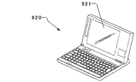
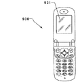
このような構成を採る発光装置1は、デジタルカメラ、パーソナルコンピュータ、又は携帯電話等の表示装置の表示部(ディスプレイ)として用いられる。具体的には、デジタルカメラ910は、例えば図16及び図17のように、操作部911と、表示部912と、を備える。この表示部912に発光装置1が用いられる。同様に、パーソナルコンピュータ920は図18に示すように、表示部921を備え、発光装置1は表示部921に使用される。更に、図19に示すように、携帯電話930は表示部931を備え、発光装置1は表示部931に使用される。
The light emitting device 1 having such a configuration is used as a display unit (display) of a display device such as a digital camera, a personal computer, or a mobile phone. Specifically, the
なお、上記では、理解が容易になるように、発光画素(言い換えると、発光素子)の数を少なくして説明したが、実際の発光素子の数は、もっと多い。 In the above description, the number of light-emitting pixels (in other words, light-emitting elements) is reduced to facilitate understanding, but the actual number of light-emitting elements is larger.
上記実施形態においては、発光装置1は、発光層300が出射する光を基材110側から外部に出射する所謂ボトムエミッション型の発光装置であるとして説明した。しかし、発光装置1は、例えば、発光層300が出射する光を基材110側から外部に出射するトップエミッション型の発光装置であってもよい。また、上記実施形態におけるインクの塗布方法(印刷方法)は、上記ノズルプリンティング等に限らず、例えば、活版印刷、フレキソ印刷等の凸版印刷法、オフセット印刷等の平板印刷、グラビア印刷等の凹版印刷、スクリーン印刷等の孔版印刷等であってもよい。また、本実施形態における発光装置1は、表示装置に使用することができる構成を採用している。しかし、発光装置1は、例えば、プリンタの感光ドラムに光を照射するプリンタヘッド等の露光装置として使用できる構成を採用してもよい。
In the said embodiment, the light-emitting device 1 demonstrated as what is called a bottom emission type light-emitting device which radiate | emits the light which the
1・・・発光装置、9・・・プラズマ照射装置、100・・・基板、110・・・基材、120・・・積層体、121・・・配線、122・・・トランジスタ、122g・・・ゲート電極、122s・・・ソース電極、122d・・・ドレイン電極、123・・・絶縁膜、124・・・ストッパ膜、125・・・半導体層、126,127・・・オーミックコンタクト層、129・・・画素電極、200・・・隔壁、201,251・・・開口部、220・・・第1隔壁、230・・・第2隔壁、250・・・層間絶縁膜、300,399・・・発光層、301,302・・・液面、310・・・中心層、330・・・正孔注入層、350・・・インターレイヤ、400・・・対向電極、910・・・デジタルカメラ、911・・・操作部、912・・・表示部、920・・・ノートパソコン、921・・・表示部、930・・・携帯電話機、931・・・表示部 DESCRIPTION OF SYMBOLS 1 ... Light-emitting device, 9 ... Plasma irradiation apparatus, 100 ... Board | substrate, 110 ... Base material, 120 ... Laminated body, 121 ... Wiring, 122 ... Transistor, 122g ... Gate electrode, 122s ... source electrode, 122d ... drain electrode, 123 ... insulating film, 124 ... stopper film, 125 ... semiconductor layer, 126, 127 ... ohmic contact layer, 129 ... Pixel electrode, 200 ... Partition, 201,251 ... Opening, 220 ... First partition, 230 ... Second partition, 250 ... Interlayer insulating film, 300,399 ... -Light emitting layer, 301, 302 ... Liquid surface, 310 ... Center layer, 330 ... Hole injection layer, 350 ... Interlayer, 400 ... Counter electrode, 910 ... Digital camera, 911 ... operation unit, 12 ... display unit, 920 ... laptops, 921 ... display unit, 930 ... mobile phone, 931 ... display unit
Claims (6)
前記基板上にストライプ状に形成された一対の第1隔壁と、
前記基板上に形成され、前記第1隔壁の長手方向における前記一対の第1隔壁の一端同士を繋ぐ第2隔壁と、
前記基板と前記一対の第1隔壁と前記第2隔壁とによって形成される溝に形成された発光層と、
を備え、
前記第2隔壁の撥液度が、前記長手方向における前記第1隔壁の中央の撥液度よりも低いことを特徴とする発光装置。 A substrate,
A pair of first barrier ribs formed in stripes on the substrate;
A second partition formed on the substrate and connecting one ends of the pair of first partitions in the longitudinal direction of the first partition;
A light emitting layer formed in a groove formed by the substrate, the pair of first barrier ribs, and the second barrier ribs;
With
The light emitting device, wherein the liquid repellency of the second partition is lower than the liquid repellency at the center of the first partition in the longitudinal direction.
前記発光装置は、基板と、前記基板上にストライプ状に形成された一対の第1隔壁と、前記基板上に形成され、前記第1隔壁の長手方向における前記一対の第1隔壁の一端同士を繋ぐ第2隔壁と、前記基板と前記一対の第1隔壁と前記第2隔壁とによって形成される溝に形成された発光層と、を備え、
前記第2隔壁の撥液度を、前記長手方向における前記第1隔壁の中央の撥液度よりも低くするステップを備えることを特徴とする発光装置の製造方法。 A method of manufacturing a light emitting device,
The light emitting device includes a substrate, a pair of first partitions formed in a stripe shape on the substrate, and one end of the pair of first partitions formed in the longitudinal direction of the first partition. A second partition wall to be connected; and a light emitting layer formed in a groove formed by the substrate, the pair of first partition walls, and the second partition wall;
A method for manufacturing a light emitting device, comprising: making the liquid repellency of the second partition wall lower than the liquid repellency of the center of the first partition wall in the longitudinal direction.
Priority Applications (5)
| Application Number | Priority Date | Filing Date | Title |
|---|---|---|---|
| JP2009180187A JP2011034814A (en) | 2009-07-31 | 2009-07-31 | Light-emitting device, display device, and manufacturing method of light-emitting device |
| KR1020100073124A KR20110013289A (en) | 2009-07-31 | 2010-07-29 | Light emitting device, display device, and method of manufacturing light emitting device |
| US12/846,881 US8282436B2 (en) | 2009-07-31 | 2010-07-30 | Light emitting device, electronic device, and method of manufacturing light emitting device |
| CN201010243496.7A CN101989648B (en) | 2009-07-31 | 2010-07-30 | Light emitting device, electronic device, and method of manufacturing light emitting device |
| TW099125232A TWI439168B (en) | 2009-07-31 | 2010-07-30 | A method for manufacturing light emitting device |
Applications Claiming Priority (1)
| Application Number | Priority Date | Filing Date | Title |
|---|---|---|---|
| JP2009180187A JP2011034814A (en) | 2009-07-31 | 2009-07-31 | Light-emitting device, display device, and manufacturing method of light-emitting device |
Publications (2)
| Publication Number | Publication Date |
|---|---|
| JP2011034814A true JP2011034814A (en) | 2011-02-17 |
| JP2011034814A5 JP2011034814A5 (en) | 2011-04-07 |
Family
ID=43526320
Family Applications (1)
| Application Number | Title | Priority Date | Filing Date |
|---|---|---|---|
| JP2009180187A Pending JP2011034814A (en) | 2009-07-31 | 2009-07-31 | Light-emitting device, display device, and manufacturing method of light-emitting device |
Country Status (5)
| Country | Link |
|---|---|
| US (1) | US8282436B2 (en) |
| JP (1) | JP2011034814A (en) |
| KR (1) | KR20110013289A (en) |
| CN (1) | CN101989648B (en) |
| TW (1) | TWI439168B (en) |
Cited By (1)
| Publication number | Priority date | Publication date | Assignee | Title |
|---|---|---|---|---|
| WO2013111300A1 (en) * | 2012-01-26 | 2013-08-01 | パイオニア株式会社 | Organic el panel and method for manufacturing same |
Families Citing this family (10)
| Publication number | Priority date | Publication date | Assignee | Title |
|---|---|---|---|---|
| CN103164791B (en) * | 2011-12-13 | 2016-04-06 | 阿里巴巴集团控股有限公司 | A kind of method and apparatus being realized secure payment by electric terminal |
| WO2013116779A1 (en) * | 2012-02-01 | 2013-08-08 | Futurewei Technologies, Inc. | System and method for organizing multimedia content |
| KR101924606B1 (en) * | 2012-04-27 | 2018-12-04 | 삼성디스플레이 주식회사 | Organic light emitting display device and the fabrication method thereof |
| US20130346301A1 (en) * | 2012-06-22 | 2013-12-26 | Paychief Llc. | Systems and methods for billing via a symbology |
| JP2014222642A (en) * | 2013-05-14 | 2014-11-27 | 三星ディスプレイ株式會社Samsung Display Co.,Ltd. | Manufacturing method and manufacturing apparatus of organic el display device |
| CN104599121B (en) * | 2013-10-30 | 2017-04-12 | 腾讯科技(深圳)有限公司 | Information transmission method, device and system |
| US9799711B2 (en) * | 2014-03-04 | 2017-10-24 | Joled Inc. | Organic EL display panel and organic EL display device |
| CN108251846A (en) * | 2018-01-12 | 2018-07-06 | 大连理工大学 | A kind of method that no mask prepares patterned wettability surface |
| KR20200073599A (en) * | 2018-12-14 | 2020-06-24 | 엘지디스플레이 주식회사 | Electroluminescent Device |
| KR102268603B1 (en) * | 2019-07-10 | 2021-06-22 | 세메스 주식회사 | Substrate, display panel and substrate manufacturing method |
Citations (9)
| Publication number | Priority date | Publication date | Assignee | Title |
|---|---|---|---|---|
| JP2007087785A (en) * | 2005-09-22 | 2007-04-05 | Toppan Printing Co Ltd | Manufacturing method of printing body, and printing body |
| JP2008010221A (en) * | 2006-06-28 | 2008-01-17 | Dainippon Screen Mfg Co Ltd | Tape peeling device, application system, and tape peeling method |
| JP2009026671A (en) * | 2007-07-23 | 2009-02-05 | Seiko Epson Corp | Electro-optical device, manufacturing method thereof, and electronic apparatus |
| JP2009070767A (en) * | 2007-09-18 | 2009-04-02 | Casio Comput Co Ltd | Method of manufacturing display device |
| JP2009070899A (en) * | 2007-09-11 | 2009-04-02 | Sharp Corp | Plasma processing device and plasma processing method |
| JP2009075194A (en) * | 2007-09-19 | 2009-04-09 | Casio Comput Co Ltd | Display panel and manufacturing method |
| JP2009170434A (en) * | 2001-12-18 | 2009-07-30 | Seiko Epson Corp | Display |
| JP2010080086A (en) * | 2008-09-24 | 2010-04-08 | Sumitomo Chemical Co Ltd | Base board for pattern coating and organic el element |
| JP2010176938A (en) * | 2009-01-28 | 2010-08-12 | Seiko Epson Corp | Electrooptical device, method of manufacturing the same, and electronic apparatus |
Family Cites Families (8)
| Publication number | Priority date | Publication date | Assignee | Title |
|---|---|---|---|---|
| JP3328297B2 (en) | 1998-03-17 | 2002-09-24 | セイコーエプソン株式会社 | Display device manufacturing method |
| JP2002075640A (en) | 2000-08-30 | 2002-03-15 | Dainippon Screen Mfg Co Ltd | Manufacturing method of an organic el display device and its manufacturing device |
| US6852524B2 (en) * | 2001-04-27 | 2005-02-08 | Canon Kabushiki Kaisha | Probe carrier, probe fixing carrier and method of manufacturing the same |
| JP5105877B2 (en) * | 2004-10-13 | 2012-12-26 | シャープ株式会社 | Functional board |
| EP1666258B1 (en) * | 2004-12-01 | 2011-10-05 | FUJIFILM Corporation | Repellency increasing structure and method of producing the same, liquid ejection head and method of producing the same, and stain-resistant film |
| JP2006286309A (en) * | 2005-03-31 | 2006-10-19 | Toppan Printing Co Ltd | Organic electroluminescent display device and its manufacturing method |
| JP4175397B2 (en) * | 2006-06-28 | 2008-11-05 | セイコーエプソン株式会社 | Method for manufacturing organic electroluminescent device |
| JP4888268B2 (en) * | 2007-07-23 | 2012-02-29 | セイコーエプソン株式会社 | Electro-optical device and electronic apparatus |
-
2009
- 2009-07-31 JP JP2009180187A patent/JP2011034814A/en active Pending
-
2010
- 2010-07-29 KR KR1020100073124A patent/KR20110013289A/en not_active Application Discontinuation
- 2010-07-30 TW TW099125232A patent/TWI439168B/en not_active IP Right Cessation
- 2010-07-30 CN CN201010243496.7A patent/CN101989648B/en not_active Expired - Fee Related
- 2010-07-30 US US12/846,881 patent/US8282436B2/en active Active
Patent Citations (9)
| Publication number | Priority date | Publication date | Assignee | Title |
|---|---|---|---|---|
| JP2009170434A (en) * | 2001-12-18 | 2009-07-30 | Seiko Epson Corp | Display |
| JP2007087785A (en) * | 2005-09-22 | 2007-04-05 | Toppan Printing Co Ltd | Manufacturing method of printing body, and printing body |
| JP2008010221A (en) * | 2006-06-28 | 2008-01-17 | Dainippon Screen Mfg Co Ltd | Tape peeling device, application system, and tape peeling method |
| JP2009026671A (en) * | 2007-07-23 | 2009-02-05 | Seiko Epson Corp | Electro-optical device, manufacturing method thereof, and electronic apparatus |
| JP2009070899A (en) * | 2007-09-11 | 2009-04-02 | Sharp Corp | Plasma processing device and plasma processing method |
| JP2009070767A (en) * | 2007-09-18 | 2009-04-02 | Casio Comput Co Ltd | Method of manufacturing display device |
| JP2009075194A (en) * | 2007-09-19 | 2009-04-09 | Casio Comput Co Ltd | Display panel and manufacturing method |
| JP2010080086A (en) * | 2008-09-24 | 2010-04-08 | Sumitomo Chemical Co Ltd | Base board for pattern coating and organic el element |
| JP2010176938A (en) * | 2009-01-28 | 2010-08-12 | Seiko Epson Corp | Electrooptical device, method of manufacturing the same, and electronic apparatus |
Cited By (1)
| Publication number | Priority date | Publication date | Assignee | Title |
|---|---|---|---|---|
| WO2013111300A1 (en) * | 2012-01-26 | 2013-08-01 | パイオニア株式会社 | Organic el panel and method for manufacturing same |
Also Published As
| Publication number | Publication date |
|---|---|
| CN101989648B (en) | 2014-10-01 |
| US8282436B2 (en) | 2012-10-09 |
| TW201117639A (en) | 2011-05-16 |
| CN101989648A (en) | 2011-03-23 |
| US20110025189A1 (en) | 2011-02-03 |
| TWI439168B (en) | 2014-05-21 |
| KR20110013289A (en) | 2011-02-09 |
Similar Documents
| Publication | Publication Date | Title |
|---|---|---|
| JP2011034814A (en) | Light-emitting device, display device, and manufacturing method of light-emitting device | |
| JP4547038B2 (en) | Organic EL display panel and manufacturing method thereof | |
| US7777411B2 (en) | Light-emitting device, method of producing light-emitting device, exposure unit, and electronic device | |
| JP4540747B2 (en) | Organic EL device and organic EL display panel | |
| JP4374073B2 (en) | Organic EL display panel | |
| JP4333728B2 (en) | Electro-optical device manufacturing method and electronic apparatus | |
| US8154032B2 (en) | Electrooptical device, electronic apparatus, and method for producing electrooptical device | |
| JP2010050107A (en) | Organic el display panel | |
| JP2011103222A (en) | Organic el element, method of manufacturing the same, organic el device, and electronic equipment | |
| JP4811292B2 (en) | Manufacturing method of display device | |
| JP2005203215A (en) | Organic el element | |
| JP5201484B2 (en) | LIGHT EMITTING DEVICE, ITS MANUFACTURING METHOD, AND ELECTRONIC DEVICE | |
| JP2006004743A (en) | Display device and its manufacturing method | |
| JP4760168B2 (en) | Display panel and manufacturing method thereof | |
| JP6083122B2 (en) | Organic electroluminescence device and method for manufacturing the same | |
| JP4710847B2 (en) | Manufacturing method of display device | |
| JP2008004378A (en) | Device, thin-film forming method, manufacturing method of device, and electronic equipment | |
| JP4930303B2 (en) | Manufacturing method of display device | |
| JP4940831B2 (en) | Method for manufacturing organic EL element and organic EL element | |
| JP5056476B2 (en) | Display device and manufacturing method of display device | |
| JP2010040816A (en) | Organic el device, manufacturing method of the organic el device, and electronic apparatus | |
| JP2011187364A (en) | Organic electroluminescent element and method of manufacturing the same | |
| JP5515488B2 (en) | LIGHT EMITTING DEVICE, LIGHT EMITTING DEVICE MANUFACTURING METHOD, AND ELECTRONIC DEVICE |
Legal Events
| Date | Code | Title | Description |
|---|---|---|---|
| A521 | Request for written amendment filed |
Free format text: JAPANESE INTERMEDIATE CODE: A523 Effective date: 20110217 |
|
| A621 | Written request for application examination |
Free format text: JAPANESE INTERMEDIATE CODE: A621 Effective date: 20110217 |
|
| A977 | Report on retrieval |
Free format text: JAPANESE INTERMEDIATE CODE: A971007 Effective date: 20110511 |
|
| A131 | Notification of reasons for refusal |
Free format text: JAPANESE INTERMEDIATE CODE: A131 Effective date: 20110517 |
|
| A521 | Request for written amendment filed |
Free format text: JAPANESE INTERMEDIATE CODE: A523 Effective date: 20110719 |
|
| A131 | Notification of reasons for refusal |
Free format text: JAPANESE INTERMEDIATE CODE: A131 Effective date: 20110802 |
|
| A02 | Decision of refusal |
Free format text: JAPANESE INTERMEDIATE CODE: A02 Effective date: 20111129 |