KR20080098368A - High cell density trench MOSFETs with varying mesa dimensions - Google Patents
High cell density trench MOSFETs with varying mesa dimensions Download PDFInfo
- Publication number
- KR20080098368A KR20080098368A KR1020087019275A KR20087019275A KR20080098368A KR 20080098368 A KR20080098368 A KR 20080098368A KR 1020087019275 A KR1020087019275 A KR 1020087019275A KR 20087019275 A KR20087019275 A KR 20087019275A KR 20080098368 A KR20080098368 A KR 20080098368A
- Authority
- KR
- South Korea
- Prior art keywords
- cells
- cell
- trench gate
- trench
- width
- Prior art date
- Legal status (The legal status is an assumption and is not a legal conclusion. Google has not performed a legal analysis and makes no representation as to the accuracy of the status listed.)
- Granted
Links
Images


Classifications
-
- H—ELECTRICITY
- H10—SEMICONDUCTOR DEVICES; ELECTRIC SOLID-STATE DEVICES NOT OTHERWISE PROVIDED FOR
- H10D—INORGANIC ELECTRIC SEMICONDUCTOR DEVICES
- H10D30/00—Field-effect transistors [FET]
- H10D30/60—Insulated-gate field-effect transistors [IGFET]
- H10D30/64—Double-diffused metal-oxide semiconductor [DMOS] FETs
- H10D30/66—Vertical DMOS [VDMOS] FETs
- H10D30/668—Vertical DMOS [VDMOS] FETs having trench gate electrodes, e.g. UMOS transistors
-
- H—ELECTRICITY
- H10—SEMICONDUCTOR DEVICES; ELECTRIC SOLID-STATE DEVICES NOT OTHERWISE PROVIDED FOR
- H10P—GENERIC PROCESSES OR APPARATUS FOR THE MANUFACTURE OR TREATMENT OF DEVICES COVERED BY CLASS H10
- H10P10/00—Bonding of wafers, substrates or parts of devices
-
- H—ELECTRICITY
- H10—SEMICONDUCTOR DEVICES; ELECTRIC SOLID-STATE DEVICES NOT OTHERWISE PROVIDED FOR
- H10D—INORGANIC ELECTRIC SEMICONDUCTOR DEVICES
- H10D12/00—Bipolar devices controlled by the field effect, e.g. insulated-gate bipolar transistors [IGBT]
- H10D12/01—Manufacture or treatment
-
- H—ELECTRICITY
- H10—SEMICONDUCTOR DEVICES; ELECTRIC SOLID-STATE DEVICES NOT OTHERWISE PROVIDED FOR
- H10D—INORGANIC ELECTRIC SEMICONDUCTOR DEVICES
- H10D12/00—Bipolar devices controlled by the field effect, e.g. insulated-gate bipolar transistors [IGBT]
- H10D12/01—Manufacture or treatment
- H10D12/031—Manufacture or treatment of IGBTs
- H10D12/032—Manufacture or treatment of IGBTs of vertical IGBTs
- H10D12/038—Manufacture or treatment of IGBTs of vertical IGBTs having a recessed gate, e.g. trench-gate IGBTs
-
- H—ELECTRICITY
- H10—SEMICONDUCTOR DEVICES; ELECTRIC SOLID-STATE DEVICES NOT OTHERWISE PROVIDED FOR
- H10D—INORGANIC ELECTRIC SEMICONDUCTOR DEVICES
- H10D12/00—Bipolar devices controlled by the field effect, e.g. insulated-gate bipolar transistors [IGBT]
- H10D12/411—Insulated-gate bipolar transistors [IGBT]
- H10D12/441—Vertical IGBTs
- H10D12/461—Vertical IGBTs having non-planar surfaces, e.g. having trenches, recesses or pillars in the surfaces of the emitter, base or collector regions
- H10D12/481—Vertical IGBTs having non-planar surfaces, e.g. having trenches, recesses or pillars in the surfaces of the emitter, base or collector regions having gate structures on slanted surfaces, on vertical surfaces, or in grooves, e.g. trench gate IGBTs
-
- H—ELECTRICITY
- H10—SEMICONDUCTOR DEVICES; ELECTRIC SOLID-STATE DEVICES NOT OTHERWISE PROVIDED FOR
- H10D—INORGANIC ELECTRIC SEMICONDUCTOR DEVICES
- H10D30/00—Field-effect transistors [FET]
- H10D30/01—Manufacture or treatment
- H10D30/021—Manufacture or treatment of FETs having insulated gates [IGFET]
- H10D30/028—Manufacture or treatment of FETs having insulated gates [IGFET] of double-diffused metal oxide semiconductor [DMOS] FETs
- H10D30/0291—Manufacture or treatment of FETs having insulated gates [IGFET] of double-diffused metal oxide semiconductor [DMOS] FETs of vertical DMOS [VDMOS] FETs
- H10D30/0295—Manufacture or treatment of FETs having insulated gates [IGFET] of double-diffused metal oxide semiconductor [DMOS] FETs of vertical DMOS [VDMOS] FETs using recessing of the source electrodes
-
- H—ELECTRICITY
- H10—SEMICONDUCTOR DEVICES; ELECTRIC SOLID-STATE DEVICES NOT OTHERWISE PROVIDED FOR
- H10D—INORGANIC ELECTRIC SEMICONDUCTOR DEVICES
- H10D30/00—Field-effect transistors [FET]
- H10D30/01—Manufacture or treatment
- H10D30/021—Manufacture or treatment of FETs having insulated gates [IGFET]
- H10D30/028—Manufacture or treatment of FETs having insulated gates [IGFET] of double-diffused metal oxide semiconductor [DMOS] FETs
- H10D30/0291—Manufacture or treatment of FETs having insulated gates [IGFET] of double-diffused metal oxide semiconductor [DMOS] FETs of vertical DMOS [VDMOS] FETs
- H10D30/0297—Manufacture or treatment of FETs having insulated gates [IGFET] of double-diffused metal oxide semiconductor [DMOS] FETs of vertical DMOS [VDMOS] FETs using recessing of the gate electrodes, e.g. to form trench gate electrodes
-
- H—ELECTRICITY
- H10—SEMICONDUCTOR DEVICES; ELECTRIC SOLID-STATE DEVICES NOT OTHERWISE PROVIDED FOR
- H10D—INORGANIC ELECTRIC SEMICONDUCTOR DEVICES
- H10D84/00—Integrated devices formed in or on semiconductor substrates that comprise only semiconducting layers, e.g. on Si wafers or on GaAs-on-Si wafers
- H10D84/101—Integrated devices comprising main components and built-in components, e.g. IGBT having built-in freewheel diode
- H10D84/141—VDMOS having built-in components
- H10D84/148—VDMOS having built-in components the built-in components being breakdown diodes, e.g. Zener diodes
-
- H—ELECTRICITY
- H10—SEMICONDUCTOR DEVICES; ELECTRIC SOLID-STATE DEVICES NOT OTHERWISE PROVIDED FOR
- H10D—INORGANIC ELECTRIC SEMICONDUCTOR DEVICES
- H10D64/00—Electrodes of devices having potential barriers
- H10D64/20—Electrodes characterised by their shapes, relative sizes or dispositions
- H10D64/27—Electrodes not carrying the current to be rectified, amplified, oscillated or switched, e.g. gates
- H10D64/311—Gate electrodes for field-effect devices
- H10D64/411—Gate electrodes for field-effect devices for FETs
- H10D64/511—Gate electrodes for field-effect devices for FETs for IGFETs
- H10D64/512—Disposition of the gate electrodes, e.g. buried gates
- H10D64/513—Disposition of the gate electrodes, e.g. buried gates within recesses in the substrate, e.g. trench gates, groove gates or buried gates
-
- H—ELECTRICITY
- H10—SEMICONDUCTOR DEVICES; ELECTRIC SOLID-STATE DEVICES NOT OTHERWISE PROVIDED FOR
- H10D—INORGANIC ELECTRIC SEMICONDUCTOR DEVICES
- H10D64/00—Electrodes of devices having potential barriers
- H10D64/20—Electrodes characterised by their shapes, relative sizes or dispositions
- H10D64/27—Electrodes not carrying the current to be rectified, amplified, oscillated or switched, e.g. gates
- H10D64/311—Gate electrodes for field-effect devices
- H10D64/411—Gate electrodes for field-effect devices for FETs
- H10D64/511—Gate electrodes for field-effect devices for FETs for IGFETs
- H10D64/517—Gate electrodes for field-effect devices for FETs for IGFETs characterised by the conducting layers
Landscapes
- Electrodes Of Semiconductors (AREA)
- Metal-Oxide And Bipolar Metal-Oxide Semiconductor Integrated Circuits (AREA)
Abstract
낮은 핀치 베이스 저항을 유지하면서 높은 전류 운반 성능을 위한 높은 셀 밀도를 갖는 전력 모스펫을 위한 회로, 방법 및 장치가 제공된다. 일 디바이스는 다양한 메사(트랜치 게이트들 사이의 영역) 크기를 갖는 다수의 트랜지스터 셀을 사용한다. 핀치 상태 베이스 저항을 감소시키기 위해 더 큰 셀 내에 고농도 본체 식각이 이용된다. 이 식각은 메사 영역 내의 실리콘을 제거하는데, 상기 실리콘은 보다 낮은 임피던스의 알루미늄으로 대체된다. 디바이스 전류 용량을 증가시키기 위해, 상기 식각을 받지 않는 다수의 더 작은 메사 셀이 이용된다. 이들 셀이 더 낮은 BVDSS 항복 전압을 갖는다는 것을 보장함으로써, 전자 사태(avalanche) 전류는 크기가 더 크고 핀치 베이스가 더 낮은 셀을 향한다. 큰 셀의 BVDSS는 임계 치수(critical dimension), 즉, 폭이 더 넓은 메사의 양측의 트랜치 게이트들의 폭을 조정하거나, 또는 상기 고농도 본체 식각의 깊이를 조정함으로써 변동될 수 있다. Circuits, methods, and apparatus are provided for power MOSFETs having high cell density for high current carrying performance while maintaining low pinch base resistance. One device uses multiple transistor cells with various mesas (regions between trench gates). High concentration body etching is used in larger cells to reduce pinch state base resistance. This etching removes silicon in the mesa region, which is replaced by lower impedance aluminum. In order to increase device current capacity, a number of smaller mesa cells that do not receive the etch are used. By ensuring that these cells have a lower BVDSS breakdown voltage, the avalanche currents are directed towards cells of larger magnitude and lower pinch base. Large cell BVDSS can be varied by adjusting the critical dimension, ie the width of the trench gates on either side of the wider mesa, or by adjusting the depth of the high concentration body etch.
Description
본 발명은 일반적으로 전력 모스펫(MOSFET) 트랜지스터에 관한 것이고, 보다 구체적으로는, 다양한 메사 치수를 갖는 전력 모스펫 트랜지스터에 관한 것이다. The present invention relates generally to power MOSFET transistors, and more particularly to power MOSFET transistors having various mesa dimensions.
전력 모스펫(MOSFET)의 이용은 빠르게 보편화되고 있으며, 점점 더 많은 수의 응용 제품들 내에 장착되도록 요구됨에 따라, 향후 수년 내에 더욱 대중적으로 될 것이 분명하다. 그러나, 이러한 응용 제품들에 대한 요구는 이들 디바이스의 성능에 부담을 주고 있다. 이에 따라, 향상된 성능을 갖는 전력 모스펫 디바이스가 요구된다. The use of power MOSFETs is quickly becoming common and will be increasingly popular in the next few years as it is required to be mounted in an increasing number of applications. However, the demand for these applications places a strain on the performance of these devices. Accordingly, there is a need for a power MOSFET device with improved performance.
일반적인 동작 중에, 도전 상태가 될 때 전력 모스펫은 인덕터를 통해 전류를 끌어당긴다. 상기 전력 모스펫이 오프(off) 상태가 될 때, 상기 인덕터가 저장된 에너지를 유지한다. 이 저장된 에너지는 인덕터를 통해 전류를 발생시키는데, 상기 전류는 인덕터의 양호도(quality factor), 즉, "Q"의 함수로서 시간이 경과함에 따라 감소한다. 상기 전류는 디바이스가 전자 사태 항복 모드(avalanche breakdown mode)로 진입할 때, 상기 전력 모스펫 내에서 소모된다. During normal operation, the power MOSFET draws current through the inductor when in a conductive state. When the power MOSFET is turned off, the inductor maintains stored energy. This stored energy generates a current through the inductor, which decreases over time as a function of the inductor's quality factor, i.e., "Q". The current is dissipated in the power MOSFET when the device enters an avalanche breakdown mode.
전자 사태 전류는 전력 모스펫 디바이스의 본체 다이오드, 즉, 드레인과 웰 영역 사이의 접합부를 거쳐 상기 전력 모스펫 디바이스를 통과한다. n-채널 트랜지스터에 있어서, 전자 사태 전류는 N-타입 드레인으로부터 P-웰을 통해 고농도 본체 접촉부로 흐른다. 상기 트랜지스터는 이 전류를 처리하도록 설계되므로, 이러한 동작은 해를 끼치지 않는다. The avalanche current passes through the power MOSFET device via a body diode of the power MOSFET device, i.e., the junction between the drain and the well region. In n-channel transistors, the avalanche current flows from the N-type drain through the P-well to the high concentration body contacts. Since the transistor is designed to handle this current, this operation is not harmful.
그러나, 만약 웰-소스 간 다이오드가 온(on) 상태가 된다면, 2차적인 기생 양극성 동작이 시작될 수 있다. 이러한 2차적인 양극성 동작은 디바이스에 해를 끼칠 수 있는 폭주 전류(runaway current)를 발생시킬 수 있다. 상기 웰-소스 간 다이오드는, 웰 저항이 과도하다면, 즉, 핀치 베이스(pinched-base) 저항이 너무 높다면, 온 상태가 될 수 있다. However, if the well-source diode is turned on, secondary parasitic bipolar operation may begin. This secondary bipolar operation can generate runaway currents that can harm the device. The well-source diode may be turned on if the well resistance is excessive, that is, if the pinched-base resistance is too high.
따라서, 2차적인 양극성 동작을 방지하기 위해, 핀치 베이스 저항을 감소시키는 것이 바람직하다. 그러나, 이 저항을 감소시키는 많은 기술들은 셀 크기를 증가시킨다. 더욱 큰 셀 크기는 집적될 수 있는 셀의 개수를 감소시키고, 디바이스 전류 운반 능력을 감소시킨다. Thus, to prevent secondary bipolar operation, it is desirable to reduce the pinch base resistance. However, many techniques for reducing this resistance increase cell size. Larger cell sizes reduce the number of cells that can be integrated and reduce device current carrying capacity.
그러므로, 낮은 핀치 베이스 저항을 유지하면서 많은 수의 셀을 포함하는 전력 모스펫을 제공하는 회로, 방법 및 장치가 요구된다. Therefore, what is needed is a circuit, method and apparatus for providing a power MOSFET containing a large number of cells while maintaining a low pinch base resistance.
따라서, 본 발명의 실시예들은, 낮은 핀치 베이스 저항을 유지하면서 높은 전류 운반 성능을 위한 높은 셀 밀도를 갖는 전력 디바이스를 위한 회로, 방법 및 장치를 제공한다. Accordingly, embodiments of the present invention provide circuits, methods, and apparatus for power devices having high cell density for high current carrying performance while maintaining low pinch base resistance.
본 발명의 예시적인 실시예는 다양한 메사(mesa) 크기를 갖는 다수의 트랜지스터 셀을 사용한다. 메사는 트랜치 전력 모스펫 트랜지스터의 소스 영역인데, 다시 말해, 메사는 트랜치 게이트들 사이의 영역이다. 특정한 일 실시예는 셀에 대해 두 가지 크기의 메사를 이용하지만, 다른 실시예들은 둘 이상의 크기를 이용할 수 있다. Exemplary embodiments of the present invention use multiple transistor cells having various mesa sizes. The mesa is the source region of the trench power MOSFET transistors, that is, the mesa is the region between the trench gates. One particular embodiment uses two sizes of mesas for the cell, while other embodiments may use more than one size.
본 발명의 특정 실시예는, 트랜치-게이트 전력 모스펫(trench-gate power MOSFET)의 핀치 베이스(pinched-base) 저항을 감소시키기 위해 고농도 본체 식각을 이용한다. 이 식각은 메사 영역 내의 실리콘을 제거하고, 상기 실리콘은 보다 낮은 임피던스의 알루미늄으로 대체된다. 그러나, 고농도 본체 식각에 필요한 셀 크기는, 높은 전류 공급 능력을 갖는 디바이스에 이상적인 크기에 비해 더 크다. 따라서, 본 실시예는 또한 이러한 식각을 받지 않는 다수의 더 작은 메사 셀을 이용한다. Certain embodiments of the present invention utilize high concentration body etching to reduce the pinched-base resistance of trench-gate power MOSFETs. This etching removes silicon in the mesa region, which is replaced by lower impedance aluminum. However, the cell size required for high concentration body etching is larger than the ideal size for devices with high current supply capability. Thus, the present embodiment also uses a number of smaller mesa cells that do not receive this etching.
상기 더 작은 메사 셀은 더 높은 핀치 베이스 저항을 갖는다. 따라서, 당해 디바이스에 2차적인 양극성 항복(breakdown)이 나타나는 것을 방지하기 위해, 상기 디바이스의 대부분의 전자 사태 전류(avalanche current)가 크기가 더 크고, 핀치 베이스 저항이 더 낮은 셀을 향하게 한다. 이는 이들 셀이 더 낮은 본체-다이오드 항복(BVDSS) 전압을 갖는다는 것을 보장함으로써 이루어질 수 있다. 구체적으로, 상기 더 큰 셀의 BVDSS는, 요구되는 어떠한 사양(specification)이라도 충족시킬 수 있을 만큼 높지만, 상기 작은 셀의 BVDSS 항복 전압보다는 낮게 만들어진다. 상기 더 큰 셀의 BVDSS는 임계 치수(critical dimension; CD), 즉, 폭이 더 넓은 메사의 양측에 있는 트랜치 게이트의 폭을 조정하거나, 상기 고농도 본체 식각의 깊이를 조정함으로써 변동될 수 있다. The smaller mesa cell has a higher pinch base resistance. Thus, to prevent secondary bipolar breakdown in the device, most of the device's avalanche currents are directed to cells with larger magnitudes and lower pinch base resistances. This can be done by ensuring that these cells have lower body-diode breakdown (BVDSS) voltages. Specifically, the BVDSS of the larger cell is made high enough to meet any required specification, but lower than the BVDSS breakdown voltage of the small cell. The BVDSS of the larger cell can be varied by adjusting the critical dimension (CD), ie the width of the trench gates on either side of the wider mesa, or by adjusting the depth of the high concentration body etch.
전력 모스펫은 요구되는 전자 사태 전류를 처리하기 위해 상기 더 큰 셀을 충분히 포함하도록 설계된다. 요구되는 디바이스 전류 운반 성능을 제공하는데 필요한 수의 상기 추가적인 더 작은 셀들이 추가될 수 있다. 본 발명의 다양한 실시예들이 본 명세서에 기재된 또는 다른 특징들 중 하나 또는 그 이상을 이용할 수 있다. The power MOSFET is designed to include enough of the larger cell to handle the required avalanche current. The additional smaller cells may be added as needed to provide the required device current carrying performance. Various embodiments of the invention may utilize one or more of the features or other features described herein.
본 발명의 본질 및 이점은 이하의 상세한 설명 및 첨부된 도면을 참조함으로써 보다 잘 이해될 수 있다. The nature and advantages of the present invention can be better understood by reference to the following detailed description and the accompanying drawings.
도 1은 본 발명의 실시예에 의해 통합될 수 있는, 고농도 본체 접촉 식각을 포함하는 트랜지스터 셀의 측면도이다. 1 is a side view of a transistor cell including a high concentration body contact etch, which may be incorporated by an embodiment of the present invention.
도 2는 본 발명의 일 실시예에 따른 트랜지스터의 측면도이다. 2 is a side view of a transistor according to an embodiment of the present invention.
도 3은 본 발명의 일 실시예에 따른, 서로 인접한 폭이 좁은 트랜지스터 셀과 폭이 넓은 트랜지스터 셀의 측면도이다. 3 is a side view of a narrow transistor cell and a wide transistor cell adjacent to each other according to an embodiment of the present invention.
도 4A는 디바이스 트랜치 깊이의 변화를 트랜치 게이트 폭의 함수로서 나타낸다.4A shows the change in device trench depth as a function of trench gate width.
도 4B는 항복 전압의 변화를 트랜치 깊이의 함수로서 나타낸다.4B shows the change in breakdown voltage as a function of trench depth.
도 5는 본 발명의 일 실시예에 따른 트랜지스터의 평면도를 도시한다. 5 shows a top view of a transistor in accordance with an embodiment of the present invention.
도 6은 본 발명의 일 실시예에 따른 전력 모스펫 디바이스를 설계하는 방법을 도시하는 흐름도이다. 6 is a flowchart illustrating a method of designing a power MOSFET device according to an embodiment of the present invention.
도 7은 본 발명의 일 실시예에 따른 전력 모스펫 디바이스를 설계하는 방법을 도시하는 다른 흐름도이다. 7 is another flowchart illustrating a method of designing a power MOSFET device according to an embodiment of the present invention.
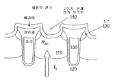
도 1은 본 발명의 실시예에 의해 통합될 수 있는, 고농도 본체 접촉 식각을 포함하는 트랜지스터 셀의 측면도이다. 당해 디바이스는 본체 또는 벌크(bulk) 영역 110, 드레인 120 및 소스 영역 130을 포함한다. 1 is a side view of a transistor cell including a high concentration body contact etch, which may be incorporated by an embodiment of the present invention. The device includes a body or
일반적으로, 도 1에 도시된 트랜지스터가 온(on) 상태가 되고 도전 상태가 될 때, 상기 트랜지스터는 인덕터를 통해 전류를 끌어당긴다. 상기 트랜지스터가 오프(off) 상태가 될 때, 상기 인덕터에 저장된 에너지는 전류 I0로 도시된 전류를 발생시키고, 이 전류는 디바이스를 통해 흐른다. 이 전류는 본체 다이오드 내에 전자 사태 항복(avalanche breakdown)을 일으킨다. 본 발명의 실시예에서, 이러한 항복은 해를 끼치지 않고, 상기 트랜지스터는 이 전류를 처리하도록 설계된다. Generally, when the transistor shown in FIG. 1 is turned on and in a conductive state, the transistor draws current through the inductor. When the transistor is off, the energy stored in the inductor generates a current, shown as current I 0 , which flows through the device. This current causes an avalanche breakdown in the body diode. In an embodiment of the invention, this breakdown is harmless and the transistor is designed to handle this current.
그러나, 핀치 베이스(pinched base) 저항이 과도하게 되면, 웰-소스 간 다이오드는 순방향 바이어스(forward bias)될 수 있으며, 상당한 양의 전류를 통과시키 기 시작한다. 이 다이오드는 양극성 트랜지스터의 이미터(emitter)로서 동작한다. 이러한 2차적인 양극성 효과로 인해 야기되는 전류는 제어되지 않으며, 디바이스에 해를 끼칠 만큼 커질 수 있다. 웰-소스 간 다이오드가 정방향 바이어스되는 것을 방지하기 위해, 상기 디바이스는 도 1에 도시된 바와 같이 핀치 베이스 저항을 감소시키는 고농도 본체 접촉 식각을 이용하여 개선된다. However, if the pinched base resistance becomes excessive, the well-source-to-source diode may be forward biased and begin to pass a significant amount of current. This diode acts as an emitter of the bipolar transistor. The current caused by this secondary bipolar effect is not controlled and can be large enough to harm the device. To prevent the well-sourced diodes from being forward biased, the device is improved using a high concentration body contact etch that reduces the pinch base resistance as shown in FIG.
구체적으로, 영역 110 내의 본체의 일부분이 고농도 본체 접촉 식각 140에 의해 제거된다. 이러한 접근 방법은, 메사로부터 실리콘 물질을 제거하는 단계 및 알루미늄과 같이 저항이 더 낮은 물질로 상기 실리콘 물질을 대체하는 단계를 포함한다. Specifically, a portion of the body in
이 방법은, 상기 디바이스의 핀치 베이스 저항을 감소시킴에 있어서 효과적이다. 그러나, 고농도 본체 접촉 식각은 폭이 더 넓은 메사 디바이스를 요구하고, 이로써 주어진 디바이스 크기 내의 전체 셀의 개수를 감소시킨다. 그러나, 전류 운반 성능을 증가시키기 위해, 즉, 온 저항(on resistance)을 감소시키기 위해서는 디바이스 내에 많은 수의 셀을 포함하는 것이 바람직하다. 따라서 본 발명의 일 실시예는, 낮은 온 저항, 즉, 온 상태가 되고 도전 상태가 된 때의 높은 전류 운반 성능을 위해, 디바이스 내의 전체 셀의 개수를 증가시키도록 폭이 더 좁은 셀을 추가로 이용하는 한편, 인덕터 턴-오프(turn-off) 전류를 처리하는데 필요한 수의 폭이 더 넓은 셀을 이용한다. This method is effective in reducing the pinch base resistance of the device. However, high concentration body contact etching requires a wider mesa device, thereby reducing the total number of cells within a given device size. However, it is desirable to include a large number of cells in the device to increase current carrying performance, i.e. to reduce on resistance. Thus, one embodiment of the present invention further provides a narrower cell to provide a lower on-resistance, i.e., higher current carrying performance when turned on and in a conductive state, to increase the total number of cells in the device. On the other hand, it uses a wider number of cells needed to handle inductor turn-off current.
도 2는, 높은 셀 밀도를 제공하는 동시에, 식각된 고농도 본체의 낮은 베이 스 저항 R bb' 을 이용하는, 서로 다른 두 개의 메사 크기를 갖는 셀 구조물을 도시한다. 이 도면은 폭이 넓은 셀 210과 다수의 폭이 더 좁은 셀 220을 포함한다. 상기 폭이 넓은 셀 210 내의 메사의 치수는 고농도 본체 접촉 식각이 이루어질 만큼 큰 한편, 작은 셀 220 내의 메사의 치수는 트랜치 밀도를 최대화할 만큼 작다. 이 구조물에 대해, 다음과 같은 다수의 파라미터가 존재한다:FIG. 2 shows a cell structure with two different mesa sizes, which provides a high cell density and at the same time utilizes a low basal resistance R bb ' of an etched high concentration body. This figure includes a
M : 큰 메사 크기; M : large mesa size;
M 1 : 작은 메사 크기; M 1 : small mesa size;
n : 다이(die) 당 큰 메사의 개수; n : number of large mesas per die;
n 1 : 큰 메사 당 작은 메사의 개수; n 1 : number of small mesas per large mesa;
CD : 큰 메사에 대한 트랜치 개구(開口); 및 CD : trench opening for large mesas; And
CD 1 : 작은 메사에 대한 트랜치 개구. CD 1 : Trench opening for small mesas.
다시, 당해 디바이스가 오프 상태가 된 때, 전자 사태 전류(I 0 )는 부하(load) 인덕터 내에 저장된 에너지로부터 야기된다. 이러한 본체-다이오드 간 항복에 대해서는 두 가지의 시나리오(scenario)가 존재한다. Again, when the device is off, the avalanche current I 0 results from the energy stored in the load inductor. There are two scenarios for this body-diode yield.
첫번째 시나리오에서, 상기 항복은 폭이 넓은 메사 또는 셀, 그리고, 폭이 좁은 메사 또는 셀 내의 본체 다이오드들에서 동시에 일어난다. 상기 본체-다이오드 간 면적 때문에, 더 큰 메사를 통한 전류 흐름은 작은 메사를 통한 전류 흐름의 M/M 1 배가 될 것이다. 웰-소스 간 다이오드가 도전 상태(0.6V 이상 정방향 바이어 스된 상태)가 되는 것을 막기 위한 작은 메사의 "핀치 베이스(pinched-base)" 저항 R bb' 의 요건은 다음과 같다:In the first scenario, the breakdown occurs simultaneously in the wide mesa or cell and the body diodes in the narrow mesa or cell. Because of the body-diode area, the current flow through the larger mesa will be M / M 1 times the current flow through the small mesa. The requirements of a small mesa "pinched-base" resistor R bb ' to prevent the well-source diode from becoming conductive (positive biased above 0.6 V) are:

이 모델에 의하면, 다이 당 큰 메사의 개수(n) 또는 모든 큰 메사에 대한 작은 메사의 개수(n 1 )를 증가시키거나, 또는 작은 메사 크기에 대한 큰 메사 크기의 비(M/ M 1 )를 증가시킴으로써, 작은 메사 내의 고농도 본체 구조물에 대한 요구 조건들이 상당히 감소된다. 이러한 감소는, 작은 메사 상의 식각되지 않은 고농도 본체 구조물을 가능하게 하고 트랜치 밀도를 더욱 증가시킨다. According to this model, either increase the number of large mesas per die ( n ) or the number of small mesas ( n 1 ) for all large mesas, or the ratio of large mesa sizes to small mesa sizes ( M / M 1 ) By increasing, the requirements for high concentration body structures in small mesas are significantly reduced. This reduction enables unetched high concentration body structures on small mesas and further increases trench density.
당해 구조물을 포함하는 실제 디바이스를 모델링하는 보다 정확한 방법인 두번째 시나리오에 있어서, 인접 셀 스크린 효과(screening effect)가, 큰 메사 구역 내의 본체-다이오드에 먼저 항복이 일어나도록 한다. 클램핑(clamping)되지 않은 인덕턴스 전류(I 0 )는 주로 상기 큰 메사를 통해 흐른다. 상기 핀치 베이스 저항의 상한은 다음과 같다:In the second scenario, a more accurate method of modeling a real device comprising the structure, adjacent cell screening effects cause the yield to occur first in the body-diode in the large mesa zone. Unclamped inductance current I 0 flows mainly through the large mesa. The upper limit of the pinch base resistance is as follows:

UIS 성능, 즉, 디바이스가 전자 사태 항복 상태일 때의 성능은 주로 다이 당 큰 메사의 개수와 상기 인덕턴스 전류에 의해 정해지며, 폭이 좁은, 즉, 작은 메사 셀의 핀치 베이스 저항에는 더 작게 의존한다. 이는 작은 메사 구역의 피치를 감소시킴으로써 셀의 개수를 더 증가시킬 수 있도록 한다. 큰 메사 구역 내의 소스 230은 정방향 전류 및 UIS 요건 모두에 따라 선택적이다. UIS performance, i.e. performance when the device is in an avalanche breakdown, is largely determined by the number of large mesas per die and the inductance current, and depends less on the pinch base resistance of narrow, i.e., small mesa cells. . This makes it possible to further increase the number of cells by reducing the pitch of the small mesa zones.
폭이 넓은 셀의 항복이 임의의 적용가능한 BVDSS 사양(specification)을 충족시킬 필요가 있지만, 상기 전자 사태 전류가 상기 폭이 넓은 셀 내에서 주로 흐른다는 점을 보장하기 위하여, 상기 폭이 넓은 셀의 본체-디바이스 항복 전압은 작은 메사 셀의 항복 전압보다 작아야 한다. 따라서, 큰 메사 다이오드의 BVDSS는 제어 가능한 것이 바람직하다. Although the breakdown of a wide cell needs to meet any applicable BVDSS specification, in order to ensure that the avalanche current flows mainly within the wide cell, The body-device breakdown voltage should be less than the breakdown voltage of the small mesa cell. Therefore, it is preferable that BVDSS of a large mesa diode is controllable.
큰 메사의 상기 본체-다이오드 항복 BVDSS는, 당해 큰 메사에 인접한 트랜치의 깊이를 변경하거나 식각된 고농도 본체의 깊이를 변경함으로써, 작은 메사의 것보다 더 작을 수 있다. 첫번째 접근 방법에서는, 도 3에 도시된 바와 같이 트랜치 개구(CD) 310을 변경함으로써 동일한 트랜치 식각 하에서 큰 메사 트랜치들에 대해서 서로 다른 트랜치 깊이가 실현될 수 있다. 또한, 상기 큰 메사 내의 소스 320은 디바이스 UIS 성능 및 정방향 전류 도전성에 대한 요건에 따라 선택적이다. The body-diode yielding BVDSS of the large mesa can be smaller than that of the small mesa, by changing the depth of the trench adjacent to the large mesa or changing the depth of the etched high concentration body. In a first approach, different trench depths can be realized for large mesa trenches under the same trench etch by changing the trench opening (CD) 310 as shown in FIG. 3. In addition, the
도 4A는 디바이스 트랜치 깊이의 변화를 트랜치 게이트 폭의 함수로서 나타낸다. 당해 그래프는 트랜치 CD가 커질수록 트랜치가 얕아진다는 것을 도시한다. 이는, 다음 도면에서 도시된 바와 같이, BVDSS가 트랜치 깊이의 함수이기 때문에 중요하다. 4A shows the change in device trench depth as a function of trench gate width. The graph shows that the trench becomes shallower as the trench CD becomes larger. This is important because BVDSS is a function of trench depth, as shown in the following figure.
도 4B는 항복 전압의 변화를 트랜치 깊이의 함수로서 나타낸다. 당해 그래프는 BVDSS가 트랜치 깊이에 따라 어떻게 변하는지를 나타낸다. 트랜치가 얕아질수록, 항복 전압은 높아진다. 이러한 두 가지의 효과를 이용하여, 큰 메사 본체-다이오드의 BVDSS를 사양보다 높지만 작은 메사 셀의 그것보다 낮게 만들기 위해 큰 메사에 인접한 트랜치의 CD가 이용될 수 있다. 4B shows the change in breakdown voltage as a function of trench depth. The graph shows how BVDSS changes with trench depth. The shallower the trench, the higher the breakdown voltage. Using these two effects, the CD of the trench adjacent to the large mesa can be used to make the BVDSS of the large mesa body-diode higher than the specification but lower than that of the small mesa cell.
BVDSS를 조정하기 위해 이용될 수 있는 두번째의 접근 방법에 있어서, 메사 상의 고농도 본체 접촉부의 깊이가 고농도 본체 식각을 통해 제어될 수 있다. 상기 큰 메사 상의 상기 고농도 본체는, 이 영역 내의 본체 다이오드 상에서 펀치-쓰루(punch through)가 일어날 정도의 깊이까지 식각될 수 있다. 두 접근 방법 모두, 폭이 넓은 셀이 전자 사태 전류의 대부분을 취한다는 점을 보장하기 위해 이용될 수 있다. In a second approach that can be used to adjust BVDSS, the depth of the high concentration body contacts on the mesa can be controlled via high concentration body etching. The highly concentrated body on the large mesa can be etched to a depth such that punch-through occurs on the body diodes in this region. Both approaches can be used to ensure that wide cells take most of the avalanche current.
상기 고농도 본체 식각의 한가지 단점은 정확한 제어가 곤란하다는 점이었다. 그러나, 본 발명의 일 실시예에 따른 디바이스에서는, 이러한 식각부를 포함하는 셀이 디바이스 내의 셀의 전체 개수의 단지 일부일 뿐이다. 따라서, 고농도 본체 접촉 식각으로 인한 Rdson의 변동이 현저히 감소된다. 구체적으로, 다이 내의 트랜치들의 단지 몇 분의 일(실질적으로, (1+n 1 )-1)만이 식각된 고농도-본체 접촉부를 포함하고, 따라서 고농도 본체 접촉부가 유발시키는 변동은 (1+n 1 )배 감소된다. One disadvantage of the high concentration body etching was that accurate control was difficult. However, in the device according to an embodiment of the present invention, the cell including such an etching portion is only a part of the total number of cells in the device. Therefore, the variation of Rdson due to the high concentration body contact etching is significantly reduced. Specifically, only a few of the trenches in the die (substantially, (1+ n 1 ) −1 ) contain etched high-body contacts, so the variation caused by the high concentration body contacts is (1+ n 1). Is reduced by 2 times.
본 발명의 특정 실시예에서, M(상기 큰 메사 크기)와 CD(큰 메사에 대한 트 랜치 개구)의 값은 요구되는 BVDSS에 의해 정해진다. M 1 (작은 메사 크기)의 값은, 소스 및 고농도 본체 영역을 제작하기 위해 이용되는 포토리소그라피(photolithography) 성능과 주입 성능에 의해 정해지는데, 실제로 상기 성능들은 설계 규칙으로 전환되어 이용되고 있다. n(큰 메사의 개수)의 값은 UIS 사양에 의해 결정되는데, 다시 말해, 수학식 2에 따라 소스-웰 간 다이오드를 온(on) 상태가 되도록 하지 않은 채, 요구되는 오프 전류를 처리할 수 있을 만큼 충분히 큰 메사 디바이스가 존재할 필요가 있다. n 1 (각각의 큰 메사 셀에 대한 작은 메사 셀의 개수)의 값은 온-저항 사양에 의해 정해진다. In a particular embodiment of the invention, the values of M (the large mesa size) and CD (the trench opening for the large mesa) are determined by the required BVDSS. The value of M 1 (small mesa size) is determined by the photolithography performance and implantation performance used to fabricate the source and high concentration body regions, which in practice are converted to design rules and used. The value of n (number of large mesas) is determined by the UIS specification, which means that the required off-current can be handled without leaving the source-well diode on according to equation (2). There needs to be a mesa device large enough to be present. The value of n 1 (the number of small mesa cells for each large mesa cell) is determined by the on-resistance specification.
본 구조물을 제작함에 있어서, 요구되는 다양한 메사 및 트랜치의 크기 조정 내용은 리소그라피/식각 기술을 이용하여 포토마스크(photo mask) 레이아웃(layout) 상에 패턴화되고 웨이퍼에 전이된다. 도 5는, 일 예로서 소스 또는 메사가 번갈아 다른 크기를 갖는 실제 트랜치 패턴의 SEM 이미지를 도시한다. 상기 패턴화는 트랜치의 식각을 통해 이루어졌다. 또한, 상기 더 큰 메사의 고농도 본체 영역 내에 식각된 접촉부를 정의함으로써, 요구되는 식각된 고농도 본체 접촉부가 리소그라피/식각 기술을 이용하여 정의된다. In fabricating the structure, the various mesas and trenches required to be scaled are patterned on a photo mask layout using lithography / etching techniques and transferred to the wafer. 5 shows an SEM image of an actual trench pattern with alternate sizes of sources or mesas as an example. The patterning was done through etching of the trenches. In addition, by defining an etched contact within the larger mesa high concentration body region, the required etched high concentration body contact is defined using lithography / etching techniques.
도 6은 본 발명의 일 실시예에 의한 전력 모스펫 디바이스를 설계하는 방법을 도시하는 흐름도이다. 당해 실시예에서는, 제1 및 제2 셀 타입에 대한 물리적인 파라미터가 구해진다. 하나 또는 그 이상의 전기적 특성을 만족시키기 위해 필요한 각각의 타입의 셀의 개수가 정해진다. 이러한 결정으로부터, 본 발명의 일 실시예에 따른 전력 모스펫의 레이아웃이 정해지고 제조될 수 있다. 6 is a flowchart illustrating a method of designing a power MOSFET device according to an embodiment of the present invention. In this embodiment, physical parameters for the first and second cell types are obtained. The number of cells of each type required to satisfy one or more electrical characteristics is determined. From this determination, the layout of the power MOSFET according to one embodiment of the present invention can be determined and manufactured.
구체적으로, 단계 610에서, 제1의 전기적 특성이 요구 사양을 충족시키도록 제1 셀 타입에 대한 물리적인 파라미터가 정해진다. 본 발명의 다양한 실시예에서, 상기 파라미터는 트랜치 폭 CD, 고농도 본체 식각 깊이, 메사 폭, 또는 다른 물리적인 파라미터를 포함하지만, 이에 한정되는 것은 아니다. 상기 제1의 전기적 특성은 상기한 바와 같이 BVDSS일 수 있고, 또는 다른 전기적 특성일 수도 있다. Specifically, at
단계 620에서, 상기 제1의 전기적 특성이 상기 요구 사양을 충족시킬 뿐만 아니라 그것을 초과하도록, 제2 셀 타입에 대한 물리적 파라미터가 정해진다. 예를 들면, 상기 제1 셀 타입이 어떠한 턴-오프 전류에도 견디도록, 상기 제2 셀 타입의 BVDSS가 상기 제1 셀 타입의 BVDSS보다 높게 설정될 수 있다. In step 620, physical parameters for the second cell type are determined such that the first electrical characteristic not only meets or exceeds the requirements. For example, the BVDSS of the second cell type may be set higher than the BVDSS of the first cell type so that the first cell type withstands any turn-off current.
상기 제1 타입의 셀의 개수가 제2 요건을 충족시키도록 구해질 수 있다. 예를 들면, 단계 630에서, 소스-웰 간 다이오드를 온 상태가 되도록 하지 않은 채 턴-오프 전류를 처리하기 위해 필요한 폭이 넓은 셀의 개수가 구해질 수 있다. 단계 640에서, 제3 요건을 충족시키기 위해 필요한 상기 제2 타입의 셀의 개수가 정해질 수 있다. 예를 들면, 요구되는 온 저항을 제공하기 위해 추가로 필요한 폭이 좁은 셀의 개수가 구해질 수 있다. The number of cells of the first type can be calculated to meet the second requirement. For example, in step 630, the number of wide cells needed to process the turn-off current can be obtained without leaving the source-well diodes on. In step 640, the number of cells of the second type needed to meet the third requirement may be determined. For example, the number of narrow cells additionally needed to provide the required on resistance can be obtained.
도 7은 본 발명의 일 실시예에 따른 전력 모스펫 디바이스를 설계하는 방법을 도시하는 다른 흐름도이다. 단계 710에서, 제1 폭을 갖는 셀에 대한 파라미터가, 상기 셀의 BVDSS가 상기 사양이 되도록 정해진다. 구해진 상기 파라미터는 트랜치 폭 CD, 고농도 본체 식각 깊이, 메사 폭 또는 다른 물리적 파라미터를 포함할 수 있지만, 이에 한정되는 것은 아니다. 단계 720에서 제2 폭을 갖는 셀에 대한 파라미터가 구해진다. 이 셀은, 상기 제1 폭을 갖는 셀의 BVDSS보다 높은 BVDSS를 갖는다. 일반적으로, 이러한 파라미터들의 대부분은, 이용되는 처리 기술에 의해 허용된 최소 설계 규칙(minimum design rules)이다. 7 is another flowchart illustrating a method of designing a power MOSFET device according to an embodiment of the present invention. In
단계 730에서, 소스-웰 간 다이오드가 도전 상태가 되도록 하지 않으면서 요구되는 턴-오프 전류를 처리하는데 필요한 상기 제1 폭을 갖는 셀의 개수가 정해진다. 온 저항 요건을 충족시키기 위해 필요한 상기 제2 폭을 갖는 추가적인 셀의 개수가 단계 740에서 정해진다. 이 정보를 이용하여, 본 발명의 일 실시예에 따른 전력 모스펫의 레이아웃이 정해지고 제조될 수 있다. In step 730, the number of cells having the first width required to process the required turn-off current without causing the source-well diode to become conductive is determined. The number of additional cells having the second width needed to meet the on resistance requirement is determined at step 740. Using this information, the layout of the power MOSFET according to an embodiment of the present invention can be determined and manufactured.
본 발명의 예시적인 실시예들에 대한 상기 기재는 개시와 설명의 목적으로 제공되었다. 상기 기재는 모든 것을 망라하거나 본 발명을 기재된 그대로의 형태로 한정하도록 의도된 것이 아니며, 위에서 시사된 내용에 비추어 많은 수정 및 변형이 가능하다. 상기 실시예들은, 본 발명의 원리와 그 실제 응용예들을 가장 잘 설명하고, 이로써 본 발명이 속하는 기술 분야에서 통상의 지식을 가진 자가 본 발명을 다양한 실시예로 그리고 계획된 특정 용도에 적합하도록 다양하게 변형하여 가장 잘 이용할 수 있도록 하기 위해 선택되고 설명되었다. 예를 들면, 본 발명으로부터 벗어나지 않은 채, 도시되고 기재된 상기 구조물들의 도핑 극성이 반전되거나, 다양한 구성요소들의 도핑 극성이 변경되거나, 상기 반전 및 변경이 모두 이루어질 수 있다는 점이 이해될 것이다. 다른 예로서, 본 발명은 수직형 모스펫 실시예의 관점에서 도시되고 기재되어 있지만, 본 발명의 다양한 실시예들은, 트랜치 게이트 절연 게이트 양극성 트랜지스터(insulated gate bipolar transistor; IGBT), 측방형 트랜치 게이트 모스펫(lateral trenched-gate MOSFET)은 물론 수직형과 측방형의 평면 게이트(planar-gate) 모스펫 및 IGBT와 같은 다른 트랜치 게이트 구조물들 내에서 유사하게 구현될 수 있다. 또한, 다양한 트랜지스터 실시예들은 주지된 개방형 셀(open-cell) 또는 폐쇄형 셀(closed-cell) 구조를 이용하여 그 레이아웃이 정해질 수 있다. The foregoing description of exemplary embodiments of the invention has been presented for the purposes of disclosure and description. The description is not intended to be exhaustive or to limit the invention to the precise form described, and many modifications and variations are possible in light of the above teaching. The above embodiments best explain the principles of the present invention and its practical applications, and as a result, those skilled in the art can variously adapt the present invention to various embodiments and to suit specific intended uses. It has been chosen and described in order to make it the best available. For example, it will be understood that the doping polarity of the structures shown and described above may be reversed, the doping polarity of the various components may be changed, or both the inversion and modification may be made without departing from the invention. As another example, while the present invention is shown and described in terms of vertical MOSFET embodiments, various embodiments of the present invention may include trench gate insulated gate bipolar transistors (IGBTs) and lateral trench gate MOSFETs. trenched-gate MOSFETs) can of course be similarly implemented in other trench gate structures such as vertical and lateral planar-gate MOSFETs and IGBTs. In addition, various transistor embodiments may be laid out using well-known open-cell or closed-cell structures.
Claims (20)
Applications Claiming Priority (5)
| Application Number | Priority Date | Filing Date | Title |
|---|---|---|---|
| US76356706P | 2006-01-30 | 2006-01-30 | |
| US60/763,567 | 2006-01-30 | ||
| US11/482,676 | 2006-07-07 | ||
| US11/482,676 US7667265B2 (en) | 2006-01-30 | 2006-07-07 | Varying mesa dimensions in high cell density trench MOSFET |
| PCT/US2007/001846 WO2007089489A2 (en) | 2006-01-30 | 2007-01-23 | Varying mesa dimensions in high cell density trench mosfet |
Publications (2)
| Publication Number | Publication Date |
|---|---|
| KR20080098368A true KR20080098368A (en) | 2008-11-07 |
| KR101404827B1 KR101404827B1 (en) | 2014-06-09 |
Family
ID=38321209
Family Applications (1)
| Application Number | Title | Priority Date | Filing Date |
|---|---|---|---|
| KR1020087019275A Active KR101404827B1 (en) | 2006-01-30 | 2007-01-23 | Varying mesa dimensions in high cell density trench mosfet |
Country Status (8)
| Country | Link |
|---|---|
| US (1) | US7667265B2 (en) |
| JP (1) | JP2009525597A (en) |
| KR (1) | KR101404827B1 (en) |
| CN (1) | CN101375401B (en) |
| AT (1) | AT505497A2 (en) |
| DE (1) | DE112007000270T5 (en) |
| TW (1) | TWI443825B (en) |
| WO (1) | WO2007089489A2 (en) |
Families Citing this family (9)
| Publication number | Priority date | Publication date | Assignee | Title |
|---|---|---|---|---|
| US20090096027A1 (en) * | 2007-10-10 | 2009-04-16 | Franz Hirler | Power Semiconductor Device |
| US8604560B2 (en) * | 2008-11-27 | 2013-12-10 | Freescale Semiconductor, Inc. | Power MOS transistor device |
| WO2010061244A1 (en) * | 2008-11-27 | 2010-06-03 | Freescale Semiconductor, Inc. | Power mos transistor device and switch apparatus comprising the same |
| EP2467876A1 (en) * | 2009-08-18 | 2012-06-27 | Freescale Semiconductor, Inc. | Transistor power switch device and method of measuring its characteristics |
| JP5656608B2 (en) * | 2010-12-17 | 2015-01-21 | 三菱電機株式会社 | Semiconductor device |
| DE112013002751B4 (en) * | 2012-05-30 | 2019-08-29 | Kyushu Institute Of Technology | A high voltage insulated gate type power semiconductor device and method of manufacturing the same |
| US10411111B2 (en) | 2012-05-30 | 2019-09-10 | Kyushu Institute Of Technology | Method for fabricating high-voltage insulated gate type bipolar semiconductor device |
| US20140131766A1 (en) | 2012-11-15 | 2014-05-15 | Infineon Technologies Ag | Inhomogenous Power Semiconductor Devices |
| US20240145537A1 (en) * | 2022-10-31 | 2024-05-02 | Wolfspeed, Inc. | Semiconductor devices with additional mesa structures for reduced surface roughness |
Family Cites Families (22)
| Publication number | Priority date | Publication date | Assignee | Title |
|---|---|---|---|---|
| US5072266A (en) * | 1988-12-27 | 1991-12-10 | Siliconix Incorporated | Trench DMOS power transistor with field-shaping body profile and three-dimensional geometry |
| JPH06163907A (en) * | 1992-11-20 | 1994-06-10 | Hitachi Ltd | Voltage-driven semiconductor device |
| US5592005A (en) * | 1995-03-31 | 1997-01-07 | Siliconix Incorporated | Punch-through field effect transistor |
| US6049108A (en) * | 1995-06-02 | 2000-04-11 | Siliconix Incorporated | Trench-gated MOSFET with bidirectional voltage clamping |
| US6140678A (en) * | 1995-06-02 | 2000-10-31 | Siliconix Incorporated | Trench-gated power MOSFET with protective diode |
| JP2000058823A (en) * | 1998-08-13 | 2000-02-25 | Toshiba Corp | Semiconductor device and method of manufacturing the same |
| US6413822B2 (en) * | 1999-04-22 | 2002-07-02 | Advanced Analogic Technologies, Inc. | Super-self-aligned fabrication process of trench-gate DMOS with overlying device layer |
| JP4568929B2 (en) * | 1999-09-21 | 2010-10-27 | 株式会社デンソー | Silicon carbide semiconductor device and manufacturing method thereof |
| US20030060013A1 (en) * | 1999-09-24 | 2003-03-27 | Bruce D. Marchant | Method of manufacturing trench field effect transistors with trenched heavy body |
| US6348712B1 (en) * | 1999-10-27 | 2002-02-19 | Siliconix Incorporated | High density trench-gated power MOSFET |
| JP2001345445A (en) * | 2000-06-02 | 2001-12-14 | Nec Corp | Semiconductor device |
| US6921939B2 (en) * | 2000-07-20 | 2005-07-26 | Fairchild Semiconductor Corporation | Power MOSFET and method for forming same using a self-aligned body implant |
| US6696726B1 (en) * | 2000-08-16 | 2004-02-24 | Fairchild Semiconductor Corporation | Vertical MOSFET with ultra-low resistance and low gate charge |
| JP2002100770A (en) * | 2000-09-22 | 2002-04-05 | Toshiba Corp | Insulated gate type semiconductor device |
| US6710403B2 (en) * | 2002-07-30 | 2004-03-23 | Fairchild Semiconductor Corporation | Dual trench power MOSFET |
| US7345342B2 (en) * | 2001-01-30 | 2008-03-18 | Fairchild Semiconductor Corporation | Power semiconductor devices and methods of manufacture |
| JP2003101027A (en) * | 2001-09-27 | 2003-04-04 | Toshiba Corp | Semiconductor device and manufacturing method thereof |
| GB0125710D0 (en) * | 2001-10-26 | 2001-12-19 | Koninkl Philips Electronics Nv | Transistor device |
| DE10223699B4 (en) * | 2002-05-28 | 2007-11-22 | Infineon Technologies Ag | Trench-type MOS transistor device |
| JP2004241413A (en) * | 2003-02-03 | 2004-08-26 | Toshiba Corp | Semiconductor device |
| US7423299B2 (en) * | 2003-05-13 | 2008-09-09 | Nxp B.V. | Semiconductor devices with a field shaping region |
| JP2006278826A (en) * | 2005-03-30 | 2006-10-12 | Toshiba Corp | Semiconductor device and manufacturing method thereof |
-
2006
- 2006-07-07 US US11/482,676 patent/US7667265B2/en active Active
-
2007
- 2007-01-23 JP JP2008552374A patent/JP2009525597A/en active Pending
- 2007-01-23 WO PCT/US2007/001846 patent/WO2007089489A2/en not_active Ceased
- 2007-01-23 DE DE112007000270T patent/DE112007000270T5/en not_active Withdrawn
- 2007-01-23 AT AT0904007A patent/AT505497A2/en not_active Application Discontinuation
- 2007-01-23 CN CN200780003837XA patent/CN101375401B/en not_active Expired - Fee Related
- 2007-01-23 KR KR1020087019275A patent/KR101404827B1/en active Active
- 2007-01-29 TW TW096103187A patent/TWI443825B/en active
Also Published As
| Publication number | Publication date |
|---|---|
| US20070176231A1 (en) | 2007-08-02 |
| TWI443825B (en) | 2014-07-01 |
| TW200805652A (en) | 2008-01-16 |
| DE112007000270T5 (en) | 2008-12-11 |
| CN101375401B (en) | 2011-11-16 |
| JP2009525597A (en) | 2009-07-09 |
| KR101404827B1 (en) | 2014-06-09 |
| WO2007089489A2 (en) | 2007-08-09 |
| WO2007089489A3 (en) | 2008-06-26 |
| US7667265B2 (en) | 2010-02-23 |
| AT505497A2 (en) | 2009-01-15 |
| CN101375401A (en) | 2009-02-25 |
Similar Documents
| Publication | Publication Date | Title |
|---|---|---|
| US10229993B2 (en) | LDMOS transistors including resurf layers and stepped-gates, and associated systems and methods | |
| KR101404827B1 (en) | Varying mesa dimensions in high cell density trench mosfet | |
| JP4212288B2 (en) | Semiconductor device and manufacturing method thereof | |
| CN101454882B (en) | High density trench fet with integrated schottky diode and method of manufacture | |
| US8860098B2 (en) | Vjfet devices | |
| JP5423882B2 (en) | Super junction semiconductor device | |
| US20110233664A1 (en) | Semiconductor device and a method of manufacturing the same | |
| CN104576737B (en) | Semiconductor devices | |
| US9190504B2 (en) | Semiconductor device | |
| EP3457440A1 (en) | Semiconductor device | |
| CN104979401A (en) | Semiconductor device and integrated circuit | |
| TWI714749B (en) | Vertical sic mosfet | |
| US20160079350A1 (en) | Semiconductor device and manufacturing method thereof | |
| US10103140B2 (en) | Switch circuit with controllable phase node ringing | |
| CN110176500A (en) | Planar structure channel metal-oxide half field effect transistor and its processing method | |
| EP1870940A1 (en) | Semiconductor device | |
| CN210224042U (en) | Planar structure channel metal oxide semiconductor field effect transistor | |
| US11152353B2 (en) | Semiconductor device and method of manufacturing the same | |
| JPH11284187A (en) | Semiconductor device and manufacture thereof | |
| KR20160016520A (en) | Semiconductor device | |
| US20250311286A1 (en) | Semiconductor device | |
| KR101870824B1 (en) | Power semiconductor device and method of fabricating the same | |
| Zhu | Performance improvements of the vertical, double-diffused power metal-oxide-silicon field-effect transistor |
Legal Events
| Date | Code | Title | Description |
|---|---|---|---|
| PA0105 | International application |
St.27 status event code: A-0-1-A10-A15-nap-PA0105 |
|
| PG1501 | Laying open of application |
St.27 status event code: A-1-1-Q10-Q12-nap-PG1501 |
|
| A201 | Request for examination | ||
| PA0201 | Request for examination |
St.27 status event code: A-1-2-D10-D11-exm-PA0201 |
|
| P11-X000 | Amendment of application requested |
St.27 status event code: A-2-2-P10-P11-nap-X000 |
|
| P13-X000 | Application amended |
St.27 status event code: A-2-2-P10-P13-nap-X000 |
|
| R18-X000 | Changes to party contact information recorded |
St.27 status event code: A-3-3-R10-R18-oth-X000 |
|
| E902 | Notification of reason for refusal | ||
| PE0902 | Notice of grounds for rejection |
St.27 status event code: A-1-2-D10-D21-exm-PE0902 |
|
| T11-X000 | Administrative time limit extension requested |
St.27 status event code: U-3-3-T10-T11-oth-X000 |
|
| AMND | Amendment | ||
| E13-X000 | Pre-grant limitation requested |
St.27 status event code: A-2-3-E10-E13-lim-X000 |
|
| P11-X000 | Amendment of application requested |
St.27 status event code: A-2-2-P10-P11-nap-X000 |
|
| P13-X000 | Application amended |
St.27 status event code: A-2-2-P10-P13-nap-X000 |
|
| E601 | Decision to refuse application | ||
| PE0601 | Decision on rejection of patent |
St.27 status event code: N-2-6-B10-B15-exm-PE0601 |
|
| AMND | Amendment | ||
| E13-X000 | Pre-grant limitation requested |
St.27 status event code: A-2-3-E10-E13-lim-X000 |
|
| J201 | Request for trial against refusal decision | ||
| P11-X000 | Amendment of application requested |
St.27 status event code: A-2-2-P10-P11-nap-X000 |
|
| P13-X000 | Application amended |
St.27 status event code: A-2-2-P10-P13-nap-X000 |
|
| PJ0201 | Trial against decision of rejection |
St.27 status event code: A-3-3-V10-V11-apl-PJ0201 |
|
| PB0901 | Examination by re-examination before a trial |
St.27 status event code: A-6-3-E10-E12-rex-PB0901 |
|
| B701 | Decision to grant | ||
| PB0701 | Decision of registration after re-examination before a trial |
St.27 status event code: A-3-4-F10-F13-rex-PB0701 |
|
| GRNT | Written decision to grant | ||
| PR0701 | Registration of establishment |
St.27 status event code: A-2-4-F10-F11-exm-PR0701 |
|
| PR1002 | Payment of registration fee |
St.27 status event code: A-2-2-U10-U12-oth-PR1002 Fee payment year number: 1 |
|
| PG1601 | Publication of registration |
St.27 status event code: A-4-4-Q10-Q13-nap-PG1601 |
|
| PR1001 | Payment of annual fee |
St.27 status event code: A-4-4-U10-U11-oth-PR1001 Fee payment year number: 4 |
|
| R18-X000 | Changes to party contact information recorded |
St.27 status event code: A-5-5-R10-R18-oth-X000 |
|
| R18-X000 | Changes to party contact information recorded |
St.27 status event code: A-5-5-R10-R18-oth-X000 |
|
| PR1001 | Payment of annual fee |
St.27 status event code: A-4-4-U10-U11-oth-PR1001 Fee payment year number: 5 |
|
| FPAY | Annual fee payment |
Payment date: 20190430 Year of fee payment: 6 |
|
| PR1001 | Payment of annual fee |
St.27 status event code: A-4-4-U10-U11-oth-PR1001 Fee payment year number: 6 |
|
| PR1001 | Payment of annual fee |
St.27 status event code: A-4-4-U10-U11-oth-PR1001 Fee payment year number: 7 |
|
| PR1001 | Payment of annual fee |
St.27 status event code: A-4-4-U10-U11-oth-PR1001 Fee payment year number: 8 |
|
| PR1001 | Payment of annual fee |
St.27 status event code: A-4-4-U10-U11-oth-PR1001 Fee payment year number: 9 |
|
| PR1001 | Payment of annual fee |
St.27 status event code: A-4-4-U10-U11-oth-PR1001 Fee payment year number: 10 |
|
| PR1001 | Payment of annual fee |
St.27 status event code: A-4-4-U10-U11-oth-PR1001 Fee payment year number: 11 |
|
| P22-X000 | Classification modified |
St.27 status event code: A-4-4-P10-P22-nap-X000 |
|
| PR1001 | Payment of annual fee |
St.27 status event code: A-4-4-U10-U11-oth-PR1001 Fee payment year number: 12 |
|
| P22-X000 | Classification modified |
St.27 status event code: A-4-4-P10-P22-nap-X000 |