KR20080098242A - Display substrate and display device having same - Google Patents
Display substrate and display device having same Download PDFInfo
- Publication number
- KR20080098242A KR20080098242A KR1020070043674A KR20070043674A KR20080098242A KR 20080098242 A KR20080098242 A KR 20080098242A KR 1020070043674 A KR1020070043674 A KR 1020070043674A KR 20070043674 A KR20070043674 A KR 20070043674A KR 20080098242 A KR20080098242 A KR 20080098242A
- Authority
- KR
- South Korea
- Prior art keywords
- dummy pattern
- display
- layer
- hole
- substrate
- Prior art date
- Legal status (The legal status is an assumption and is not a legal conclusion. Google has not performed a legal analysis and makes no representation as to the accuracy of the status listed.)
- Withdrawn
Links
Images


Classifications
-
- G—PHYSICS
- G02—OPTICS
- G02F—OPTICAL DEVICES OR ARRANGEMENTS FOR THE CONTROL OF LIGHT BY MODIFICATION OF THE OPTICAL PROPERTIES OF THE MEDIA OF THE ELEMENTS INVOLVED THEREIN; NON-LINEAR OPTICS; FREQUENCY-CHANGING OF LIGHT; OPTICAL LOGIC ELEMENTS; OPTICAL ANALOGUE/DIGITAL CONVERTERS
- G02F1/00—Devices or arrangements for the control of the intensity, colour, phase, polarisation or direction of light arriving from an independent light source, e.g. switching, gating or modulating; Non-linear optics
- G02F1/01—Devices or arrangements for the control of the intensity, colour, phase, polarisation or direction of light arriving from an independent light source, e.g. switching, gating or modulating; Non-linear optics for the control of the intensity, phase, polarisation or colour
- G02F1/13—Devices or arrangements for the control of the intensity, colour, phase, polarisation or direction of light arriving from an independent light source, e.g. switching, gating or modulating; Non-linear optics for the control of the intensity, phase, polarisation or colour based on liquid crystals, e.g. single liquid crystal display cells
- G02F1/133—Constructional arrangements; Operation of liquid crystal cells; Circuit arrangements
- G02F1/1333—Constructional arrangements; Manufacturing methods
- G02F1/1345—Conductors connecting electrodes to cell terminals
- G02F1/13458—Terminal pads
-
- G—PHYSICS
- G02—OPTICS
- G02F—OPTICAL DEVICES OR ARRANGEMENTS FOR THE CONTROL OF LIGHT BY MODIFICATION OF THE OPTICAL PROPERTIES OF THE MEDIA OF THE ELEMENTS INVOLVED THEREIN; NON-LINEAR OPTICS; FREQUENCY-CHANGING OF LIGHT; OPTICAL LOGIC ELEMENTS; OPTICAL ANALOGUE/DIGITAL CONVERTERS
- G02F1/00—Devices or arrangements for the control of the intensity, colour, phase, polarisation or direction of light arriving from an independent light source, e.g. switching, gating or modulating; Non-linear optics
- G02F1/01—Devices or arrangements for the control of the intensity, colour, phase, polarisation or direction of light arriving from an independent light source, e.g. switching, gating or modulating; Non-linear optics for the control of the intensity, phase, polarisation or colour
- G02F1/13—Devices or arrangements for the control of the intensity, colour, phase, polarisation or direction of light arriving from an independent light source, e.g. switching, gating or modulating; Non-linear optics for the control of the intensity, phase, polarisation or colour based on liquid crystals, e.g. single liquid crystal display cells
- G02F1/133—Constructional arrangements; Operation of liquid crystal cells; Circuit arrangements
- G02F1/1333—Constructional arrangements; Manufacturing methods
- G02F1/1345—Conductors connecting electrodes to cell terminals
- G02F1/13452—Conductors connecting driver circuitry and terminals of panels
-
- G—PHYSICS
- G02—OPTICS
- G02F—OPTICAL DEVICES OR ARRANGEMENTS FOR THE CONTROL OF LIGHT BY MODIFICATION OF THE OPTICAL PROPERTIES OF THE MEDIA OF THE ELEMENTS INVOLVED THEREIN; NON-LINEAR OPTICS; FREQUENCY-CHANGING OF LIGHT; OPTICAL LOGIC ELEMENTS; OPTICAL ANALOGUE/DIGITAL CONVERTERS
- G02F1/00—Devices or arrangements for the control of the intensity, colour, phase, polarisation or direction of light arriving from an independent light source, e.g. switching, gating or modulating; Non-linear optics
- G02F1/01—Devices or arrangements for the control of the intensity, colour, phase, polarisation or direction of light arriving from an independent light source, e.g. switching, gating or modulating; Non-linear optics for the control of the intensity, phase, polarisation or colour
- G02F1/13—Devices or arrangements for the control of the intensity, colour, phase, polarisation or direction of light arriving from an independent light source, e.g. switching, gating or modulating; Non-linear optics for the control of the intensity, phase, polarisation or colour based on liquid crystals, e.g. single liquid crystal display cells
- G02F1/133—Constructional arrangements; Operation of liquid crystal cells; Circuit arrangements
- G02F1/136—Liquid crystal cells structurally associated with a semi-conducting layer or substrate, e.g. cells forming part of an integrated circuit
- G02F1/1362—Active matrix addressed cells
- G02F1/136204—Arrangements to prevent high voltage or static electricity failures
-
- G—PHYSICS
- G02—OPTICS
- G02F—OPTICAL DEVICES OR ARRANGEMENTS FOR THE CONTROL OF LIGHT BY MODIFICATION OF THE OPTICAL PROPERTIES OF THE MEDIA OF THE ELEMENTS INVOLVED THEREIN; NON-LINEAR OPTICS; FREQUENCY-CHANGING OF LIGHT; OPTICAL LOGIC ELEMENTS; OPTICAL ANALOGUE/DIGITAL CONVERTERS
- G02F1/00—Devices or arrangements for the control of the intensity, colour, phase, polarisation or direction of light arriving from an independent light source, e.g. switching, gating or modulating; Non-linear optics
- G02F1/01—Devices or arrangements for the control of the intensity, colour, phase, polarisation or direction of light arriving from an independent light source, e.g. switching, gating or modulating; Non-linear optics for the control of the intensity, phase, polarisation or colour
- G02F1/13—Devices or arrangements for the control of the intensity, colour, phase, polarisation or direction of light arriving from an independent light source, e.g. switching, gating or modulating; Non-linear optics for the control of the intensity, phase, polarisation or colour based on liquid crystals, e.g. single liquid crystal display cells
- G02F1/133—Constructional arrangements; Operation of liquid crystal cells; Circuit arrangements
- G02F1/136—Liquid crystal cells structurally associated with a semi-conducting layer or substrate, e.g. cells forming part of an integrated circuit
- G02F1/1362—Active matrix addressed cells
- G02F1/136227—Through-hole connection of the pixel electrode to the active element through an insulation layer
-
- G—PHYSICS
- G02—OPTICS
- G02F—OPTICAL DEVICES OR ARRANGEMENTS FOR THE CONTROL OF LIGHT BY MODIFICATION OF THE OPTICAL PROPERTIES OF THE MEDIA OF THE ELEMENTS INVOLVED THEREIN; NON-LINEAR OPTICS; FREQUENCY-CHANGING OF LIGHT; OPTICAL LOGIC ELEMENTS; OPTICAL ANALOGUE/DIGITAL CONVERTERS
- G02F1/00—Devices or arrangements for the control of the intensity, colour, phase, polarisation or direction of light arriving from an independent light source, e.g. switching, gating or modulating; Non-linear optics
- G02F1/01—Devices or arrangements for the control of the intensity, colour, phase, polarisation or direction of light arriving from an independent light source, e.g. switching, gating or modulating; Non-linear optics for the control of the intensity, phase, polarisation or colour
- G02F1/13—Devices or arrangements for the control of the intensity, colour, phase, polarisation or direction of light arriving from an independent light source, e.g. switching, gating or modulating; Non-linear optics for the control of the intensity, phase, polarisation or colour based on liquid crystals, e.g. single liquid crystal display cells
- G02F1/133—Constructional arrangements; Operation of liquid crystal cells; Circuit arrangements
- G02F1/136—Liquid crystal cells structurally associated with a semi-conducting layer or substrate, e.g. cells forming part of an integrated circuit
- G02F1/1362—Active matrix addressed cells
- G02F1/13625—Patterning using multi-mask exposure
Landscapes
- Physics & Mathematics (AREA)
- Nonlinear Science (AREA)
- Mathematical Physics (AREA)
- Chemical & Material Sciences (AREA)
- Crystallography & Structural Chemistry (AREA)
- General Physics & Mathematics (AREA)
- Optics & Photonics (AREA)
- Engineering & Computer Science (AREA)
- Microelectronics & Electronic Packaging (AREA)
- Devices For Indicating Variable Information By Combining Individual Elements (AREA)
- Liquid Crystal (AREA)
Abstract
제품의 신뢰성을 향상시키기 위한 표시 기판 및 이를 구비한 표시 장치가 개시된다. 표시 기판은 화소 전극, 패드부, 접착부, 더미 패턴 및 도전성 접착부재를 포함한다. 화소 전극은 베이스 기판의 표시 영역에 형성된다. 패드부는 표시 영역을 둘러싸는 주변 영역에 형성된다. 접착부는 패드부와 인접한 영역에 형성된 복수의 홀들을 포함한다. 더미 패턴은 각 홀이 형성된 영역에 형성되어, 홀에 의해 노출된다. 도전성 접착부재는 접착부와 패드부 위에 배치되어, 홀을 통해 더미 패턴과 접착되고 상기 패드부와 집적회로의 단자를 전기적으로 접착한다. 이에 따라, 패드부와 인접한 영역에 형성된 홀들과 각 홀에 의해 노출된 더미 패턴을 형성함으로써 패드부와 패드부에 실장되는 집적회로의 단자와의 접착력을 향상시킬 수 있다. A display substrate for improving the reliability of a product and a display device having the same are disclosed. The display substrate includes a pixel electrode, a pad part, an adhesive part, a dummy pattern, and a conductive adhesive member. The pixel electrode is formed in the display area of the base substrate. The pad part is formed in a peripheral area surrounding the display area. The adhesive part includes a plurality of holes formed in an area adjacent to the pad part. The dummy pattern is formed in the area where each hole is formed and is exposed by the hole. The conductive adhesive member is disposed on the adhesive portion and the pad portion, and adheres to the dummy pattern through holes, and electrically bonds the pad portion and the terminals of the integrated circuit. Accordingly, the adhesive force between the pad portion and the terminal of the integrated circuit mounted on the pad portion may be improved by forming holes formed in an area adjacent to the pad portion and a dummy pattern exposed by each hole.
Description
도 1은 본 발명의 실시예에 따른 표시 장치의 평면도이다. 1 is a plan view of a display device according to an exemplary embodiment of the present invention.
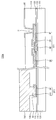
도 2는 도 1에 도시된 표시 장치의 제1 실시예에 따른 단면도이다. FIG. 2 is a cross-sectional view of the first exemplary embodiment of the display device illustrated in FIG. 1.
도 3은 도 1에 도시된 표시 기판의 제2 실시예에 따른 부분 단면도이다. 3 is a partial cross-sectional view of a display substrate of FIG. 1 according to a second exemplary embodiment.
도 4는 도 1에 도시된 표시 기판의 제3 실시예에 따른 부분 단면도이다. 4 is a partial cross-sectional view of a display substrate of FIG. 1 according to a third exemplary embodiment.
도 5는 도 1에 도시된 표시 기판의 제4 실시예에 따른 부분 단면도이다. 5 is a partial cross-sectional view of a display substrate of FIG. 1 according to a fourth exemplary embodiment.
도 6은 도 1에 도시된 표시 기판의 제5 실시예에 따른 부분 단면도이다. 6 is a partial cross-sectional view of a display substrate of FIG. 1 according to a fifth exemplary embodiment.
도 7은 도 1에 도시된 표시 기판의 제6 실시예에 따른 부분 단면도이다. FIG. 7 is a partial cross-sectional view of a display substrate of FIG. 1 according to a sixth exemplary embodiment.
<도면의 주요부분에 대한 부호의 설명><Description of the symbols for the main parts of the drawings>
100a, 100b, 100c, 100d, 100e, 100f : 표시 기판Display substrate: 100a, 100b, 100c, 100d, 100e, 100f
210 : 패드부 220 : 접착부210: pad portion 220: adhesive portion
150 : 도전성 접착층 230 : 게이트 회로부150: conductive adhesive layer 230: gate circuit portion
110 : 게이트 절연층 120 : 보호 절연층110: gate insulating layer 120: protective insulating layer
130 : 유기막 DP1, DP2, DP3 : 더미 패턴130: organic film DP1, DP2, DP3: dummy pattern
SP : 단차보상패턴 400 : 대향 기판SP: Step Compensation Pattern 400: Opposing Substrate
500 : 액정층500: liquid crystal layer
본 발명은 표시 기판 및 이를 구비한 표시 장치에 관한 것으로, 보다 상세하게는 제품의 신뢰성을 향상시키기 위한 표시 기판 및 이를 구비한 표시 장치에 관한 것이다. The present invention relates to a display substrate and a display device having the same, and more particularly, to a display substrate for improving the reliability of a product and a display device having the same.
일반적으로 표시 장치는 표시 패널과 상기 표시 패널을 구동하는 구동회로를 포함한다. 상기 표시 패널은 복수의 게이트 배선들과 복수의 소스 배선들과, 상기 게이트 배선들 및 소스 배선들에 의해 정의되는 복수의 화소부들이 형성된 어레이 기판을 포함한다. 상기 구동회로는 상기 게이트 배선들에 게이트 신호를 제공하는 게이트 구동회로와 상기 소스 배선들에 데이터 신호를 제공하는 소스 구동회로를 포함한다. In general, the display device includes a display panel and a driving circuit for driving the display panel. The display panel includes an array substrate on which a plurality of gate lines, a plurality of source lines, and a plurality of pixel portions defined by the gate lines and source lines are formed. The driving circuit includes a gate driving circuit providing a gate signal to the gate lines and a source driving circuit providing a data signal to the source lines.
상기 게이트 및 소스 구동회로는 칩으로 상기 어레이 기판 상에 실장될 수 있으며, 최근 표시 장치의 슬림화를 위해 상기 게이트 구동회로를 상기 어레이 기판 상에 직접 형성하는 구조가 사용되고 있다. 상기 구조에서는 상기 게이트 구동회로의 부식을 방지하기 위한 방안으로 두꺼운 유기막으로 상기 어레이 기판의 전체 영역을 덮도록 형성한다. The gate and source driving circuits may be mounted on the array substrate by a chip. Recently, a structure for directly forming the gate driving circuit on the array substrate is used to slim the display device. In the structure, a thick organic film is formed to cover the entire region of the array substrate in order to prevent corrosion of the gate driving circuit.
상기 소스 구동회로를 상기 어레이 기판 상에 실장하기 위해 상기 어레이 기판 상에 패드들이 형성된다. 상기 패드들은 상기 유기막에 형성된 콘택홀을 통해 하부 금속층과 전기적으로 연결된다. Pads are formed on the array substrate to mount the source driving circuit on the array substrate. The pads are electrically connected to the lower metal layer through contact holes formed in the organic layer.
상기 어레이 기판을 포함하는 표시 패널은 패널 낙하 검사 공정에서 상기 유기막과 상기 하부 금속층 상의 보호막 간의 약한 결합력에 의해 기판으로부터 보호막이 박리되는 현상이 발생한다. 이때 소스 구동회로가 보호막과 함께 박리된다. 결과적으로 상기 소스 구동회로와 패드들 간의 접촉불량이 발생하여 구동 신뢰성을 저하시키는 문제점이 발생한다. In the display panel including the array substrate, a protective film is peeled from the substrate by a weak bonding force between the organic film and the protective film on the lower metal layer in a panel drop test process. At this time, the source driving circuit is peeled off together with the protective film. As a result, a poor contact between the source driving circuit and the pads occurs, resulting in a problem of lowering driving reliability.
이에 본 발명의 기술적 과제는 이러한 종래의 문제점을 해결하기 위한 것으로, 본 발명의 목적은 신뢰성을 향상시키기 위한 표시 기판을 제공하는 것이다. Accordingly, the technical problem of the present invention is to solve such a conventional problem, and an object of the present invention is to provide a display substrate for improving reliability.
본 발명의 다른 목적은 상기 표시 기판을 구비한 표시 장치를 제공하는 것이다. Another object of the present invention is to provide a display device provided with the display substrate.
상기한 본 발명의 목적을 실현하기 위한 실시예에 따른 표시 기판은 화소 전극, 패드부, 접착부, 더미 패턴 및 도전성 접착부재를 포함한다. 상기 화소 전극은 베이스 기판의 표시 영역에 형성된다. 상기 패드부는 상기 표시 영역을 둘러싸는 주변 영역에 형성된다. 상기 접착부는 상기 패드부와 인접한 영역에 형성된 복수의 홀들을 포함한다. 상기 더미 패턴은 각 홀이 형성된 영역에 형성되어, 상기 홀에 의해 노출된다. 상기 도전성 접착부재는 상기 접착부와 상기 패드부 위에 배치되어, 상기 홀을 통해 상기 더미 패턴과 접착되고 상기 패드부와 집적회로의 단자를 전기적으로 접착한다. The display substrate according to the embodiment for realizing the object of the present invention includes a pixel electrode, a pad portion, an adhesive portion, a dummy pattern and a conductive adhesive member. The pixel electrode is formed in the display area of the base substrate. The pad part is formed in a peripheral area surrounding the display area. The adhesive part includes a plurality of holes formed in an area adjacent to the pad part. The dummy pattern is formed in an area where each hole is formed and is exposed by the hole. The conductive adhesive member is disposed on the adhesive part and the pad part, and adheres to the dummy pattern through the hole, and electrically connects the pad part and the terminal of the integrated circuit.
상기한 본 발명의 다른 목적을 실현하기 위한 실시예에 따른 표시 기판을 구 비한 표시 장치는 표시 패널, 도전성 접착부재 및 집적회로를 포함한다. 상기 표시 패널은 화소 전극이 형성된 표시 영역과 상기 표시 영역을 둘러싸는 주변 영역에 형성된 패드부, 상기 패드부와 인접한 영역에 형성된 복수의 홀들을 포함하는 접착부, 상기 각 홀에 의해 노출되는 더미 패턴을 포함하는 표시 기판과, 상기 표시 기판과 마주하고 상기 표시 영역에 대응하여 컬러 필터층이 형성된 대향 기판을 포함한다. 상기 도전성 접착부재는 상기 패드부와 상기 접착부 위에 형성되고, 상기 홀을 통해 상기 더미 패턴과 접착된다. 상기 집적회로는 상기 도전성 접착부재를 통해 상기 패드부와 전기적으로 접착된다. A display device including a display substrate according to an embodiment for realizing another object of the present invention includes a display panel, a conductive adhesive member, and an integrated circuit. The display panel may include a display area in which a pixel electrode is formed, a pad part formed in a peripheral area surrounding the display area, an adhesive part including a plurality of holes formed in an area adjacent to the pad part, and a dummy pattern exposed by each hole. And a display substrate including an opposing substrate facing the display substrate and having a color filter layer corresponding to the display region. The conductive adhesive member is formed on the pad part and the adhesive part, and is bonded to the dummy pattern through the hole. The integrated circuit is electrically bonded to the pad portion through the conductive adhesive member.
이러한 표시 기판 및 이를 구비한 표시 장치에 의하면, 패드부와 인접한 영역에 형성된 홀들과 상기 각 홀에 의해 노출된 더미 패턴을 형성함으로써 패드부와 상기 패드부에 실장되는 집적회로의 단자와의 접착력을 향상시킬 수 있다. According to the display substrate and the display device having the same, the adhesive force between the pad portion and the terminal of the integrated circuit mounted on the pad portion is formed by forming holes formed in the region adjacent to the pad portion and a dummy pattern exposed by the holes. Can be improved.
도면에서 여러 층 및 영역을 명확하게 표현하기 위하여 두께를 확대하여 나타내었다. 상세한 설명에서 층, 막, 영역, 판 등의 부분이 다른 부분 "위에" 있다고 할 경우, 이는 다른 부분 "바로 위에" 있는 경우뿐만 아니라 그 중간에 또 다른 부분이 있는 경우도 포함한다. 반대로 층, 막, 영역, 판 등의 부분이 다른 부분 "아래에" 있다고 할 경우, 이는 다른 부분 "바로 아래에" 있는 경우뿐만 아니라 그 중간에 또 다른 부분이 있는 경우도 포함한다. In the drawings, the thickness of layers, films, panels, regions, etc., are exaggerated for clarity. In the description, when a part of a layer, film, region, plate, etc. is "on top" of another part, this includes not only being "on" another part but also having another part in between. Conversely, when a part such as a layer, film, region, plate, etc. is "below" another part, this includes not only the other part "below" but also another part in the middle.
이하, 첨부한 도면들을 참조하여, 본 발명을 보다 상세하게 설명하고자 한다.Hereinafter, with reference to the accompanying drawings, it will be described in detail the present invention.
도 1은 본 발명의 실시예에 따른 표시 장치의 평면도이다. 1 is a plan view of a display device according to an exemplary embodiment of the present invention.
도 1을 참조하면, 표시 기판은 표시 영역(DA)과 상기 표시 영역(DA)을 둘러싸는 주변 영역(PA)을 포함한다. 상기 표시 영역(DA)에는 서로 교차하는 방향으로 연장된 복수의 게이트 배선들(GL)과 복수의 소스 배선들(DL)이 형성되고, 상기 게이트 배선들(GL) 및 소스 배선들(DL)에 의해 복수의 화소부들(P)이 정의된다. Referring to FIG. 1, the display substrate includes a display area DA and a peripheral area PA surrounding the display area DA. A plurality of gate lines GL and a plurality of source lines DL may be formed in the display area DA, and may extend in the gate lines GL and the source lines DL. The plurality of pixel portions P is defined.
각 화소부(P)는 해당하는 게이트 배선(GL) 및 소스 배선(DL)에 연결된 스위칭 소자(TFT)와 상기 스위칭 소자(TFT)와 전기적으로 연결된 화소 전극(PE)을 포함한다. Each pixel portion P includes a switching element TFT connected to a corresponding gate line GL and a source line DL, and a pixel electrode PE electrically connected to the switching element TFT.
상기 주변 영역(PA)은 상기 소스 배선들(DL) 단부에 위치하는 제1 회로부(CA1)와 상기 게이트 배선들(GL) 단부에 위치하는 제2 회로부(CA2)를 포함한다. The peripheral area PA includes a first circuit portion CA1 positioned at the end of the source lines DL and a second circuit portion CA2 positioned at the end of the gate lines GL.
상기 제1 회로부(CA1)에는 패드부(210) 및 접착부(220)가 형성된다. 상기 패드부(210)는 복수의 패드들(211)을 포함한다. 구체적으로, 상기 패드부(210)는 실장되는 소스 집적회로(미도시)의 입력단자와 전기적으로 접촉되는 입력패드들(210a)과 출력단자와 전기적으로 접촉되는 출력패드들(210b)을 포함한다. 상기 출력패드부(210b)는 상기 소스 배선들(DL)과 전기적으로 연결되어 상기 소스 배선들(DL)에 데이터 신호를 인가한다. The
상기 접착부(220)는 상기 패드부(210)와 인접한 영역에 형성된 복수의 홀들을 포함한다. 상기 접착부(220)에는 도전성 접착부재가 형성되어, 상기 패드부(210)와 상기 소스 집적회로를 전기적으로 접착시킨다. 상기 접착부(220)는 복수의 홀들에 의해 상기 패드부(210)와 상기 소스 집적회로의 접착력을 강화시키고, 상기 소스 집적회로와 상기 표시 기판 간의 접착력을 강화시킨다. The
상기 제2 회로부(CA2)에는 게이트 회로부(230)가 직접 형성된다. 상기 게이트 회로부(230)는 복수의 스위칭 소자들이 상호 전기적으로 연결된 쉬프트 레지스터를 포함하고, 상기 게이트 배선들(GL)에 게이트 신호를 인가한다. A
도 2는 도 1에 도시된 표시 장치의 제1 실시예에 따른 단면도이다. FIG. 2 is a cross-sectional view of the first exemplary embodiment of the display device illustrated in FIG. 1.
도 1 및 도 2를 참조하면, 표시 장치는 표시 패널과 소스 집적회로(600)를 포함한다. 상기 표시 패널은 표시 기판(100a), 대향 기판(400) 및 액정층(500)을 포함한다. 1 and 2, the display device includes a display panel and a source integrated
상기 표시 기판(100a)은 베이스 기판(101)을 포함한다. 상기 베이스 기판(101) 위에는 제1 금속층으로 제1 금속패턴이 형성된다. 상기 제1 금속패턴은 상기 표시 영역(DA)에 형성되는 게이트 배선들(GL)과 스위칭 소자(TFT)의 게이트 전극(GE)을 포함한다. The
상기 제1 금속패턴이 형성된 베이스 기판(101) 위에 게이트 절연층(110)이 형성되고, 상기 게이트 전극(GE) 위의 상기 게이트 절연층(110)에는 채널층이 형성된다. 상기 채널층은 비정질 실리콘(a-Si)으로 형성된 활성층 및 n+ 이온이 고농도로 도핑된 비정질 실리콘(n+ a_Si)으로 형성된 저항성 접촉층을 포함한다. 상기 채널층을 패터닝하여 상기 게이트 전극(CE) 위에 상기 스위칭 소자(TFT)의 채널부(CH)와 상기 제1 회로부(CA1)에 더미 패턴(DP1)을 형성한다. A
상기 채널부(CH) 및 상기 더미 패턴(DP1)이 형성된 베이스 기판(101) 위에는 제2 금속층으로 형성된 제2 금속패턴이 형성된다. 상기 제2 금속패턴은 상기 표시 영역(DA)에 형성되는 소스 배선들(DL)과 스위칭 소자(TFT)의 소스 및 드레인 전 극(SE, DE)을 포함하고, 상기 제1 회로부(CA1)에 형성된 패드 패턴(211a) 및 상기 제2 회로부(CA2)에 형성된 게이트 회로부(230)의 소스 금속패턴(232)을 포함한다. 상기 소스 금속패턴(232)은 상기 제1 홀(H1)을 통해 상기 게이트 금속패턴(231)과 직접 전기적으로 접촉된다. A second metal pattern formed of a second metal layer is formed on the
상기 제2 금속패턴이 형성된 베이스 기판(101) 위에 보호 절연층(120) 및 유기막(130)을 형성된다. 상기 유기막(130)이 상기 게이트 회로부(230)를 커버함으로써 상기 게이트 회로부(230)의 부식을 방지하여 구동 신뢰성을 향상시킬 수 있다. The protective
상기 보호 절연층(120) 및 유기막(130)에는 상기 드레인 전극(DE)의 일부를 노출시키는 제2 홀(H2)이 형성된다. 상기 표시 영역(DA)에는 상기 제2 홀(H2)을 통해 상기 드레인 전극(DE)과 전기적으로 접촉되는 화소 전극(PE)이 형성된다. A second hole H2 exposing a part of the drain electrode DE is formed in the protective insulating
상기 제1 회로부(CA1)에는 상기 접착부(220)의 제3 홀(H3)과 상기 패드 패턴(211a)을 노출시키는 제4 홀(H3)을 형성한다. 상기 접착부(220)의 제3 홀(H3)은 상기 유기막(130)과 보호 절연층(120)을 패터닝하여 상기 더미 패턴(DP1)을 노출시킨다. A fourth hole H3 exposing the third hole H3 of the
상기 더미 패턴(DP1)이 형성되지 않은 경우, 상기 접착부(220)의 제3 홀(H3)을 형성하기 위해 상기 보호 절연층(120)을 에칭하는 공정 중 오버 에칭에 의해 상기 게이트 절연층(110)이 식각된다. 상기 오버 에칭에 의해 상기 게이트 절연층(110)은 대략 700Å 정도 제거된다. 따라서, 상기 보호 절연층(120) 에칭시 상기 게이트 절연층(110)이 오버 에칭되는 것을 막기 위해 상기 제3 홀(H3)이 형성되는 영역에 대응하여 상기 채널층으로 형성된 더미 패턴(DP1)을 형성한다. 상기 더미 패턴(DP1)의 두께는 상기 오버 에칭되는 두께 보다 두꺼운 대략 700Å ~ 1500Å 정도가 바람직하다. When the dummy pattern DP1 is not formed, the
상기 더미 패턴(DP1)에 의해 상기 보호 절연층(120) 에칭시 상기 게이트 절연층(110)이 식각되지 않음에 따라서 상기 도전성 접착부재(150)는 상기 제3 홀(H3)의 바닥면인 상기 더미 패턴(DP1)과 접촉되고, 상기 제3 홀(H3)의 측면인 상기 보호 절연층(120) 및 유기막(130)과 순차적으로 접착된다. 따라서 상기 표시 기판(100a)과 상기 도전성 접착부재(150) 간의 접착력을 강화시킨다. 결과적으로 상기 제1 회로부(CA1)에 실장된 상기 소스 집적회로와 상기 패드부(210)의 접착력을 강화시켜 구동 신뢰성을 향상시킬 수 있다. As the
상기 제4 홀(H4)을 통해 상기 패드 패턴(211a)과 전기적으로 접촉되는 패드 전극(211b)이 형성된다. 상기 제1 회로부(CA1)에는 상기 패드 패턴(211a)과 패드 전극(211b)을 포함하는 패드(211)가 형성된다. 바람직하게 상기 제1 회로부(CA1)의 유기막(130)은 상기 표시 영역(DA)에 형성된 유기막(130)의 두께 보다 얇게 형성하여 상기 제3 및 제4 홀(H3, H4)의 단차를 최소화한다. A
상기 대향 기판(400)은 차광층(410), 컬러 필터층(420) 및 공통 전극층(440)을 포함한다. The opposing
상기 차광층(410)은 광을 차단하는 물질로 형성된다. 바람직하게 상기 차광층(410)은 상기 표시 영역(DA)의 소스 배선(DL) 및 게이트 배선(GL)에 대응하는 영역에 형성되어 누설 광을 차단하고, 상기 표시 영역(DA)과 인접한 주변 영역(PA)에 형성되어 상기 표시 영역(DA)의 시인성을 향상시킨다. The
상기 컬러 필터층(420)은 상기 차광층(410)에 의해 정의된 상기 표시 영역(DA)의 화소 영역에 형성되어, 투과되는 광을 컬러 광으로 필터링한다. 상기 공통 전극층(440)은 상기 표시 기판(100a)의 화소 전극(PE)에 대향하는 전극으로 상기 액정층(500a)에 전계를 형성한다. The
상기 소스 집적회로(600)는 구동 칩 및 구동 칩이 실장된 연성회로기판(Flexible Printed Circuit : FPC)을 포함한다. 상기 소스 집적회로(600)는 복수의 단자(610)들을 포함한다. The source
상기 소스 집적회로(600)는 상기 표시 기판(100a)의 제1 회로부(CA1)에 실장된다. 상기 제1 회로부(CA1)에 형성된 도전성 접착부재(150)는 상기 단자(610)와 상기 패드(211)를 전기적으로 연결한다. 상기 도전성 접착부재(150)는 상기 제3 홀(H3)들을 통해 상기 더미 패턴(DP1)과 접착되어 상기 소스 집적회로(600)와 상기 패드부(210)의 접착력을 강화시킨다. The source
즉, 상기 접착부(220)와 상기 도전성 접착부재(150) 간의 접착력에 의해 외부 충격으로부터 상기 보호 절연층(120)과 유기막(130)이 박리되는 것을 막아 상기 소스 집적회로(600)와 패드부(210) 간의 전기적 접촉 불량을 방지할 수 있다. That is, the source
도 3은 도 1에 도시된 표시 기판의 제2 실시예에 따른 부분 단면도이다. 3 is a partial cross-sectional view of a display substrate of FIG. 1 according to a second exemplary embodiment.
도 2 및 도 3을 참조하면, 상기 표시 기판(100b)은 상기 도 2의 표시 기판(100a)에 상기 더미 패턴(DP1)의 아래에 형성된 단차보상패턴(SP)을 더 포함한다. 상기 단차보상패턴(SP)은 상기 제1 금속층으로 형성된 것으로, 상기 제1 금속패턴에 포함된다. 상기 단차보상패턴(SP)은 상기 제3 홀(H3)에 형성된 상기 유기 막(130)의 단차를 줄일 수 있다. 2 and 3, the
상기 단차보상패턴(SP)에 의해 단차가 보상됨에 따라 상기 제3 홀(H3)을 통해 상기 더미 패턴(DP1)과 접착되는 상기 도전성 접착부재(150)의 접착력을 강화시킬 수 있다.As the step is compensated by the step compensation pattern SP, the adhesive force of the conductive
도 4는 도 1에 도시된 표시 기판의 제3 실시예에 따른 부분 단면도이다. 4 is a partial cross-sectional view of a display substrate of FIG. 1 according to a third exemplary embodiment.
도 1 및 도 4를 참조하면, 표시 기판(100c)의 제1 회로부(CA1)에는 제3 홀(H3)을 포함하는 접착부(220)가 형성된다. 상기 접착부(220)의 제3 홀(H3)은 더미 패턴(DP2)을 노출시키도록 상기 보호 절연층(120) 및 유기막(130)이 패터닝되어 형성된다. 상기 더미 패턴(DP2)은 상기 제2 금속층으로 형성된 것으로, 상기 제2 금속패턴에 포함된다. 1 and 4, an
따라서 상기 도전성 접착부재(150)는 상기 접착부(220)의 제3 홀(H3)을 통해 상기 더미 패턴(DP2), 상기 보호 절연층(120) 및 유기막(130)과 순차적으로 접착되어 상기 베이스 기판(101)과의 접착력이 강화된다. 일반적으로 금속물질과 유기물간의 접착력이 우수한 특성에 따라 상기 제2 금속층으로 형성된 상기 더미 패턴(DP2)과 상기 도전성 접착부재(150) 간의 접착력이 우수하다. 이에 따라서 접착력이 약한 상기 유기막(130)과 보호 절연층(120) 간의 접착력을 강화시킬 수 있다.Accordingly, the conductive
결과적으로 상기 제1 회로부(CA1)에 실장된 상기 소스 집적회로와 상기 패드부(210)의 접착력을 강화시켜 구동 신뢰성을 향상시킬 수 있다. As a result, driving reliability may be improved by strengthening the adhesion between the source integrated circuit mounted on the first circuit part CA1 and the
도 5는 도 1에 도시된 표시 기판의 제4 실시예에 따른 부분 단면도이다. 5 is a partial cross-sectional view of a display substrate of FIG. 1 according to a fourth exemplary embodiment.
도 4 및 도 5를 참조하면, 상기 표시 기판(100d)은 상기 도 3의 표시 기 판(100c)에 상기 더미 패턴(DP2)의 아래에 형성된 단차보상패턴(SP)을 더 포함한다. 4 and 5, the
상기 단차보상패턴(SP)은 상기 제1 금속층으로 형성된 상기 제1 금속패턴에 포함된다. 상기 단차보상패턴(SP)은 상기 제3 홀(H3)에 형성된 상기 유기막(130)의 단차를 줄여준다. 상기 단차보상패턴(SP)에 의해 단차가 보상됨에 따라 상기 제3 홀(H3)을 통해 상기 더미 패턴(DP2)과 접착되는 상기 도전성 접착부재(150)의 접착력을 더욱 강화시킬 수 있다.The step compensation pattern SP is included in the first metal pattern formed of the first metal layer. The step compensation pattern SP reduces the step difference of the
도 6은 도 1에 도시된 표시 기판의 제5 실시예에 따른 부분 단면도이다. 6 is a partial cross-sectional view of a display substrate of FIG. 1 according to a fifth exemplary embodiment.
도 1 및 도 6을 참조하면, 표시 기판(100e)의 제1 회로부(CA1)에는 제3 홀(H3)을 포함하는 접착부(220)가 형성된다. 상기 접착부(220)의 제3 홀(H3)은 더미 패턴(DP3)을 노출시키도록 상기 보호 절연층(120) 및 유기막(130)이 패터닝되어 형성된다. 상기 더미 패턴(DP3)은 상기 채널층으로 형성된 제1 더미 패턴(DP1)과 상기 제2 금속층으로 형성된 제2 더미 패턴(DP2)이 적층된 구조를 갖는다. 상기 더미 패턴(DP3)은 상기 채널층과 상기 제2 금속층을 하나의 마스크를 이용하여 동시에 패터닝하여 형성된다. 1 and 6, an
따라서 상기 도전성 접착부재(150)는 상기 제3 홀(H3)의 바닥면인 상기 더미 패턴(DP3)의 제2 더미 패턴(DP2)과 접착되고, 상기 제3 홀(H3)의 측면인 상기 보호 절연층(120) 및 유기막(130)과 순차적으로 접착된다. 일반적으로 금속물질과 유기물간의 접착력이 우수한 특성에 따라 상기 제2 금속층으로 형성된 상기 제2 더미 패턴(DP2)과 상기 도전성 접착부재(150) 간의 접착력이 우수하다. 이에 따라 접착 력이 약한 상기 유기막(130)과 보호 절연층(120) 간의 접착력을 강화시킨다. Therefore, the conductive
결과적으로 상기 제1 회로부(CA1)에 실장된 상기 소스 집적회로와 상기 패드부(210)의 접착력을 강화시켜 구동 신뢰성을 향상시킬 수 있다. As a result, driving reliability may be improved by strengthening the adhesion between the source integrated circuit mounted on the first circuit part CA1 and the
한편, 상기 표시 기판(100e)의 표시 영역에 형성된 소스 배선(DL)과, 스위칭 소자(TFT)의 소스 및 드레인 전극(SE, DE) 역시 상기 채널층과 상기 제2 금속층을 하나의 마스크를 이용하여 패터닝되어 형성된다. 따라서 상기 소스 배선(DL), 상기 소스 전극(SE) 및 드레인 전극(DE)은 상기 채널층 및 상기 제2 금속층이 적층된 구조로 형성된다. On the other hand, the source wiring DL formed in the display area of the
도 7은 도 1에 도시된 표시 기판의 제6 실시예에 따른 부분 단면도이다. FIG. 7 is a partial cross-sectional view of a display substrate of FIG. 1 according to a sixth exemplary embodiment.
도 6 및 도 7을 참조하면, 상기 표시 기판(100f)은 상기 도 6의 표시 기판(100e)에 상기 더미 패턴(DP3)의 아래에 형성된 단차보상패턴(SP)을 더 포함한다. 상기 단차보상패턴(SP)은 상기 제1 금속층으로 형성된 상기 제1 금속패턴에 포함된다. 상기 단차보상패턴(SP)은 상기 제3 홀(H3)에 형성된 상기 유기막(130)의 단차를 줄여준다. 상기 단차보상패턴(SP)에 의해 단차가 보상됨에 따라 상기 제3 홀(H3)을 통해 상기 더미 패턴(DP3)과 접착되는 상기 도전성 접착부재(150)의 접착력을 더욱 강화시킬 수 있다. 6 and 7, the
이상에서 설명한 바와 같이, 본 발명에 따르면 패드부와 인접한 영역에 복수의 홀들을 포함하는 접착부를 형성함으로써, 상기 패드부와 도전성 접착부재를 통해 전기적으로 연결되는 집적회로와 접착력을 향상시킬 수 있다. As described above, according to the present invention, by forming an adhesive part including a plurality of holes in an area adjacent to the pad part, the integrated circuit and the adhesive force electrically connected through the pad part and the conductive adhesive member can be improved.
또한, 상기 접착부의 홀들을 통해 더미 패턴을 노출시켜 상기 도전성 접착부재와 상기 더미 패턴을 접착시킴으로써 표시 기판과 상기 도전성 접착부재의 접착력을 강화시킬 수 있다. In addition, the adhesive pattern between the display substrate and the conductive adhesive member may be strengthened by exposing the dummy pattern through the holes of the adhesive part to bond the conductive adhesive member to the dummy pattern.
구체적으로 상기 더미 패턴이 채널층으로 형성되는 경우는 보호 절연층 에칭 공정시 게이트 절연층이 오버 에칭되는 것을 방지하여 표시 기판의 하부 절연층 예컨대, 게이트 절연층 또는 보호 절연층과 상기 도전성 접착부재가 접촉됨으로써 접착력이 약한 유기막과 보호 절연층 간의 접착력을 강화시킬 수 있다. 또한, 상기 더미 패턴이 금속층으로 형성되는 경우 상기 더미 패턴과 상기 도전성 접착부재의 접착력을 강화시켜 접착력이 약한 유기막과 보호 절연층 간의 접착력을 강화시킬 수 있다. 이에 따라서 상기 유기막과 보호 절연층 간의 박리 현상에 의해 상기 집적회로와 패드부 간의 접촉 불량을 막을 수 있다. Specifically, when the dummy pattern is formed as a channel layer, the gate insulating layer is prevented from being overetched during the protective insulating layer etching process, so that the lower insulating layer, for example, the gate insulating layer or the protective insulating layer, and the conductive adhesive member of the display substrate are prevented. By contacting, the adhesive force between the organic film and the protective insulating layer which are weak in adhesive force can be strengthened. In addition, when the dummy pattern is formed of a metal layer, the adhesive force between the dummy pattern and the conductive adhesive member may be strengthened to enhance the adhesive force between the organic layer having a weak adhesive force and the protective insulating layer. Accordingly, poor contact between the integrated circuit and the pad part can be prevented by the peeling phenomenon between the organic layer and the protective insulating layer.
이상에서는 실시예를 참조하여 설명하였지만, 해당 기술 분야의 숙련된 당업자는 하기의 특허 청구의 범위에 기재된 본 발명의 사상 및 영역으로부터 벗어나지 않는 범위 내에서 본 발명을 다양하게 수정 및 변경시킬 수 있음을 이해할 수 있을 것이다.Although described above with reference to the embodiments, those skilled in the art can be variously modified and changed within the scope of the invention without departing from the spirit and scope of the invention described in the claims below. I can understand.
Claims (18)
Priority Applications (4)
| Application Number | Priority Date | Filing Date | Title |
|---|---|---|---|
| KR1020070043674A KR20080098242A (en) | 2007-05-04 | 2007-05-04 | Display substrate and display device having same |
| JP2008040140A JP5525692B2 (en) | 2007-02-22 | 2008-02-21 | Display substrate, manufacturing method thereof, and display device including the same |
| CN2008101428980A CN101320148B (en) | 2007-02-22 | 2008-02-22 | Display substrate, method of manufacturing the same and display device having the display substrate |
| US12/035,556 US7796228B2 (en) | 2007-02-22 | 2008-02-22 | Display substrate, method of manufacturing the same and display device having the same |
Applications Claiming Priority (1)
| Application Number | Priority Date | Filing Date | Title |
|---|---|---|---|
| KR1020070043674A KR20080098242A (en) | 2007-05-04 | 2007-05-04 | Display substrate and display device having same |
Publications (1)
| Publication Number | Publication Date |
|---|---|
| KR20080098242A true KR20080098242A (en) | 2008-11-07 |
Family
ID=40285810
Family Applications (1)
| Application Number | Title | Priority Date | Filing Date |
|---|---|---|---|
| KR1020070043674A Withdrawn KR20080098242A (en) | 2007-02-22 | 2007-05-04 | Display substrate and display device having same |
Country Status (1)
| Country | Link |
|---|---|
| KR (1) | KR20080098242A (en) |
Cited By (2)
| Publication number | Priority date | Publication date | Assignee | Title |
|---|---|---|---|---|
| CN107919067A (en) * | 2016-10-06 | 2018-04-17 | 三星显示有限公司 | Flat-panel monitor |
| US20220317508A1 (en) * | 2020-10-23 | 2022-10-06 | Fuzhou Boe Optoelectronics Technology Co., Ltd. | Display substrate and method for manufacturing the same, display device |
-
2007
- 2007-05-04 KR KR1020070043674A patent/KR20080098242A/en not_active Withdrawn
Cited By (3)
| Publication number | Priority date | Publication date | Assignee | Title |
|---|---|---|---|---|
| CN107919067A (en) * | 2016-10-06 | 2018-04-17 | 三星显示有限公司 | Flat-panel monitor |
| US20220317508A1 (en) * | 2020-10-23 | 2022-10-06 | Fuzhou Boe Optoelectronics Technology Co., Ltd. | Display substrate and method for manufacturing the same, display device |
| US12222596B2 (en) * | 2020-10-23 | 2025-02-11 | Fuzhou Boe Optoelectronics Technology Co., Ltd. | Display substrate with a bonding pad including conductive parts in different layers and method for manufacturing the same, display device |
Similar Documents
| Publication | Publication Date | Title |
|---|---|---|
| JP5525692B2 (en) | Display substrate, manufacturing method thereof, and display device including the same | |
| US7170570B2 (en) | Liquid crystal display | |
| KR100763408B1 (en) | Liquid crystal display | |
| KR101119196B1 (en) | Display apparatus and method of fabricating the same | |
| KR100685945B1 (en) | LCD and its manufacturing method | |
| KR101365118B1 (en) | Display substrate, method of manufacturing the same and display device having the display substrate | |
| US8111367B2 (en) | Display device | |
| KR101119184B1 (en) | Array substrate, display apparatus having the same and method of manufacturing the same | |
| KR20080102730A (en) | Display | |
| KR20080098242A (en) | Display substrate and display device having same | |
| KR100635944B1 (en) | Thin film transistor substrate for liquid crystal display | |
| KR100339334B1 (en) | the Structure of the LCD Pad and the Method for fabricating it | |
| KR100816335B1 (en) | Thin film transistor substrate and method for attaching driving integrated circuit using same | |
| KR100200435B1 (en) | Liquid crystal display device | |
| TWI283787B (en) | Liquid crystal display | |
| KR101035915B1 (en) | Liquid crystal display | |
| KR20130062819A (en) | Liquid crystal display device | |
| KR20080008703A (en) | Array substrate, display panel having same and manufacturing method thereof | |
| KR20060087712A (en) | LCD Display | |
| KR101216175B1 (en) | Liquid crystal display | |
| KR20050066710A (en) | Liquid crystal display device | |
| KR101168886B1 (en) | Liquid crystal displau divece for preventing delay of common signal | |
| KR20080020852A (en) | Printed circuit board and printed circuit board assembly including the same | |
| KR20040098869A (en) | Pad structure of liquid crystal display |
Legal Events
| Date | Code | Title | Description |
|---|---|---|---|
| PA0109 | Patent application |
Patent event code: PA01091R01D Comment text: Patent Application Patent event date: 20070504 |
|
| PG1501 | Laying open of application | ||
| PC1203 | Withdrawal of no request for examination | ||
| WITN | Application deemed withdrawn, e.g. because no request for examination was filed or no examination fee was paid |