KR20080034858A - Electrical connecting element - Google Patents
Electrical connecting element Download PDFInfo
- Publication number
- KR20080034858A KR20080034858A KR1020077030995A KR20077030995A KR20080034858A KR 20080034858 A KR20080034858 A KR 20080034858A KR 1020077030995 A KR1020077030995 A KR 1020077030995A KR 20077030995 A KR20077030995 A KR 20077030995A KR 20080034858 A KR20080034858 A KR 20080034858A
- Authority
- KR
- South Korea
- Prior art keywords
- electrical
- coating
- electrical conductor
- connection element
- rough surface
- Prior art date
Links
Images


Classifications
-
- H—ELECTRICITY
- H01—ELECTRIC ELEMENTS
- H01R—ELECTRICALLY-CONDUCTIVE CONNECTIONS; STRUCTURAL ASSOCIATIONS OF A PLURALITY OF MUTUALLY-INSULATED ELECTRICAL CONNECTING ELEMENTS; COUPLING DEVICES; CURRENT COLLECTORS
- H01R13/00—Details of coupling devices of the kinds covered by groups H01R12/70 or H01R24/00 - H01R33/00
- H01R13/02—Contact members
- H01R13/03—Contact members characterised by the material, e.g. plating, or coating materials
-
- H—ELECTRICITY
- H01—ELECTRIC ELEMENTS
- H01R—ELECTRICALLY-CONDUCTIVE CONNECTIONS; STRUCTURAL ASSOCIATIONS OF A PLURALITY OF MUTUALLY-INSULATED ELECTRICAL CONNECTING ELEMENTS; COUPLING DEVICES; CURRENT COLLECTORS
- H01R12/00—Structural associations of a plurality of mutually-insulated electrical connecting elements, specially adapted for printed circuits, e.g. printed circuit boards [PCB], flat or ribbon cables, or like generally planar structures, e.g. terminal strips, terminal blocks; Coupling devices specially adapted for printed circuits, flat or ribbon cables, or like generally planar structures; Terminals specially adapted for contact with, or insertion into, printed circuits, flat or ribbon cables, or like generally planar structures
- H01R12/50—Fixed connections
- H01R12/59—Fixed connections for flexible printed circuits, flat or ribbon cables or like structures
- H01R12/61—Fixed connections for flexible printed circuits, flat or ribbon cables or like structures connecting to flexible printed circuits, flat or ribbon cables or like structures
-
- H—ELECTRICITY
- H01—ELECTRIC ELEMENTS
- H01R—ELECTRICALLY-CONDUCTIVE CONNECTIONS; STRUCTURAL ASSOCIATIONS OF A PLURALITY OF MUTUALLY-INSULATED ELECTRICAL CONNECTING ELEMENTS; COUPLING DEVICES; CURRENT COLLECTORS
- H01R4/00—Electrically-conductive connections between two or more conductive members in direct contact, i.e. touching one another; Means for effecting or maintaining such contact; Electrically-conductive connections having two or more spaced connecting locations for conductors and using contact members penetrating insulation
- H01R4/02—Soldered or welded connections
- H01R4/021—Soldered or welded connections between two or more cables or wires
-
- H—ELECTRICITY
- H01—ELECTRIC ELEMENTS
- H01R—ELECTRICALLY-CONDUCTIVE CONNECTIONS; STRUCTURAL ASSOCIATIONS OF A PLURALITY OF MUTUALLY-INSULATED ELECTRICAL CONNECTING ELEMENTS; COUPLING DEVICES; CURRENT COLLECTORS
- H01R4/00—Electrically-conductive connections between two or more conductive members in direct contact, i.e. touching one another; Means for effecting or maintaining such contact; Electrically-conductive connections having two or more spaced connecting locations for conductors and using contact members penetrating insulation
- H01R4/04—Electrically-conductive connections between two or more conductive members in direct contact, i.e. touching one another; Means for effecting or maintaining such contact; Electrically-conductive connections having two or more spaced connecting locations for conductors and using contact members penetrating insulation using electrically conductive adhesives
-
- H—ELECTRICITY
- H01—ELECTRIC ELEMENTS
- H01R—ELECTRICALLY-CONDUCTIVE CONNECTIONS; STRUCTURAL ASSOCIATIONS OF A PLURALITY OF MUTUALLY-INSULATED ELECTRICAL CONNECTING ELEMENTS; COUPLING DEVICES; CURRENT COLLECTORS
- H01R43/00—Apparatus or processes specially adapted for manufacturing, assembling, maintaining, or repairing of line connectors or current collectors or for joining electric conductors
- H01R43/02—Apparatus or processes specially adapted for manufacturing, assembling, maintaining, or repairing of line connectors or current collectors or for joining electric conductors for soldered or welded connections
Landscapes
- Connections Effected By Soldering, Adhesion, Or Permanent Deformation (AREA)
- Photovoltaic Devices (AREA)
Abstract
Description
본 발명은 전기 전도체 및 전기 전도성 코팅을 포함하는 전기적 연결 소자에 관한 것이다. The present invention relates to an electrical connection element comprising an electrical conductor and an electrically conductive coating.
플랫 (flat) 와이어로서 설계되며 땜납 코팅을 가지는 전기적 연결 소자는 이미 공지되어 있다.Electrically connected elements designed as flat wire and having a solder coating are already known.
상기 공지된 연결 소자는 몇 개의 전기 요소, 예컨대 전기 요소, 예컨대 솔라 셀 (solar cell) 을 서로 전기적으로 연결시키는데 사용된다. 이를 위하여, 상기 연결 소자는 가열되어, 코팅의 용융에 의해 상기 전기 요소와 납땜된다. 또한, 펀치가공된 부품 또는 컷 밴드로서 설계된 코팅된 연결 소자 또한 공지되어 있다.The known connection elements are used to electrically connect several electrical elements, such as electrical elements, such as solar cells. For this purpose, the connecting element is heated and soldered with the electrical element by melting of the coating. Coated connection elements designed as punched parts or cut bands are also known.
상기 공지된 연결 소자는, 코팅을 가능한 한 빨리 가열하기 위해서 상당한 에너지 량이 요구된다는 단점을 가진다. 그렇지 않으면, 상기 코팅은 충분하고도 빨리 가열될 수 없어, 전기 전도체와 전기 요소간의 안정적인 연결이 얻어질 수 없게 된다.The known connection elements have the disadvantage that a significant amount of energy is required to heat the coating as soon as possible. Otherwise, the coating cannot be heated sufficiently and quickly so that a stable connection between the electrical conductor and the electrical element cannot be obtained.
따라서, 본 발명의 목적은 앞서 언급된 종류의 연결 소자를 제공하는데 있으며, 상기 연결 소자는 쉽게 기계가공 가능하고, 전기 전도체와 전기 요소간의 안정적인 연결이 높은 공정 속도로 이루어지도록 신속히 가열될 수 있는 코팅을 가진다.It is therefore an object of the present invention to provide a connection element of the kind mentioned above, the connection element being easily machined and a coating which can be quickly heated to ensure a stable connection between the electrical conductor and the electrical element at a high process speed. Has
본 발명에 따르면, 이러한 목적은 적어도 일부 영역에서의 전기 전도체의 표면에 구조체 및/또는 거친 면을 제공하는 것으로 달성된다.According to the invention, this object is achieved by providing a structure and / or a rough surface on the surface of the electrical conductor in at least some areas.
이는, 코팅의 확대된 유효 표면이 처리되지 않은 표면과 비교해 볼 때 활용가능하다는 점과 상기 코팅의 확대된 유효 표면은 높은 광학적 및/또는 열적 흡수성을 가진다는 이점을 제공한다. 땜납 또는 접합 공정과 관련해 볼 때, 요구되는 열은 쉽고 빠르게 도입될 수 있다. 상기 코팅은 표면 처리에 의해 구조체 및/또는 거친 면이 형성되는 균일한 재료로 만들어지는 것이 바람직하다. 상기 균일성은 전체 층을 균일하게 가열할 수 있어, 일련의 접합 공정에 활용가능하게 된다.This provides the advantage that the enlarged effective surface of the coating is available in comparison to the untreated surface and that the enlarged effective surface of the coating has high optical and / or thermal absorption. With regard to the soldering or joining process, the required heat can be introduced easily and quickly. The coating is preferably made of a uniform material on which the structures and / or rough surfaces are formed by surface treatment. The uniformity allows the entire layer to be heated evenly, making it available for a series of joining processes.
본 발명의 실시형태에 따르면, 전기 전도성 코팅은 땜납가능한 재료 예컨대, 땜납, 특히 주석을 함유할 수 있다. 이로써, 상기 코팅 자체는 일 가공 단계로 단단히 부착된 땜납 처리된 연결부가 이루어질 수 있다.According to an embodiment of the invention, the electrically conductive coating may contain a solderable material such as solder, in particular tin. In this way, the coating itself can be made with soldered connections firmly attached in one processing step.
다른 실시형태에 따르면, 전기 전도성 코팅은 접착제, 바람직하게는 전도성 접착제를 포함할 수 있다. 이로써, 상기 코팅은 단단히 부착된 접착성 접합부를 형성할 수 있다.According to another embodiment, the electrically conductive coating may comprise an adhesive, preferably a conductive adhesive. As such, the coating may form a tightly attached adhesive bond.
상기 전기 전도체는 금속, 특히 구리, 또는 금속 합금, 특히 구리 합금으로 만들어지는 것이 유리하다. 이로써, 가공 용이성뿐만 아니라 특별히 높은 전기 전도성이 얻어진다.The electrical conductor is advantageously made of a metal, in particular copper, or a metal alloy, in particular a copper alloy. This results in not only easy processing but also particularly high electrical conductivity.
본 발명의 다른 개선안에 있어서, 구조체 및/또는 거친 면은 널링 가공부 또는 플로팅 (floating) 가공부로 이루어질 수 있다. 상기 표면 변경은 예컨대, 롤링에 의해 특히 쉽고 자동적으로 이루어질 수 있다. In another refinement of the invention, the structure and / or rough surface may consist of a knurled or floating workpiece. The surface change can be made particularly easily and automatically, for example by rolling.
다른 실시형태에 있어서, 상기 구조체 및/또는 거친 면은 그라인딩을 통하여 형성될 수 있다. 이로써, 기계가공 방향과 무관하고 표면 상의 모든 방향에서 동일한 특성을 지닌 코팅을 제공할 수 있다.In other embodiments, the structure and / or rough surface may be formed through grinding. This makes it possible to provide coatings that are independent of the machining direction and have the same properties in all directions on the surface.
다른 실시형태에 따르면, 구조체 및/또는 거친 면은 에칭을 통하여 형성될 수 있다. 마찬가지로, 균일한 표면 변경은 이러한 화학적 처리에 의해 얻어질 수 있다.According to another embodiment, the structure and / or rough surface may be formed through etching. Likewise, a uniform surface change can be obtained by this chemical treatment.
다른 개선안에 있어서, 구조체 및/또는 거친 면은, 에너지 흡수를 목적으로 한 코팅의 영역에만 걸친 단면에 뻗어 있을 수 있다. 이로써, 코팅의 전체 표면을 처리할 필요가 없다. 그래서, 연결 소자를 전기 요소 상에 연결 적용시키는 관점에 있어서, 예컨대, 적외선 광으로 후에 방출되는 표면 영역만이 변경되어져야 한다.In another refinement, the structure and / or rough side may extend in a cross section over only the area of the coating for the purpose of energy absorption. This eliminates the need to treat the entire surface of the coating. Thus, from the point of view of connecting the connecting element onto the electrical element, for example, only the surface area which is later emitted with infrared light has to be changed.
다른 변형예에 따르면, 상기 구조체 및/또는 거친 면은 전기 전도체의 전체 외주에 걸친 단면에 뻗어있을 수 있다. 이러한 설계로, 본 발명에 따른 연결 소자를 이용할 때에는 변경된 표면이 제공된 코팅의 일부에 주의를 기울일 필요가 없다. 따라서, 가공 단계는 간소화된다. According to another variant, the structure and / or rough surface may extend in cross section over the entire perimeter of the electrical conductor. With this design, it is not necessary to pay attention to the part of the coating provided with the altered surface when using the connecting element according to the invention. Thus, the machining step is simplified.
상기 전기 전도체는 펀치 가공된 부품 또는 컷 밴드로 만들어지는 것이 유리하다. 그래서, 상기 연결 소자는 특히 생산이 용이하며 가격이 절감된다.The electrical conductor is advantageously made of a punched part or cut band. Thus, the connecting element is particularly easy to produce and the cost is reduced.
바람직한 실시형태에서, 상기 전기 전도체는 단면에 비하여 큰 길이 치수를 가질 수 있으며, 예컨대, 와이어로서 설계될 수 있다. 이로써, 일 가공 단계로 연결 소자를 통하여 서로 몇 개의 전기 요소를 연결할 수 있다. In a preferred embodiment, the electrical conductor can have a large length dimension relative to the cross section, for example designed as a wire. In this way, several electrical elements can be connected to one another via a connecting element in one machining step.
널링 또는 플로팅 가공부는 본질적으로 전기 전도체의 길이방향 연장부와 평행하게 뻗어있는 것이 유리하다. 이는, 상기 플로팅 또는 널링 가공부가 연결 소자의 생산 동안에 연속적인 가공에 쉽게 적용될 수 있다는 이점을 가진다. 또한, 길이방향 연장부에 걸쳐 균일한 표면 및 이에 따른 코팅의 균일한 특성이 특히 유리한 방식으로 얻어진다.It is advantageous for the knurled or floating workpiece to extend essentially parallel to the longitudinal extension of the electrical conductor. This has the advantage that the floating or nulling processing part can be easily applied to continuous processing during the production of the connecting element. In addition, a uniform surface and thus uniform properties of the coating over the longitudinal extension are obtained in a particularly advantageous manner.
다른 변형 예에서, 그라인딩 방향은 본질적으로 전기 전도체의 길이방향 연장부와 평행하게 뻗어있을 수 있다. 또한, 이러한 경우에, 표면 처리는 연속적인 공정으로 쉽게 실행될 수 있다. 마찬가지로, 길이방향 연장부에 걸쳐 균일한 표면 및 이에 따른 코팅의 균일한 특성이 특히 유리한 방식으로 얻어진다.In other variations, the grinding direction may extend essentially parallel to the longitudinal extension of the electrical conductor. Also in this case, the surface treatment can be easily carried out in a continuous process. Likewise, a uniform surface and thus uniform properties of the coating over the longitudinal extension are obtained in a particularly advantageous manner.
다른 실시형태에서, 전기 전도체는 원형 단면일 수 있다. 때문에, 시중에서 구입가능한 와이어를 사용할 수 있다.In other embodiments, the electrical conductor may be of circular cross section. Therefore, a commercially available wire can be used.
특히 바람직한 실시형태에서, 전기 전도체는, 원형 형태에서 벗어난 형상, 예컨대 사각형, 특히 편평한 와이어로 설계된 형상으로 이루어진 단면으로 설계될 수 있다. 이러한 설계로 인하여, 전기 요소에 대한 연결 소자의 특히 우수한 부착이 큰 접촉면의 도움으로 얻어질 수 있다. 또한, 코팅의 활용가능한 표면은 확장되며, 이는 보다 용이한 열 진입을 가능케 한다.In a particularly preferred embodiment, the electrical conductor can be designed in a cross section consisting of a shape out of circular shape, for example a shape designed with a square, in particular flat wire. Due to this design, particularly good attachment of the connecting element to the electrical element can be obtained with the aid of a large contact surface. In addition, the usable surface of the coating is expanded, which allows for easier heat entry.
다른 실시형태에 있어서, 코팅의 표면에는, 연결 소자의 전체 길이에 걸쳐 구조체 및/또는 거친 면이 제공될 수 있다. 이로써, 특히 간단한 생산 및 가공뿐만 아니라 특히 높은 열 진입이 가능하다. 상기 구조체 및/또는 거친 면은 생산 동안에 일련의 가공으로 형성될 수 있으며, 코팅의 동일 특성은 상기 가공 동안에 각각의 장소에서 얻어진다.In another embodiment, the surface of the coating may be provided with a structure and / or rough surface over the entire length of the connecting element. This allows particularly high heat entry as well as particularly simple production and processing. The structure and / or rough side can be formed in a series of processes during production, and the same properties of the coating are obtained at each site during the process.
상기 코팅은 연결 소자의 전체 길이에 걸쳐 뻗어있는 것이 유리한다. 여기서, 상기 가공 동안에는 코팅이 위치되는 위치 및 전기 전도체에 대한 표면 보호가 상기 코팅을 통하여 얻어질 수 있는 위치에 주의를 기울일 필요가 없다는 이점이 있다.The coating advantageously extends over the entire length of the connecting element. Here, there is an advantage that during the processing there is no need to pay attention to where the coating is located and where the surface protection for the electrical conductor can be obtained through the coating.
바람직한 용도에 있어서, 본 발명에 따른 연결 소자는 솔라셀에 적용될 수 있다. 솔라셀과 전기 전도체 간의 연결의 안정적인 실행은 이러한 용도에 특히 중요하며, 따라서, 본 발명에 따른 코팅 상에 구조체 및/또는 거친 면을 적용하는 것은 특히 유리하다.In a preferred use, the connection element according to the invention can be applied to solar cells. The stable implementation of the connection between the solar cell and the electrical conductor is of particular importance for this application and it is therefore particularly advantageous to apply the structure and / or rough side on the coating according to the invention.
다른 실시형태에서, 두 개 이상의 솔라셀은 본 발명에 다른 연결 소자를 통하여 서로 연결될 수 있다. 결과적으로, 몇 개의 솔라셀은 연결 소자와 연결될 수 있어, 큰 유닛, 예컨대 솔라 모듈이 된다. 상기 모듈은 외부로부터의 환경에 보호되도록 캡슐화될 수 있다.In other embodiments, two or more of the cells may be connected to each other via other connecting elements in the present invention. As a result, several solar cells can be connected with the connecting element, resulting in a large unit, for example a solar module. The module can be encapsulated to protect the environment from the outside.
앞서 언급된 목적은 이하의 단계:The aforementioned purpose is to:
1) 전기 전도체를 전기적으로 전도성인 코팅으로 코팅하는 단계1) coating the electrical conductor with an electrically conductive coating
2) 상기 코팅 상에 구조체 및/또는 거친 면을 적용시키는 단계2) applying the structure and / or rough side on the coating
3) 상기 코팅은 상기 전기 전도체와 상기 요소와의 단단한 접합을 형성하며, 구조체 및/또는 거친 면을 구비한 측을 지닌, 결과적으로 얻어진 전기적 연결 소자를 전기 요소에 부착시키는 단계로, 전기 요소 특히 솔라셀을 접촉시키기 위한 방법에 의해 달성된다.3) the coating forms a tight bond between the electrical conductor and the element and attaches the resulting electrical connection element to the electrical element, the side having a structure and / or a rough surface, the electrical element in particular Achieved by a method for contacting the solar cells.
이로써, 상대적으로 작은 에너지 량으로 전기 전도체와 전기 요소 간의 연결을 신속하게 실행할 수 있는 이로운 방식이 제공된다.This provides an advantageous way to quickly execute the connection between the electrical conductor and the electrical element with a relatively small amount of energy.
바람직한 실시형태에 있어서, 단면에 비하여 큰 길이 치수를 가지며 예컨대, 와이어, 바람직하게는 편평한 와이어로서 설계된 전기 전도체가 사용될 수 있다. 상기 전기 전도체는 이 전기 전도체의 길이방향의 연장부를 따라 전기 요소 상에 적용되는 것이 유리할 수 있다. 이로써, 일 가공 단계의 연결 소자를 통하여 많은 전기 요소를 서로 연결할 수 있다.In a preferred embodiment, an electrical conductor can be used which has a large length dimension relative to the cross section and is designed for example as a wire, preferably a flat wire. The electrical conductor may advantageously be applied on the electrical element along the longitudinal extension of the electrical conductor. In this way, many electrical elements can be connected to each other through a connecting element in one machining step.
본 발명은 첨부된 도면을 참조로 하여 예시적인 방식으로 보다 상세히 설명될 것이며, 이러한 실시형태가 도시되어 있다.The invention will be described in more detail in an exemplary manner with reference to the accompanying drawings, in which such embodiments are shown.
도 1 은 본질적으로 원형 단면을 지닌 전기 전도체를 구비한 연결 소자의 제 1 실시형태를 나타내는 도면.1 shows a first embodiment of a connecting element with an electrical conductor having an essentially circular cross section.
도 2 는 편평한 전기 전도체를 지닌 연결 소자의 제 2 실시형태를 나타내는 도면.2 shows a second embodiment of a connecting element with a flat electrical conductor;
도 3 은 편평한 전기 전도체를 지닌 연결 소자의 제 3 실시형태를 나타내는 도면.3 shows a third embodiment of a connecting element with a flat electrical conductor;
도 4 는 편평한 전기 전도체를 지닌 연결 소자의 제 4 실시형태를 나타내는 도면.4 shows a fourth embodiment of a connecting element with a flat electrical conductor;
도 5 는 본 발명에 따른 전기적 연결 소자와 전기 요소 간의 접합을 실행하는 것을 나타내는 도면.5 shows the effect of the bonding between the electrical connection element and the electrical element according to the invention.
도 6 은 코팅 표면과 전기 전도체의 표면이 변경된 다른 실시형태를 나타내는 도면.6 shows another embodiment in which the coating surface and the surface of the electrical conductor are changed.
도 7 은 솔라셀에 적용된 두 개의 전기적 연결 소자를 지닌 솔라셀.7 is a cell with two electrical connection elements applied to the cell.
도 8 은 전기적 연결 소자에 의해 서로 연결된 복수의 솔라셀로 이루어진 솔라 모듈.8 is a solar module consisting of a plurality of solar cells connected to each other by an electrical connection element.
도 9 는 전기적 연결 소자에 의해 서로 연결된 두 개의 솔라셀을 지닌 도 8 에 도시된 솔라 모듈의 상세도 (A).9 is a detailed view (A) of the solar module shown in FIG. 8 with two solar cells connected to each other by electrical connection elements;
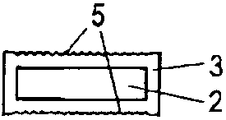
도 1 에 도시된 바와 같은, 제 1 실시형태에 따르면, 전기적 연결 소자 (1) 는, 코어로서 설계된 전기 커넥터 (2) 로 이루어져 있다. 전기 전도체 (2) 에는, 예컨대 땜납가능한 재료를 함유할 수 있는 코팅 (3) 이 전체 둘레에 제공된다. 다른 안으로서, 또한 코팅 (3) 은 접착제를 함유할 수 있다. 코팅 (3) 은, 롤링, 그라인딩, 에칭 등에 의해 형성될 수 있는 구조체 또는 거친 면 (5) 을 가진다. 따라서, 상기 코팅의 유효 면적은 이러한 공정 단계가 없는 상기 코팅의 유효 면적 보다 크다.According to the first embodiment, as shown in FIG. 1, the electrical connecting
도 2 에 도시된 바와 같은, 제 2 실시형태에 따르면, 전기 커넥터 소자 (1) 는, 편평한 와이어로서 설계된 전기 전도체 (2) 로 이루어져 있다. 상기 전기 전도체는, 비원형이며 본질적으로 사각형인 단면을 가진다. 도 2a 및 도 2b 에 도시된 바와 같이, 전기 커넥터 (2) 의 상부측에는, 마찬가지로 전기 전도성인 코팅이 제공되어 있다. 도 2a 및 도 2b 에 도시된 바와 같은, 전기 전도체 (2) 의 상부측, 즉 코팅 (3) 의 상측은 구조체 또는 거친 면 (5) 을 갖는다. 다른안으로서, 도 2a 및 도 2b 에 도시된 바와 같이, 전기 전도체 (2) 의 하부측 또한 코팅을 가질 수 있다.According to the second embodiment, as shown in FIG. 2, the
도 3 에 도시된 바와 같은, 제 3 실시형태에 따르면, 전기적 연결 소자 (1) 는, 도 2 에 따른 실시형태 예와 유사한 편평한 와이어로서 설계된 전기 전도체 (2) 로 이루어져 있다. 도 3 에 도시된 코팅 (3) 은 전기 연결 소자 (1) 의 상부측 및 바닥측에 구조체 및/또는 거친 면 (5) 을 갖는다. 전기 전도체 (2) 의 전체 외주에 걸친 단면에 코팅 (3) 이 또한 적용됨에 따라, 전기적 연결 소자의 범용성이 얻어진다. 상기 가공 동안에는, 상기 전기적 연결 소자 (1) 의 정확한 위치에 주의를 기울일 필요가 없다. 또한, 상기 전기적 연결 소자는 해로운 주위의 영향 및 부식에 보호된다. 이러한 맥락에서, 상기 코팅은 동일한 두께로 형성될 필요가 없다. 오히려, 보다 많은 코팅재가 예컨대, 일측에 적용될 수 있다. 다른 측에는 층 두께가 예컨대 감소된다. 특히 바람직한 방법에 있어서, 접촉을 위한 측에서의 층 두께는, 코팅이 주로 보호 기능을 하는 대향 측에서의 층 두께 보다 크다.According to the third embodiment, as shown in FIG. 3, the
도 4 에 도시된 바와 같은, 제 4 실시형태에 따르면, 전기적 연결 소자 (1) 는, 도 2 및 도 3 에 따른 실시형태와 유사한 편평한 와이어로서 구성된 전기 전도체 (2) 로 이루어져 있다. 그러나, 여기서, 코팅 (3) 의 표면은 에너지 흡수를 목적으로 한 전기 전도체 (2) 의 측에서만 변경이 이루어져 있다. 그래서, 구조체 및/또는 거친 면 (5) 은 코팅의 외주부에만 걸친 단면에 뻗어있다. 그러나, 코팅 (3) 은 전체 외주에 걸친 단면에 위치하여, 전기 전도체 (2) 는 코팅 (3) 에 의해 완전히 감싸지게 된다. 이로 인하여, 전기 전도체 (2) 는 환경적 영향 및 부식에 대하여 보호될 수 있다. 또한, 이러한 경우에, 모든 위치에서 동일한 두께로 이루어질 필요가 없다. 오히려, 보다 많은 코팅재가 예컨대, 일 측에 적용될 수 있다. 다른 측에서, 상기 층 두께는 예컨대 감소된다. 특히 유리한 방식으로, 상기 층 두께는, 코팅이 주로 보호 기능을 하는 대향 측 보다 접촉이 이루어지는 측에서 크다.According to the fourth embodiment, as shown in FIG. 4, the
본 발명에 따른 전기적 연결 소자를 사용한 것은 도 5 를 참조로 이하에 설명할 것이다. 이러한 경우에, 도 5 의 전기적 연결 소자는, 편평한 와이어로서 설계된 전기 전도체 (2) 를 가진다. 상기 전기적 연결 소자는, 에너지 입력 장치의 방향으로 상기 코팅이 구조체 및/또는 거친 면 (5) 을 가지는 측에 배치되는 방식으로, 전기 요소 (4), 예컨대 솔라셀 상에 적용된다. 상기 에너지 입력 장치는, 안정적인 연결을 이루기 위하여 코팅재를 충분히 가열할 수 있는 임의의 형태의 장치일 수 있다. 도 5 는 편평한 와이어로서 설계된 전기 전도체 (2) 가 전체 둘레에 코팅을 가지는 연결 소자를 나타낸다. 또한, 상기 코팅이 연결 소자 (1) 의 양 측에 구조체 및/또는 거친 면 (5) 을 가짐에 따라, 상기 연결 소자 (1) 는 도시된 위치 뿐만아니라 180°반전된 위치에도 적용될 수 있다. 코팅 (3) 이 땜납 가능한 재료로 이루어질 때, 상기 코팅은 예컨대, 적외선 광에 의해 가열되어 녹게 된다. 이로 인해, 상기 코팅은 전기 요소 (4) 와 접합되며, 냉각 후에, 전기 전도체 (2) 와 전기 요소 (4) 간의 연결이 이루어진다.The use of the electrical connection element according to the invention will be described below with reference to FIG. 5. In this case, the electrical connecting element of FIG. 5 has an
전체 실시형태에 있어서, 코팅 (3) 의 표면 (5) 은 임의의 종류의 구조체, 예컨대, 길이 방향 및/또는 횡단 방향의 홈, 길이 방향 및/또는 횡단 방향의 유체, 길이 방향 및/또는 횡단 방향의 그라인딩 마크 등을 가질 수 있다. 거친 면 (5) 은 하나 이상의 바람직한 방향을 가질 수 있거나 모든 방향에서 동일하게 설계될 수 있다. 구조체 및/또는 거친 면 (5) 은 에칭에 의해 기계적으로 및/또는 화학적으로 실행될 수 있다.In the whole embodiment, the
모든 실시형태에 있어서, 코팅 (3) 은 전기 전도체 (2) 와 전기 요소 (4) 의 연결을 위한 수단을 그 자체로 구성한다. 상기 전기적 연결 소자 (1) 를 사용할 때에, 예컨대, 땜납 또는 접착제와 같은 다른 연결 수단이 필요하지 않다.In all embodiments, the
모든 실시형태에 있어서, 코팅 (3) 은 땜납가능한 재료로 이루어질 수 있다. 코팅 (3) 의 큰 표면 (5) 은 전기 전도체 (2) 와 전기 요소 (4) 간의 땜납 연결부의 형성에 관점에서 신속히 가열할 수 있게 해준다. 상기 땜납은 자동으로 실행될 수 있다. 상기 땜납은 적외선 광에 의해 실행될 수 있다. 상기 코팅이 땜납가능한 재료, 특히 땜납, 예컨대 주석으로 이루어질 때, 상기 땜납은 추가 재료없이 실행될 수 있다. 이러한 경우에, 땜납 연결부에 필요한 상기 땜납은 코팅재 자체이다.In all embodiments, the
다른 예에 따른 전도성 코팅 (3) 이 접착제를 함유할 때, 이는 전기 전도체 (2) 와 전기 요소 (4) 의 연결을 위한 수단으로서 작용할 수 있다. 또한, 이러한 경우에, 코팅 (3) 내로 향상된 에너지가 도입되게 되어, 전기 전도체 (2) 와 전기 요소 (4) 간의 접착제 접합의 보다 신속하고 보다 안정적인 실행이 코팅 (3) 의 확대된 표면에 의해 얻어진다. When the
도 6 에 도시된 바와 같이, 전기 전도체 (2) 의 표면 (6) 은 코팅 (3) 의 표면 (5) 의 처리에 더하여 변경될 수 있다. 그래서, 전기 전도체 (2) 는 마찬가지로 구조체 및/또는 거친 면 (6) 으로 설계될 수 있다. 이로써, 전기 전도체와 코팅재 간의 확대된 접촉면이 이용될 수 있다는 점과, 이로써 얻어진 접착 강도가 증가된다는 이점을 얻는다. 예정된 접착 강도를 얻기 위한 코팅의 층 두께는 감소될 수 있다.As shown in FIG. 6, the
공지된 전기적 연결 소자 및 편평한 와이어로 설계된 연결 소자에 있어서, 코팅은 일반적으로 볼록면을 가진다. 그러나, 본 발명에 따른 연결 소자에 있어, 코팅의 표면의 처리로 인하여 코팅의 표면은 편평하고 균일하다. 따라서, 본 발명에 따른 전기적 연결 소자는 그 표면 상, 적어도 일부 영역에서 완전히 편평하거나 균일할 수 있다. 이는, 전기 요소, 예컨대 솔라 셀 상의 적용에 있어서 편평하게 놓여져, 안정적인 접합이 형성된다는 이점을 가진다. 솔라 셀 상, 특히 땜납 연결부에서 대향 접촉부로서 역할하는 임프린트된 (imprinted) 실버 버스 바 (silver bus bar) 상에 땜납될 때에, 이 재료는 완전히 균일하게 놓여지며, 이는 상당히 양호한 땜납 결과를 가져온다. In connection elements designed with known electrical connection elements and flat wires, the coating generally has a convex surface. However, in the connecting element according to the invention, the surface of the coating is flat and uniform due to the treatment of the surface of the coating. Thus, the electrical connection element according to the invention can be completely flat or uniform on its surface, at least in some areas. This has the advantage of being laid flat in applications on electrical elements such as solar cells, thus forming a stable junction. When soldered on a solar cell, in particular on an imprinted silver bus bar that serves as an opposing contact at the solder connection, the material is placed completely uniform, which results in a fairly good solder result.
또한, 상기 연결 소자, 예컨대, 편평한 와이어 (이 와이어의 코팅 또한 본질적으로 편평하고 균일한 표면을 가짐) 는 다루기가 보다 용이하다. 특히, 이러한 용도에 사용되는 진공 파지기 (gripper) 는 상기 균일한 대상물을 보다 신속하며 안정적으로 파지할 수 있다. 또한, 균일하고 편평한 표면을 지닌 와이어가 또한 코일 상에 감겨질 수 있어 보다 공간을 절약할 수 있고 빠르며 공정 안정성이 향상될 수 있다는 이점이 얻어진다. 그래서, 상기 와이어, 특히 편평한 와이어는 코일 상에 층으로 감고 풀기가 용이하다. 또한, 불규칙 권회 (winding) 의 경우에 손상될 수 있는 곧음성 (straightness) 이 유지확보될 수 있다. 이는 자동화에 대한 기계가공성에 이점을 제공하여 제조 가격에 대해 이점을 제공한다.In addition, the connecting elements, for example flat wires (the coating of which also has an essentially flat and uniform surface) are easier to handle. In particular, a vacuum gripper used for this application can grasp the uniform object more quickly and stably. In addition, the advantage that a wire having a uniform and flat surface can also be wound on the coil, saving more space, being faster and improving process stability. Thus, the wire, in particular flat wire, is easy to wind up and loosen in layers on the coil. In addition, straightness that can be damaged in case of irregular winding can be maintained. This provides an advantage in machinability for automation and therefore in manufacturing costs.
본 발명에 따른 전기적 연결 소자 (1) 는 특히 유리한 방식으로 솔라 셀 (4) 에 대한 커넥터로서 사용될 수 있다. 도 7 에 도시된 바와 같이, 예컨대, 편평한 와이어로서 설계된 두 개의 연결 소자 (1) 가 솔라셀 (4) 의 표면 상에 적용된다. 다른안으로서, 본 발명에 따른 달리 설명된 연결 소자 또한 사용될 수 있다. 솔라셀에 대한 커넥터로서, 구조체 또는 거친 면을 지닌 전기 전도체를 가지는 연결 소자를 사용할 때에, 상기 솔라셀로부터 연결 소자를 제거하기 위해서, 높은 벗김력 (strip off force) 또는 분리력 (tear off force) 이 요구된다. 또한, 규정된 벗김력 또는 절단력에 대한 코팅 두께를 감소시킬 수도 있다.The
몇 개의 솔라셀 (4) 은 연결 소자 (1) 에 의해 임의의 적절한 방식으로 솔라 모듈 (7) 과 서로 연결될 수 있다. 편평한 와이어로서 설계된 연결 소자 (1) 를 사용할 때에, 연속적인 연결 밴드를 지닌 도 8 에 도시된 외관이 얻어진다. 다른안으로서, 본 발명에 따라 달리 설명된 연결 소자 또한 사용될 수 있으며, 여기서 예컨대, 펀치 가공 또는 컷 밴드를 사용하여 연결이 이루어질 때에는 연속적인 연결 밴드를 볼 수 없다.Several
솔라 모듈 (7) 의 두 개의 인접 솔라셀 (4) 을 연결시키는 것이 도 8 에 나타나 있다. 이러한 경우에, 솔라셀 (4) 의 각각의 상부측은, 본 발명에 따른 연결 소자 (1) 에 의해 인접 솔라셀 (4) 의 바닥측과 연결된다.Connecting two adjacent
본 발명에 따른 다른 실시형태는 상기 설명된 특징의 일부만을 가지며, 특징들의 각각의 조합, 특히 달리 설명된 실시형태로부터의 특징들의 각각의 조합을 고려해 볼 수 있다.Other embodiments according to the invention have only some of the features described above and one can contemplate each combination of features, in particular each combination of features from alternatively described embodiments.
Claims (21)
Applications Claiming Priority (2)
| Application Number | Priority Date | Filing Date | Title |
|---|---|---|---|
| AT0093905A AT502004B1 (en) | 2005-06-01 | 2005-06-01 | ELECTRICAL CONNECTING ELEMENT, METHOD FOR THE PRODUCTION THEREOF AND SOLAR CELL AND MODULE WITH CONNECTING ELEMENT |
| ATA939/2005 | 2005-06-01 |
Publications (1)
| Publication Number | Publication Date |
|---|---|
| KR20080034858A true KR20080034858A (en) | 2008-04-22 |
Family
ID=36888748
Family Applications (1)
| Application Number | Title | Priority Date | Filing Date |
|---|---|---|---|
| KR1020077030995A KR20080034858A (en) | 2005-06-01 | 2006-05-29 | Electrical connecting element |
Country Status (6)
| Country | Link |
|---|---|
| EP (1) | EP1891701A1 (en) |
| JP (1) | JP2008543062A (en) |
| KR (1) | KR20080034858A (en) |
| CN (1) | CN101199084A (en) |
| AT (1) | AT502004B1 (en) |
| WO (1) | WO2006128204A1 (en) |
Cited By (4)
| Publication number | Priority date | Publication date | Assignee | Title |
|---|---|---|---|---|
| WO2016190602A1 (en) * | 2015-05-22 | 2016-12-01 | 엘에스전선 주식회사 | Ring-shaped wire for solar cell module |
| KR101692167B1 (en) * | 2015-12-01 | 2017-01-03 | 엘에스전선 주식회사 | Circular wire for solar cell module |
| KR20180049835A (en) * | 2016-11-03 | 2018-05-14 | 엘에스전선 주식회사 | Solder composition for circular wire of solar cell module and cirfular wire for solar cell module having a solder plating layer formed from the same |
| WO2018097576A1 (en) * | 2016-11-22 | 2018-05-31 | 한화첨단소재 주식회사 | Glass-integrated protective substrate for glass-to-glass solar cell, protection substrate pair for glass-to-glass solar cell, solar cell module and manufacturing method thereof |
Families Citing this family (7)
| Publication number | Priority date | Publication date | Assignee | Title |
|---|---|---|---|---|
| JP2010205792A (en) * | 2009-02-27 | 2010-09-16 | Hitachi Cable Ltd | Solar cell lead, method of manufacturing same, and solar cell using same |
| JP2012124375A (en) * | 2010-12-09 | 2012-06-28 | Sony Chemical & Information Device Corp | Solar cell module and method for manufacturing the same |
| JP5415396B2 (en) * | 2010-12-22 | 2014-02-12 | デクセリアルズ株式会社 | Solar cell module manufacturing method and solar cell module |
| EP2615647B1 (en) | 2011-06-28 | 2017-02-22 | Panasonic Intellectual Property Management Co., Ltd. | Solar cell module |
| KR101890324B1 (en) * | 2012-06-22 | 2018-09-28 | 엘지전자 주식회사 | Solar cell module and ribbon assembly |
| EP3392916A1 (en) * | 2017-04-19 | 2018-10-24 | Heraeus Deutschland GmbH & Co. KG | Ageing-resistant aluminium connector for solar cells |
| EP3447804B1 (en) * | 2017-08-25 | 2022-02-16 | Heraeus Deutschland GmbH & Co. KG | Solar cell connector with functional longitudinal coating |
Family Cites Families (11)
| Publication number | Priority date | Publication date | Assignee | Title |
|---|---|---|---|---|
| JPS604270A (en) * | 1983-06-22 | 1985-01-10 | Hitachi Ltd | Manufacture of solar battery |
| ITVR940013A1 (en) * | 1994-02-22 | 1995-08-22 | Uteco Spa Flexo & Converting M | INK DEVICE FOR ROTARY OFFSET RIBBON PRINTERS |
| JPH09293754A (en) * | 1996-04-24 | 1997-11-11 | Canon Inc | Electric circuit part, manufacture thereof, conductive ball, conductive connection member, and manufacture thereof |
| JPH09321425A (en) * | 1996-05-28 | 1997-12-12 | Nippon Antomu Kogyo Kk | Mounting method for chip-type electronic component |
| JPH1121660A (en) * | 1997-07-03 | 1999-01-26 | Hitachi Cable Ltd | Connecting wire for solar battery |
| US6294255B1 (en) * | 1998-06-29 | 2001-09-25 | Yazaki Corporation | Method of and structure for fixing a flexible electrical conductor |
| US6833526B2 (en) * | 2001-03-28 | 2004-12-21 | Visteon Global Technologies, Inc. | Flex to flex soldering by diode laser |
| JP2002313604A (en) * | 2001-04-18 | 2002-10-25 | Tdk Corp | Polymer ptc device |
| DE10137778A1 (en) * | 2001-08-02 | 2003-03-06 | Siemens Und Shell Solar Gmbh | Method for contacting thin-film electrodes |
| JP2004363293A (en) * | 2003-06-04 | 2004-12-24 | Sharp Corp | Solar cell module and manufacturing method thereof |
| JP4356417B2 (en) * | 2003-10-10 | 2009-11-04 | 日立電線株式会社 | Copper alloy wire for electronic parts |
-
2005
- 2005-06-01 AT AT0093905A patent/AT502004B1/en not_active IP Right Cessation
-
2006
- 2006-05-29 EP EP06741017A patent/EP1891701A1/en not_active Withdrawn
- 2006-05-29 CN CNA2006800194231A patent/CN101199084A/en active Pending
- 2006-05-29 JP JP2008513863A patent/JP2008543062A/en active Pending
- 2006-05-29 WO PCT/AT2006/000218 patent/WO2006128204A1/en active Application Filing
- 2006-05-29 KR KR1020077030995A patent/KR20080034858A/en not_active Application Discontinuation
Cited By (4)
| Publication number | Priority date | Publication date | Assignee | Title |
|---|---|---|---|---|
| WO2016190602A1 (en) * | 2015-05-22 | 2016-12-01 | 엘에스전선 주식회사 | Ring-shaped wire for solar cell module |
| KR101692167B1 (en) * | 2015-12-01 | 2017-01-03 | 엘에스전선 주식회사 | Circular wire for solar cell module |
| KR20180049835A (en) * | 2016-11-03 | 2018-05-14 | 엘에스전선 주식회사 | Solder composition for circular wire of solar cell module and cirfular wire for solar cell module having a solder plating layer formed from the same |
| WO2018097576A1 (en) * | 2016-11-22 | 2018-05-31 | 한화첨단소재 주식회사 | Glass-integrated protective substrate for glass-to-glass solar cell, protection substrate pair for glass-to-glass solar cell, solar cell module and manufacturing method thereof |
Also Published As
| Publication number | Publication date |
|---|---|
| AT502004B1 (en) | 2007-07-15 |
| CN101199084A (en) | 2008-06-11 |
| WO2006128204A1 (en) | 2006-12-07 |
| AT502004A1 (en) | 2006-12-15 |
| JP2008543062A (en) | 2008-11-27 |
| EP1891701A1 (en) | 2008-02-27 |
Similar Documents
| Publication | Publication Date | Title |
|---|---|---|
| KR20080026568A (en) | Electrical connection element | |
| KR20080034858A (en) | Electrical connecting element | |
| US7476800B2 (en) | Electric connection element | |
| JP2008543003A5 (en) | ||
| TWI422076B (en) | Semiconductor arrangement and method for manufacturing semiconductor arrangement | |
| US20110096507A1 (en) | Microelectronic thermal interface | |
| JP2008543062A5 (en) | ||
| CA2697958A1 (en) | Buss bar strip | |
| US20140246068A1 (en) | Metal connector profile, solar module and method for its manufacture | |
| WO2008027167A1 (en) | Clad aluminum connector | |
| GB2373206A (en) | Bonding electric wires using ultrasonic vibrations | |
| US20060272843A1 (en) | Electric connection element | |
| BRPI0907493A2 (en) | Process for manufacturing a thin layer deposit heating element on an insulating substrate and the obtained element | |
| EP0974929B1 (en) | Chip card and method of manufacturing a chip card | |
| EP2989662B1 (en) | Back-contact back-sheet for photovoltaic modules with pass-through electric contacts | |
| CN107146826B (en) | Composite welding strip | |
| CN111403296B (en) | Semiconductor packaging piece and manufacturing method thereof | |
| EP3078245B1 (en) | Method for producing a power printed circuit and power printed circuit obtained by this method | |
| CN104810327A (en) | Structure and formation method of chip package structure | |
| EA017970B1 (en) | Bus bar and panel of laminated glass | |
| CN206490053U (en) | The framework of diode (led) module | |
| RU2005107863A (en) | THICK-FILM CONTACT SILICON PHOTOELECTRIC CONVERTER AND METHOD FOR PRODUCING IT | |
| WO2003012883A3 (en) | Method for contacting thin-film electrodes | |
| JP2002025357A (en) | Extr-fine coaxial cable, extr-fine coaxial flat cable, processed electric wire and manufacturing method of the same | |
| CN205378366U (en) | Be used as insulation board of baffle when pressfitting circuit board |
Legal Events
| Date | Code | Title | Description |
|---|---|---|---|
| WITN | Application deemed withdrawn, e.g. because no request for examination was filed or no examination fee was paid |