EP2989662B1 - Back-contact back-sheet for photovoltaic modules with pass-through electric contacts - Google Patents
Back-contact back-sheet for photovoltaic modules with pass-through electric contacts Download PDFInfo
- Publication number
- EP2989662B1 EP2989662B1 EP14731004.9A EP14731004A EP2989662B1 EP 2989662 B1 EP2989662 B1 EP 2989662B1 EP 14731004 A EP14731004 A EP 14731004A EP 2989662 B1 EP2989662 B1 EP 2989662B1
- Authority
- EP
- European Patent Office
- Prior art keywords
- contact
- sheet
- photovoltaic module
- connecting element
- layer
- Prior art date
- Legal status (The legal status is an assumption and is not a legal conclusion. Google has not performed a legal analysis and makes no representation as to the accuracy of the status listed.)
- Active
Links
- 239000000758 substrate Substances 0.000 claims description 80
- 239000004020 conductor Substances 0.000 claims description 55
- 239000000463 material Substances 0.000 claims description 48
- 238000000034 method Methods 0.000 claims description 46
- 238000004519 manufacturing process Methods 0.000 claims description 27
- XAGFODPZIPBFFR-UHFFFAOYSA-N aluminium Chemical compound [Al] XAGFODPZIPBFFR-UHFFFAOYSA-N 0.000 claims description 24
- 229910052782 aluminium Inorganic materials 0.000 claims description 21
- 239000000853 adhesive Substances 0.000 claims description 18
- 230000001070 adhesive effect Effects 0.000 claims description 17
- RYGMFSIKBFXOCR-UHFFFAOYSA-N Copper Chemical compound [Cu] RYGMFSIKBFXOCR-UHFFFAOYSA-N 0.000 claims description 16
- 229910052802 copper Inorganic materials 0.000 claims description 15
- 239000010949 copper Substances 0.000 claims description 15
- 239000004411 aluminium Substances 0.000 claims description 12
- 229920003023 plastic Polymers 0.000 claims description 11
- 239000004033 plastic Substances 0.000 claims description 11
- 238000004891 communication Methods 0.000 claims description 5
- 238000012545 processing Methods 0.000 claims description 5
- 229910000881 Cu alloy Inorganic materials 0.000 claims description 4
- 229910000838 Al alloy Inorganic materials 0.000 claims description 3
- OKTJSMMVPCPJKN-UHFFFAOYSA-N Carbon Chemical compound [C] OKTJSMMVPCPJKN-UHFFFAOYSA-N 0.000 claims description 2
- 229910052799 carbon Inorganic materials 0.000 claims description 2
- 229920001971 elastomer Polymers 0.000 claims description 2
- 239000000806 elastomer Substances 0.000 claims description 2
- 239000013536 elastomeric material Substances 0.000 claims description 2
- 239000007769 metal material Substances 0.000 claims description 2
- 238000004080 punching Methods 0.000 claims description 2
- 230000008878 coupling Effects 0.000 claims 2
- 238000010168 coupling process Methods 0.000 claims 2
- 238000005859 coupling reaction Methods 0.000 claims 2
- AZDRQVAHHNSJOQ-UHFFFAOYSA-N alumane Chemical group [AlH3] AZDRQVAHHNSJOQ-UHFFFAOYSA-N 0.000 claims 1
- 239000010410 layer Substances 0.000 description 125
- 230000008569 process Effects 0.000 description 15
- 229910052751 metal Inorganic materials 0.000 description 13
- 239000002184 metal Substances 0.000 description 13
- 238000003825 pressing Methods 0.000 description 13
- BQCADISMDOOEFD-UHFFFAOYSA-N Silver Chemical compound [Ag] BQCADISMDOOEFD-UHFFFAOYSA-N 0.000 description 12
- 239000010408 film Substances 0.000 description 12
- 229910052709 silver Inorganic materials 0.000 description 12
- 239000004332 silver Substances 0.000 description 12
- 238000003466 welding Methods 0.000 description 12
- 239000011159 matrix material Substances 0.000 description 10
- -1 for example Polymers 0.000 description 9
- 238000003475 lamination Methods 0.000 description 9
- 230000014509 gene expression Effects 0.000 description 7
- 229920000642 polymer Polymers 0.000 description 7
- 239000011241 protective layer Substances 0.000 description 7
- 241000196324 Embryophyta Species 0.000 description 6
- 239000002033 PVDF binder Substances 0.000 description 6
- 230000008901 benefit Effects 0.000 description 6
- 239000000470 constituent Substances 0.000 description 6
- 229920000139 polyethylene terephthalate Polymers 0.000 description 6
- 229920002620 polyvinyl fluoride Polymers 0.000 description 6
- 229920002981 polyvinylidene fluoride Polymers 0.000 description 6
- 239000004698 Polyethylene Substances 0.000 description 5
- 238000005452 bending Methods 0.000 description 5
- 238000007373 indentation Methods 0.000 description 5
- 229920000573 polyethylene Polymers 0.000 description 5
- PXHVJJICTQNCMI-UHFFFAOYSA-N Nickel Chemical compound [Ni] PXHVJJICTQNCMI-UHFFFAOYSA-N 0.000 description 4
- 239000004642 Polyimide Substances 0.000 description 4
- 238000002679 ablation Methods 0.000 description 4
- 230000015572 biosynthetic process Effects 0.000 description 4
- 238000000151 deposition Methods 0.000 description 4
- 239000011888 foil Substances 0.000 description 4
- 229910000510 noble metal Inorganic materials 0.000 description 4
- 229920001721 polyimide Polymers 0.000 description 4
- 238000006116 polymerization reaction Methods 0.000 description 4
- 230000001681 protective effect Effects 0.000 description 4
- 239000002344 surface layer Substances 0.000 description 4
- QVGXLLKOCUKJST-UHFFFAOYSA-N atomic oxygen Chemical compound [O] QVGXLLKOCUKJST-UHFFFAOYSA-N 0.000 description 3
- 238000005219 brazing Methods 0.000 description 3
- 239000003795 chemical substances by application Substances 0.000 description 3
- 238000005229 chemical vapour deposition Methods 0.000 description 3
- 230000000875 corresponding effect Effects 0.000 description 3
- 230000008021 deposition Effects 0.000 description 3
- PCHJSUWPFVWCPO-UHFFFAOYSA-N gold Chemical compound [Au] PCHJSUWPFVWCPO-UHFFFAOYSA-N 0.000 description 3
- 229910052737 gold Inorganic materials 0.000 description 3
- 239000010931 gold Substances 0.000 description 3
- 238000012986 modification Methods 0.000 description 3
- 230000004048 modification Effects 0.000 description 3
- 230000001590 oxidative effect Effects 0.000 description 3
- 239000001301 oxygen Substances 0.000 description 3
- 229910052760 oxygen Inorganic materials 0.000 description 3
- 239000002356 single layer Substances 0.000 description 3
- 239000010409 thin film Substances 0.000 description 3
- IJGRMHOSHXDMSA-UHFFFAOYSA-N Atomic nitrogen Chemical compound N#N IJGRMHOSHXDMSA-UHFFFAOYSA-N 0.000 description 2
- CURLTUGMZLYLDI-UHFFFAOYSA-N Carbon dioxide Chemical compound O=C=O CURLTUGMZLYLDI-UHFFFAOYSA-N 0.000 description 2
- ATJFFYVFTNAWJD-UHFFFAOYSA-N Tin Chemical compound [Sn] ATJFFYVFTNAWJD-UHFFFAOYSA-N 0.000 description 2
- XTXRWKRVRITETP-UHFFFAOYSA-N Vinyl acetate Chemical compound CC(=O)OC=C XTXRWKRVRITETP-UHFFFAOYSA-N 0.000 description 2
- 230000003667 anti-reflective effect Effects 0.000 description 2
- 230000004888 barrier function Effects 0.000 description 2
- 230000007423 decrease Effects 0.000 description 2
- 238000013461 design Methods 0.000 description 2
- 230000000694 effects Effects 0.000 description 2
- 230000007613 environmental effect Effects 0.000 description 2
- 230000003628 erosive effect Effects 0.000 description 2
- 239000007789 gas Substances 0.000 description 2
- 239000011521 glass Substances 0.000 description 2
- 238000010438 heat treatment Methods 0.000 description 2
- 238000003780 insertion Methods 0.000 description 2
- 230000037431 insertion Effects 0.000 description 2
- 239000011810 insulating material Substances 0.000 description 2
- 230000001788 irregular Effects 0.000 description 2
- 229920004889 linear high-density polyethylene Polymers 0.000 description 2
- 238000003701 mechanical milling Methods 0.000 description 2
- 229910001092 metal group alloy Inorganic materials 0.000 description 2
- 238000001465 metallisation Methods 0.000 description 2
- 229910052759 nickel Inorganic materials 0.000 description 2
- 239000011368 organic material Substances 0.000 description 2
- 230000003647 oxidation Effects 0.000 description 2
- 238000007254 oxidation reaction Methods 0.000 description 2
- 239000003755 preservative agent Substances 0.000 description 2
- 230000002335 preservative effect Effects 0.000 description 2
- 239000004065 semiconductor Substances 0.000 description 2
- 238000004381 surface treatment Methods 0.000 description 2
- 229910052718 tin Inorganic materials 0.000 description 2
- XMTQQYYKAHVGBJ-UHFFFAOYSA-N 3-(3,4-DICHLOROPHENYL)-1,1-DIMETHYLUREA Chemical compound CN(C)C(=O)NC1=CC=C(Cl)C(Cl)=C1 XMTQQYYKAHVGBJ-UHFFFAOYSA-N 0.000 description 1
- VGGSQFUCUMXWEO-UHFFFAOYSA-N Ethene Chemical compound C=C VGGSQFUCUMXWEO-UHFFFAOYSA-N 0.000 description 1
- 239000005977 Ethylene Substances 0.000 description 1
- 241000587161 Gomphocarpus Species 0.000 description 1
- UFHFLCQGNIYNRP-UHFFFAOYSA-N Hydrogen Chemical compound [H][H] UFHFLCQGNIYNRP-UHFFFAOYSA-N 0.000 description 1
- 229920010126 Linear Low Density Polyethylene (LLDPE) Polymers 0.000 description 1
- 238000005299 abrasion Methods 0.000 description 1
- 239000000654 additive Substances 0.000 description 1
- PNEYBMLMFCGWSK-UHFFFAOYSA-N aluminium oxide Inorganic materials [O-2].[O-2].[O-2].[Al+3].[Al+3] PNEYBMLMFCGWSK-UHFFFAOYSA-N 0.000 description 1
- WPPDFTBPZNZZRP-UHFFFAOYSA-N aluminum copper Chemical compound [Al].[Cu] WPPDFTBPZNZZRP-UHFFFAOYSA-N 0.000 description 1
- 238000013459 approach Methods 0.000 description 1
- 239000012298 atmosphere Substances 0.000 description 1
- 239000001569 carbon dioxide Substances 0.000 description 1
- 229910002092 carbon dioxide Inorganic materials 0.000 description 1
- 238000006243 chemical reaction Methods 0.000 description 1
- 229910017052 cobalt Inorganic materials 0.000 description 1
- 239000010941 cobalt Substances 0.000 description 1
- GUTLYIVDDKVIGB-UHFFFAOYSA-N cobalt atom Chemical compound [Co] GUTLYIVDDKVIGB-UHFFFAOYSA-N 0.000 description 1
- 230000001276 controlling effect Effects 0.000 description 1
- 229920001577 copolymer Polymers 0.000 description 1
- 230000002596 correlated effect Effects 0.000 description 1
- 230000001419 dependent effect Effects 0.000 description 1
- 230000001627 detrimental effect Effects 0.000 description 1
- 238000010292 electrical insulation Methods 0.000 description 1
- 238000007765 extrusion coating Methods 0.000 description 1
- 239000002803 fossil fuel Substances 0.000 description 1
- 239000001257 hydrogen Substances 0.000 description 1
- 229910052739 hydrogen Inorganic materials 0.000 description 1
- 230000001939 inductive effect Effects 0.000 description 1
- 238000005304 joining Methods 0.000 description 1
- 238000010030 laminating Methods 0.000 description 1
- FPYJFEHAWHCUMM-UHFFFAOYSA-N maleic anhydride Chemical compound O=C1OC(=O)C=C1 FPYJFEHAWHCUMM-UHFFFAOYSA-N 0.000 description 1
- 238000002844 melting Methods 0.000 description 1
- 230000008018 melting Effects 0.000 description 1
- 150000002739 metals Chemical class 0.000 description 1
- 238000003801 milling Methods 0.000 description 1
- 238000001451 molecular beam epitaxy Methods 0.000 description 1
- 238000003032 molecular docking Methods 0.000 description 1
- 229910052757 nitrogen Inorganic materials 0.000 description 1
- 239000000615 nonconductor Substances 0.000 description 1
- 238000000059 patterning Methods 0.000 description 1
- 238000000206 photolithography Methods 0.000 description 1
- 238000000623 plasma-assisted chemical vapour deposition Methods 0.000 description 1
- 238000007747 plating Methods 0.000 description 1
- 229920000098 polyolefin Polymers 0.000 description 1
- 229920002635 polyurethane Polymers 0.000 description 1
- 239000004814 polyurethane Substances 0.000 description 1
- 230000005855 radiation Effects 0.000 description 1
- 238000002310 reflectometry Methods 0.000 description 1
- 238000009877 rendering Methods 0.000 description 1
- 238000007650 screen-printing Methods 0.000 description 1
- 238000012216 screening Methods 0.000 description 1
- 238000005476 soldering Methods 0.000 description 1
- 239000000126 substance Substances 0.000 description 1
- 229910052715 tantalum Inorganic materials 0.000 description 1
- GUVRBAGPIYLISA-UHFFFAOYSA-N tantalum atom Chemical compound [Ta] GUVRBAGPIYLISA-UHFFFAOYSA-N 0.000 description 1
- 229920001897 terpolymer Polymers 0.000 description 1
- 238000007736 thin film deposition technique Methods 0.000 description 1
- XLYOFNOQVPJJNP-UHFFFAOYSA-N water Chemical compound O XLYOFNOQVPJJNP-UHFFFAOYSA-N 0.000 description 1
Images


Classifications
-
- H—ELECTRICITY
- H01—ELECTRIC ELEMENTS
- H01L—SEMICONDUCTOR DEVICES NOT COVERED BY CLASS H10
- H01L31/00—Semiconductor devices sensitive to infrared radiation, light, electromagnetic radiation of shorter wavelength or corpuscular radiation and specially adapted either for the conversion of the energy of such radiation into electrical energy or for the control of electrical energy by such radiation; Processes or apparatus specially adapted for the manufacture or treatment thereof or of parts thereof; Details thereof
- H01L31/02—Details
- H01L31/02002—Arrangements for conducting electric current to or from the device in operations
- H01L31/02005—Arrangements for conducting electric current to or from the device in operations for device characterised by at least one potential jump barrier or surface barrier
- H01L31/02008—Arrangements for conducting electric current to or from the device in operations for device characterised by at least one potential jump barrier or surface barrier for solar cells or solar cell modules
- H01L31/02013—Arrangements for conducting electric current to or from the device in operations for device characterised by at least one potential jump barrier or surface barrier for solar cells or solar cell modules comprising output lead wires elements
-
- H—ELECTRICITY
- H01—ELECTRIC ELEMENTS
- H01L—SEMICONDUCTOR DEVICES NOT COVERED BY CLASS H10
- H01L31/00—Semiconductor devices sensitive to infrared radiation, light, electromagnetic radiation of shorter wavelength or corpuscular radiation and specially adapted either for the conversion of the energy of such radiation into electrical energy or for the control of electrical energy by such radiation; Processes or apparatus specially adapted for the manufacture or treatment thereof or of parts thereof; Details thereof
- H01L31/02—Details
- H01L31/0224—Electrodes
- H01L31/022408—Electrodes for devices characterised by at least one potential jump barrier or surface barrier
- H01L31/022425—Electrodes for devices characterised by at least one potential jump barrier or surface barrier for solar cells
- H01L31/022441—Electrode arrangements specially adapted for back-contact solar cells
- H01L31/02245—Electrode arrangements specially adapted for back-contact solar cells for metallisation wrap-through [MWT] type solar cells
-
- H—ELECTRICITY
- H01—ELECTRIC ELEMENTS
- H01L—SEMICONDUCTOR DEVICES NOT COVERED BY CLASS H10
- H01L31/00—Semiconductor devices sensitive to infrared radiation, light, electromagnetic radiation of shorter wavelength or corpuscular radiation and specially adapted either for the conversion of the energy of such radiation into electrical energy or for the control of electrical energy by such radiation; Processes or apparatus specially adapted for the manufacture or treatment thereof or of parts thereof; Details thereof
- H01L31/04—Semiconductor devices sensitive to infrared radiation, light, electromagnetic radiation of shorter wavelength or corpuscular radiation and specially adapted either for the conversion of the energy of such radiation into electrical energy or for the control of electrical energy by such radiation; Processes or apparatus specially adapted for the manufacture or treatment thereof or of parts thereof; Details thereof adapted as photovoltaic [PV] conversion devices
- H01L31/042—PV modules or arrays of single PV cells
- H01L31/048—Encapsulation of modules
- H01L31/049—Protective back sheets
-
- H—ELECTRICITY
- H01—ELECTRIC ELEMENTS
- H01L—SEMICONDUCTOR DEVICES NOT COVERED BY CLASS H10
- H01L31/00—Semiconductor devices sensitive to infrared radiation, light, electromagnetic radiation of shorter wavelength or corpuscular radiation and specially adapted either for the conversion of the energy of such radiation into electrical energy or for the control of electrical energy by such radiation; Processes or apparatus specially adapted for the manufacture or treatment thereof or of parts thereof; Details thereof
- H01L31/04—Semiconductor devices sensitive to infrared radiation, light, electromagnetic radiation of shorter wavelength or corpuscular radiation and specially adapted either for the conversion of the energy of such radiation into electrical energy or for the control of electrical energy by such radiation; Processes or apparatus specially adapted for the manufacture or treatment thereof or of parts thereof; Details thereof adapted as photovoltaic [PV] conversion devices
- H01L31/042—PV modules or arrays of single PV cells
- H01L31/05—Electrical interconnection means between PV cells inside the PV module, e.g. series connection of PV cells
- H01L31/0504—Electrical interconnection means between PV cells inside the PV module, e.g. series connection of PV cells specially adapted for series or parallel connection of solar cells in a module
- H01L31/0516—Electrical interconnection means between PV cells inside the PV module, e.g. series connection of PV cells specially adapted for series or parallel connection of solar cells in a module specially adapted for interconnection of back-contact solar cells
-
- H—ELECTRICITY
- H01—ELECTRIC ELEMENTS
- H01L—SEMICONDUCTOR DEVICES NOT COVERED BY CLASS H10
- H01L31/00—Semiconductor devices sensitive to infrared radiation, light, electromagnetic radiation of shorter wavelength or corpuscular radiation and specially adapted either for the conversion of the energy of such radiation into electrical energy or for the control of electrical energy by such radiation; Processes or apparatus specially adapted for the manufacture or treatment thereof or of parts thereof; Details thereof
- H01L31/18—Processes or apparatus specially adapted for the manufacture or treatment of these devices or of parts thereof
-
- Y—GENERAL TAGGING OF NEW TECHNOLOGICAL DEVELOPMENTS; GENERAL TAGGING OF CROSS-SECTIONAL TECHNOLOGIES SPANNING OVER SEVERAL SECTIONS OF THE IPC; TECHNICAL SUBJECTS COVERED BY FORMER USPC CROSS-REFERENCE ART COLLECTIONS [XRACs] AND DIGESTS
- Y02—TECHNOLOGIES OR APPLICATIONS FOR MITIGATION OR ADAPTATION AGAINST CLIMATE CHANGE
- Y02E—REDUCTION OF GREENHOUSE GAS [GHG] EMISSIONS, RELATED TO ENERGY GENERATION, TRANSMISSION OR DISTRIBUTION
- Y02E10/00—Energy generation through renewable energy sources
- Y02E10/50—Photovoltaic [PV] energy
Definitions
- the present invention relates to the field of photovoltaic modules including back-contact cells.
- the present invention relates to novel back-contact back-sheets for a photovoltaic module and manufacturing methods thereof.
- the present invention relates to a back-contact back-sheet and a manufacturing method thereof which allow the electric signal to be transferred outside the photovoltaic module in a simple and effective manner.
- the present invention relates to a back-contact back-sheet and a manufacturing method thereof which allow the terminals for electrical connection towards the outside of the photovoltaic module to contact the connecting circuit to the photovoltaic cells from the surface exposed towards the inside of the photovoltaic module.
- Solar cells are used for converting solar light into electrical energy by means of the photovoltaic effect. Solar cells are, thus, one of the most promising alternative energy sources for replacing fossil fuels. Solar cells are formed of semiconductor materials and are assembled so as to form so called photovoltaic modules, which are in turn grouped in order to form photovoltaic plants to be typically installed on building roofs or the like.
- groups of solar cells are typically encapsulated by means of an encapsulating material such as a copolymer of ethylene and vinyl acetate, commonly known as EVA.
- EVA ethylene and vinyl acetate
- the encapsulating material enclosing the solar cells is then inserted between a surface layer and a base layer or back-sheet, so as to complete the photovoltaic module.
- the surface layer, or main surface of the module covers the surface of the module exposed to the sun and allows the solar light to reach the cells.
- the back-sheet carries out a multiplicity of tasks. It guarantees protection of the encapsulating material and of the solar cells from environmental agents, while simultaneously preventing the electrical connections from oxidizing. In particular, the back-sheet prevents moisture, oxygen and other factors depending on the atmospheric conditions from damaging the encapsulating material, the cells and the electrical connections.
- the back-sheet also provides for electrical insulation for the cells and the corresponding electrical circuits. Furthermore, the back-sheet has to have a high degree of opacity due to esthetic reasons and high reflectivity in the part oriented toward the sun for functional reasons.
- the electrical connection in photovoltaic modules comprising traditional solar cells occurs on both the front and the rear side of the cell.
- the front electrode i.e. the electrode exposed to the sun light
- H-patterning a technique called "H-patterning”
- shading problems are due to the presence of metallic traces screening the light incident upon the front surface of the cell.
- Traditional electric contacts thus cause the efficiency of solar cells and modules to decrease.
- Back-contact cells are a new, more efficient and cost-effective generation of photovoltaic cells, wherein the contacts with both electrodes of the cell are transferred to the rear side of the cell, i.e. onto the side not exposed to the light radiation.
- Metallization Wrap Through (MWP) cells turn out to be a particularly efficient and easy-to-implement type of back-contact cell.
- the contact to the front electrode is transferred to the rear side of the cell by means of a through-hole extending through the entire thickness of the semiconductor substrate.
- Back-contact cells pose new technological problems concerning the design and the structure of the modules adapted to accommodate them.
- the back-sheet has to be designed so as to support a connecting circuit which is brought into electrical contact with the ohmic contacts formed on the rear side of the cell. These ohmic contacts are connected to both electrodes (base and emitter) of the cell.
- One of the solutions to this problem is the so called back-contact back-sheet, which is an evolution of the traditional back-sheet, wherein the connecting circuit is implemented directly on the surface of the back-sheet facing the cell.
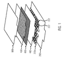
- Figure 1 the structure of a photovoltaic module comprising back-contact solar cells is shown.
- Back-contact cell 600 is arranged between an upper encapsulating material layer 450 and a lower encapsulating material layer 400. Cell 600 and encapsulating material layers 400 and 450 are then enclosed between a surface layer 800 typically made of glass or of a transparent and antireflective material and the back-sheet 200, which may be a back-contact back-sheet.
- FIG. 1 there are visible the paths of electrically conductive material making up the connecting circuit 220c to the electrodes of the solar cell. Adjacent paths are separated by channels in which the conductive material is absent. If back-sheet 200 is a back-contact back-sheet, the connecting circuit is formed directly on the surface of the lower-lying insulating substrate and is firmly fixed thereto.
- the connecting circuit 220c is used so as to ensure an electrical contact with both electrodes (i.e. with the base and the emitter) of solar cell 600.
- the paths of electrically conductive material are provided with pads 222 marking the points of the connecting circuit which are to be electrically connected with a contact area on one of the electrodes formed on the rear surface of cell 600.
- the lower encapsulating material layer 400 to be arranged between the cell 600 and the back-contact or back-contact back-sheet 200 is pierced so that, after the module has been completed, the holes formed in the lower encapsulating layer 400 correspond to areas where pads 222 for contact with the electrodes are arranged.
- the pierced encapsulating material layer 400 is then laid on top of the inner face of back-sheet or back-contact back-sheet 200, i.e. onto the face of the back-sheet or back-contact back-sheet 200 exposed towards the inside of the photovoltaic module.
- the encapsulating material foil is aligned to back-sheet or back-contact back-sheet 200 so that the holes in lower encapsulating material layer 400 correspond or are aligned to pads 222. In this manner, pads 222 are left exposed towards the inside of the photovoltaic module.
- a lump or drop of an electrically conductive material such as for example a conductive paste known as "Electro Conductive Adhesive" (ECA) is then deposited onto pads 222 of the conductive paths of connecting circuit 220c.
- ECA Electro Conductive Adhesive
- the cells 600 to be embedded in the module are placed onto the lower encapsulating material layer 400 so that each contact element on the electrodes formed on the rear surface of the cells comes into contact with a lump of conductive paste applied to one of the pads 222 and exposed to the contact with cells 600 through one of the holes of the lower encapsulating material layer 400.
- the upper encapsulating material layer 450 is then placed onto the upper surface of the cell 600, opposite the rear surface in contact with the conductive paste applied to pads 222.
- a layer 800 of a transparent and antireflective material is laid onto the upper encapsulating material layer 450.
- this can be turned upside-down and subsequently laminated in vacuum at a temperature between 145 °C and 165 °C for a time interval variable between 8 and 18 minutes.
- Figure 2a shows the structure of the module before the lamination process.
- the components of the module stacked as previously described, are singularly distinguishable.
- Figure 2a shows a stack comprising, starting from the bottom and moving towards the top of the figure, the back-sheet or back-contact back-sheet 200 with conductive pads 222 upon which conductive paste 300 has been applied, the lower encapsulating material layer 400, cells 600, the upper encapsulating material layer 450 and surface layer 800.
- contact points 620 and 640 formed on the rear side of cell 600, i.e. on the side facing connecting circuit 220c and back-sheet 200.
- Contact points 620 and 640 may be connected to the positive and negative electrode of the photovoltaic cell, respectively.
- Figure 2b schematically shows the structure of the module after the lamination process has taken place.
- the structure is arranged into a vacuum chamber from which the air is evacuated by means of pumps.
- a pressure is then applied to the structure so as to compact the layers of which the photovoltaic module structure is comprised, while simultaneously maintaining a vacuum in the area in which the module is situated.
- the whole cycle has preferably a total duration less then 18 minutes.
- the cycle preferably occurs at a temperature between 140 °C and 165 °C.
- the lamination results in hardening of the conductive paste 300 induced by polymerization, thereby causing cells 600 to attach to back-sheet 200. Furthermore, a task of the lamination process is also causing melting and subsequent polymerization of the upper and lower encapsulating material layers 450 and 400.
- interconnection terminals or busbars, are applied between the assembled module and other modules included in the photovoltaic plant.
- Fig. 3 shows a back-contact back-sheet 200 after busbars 700 for connection to a junction-box have been applied according to the prior art.
- FIG. 3 shows a back-contact back-sheet 200 after busbars 700 for connection to a junction box have been applied according to the prior art.
- Back-contact back sheet 200 is comprised of an insulating substrate 210 upon which connecting circuit 220c is fixed. Holes or " windows" 215 are formed in insulating substrate 210 so as to bring into communication the upper surface 210os of insulating substrate 210 exposed towards the air-side of the photovoltaic module with the inner surface 210is of insulating substrate 210 facing the inside of the photovoltaic module. Holes 215 extend through the whole thickness of insulating substrate 210 of the back-contact back-sheet 200 so as to reach the lower surface of connecting circuit 220c facing insulating substrate 210.
- Holes or windows 215 thus leave the lower surface of connecting circuit 220c exposed towards the air-side of the photovoltaic module and must be adequately positioned in order to enable access to the connecting circuit 220c at predetermined positions.
- the number of windows 215 thus formed are usually four: one is used for the input, one for the output, and the remaining two are used in order to permit connection to one or more respective bypass diodes.
- each busbar 700 is introduced into each window 215.
- a portion of each busbar 700 is fixed by means of soldering or other technique to the surface of connecting circuit 220c left exposed by hole 215 formed in substrate 210 of back-contact back-sheet 200.
- the operation of forming windows 215 is critical in that substrate 210 must be pierced with an extreme precision, so as to expose connecting circuit 220c, while simultaneously ensuring that the portion of circuit 220c to be exposed is not damaged during the operation of opening the windows. Therefore, when forming windows 215, an excess of ablation of substrate 210 should be avoided, which would cause connecting circuit 220c to be undesirably damaged or eroded. An undesired ablation of connecting circuit 220c would turn out to be particularly detrimental due to the limited thickness of connecting circuit 220c, usually in the range of 25 ⁇ m to 70 ⁇ m.
- busbars 700 may be hard to fix busbars 700 to connecting circuit 220c.
- Attaching busbars 700 to connecting circuit 220c is particularly critical when the two elements to be attached to each other comprise aluminum.
- the traditionally used techniques include brazing or braze welding processes requiring high temperatures.
- excessively heating the back-contact back-sheet is extremely undesirable, in that this could result in profile bending which would jeopardize the reliability of the back-contact back-sheet inside the photovoltaic module.
- the connecting circuit is implemented in aluminum
- the aluminum surface is covered by a protective thin metal film in order to prevent the exposed surface of the circuit from oxidizing, thereby permitting a correct electrical connection to the photovoltaic cell through electrically conductive paste ECA.
- This plating technique rather costly and cumbersome, should be repeated on the lower surface of the conductor in order to permit an easy connection with the busbars.
- metallization of the lower surface of the aluminum layer is preferably omitted.
- a backsheet for backcontact solar cell is disclosed in HANITA COATINGS:
- an object of the present invention is to provide a back-contact back-sheet and a method of manufacturing thereof, such that the electrical contact between the busbars and the connecting circuit may be implemented in an effective, fast and reliable manner, thus obviating the problems referred to above and related to the prior art.
- a back-contact back-sheet and a method of manufacturing thereof are proposed, based on the concept that a connecting terminal may contact the connecting circuit on the upper surface of the circuit, i.e. on the surface opposite the surface fixed to the substrate of the back-contact back-sheet.
- the back-contact back-sheet according to the present invention comprises a region indented towards the air-side of the photovoltaic module.
- the indentation is formed in a portion of the back-contact back-sheet comprising the connecting circuit.
- a through-hole is then formed within the indented region. The through-hole brings into communication the surface of the connecting circuit exposed towards the inside of the photovoltaic module with the face of the back-contact back-sheet facing the air-side of the photovoltaic module.
- a transport portion of a connecting element e.g. a rivet stem
- a connecting element e.g. a rivet stem
- the contact portion of the connecting element e.g. the head of the rivet
- the connecting element thus allows the photovoltaic module in which the back-contact back-sheet is included to exchange an electrical signal with the outside.
- current coming from another photovoltaic module in the plant may be brought into the photovoltaic module wherein the back-contact back-sheet is included.
- the current collected from the connecting circuit may be transferred outside of the photovoltaic module and sent to a junction-box.
- the contact portion of the connecting element can then be housed in the cavity defined by the indented region.
- the size dimensions of the indented region can be chosen based on the size dimensions of the contact portion of the connecting element.
- the size dimensions of the indented region can be chosen so as to be slightly greater than the respective size dimensions of the contact portion.
- the contact portion of the connecting element e.g. the rivet head
- the contact portion of the connecting element may be attached to the portion of connecting circuit included in the indented portion in such a way that, given a cross-section of the system comprising the back-contact back-sheet and the connecting element attached thereto, the contact portion of the connecting circuit is completely included in the cavity defined by the indented region.
- the depth of the cavity defined by the indented region can be advantageously chosen based on the thickness of the contact portion of the connecting element.
- the cavity defined by the indented region can be formed so that its depth is equal to or slightly greater than the thickness of the contact portion of the connecting element.
- the present invention further proposes the method of manufacturing a photovoltaic module as claimed in claim 14.
- the back-contact back-sheet according to the present invention is an evolution of the back-contact back-sheet already proposed in the previous Italian patent applications having reference numbers VI2012A000132 and VI2012A000264 .
- the back-contact back-sheet according to the present invention is substantially planar. In the figures from 6 to 12, the back-contact back-sheet, or a major portion thereof, extend across a substantially parallel plane parallel to the xy-plane.
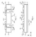
- Figures 4 and 5 show the back-contact back-sheet 200 according to two respective embodiments of the invention in an intermediate stage of the manufacturing process.
- the air-side of the photovoltaic module is the side at the bottom of Figures 4 and 5 , below the back-contact back-sheet 200 shown therein.
- back-contact back-sheet 200 comprises an outer face 200of facing the air-side of the photovoltaic module and an inner face 200if opposite the outer face 200of and exposed towards the inside of the photovoltaic module.
- Back-contact back-sheet 200 further comprises an insulating complex or substrate 210 exposed to the air-side of the photovoltaic module, as well as an electrically conductive material layer 220.
- Insulating substrate 210 has an outer surface 210os facing the air-side of the photovoltaic module and substantially coincident with the outer face 200of of back-contact back-sheet 200. Furthermore, substrate 210 has an inner surface 210is opposite outer surface 210os and facing the inside of the photovoltaic module.
- insulating substrate 210 comprises a first insulating layer 212 and a second insulating layer 216.
- the first insulating layer 212 has a surface exposed toward the air-side of the photovoltaic module substantially coincident with outer surface 210os of substrate 210.
- First insulating layer 212 is used as a barrier against moisture, UV rays, oxygen and other external environmental agents which might penetrate into the module, thereby damaging some constituent parts thereof or causing the polyurethane-like or polyester-like adhesive to degrade and turn yellow.
- First insulating layer 212 may comprise a polymer such as polyvinyl fluoride (PVF), polyvinylidene fluoride (PVDF), polyethylene terephtalate (PET), or other polymers.
- First insulating material 212 may also comprise other materials known in the state of the art.
- First insulating layer 212 may have a thickness in a range of approximately 25 to 75 ⁇ m or greater.
- Second insulating layer 216 is then applied to the inner surface of first insulating layer 212, opposite the surface exposed to the air-side.
- Second insulating layer 216 acts as an electrical insulator and a further barrier.
- Second insulating layer 216 typically comprises a polymer such as, for example, polyethylene terephtalate (PET), polyethylene (PE), polyvinyl fluoride (PVF), polyvinylidene fluoride (PVDF), polyethylene naphtalate (PEN), polyimide (PI), or the like.
- Second insulating layer 216 may have a thickness in the range of approximately 125 to approximately 350 ⁇ m or greater.
- insulating substrate 210 is comprised of a single layer comprising, for example, one or more polymers such as PET, PE, PVF, PVDF, PEN, PI, similar polymers and combinations thereof.
- substrate 210 of back-contact back-sheet 200 comprises an insulating portion 211 and a primer layer 218 applied to insulating portion 211.
- Primer layer 218 and insulating portion 211 of substrate 210 have been described in the earlier Italian patent application having filing number VI2012A000264 . In the following, only a brief summary of this embodiment will be provided.
- Insulating portion 211 of substrate 210 comprises a lower face 211lf exposed towards the air-side of the photovoltaic module and substantially coincident with outer surface 210os of substrate 210 and, thus, with outer face 200of of backc-contact back-sheet 200. Insulating portion 211 further comprises an upper face opposite lower face 211lf. Insulating portion 211 may be implemented in any of the ways in which substrate 210 can be implemented according to the embodiments described above with reference to Figure 4 .
- insulating portion 211 comprises a first insulating layer 212 and a second insulating layer 216.
- Layers 212 and 216 according to the embodiment shown in Figure 5 have analogous or identical features and functionalities to, respectively, layers 212 and 216 described with respect to the embodiment shown in Figure 4 .
- insulating portion 211 may comprise a single layer.
- the single layer or one or more of the plurality of layers making up insulating portion 211 may comprise one or more materials such as, for example, PET, PE, PVF, PVDF, PEN, PI, like polymers and combinations of the previous materials.
- Primer layer 218 is applied to the upper surface of insulating portion 211, opposite lower face 211lf, so that the inner face of primer layer 218, opposite the face facing insulating portion 211, substantially coincides with inner surface 210is of substrate 210. Primer layer 218 is arranged between lower insulating portion 211 of substrate 210 and conductive material layer 220 within which connecting circuit 220c is formed.
- Primer layer 218 may be deposited by means of extrusion coating onto the upper face of the lower insulating portion 211. Primer layer 218 may also be attached by using an adhesive system. Primer layer 218 has a thickness in the range of about 50 to about 350 ⁇ m and, preferably, in the range of about 50 to about 150 ⁇ m. Primer layer 218 carries out the main task of guaranteeing an improved adhesion of inner face 200if of the back-contact back-sheet with encapsulating material layers 400 and 450 shown in Figure 1 and/or with a thermoadesive material, which are to be applied thereupon.
- Primer layer 218 thus comprises materials which are chemically or functionally akin to the materials constituting the encapsulating material layers 400 and 450 shown in Figures 1 , 2a and 2b .
- Primer layer 218 may thus comprise EVA (for example EVA with a content of vinyl acetate variable in the range of 3% to 5%), linear low density polyethylene (LLDPE), linear high density polyethylene (LHDPE), polyolefins or combinations thereof.
- EVA for example EVA with a content of vinyl acetate variable in the range of 3% to 5%
- LLDPE linear low density polyethylene
- LHDPE linear high density polyethylene
- primer layer 218 may comprise one or more thermo-adhesive materials.
- primer layer 218 may comprise one or more of the following materials: acryl polymers or polyurethanes loaded with additives, acryl terpolymers grafted with maleic anhydride.
- back-contact back-sheet 200 comprises an electrically conductive material layer 220 applied to inner surface 210is of insulating substrate 210, so that layer 220 is firmly attached to insulating substrate 210.
- Conductive material layer 220 comprises a lower surface firmly attached to inner surface 210is of substrate 210 and an upper surface opposite the lower surface and adapted to be exposed towards the inside of the photovoltaic module.
- Conductive material layer 220 may have a thickness approximately ranging from 25 to 70 ⁇ m.
- Conductive material layer 220 comprises a metal with a high electrical conductivity such as copper or aluminium.
- Conductive material layer 220 may also comprise an alloy of copper and aluminium.
- the advantage with using aluminium instead of copper is substantially due to the lower cost of the former with respect to the latter.
- the problem with aluminium is the oxide layer, known as alumina (Al 2 O 3 ), which promptly forms as an aluminium surface is exposed to gases normally present in the atmosphere at standard pressure. Formation of an oxide layer on the upper surface of conductive layer 220 is particularly undesirable, since this surface of conductive layer 220 is to contact the electrodes of photovoltaic cells 600 through conductive adhesive 300, as describe above with reference to Figures 2a and 2b .
- a protection thin conductive film can be formed onto the upper surface of conductive material layer 220 adapted to be exposed towards the inside of the photovoltaic module.
- the protection film is deposited onto the upper surface of conductive material layer 220 in order to prevent layer 220 from oxidizing, thereby improving the electrical contact with the electrodes of the photovoltaic cells.
- the protection thin film comprises in general a metal with a high conductivity and not subject to oxidation.
- the protection thin film may comprise a metal such as, for example, copper, silver, gold.
- conductive material layer 220 comprises instead copper
- a protection conductive film comprising a metal such as, for example, nickel or tin may be formed on the surface of layer 220.
- the protection film of an electrically conductive material may be applied by following the procedure described in the earlier Italian patent application with filing number VI2012A000266 and briefly illustrated in the following.
- a connecting circuit 220c is formed within conductive material layer 220.
- Circuit 220c is comprised of metallic paths separated by channels 224.
- connecting circuit 220c is adapted to be brought into contact with both electrodes, i.e. with both base and emitter, of solar cells 600.
- pads 222 formed on conductive material paths mark the points of connecting circuit 220c which are to be electrically connected to an electrode contact formed on the surface of cell 600.
- the lower surface of connecting circuit 220c facing insulating substrate 210 is a portion of the lower surface of conductive layer 220.
- the upper surface 226 of connecting circuit 220c, opposite the lower surface and exposed towards the inside of the photovoltaic module, is a portion of the upper surface of conductive material layer 220.
- Upper surface 226 of connecting circuit 220c may comprise a protective film of an organic material (Organic Solderability Preservative) not shown in the figures.
- the organic protective film aimed at protecting the exposed surface 226 of the connecting circuit from abrasion and chemical reactions with external agents, is particularly advantageous when the connecting circuit comprises copper.
- Figures 4 and 5 show that, after connecting circuit 220c has been formed in conductive layer 220, inner face 200if of back-contact back-sheet 200 comprises upper surface 226 of connecting circuit 220c and the portion of inner surface 210is of substrate 210 left exposed by channels 224 defined by adjacent paths of connecting circuit 220c.
- Back-contact back-sheet 200 resulting from the intermediate stage of manufacturing shown in Figures 4 and 5 has a substantially planar shape across its entire extension. That is to say, outer surface 210os of substrate 210, inner surface 210is of substrate 210 and outer surface 226 of connecting circuit 220c lie each on a single respective plane, without forming any indentations or steps.
- the planes defined by the surfaces mentioned above are parallel to each other and, in Figures 4 and 5 , are parallel to the horizontal xy-plane.
- Figure 6 schematically shows a cross-section taken across a vertical plane parallel to the xz-plane of the back-contact back-sheet 200 according to the present invention in its final form.
- the substrate 210 of the back-contact back-sheet shown in Fig. 6 may be implemented in any of the ways described above with reference to Figures 4 and 5 .
- substrate 210 comprises a primer layer 218 applied on top of a lower-lying insulating portion.
- connecting circuit 220c is formed within conductive material layer 220 as indicated above with reference to Figures 4 and 5 .
- Back-contact back-sheet 200 shown in Figure 6 comprises an indented portion 250.
- the portion of inner face 200if of back-contact back-sheet 200 included in indented region 250 forms an indentation facing the air-side of the photovoltaic module.
- inner face 200if of back-contact back-sheet 200 forms a concavity facing the inside of the photovoltaic module, i.e. a concavity facing upwards with respect to the reference system of Figure 6 .
- the upper surface 256 of connecting circuit 220c and the inner surface 210is of substrate 210 form, in correspondence to indented region 250, respective cavities facing upwards.
- inner face 200if of back-contact back-sheet 200 defines a cavity 251 which, when back-contact back-sheet 200 is embedded in the photovoltaic module, communicates with the inner space of the photovoltaic module.
- outer face 200of also forms a concavity facing upwards in correspondence to indented region 250.
- Indented region 250 is formed in correspondence to connecting circuit 220c and so as to include a portion thereof.
- the portion of inner face 200if of back-contact back-sheet 200 included in indented region 250 comprises a portion of connecting circuit 220c.
- the portion of inner face 200if of back-contact back-sheet 200 included in indented region 250 comprises a portion of upper surface 226 of connecting circuit 220c.
- the whole portion of inner face 200if of back-contact back-sheet 200 included in indented region 250 includes a portion of connecting circuit 220c. That is to say, the portion of inner face 200if of back-contact back-sheet 200 included in indented region 250 does not preferably contain any portions of inner surface 210if of substrate 210.
- Figure 6 shows that the portion of inner face 200if included in indented region 250 is entirely comprised of a portion of connecting circuit 220c.
- conductive material layer 220 or connecting circuit 220c form a concavity or a cavity facing upwards, it will be assumed that upper surface 226 and the lower surface of connecting circuit 220c are substantially parallel, since connecting circuit 220c is formed from a thin, flexible film wherein the distance between upper surface 226 and the lower surface remains substantially constant.
- Indented region 250 comprises a first, substantially flat portion 252, which lies on a substantially horizontal plane P2. More precisely, the portion of upper surface 226 of connecting circuit 220c included in substantially flat portion 252 of indented region 250 lies on a substantially horizontal plane P2 parallel to the xy-plane. Furthermore, the inner surface 210is of substrate 210 included in substantially flat portion 252 of indented region 250 also lies on a plane parallel to plane P2 and, thus, on a substantially horizontal plane.
- the portion of outer surface 210os of substrate 210 included in indented region 250 lies also on a plane parallel to horizontal xy-plane.
- Flat portion 252 occupies a central area of indented region 250.
- Indented region 250 shown in Figure 6 further comprises a second, curved portion 254.
- Curved portion 254 surrounds flat portion 252 and connects it to the non-indented region of the back-contact back-sheet 200 situated around and outside indented region 250.
- Curved region 254 is such that a tangent plane to a point of inner face 200if of back-contact back-sheet 200 belonging to curved region 254 forms an angle different from zero with the horizontal xy-plane.
- the region of back-contact back-sheet 200 not included in any indented regions 250 is substantially planar, as indicated with reference to Figures 4 and 5 .
- the portion of inner face 200if of back-contact back-sheet 200 not included in any indented regions 250 lies on a substantially horizontal plane P1 lying above any given point of inner face 200if belonging to indented region 250.
- the portion of outer face 200of of back-contact back-sheet 200 not included in any indented regions 250 lies on a substantially horizontal plane lying above any point belonging to the portion of outer face 200of included in an indented region 250.
- Figure 6 shows that horizontal plane P2, defined by the portion of upper surface 226 of connecting circuit 220c included in flat portion 252 of indented region 250, lies below horizontal plane P1, defined by the portion of upper surface 226 of connecting circuit 220c not included in any indented regions 250.
- the distance between planes P1 and P2, indicated in Figure 6 by reference letter H, determines the depth of indented region 250 with respect to the non-indented region of back-contact back-sheet 200.
- indented region 250 extends through the entire thickness of back-contact back-sheet 200. That is to say, according to the embodiment shown in Figure 6 , indented region 250 extends vertically from inner face 200if to outer face 200of of back-contact back-sheet 200.
- Figure 6 shows that the portion of outer face 200of of back-contact back-sheet included in indented region 250 lies on a horizontal plane placed below the plane defined by the portion of outer face 200of of the back-contact back-sheet not included in any indented regions 250.
- the distance H between the two planes is the same as the distance between the planes P1 and P2. Therefore, according to the embodiment shown in Figure 6 , indented region 250 forms a protruding element on outer face 200of of back-contact back-sheet 200.
- the height of the protruding element is determined by depth H of cavity 251 defined by inner face 200if of back-contact back-sheet 200 in correspondence to indented region 250.
- indented region 250 is adapted to house a contact portion 720 of a connecting element 700.
- Indented region 250 is thus adapted to permit an electric contact between contact portion 720 of a connecting element 700 and connecting circuit 220c.
- contact portion 720 of connecting element 700 may advantageously be attached to the portion of upper surface 226 of connecting circuit 220c included in indented region 250, as will be described more extensively in the following.
- distance H determining the depth of cavity 251 is preferably included in the range of about 100 ⁇ m to about 800 ⁇ m. As will be explained in the following, distance H may advantageously be chosen equal or slightly greater than the thickness of contact portion 720 of connecting element 700 chosen for cooperating with back-contact back-sheet 200.
- the back-contact back-sheet 200 further comprises a through-hole 256, formed within indented portion 250.
- Hole 256 is advantageously formed within flat portion 252 of a respective indented region 250.
- hole 256 is advantageously formed in a central area of flat portion 252 of indented region 250.
- hole 256 may also advantageously be formed in a non-central position.
- Through-hole 256 is formed through the thickness of back-contact back-sheet 200 so as to extend from upper surface 226 of connecting circuit 220c to outer face 200of of back-contact back-sheet 200. It should be noticed that through-hole 256 is preferably formed in an area of back-contact back-sheet 200 such that a part of hole 256 is formed within connecting circuit 220c. Therefore, hole 256 is preferably formed so that it does not communicate with a channel 224 between two adjacent paths of connecting circuit 220c.
- hole 256 is adapted to house a transport portion 740 of a connecting element 700, so as to allow the electrical current collected from connecting circuit 220c to be transferred outside of the photovoltaic module.
- through-hole 256 has a longitudinal axis which is preferably parallel to the vertical z-axis and extends through the whole thickness of back-contact back-sheet 200.
- hole 256 communicates with the air-side of the photovoltaic module by means of lower aperture 2561a formed in outer face 200of of back-contact back-sheet 200.
- hole 256 communicates with the space included inside the photovoltaic module through upper aperture 256ua formed in upper surface 226 of connecting circuit 220c.
- hole 256 communicates, through upper aperture 256ua, with cavity 251 defined by the portion of inner face 200if of back-contact back-sheet 200 included in indented region 250.
- hole 256 extends across the horizontal x-axis by a width 256w.
- width 256w of hole 256 is in the range of about 500 ⁇ m to about 1000 ⁇ m.
- width 256w of hole 256 can be chosen so as to adapt to the thickness of transport portion 740 of connecting element 700 housed therein.
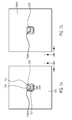
- Figures 7a and 7b show, respectively, a top view and a bottom view of a back-contact back-sheet 200 according to the present invention comprising indented region 250.
- indented region 250 is formed before processing conductive material layer 220 in order to form connecting circuit 220c. Therefore, the back-contact back-sheet shown in Figures 7a and 7b is in an intermediate stage of the manufacturing process.
- Figure 7a shows in particular that conductive material layer 220 applied to substrate 210 is formed as a full and continuous layer, whose surface does not have meanders, channels or interruptions, except for hole 256.
- the only interruption of conductive layer 220 shown in Figure 7a is hole 256 formed within indented region 250.
- Figure 7a shows that hole 256 extends along the y-axis by a length 256l.
- Length 256l of hole 256 may preferably vary in the range of a few millimetres to a few tens of millimetres.
- Figure 7b shows that outer face 200of of back-contact back-sheet 200 forms a relief or a protruding portion in correspondence to indented region 250.
- the height of the relief formed by indented region 250 on outer face 200of corresponds and is about equal to depth H of cavity 251 formed by inner face 200if in correspondence to indented region 250.
- the expression “upper surface” of indented region 250 will indicate the portion of inner face 200if of the back-contact back-sheet included in indented region 250.
- the expression “lower surface” of indented region 250 will indicate the portion of outer face 200of of the back-contact back-sheet included in indented region 250.
- the upper surface and the lower surface of indented region 250 have a substantially square shape. More specifically, Figure 7a shows that the portion of inner face 200if of back-contact back-sheet 200 included in indented region 250 is substantially square. Furthermore, Figure 7b shows that the portion of outer face 200of of back-contact back-sheet 200 included in indented region 250 is substantially square.
- indented region 250 has an upper surface or a lower surface having a form different from a square.
- the indented region may have, depending on usage requirements, the shape of a circle, a regular polygon, an irregular polygon.
- the shape of the upper surface of indented region 250 may be advantageously chosen based on the shape of contact portion 720 of connecting element 700 to be used in cooperation with the considered indented region 250, as will be explained in the following with reference to Figures 10a and 10b .
- the upper surface of indented region 250 extends preferably across an area ranging from approximately 20 to 80 mm 2 .
- the upper surface of indented region 250 has preferably an area sufficient to guarantee a current density compatible with the features of the chosen connecting element 700 and conductive connecting system. More in detail, the upper surface of indented region 250 preferably extends across an area ranging from approximately 30 to 70 mm 2 . If the upper surface of indented region 250 is square, the square side has preferably a length of 6 mm or 8 mm. Thus, the area of the upper surface of indented region 250 is preferably of about 36 mm 2 or 64 mm 2 .
- the area of the upper surface of indented region 250 may be less than 20 mm 2 or greater than 80 mm 2 , depending on the requirements and, in particular, depending on the shape and the size of contact portion 720 of connecting element 700 to be used in cooperation with back-contact back-sheet 200 and with indented region 250.
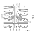
- Figure 8 shows a top view of a portion of a back-contact back-sheet 200 according to an embodiment of the invention in an intermediate stage of the manufacturing process.
- Figure 8 shows a portion of inner face 200if of back-contact back-sheet 200 in a non-final stage of the manufacturing process.
- connecting circuit 220c exposing upper surface 226 towards the outside has been formed within conductive material layer 220.
- the conductive material paths delimited by channels 224 are visible.
- Channels 224 leaves some portion of inner surface 210is of substrate 210 exposed.
- pads 222 are formed, which are adapted to electrically contact the electrodes of the photovoltaic cells.
- Figure 8 also shows that four indented regions 250a and 250b have been formed in the back-contact back-sheet.
- indented regions 250a and 250b are formed in correspondence to portions of inner face 200if of the back-coontact back-sheet occupied by connecting circuit 220c. More specifically, all four indented regions 250a and 250b are formed so that their respective surface portions included in inner face 200if of back-contact back-sheet 200 are entirely included in one of the conductive paths forming connecting circuit 220c.
- the portion of inner face 200if of back-contact back-sheet 200 included in each indented region 250a and 250b i.e. the upper surface of each indented region 250a and 250b, is exclusively comprised of a respective portion of upper surface 226 of connecting circuit 220c.
- Two of the four indented regions may be used as points of connecting circuit 220c through which an electrical signal can be exchanged with the outside of the photovoltaic module.
- the two remaining indented regions may then be used so as to permit an electrical connection to electrical components or apparatuses outside the photovoltaic module.
- each of the two remaining indented regions may be adapted to be connected to a respective diode.
- the diode is a by-pass diode. It is pointed out that the upper surface of indented regions 250a is smaller than the upper surface of indented regions 250b.
- the upper surface of indented regions 250a may be approximately square, with the square formed by each indented region 250a having a size length of about 6 mm.
- the upper surface of indented regions 250b may also be approximately square, with the square formed by each indented region 250b having a size length of about 8 mm.
- the number of indented regions 250 formed in back-contact back-sheet 200 is at least two. However, the indented regions 250 do not necessarily have to be four. In general, any number equal to or greater than two of indented regions 250 may be formed in back-contact back-sheet 200.
- back-contact back-sheet 200 takes its final form shown in Figure 6 .
- Figures 9a to 11 show some examples of how a connecting element 700 may cooperate with the back-contact back-sheet 200 according to the present invention, in order to allow the photovoltaic module including back-contact back-sheet 200 to exchange an electric signal with the outside.
- FIGS 9a and 9b show an example of a connecting element 700 which may be used so as to cooperate with back-contact back-sheet 200 according to the present invention.
- Connecting element 700 comprises a contact portion 720 and a transport portion 740 connected to contact portion 720.
- Contact portion 720 and transport portion 740 are connected by means of a connecting portion 760.
- Connection portion 760 is arranged between contact portion 720 and transport portion 740 so as to allow one to distinguish between contact portion 720 and transport portion 740.
- the surface portion of connection portion 760 extends by a width (dimension along the y-axis in Figures 9a and 9b ) much greater than its height (dimension along the z-axis in Figures 9a and 9b ).
- the surface portion of connection portion 760 thus extends along a segment belonging to both planes on which contact portion 720 and transport portion 740 lie. In Figures 9a and 9b , the segment defined by the surface portion of connection portion 760 is parallel to the y-axis.
- Contact portion 720 is adapted to be attached to upper surface 226 of connecting circuit 220c in correspondence to an indented region 250. Contact portion 720 is attached to connecting circuit 220c so as to be in electrical contact thereto.
- Transport portion 740 of connecting element 700 is instead adapted to be partially housed in one of holes 256 and, more exactly, in the hole 256 formed in the indented region 250 in which contact portion 720 of connecting element 700 is attached.
- Connecting element 700 is made from a material having a high electrical conductivity.
- connecting element 700 may comprise a metal such as copper, tinned copper, aluminium, aluminium plated with a noble metal, silver, gold.
- Connecting element 700 may also comprise a metal alloy, for example an alloy of copper and aluminium.
- Connecting element 700 may comprise a rivet such as that shown in Figures 9a and 9b .
- transport portion 740 comprises a stem formed as a thin slab having a length 7401 and a width 740w.
- length 740l and width 740w of transport stem 740 are much greater than its thickness 740t shown in Figure 10b .
- transport portion 740 may alternatively comprise an elongated element such as for example a substantially cylindrical body, or in general a body with a longitudinal axis and a cross section chosen depending on the particular needs.
- Contact portion 720 of connecting element 700 shown in figures 9a and 9b is substantially planar and it is formed as well as a thin slab.
- Contact portion 720 thus comprises two main surfaces 722 and 724, opposite one another and having a length 720l and a width 720w.
- length 720l and width 720w of surfaces 722 and 724 are much greater than the thickness 720t of contact portion 720 shown in Figure 10b .
- the width 720w and the length 720l of surfaces 722 and 724 of contact portion 720 may advantageously be chosen so as to guarantee an effective and reliable electrical contact to connecting circuit 220c.
- typical dimensions of width 720w and length 7201 of surfaces 722 and 724 range from a few millimeters to a few tenths of millimeters.
- length 7201 and width 720w of surfaces 722 and 724 are approximately equal, thereby making surfaces 722 and 724 of slab 720 substantially square.
- length 7201 and width 720w may be in the range of approximately 5 to 10 mm.
- main surfaces 722 and 724 of contact portion 720 do not necessarily have to be either square or rectangular.
- the main surfaces 722 and 724 of contact portion 720 may instead have the shape of any regular or irregular polygon.
- contact portion 720 of connecting elements 700 which are not planar.
- contact portion 720 may comprise a spherical cap, such as in the case of a nail head.
- contact portion 720 and transport portion 740 are substantially coplanar.
- Figure 9b shows that it is possible to bend connecting element 700 along line 760 connecting portion 720 and transport portion 740.
- transport portion 740 may be bent by inducing a rotation of transport portion 740 with respect to contact portion 720 about an axis parallel to both respective planes on which contact portion 720 and transport 740 lie and passing through connection portion 760.
- transport portion 740 is rotated with respect to contact portion 720 about an axis parallel to the y-axis.
- the angle of rotation can assume any value between 0° and 180°.
- transport element 740 may be bent so that its longitudinal axis forms a predetermined angle between 0° and 180° with the plane defined by contact portion 720.
- the plane upon which contact portion 720 lies forms an angle different from 0 with the longitudinal axis of transport portion 740.
- the angle between the plane defined by contact portion 720 and transport portion 740 is preferably close to 90°, as shown in figure 9b .
- surface 722 faces upwards and surface 744 faces downwards after bending.
- surface 722 and surface 724 will be henceforth referred to as “upper surface” and “lower surface” of contact portion 720, respectively.
- Lower surface 724 of contact portion 720 faces transport portion 740.
- FIGS 10a and 10b show an example of how a connecting element 720 may be coupled to a back-contact back-sheet according to the present invention.
- connecting element 720 is initially introduced into hole 256 and subsequently attached to upper surface 226 of connecting circuit 220c, as will be described in the following.
- transport portion 740 of connecting element 700 is inserted into hole 256 included in indented region 250.
- Figure 10a shows the system comprised of back-contact back-sheet 200 and connecting element 700 after transport portion 740 has been partially inserted into hole 256 with the insertion process not yet completed.
- Connecting element 700 is inserted from inner face 200if of back-contact back-sheet 200, i.e., from the face of the contact back sheet 200 exposed towards the inside of the photovoltaic module.
- the length 740l of transportation portion 740 of connecting element 700 is greater than the length of hole 256, i.e., greater than the thickness of back-contact back-sheet 200.
- transport portion 740 sticks out from hole 256 by a given portion of its length after being inserted into hole 256. Therefore, after inserting transport stem 740 into hole 256, a portion thereof is outside of the back-contact back-sheet 200 and in the air-side of back-contact back-sheet 200.
- a first portion of transport stem 740 is housed in hole 256 and a second portion is outside the photovoltaic module.
- the portion of stem 740 outside the photovoltaic module may be used for letting into the photovoltaic module a current coming from the outside, or for bringing the current coming from the photovoltaic cells to an appropriate device such as for example a junction box or.
- Figure 10b shows that the process of inserting transport 740 of connecting element 700 ends when contact portion 720 abuts onto the portion of upper surface 226 of connecting circuit 220c included in indented region 250.
- lower surface 724 of contact portion 720 facing transport portion 740 abuts onto connecting circuit 220c.
- upper surface 722, opposite lower surface 724 is exposed towards the space included in the photovoltaic module.
- hole 256 is preferably situated within the flat portion 252 of indented region 250.
- contact portion 720 of connecting element 700 comes into contact with a substantially flat area of upper surface 226 of connecting circuit 220c.
- the substantially flat area onto which contact portion 720 portion abuts lies on the horizontal plane P2.
- Contact portion 720 of connecting element 700 may be fixed to upper surface 226 of connecting circuit 220c so as to guarantee an electrical contact between connecting element 700 and connecting circuit 220c.
- fixing means 770 may be provided for this purpose between surface 724 of contact portion 720 and upper surface 226 of connecting circuit 220.
- fixing means 770 may comprise an electrically conductive adhesive, such as for example ECA.
- contact portion 720 may be fixed by means of welding, brazing or braze welding. If contact portion 720 of connecting element 700 and connecting circuit 220c comprise aluminum, techniques such as spot welding or ultrasonic welding may be used, as already described in Italian Patent Application Nr. VI2012A000292 .
- an advantage of the present invention is the fact that, when inserting a connecting element 700 in a through hole 256 of a respective indented region 250, contact portion 720 is easily accessible, since it is exposed towards the same side of back-contact back-sheet 200 towards which inner face 200if of the back-contact back-sheet 200 is exposed. This is in contrast to the conventional approach, wherein the portion of connecting element 700 to be fixed to connecting circuit 220c is at the bottom of a window formed within a substrate 210 of back-contact back-sheet 200 and, consequently hardly accessible.
- electrodes or sonotrodes are to be applied to contact portion 720 of connecting element 700, this operation can be carried out more easily with respect to the method known in the state of the art, wherein the electrodes or sonotrodes are to be introduced into the windows formed in the substrate of the back-contact back-sheet.
- one more advantage offered by the present invention lies in the fact that the electrical connection is established on the upper surface 226 of connecting circuit 220c.
- the upper surface 226 is commonly designed and processed in order to offer as high a degree of electrical conductivity as possible. This is due to the fact that the upper surface 226 of connecting circuit 220c is responsible for the electrical connection between the circuit 220c and the photovoltaic cells through for example an electrically conductive adhesive such as ECA.
- ECA electrically conductive adhesive
- the side dimensions (dimensions across the xy-plane in the figure) of indented region 250 are commensurate to and slightly greater than the side dimensions of conduct portion 720 of connecting element 700, i.e., the length 720l and the width 720w of main surfaces 722 and 7224 of contact portion 720.
- the length, i.e., the dimension along the horizontal x-axis, of cavity 251 formed by indented region 250 is equal to or slightly greater than length 720l of contact portion 720 of connecting element 700.
- the length of flat portion 252 of indented region 250 is equal to or slightly greater than length 720l of contact portion 720.
- the width, i.e., the dimension along the horizontal y-axis, of cavity 251 formed by indented region 250 is equal to or slightly greater than width 720w of contact portion 720 of connecting element 700.
- the width of flat portion 252 of indented region 250 is equal to or slightly greater than width 720w of contact portion 720 of connecting element 700.
- contact portion 720 and, in particular, main surfaces 722 and 724 are entirely included in cavity 251 defined by indented region 250. More precisely, the orthogonal projection of contact portions 720 onto a horizontal plane is included in the orthogonal projection of indented region 250 onto the same horizontal plane.
- cross-section refers to a section across a horizontal plane parallel to the xy-plane. Given a cross section of the system shown in figure 10b passing through contact portion 720, contact portion 720 is entirely included in indented region 250.
- main surfaces 722 and 724 of contact portion 720 are included in flat portion 252 of indented region 250. More exactly, the orthogonal projection of contact portion 720 onto a horizontal plane is included in the orthogonal projection of flat portion 252 of indented region 250 onto the same horizontal plane.
- the depth H of indentation 251 formed by indented region 250 fits thickness 720t of contact portion 720 of connecting element 700. More specifically, depth H is chosen so as to be equal or slightly greater than thickness 720t of contact portion 720. Thus, depth H of concavity 251 is chosen in such a way that, when connecting element 700 cooperates with back-contact back-sheet 200 as described above, exposed upper surface 722 of contact portion 720 lies on a horizontal plane substantially coincident with plane P1 defined by the portion of upper surface 226 of connecting circuit 220c not included in any indented regions.
- thickness 720t of contact portion 720 and depth H of cavity 251 may vary within a typical range of approximately 100 ⁇ m to 800 ⁇ m.
- depth H of concavity 251 formed by indented region 250 may advantageously be in the range of about 600 ⁇ m to about 800 ⁇ m.
- depth H of cavity 251 is included in the range of about 100 ⁇ m to 500 ⁇ m, thereby requiring connecting elements 700 with a contact portion 720 having a thickness 720t included in the range of approximately 100 ⁇ m to 500 ⁇ m.
- depth H of cavity 251 may conveniently be as low as allowed by the structural features of connecting element 700. It is preferable to form as shallow as possible an indented region 250, in that, as previously described with reference to figures 6 and 7b , the depth of indented region 250 is approximately equal to the height of the embossed portion formed by outer face 200of of back-contact back-sheet 200 in correspondence to indented region 250. While assembling the photovoltaic module, it is an advantage if back-contact back-sheet 200 has as planar as possible an outer face 200of.
- outer face 200of of back-contact back-sheet 200 may be laid on the surface of a vacuum table, which requires outer face 200of to be flat in order to obtain the desired effect of fixing the back-contact back-sheet to the table. It is therefore desirable that the protrusion on outer face 200of in correspondence to indented region 250 has as reduced a height as possible. Therefore, depth H may advantageously be limited within the range of approximately 100 ⁇ m to approximately 500 ⁇ m and, even more advantageously, of approximately 100 ⁇ m to approximately 300 ⁇ m.
- depth H of cavity 251 sets an upper bound to thickness 720t of contact portion 720 of connecting element 700.
- connecting elements 700 comprising a contact portion 720 with a thickness 700t which is slightly less or approximately equal to depth H of cavity 251. Thickness 720t of contact portion 720 may however not be reduced at will, since connecting element 700 with too thin contact portions 720 might likely be damaged during the manufacturing stages or the normal operation of the photovoltaic module. For instance, if the ratio of the thickness of contact portion 720 to the thickness of transport portion 740 was too small, then it would turn out to be difficult to manipulate connecting element 700.
- Figure 10b also shows that the size dimensions of through hole 256 are chosen in relation to the dimensions of the cross section of the subportion of transport portion 740 housed in hole 256.
- width 256w i.e., the dimension along the horizontal x-axis, of hole 256 is approximately equal to or slightly greater than thickness 740t of transport portion 740 of connecting element 700.
- thickness 740t of transportation portion 740 is of about 600 ⁇ m
- width 256w of hole 256 may be advantageously in the range of approximately 600 ⁇ m to approximately 1000 ⁇ m.
- Thickness 740t of transport portion 740 may be approximately equal to thickness 720t of contact portion 720 of connecting element 700.
- figure 10a shows that length 256l, i.e., the dimension along the horizontal y-axis, of hole 256 shown in figure 7a , is chosen so as to be approximately equal to or slightly greater than width 740w of transportation portion 740 indicated in figure 9a .
- Width 740w of transport portion 740 may for example vary in the range of about 1 mm to about 10 mm. Consequently, length 256l of hole 256 may advantageously vary in the range of about 1 mm to about 15 mm.
- transport portion 740 of connecting element 700 may be further bent so as to cause transport portion 740 to lie on a plane substantially parallel to the plane upon which back-contact back-sheet 200 lies. Bending is carried out, as described above, by means of a rotation of transport portion 740 with respect to contact portion 720 by a suitable angle. With reference to figures 10b and 11 , transport element 740 is rotated about an axis substantially parallel to the y-axis and by an angle approximately equal or slightly less than 90° in order to bring the system from the configuration shown in figure 10b to that shown in figure 11 .
- Figure 11 shows an advantageous final configuration of the system including back-contact back-sheet 200 according to the present invention and a connecting element 700 coupled thereto.
- This configuration may be advantageous in view of the use of back-contact back-sheet 200 in a photovoltaic module included in a photovoltaic plant or an array of modules using a junction box in order to collect and process the signal coming from the photovoltaic modules.
- Figure 12 shows how back-contact back-sheet 200 and a connecting element 700 cooperating therewith may be used in a photovoltaic module.
- Figure 12 shows a back-contact back-sheet 200 comprising a substrate 210, a primer layer 218 and a connecting circuit 220c attached to primer layer 218.
- An indented region 250 has been previously formed in a predetermined area of back-contact back-sheet 200.
- Indented region 250 comprises through hole 256 preferably formed in a central area of indented region 250.
- the connecting element 700 has been inserted into back-contact back-sheet 200 so that its transport portion 740 is partially housed in hole 256, as described above.
- contact portion 720 of connecting element 700 has been attached to upper surface 226 of conductive layer 220c again in one of the manners described above.
- Figure 12 shows a state in the manufacturing of the photovoltaic module wherein lower encapsulating layer 400 has been applied to inner face 200if of back-contact back-sheet 200 and a photovoltaic cell 600 has been placed onto lower encapsulating layer 400. Since the surfaces of contact portion 720 and of connecting circuit 220c exposed towards the inside of the photovoltaic module are substantially on the same plane P1, lower encapsulating layer 400 and cell 600 lie on a substantially planar and flat surface. Analogously, all other components of the photovoltaic module arranged over cell 600 and not shown in figure 12 will be supported by a flat, non-bent surface.
- back-contact back-sheet 200 lies at the bottom of the stack of components shown in figures 1 , 2a and 2b .
- back-contact back-sheet 200 be as planar as possible.
- inner face 200if of back-contact back-sheet 200 facing the inside of the photovoltaic module be substantially flat.
- Possible curvatures of the back-contact back-sheet and, in particular, of its inner face 200if would jeopardize the stability of the stack of elements (lower encapsulating material layer 400, cell 600, upper encapsulating material layer 450, upper protective layer 800) formed thereupon.
- back-contact back-sheet 200 is curved, tensions may likely arise across the surface and within cells 600 or within upper protective layer 800 which, in general, are not flexible.
- the present invention provides a back-contact back-sheet which, when cooperating with one or more suitable connecting elements, offers a substantially flat surface towards the inside of the photovoltaic module. In this manner, the components of the photovoltaic module may be assembled on a flat support, thus preventing tensions from arising in stiff module components.
- the present invention cleverly solves the problem of the electrical contact between the connecting circuit of the back-contact back-sheet and the connecting elements or busbars which are responsible for the exchange of the electrical current between the photovoltaic module and the rest of the photovoltaic plant.
- the back-contact back-sheet is provided with one or more regions indented towards the air-side of the photovoltaic module. These regions comprise a through hole which brings a connecting circuit into communication with the external face of the back-contact back-sheet.
- Each indented region is adapted to house a respective connecting element which comprises a contact portion fixed to the connecting circuit and a transport portion adapted to bring the signal coming from the photovoltaic cells from the connecting circuit to the outside of the photovoltaic module or vice versa.
- the part of the transport portion of the connecting element is adapted to lie outside of the photovoltaic module and to be electrically connected to an appropriate control unit or a junction box of the photovoltaic plant.
- the connecting element can be easily induced to cooperate with the back-contact back-sheet, since it is sufficient to introduce its transport portion into the through hole of a predetermined indented region.
- the contact portion of that connecting element is then attached to a portion of the connecting circuit included in the indented region wherein the through hole partially housing the transport portion is formed. Since the side dimensions and depth of the indented region are chosen based on the side dimension and depth of the contact portion, the contact portion is entirely included in the cavity defined by the indented region when this is fixed to the connecting circuit. Since the contact portion of each connecting element is housed within the cavity formed by a respective indented region, the system comprising the back-contact back-sheet and the connecting elements exposes towards the outside of the photovoltaic module a substantially flat, planar and smooth face. This provides a reliable support upon which the constituent parts of the photovoltaic module may be assembled or stacked.
- the contact portion of the connecting element is attached to the upper surface of the connecting circuit, i.e., to the surface of the connecting circuit exposed towards the inside of the photovoltaic module.
- the connecting element is attached to the surface of the connecting circuit exposed towards the substrate of the back-contact back-sheet, as shown for example in figure 3 .
- a portion of the lower surface of the connecting circuit must have been previously exposed through windows formed in the insulating substrate, which increases the risks of damage or erosion of the circuit as shown above.
- the lower surface of the circuit might be oxidized or be damaged due to the process of forming the windows in the insulating substrate, thus reducing its electrical conductivity.
- the connecting element must thus be first inserted into one of the windows exposing the surface of the connecting circuit circuit exposed toward the substrate and must subsequently be welded to the exposed portion of the surface of the connecting circuit.
- the connecting element is instead fixed to the upper surface of the connecting circuit adapted to be exposed towards the inside of the photovoltaic module.
- the surface may have been previously treated in order to increase its conductivity and improve the electrical contact with the photovoltaic cells.
- a treatment may have been performed on the upper surface aimed at removing the surface oxide film and forming a conductive protection layer comprising a metal having a high conductivity and substantially stainless.
- the circuit comprises aluminum
- the surface of the aluminum layer to be exposed may have been treated so as to deposit a thin silver film thereupon or a film of a different noble metal.
- the electrical connection between the connecting element and the upper surface of the circuit may be established in a simply and reliable manner, due to the advantages resulting from the surface treatment previously carried out.
- the connecting element may be simply and effectively fixed to the surface of aluminum plated with the thin metal film of silver, gold or copper by means of welding or an electrically conductive adhesive.
- the reliability of the electrical contact between a connecting element and the circuit is thus guaranteed by a surface treatment.
- the surface of the connecting element to be fixed to the connecting circuit may advantageously comprise copper or a noble metal, lengthy techniques such as spot welding or ultrasonic welding do not have to be used, which would instead be required for joining two components exposing aluminum surfaces.
- one does not have to treat the lower surface of the connecting circuit, i.e., the surface facing the insulating substrate, in order to improve its electrical conductivity.
- the present invention further eliminates a need for windows 215 through the insulating substrate 210 according to the state of the art and shown in figure 3 .
- the present invention proposes to replace the windows in the substrate with a through hole associated with a connecting element. Forming a through hole extending throughout the connecting circuit and the substrate is much easier than forming a window having a predetermined length exactly equal to the thickness of the substrate. In particular, no undesired erosion of connecting circuit 220c may arise when forming the through holes, nor can undesired residual portions of insulating material remain on the surface of connecting circuit 220c to be contacted by the connecting element.
- connecting element 700 when connecting element 700 is inserted into hole 256 of the back-contact back-sheet and attached to the connecting circuit 220c in operating position, the contact portion 720 of the connecting element 700 faces the face of the back-contact back-sheet opposite the face faced by the free subportion of transport portion 740 not housed in hole 256. Therefore, the electrical contact between connecting element 700 and back-contact back-sheet 200 according to the present can withstand tensile stresses to a much greater extent than the surface contact shown in figure 3 between a busbar and a back-contact back-sheet known from the state of the art. Tensile stresses applied to the connecting element are frequent when inserting the free subportion of transport portion 740 of connecting element 700 into a junction box.
- the present invention allows one to use connecting elements having several shapes and dimensions.
- thickness 720t of contact portions 720 may be chosen within a wide range.
- indented regions 250 may be formed defining each a respective concavity having a predetermined depth H matching the thickness 720t of contact portion 720.
- the width 256w of through hole 256 can be adjusted depending on thickness 740t of transport portion 740 of connecting element 700.
- both inner face 200if and outer face 200of of the back-contact back-sheet comprise a curved portion in correspondence with an indented region 250.
- the indented region 250 extends through the entire thickness of back-contact back-sheet 200.
- the protrusion or convexity formed by outer face 200of of back-contact back-sheet 200 in correspondence to an indented region has typically a height of a few hundred micrometers, which is a much smaller order of magnitude than the typical size dimensions of a back-contact back-sheet (approximately 1 meter x 1.7 meters). Therefore, from a macroscopic point of view, the protrusion on outer face 200of of the back-contact back-sheet is barely perceptible. In this manner, outer face 200of may be considered to be almost flat, even after indented regions 250 have been formed.
- the height of a protrusion formed by outer face 200of of the back-contact back-sheet in correspondence to indenter region 250 may advantageously be reduced down to an allowed minimum limit by reducing the depth H of cavity 251 formed by indented region 250.
- the indented portion 250 of the back-contact back-sheet 200 is only formed in correspondence to inner face 200if of the back-contact back-sheet and not on outer face 200of.
- inner face 200if forms a concavity facing upwards in correspondence to indented region 250, whereas outer face 200of remains substantially flat.
- the depth H of the concavity formed by the indented region 250 is less than the thickness of back-contact back-sheet 200.
- Figure 13 shows a cross-sectional view of a portion of a photovoltaic module including a back-contact back-sheet 200 and an external connecting element 900 according to a further embodiment of the present invention.
- the external connecting element 900 is placed outside with respect to back-contact back-sheet, for example underneath the back-contact back-sheet, in contact with the outer side of the back-contact back-sheet and may for example be adapted to connect the system with a junction box.
- the connecting element 700 is in electrical contact with the external connecting element 900 so as to allow electrical contact between the circuit 220c and the external connecting element 900.
- the transport portion 740 of the connecting element 700 goes through the hole 901 of the external connecting element 900.
- the transport portion 740 is safely kept in its position by means of locking element 750.
- locking element 750 guarantees stability of the system by locking the connecting element 700 in the position shown in the figure, thus keeping the external connecting element 900 firmly fastened to the back-contact back-sheet 200.
- the locking element 750 may comprise any kind of element known to the skilled person.
- locking element 750 may be part of the connecting element 700 and may thus comprise for example an enlargement of the transport portion 740 of the connecting element 700, for example an enlargement of the stem of a rivet.
- the locking element may consist of a further element which is independent from the connecting element 700.
- the docking element 750 is particularly advantageous because it allows the replacement of the fixing means 770 with an element which optimizes the electrical conductivity between the contact portion 720 of the connecting element 700 and the connecting circuit 220c but which does not necessarily guarantees the structural fixing, since this functionality is guaranteed by the locking element 750.
- the fixing means 770 comprises an electrically conductive adhesive, such as ECA, which optimizes the conduction and, at the same time, guarantees the fixing of the connecting element 700 to the system
- ECA electrically conductive adhesive
- a locking element 750 it is possible to employ a conductive ring, made for example of copper or of aluminium or of a conductive elastomer, or a conductive paste, for example a carbon paste or a copper paste, instead of the fixing means 770. This allows avoiding the need of the polymerization of the electrically conductive adhesive, thus reducing production costs and time.
- electrically conductive adhesives must be polymerized with a procedure of about 15 minutes at a temperature comprised between 145°C and 160°C so as to guarantee the fixing functionality.
- a locking element 750 such as for example, the one schematically shown in Figure 13
- the external connecting element 900 may comprise one or more holes 901 for housing the transport portion 740 of the connecting element 700.
- the external connecting element 900 may be punched in advance, so as to exhibit one or more holes 901 prior to the assembly in the system as shown in Figure 13 . It is thus necessary to align the holes 901 of the external connecting element 900 with the through holes 256 of the back-contact back-sheet prior to the insertion of the connecting element 700.
- holes 901 may be made by means of the connecting element 700 itself.
- transport portion 740 of the connecting element 700 may be adapted to punch the external connecting element 900.
- the connecting element 700 comprises a rivet
- the stem of the rivet may advantageously be pointed so as to punch the external connecting element 900.
- This embodiment is particularly advantageous because it is no longer necessary to align the holes of the external connecting element 900 to the through holes 256 of the back-contact back-sheet.
- the external connecting element 900 is placed underneath the back-contact back-sheet 200 and when the transport portion 740 of the connecting element 700 is inserted into the through hole 256, the external connecting element 900 is punched as well, thus forming the hole 901.
- the present invention also proposes a method of manufacturing a back-contact back-sheet according to the embodiments discussed above.
- an insulating substrate 210 is provided in one of the forms described above with reference to Figures 4 and 5 .
- an electrically conductive material layer 220 is applied to inner surface 210is of substrate 210 opposite outer surface 210of exposed towards the air-side. Conductive material layer 220 is applied so as to be firmly fixed to inner surface 210is of insulating substrate 210. The lower surface of conductive material layer 220 is fixed to inner surface 210is of substrate 210. The upper surface of conductive material layer 220 remains instead exposed so as to be included in inner face 200if of back-contact back-sheet 200.
- a treatment may be applied to the upper surface of conductive material layer 220 in order to remove the layer of native oxide therefrom, thereby increasing the electrical conductivity.
- a conductive protective layer may be deposited on the upper surface comprising a metal having a high conductivity and much less prone to oxidation than the metal constituting electrically conductive material 220.
- a treatment aimed at removing the layer of native oxide may be applied to the upper surface followed by a deposition, preferably performed in a vacuum, of a thin protective metal layer.
- the treatment consisting of an oxide removal followed by deposition of the thin film may be advantageously performed onto conductive material layer 220 before this is coupled with substrate 210. This treatment has been described in Italian Patent Application Nr. VI2012A000266 .
- the treatment aimed at removing the oxide may comprise a wet or dry chemical etch.
- a plasma may be used in order to remove the oxide layer from the upper surface of the electrically conductive layer.
- a hydrogen plasma may be used.
- the deposition of the thin protective layer can be advantageously carried out by means of a chemical vapor deposition.
- a chemical vapor deposition Alternatively, well-established thin film deposition techniques may be used such as, for example, chemical vapor deposition, plasma enhanced chemical vapor deposition, metal organic chemical vapor deposition, molecular beam epitaxy, etc.
- the conductive material layer comprises aluminum
- the protective layer preferably comprises silver or a metal alloy comprising silver. Together with or in alternative to silver, other metals may be deposited such as nickel, tin, tantalum, cobalt or even copper, or aluminum-copper alloys. Silver is an advantageous choice due to its high electrical conductivity.
- silver is then particularly stable in air, since an exposed silver surface barely reacts with those gases (oxygen, water vapor, nitrogen, carbon dioxide, etc.) normally present in air at standard pressure. Furthermore, silver is compatible with the electrically conductive adhesives (such as ECA) which are typically silver based.
- ECA electrically conductive adhesives
- Electrically conductive material layer 220 may be attached to inner surface 210is of substrate 210 by means of adhesives. If inner surface 210is of substrate 210 comprises a thermal adhesive material, such as for example in one of the embodiments described with reference to figure 5 , then electrically conductive material layer 220 may be applied to inner surface 210is and attached thereto by simply heating the system so as to activate the adhesive function of the thermal adhesive material. For example, the system may be heated at a temperature in the range of 80°C to 140°C in order to fix layer 220 to inner face 210is of substrate 210 comprising a thermal adhesive material.
- conductive material layer 220 when being applied to inner surface 210is of substrate 210, is usually in the form of a full and continuous foil and its surface does not have any channels, indentations or meanders.
- conductive material layer 220 is subsequently processed so as to form a pattern comprising for example elongated elements such as tracks, paths, etc., separated by channels 224.
- these pattern forms connecting circuit 220c connecting back-contact back-sheet 200 with the electrodes of the solar cells. Processing of conductive material layer 220 in order to define connecting circuit 220c may be achieved, for example, by means of optical lithography or, preferably, by means of mechanical milling.
- conductive material layer 220 is provided as a pre-printed foil wherein connecting circuit 220c has been previously formed. The foil printed in the form of a circuit is then attached to the inner surface 210is of insulating substrate 210 of the back-contact back-sheet 200.
- OSP organic solderability preservative
- one or more indented regions 250 are formed in predetermined areas of back-contact back-sheet 200, as shown in figure 6 .
- these indented regions 250 are formed with the features described above.
- each indented region 250 is formed so as to include a portion of connecting circuit 220c and in such a way that upper surface 226 of connecting circuit 220c forms a concavity facing the inside of the photovoltaic module in correspondence to the indented region 250 being considered.
- the size dimensions of each indented region 250 and the depth H of the concavity thereby defined are chosen based on the particular connecting element to be used, as described above.
- a plastic deformation of a predetermined area of the back-contact back-sheet 200 may be performed by using a well-established technique.
- the deformation is performed by using a press comprising a pressing element and a matrix containing a housing for each pressing element.
- the pressing element comprises a protruding portion having the same shape, size dimensions and height of the indented region 250 to be formed.
- the protrusion of the pressing element comprises a flat portion extending on a horizontal plane adapted to form flat portion 252 of indented region 250 shown in figure 6 .
- Back-contact back-sheet 200 to be deformed is arranged between the pressing element and the matrix. The pressing element is then pushed towards the matrix so that the back-contact back-sheet is compressed between the pressing element and the matrix. The pressure thereby exerted results in the plastic deformation which, in turn, forms indented region 250.
- back-contact back-sheet 200 is thus a rather easy task to be accomplished, since well-established techniques are available.
- the plastic deformation of back-contact back-sheet 200 in order to form indented regions 250 may be performed either before or after processing conductive layers 220 in order to form connecting circuit 220c.
- the plastic deformation may be carried out after connecting circuit 220c has been formed in conductive material layer 220.
- the area or the predetermined position of back-contact back-sheet 200 in which indented region 250 is to be formed can be more easily identified.
- indented region 250 includes a portion of connecting circuit connecting circuit 220c. Hence, determining where an indented region is to be formed is easier after connecting circuit 220c has been formed.
- back-contact back-sheet 200 is pierced in order to form therein one or more through holes extending from upper surface 226 of connecting circuit 220c to lower face 200of of the back-contact back-sheet.
- Each through holes 256 is formed within a respect indented region 250.
- a through hole 256 is formed in the central flat portion 252 of a respective indented region 250.
- only one through hole 256 is formed in one indented region 250.
- Through holes 256 may be formed by using well-established mechanical techniques such as for example punching or milling. The task of forming through holes 256 is thus also relatively easy, since well-established techniques are available in the state of the art for this kind of task.
- holes 256 may be carried out both before and after performing the plastic deformation in order to form one or more indented regions 250. Furthermore, holes 256 may be formed either before or after processing conductive layer 220 in order to form the connecting circuit 220c. Advantageously, holes 256 may be formed after connecting circuit 220c has been formed. In this case, analogously to the discussion provided above in regard to formation of indented region 250, forming holes 256 in pre-determined position of the back-contact back-sheet is easier if a connecting circuit has been previously formed which can be used as a position reference.
- the pressing element 800 comprises a protruding element 820.
- Protruding element 820 includes a substantially flat area 822 which exposes a surface lying on a substantially horizontal plane.
- Flat area 822 is surrounded by a connecting area 824 connecting flat area 822 to the main body of pressing element 800.
- a punch 840 extending along a substantially vertical direction protrudes from the centre of flat area 822.
- Protruding element 820 and punch 840 face a matrix 860 which comprises a first housing 862 adapted to house protruding element 820 of pressing element 800.
- Matrix 860 further comprises a second housing 864, communicating with first housing 862 and adapted to house punch 840.
- the back-contact back-sheet 200 to be pierced and deformed in a plastic manner is laid on the surface of matrix 860 facing pressing element 800.
- punch 840 initially abuts onto back-contact back-sheet 200 and subsequently pierces back-contact back-sheet 200, thereby forming a through hole 256 shown in Figure 6 .
- hole 256 and respective indented regions 250 may be formed by means of a single process stage. Furthermore, by using the apparatus shown in Figure 14 , the position of a hole 256 with respect to the corresponding indented region 250 may be finely adjusted.
- the method according to the present invention allows one to form indented regions 250 and through holes 256 in a back-contact back-sheet inside which the appropriate connecting elements may be housed.
- the electrical signal collected from the electrodes of the photovoltaic cells may be easily transferred outside of the photovoltaic module through the connecting circuit connecting circuit 220c.
- Through holes 256 as well as indented regions 250 are easily, quickly and cost effectively formed. The need can thus be avoided for forming windows through substrate 210 which expose towards the outside the lower surface of connecting circuit 220c.
- one or more connecting elements 700 may be coupled with and attached to the back-contact back-sheet 200, as described above with reference to Figure 10b .
- an indented region 250 houses at most a respective connecting element.
- the transport portion 740 of a connecting element 700 is inserted into a respective through hole 256 until the contact portion 720 of the connecting element electrically contacts connecting circuit 220c.
- Connecting element 700 is then fixed to the inside of the indented region 250 wherein through hole 256 is formed, so that its contact portion 720 is housed in the cavity 251 formed by connecting circuit 220c in correspondence to indented region 250.
- connecting element 700 is fixed to the exposed upper surface 226 of connecting circuit 220c so that the exposed surface 722 of its contact portion 720 is substantially coplanar with the portion of upper surface 226 of connecting circuit connecting circuit 220c not included in any indented regions 250.
- the face of the back-contact back-sheet facing the inside of the photovoltaic module is substantially flat after connecting elements 700 have been fixed to connecting circuit 220c.
- Connect portion 720 of connecting element 700 may be easily fixed to upper surface 226 of connecting circuit 220c in the manner described above.
- the fixing operation is easier with respect to the state of the art in that it is carried out on the upper surface of the connecting circuit and not on its lower surface, as the method known from the state of the art requires. This enables an easier, more reliable and more effective connection of the connecting element to the connecting circuit.
- transport portion 740 of connecting element 700 may be bent with respect to contact portion 720 so that the plain defined by transport portion 740 is parallel to the plain defined by those portions of outer face 200of of back-contact back-sheet 200 not included in any indented regions 250.
- transport portion 740 is bent so as to adhere to outer face 200of of back-contact back-sheet 200.
- the system thus takes the final configuration shown in Figure 11 .
- This operation of bending transport portion 740 is preferably performed before laminating the photovoltaic module.
- a lower encapsulating material layer 400 is aligned and applied to inner face 200if of back-contact back-sheet 200, i.e. to the face comprising connecting circuit connecting circuit 220c.
- Lower encapsulating material layer 400 may be replaced by a multilayered structure, also appropriately pierced, described in Italian patent application numbers VI2012A000133 and VI2012A000169 .
- photovoltaic cells 600 are laid onto lower encapsulating material layer 400 or onto the multilayered structure which have been previously pierced. Cells are arranged onto lower encapsulating material layer 400 or the multilayered structure so that their electrodes 620 and 640 are electrically connected to contact pads 222 of connecting circuit 220c by means of the lumps of conductive paste 300.
Description
- The present invention relates to the field of photovoltaic modules including back-contact cells. In particular, the present invention relates to novel back-contact back-sheets for a photovoltaic module and manufacturing methods thereof. Yet more in detail, the present invention relates to a back-contact back-sheet and a manufacturing method thereof which allow the electric signal to be transferred outside the photovoltaic module in a simple and effective manner. Yet more in particular, the present invention relates to a back-contact back-sheet and a manufacturing method thereof which allow the terminals for electrical connection towards the outside of the photovoltaic module to contact the connecting circuit to the photovoltaic cells from the surface exposed towards the inside of the photovoltaic module.
- Solar cells are used for converting solar light into electrical energy by means of the photovoltaic effect. Solar cells are, thus, one of the most promising alternative energy sources for replacing fossil fuels. Solar cells are formed of semiconductor materials and are assembled so as to form so called photovoltaic modules, which are in turn grouped in order to form photovoltaic plants to be typically installed on building roofs or the like.
- In order to form a photovoltaic module, groups of solar cells are typically encapsulated by means of an encapsulating material such as a copolymer of ethylene and vinyl acetate, commonly known as EVA. The encapsulating material enclosing the solar cells is then inserted between a surface layer and a base layer or back-sheet, so as to complete the photovoltaic module.
- The surface layer, or main surface of the module, typically made of glass, covers the surface of the module exposed to the sun and allows the solar light to reach the cells. On the other hand, the back-sheet carries out a multiplicity of tasks. It guarantees protection of the encapsulating material and of the solar cells from environmental agents, while simultaneously preventing the electrical connections from oxidizing. In particular, the back-sheet prevents moisture, oxygen and other factors depending on the atmospheric conditions from damaging the encapsulating material, the cells and the electrical connections. The back-sheet also provides for electrical insulation for the cells and the corresponding electrical circuits. Furthermore, the back-sheet has to have a high degree of opacity due to esthetic reasons and high reflectivity in the part oriented toward the sun for functional reasons.
- The electrical connection in photovoltaic modules comprising traditional solar cells occurs on both the front and the rear side of the cell. In particular the front electrode, i.e. the electrode exposed to the sun light, is electrically contacted by means of a technique called "H-patterning", which causes shading problems of the surface exposed to the sun light. These shading problems are due to the presence of metallic traces screening the light incident upon the front surface of the cell. Traditional electric contacts thus cause the efficiency of solar cells and modules to decrease.
- Back-contact cells are a new, more efficient and cost-effective generation of photovoltaic cells, wherein the contacts with both electrodes of the cell are transferred to the rear side of the cell, i.e. onto the side not exposed to the light radiation.
- Metallization Wrap Through (MWP) cells turn out to be a particularly efficient and easy-to-implement type of back-contact cell. In MWT cells, the contact to the front electrode is transferred to the rear side of the cell by means of a through-hole extending through the entire thickness of the semiconductor substrate.
- Back-contact cells pose new technological problems concerning the design and the structure of the modules adapted to accommodate them. For example, the back-sheet has to be designed so as to support a connecting circuit which is brought into electrical contact with the ohmic contacts formed on the rear side of the cell. These ohmic contacts are connected to both electrodes (base and emitter) of the cell. One of the solutions to this problem is the so called back-contact back-sheet, which is an evolution of the traditional back-sheet, wherein the connecting circuit is implemented directly on the surface of the back-sheet facing the cell.
- In
Figure 1 the structure of a photovoltaic module comprising back-contact solar cells is shown. - Back-
contact cell 600 is arranged between an upper encapsulatingmaterial layer 450 and a lower encapsulatingmaterial layer 400.Cell 600 and encapsulatingmaterial layers surface layer 800 typically made of glass or of a transparent and antireflective material and the back-sheet 200, which may be a back-contact back-sheet. - In
Figure 1 there are visible the paths of electrically conductive material making up the connectingcircuit 220c to the electrodes of the solar cell. Adjacent paths are separated by channels in which the conductive material is absent. If back-sheet 200 is a back-contact back-sheet, the connecting circuit is formed directly on the surface of the lower-lying insulating substrate and is firmly fixed thereto. - The
connecting circuit 220c is used so as to ensure an electrical contact with both electrodes (i.e. with the base and the emitter) ofsolar cell 600. In particular, the paths of electrically conductive material are provided withpads 222 marking the points of the connecting circuit which are to be electrically connected with a contact area on one of the electrodes formed on the rear surface ofcell 600. - The procedure of assembling a photovoltaic module such as that shown in
Figure 1 is typically performed in the manner described in the following. - The lower
encapsulating material layer 400 to be arranged between thecell 600 and the back-contact or back-contact back-sheet 200 is pierced so that, after the module has been completed, the holes formed in the lowerencapsulating layer 400 correspond to areas wherepads 222 for contact with the electrodes are arranged. - The pierced encapsulating
material layer 400 is then laid on top of the inner face of back-sheet or back-contact back-sheet 200, i.e. onto the face of the back-sheet or back-contact back-sheet 200 exposed towards the inside of the photovoltaic module. When applying lowerencapsulating material layer 400, the encapsulating material foil is aligned to back-sheet or back-contact back-sheet 200 so that the holes in lowerencapsulating material layer 400 correspond or are aligned topads 222. In this manner,pads 222 are left exposed towards the inside of the photovoltaic module. - A lump or drop of an electrically conductive material, such as for example a conductive paste known as "Electro Conductive Adhesive" (ECA), is then deposited onto
pads 222 of the conductive paths of connectingcircuit 220c. - Subsequently, the
cells 600 to be embedded in the module are placed onto the lowerencapsulating material layer 400 so that each contact element on the electrodes formed on the rear surface of the cells comes into contact with a lump of conductive paste applied to one of thepads 222 and exposed to the contact withcells 600 through one of the holes of the lowerencapsulating material layer 400. The upper encapsulatingmaterial layer 450 is then placed onto the upper surface of thecell 600, opposite the rear surface in contact with the conductive paste applied topads 222. Finally, alayer 800 of a transparent and antireflective material is laid onto the upper encapsulatingmaterial layer 450. - After the structure has been prepared as described above, this can be turned upside-down and subsequently laminated in vacuum at a temperature between 145 °C and 165 °C for a time interval variable between 8 and 18 minutes.
-
Figure 2a shows the structure of the module before the lamination process. The components of the module, stacked as previously described, are singularly distinguishable. In particular,Figure 2a shows a stack comprising, starting from the bottom and moving towards the top of the figure, the back-sheet or back-contact back-sheet 200 withconductive pads 222 upon whichconductive paste 300 has been applied, the lowerencapsulating material layer 400,cells 600, the upper encapsulatingmaterial layer 450 andsurface layer 800. - The electrical connection to the electrodes (base and emitter) of
cell 600 is guaranteed bycontact points cell 600, i.e. on the side facing connectingcircuit 220c and back-sheet 200.Contact points -
Figure 2b schematically shows the structure of the module after the lamination process has taken place. During the first lamination stage, the structure is arranged into a vacuum chamber from which the air is evacuated by means of pumps. A pressure is then applied to the structure so as to compact the layers of which the photovoltaic module structure is comprised, while simultaneously maintaining a vacuum in the area in which the module is situated. The whole cycle has preferably a total duration less then 18 minutes. The cycle preferably occurs at a temperature between 140 °C and 165 °C. - The lamination results in hardening of the
conductive paste 300 induced by polymerization, thereby causingcells 600 to attach to back-sheet 200. Furthermore, a task of the lamination process is also causing melting and subsequent polymerization of the upper and lower encapsulatingmaterial layers - After the photovoltaic module has been assembled by following the process described above, interconnection terminals, or busbars, are applied between the assembled module and other modules included in the photovoltaic plant.
-
Fig. 3 shows a back-contact back-sheet 200 afterbusbars 700 for connection to a junction-box have been applied according to the prior art. -
Figure 3 shows a back-contact back-sheet 200 afterbusbars 700 for connection to a junction box have been applied according to the prior art. Back-contact back sheet 200 is comprised of aninsulating substrate 210 upon which connectingcircuit 220c is fixed. Holes or " windows" 215 are formed ininsulating substrate 210 so as to bring into communication the upper surface 210os ofinsulating substrate 210 exposed towards the air-side of the photovoltaic module with the inner surface 210is ofinsulating substrate 210 facing the inside of the photovoltaic module.Holes 215 extend through the whole thickness ofinsulating substrate 210 of the back-contact back-sheet 200 so as to reach the lower surface of connectingcircuit 220c facinginsulating substrate 210. Holes orwindows 215 thus leave the lower surface of connectingcircuit 220c exposed towards the air-side of the photovoltaic module and must be adequately positioned in order to enable access to the connectingcircuit 220c at predetermined positions. The number ofwindows 215 thus formed are usually four: one is used for the input, one for the output, and the remaining two are used in order to permit connection to one or more respective bypass diodes. - Subsequently, an interconnection terminal or
busbar 700 is introduced into eachwindow 215. A portion of eachbusbar 700 is fixed by means of soldering or other technique to the surface of connectingcircuit 220c left exposed byhole 215 formed insubstrate 210 of back-contact back-sheet 200. The operation briefly described above entails considerable technical problems. - For example, the operation of forming
windows 215 is critical in thatsubstrate 210 must be pierced with an extreme precision, so as to expose connectingcircuit 220c, while simultaneously ensuring that the portion ofcircuit 220c to be exposed is not damaged during the operation of opening the windows. Therefore, when formingwindows 215, an excess of ablation ofsubstrate 210 should be avoided, which would cause connectingcircuit 220c to be undesirably damaged or eroded. An undesired ablation of connectingcircuit 220c would turn out to be particularly detrimental due to the limited thickness of connectingcircuit 220c, usually in the range of 25 µm to 70 µm. On the other hand, if the ablation performed in order to formwindows 215 is not deep enough, the entire thickness of insulatingsubstrate 210 cannot be ablated and a residual insulating layer would remain in correspondence towindows 215 on the surface of connectingcircuit 220c facing substrate 210. This would hinder the electrical contact withcircuit 220c. - A solution has been proposed in the Italian Patent Application having filing number
VI2012A000292 windows 215 insubstrate 210 of back-contact back-sheet 200. Although this method permits a remarkable precision when engravingsubstrate 210, controlling the mills in order to reach the desired ablation depth requires rather sophisticated and not trivial techniques. - Furthermore, it may be hard to fix
busbars 700 to connectingcircuit 220c. For example, it may well be difficult to fix an end ofbusbar 700 to connectingcircuit 220c within awindow 215, since it might be hard to reach the portion of lower surface of connectingcircuit 220c exposed towardswindow 215. It should be understood that it is crucial to reliably fixbusbars 700 to the connecting circuit, in order to ensure that the electric contact between the two elements is as effective as possible. - Attaching
busbars 700 to connectingcircuit 220c is particularly critical when the two elements to be attached to each other comprise aluminum. In this case, the traditionally used techniques include brazing or braze welding processes requiring high temperatures. However, excessively heating the back-contact back-sheet is extremely undesirable, in that this could result in profile bending which would jeopardize the reliability of the back-contact back-sheet inside the photovoltaic module. - In the Italian patent application filing number VI2012A000292, published as ITV120120292 A1, a solution has been proposed as an alternative to aluminum brazing. The solution consists of using spot welding or ultrasonic welding, which restricts application of heat to extremely small areas of the back-contact back-sheet. However, these techniques require application of electrodes or sonotrodes which might be hard to apply to a
busbar 700 through awindow 215. It should be also considered that spot welding or ultrasonic welding are hard to be used when two components have to be joined with thicknesses ranging from a few tenths to a few hundredths of micrometers, such as in the typical case ofbusbars 700 to be joined to a connectingcircuit 220c. - Furthermore, when the connecting circuit is implemented in aluminum, according to common technique, the aluminum surface is covered by a protective thin metal film in order to prevent the exposed surface of the circuit from oxidizing, thereby permitting a correct electrical connection to the photovoltaic cell through electrically conductive paste ECA. This plating technique, rather costly and cumbersome, should be repeated on the lower surface of the conductor in order to permit an easy connection with the busbars. However, due to the high cost involved, metallization of the lower surface of the aluminum layer is preferably omitted.
- A backsheet for backcontact solar cell is disclosed in HANITA COATINGS:
- "DuraShield Back-Contact Sheets",INTERNET CITATION, 13 June 2012 (2012-06-13), pages 1-2, XP002712000,Retrieved from the Internet:URL:http://www.hanitaenergy.com/ sites/hanita/UserContent/files/PV%20PDF/PV_BACKCONTACT_page_v5.pdf
- In view of the mentioned problems and the drawbacks described above, an object of the present invention is to provide a back-contact back-sheet and a method of manufacturing thereof, such that the electrical contact between the busbars and the connecting circuit may be implemented in an effective, fast and reliable manner, thus obviating the problems referred to above and related to the prior art.
- According to the present invention, a back-contact back-sheet and a method of manufacturing thereof are proposed, based on the concept that a connecting terminal may contact the connecting circuit on the upper surface of the circuit, i.e. on the surface opposite the surface fixed to the substrate of the back-contact back-sheet.
- Based on these considerations, a back-contact back-sheet for photovoltaic modules as claimed in independent claim 1 is proposed. The back-contact back-sheet according to the present invention comprises a region indented towards the air-side of the photovoltaic module. The indentation is formed in a portion of the back-contact back-sheet comprising the connecting circuit. A through-hole is then formed within the indented region. The through-hole brings into communication the surface of the connecting circuit exposed towards the inside of the photovoltaic module with the face of the back-contact back-sheet facing the air-side of the photovoltaic module.
- A transport portion of a connecting element, e.g. a rivet stem, can be inserted into the through-hole in such a way that the contact portion of the connecting element, e.g. the head of the rivet, is attached to and in electrical contact with the surface of the connecting circuit exposed towards the inside of the photovoltaic module. The connecting element thus allows the photovoltaic module in which the back-contact back-sheet is included to exchange an electrical signal with the outside. For example, current coming from another photovoltaic module in the plant may be brought into the photovoltaic module wherein the back-contact back-sheet is included. Furthermore, the current collected from the connecting circuit may be transferred outside of the photovoltaic module and sent to a junction-box.
- The contact portion of the connecting element can then be housed in the cavity defined by the indented region.
- The size dimensions of the indented region can be chosen based on the size dimensions of the contact portion of the connecting element. In particular, the size dimensions of the indented region can be chosen so as to be slightly greater than the respective size dimensions of the contact portion. Thus, the contact portion of the connecting element (e.g. the rivet head) may be attached to the portion of connecting circuit included in the indented portion in such a way that, given a cross-section of the system comprising the back-contact back-sheet and the connecting element attached thereto, the contact portion of the connecting circuit is completely included in the cavity defined by the indented region.
- Furthermore, the depth of the cavity defined by the indented region can be advantageously chosen based on the thickness of the contact portion of the connecting element. In particular, the cavity defined by the indented region can be formed so that its depth is equal to or slightly greater than the thickness of the contact portion of the connecting element. In this manner, when the connecting element is attached to the back-contact back-sheet in the final operating position, the surface of the contact portion of the connecting element exposed towards the outside lies on the same plane as that defined by the portion of the inner face of the back-contact back-sheet not included in any indented regions. In other words, the system comprising the back-contact back-sheet and the connecting element exposes towards the inside of the photovoltaic module a substantially flat surface.
- In this manner, no tensions can arise due to non-planarity of the surface of the back-contact back-sheet. This type of tensions may cause the cell to be damaged when subject to lamination pressure.
- The present invention further proposes the method of manufacturing a photovoltaic module as claimed in claim 14.
- Preferred embodiments of the present invention are provided by the dependent claims and by the following description.
- Further features and advantages of the present invention will appear more clearly from the following description of the embodiments of the device and method according to the present invention shown in the figures. In the figures identical and/or similar and/or corresponding parts are identified by the same reference numerals or letters. In particular, in the in the figures:
-
Figure 1 shows a perspective exploded view of a portion of a photovoltaic module comprising back-contact cells; -
Figure 2a shows a cross-sectional view of the structure of a photovoltaic module of the type shown inFigure 1 before the lamination process; -
Figure 2b shows a cross-sectional view of a photovoltaic module of the type shown inFigure 1 after the lamination process; -
Figure 3 shows a cross-sectional view of a back-contact back-sheet according to the prior art; -
Figure 4 shows a cross-sectional view of a back-contact back-sheet according to an embodiment of the present invention in an intermediate stage of the manufacturing process; -
Figure 5 shows a cross-sectional view of a back-contact back-sheet according to a further embodiment of the present invention in an intermediate stage of the manufacturing process; -
Figure 6 shows a cross-sectional view of a back-contact back-sheet according to an embodiment of the present invention in a more advanced manufacturing process stage than that shown inFigure 4 and inFigure 5 ; -
Figure 7a shows a top view of a back-contact back-sheet according to an embodiment of the present invention in the manufacturing process stage shown inFigure 6 ; -
Figure 7b shows a bottom view of a back-contact back-sheet according to an embodiment of the present invention in the manufacturing process stage shown inFigure 6 ; -
Figure 8 shows an enlarged top view of a back-contact back-sheet according to an embodiment of the present invention in a non-final stage of the manufacturing process; -
Figure 9a shows a front view of a connecting element adapted to be used in conjunction with a back-contact back-sheet according to an embodiment of the present invention; -
Figure 9b shows the connecting elment shown inFigure 9a after a first portion thereof has been bent with respect to a second portion; -
Figure 10a shows a perspective view of a system comprising a back-contact back-sheet according to an embodiment of the present invention in a non-final manufacturing process stage and a connecting element cooperating with the back-contact back-sheet; -
Figure 10b shows a cross-sectional view of a system comprising a back-contact back-sheet according to an embodiment of the present invention and a connecting elment cooperating with the back-contact back-sheet; -
Figure 11 shows a bottom view of a system comprising a back-contact back-sheet according to an embodiment of the present invention and a connecting element cooperating with the back-contact back-sheet, after the connecting element has been appropriately bent; -
Figure 12 shows a cross-sectional view of a portion of a photovoltaic module including a back-contact back-sheet according to the present invention; -
Figure 13 shows a cross-sectional view of a portion of a photovoltaic module including a back-contact back-sheet and an external connecting element according to a further embodiment of the present invention; -
Figure 14 shows a stage of the method of manufacturing a back-contact back-sheet according to an embodiment of the present invention. - In the following, the present invention will be described with reference to particular embodiments as shown in the attached figures. However, the present invention is not restricted to the particular embodiments described in the following detailed description and shown in the figures. Rather, the described embodiments simply show several aspects of the present invention whose scope is defined by the claims.
- Further modifications and variations of the present invention will be clear for the person skilled in the art. Consequently, the present description is to be considered as comprising all modifications and/or variations of the present invention, whose scope is defined by the claims.
- The attached figures show a right-handed system of Cartesian axes, wherein the oriented z-axis indicates the vertical direction and the xy-plane should be understood as a horizontal plane, orthogonal to the direction of the z-axis. Therefore, a direction, an axis, or a plane will be referred to as "vertical" ("horizontal") when parallel (orthogonal) to the direction of the z-axis.
- In the following and in the whole application, local expressions such as "above" or "bellow" are always referred to an oriented axis indicating the vertical direction. Therefore, given a system of three Cartesian axes wherein the z-axis indicates the vertical direction, the expression "point A above (below) point B" should be understood as expressing the concept that the segment included in the z-axis and oriented in the direction going from the orthogonal projection of point B onto the z-axis to the orthogonal projection of point A onto the z-axis lies along the same direction as (the opposite direction to) the direction of the z-axis. Furthermore, when a constituent part or an object are defined as "upper", thus implicitly comparing them to a second "lower" constituent part or object, it should be understood that the upper constituent part or object lie above the lower constituent part or object.
- Analogously, local expression such as "up" or "down" should always be referred to a reference system of Cartesian axes shown in the figures. Thus, the expression "upwards" ("downwards") will indicate a direction or an axis with the same direction as (the opposite direction to) the direction of z-axis.
- The back-contact back-sheet according to the present invention is an evolution of the back-contact back-sheet already proposed in the previous Italian patent applications having reference numbers
VI2012A000132 VI2012A000264 - The back-contact back-sheet according to the present invention is substantially planar. In the figures from 6 to 12, the back-contact back-sheet, or a major portion thereof, extend across a substantially parallel plane parallel to the xy-plane.
-
Figures 4 and5 show the back-contact back-sheet 200 according to two respective embodiments of the invention in an intermediate stage of the manufacturing process. - The air-side of the photovoltaic module is the side at the bottom of
Figures 4 and5 , below the back-contact back-sheet 200 shown therein. - With reference to
Figure 4 , back-contact back-sheet 200 comprises an outer face 200of facing the air-side of the photovoltaic module and an inner face 200if opposite the outer face 200of and exposed towards the inside of the photovoltaic module. - Back-contact back-
sheet 200 further comprises an insulating complex orsubstrate 210 exposed to the air-side of the photovoltaic module, as well as an electricallyconductive material layer 220. - Insulating
substrate 210 has an outer surface 210os facing the air-side of the photovoltaic module and substantially coincident with the outer face 200of of back-contact back-sheet 200. Furthermore,substrate 210 has an inner surface 210is opposite outer surface 210os and facing the inside of the photovoltaic module. - In the embodiment of the back-contact back-sheet shown in
Figure 4 , insulatingsubstrate 210 comprises a first insulatinglayer 212 and a second insulatinglayer 216. - The first insulating
layer 212 has a surface exposed toward the air-side of the photovoltaic module substantially coincident with outer surface 210os ofsubstrate 210. First insulatinglayer 212 is used as a barrier against moisture, UV rays, oxygen and other external environmental agents which might penetrate into the module, thereby damaging some constituent parts thereof or causing the polyurethane-like or polyester-like adhesive to degrade and turn yellow. First insulatinglayer 212 may comprise a polymer such as polyvinyl fluoride (PVF), polyvinylidene fluoride (PVDF), polyethylene terephtalate (PET), or other polymers. First insulatingmaterial 212 may also comprise other materials known in the state of the art. First insulatinglayer 212 may have a thickness in a range of approximately 25 to 75 µm or greater. - The second
insulating layer 216 is then applied to the inner surface of first insulatinglayer 212, opposite the surface exposed to the air-side. Second insulatinglayer 216 acts as an electrical insulator and a further barrier. Second insulatinglayer 216 typically comprises a polymer such as, for example, polyethylene terephtalate (PET), polyethylene (PE), polyvinyl fluoride (PVF), polyvinylidene fluoride (PVDF), polyethylene naphtalate (PEN), polyimide (PI), or the like. Second insulatinglayer 216 may have a thickness in the range of approximately 125 to approximately 350 µm or greater. - In other embodiments not shown in the figures, insulating
substrate 210 is comprised of a single layer comprising, for example, one or more polymers such as PET, PE, PVF, PVDF, PEN, PI, similar polymers and combinations thereof. - According to a further embodiment shown in
Figure 5 ,substrate 210 of back-contact back-sheet 200 comprises an insulatingportion 211 and aprimer layer 218 applied to insulatingportion 211.Primer layer 218 and insulatingportion 211 ofsubstrate 210 have been described in the earlier Italian patent application having filing numberVI2012A000264 - Insulating
portion 211 ofsubstrate 210 comprises a lower face 211lf exposed towards the air-side of the photovoltaic module and substantially coincident with outer surface 210os ofsubstrate 210 and, thus, with outer face 200of of backc-contact back-sheet 200. Insulatingportion 211 further comprises an upper face opposite lower face 211lf. Insulatingportion 211 may be implemented in any of the ways in whichsubstrate 210 can be implemented according to the embodiments described above with reference toFigure 4 . - In particular, according to the embodiment shown in
Figure 5 , insulatingportion 211 comprises a first insulatinglayer 212 and a second insulatinglayer 216.Layers Figure 5 have analogous or identical features and functionalities to, respectively, layers 212 and 216 described with respect to the embodiment shown inFigure 4 . Consistently with what has been described above in relation to the embodiment ofFigure 4 , according to otherembodiments insulating portion 211 may comprise a single layer. The single layer or one or more of the plurality of layers making up insulatingportion 211 may comprise one or more materials such as, for example, PET, PE, PVF, PVDF, PEN, PI, like polymers and combinations of the previous materials. -
Primer layer 218 is applied to the upper surface of insulatingportion 211, opposite lower face 211lf, so that the inner face ofprimer layer 218, opposite the face facing insulatingportion 211, substantially coincides with inner surface 210is ofsubstrate 210.Primer layer 218 is arranged between lower insulatingportion 211 ofsubstrate 210 andconductive material layer 220 within which connectingcircuit 220c is formed. -
Primer layer 218 may be deposited by means of extrusion coating onto the upper face of the lower insulatingportion 211.Primer layer 218 may also be attached by using an adhesive system.Primer layer 218 has a thickness in the range of about 50 to about 350 µm and, preferably, in the range of about 50 to about 150 µm.Primer layer 218 carries out the main task of guaranteeing an improved adhesion of inner face 200if of the back-contact back-sheet with encapsulatingmaterial layers Figure 1 and/or with a thermoadesive material, which are to be applied thereupon. -
Primer layer 218 thus comprises materials which are chemically or functionally akin to the materials constituting the encapsulatingmaterial layers Figures 1 ,2a and 2b .Primer layer 218 may thus comprise EVA (for example EVA with a content of vinyl acetate variable in the range of 3% to 5%), linear low density polyethylene (LLDPE), linear high density polyethylene (LHDPE), polyolefins or combinations thereof. Alternatively,
primer layer 218 may comprise one or more thermo-adhesive materials. For example,primer layer 218 may comprise one or more of the following materials: acryl polymers or polyurethanes loaded with additives, acryl terpolymers grafted with maleic anhydride. - As shown in
Figures 4 and5 , back-contact back-sheet 200 comprises an electricallyconductive material layer 220 applied to inner surface 210is of insulatingsubstrate 210, so thatlayer 220 is firmly attached to insulatingsubstrate 210.Conductive material layer 220 comprises a lower surface firmly attached to inner surface 210is ofsubstrate 210 and an upper surface opposite the lower surface and adapted to be exposed towards the inside of the photovoltaic module. -
Conductive material layer 220 may have a thickness approximately ranging from 25 to 70 µm.Conductive material layer 220 comprises a metal with a high electrical conductivity such as copper or aluminium.Conductive material layer 220 may also comprise an alloy of copper and aluminium. The advantage with using aluminium instead of copper is substantially due to the lower cost of the former with respect to the latter. However, the problem with aluminium is the oxide layer, known as alumina (Al2O3), which promptly forms as an aluminium surface is exposed to gases normally present in the atmosphere at standard pressure. Formation of an oxide layer on the upper surface ofconductive layer 220 is particularly undesirable, since this surface ofconductive layer 220 is to contact the electrodes ofphotovoltaic cells 600 throughconductive adhesive 300, as describe above with reference toFigures 2a and 2b . - Again with reference to
Figures 4 and5 , in order to obviate the problem of oxide formation, a protection thin conductive film can be formed onto the upper surface ofconductive material layer 220 adapted to be exposed towards the inside of the photovoltaic module. The protection film is deposited onto the upper surface ofconductive material layer 220 in order to preventlayer 220 from oxidizing, thereby improving the electrical contact with the electrodes of the photovoltaic cells. Thus, the protection thin film comprises in general a metal with a high conductivity and not subject to oxidation. For example, ifconductive material layer 220 comprises aluminium, the protection thin film may comprise a metal such as, for example, copper, silver, gold. Ifconductive material layer 220 comprises instead copper, a protection conductive film comprising a metal such as, for example, nickel or tin may be formed on the surface oflayer 220. The protection film of an electrically conductive material may be applied by following the procedure described in the earlier Italian patent application with filing numberVI2012A000266 - A connecting
circuit 220c is formed withinconductive material layer 220.Circuit 220c is comprised of metallic paths separated bychannels 224. As previously said, connectingcircuit 220c is adapted to be brought into contact with both electrodes, i.e. with both base and emitter, ofsolar cells 600. In particular,pads 222 formed on conductive material paths mark the points of connectingcircuit 220c which are to be electrically connected to an electrode contact formed on the surface ofcell 600. - Still with reference to
Figures 4 and5 , the lower surface of connectingcircuit 220c facing insulatingsubstrate 210 is a portion of the lower surface ofconductive layer 220. Similarly, theupper surface 226 of connectingcircuit 220c, opposite the lower surface and exposed towards the inside of the photovoltaic module, is a portion of the upper surface ofconductive material layer 220. -
Upper surface 226 of connectingcircuit 220c may comprise a protective film of an organic material (Organic Solderability Preservative) not shown in the figures. The organic protective film, aimed at protecting the exposedsurface 226 of the connecting circuit from abrasion and chemical reactions with external agents, is particularly advantageous when the connecting circuit comprises copper. -
Figures 4 and5 show that, after connectingcircuit 220c has been formed inconductive layer 220, inner face 200if of back-contact back-sheet 200 comprisesupper surface 226 of connectingcircuit 220c and the portion of inner surface 210is ofsubstrate 210 left exposed bychannels 224 defined by adjacent paths of connectingcircuit 220c. - Back-contact back-
sheet 200 resulting from the intermediate stage of manufacturing shown inFigures 4 and5 has a substantially planar shape across its entire extension. That is to say, outer surface 210os ofsubstrate 210, inner surface 210is ofsubstrate 210 andouter surface 226 of connectingcircuit 220c lie each on a single respective plane, without forming any indentations or steps. The planes defined by the surfaces mentioned above are parallel to each other and, inFigures 4 and5 , are parallel to the horizontal xy-plane. -
Figure 6 schematically shows a cross-section taken across a vertical plane parallel to the xz-plane of the back-contact back-sheet 200 according to the present invention in its final form. Thesubstrate 210 of the back-contact back-sheet shown inFig. 6 may be implemented in any of the ways described above with reference toFigures 4 and5 . In the embodiment shown inFigure 6 ,substrate 210 comprises aprimer layer 218 applied on top of a lower-lying insulating portion. Furthermore, connectingcircuit 220c is formed withinconductive material layer 220 as indicated above with reference toFigures 4 and5 . - Back-contact back-
sheet 200 shown inFigure 6 comprises anindented portion 250. The portion of inner face 200if of back-contact back-sheet 200 included inindented region 250 forms an indentation facing the air-side of the photovoltaic module. Thus, in correspondence toindented region 250, inner face 200if of back-contact back-sheet 200 forms a concavity facing the inside of the photovoltaic module, i.e. a concavity facing upwards with respect to the reference system ofFigure 6 . More precisely, theupper surface 256 of connectingcircuit 220c and the inner surface 210is ofsubstrate 210 form, in correspondence toindented region 250, respective cavities facing upwards. - Thus, in correspondence to an
indented region 250, inner face 200if of back-contact back-sheet 200 defines acavity 251 which, when back-contact back-sheet 200 is embedded in the photovoltaic module, communicates with the inner space of the photovoltaic module. - According to the embodiment shown in
Figure 6 , outer face 200of also forms a concavity facing upwards in correspondence toindented region 250. -
Indented region 250 is formed in correspondence to connectingcircuit 220c and so as to include a portion thereof. Thus, the portion of inner face 200if of back-contact back-sheet 200 included inindented region 250 comprises a portion of connectingcircuit 220c. More precisely, the portion of inner face 200if of back-contact back-sheet 200 included inindented region 250 comprises a portion ofupper surface 226 of connectingcircuit 220c. - Preferably, the whole portion of inner face 200if of back-contact back-
sheet 200 included inindented region 250 includes a portion of connectingcircuit 220c. That is to say, the portion of inner face 200if of back-contact back-sheet 200 included inindented region 250 does not preferably contain any portions of inner surface 210if ofsubstrate 210. -
Figure 6 shows that the portion of inner face 200if included inindented region 250 is entirely comprised of a portion of connectingcircuit 220c. When for the sake of simplicity it is said thatconductive material layer 220 or connectingcircuit 220c form a concavity or a cavity facing upwards, it will be assumed thatupper surface 226 and the lower surface of connectingcircuit 220c are substantially parallel, since connectingcircuit 220c is formed from a thin, flexible film wherein the distance betweenupper surface 226 and the lower surface remains substantially constant. -
Indented region 250 comprises a first, substantiallyflat portion 252, which lies on a substantially horizontal plane P2. More precisely, the portion ofupper surface 226 of connectingcircuit 220c included in substantiallyflat portion 252 ofindented region 250 lies on a substantially horizontal plane P2 parallel to the xy-plane. Furthermore, the inner surface 210is ofsubstrate 210 included in substantiallyflat portion 252 ofindented region 250 also lies on a plane parallel to plane P2 and, thus, on a substantially horizontal plane. - According to the embodiment shown in
Figure 6 , the portion of outer surface 210os ofsubstrate 210 included inindented region 250 lies also on a plane parallel to horizontal xy-plane.Flat portion 252 occupies a central area ofindented region 250. -
Indented region 250 shown inFigure 6 further comprises a second,curved portion 254.Curved portion 254 surroundsflat portion 252 and connects it to the non-indented region of the back-contact back-sheet 200 situated around and outsideindented region 250.Curved region 254 is such that a tangent plane to a point of inner face 200if of back-contact back-sheet 200 belonging tocurved region 254 forms an angle different from zero with the horizontal xy-plane. - One can observe that the region of back-contact back-
sheet 200 not included in anyindented regions 250 is substantially planar, as indicated with reference toFigures 4 and5 . Furthermore, again with reference toFigure 6 , the portion of inner face 200if of back-contact back-sheet 200 not included in anyindented regions 250 lies on a substantially horizontal plane P1 lying above any given point of inner face 200if belonging toindented region 250. In an analogous manner, according to the embodiment shown inFigure 6 , the portion of outer face 200of of back-contact back-sheet 200 not included in anyindented regions 250 lies on a substantially horizontal plane lying above any point belonging to the portion of outer face 200of included in anindented region 250. - In particular,
Figure 6 shows that horizontal plane P2, defined by the portion ofupper surface 226 of connectingcircuit 220c included inflat portion 252 ofindented region 250, lies below horizontal plane P1, defined by the portion ofupper surface 226 of connectingcircuit 220c not included in anyindented regions 250. The distance between planes P1 and P2, indicated inFigure 6 by reference letter H, determines the depth ofindented region 250 with respect to the non-indented region of back-contact back-sheet 200. -
Figure 6 shows that the thickness of back-contact back-sheet 200 is substantially constant in each portion thereof. Therefore, outer face 200of of back-contact back-sheet 200 has a profile having a correlated curvature to the curvature of inner face 200if. Thus, According to the embodiment shown inFigure 6 ,indented region 250 extends through the entire thickness of back-contact back-sheet 200. That is to say, according to the embodiment shown inFigure 6 ,indented region 250 extends vertically from inner face 200if to outer face 200of of back-contact back-sheet 200. - In particular,
Figure 6 shows that the portion of outer face 200of of back-contact back-sheet included inindented region 250 lies on a horizontal plane placed below the plane defined by the portion of outer face 200of of the back-contact back-sheet not included in anyindented regions 250. The distance H between the two planes is the same as the distance between the planes P1 and P2. Therefore, according to the embodiment shown inFigure 6 ,indented region 250 forms a protruding element on outer face 200of of back-contact back-sheet 200. The height of the protruding element is determined by depth H ofcavity 251 defined by inner face 200if of back-contact back-sheet 200 in correspondence toindented region 250. - As will be more clearly explained in the following with reference to
Figures 9a-12 ,indented region 250 is adapted to house acontact portion 720 of a connectingelement 700.Indented region 250 is thus adapted to permit an electric contact betweencontact portion 720 of a connectingelement 700 and connectingcircuit 220c. Furthermore,contact portion 720 of connectingelement 700 may advantageously be attached to the portion ofupper surface 226 of connectingcircuit 220c included inindented region 250, as will be described more extensively in the following. - Again with reference to
Figure 6 , distance H determining the depth ofcavity 251 is preferably included in the range of about 100 µm to about 800 µm. As will be explained in the following, distance H may advantageously be chosen equal or slightly greater than the thickness ofcontact portion 720 of connectingelement 700 chosen for cooperating with back-contact back-sheet 200. - Still with reference to
Figure 6 , the back-contact back-sheet 200 according to the present invention further comprises a through-hole 256, formed withinindented portion 250.Hole 256 is advantageously formed withinflat portion 252 of a respectiveindented region 250. Yet more in detail,hole 256 is advantageously formed in a central area offlat portion 252 ofindented region 250. - According to other embodiments and depending on the shape and dimension of connecting
element 700,hole 256 may also advantageously be formed in a non-central position. - Through-
hole 256 is formed through the thickness of back-contact back-sheet 200 so as to extend fromupper surface 226 of connectingcircuit 220c to outer face 200of of back-contact back-sheet 200. It should be noticed that through-hole 256 is preferably formed in an area of back-contact back-sheet 200 such that a part ofhole 256 is formed within connectingcircuit 220c. Therefore,hole 256 is preferably formed so that it does not communicate with achannel 224 between two adjacent paths of connectingcircuit 220c. - As will be clarified in the following with reference to
Figures 9a-12 ,hole 256 is adapted to house atransport portion 740 of a connectingelement 700, so as to allow the electrical current collected from connectingcircuit 220c to be transferred outside of the photovoltaic module. - Again with reference to
Figure 6 , through-hole 256 has a longitudinal axis which is preferably parallel to the vertical z-axis and extends through the whole thickness of back-contact back-sheet 200. Thus,hole 256 communicates with the air-side of the photovoltaic module by means of lower aperture 2561a formed in outer face 200of of back-contact back-sheet 200. Furthermore,hole 256 communicates with the space included inside the photovoltaic module through upper aperture 256ua formed inupper surface 226 of connectingcircuit 220c. In particular,hole 256 communicates, through upper aperture 256ua, withcavity 251 defined by the portion of inner face 200if of back-contact back-sheet 200 included inindented region 250. - As shown in
Figure 6 ,hole 256 extends across the horizontal x-axis by awidth 256w. Preferably,width 256w ofhole 256 is in the range of about 500 µm to about 1000 µm. As will be clarified in the following,width 256w ofhole 256 can be chosen so as to adapt to the thickness oftransport portion 740 of connectingelement 700 housed therein. -
Figures 7a and 7b show, respectively, a top view and a bottom view of a back-contact back-sheet 200 according to the present invention comprisingindented region 250. According to the embodiment shown inFigure 7a ,indented region 250 is formed before processingconductive material layer 220 in order to form connectingcircuit 220c. Therefore, the back-contact back-sheet shown inFigures 7a and 7b is in an intermediate stage of the manufacturing process.Figure 7a shows in particular thatconductive material layer 220 applied tosubstrate 210 is formed as a full and continuous layer, whose surface does not have meanders, channels or interruptions, except forhole 256. - The only interruption of
conductive layer 220 shown inFigure 7a ishole 256 formed withinindented region 250.Figure 7a shows thathole 256 extends along the y-axis by a length 256l. Length 256l ofhole 256 may preferably vary in the range of a few millimetres to a few tens of millimetres. -
Figure 7b shows that outer face 200of of back-contact back-sheet 200 forms a relief or a protruding portion in correspondence toindented region 250. - The height of the relief formed by
indented region 250 on outer face 200of corresponds and is about equal to depth H ofcavity 251 formed by inner face 200if in correspondence toindented region 250. - In the following, the expression "upper surface" of
indented region 250 will indicate the portion of inner face 200if of the back-contact back-sheet included inindented region 250. Analogously, the expression "lower surface" ofindented region 250 will indicate the portion of outer face 200of of the back-contact back-sheet included inindented region 250. - According to the embodiment shown in
Figures 7a and 7b , the upper surface and the lower surface ofindented region 250 have a substantially square shape. More specifically,Figure 7a shows that the portion of inner face 200if of back-contact back-sheet 200 included inindented region 250 is substantially square. Furthermore,Figure 7b shows that the portion of outer face 200of of back-contact back-sheet 200 included inindented region 250 is substantially square. - In other embodiments not shown in the figures,
indented region 250 has an upper surface or a lower surface having a form different from a square. In particular, the indented region may have, depending on usage requirements, the shape of a circle, a regular polygon, an irregular polygon. In particular, the shape of the upper surface ofindented region 250 may be advantageously chosen based on the shape ofcontact portion 720 of connectingelement 700 to be used in cooperation with the consideredindented region 250, as will be explained in the following with reference toFigures 10a and10b . - Again with reference to
Figures 7a and 7b , the upper surface ofindented region 250 extends preferably across an area ranging from approximately 20 to 80 mm2. As a general rule, the upper surface ofindented region 250 has preferably an area sufficient to guarantee a current density compatible with the features of the chosen connectingelement 700 and conductive connecting system. More in detail, the upper surface ofindented region 250 preferably extends across an area ranging from approximately 30 to 70 mm2. If the upper surface ofindented region 250 is square, the square side has preferably a length of 6 mm or 8 mm. Thus, the area of the upper surface ofindented region 250 is preferably of about 36 mm2 or 64 mm2. However, in other embodiments the area of the upper surface ofindented region 250 may be less than 20 mm2 or greater than 80 mm2, depending on the requirements and, in particular, depending on the shape and the size ofcontact portion 720 of connectingelement 700 to be used in cooperation with back-contact back-sheet 200 and withindented region 250. -
Figure 8 shows a top view of a portion of a back-contact back-sheet 200 according to an embodiment of the invention in an intermediate stage of the manufacturing process. In particular,Figure 8 shows a portion of inner face 200if of back-contact back-sheet 200 in a non-final stage of the manufacturing process. - According to the embodiment shown in
Figure 8 , connectingcircuit 220c exposingupper surface 226 towards the outside has been formed withinconductive material layer 220. In the figure, the conductive material paths delimited bychannels 224 are visible.Channels 224 leaves some portion of inner surface 210is ofsubstrate 210 exposed. Onupper surface 226 of connectingcircuit 220c pads -
Figure 8 also shows that fourindented regions indented regions circuit 220c. More specifically, all fourindented regions sheet 200 are entirely included in one of the conductive paths forming connectingcircuit 220c. In other words, the portion of inner face 200if of back-contact back-sheet 200 included in eachindented region indented region upper surface 226 of connectingcircuit 220c. - Two of the four indented regions, for example the two
regions 250b, may be used as points of connectingcircuit 220c through which an electrical signal can be exchanged with the outside of the photovoltaic module. The two remaining indented regions, forexample regions 250a, may then be used so as to permit an electrical connection to electrical components or apparatuses outside the photovoltaic module. For example, each of the two remaining indented regions may be adapted to be connected to a respective diode. Typically, the diode is a by-pass diode. It is pointed out that the upper surface ofindented regions 250a is smaller than the upper surface ofindented regions 250b. For example, the upper surface ofindented regions 250a may be approximately square, with the square formed by eachindented region 250a having a size length of about 6 mm. The upper surface ofindented regions 250b may also be approximately square, with the square formed by eachindented region 250b having a size length of about 8 mm. - According to the present invention, the number of
indented regions 250 formed in back-contact back-sheet 200 is at least two. However, theindented regions 250 do not necessarily have to be four. In general, any number equal to or greater than two ofindented regions 250 may be formed in back-contact back-sheet 200. - During the manufacturing stage of back-contact back-
sheet 200 according to the present invention following the stage shown inFigure 8 , a through-hole 256 is formed in eachindented region sheet 200 takes its final form shown inFigure 6 . -
Figures 9a to 11 show some examples of how a connectingelement 700 may cooperate with the back-contact back-sheet 200 according to the present invention, in order to allow the photovoltaic module including back-contact back-sheet 200 to exchange an electric signal with the outside. -
Figures 9a and 9b show an example of a connectingelement 700 which may be used so as to cooperate with back-contact back-sheet 200 according to the present invention. Connectingelement 700 comprises acontact portion 720 and atransport portion 740 connected to contactportion 720.Contact portion 720 andtransport portion 740 are connected by means of a connectingportion 760. -
Connection portion 760 is arranged betweencontact portion 720 andtransport portion 740 so as to allow one to distinguish betweencontact portion 720 andtransport portion 740. The surface portion ofconnection portion 760 extends by a width (dimension along the y-axis inFigures 9a and 9b ) much greater than its height (dimension along the z-axis inFigures 9a and 9b ). The surface portion ofconnection portion 760 thus extends along a segment belonging to both planes on whichcontact portion 720 andtransport portion 740 lie. InFigures 9a and 9b , the segment defined by the surface portion ofconnection portion 760 is parallel to the y-axis. -
Contact portion 720 is adapted to be attached toupper surface 226 of connectingcircuit 220c in correspondence to anindented region 250.Contact portion 720 is attached to connectingcircuit 220c so as to be in electrical contact thereto. -
Transport portion 740 of connectingelement 700 is instead adapted to be partially housed in one ofholes 256 and, more exactly, in thehole 256 formed in theindented region 250 in whichcontact portion 720 of connectingelement 700 is attached. - Connecting
element 700 is made from a material having a high electrical conductivity. For example, connectingelement 700 may comprise a metal such as copper, tinned copper, aluminium, aluminium plated with a noble metal, silver, gold. Connectingelement 700 may also comprise a metal alloy, for example an alloy of copper and aluminium. - Connecting
element 700 may comprise a rivet such as that shown inFigures 9a and 9b . - In the example shown in
figures 9a and 9b ,transport portion 740 comprises a stem formed as a thin slab having alength 7401 and awidth 740w. Preferably, length 740l andwidth 740w oftransport stem 740 are much greater than itsthickness 740t shown inFigure 10b . Again with reference toFigure 9a ,transport portion 740 may alternatively comprise an elongated element such as for example a substantially cylindrical body, or in general a body with a longitudinal axis and a cross section chosen depending on the particular needs. -
Contact portion 720 of connectingelement 700 shown infigures 9a and 9b is substantially planar and it is formed as well as a thin slab.Contact portion 720 thus comprises twomain surfaces width 720w. Preferably, length 720l andwidth 720w ofsurfaces thickness 720t ofcontact portion 720 shown inFigure 10b . Again with reference toFigures 9a and 9b , thewidth 720w and the length 720l ofsurfaces contact portion 720 may advantageously be chosen so as to guarantee an effective and reliable electrical contact to connectingcircuit 220c. For example, typical dimensions ofwidth 720w andlength 7201 ofsurfaces - Preferably,
length 7201 andwidth 720w ofsurfaces surfaces slab 720 substantially square. For example,length 7201 andwidth 720w may be in the range of approximately 5 to 10 mm. However,main surfaces contact portion 720 do not necessarily have to be either square or rectangular. Themain surfaces contact portion 720 may instead have the shape of any regular or irregular polygon. - It is possible to use
contact portions 720 of connectingelements 700 which are not planar. For example,contact portion 720 may comprise a spherical cap, such as in the case of a nail head. - In
figure 9a ,contact portion 720 andtransport portion 740 are substantially coplanar.Figure 9b shows that it is possible to bend connectingelement 700 alongline 760 connectingportion 720 andtransport portion 740. In general,transport portion 740 may be bent by inducing a rotation oftransport portion 740 with respect to contactportion 720 about an axis parallel to both respective planes on whichcontact portion 720 andtransport 740 lie and passing throughconnection portion 760. - For example, in the example shown in
figures 9a and 9b ,transport portion 740 is rotated with respect to contactportion 720 about an axis parallel to the y-axis. The angle of rotation can assume any value between 0° and 180°. Hence,transport element 740 may be bent so that its longitudinal axis forms a predetermined angle between 0° and 180° with the plane defined bycontact portion 720. - Due to this bending, the plane upon which
contact portion 720 lies forms an angle different from 0 with the longitudinal axis oftransport portion 740. When connectingelement 700 is inserted into back-contact back-sheet 200, the angle between the plane defined bycontact portion 720 andtransport portion 740 is preferably close to 90°, as shown infigure 9b . In this configuration,surface 722 faces upwards and surface 744 faces downwards after bending. Thus,surface 722 andsurface 724 will be henceforth referred to as "upper surface" and "lower surface" ofcontact portion 720, respectively.Lower surface 724 ofcontact portion 720 facestransport portion 740. -
Figures 10a and10b show an example of how a connectingelement 720 may be coupled to a back-contact back-sheet according to the present invention. In particular, connectingelement 720 is initially introduced intohole 256 and subsequently attached toupper surface 226 of connectingcircuit 220c, as will be described in the following. - With reference to
figures 10a and10b ,transport portion 740 of connectingelement 700 is inserted intohole 256 included inindented region 250.Figure 10a shows the system comprised of back-contact back-sheet 200 and connectingelement 700 aftertransport portion 740 has been partially inserted intohole 256 with the insertion process not yet completed. Connectingelement 700 is inserted from inner face 200if of back-contact back-sheet 200, i.e., from the face of the contact backsheet 200 exposed towards the inside of the photovoltaic module. Preferably, the length 740l oftransportation portion 740 of connectingelement 700 is greater than the length ofhole 256, i.e., greater than the thickness of back-contact back-sheet 200. In this manner, as shown infigure 10a ,transport portion 740 sticks out fromhole 256 by a given portion of its length after being inserted intohole 256. Therefore, after insertingtransport stem 740 intohole 256, a portion thereof is outside of the back-contact back-sheet 200 and in the air-side of back-contact back-sheet 200. Thus, after completing the manufacturing process of the photovoltaic module, a first portion oftransport stem 740 is housed inhole 256 and a second portion is outside the photovoltaic module. The portion ofstem 740 outside the photovoltaic module may be used for letting into the photovoltaic module a current coming from the outside, or for bringing the current coming from the photovoltaic cells to an appropriate device such as for example a junction box or. -
Figure 10b shows that the process of insertingtransport 740 of connectingelement 700 ends whencontact portion 720 abuts onto the portion ofupper surface 226 of connectingcircuit 220c included inindented region 250. Preferably,lower surface 724 ofcontact portion 720 facingtransport portion 740 abuts onto connectingcircuit 220c. Thus,upper surface 722, oppositelower surface 724, is exposed towards the space included in the photovoltaic module. - Still with reference to
Figure 10b ,hole 256 is preferably situated within theflat portion 252 ofindented region 250. Hence,contact portion 720 of connectingelement 700 comes into contact with a substantially flat area ofupper surface 226 of connectingcircuit 220c. Preferably, the substantially flat area onto whichcontact portion 720 portion abuts lies on the horizontal plane P2. -
Contact portion 720 of connectingelement 700 may be fixed toupper surface 226 of connectingcircuit 220c so as to guarantee an electrical contact between connectingelement 700 and connectingcircuit 220c. Appropriate fixing means 770 may be provided for this purpose betweensurface 724 ofcontact portion 720 andupper surface 226 of connectingcircuit 220. For example, fixing means 770 may comprise an electrically conductive adhesive, such as for example ECA. Alternatively or additionally,contact portion 720 may be fixed by means of welding, brazing or braze welding. Ifcontact portion 720 of connectingelement 700 and connectingcircuit 220c comprise aluminum, techniques such as spot welding or ultrasonic welding may be used, as already described in Italian Patent Application Nr.VI2012A000292 - It should be noted that an advantage of the present invention is the fact that, when inserting a connecting
element 700 in a throughhole 256 of a respectiveindented region 250,contact portion 720 is easily accessible, since it is exposed towards the same side of back-contact back-sheet 200 towards which inner face 200if of the back-contact back-sheet 200 is exposed. This is in contrast to the conventional approach, wherein the portion of connectingelement 700 to be fixed to connectingcircuit 220c is at the bottom of a window formed within asubstrate 210 of back-contact back-sheet 200 and, consequently hardly accessible. In particular, if electrodes or sonotrodes are to be applied to contactportion 720 of connectingelement 700, this operation can be carried out more easily with respect to the method known in the state of the art, wherein the electrodes or sonotrodes are to be introduced into the windows formed in the substrate of the back-contact back-sheet. - Furthermore, one more advantage offered by the present invention lies in the fact that the electrical connection is established on the
upper surface 226 of connectingcircuit 220c. Theupper surface 226 is commonly designed and processed in order to offer as high a degree of electrical conductivity as possible. This is due to the fact that theupper surface 226 of connectingcircuit 220c is responsible for the electrical connection between thecircuit 220c and the photovoltaic cells through for example an electrically conductive adhesive such as ECA. Hence, the electrical connection between connectingelement 700 and connectingcircuit 220c is rendered particularly effective, since it is established on a surface ofcircuit 220c which is already highly conductive. - Again with reference to
figure 10b , it can be noticed that the side dimensions (dimensions across the xy-plane in the figure) ofindented region 250 are commensurate to and slightly greater than the side dimensions ofconduct portion 720 of connectingelement 700, i.e., the length 720l and thewidth 720w ofmain surfaces 722 and 7224 ofcontact portion 720. In particular, as shown infigure 10b , the length, i.e., the dimension along the horizontal x-axis, ofcavity 251 formed byindented region 250 is equal to or slightly greater than length 720l ofcontact portion 720 of connectingelement 700. Advantageously, the length offlat portion 252 ofindented region 250 is equal to or slightly greater than length 720l ofcontact portion 720. Furthermore, the width, i.e., the dimension along the horizontal y-axis, ofcavity 251 formed byindented region 250 is equal to or slightly greater thanwidth 720w ofcontact portion 720 of connectingelement 700. Advantageously, the width offlat portion 252 ofindented region 250 is equal to or slightly greater thanwidth 720w ofcontact portion 720 of connectingelement 700. - In this manner,
contact portion 720 and, in particular,main surfaces cavity 251 defined byindented region 250. More precisely, the orthogonal projection ofcontact portions 720 onto a horizontal plane is included in the orthogonal projection ofindented region 250 onto the same horizontal plane. The property of the system shown infigure 10b described right above may be rephrased in the manner given below, wherein the expression "cross-section" refers to a section across a horizontal plane parallel to the xy-plane. Given a cross section of the system shown infigure 10b passing throughcontact portion 720,contact portion 720 is entirely included inindented region 250. - Advantageously,
main surfaces contact portion 720 are included inflat portion 252 ofindented region 250. More exactly, the orthogonal projection ofcontact portion 720 onto a horizontal plane is included in the orthogonal projection offlat portion 252 ofindented region 250 onto the same horizontal plane. - Still with reference to
figure 10b , the depth H ofindentation 251 formed byindented region 250 fitsthickness 720t ofcontact portion 720 of connectingelement 700. More specifically, depth H is chosen so as to be equal or slightly greater thanthickness 720t ofcontact portion 720. Thus, depth H ofconcavity 251 is chosen in such a way that, when connectingelement 700 cooperates with back-contact back-sheet 200 as described above, exposedupper surface 722 ofcontact portion 720 lies on a horizontal plane substantially coincident with plane P1 defined by the portion ofupper surface 226 of connectingcircuit 220c not included in any indented regions. In this manner, whentransport portion 740 is inserted intohole 256 andcontact portion 720 is fixed to the portion ofcircuit 220c included inindented region 250, inner face 200if of back-contact back-sheet 200 is substantially flat everywhere and, in particular, in correspondence toindented regions 250. Hence, the system comprising back-contact back-sheet 200 and connectingelement 700 cooperating therewith exposes towards the inside of the photovoltaic module a substantially flat surface lying on plane P1. Several other elements making up the photovoltaic module may be then stacked upon this substantially flat surface. Some of these further elements include lowerencapsulating material layer 400, upperencapsulating material layer 450, and upper surfaceprotective layer 800 shown infigures 1 ,2a and 2b . - Again with reference to
figure 10b ,thickness 720t ofcontact portion 720 and depth H ofcavity 251 may vary within a typical range of approximately 100 µm to 800 µm. For example ifcontact portion 720 has athickness 720t in the range of about 550 µm to approximately 650 µm, then depth H ofconcavity 251 formed byindented region 250 may advantageously be in the range of about 600 µm to about 800 µm. In other advantageous embodiments, depth H ofcavity 251 is included in the range of about 100 µm to 500 µm, thereby requiring connectingelements 700 with acontact portion 720 having athickness 720t included in the range of approximately 100 µm to 500 µm. - It should be observed that depth H of
cavity 251 may conveniently be as low as allowed by the structural features of connectingelement 700. It is preferable to form as shallow as possible anindented region 250, in that, as previously described with reference tofigures 6 and7b , the depth ofindented region 250 is approximately equal to the height of the embossed portion formed by outer face 200of of back-contact back-sheet 200 in correspondence toindented region 250. While assembling the photovoltaic module, it is an advantage if back-contact back-sheet 200 has as planar as possible an outer face 200of. For example, outer face 200of of back-contact back-sheet 200 may be laid on the surface of a vacuum table, which requires outer face 200of to be flat in order to obtain the desired effect of fixing the back-contact back-sheet to the table. It is therefore desirable that the protrusion on outer face 200of in correspondence toindented region 250 has as reduced a height as possible. Therefore, depth H may advantageously be limited within the range of approximately 100 µm to approximately 500 µm and, even more advantageously, of approximately 100 µm to approximately 300 µm. - With reference to
figure 10b and in view of the above discussion, one can furthermore notice that depth H ofcavity 251 sets an upper bound tothickness 720t ofcontact portion 720 of connectingelement 700. In particular, it is advantageous to use connectingelements 700 comprising acontact portion 720 with a thickness 700t which is slightly less or approximately equal to depth H ofcavity 251.Thickness 720t ofcontact portion 720 may however not be reduced at will, since connectingelement 700 with toothin contact portions 720 might likely be damaged during the manufacturing stages or the normal operation of the photovoltaic module. For instance, if the ratio of the thickness ofcontact portion 720 to the thickness oftransport portion 740 was too small, then it would turn out to be difficult to manipulate connectingelement 700. An excessive difference between the thicknesses ofcontact portion 720 andtransport portion 740 might in extreme cases result in a complete detachment ofcontact portion 720 fromtransport 740, thereby rendering connectingelement 700 useless. A toothin contact portion 720 might then not effectively conduct the electrical current. In general, it is thus not advisable to use connecting elements with a thickness less than approximately 100µm. - Due to the above, it is advantageous to choose a value of depth H of
cavity 251 which is a reasonable compromise between the need to reduce depth H ofindented region 250 as much as possible and the necessity of using connectingelement 700 whosecontact portion 720 has a thickness which is not less than a minimum allowed value. -
Figure 10b also shows that the size dimensions of throughhole 256 are chosen in relation to the dimensions of the cross section of the subportion oftransport portion 740 housed inhole 256. In particular,figure 10b shows thatwidth 256w, i.e., the dimension along the horizontal x-axis, ofhole 256 is approximately equal to or slightly greater thanthickness 740t oftransport portion 740 of connectingelement 700. For example ifthickness 740t oftransportation portion 740 is of about 600 µm,width 256w ofhole 256 may be advantageously in the range of approximately 600 µm to approximately 1000 µm.Thickness 740t oftransport portion 740 may be approximately equal tothickness 720t ofcontact portion 720 of connectingelement 700. - Analogously,
figure 10a shows that length 256l, i.e., the dimension along the horizontal y-axis, ofhole 256 shown infigure 7a , is chosen so as to be approximately equal to or slightly greater thanwidth 740w oftransportation portion 740 indicated infigure 9a .Width 740w oftransport portion 740 may for example vary in the range of about 1 mm to about 10 mm. Consequently, length 256l ofhole 256 may advantageously vary in the range of about 1 mm to about 15 mm. - As shown in
figure 11 , after introducing connectingelement 700 through the thickness of back-contact back-sheet 200 and fixing this to the inner face 200if as shown above,transport portion 740 of connectingelement 700 may be further bent so as to causetransport portion 740 to lie on a plane substantially parallel to the plane upon which back-contact back-sheet 200 lies. Bending is carried out, as described above, by means of a rotation oftransport portion 740 with respect to contactportion 720 by a suitable angle. With reference tofigures 10b and11 ,transport element 740 is rotated about an axis substantially parallel to the y-axis and by an angle approximately equal or slightly less than 90° in order to bring the system from the configuration shown infigure 10b to that shown infigure 11 . -
Figure 11 shows an advantageous final configuration of the system including back-contact back-sheet 200 according to the present invention and a connectingelement 700 coupled thereto. This configuration may be advantageous in view of the use of back-contact back-sheet 200 in a photovoltaic module included in a photovoltaic plant or an array of modules using a junction box in order to collect and process the signal coming from the photovoltaic modules. -
Figure 12 shows how back-contact back-sheet 200 and a connectingelement 700 cooperating therewith may be used in a photovoltaic module.Figure 12 shows a back-contact back-sheet 200 comprising asubstrate 210, aprimer layer 218 and a connectingcircuit 220c attached toprimer layer 218. Anindented region 250 has been previously formed in a predetermined area of back-contact back-sheet 200.Indented region 250 comprises throughhole 256 preferably formed in a central area ofindented region 250. The connectingelement 700 has been inserted into back-contact back-sheet 200 so that itstransport portion 740 is partially housed inhole 256, as described above. Furthermore,contact portion 720 of connectingelement 700 has been attached toupper surface 226 ofconductive layer 220c again in one of the manners described above. -
Figure 12 shows a state in the manufacturing of the photovoltaic module whereinlower encapsulating layer 400 has been applied to inner face 200if of back-contact back-sheet 200 and aphotovoltaic cell 600 has been placed ontolower encapsulating layer 400. Since the surfaces ofcontact portion 720 and of connectingcircuit 220c exposed towards the inside of the photovoltaic module are substantially on the same plane P1,lower encapsulating layer 400 andcell 600 lie on a substantially planar and flat surface. Analogously, all other components of the photovoltaic module arranged overcell 600 and not shown infigure 12 will be supported by a flat, non-bent surface. - It should be noted that the back-contact back-sheet lies at the bottom of the stack of components shown in
figures 1 ,2a and 2b . In order for all components of the photovoltaic module to be effectively stacked and assembled by means of the lamination process, it is crucial that back-contact back-sheet 200 be as planar as possible. In particular, it is crucial that inner face 200if of back-contact back-sheet 200 facing the inside of the photovoltaic module be substantially flat. Possible curvatures of the back-contact back-sheet and, in particular, of its inner face 200if would jeopardize the stability of the stack of elements (lower encapsulatingmaterial layer 400,cell 600, upperencapsulating material layer 450, upper protective layer 800) formed thereupon. Furthermore, if back-contact back-sheet 200 is curved, tensions may likely arise across the surface and withincells 600 or within upperprotective layer 800 which, in general, are not flexible. - The present invention provides a back-contact back-sheet which, when cooperating with one or more suitable connecting elements, offers a substantially flat surface towards the inside of the photovoltaic module. In this manner, the components of the photovoltaic module may be assembled on a flat support, thus preventing tensions from arising in stiff module components.
- The present invention cleverly solves the problem of the electrical contact between the connecting circuit of the back-contact back-sheet and the connecting elements or busbars which are responsible for the exchange of the electrical current between the photovoltaic module and the rest of the photovoltaic plant. The back-contact back-sheet is provided with one or more regions indented towards the air-side of the photovoltaic module. These regions comprise a through hole which brings a connecting circuit into communication with the external face of the back-contact back-sheet. Each indented region is adapted to house a respective connecting element which comprises a contact portion fixed to the connecting circuit and a transport portion adapted to bring the signal coming from the photovoltaic cells from the connecting circuit to the outside of the photovoltaic module or vice versa. In particular, the part of the transport portion of the connecting element is adapted to lie outside of the photovoltaic module and to be electrically connected to an appropriate control unit or a junction box of the photovoltaic plant.
- The connecting element can be easily induced to cooperate with the back-contact back-sheet, since it is sufficient to introduce its transport portion into the through hole of a predetermined indented region.
- The contact portion of that connecting element is then attached to a portion of the connecting circuit included in the indented region wherein the through hole partially housing the transport portion is formed. Since the side dimensions and depth of the indented region are chosen based on the side dimension and depth of the contact portion, the contact portion is entirely included in the cavity defined by the indented region when this is fixed to the connecting circuit. Since the contact portion of each connecting element is housed within the cavity formed by a respective indented region, the system comprising the back-contact back-sheet and the connecting elements exposes towards the outside of the photovoltaic module a substantially flat, planar and smooth face. This provides a reliable support upon which the constituent parts of the photovoltaic module may be assembled or stacked.
- Furthermore, according to the present invention the contact portion of the connecting element is attached to the upper surface of the connecting circuit, i.e., to the surface of the connecting circuit exposed towards the inside of the photovoltaic module. Conversely, in the state of the art the connecting element is attached to the surface of the connecting circuit exposed towards the substrate of the back-contact back-sheet, as shown for example in
figure 3 . Thus, a portion of the lower surface of the connecting circuit must have been previously exposed through windows formed in the insulating substrate, which increases the risks of damage or erosion of the circuit as shown above. Furthermore, the lower surface of the circuit might be oxidized or be damaged due to the process of forming the windows in the insulating substrate, thus reducing its electrical conductivity. The connecting element must thus be first inserted into one of the windows exposing the surface of the connecting circuit circuit exposed toward the substrate and must subsequently be welded to the exposed portion of the surface of the connecting circuit. - According to the present invention the connecting element is instead fixed to the upper surface of the connecting circuit adapted to be exposed towards the inside of the photovoltaic module. The surface may have been previously treated in order to increase its conductivity and improve the electrical contact with the photovoltaic cells. For example, a treatment may have been performed on the upper surface aimed at removing the surface oxide film and forming a conductive protection layer comprising a metal having a high conductivity and substantially stainless. In particular, if the circuit comprises aluminum, the surface of the aluminum layer to be exposed may have been treated so as to deposit a thin silver film thereupon or a film of a different noble metal.
- Hence, the electrical connection between the connecting element and the upper surface of the circuit may be established in a simply and reliable manner, due to the advantages resulting from the surface treatment previously carried out. For example, in the case of a circuit comprising aluminum, the connecting element may be simply and effectively fixed to the surface of aluminum plated with the thin metal film of silver, gold or copper by means of welding or an electrically conductive adhesive. The reliability of the electrical contact between a connecting element and the circuit is thus guaranteed by a surface treatment. Since the surface of the connecting element to be fixed to the connecting circuit may advantageously comprise copper or a noble metal, lengthy techniques such as spot welding or ultrasonic welding do not have to be used, which would instead be required for joining two components exposing aluminum surfaces. Furthermore, one does not have to treat the lower surface of the connecting circuit, i.e., the surface facing the insulating substrate, in order to improve its electrical conductivity.
- The present invention further eliminates a need for
windows 215 through the insulatingsubstrate 210 according to the state of the art and shown infigure 3 . The present invention proposes to replace the windows in the substrate with a through hole associated with a connecting element. Forming a through hole extending throughout the connecting circuit and the substrate is much easier than forming a window having a predetermined length exactly equal to the thickness of the substrate. In particular, no undesired erosion of connectingcircuit 220c may arise when forming the through holes, nor can undesired residual portions of insulating material remain on the surface of connectingcircuit 220c to be contacted by the connecting element. - Furthermore, according to the present invention, when connecting
element 700 is inserted intohole 256 of the back-contact back-sheet and attached to the connectingcircuit 220c in operating position, thecontact portion 720 of the connectingelement 700 faces the face of the back-contact back-sheet opposite the face faced by the free subportion oftransport portion 740 not housed inhole 256. Therefore, the electrical contact between connectingelement 700 and back-contact back-sheet 200 according to the present can withstand tensile stresses to a much greater extent than the surface contact shown infigure 3 between a busbar and a back-contact back-sheet known from the state of the art. Tensile stresses applied to the connecting element are frequent when inserting the free subportion oftransport portion 740 of connectingelement 700 into a junction box. - It should also be noted that the present invention allows one to use connecting elements having several shapes and dimensions. In particular, one can choose the thickness of the connecting element at will. Yet more specifically,
thickness 720t ofcontact portions 720 may be chosen within a wide range. After choosing thethickness 720t ofcontact portion 720,indented regions 250 may be formed defining each a respective concavity having a predetermined depth H matching thethickness 720t ofcontact portion 720. Furthermore, thewidth 256w of throughhole 256 can be adjusted depending onthickness 740t oftransport portion 740 of connectingelement 700. - In
figures 6 ,7b ,10b and12 , embodiments of the invention are represented wherein both inner face 200if and outer face 200of of the back-contact back-sheet comprise a curved portion in correspondence with anindented region 250. In other words, in the embodiments represented in the figures, theindented region 250 extends through the entire thickness of back-contact back-sheet 200. - It should be observed that according to these embodiments, the protrusion or convexity formed by outer face 200of of back-contact back-
sheet 200 in correspondence to an indented region has typically a height of a few hundred micrometers, which is a much smaller order of magnitude than the typical size dimensions of a back-contact back-sheet (approximately 1 meter x 1.7 meters). Therefore, from a macroscopic point of view, the protrusion on outer face 200of of the back-contact back-sheet is barely perceptible. In this manner, outer face 200of may be considered to be almost flat, even afterindented regions 250 have been formed. In this regard, it should also be observed that the height of a protrusion formed by outer face 200of of the back-contact back-sheet in correspondence toindenter region 250 may advantageously be reduced down to an allowed minimum limit by reducing the depth H ofcavity 251 formed byindented region 250. - According to other embodiments of the invention not shown in the figures, the
indented portion 250 of the back-contact back-sheet 200 is only formed in correspondence to inner face 200if of the back-contact back-sheet and not on outer face 200of. Hence, inner face 200if forms a concavity facing upwards in correspondence toindented region 250, whereas outer face 200of remains substantially flat. According to this embodiment, the depth H of the concavity formed by theindented region 250 is less than the thickness of back-contact back-sheet 200. -
Figure 13 shows a cross-sectional view of a portion of a photovoltaic module including a back-contact back-sheet 200 and an external connectingelement 900 according to a further embodiment of the present invention. - The external connecting
element 900 is placed outside with respect to back-contact back-sheet, for example underneath the back-contact back-sheet, in contact with the outer side of the back-contact back-sheet and may for example be adapted to connect the system with a junction box. - The connecting
element 700 is in electrical contact with the external connectingelement 900 so as to allow electrical contact between thecircuit 220c and the external connectingelement 900. In particular, thetransport portion 740 of the connectingelement 700 goes through thehole 901 of the external connectingelement 900. Moreover, thetransport portion 740 is safely kept in its position by means of lockingelement 750. In particular, lockingelement 750 guarantees stability of the system by locking the connectingelement 700 in the position shown in the figure, thus keeping the external connectingelement 900 firmly fastened to the back-contact back-sheet 200. - The locking
element 750 may comprise any kind of element known to the skilled person. For example, lockingelement 750 may be part of the connectingelement 700 and may thus comprise for example an enlargement of thetransport portion 740 of the connectingelement 700, for example an enlargement of the stem of a rivet. Alternatively, the locking element may consist of a further element which is independent from the connectingelement 700. - The
docking element 750 is particularly advantageous because it allows the replacement of the fixing means 770 with an element which optimizes the electrical conductivity between thecontact portion 720 of the connectingelement 700 and the connectingcircuit 220c but which does not necessarily guarantees the structural fixing, since this functionality is guaranteed by the lockingelement 750. In particular, whereas in some embodiments of the present invention the fixing means 770 comprises an electrically conductive adhesive, such as ECA, which optimizes the conduction and, at the same time, guarantees the fixing of the connectingelement 700 to the system, in the embodiments wherein alocking element 750 is provided, it is possible to employ a conductive ring, made for example of copper or of aluminium or of a conductive elastomer, or a conductive paste, for example a carbon paste or a copper paste, instead of the fixing means 770. This allows avoiding the need of the polymerization of the electrically conductive adhesive, thus reducing production costs and time. In particular, electrically conductive adhesives must be polymerized with a procedure of about 15 minutes at a temperature comprised between 145°C and 160°C so as to guarantee the fixing functionality. On the contrary, when the system comprises alocking element 750, such as for example, the one schematically shown inFigure 13 , it is possible to employ a conductive paste without polymerization or a ring made of conductive metallic or elastomeric material with the aim of improving electrical conductivity between theelement 720 and thecircuit 220c but without fixing functionality. - The external connecting
element 900 may comprise one ormore holes 901 for housing thetransport portion 740 of the connectingelement 700. The external connectingelement 900 may be punched in advance, so as to exhibit one ormore holes 901 prior to the assembly in the system as shown inFigure 13 . It is thus necessary to align theholes 901 of the external connectingelement 900 with the throughholes 256 of the back-contact back-sheet prior to the insertion of the connectingelement 700. - Alternatively, holes 901 may be made by means of the connecting
element 700 itself. In particular,transport portion 740 of the connectingelement 700 may be adapted to punch the external connectingelement 900. For example, if the connectingelement 700 comprises a rivet, the stem of the rivet may advantageously be pointed so as to punch the external connectingelement 900. This embodiment is particularly advantageous because it is no longer necessary to align the holes of the external connectingelement 900 to the throughholes 256 of the back-contact back-sheet. In particular, the external connectingelement 900 is placed underneath the back-contact back-sheet 200 and when thetransport portion 740 of the connectingelement 700 is inserted into the throughhole 256, the external connectingelement 900 is punched as well, thus forming thehole 901. - The present invention also proposes a method of manufacturing a back-contact back-sheet according to the embodiments discussed above.
- During the first stage of the method according to the present invention, an insulating
substrate 210 is provided in one of the forms described above with reference toFigures 4 and5 . - We now refer back to
Figures 4 and5 . After implementingsubstrate 210, an electricallyconductive material layer 220 is applied to inner surface 210is ofsubstrate 210 opposite outer surface 210of exposed towards the air-side.Conductive material layer 220 is applied so as to be firmly fixed to inner surface 210is of insulatingsubstrate 210. The lower surface ofconductive material layer 220 is fixed to inner surface 210is ofsubstrate 210. The upper surface ofconductive material layer 220 remains instead exposed so as to be included in inner face 200if of back-contact back-sheet 200. - A treatment may be applied to the upper surface of
conductive material layer 220 in order to remove the layer of native oxide therefrom, thereby increasing the electrical conductivity. For example, after removing the oxide, a conductive protective layer may be deposited on the upper surface comprising a metal having a high conductivity and much less prone to oxidation than the metal constituting electricallyconductive material 220. For example, a treatment aimed at removing the layer of native oxide may be applied to the upper surface followed by a deposition, preferably performed in a vacuum, of a thin protective metal layer. The treatment consisting of an oxide removal followed by deposition of the thin film may be advantageously performed ontoconductive material layer 220 before this is coupled withsubstrate 210. This treatment has been described in Italian Patent Application Nr.VI2012A000266 - The treatment aimed at removing the oxide may comprise a wet or dry chemical etch. For example, a plasma may be used in order to remove the oxide layer from the upper surface of the electrically conductive layer. Advantageously, a hydrogen plasma may be used.
- The deposition of the thin protective layer can be advantageously carried out by means of a chemical vapor deposition. Alternatively, well-established thin film deposition techniques may be used such as, for example, chemical vapor deposition, plasma enhanced chemical vapor deposition, metal organic chemical vapor deposition, molecular beam epitaxy, etc. If the conductive material layer comprises aluminum, the protective layer preferably comprises silver or a metal alloy comprising silver. Together with or in alternative to silver, other metals may be deposited such as nickel, tin, tantalum, cobalt or even copper, or aluminum-copper alloys. Silver is an advantageous choice due to its high electrical conductivity. As a noble metal, silver is then particularly stable in air, since an exposed silver surface barely reacts with those gases (oxygen, water vapor, nitrogen, carbon dioxide, etc.) normally present in air at standard pressure. Furthermore, silver is compatible with the electrically conductive adhesives (such as ECA) which are typically silver based.
- Electrically
conductive material layer 220 may be attached to inner surface 210is ofsubstrate 210 by means of adhesives. If inner surface 210is ofsubstrate 210 comprises a thermal adhesive material, such as for example in one of the embodiments described with reference tofigure 5 , then electricallyconductive material layer 220 may be applied to inner surface 210is and attached thereto by simply heating the system so as to activate the adhesive function of the thermal adhesive material. For example, the system may be heated at a temperature in the range of 80°C to 140°C in order to fixlayer 220 to inner face 210is ofsubstrate 210 comprising a thermal adhesive material. - Still with reference to
Figures 4 and5 ,conductive material layer 220, when being applied to inner surface 210is ofsubstrate 210, is usually in the form of a full and continuous foil and its surface does not have any channels, indentations or meanders. In this case,conductive material layer 220 is subsequently processed so as to form a pattern comprising for example elongated elements such as tracks, paths, etc., separated bychannels 224. As described above, these patternforms connecting circuit 220c connecting back-contact back-sheet 200 with the electrodes of the solar cells. Processing ofconductive material layer 220 in order to define connectingcircuit 220c may be achieved, for example, by means of optical lithography or, preferably, by means of mechanical milling. - Alternatively,
conductive material layer 220 is provided as a pre-printed foil wherein connectingcircuit 220c has been previously formed. The foil printed in the form of a circuit is then attached to the inner surface 210is of insulatingsubstrate 210 of the back-contact back-sheet 200. - On the
upper surface 226 of connectingcircuit 220c a thin layer of an organic material (organic solderability preservative, OSP) may be formed. An OSP layer may be formed, for example, by means of screen printing. OSP layers are particularly advantageous in the case of a connecting circuit comprising copper. - According to the method according to the present invention, after applying
conductive layer 220 tosubstrate 210, one or moreindented regions 250 are formed in predetermined areas of back-contact back-sheet 200, as shown infigure 6 . With reference toFigure 6 , theseindented regions 250 are formed with the features described above. In particular, eachindented region 250 is formed so as to include a portion of connectingcircuit 220c and in such a way thatupper surface 226 of connectingcircuit 220c forms a concavity facing the inside of the photovoltaic module in correspondence to theindented region 250 being considered. The size dimensions of eachindented region 250 and the depth H of the concavity thereby defined are chosen based on the particular connecting element to be used, as described above. - In order to form an
indented region 250, a plastic deformation of a predetermined area of the back-contact back-sheet 200 may be performed by using a well-established technique. For example, according to an embodiment of the invention, the deformation is performed by using a press comprising a pressing element and a matrix containing a housing for each pressing element. The pressing element comprises a protruding portion having the same shape, size dimensions and height of theindented region 250 to be formed. In particular, the protrusion of the pressing element comprises a flat portion extending on a horizontal plane adapted to formflat portion 252 ofindented region 250 shown infigure 6 . Back-contact back-sheet 200 to be deformed is arranged between the pressing element and the matrix. The pressing element is then pushed towards the matrix so that the back-contact back-sheet is compressed between the pressing element and the matrix. The pressure thereby exerted results in the plastic deformation which, in turn, formsindented region 250. - The plastic deformation of back-contact back-
sheet 200 is thus a rather easy task to be accomplished, since well-established techniques are available. - The plastic deformation of back-contact back-
sheet 200 in order to formindented regions 250 may be performed either before or after processingconductive layers 220 in order to form connectingcircuit 220c. Advantageously, the plastic deformation may be carried out after connectingcircuit 220c has been formed inconductive material layer 220. In this manner, the area or the predetermined position of back-contact back-sheet 200 in which indentedregion 250 is to be formed can be more easily identified. As noted above, it is crucial thatindented region 250 includes a portion of connectingcircuit connecting circuit 220c. Hence, determining where an indented region is to be formed is easier after connectingcircuit 220c has been formed. - According to the method according to the present invention, back-contact back-
sheet 200 is pierced in order to form therein one or more through holes extending fromupper surface 226 of connectingcircuit 220c to lower face 200of of the back-contact back-sheet. Each throughholes 256 is formed within a respect indentedregion 250. Preferably, a throughhole 256 is formed in the centralflat portion 252 of a respectiveindented region 250. Preferably, only one throughhole 256 is formed in oneindented region 250. - Through
holes 256 may be formed by using well-established mechanical techniques such as for example punching or milling. The task of forming throughholes 256 is thus also relatively easy, since well-established techniques are available in the state of the art for this kind of task. - The operation of forming
holes 256 may be carried out both before and after performing the plastic deformation in order to form one or moreindented regions 250. Furthermore, holes 256 may be formed either before or after processingconductive layer 220 in order to form the connectingcircuit 220c. Advantageously, holes 256 may be formed after connectingcircuit 220c has been formed. In this case, analogously to the discussion provided above in regard to formation ofindented region 250, formingholes 256 in pre-determined position of the back-contact back-sheet is easier if a connecting circuit has been previously formed which can be used as a position reference. - According to an advantageous embodiment of the present invention, through
holes 256 are formed during the same operation permitting formation of the respectiveindented regions 250. According to this embodiment, an apparatus such as that schematically shown inFigure 14 may be used. With reference toFigure 14 , thepressing element 800 comprises aprotruding element 820.Protruding element 820 includes a substantiallyflat area 822 which exposes a surface lying on a substantially horizontal plane.Flat area 822 is surrounded by a connectingarea 824 connectingflat area 822 to the main body of pressingelement 800. Apunch 840 extending along a substantially vertical direction protrudes from the centre offlat area 822.Protruding element 820 and punch 840 face amatrix 860 which comprises afirst housing 862 adapted to house protrudingelement 820 ofpressing element 800.Matrix 860 further comprises asecond housing 864, communicating withfirst housing 862 and adapted tohouse punch 840. - The back-contact back-
sheet 200 to be pierced and deformed in a plastic manner is laid on the surface ofmatrix 860 facingpressing element 800. When pressingelement 800 is pushed towardsmatrix 860, punch 840 initially abuts onto back-contact back-sheet 200 and subsequently pierces back-contact back-sheet 200, thereby forming a throughhole 256 shown inFigure 6 . - Again with reference to
Figure 14 , after forming the through-hole and as the distance betweenpressing element 800 and thematrix 860 decreases, punch 840 entershousing 862 and slides therein. In the meantime, the back-contact back-sheet 200 is pushed insidehousing 862 and is compressed between protrudingelement 820 and the surface ofmatrix 860 defininghousing 862. The pressure exerted on back-contact back-sheet 200 results in a plastic deformation which, in turn, produces anindented region 250. In particular,flat portion 252 of the indented region shown inFigure 6 is formed due to the pressure exerted byflat area 822 of protrudingelement 820 shown inFigure 14 . On the other hand,curved portion 254 ofindented region 250 shown inFigure 6 is formed due to the pressure exerted by connectingarea 824 of protrudingelement 820 shown inFigure 14 . - In this manner,
hole 256 and respectiveindented regions 250 may be formed by means of a single process stage. Furthermore, by using the apparatus shown inFigure 14 , the position of ahole 256 with respect to the correspondingindented region 250 may be finely adjusted. - Hence, the method according to the present invention allows one to form
indented regions 250 and throughholes 256 in a back-contact back-sheet inside which the appropriate connecting elements may be housed. In this manner, the electrical signal collected from the electrodes of the photovoltaic cells may be easily transferred outside of the photovoltaic module through the connectingcircuit connecting circuit 220c. Throughholes 256 as well asindented regions 250 are easily, quickly and cost effectively formed. The need can thus be avoided for forming windows throughsubstrate 210 which expose towards the outside the lower surface of connectingcircuit 220c. - After connecting
circuit 220c,indented regions 250 and throughholes 256 have been formed in the back-contact back-sheet, one or moreconnecting elements 700 may be coupled with and attached to the back-contact back-sheet 200, as described above with reference toFigure 10b . Preferably, anindented region 250 houses at most a respective connecting element. In particular, thetransport portion 740 of a connectingelement 700 is inserted into a respective throughhole 256 until thecontact portion 720 of the connecting element electricallycontacts connecting circuit 220c. - Connecting
element 700 is then fixed to the inside of theindented region 250 wherein throughhole 256 is formed, so that itscontact portion 720 is housed in thecavity 251 formed by connectingcircuit 220c in correspondence toindented region 250. In particular, connectingelement 700 is fixed to the exposedupper surface 226 of connectingcircuit 220c so that the exposedsurface 722 of itscontact portion 720 is substantially coplanar with the portion ofupper surface 226 of connectingcircuit connecting circuit 220c not included in anyindented regions 250. Thus, the face of the back-contact back-sheet facing the inside of the photovoltaic module is substantially flat after connectingelements 700 have been fixed to connectingcircuit 220c. -
Contact portion 720 of connectingelement 700 may be easily fixed toupper surface 226 of connectingcircuit 220c in the manner described above. In particular, the fixing operation is easier with respect to the state of the art in that it is carried out on the upper surface of the connecting circuit and not on its lower surface, as the method known from the state of the art requires. This enables an easier, more reliable and more effective connection of the connecting element to the connecting circuit. - After inserting a connecting
element 700 into throughhole 256 and after fixing the connecting element to the portion of connectingcircuit 220c included in theindented region 250 in which hole 256 lies,transport portion 740 of connectingelement 700 may be bent with respect to contactportion 720 so that the plain defined bytransport portion 740 is parallel to the plain defined by those portions of outer face 200of of back-contact back-sheet 200 not included in anyindented regions 250. - Advantageously,
transport portion 740 is bent so as to adhere to outer face 200of of back-contact back-sheet 200. The system thus takes the final configuration shown inFigure 11 . - This operation of bending
transport portion 740 is preferably performed before laminating the photovoltaic module. - After all connecting
elements 700 have been coupled to back-contact back-sheet 200 and fixed to connectingcircuit connecting circuit 220c, the process of manufacturing the photovoltaic module continues as described with reference toFigures 1 ,2a and 2b . - Again with reference to
Figures 1 ,2a and 2b , a lowerencapsulating material layer 400, appropriately pierced, is aligned and applied to inner face 200if of back-contact back-sheet 200, i.e. to the face comprising connectingcircuit connecting circuit 220c. Lower encapsulatingmaterial layer 400 may be replaced by a multilayered structure, also appropriately pierced, described in Italian patent application numbersVI2012A000133 VI2012A000169 - After depositing a lump of
conductive paste 300 onto eachcontact pad 222 of connectingcircuit 220c,photovoltaic cells 600 are laid onto lowerencapsulating material layer 400 or onto the multilayered structure which have been previously pierced. Cells are arranged onto lowerencapsulating material layer 400 or the multilayered structure so that theirelectrodes pads 222 of connectingcircuit 220c by means of the lumps ofconductive paste 300.
Upperencapsulating material layer 450, arranged on the cells and upperprotective layer 800, arranged on upperencapsulating material layer 450, then complete the stack. The stack thus formed is then laminated as described above so as to obtain the assembled photovoltaic module. - Although the present invention has been described with reference to the embodiment described above, it is clear for a skilled person that it is possible to design several modifications, variations and improvements of the present invention in view of the teachings described above and within the scope of the attached claims without departing from the object and the scope of protection of the invention. Furthermore, those aspects deemed to be known by a skilled person have not been described in order to unduly obfuscate the described invention. Consequently, the invention is not restricted to the embodiments described above and is exclusively limited by the scope of protection of the attached claims.
Claims (16)
- Back-contact back-sheet (200) for a photovoltaic module comprising back-contact solar cells, said back-contact back-sheet (200) comprising an outer face (200of) facing the air-side of a respective photovoltaic module and an inner face (200if) opposite said outer face and exposed towards the inside of said respective photovoltaic module, said back-contact back-sheet (200) comprising:a substrate (210) having an outer surface (210os) substantially coincident with said outer face (200of) of said back-contact back-sheet (200) and an inner surface (210is) opposite said outer surface (210os) and exposed towards the inside of said photovoltaic module,a layer of an electrically conductive material (220) adapted to be formed as a connecting circuit (220c) to the electrodes of said solar cells, said layer of electrically conductive material (220) comprising a lower surface facing said inner surface (210is) of said substrate (210) and an upper surface opposite said lower surface,one or more through-holes (256) such as to bring into communication said upper surface of said conductive layer (220) with said outer face (200of) of said back-contact back-sheet (200),wherein at least one of said through-holes (256) lies within an indented region (250) of said back-contact back-sheet (200) and wherein said indented region (250) comprises a portion of said connecting circuit (220c) so that said portion of said connecting circuit (220c) defines a cavity (251) facing the inside of said photovoltaic module.
- Back contact back sheet according to claim 1, wherein said substrate (210) of said back-contact back-sheet (200) comprises:a first insulating layer (212) of a first polymeric material having an outer surface facing said air-side of said photovoltaic module and an inner surface opposite said outer surface,a second insulating layer (216) of a second polymeric material coupled to said inner surface of said first insulating layer (212).
- Back-contact back-sheet according to one of the claims 1 or 2, wherein said substrate (210) comprises:an insulating portion (211) comprising a lower surface facing the air-side of said photovoltaic module and substantially coincident with said outer surface (210os) of said substrate (210) and an upper surface opposite said lower surface,a primer layer (218) firmly fixed to said upper surface of said insulating portion (211), said primer layer (218) comprising a lower surface facing said upper surface of said insulating portion (211) and an upper surface opposite said lower surface of said primer layer (218) and substantially coincident with said inner surface (210is) of said substrate (210).
- Back-contact back-sheet according to one of the claims from 1 to 3 wherein said layer of electrically conductive material (220) comprises copper, aluminium, or an alloy of copper and aluminium.
- Back-contact back-sheet according to one of the claims from 1 to 4 wherein the portion of said inner face (200if) of said back-contact back-sheet (200) included in said indented region (250) is exclusively comprised of a portion of said connecting circuit (220c).
- Back-contact back-sheet according to one of the claims from 1 to 5 wherein said indented region (250) comprises a substantially flat portion (252) so that the portion of said inner face (200if) of said back-contact back-sheet (200) included in said substantially flat portion (252) lies on a plane (P2) substantially parallel and placed at a predetermined distance (H) with respect to the plane (P1) defined by the portions of said inner face (200if) of said back-contact back-sheet (200) not belonging to any indented regions (250).
- A photovoltaic module comprising:a back-contact back-sheet according to one of the claims from 1 to 6,at least one connecting element (700) comprising a contact portion (720) and a transport portion (740), said contact portion (720) being fixed to a portion of said upper surface of said layer of electrically conductive material (220) included in said indented region (250) and electrically connected with said layer of conductive material (220), said transport portion (740) being at least partially housed in the through-hole (256) lying in said indented region (250).
- A photovoltaic module according to claim 7, wherein said connecting element (700) comprises a rivet comprising a head and a stem, said head extending across a plane substantially parallel to the plane onto which said inner face (200if) of said back-contact back-sheet (200) lies, said contact portion (720) of said connecting element (700) comprising said head of said rivet, said transport portion (740) of said connecting element comprising said stem of said rivet.
- A photovoltaic module according to one of claims 7 or 8, further comprising an external connecting element (900) in electrical contact with said connecting element (700), wherein said connecting element (700) and said external connecting element (900) are fastened to each other by means of a locking element (750).
- A photovoltaic module according to one of claims 7 to 9, wherein said contact portion (220) is electrically connected with said layer of conductive material (220) by means of fixing means (770), for example an electrically conductive adhesive, or by means of a conductive paste, for example a carbon paste or a copper paste, or by means of a ring made of conductive metallic or elastomeric material, for example a copper ring or an aluminium ring or a ring made of a conductive elastomer.
- Method of producing a back-contact back-sheet (200) for a photovoltaic module comprising back-contact solar cells, said back-contact back-sheet (200) comprising an outer face (200of) facing the air-side of said photovoltaic module, and an inner face (200if) opposite said outer face (200of) and exposed towards the inside of said photovoltaic module, said method comprising:providing a substrate (210) having an outer surface (210os) coincident with said outer face (200of) of said back-contact back-sheet (200) and an inner surface (210is) opposite said outer surface (210os) and exposed towards the inside of said photovoltaic module,applying to said substrate (210) a layer of an electrically conductive material (210) comprising a lower surface and upper surface opposite said lower surface, said layer of electrically conductive material (220) being applied to said substrate so that said lower surface of said layer of conductive material (220) is fixed to said inner surface (210is) of said substrate (210) and that said inner face (200if) of said back contact back sheet comprises said upper surface of said layer of conductive material (220),processing said layer of electrically conductive material (220) in order to form a connecting circuit (220c) for connection to the electrodes to said solar cells,performing a plastic deformation of at least one region of said back-contact back-sheet (200) containing a portion of said connecting circuit (220c), said plastic deformation being performed so as to form an indented region (250) which is indented towards said air-side of said photovoltaic module so that said portion of said connecting circuit (220c) contained in said indented region (250) defines a cavity facing the inside of said photovoltaic module,piercing said back contact back sheet (200) so as form at least one through-hole (256) such as to put into communication said upper surface of said layer of electrically conductive material (220) with said outer face (200of) of said back-contact back-sheet (200), said through-hole (256) being contained in said indented region (250) of said back contact back sheet (200).
- Method according to claim 11, wherein said plastic deformation is performed after said step of applying said layer of electrically conductive material (220) to said substrate (210).
- Method according to one of the claims 11 or 12, wherein said step of piercing said back-contact back-sheet (200) is performed by means of through-punching.
- Method for producing a photovoltaic module comprising:producing a back-contact back-sheet (200) according to the method of one of the claims from 11 to 13;coupling at least one connecting element (700) to said back-contact back-sheet (200), said connecting element (700) comprising a contact portion (720) and a transport portion (740), said coupling step comprising:inserting at least a portion of said transport portion (740) into said through-hole (256),fixing said contact portion (720) to said connecting circuit (220c) so that said contact portion (720) electrically contacts said connecting circuit (220c).
- Method according to claim 14, wherein said connecting circuit (220c) comprises an upper surface (226) included in said upper surface of said layer of electrically conductive material (220) and wherein said contact portion (720) of said connecting element (700) is fixed to said upper surface (226) of said connecting circuit (220c).
- Method according to one of claims 14 or 15, wherein said connecting element (700) comprises a rivet comprising a head and a stem, said head extending across a plane substantially parallel to the plane onto which said inner face (200if) of said back-contact back-sheet (200) lies, said contact portion (720) of said connecting element (700) comprising said head of said rivet, said connecting portion (740) of said connecting element comprising said stem of said rivet.
Applications Claiming Priority (2)
| Application Number | Priority Date | Filing Date | Title |
|---|---|---|---|
| IT000117A ITVI20130117A1 (en) | 2013-04-24 | 2013-04-24 | BACK-CONTACT BACK-SHEET FOR PHOTOVOLTAIC MODULES WITH THROUGH ELECTRIC CONTACT |
| PCT/IB2014/060740 WO2014174407A1 (en) | 2013-04-24 | 2014-04-15 | Back-contact back-sheet for photovoltaic modules with pass-through electric contacts |
Publications (2)
| Publication Number | Publication Date |
|---|---|
| EP2989662A1 EP2989662A1 (en) | 2016-03-02 |
| EP2989662B1 true EP2989662B1 (en) | 2016-11-23 |
Family
ID=48672750
Family Applications (1)
| Application Number | Title | Priority Date | Filing Date |
|---|---|---|---|
| EP14731004.9A Active EP2989662B1 (en) | 2013-04-24 | 2014-04-15 | Back-contact back-sheet for photovoltaic modules with pass-through electric contacts |
Country Status (5)
| Country | Link |
|---|---|
| US (1) | US20160064575A1 (en) |
| EP (1) | EP2989662B1 (en) |
| CN (1) | CN104124298B (en) |
| IT (1) | ITVI20130117A1 (en) |
| WO (1) | WO2014174407A1 (en) |
Families Citing this family (4)
| Publication number | Priority date | Publication date | Assignee | Title |
|---|---|---|---|---|
| JP5853351B2 (en) * | 2010-03-25 | 2016-02-09 | ソニー株式会社 | SEMICONDUCTOR DEVICE, SEMICONDUCTOR DEVICE MANUFACTURING METHOD, AND ELECTRONIC DEVICE |
| ITTV20130211A1 (en) * | 2013-12-23 | 2015-06-24 | Vismunda Srl | "METHOD OF ASSEMBLY OF A BACK-CONTACT PHOTOVOLTAIC PANEL WITH CELL PREFIXATION, AND COMBINED STATION OF LOADING AND PRE-FIXING". |
| CN104409574A (en) * | 2014-12-09 | 2015-03-11 | 苏州阿特斯阳光电力科技有限公司 | Preparation method for solar cell with through hole structure |
| EP3817070B1 (en) * | 2019-10-31 | 2023-06-28 | CSEM Centre Suisse D'electronique Et De Microtechnique SA | Method of manufacturing a photovoltaic device |
Family Cites Families (11)
| Publication number | Priority date | Publication date | Assignee | Title |
|---|---|---|---|---|
| US6476314B2 (en) * | 2001-03-20 | 2002-11-05 | The Boeing Company | Solar tile and associated method for fabricating the same |
| WO2008080160A1 (en) * | 2006-12-22 | 2008-07-03 | Advent Solar, Inc. | Interconnect technologies for back contact solar cells and modules |
| EP2141615A1 (en) * | 2008-07-04 | 2010-01-06 | Software AG | Method and system for generating indexes in an XML database management system |
| US20100051085A1 (en) * | 2008-08-27 | 2010-03-04 | Weidman Timothy W | Back contact solar cell modules |
| NL2001958C (en) * | 2008-09-05 | 2010-03-15 | Stichting Energie | Method of monolithic photo-voltaic module assembly. |
| WO2011054487A2 (en) * | 2009-11-04 | 2011-05-12 | W. C. Heraeus Gmbh | Flexible solar connector for back contact cells, produced using printing and roll-punching processes |
| JP5323250B2 (en) * | 2010-02-24 | 2013-10-23 | 京セラ株式会社 | Solar cell module and manufacturing method thereof |
| WO2012058053A2 (en) * | 2010-10-29 | 2012-05-03 | Applied Materials, Inc. | Monolithic module assembly using back contact solar cells and metal ribbon |
| CN103314450B (en) * | 2010-11-05 | 2016-04-13 | 索尔Ip有限公司 | The conforming layer of the insulating material purposes overleaf in contact solar cell |
| US20120285501A1 (en) * | 2010-12-29 | 2012-11-15 | E.I. Du Pont De Nemours And Company | Integrated back-sheet for back contact photovoltaic module |
| TWI440196B (en) * | 2011-07-12 | 2014-06-01 | Au Optronics Corp | Back contact solar module and electrode soldering method therefor |
-
2013
- 2013-04-24 IT IT000117A patent/ITVI20130117A1/en unknown
-
2014
- 2014-04-15 US US14/786,159 patent/US20160064575A1/en not_active Abandoned
- 2014-04-15 EP EP14731004.9A patent/EP2989662B1/en active Active
- 2014-04-15 WO PCT/IB2014/060740 patent/WO2014174407A1/en active Application Filing
- 2014-04-24 CN CN201410168979.3A patent/CN104124298B/en active Active
Also Published As
| Publication number | Publication date |
|---|---|
| ITVI20130117A1 (en) | 2014-10-25 |
| CN104124298A (en) | 2014-10-29 |
| WO2014174407A1 (en) | 2014-10-30 |
| CN104124298B (en) | 2016-05-18 |
| EP2989662A1 (en) | 2016-03-02 |
| US20160064575A1 (en) | 2016-03-03 |
Similar Documents
| Publication | Publication Date | Title |
|---|---|---|
| EP2774173B1 (en) | Interdigitated foil interconnect for rear-contact solar cells | |
| US20120204938A1 (en) | Interconnect technologies for back contact solar cells and modules | |
| US9691925B2 (en) | Light receiving element module and manufacturing method therefor | |
| EP2856516B1 (en) | Encapsulating layer adapted to be applied to back-sheets for photovoltaic modules including back-contact cells | |
| US8975510B2 (en) | Foil-based interconnect for rear-contact solar cells | |
| US20120167986A1 (en) | Photovoltaic modules manufactuerd using monolithic module assembly techniques | |
| US20080230109A1 (en) | Solar Cell Module and Method For Its Production | |
| EP2053661A1 (en) | Solar cell module | |
| EP2989662B1 (en) | Back-contact back-sheet for photovoltaic modules with pass-through electric contacts | |
| JP2004247402A (en) | Solar cell module and its manufacturing method | |
| EP2915196B1 (en) | Method of production of a back-contact back-sheet for photovoltaic modules | |
| EP2907167B1 (en) | Back-contact back-sheet for photovoltaic modules comprising a primer layer | |
| WO2012161580A1 (en) | Solar panel module and method for manufacturing such a solar panel module | |
| KR102019310B1 (en) | Solar cell module and manufacturing method for same | |
| CN109904268A (en) | Back contacts solar module and its manufacturing method | |
| JP2009059738A (en) | Method and apparatus for manufacturing solar battery module | |
| JP2006041349A (en) | Photovoltaic element and its manufacturing method | |
| US20220293806A1 (en) | A structured connector for interconnecting device components | |
| CN209675313U (en) | Back contacts solar module | |
| CN114072973A (en) | Method of forming a device structure | |
| JP2006060028A (en) | Solar cell module | |
| CN116435382A (en) | Photovoltaic printed electrode and electrode module using same |
Legal Events
| Date | Code | Title | Description |
|---|---|---|---|
| PUAI | Public reference made under article 153(3) epc to a published international application that has entered the european phase |
Free format text: ORIGINAL CODE: 0009012 |
|
| 17P | Request for examination filed |
Effective date: 20151106 |
|
| AK | Designated contracting states |
Kind code of ref document: A1 Designated state(s): AL AT BE BG CH CY CZ DE DK EE ES FI FR GB GR HR HU IE IS IT LI LT LU LV MC MK MT NL NO PL PT RO RS SE SI SK SM TR |
|
| AX | Request for extension of the european patent |
Extension state: BA ME |
|
| GRAP | Despatch of communication of intention to grant a patent |
Free format text: ORIGINAL CODE: EPIDOSNIGR1 |
|
| RIC1 | Information provided on ipc code assigned before grant |
Ipc: H01L 31/049 20140101ALI20160525BHEP Ipc: H01L 31/05 20060101ALI20160525BHEP Ipc: H01L 31/0224 20060101ALI20160525BHEP Ipc: H01L 31/18 20060101ALI20160525BHEP Ipc: H01L 31/02 20060101AFI20160525BHEP |
|
| INTG | Intention to grant announced |
Effective date: 20160615 |
|
| DAX | Request for extension of the european patent (deleted) | ||
| GRAS | Grant fee paid |
Free format text: ORIGINAL CODE: EPIDOSNIGR3 |
|
| GRAA | (expected) grant |
Free format text: ORIGINAL CODE: 0009210 |
|
| AK | Designated contracting states |
Kind code of ref document: B1 Designated state(s): AL AT BE BG CH CY CZ DE DK EE ES FI FR GB GR HR HU IE IS IT LI LT LU LV MC MK MT NL NO PL PT RO RS SE SI SK SM TR |
|
| REG | Reference to a national code |
Ref country code: GB Ref legal event code: FG4D |
|
| REG | Reference to a national code |
Ref country code: CH Ref legal event code: EP |
|
| REG | Reference to a national code |
Ref country code: IE Ref legal event code: FG4D |
|
| REG | Reference to a national code |
Ref country code: AT Ref legal event code: REF Ref document number: 848602 Country of ref document: AT Kind code of ref document: T Effective date: 20161215 |
|
| REG | Reference to a national code |
Ref country code: DE Ref legal event code: R096 Ref document number: 602014005069 Country of ref document: DE |
|
| REG | Reference to a national code |
Ref country code: NL Ref legal event code: FP |
|
| PG25 | Lapsed in a contracting state [announced via postgrant information from national office to epo] |
Ref country code: LV Free format text: LAPSE BECAUSE OF FAILURE TO SUBMIT A TRANSLATION OF THE DESCRIPTION OR TO PAY THE FEE WITHIN THE PRESCRIBED TIME-LIMIT Effective date: 20161123 |
|
| REG | Reference to a national code |
Ref country code: LT Ref legal event code: MG4D |
|
| REG | Reference to a national code |
Ref country code: AT Ref legal event code: MK05 Ref document number: 848602 Country of ref document: AT Kind code of ref document: T Effective date: 20161123 |
|
| PG25 | Lapsed in a contracting state [announced via postgrant information from national office to epo] |
Ref country code: SE Free format text: LAPSE BECAUSE OF FAILURE TO SUBMIT A TRANSLATION OF THE DESCRIPTION OR TO PAY THE FEE WITHIN THE PRESCRIBED TIME-LIMIT Effective date: 20161123 Ref country code: GR Free format text: LAPSE BECAUSE OF FAILURE TO SUBMIT A TRANSLATION OF THE DESCRIPTION OR TO PAY THE FEE WITHIN THE PRESCRIBED TIME-LIMIT Effective date: 20170224 Ref country code: LT Free format text: LAPSE BECAUSE OF FAILURE TO SUBMIT A TRANSLATION OF THE DESCRIPTION OR TO PAY THE FEE WITHIN THE PRESCRIBED TIME-LIMIT Effective date: 20161123 Ref country code: NO Free format text: LAPSE BECAUSE OF FAILURE TO SUBMIT A TRANSLATION OF THE DESCRIPTION OR TO PAY THE FEE WITHIN THE PRESCRIBED TIME-LIMIT Effective date: 20170223 |
|
| PG25 | Lapsed in a contracting state [announced via postgrant information from national office to epo] |
Ref country code: ES Free format text: LAPSE BECAUSE OF FAILURE TO SUBMIT A TRANSLATION OF THE DESCRIPTION OR TO PAY THE FEE WITHIN THE PRESCRIBED TIME-LIMIT Effective date: 20161123 Ref country code: FI Free format text: LAPSE BECAUSE OF FAILURE TO SUBMIT A TRANSLATION OF THE DESCRIPTION OR TO PAY THE FEE WITHIN THE PRESCRIBED TIME-LIMIT Effective date: 20161123 Ref country code: RS Free format text: LAPSE BECAUSE OF FAILURE TO SUBMIT A TRANSLATION OF THE DESCRIPTION OR TO PAY THE FEE WITHIN THE PRESCRIBED TIME-LIMIT Effective date: 20161123 Ref country code: PT Free format text: LAPSE BECAUSE OF FAILURE TO SUBMIT A TRANSLATION OF THE DESCRIPTION OR TO PAY THE FEE WITHIN THE PRESCRIBED TIME-LIMIT Effective date: 20170323 Ref country code: AT Free format text: LAPSE BECAUSE OF FAILURE TO SUBMIT A TRANSLATION OF THE DESCRIPTION OR TO PAY THE FEE WITHIN THE PRESCRIBED TIME-LIMIT Effective date: 20161123 Ref country code: HR Free format text: LAPSE BECAUSE OF FAILURE TO SUBMIT A TRANSLATION OF THE DESCRIPTION OR TO PAY THE FEE WITHIN THE PRESCRIBED TIME-LIMIT Effective date: 20161123 Ref country code: PL Free format text: LAPSE BECAUSE OF FAILURE TO SUBMIT A TRANSLATION OF THE DESCRIPTION OR TO PAY THE FEE WITHIN THE PRESCRIBED TIME-LIMIT Effective date: 20161123 |
|
| PG25 | Lapsed in a contracting state [announced via postgrant information from national office to epo] |
Ref country code: DK Free format text: LAPSE BECAUSE OF FAILURE TO SUBMIT A TRANSLATION OF THE DESCRIPTION OR TO PAY THE FEE WITHIN THE PRESCRIBED TIME-LIMIT Effective date: 20161123 Ref country code: CZ Free format text: LAPSE BECAUSE OF FAILURE TO SUBMIT A TRANSLATION OF THE DESCRIPTION OR TO PAY THE FEE WITHIN THE PRESCRIBED TIME-LIMIT Effective date: 20161123 Ref country code: RO Free format text: LAPSE BECAUSE OF FAILURE TO SUBMIT A TRANSLATION OF THE DESCRIPTION OR TO PAY THE FEE WITHIN THE PRESCRIBED TIME-LIMIT Effective date: 20161123 Ref country code: SK Free format text: LAPSE BECAUSE OF FAILURE TO SUBMIT A TRANSLATION OF THE DESCRIPTION OR TO PAY THE FEE WITHIN THE PRESCRIBED TIME-LIMIT Effective date: 20161123 Ref country code: EE Free format text: LAPSE BECAUSE OF FAILURE TO SUBMIT A TRANSLATION OF THE DESCRIPTION OR TO PAY THE FEE WITHIN THE PRESCRIBED TIME-LIMIT Effective date: 20161123 |
|
| REG | Reference to a national code |
Ref country code: DE Ref legal event code: R097 Ref document number: 602014005069 Country of ref document: DE |
|
| PG25 | Lapsed in a contracting state [announced via postgrant information from national office to epo] |
Ref country code: BE Free format text: LAPSE BECAUSE OF FAILURE TO SUBMIT A TRANSLATION OF THE DESCRIPTION OR TO PAY THE FEE WITHIN THE PRESCRIBED TIME-LIMIT Effective date: 20161123 Ref country code: BG Free format text: LAPSE BECAUSE OF FAILURE TO SUBMIT A TRANSLATION OF THE DESCRIPTION OR TO PAY THE FEE WITHIN THE PRESCRIBED TIME-LIMIT Effective date: 20170223 Ref country code: IT Free format text: LAPSE BECAUSE OF FAILURE TO SUBMIT A TRANSLATION OF THE DESCRIPTION OR TO PAY THE FEE WITHIN THE PRESCRIBED TIME-LIMIT Effective date: 20161123 Ref country code: SM Free format text: LAPSE BECAUSE OF FAILURE TO SUBMIT A TRANSLATION OF THE DESCRIPTION OR TO PAY THE FEE WITHIN THE PRESCRIBED TIME-LIMIT Effective date: 20161123 |
|
| PLBE | No opposition filed within time limit |
Free format text: ORIGINAL CODE: 0009261 |
|
| STAA | Information on the status of an ep patent application or granted ep patent |
Free format text: STATUS: NO OPPOSITION FILED WITHIN TIME LIMIT |
|
| 26N | No opposition filed |
Effective date: 20170824 |
|
| PG25 | Lapsed in a contracting state [announced via postgrant information from national office to epo] |
Ref country code: SI Free format text: LAPSE BECAUSE OF FAILURE TO SUBMIT A TRANSLATION OF THE DESCRIPTION OR TO PAY THE FEE WITHIN THE PRESCRIBED TIME-LIMIT Effective date: 20161123 |
|
| REG | Reference to a national code |
Ref country code: CH Ref legal event code: PL |
|
| REG | Reference to a national code |
Ref country code: IE Ref legal event code: MM4A |
|
| REG | Reference to a national code |
Ref country code: FR Ref legal event code: ST Effective date: 20171229 |
|
| PG25 | Lapsed in a contracting state [announced via postgrant information from national office to epo] |
Ref country code: FR Free format text: LAPSE BECAUSE OF NON-PAYMENT OF DUE FEES Effective date: 20170502 Ref country code: MC Free format text: LAPSE BECAUSE OF FAILURE TO SUBMIT A TRANSLATION OF THE DESCRIPTION OR TO PAY THE FEE WITHIN THE PRESCRIBED TIME-LIMIT Effective date: 20161123 |
|
| PG25 | Lapsed in a contracting state [announced via postgrant information from national office to epo] |
Ref country code: LI Free format text: LAPSE BECAUSE OF NON-PAYMENT OF DUE FEES Effective date: 20170430 Ref country code: LU Free format text: LAPSE BECAUSE OF NON-PAYMENT OF DUE FEES Effective date: 20170415 Ref country code: CH Free format text: LAPSE BECAUSE OF NON-PAYMENT OF DUE FEES Effective date: 20170430 |
|
| PG25 | Lapsed in a contracting state [announced via postgrant information from national office to epo] |
Ref country code: IE Free format text: LAPSE BECAUSE OF NON-PAYMENT OF DUE FEES Effective date: 20170415 |
|
| PG25 | Lapsed in a contracting state [announced via postgrant information from national office to epo] |
Ref country code: MT Free format text: LAPSE BECAUSE OF NON-PAYMENT OF DUE FEES Effective date: 20170415 |
|
| GBPC | Gb: european patent ceased through non-payment of renewal fee |
Effective date: 20180415 |
|
| PG25 | Lapsed in a contracting state [announced via postgrant information from national office to epo] |
Ref country code: GB Free format text: LAPSE BECAUSE OF NON-PAYMENT OF DUE FEES Effective date: 20180415 |
|
| PG25 | Lapsed in a contracting state [announced via postgrant information from national office to epo] |
Ref country code: HU Free format text: LAPSE BECAUSE OF FAILURE TO SUBMIT A TRANSLATION OF THE DESCRIPTION OR TO PAY THE FEE WITHIN THE PRESCRIBED TIME-LIMIT; INVALID AB INITIO Effective date: 20140415 |
|
| PG25 | Lapsed in a contracting state [announced via postgrant information from national office to epo] |
Ref country code: CY Free format text: LAPSE BECAUSE OF FAILURE TO SUBMIT A TRANSLATION OF THE DESCRIPTION OR TO PAY THE FEE WITHIN THE PRESCRIBED TIME-LIMIT Effective date: 20161123 |
|
| PG25 | Lapsed in a contracting state [announced via postgrant information from national office to epo] |
Ref country code: MK Free format text: LAPSE BECAUSE OF FAILURE TO SUBMIT A TRANSLATION OF THE DESCRIPTION OR TO PAY THE FEE WITHIN THE PRESCRIBED TIME-LIMIT Effective date: 20161123 |
|
| PG25 | Lapsed in a contracting state [announced via postgrant information from national office to epo] |
Ref country code: TR Free format text: LAPSE BECAUSE OF FAILURE TO SUBMIT A TRANSLATION OF THE DESCRIPTION OR TO PAY THE FEE WITHIN THE PRESCRIBED TIME-LIMIT Effective date: 20161123 |
|
| PG25 | Lapsed in a contracting state [announced via postgrant information from national office to epo] |
Ref country code: AL Free format text: LAPSE BECAUSE OF FAILURE TO SUBMIT A TRANSLATION OF THE DESCRIPTION OR TO PAY THE FEE WITHIN THE PRESCRIBED TIME-LIMIT Effective date: 20161123 Ref country code: IS Free format text: LAPSE BECAUSE OF FAILURE TO SUBMIT A TRANSLATION OF THE DESCRIPTION OR TO PAY THE FEE WITHIN THE PRESCRIBED TIME-LIMIT Effective date: 20170323 |
|
| PGFP | Annual fee paid to national office [announced via postgrant information from national office to epo] |
Ref country code: NL Payment date: 20230417 Year of fee payment: 10 |
|
| PGFP | Annual fee paid to national office [announced via postgrant information from national office to epo] |
Ref country code: DE Payment date: 20230425 Year of fee payment: 10 |