KR20080015536A - System and method for manufacturing wire grid polarizer - Google Patents
System and method for manufacturing wire grid polarizer Download PDFInfo
- Publication number
- KR20080015536A KR20080015536A KR1020060076959A KR20060076959A KR20080015536A KR 20080015536 A KR20080015536 A KR 20080015536A KR 1020060076959 A KR1020060076959 A KR 1020060076959A KR 20060076959 A KR20060076959 A KR 20060076959A KR 20080015536 A KR20080015536 A KR 20080015536A
- Authority
- KR
- South Korea
- Prior art keywords
- unit
- photoresist
- substrate
- stamp
- curing
- Prior art date
Links
Images


Classifications
-
- G—PHYSICS
- G02—OPTICS
- G02B—OPTICAL ELEMENTS, SYSTEMS OR APPARATUS
- G02B5/00—Optical elements other than lenses
- G02B5/30—Polarising elements
- G02B5/3025—Polarisers, i.e. arrangements capable of producing a definite output polarisation state from an unpolarised input state
- G02B5/3058—Polarisers, i.e. arrangements capable of producing a definite output polarisation state from an unpolarised input state comprising electrically conductive elements, e.g. wire grids, conductive particles
-
- G—PHYSICS
- G02—OPTICS
- G02B—OPTICAL ELEMENTS, SYSTEMS OR APPARATUS
- G02B5/00—Optical elements other than lenses
- G02B5/30—Polarising elements
-
- G—PHYSICS
- G02—OPTICS
- G02B—OPTICAL ELEMENTS, SYSTEMS OR APPARATUS
- G02B5/00—Optical elements other than lenses
- G02B5/18—Diffraction gratings
Abstract
Description
도 1은 본 발명에 따른 와이어 그리드 편광자 제조 시스템의 개략적인 블록도이다.1 is a schematic block diagram of a wire grid polarizer manufacturing system according to the present invention.
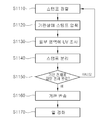
도 2는 도 1에 도시된 와이어 그리드 편광자 제조 시스템에 따른 와이어 그리드 편광자 제조 공정 흐름도이다.FIG. 2 is a flow chart of a wire grid polarizer manufacturing process according to the wire grid polarizer manufacturing system shown in FIG. 1.
도 3a 내지 도 3f는 도 1에 도시된 와이어 그리드 편광자 제조 시스템에 따른 와이어 그리드 편광자 제조 공정 단면도이다. 3A to 3F are cross-sectional views of a wire grid polarizer manufacturing process according to the wire grid polarizer manufacturing system shown in FIG. 1.
도 4는 본 발명의 일 실시예에 따른 와이어 그리드 편광자 제조 시스템의 스탬핑 유닛 및 경화 유닛의 개략 구성도이다. 4 is a schematic structural diagram of a stamping unit and a curing unit of a wire grid polarizer manufacturing system according to an embodiment of the present invention.
도 5는 도 4에 도시된 와이어 그리드 편광자 제조 시스템에 따른 와이어 그리드 편광자 제조 공정 흐름도이다. FIG. 5 is a flow chart of a wire grid polarizer manufacturing process according to the wire grid polarizer manufacturing system shown in FIG. 4.
도 6a 및 도 6b는 본 발명의 다른 실시예에 따른 와이어 그리드 편광자 제조 시스템의 스탬핑 유닛과 경화 유닛의 개략 구성도 및 블록도이다. 6A and 6B are schematic structural diagrams and block diagrams of a stamping unit and a curing unit of a wire grid polarizer manufacturing system according to another embodiment of the present invention.
도 7은 도 6에 도시된 와이어 그리드 편광자 제조 시스템에 따른 와이어 그리드 편광자 제조 공정 흐름도이다. FIG. 7 is a flowchart of a wire grid polarizer manufacturing process according to the wire grid polarizer manufacturing system shown in FIG. 6.
도 8은 본 발명의 또 다른 실시예에 따른 와이어 그리드 편광자 제조 시스템 의 스탬핑 유닛 및 경화 유닛의 개략 구성도이다. 8 is a schematic structural diagram of a stamping unit and a curing unit of a wire grid polarizer manufacturing system according to another embodiment of the present invention.
도 9는 도 8에 도시된 와이어 그리드 편광자 제조 시스템에 따른 와이어 그리드 편광자 제조 공정 흐름도이다. FIG. 9 is a flow chart of a wire grid polarizer manufacturing process according to the wire grid polarizer manufacturing system shown in FIG. 8.
도 10은 본 발명의 또 다른 실시예에 따른 와이어 그리드 편광자 제조 시스템의 스탬핑 유닛 및 경화 유닛의 개략 구성도이다. 10 is a schematic structural diagram of a stamping unit and a curing unit of a wire grid polarizer manufacturing system according to another embodiment of the present invention.
도 11은 도 10에 도시된 와이어 그리드 편광자 제조 시스템에 따른 와이어 그리드 편광자 제조 공정 흐름도이다. FIG. 11 is a flowchart of a wire grid polarizer manufacturing process according to the wire grid polarizer manufacturing system shown in FIG. 10.
도 12는 본 발명에 따른 스탬프의 개략적인 단면도이다.12 is a schematic cross-sectional view of a stamp according to the present invention.
도 13은 단위 스탬프가 베이스 플레이트에 부착되는 원리를 도시한 도이다.13 is a view showing the principle that the unit stamp is attached to the base plate.
도 14는 본 발명에 따른 스탬프의 변형예의 개략적인 단면도이다.14 is a schematic cross-sectional view of a modification of the stamp according to the present invention.
도 15a 내지 도 15d는 단위 스탬프의 제조 공정 단면도이다.15A to 15D are cross-sectional views of the manufacturing process of the unit stamp.
도 16은 본 발명에 따른 와이어 그리드 편광자 제조 시스템의 스탬핑 유닛의 개략 구성도이다.16 is a schematic structural diagram of a stamping unit of the wire grid polarizer manufacturing system according to the present invention.
*도면의 주요 부분에 대한 부호의 설명** Description of the symbols for the main parts of the drawings
100; 로딩 유닛 200; 세정 유닛100; Loading
300; 증착 유닛 400; 코팅 유닛300;
500; 스탬핑 유닛 510; 스탬핑 챔버500;
520; 기판 지지부 530; 스탬프520; A
540; 가압부 550; 스탬프 보관 챔버540;
560; UV 광원 570; UV 광 차단부560;
600; 경화 유닛 610; 경화 챔버600; Curing
620; 기판 지지부 630; 경화 소스부620; A
700; 에칭 유닛 800; 애싱 유닛700;
900; 언로딩 유닛 1000; 반송 유닛900;
본 발명은 와이어 그리드 편광자 제조 시스템 및 제조 방법에 관한 것으로, 보다 상세하게는 나노 임프린트 리소그라피(Nano Imprint Lithography;NIL) 공정을 대형 기판에 적용하며, 제조 공정 시간을 단축하고, 가공 정밀도를 향상시키기 위한 와이어 그리드 편광자 제조 시스템 및 제조 방법에 관한 것이다.The present invention relates to a wire grid polarizer manufacturing system and a manufacturing method, and more particularly, to apply a nano imprint lithography (NIL) process to a large substrate, to shorten the manufacturing process time, to improve the processing precision The present invention relates to a wire grid polarizer manufacturing system and a manufacturing method.
와이어 그리드 편광자(Wire Grid Polarizer)는 기본 원리가 인간이 인지하고 있는 가시 광선 영역인 R, G, B 파장 크기 보다 작은 금속 재료 선폭 및 스페이싱(Spacing)을 갖는 스트라이프 형태의 와이어 그리드 패턴이 유리 기판 또는 편광자 형성용 필름 상에 박막 가공 방법을 이용하여 형성된 구조로 되어 있다. 가시광선의 최저 광학 파장인 블루 영역 보다 작은 (50nm ∼ 200nm) 정도의 선폭 및 간격을 갖는 금속 와이어 그리드 패턴에 광이 입사되면, 광학의 일반적인 특성상 진행방향에 대하여 수평 및 수직 방향으로 진동하면서 진행하는 특성이 있기 때문에, 금속 와이어 그리드 패턴의 스페이싱이 존재하는 부위와 평행하게 입사되는 광만이 금속 와이어 그리드 패턴을 통과하게 되어, 와이어 그리드 편광자는 편광 기능을 수행하게 된다.Wire Grid Polarizer is a stripe-shaped wire grid pattern with a metal material line width and spacing less than R, G, B wavelength size, which is the basic principle of human visible light. It has a structure formed on the film for polarizer formation using the thin film processing method. When light is incident on a metal wire grid pattern having a line width and a spacing smaller than the blue region, which is the lowest optical wavelength of visible light, (50 nm to 200 nm), the light propagates while vibrating in the horizontal and vertical directions with respect to the propagation direction. Because of this, only light incident in parallel with the portion where the spacing of the metal wire grid pattern exists passes through the metal wire grid pattern, so that the wire grid polarizer performs a polarizing function.
이와 같은 편광상의 장점으로 인하여, 와이어 그리드 편광자가 액정표시장치에 적용될 경우 액정표시장치의 슬림화, 제조 공정의 단순화 및 제조 비용의 절감 등의 효과를 가져올 수 있다. 그러나, 와이어 그리드 편광자는 근본적으로 (50∼200nm) 정도의 나노 스케일의 금속 박막의 패터닝 공정으로 이루어지기 때문에, 와이어 그리드 편광자를 액정표시장치에 적용할 정도로 대형화하는데 어려운 점이 있었으며, 제조 공정 시간의 증가로 인하여 경제성을 확보할 수 없다는 문제점이 있었다. Due to such polarization advantages, when the wire grid polarizer is applied to the liquid crystal display device, the liquid crystal display device may have an effect of slimming, simplifying the manufacturing process, and reducing the manufacturing cost. However, since the wire grid polarizer is essentially a patterning process of a nano-scale metal thin film of about (50 to 200 nm), it has been difficult to increase the size of the wire grid polarizer so that it can be applied to a liquid crystal display device. There was a problem that can not secure economic feasibility.
특히, 나노 임프린트 리소그라피 공정으로 와이어 그리드 편광자를 제조하는데 있어서 대형화 및 제조 공정 시간을 결정짓는 가장 주요한 공정은 소정 패턴이 형성된 스탬프를 기판 상에 전사시키는 스탬핑 공정인데, 종래 기술에 따르면 압착, 가압 및 경화 공정 등 여러 가지 공정을 동일 챔버 내에서 수행했기 때문에, 다음 공정 진행을 위한 대기 시간의 증가로 인하여, 제조 공정 시간이 길어지는 문제점이 있다. In particular, in the manufacture of a wire grid polarizer by a nanoimprint lithography process, the most important step for determining the size and manufacturing process time is a stamping process for transferring a stamp having a predetermined pattern onto a substrate. Since various processes such as processes are performed in the same chamber, there is a problem in that the manufacturing process time becomes longer due to an increase in waiting time for the next process.
또한, 스탬프의 크기가 공정적으로 액정표시장치의 패널 크기에 대응되지 않기 때문에 양산성이 떨어지는 문제점이 있다. 이를 극복하기 위하여, 대형 기판에 소형 스탬프를 연속적으로 반복하여 스탬핑하는 방법도 사용되고 있으나, 이러한 방식은 스탬핑하는데 오랜 시간이 소요되는 동시에, 정렬 오차가 발생되어 와이어 그리드 편광자의 정밀도가 현저히 저하되는 문제점이 발생하게 된다. In addition, since the size of the stamp does not fairly correspond to the size of the panel of the liquid crystal display device, there is a problem in that mass productivity is poor. In order to overcome this problem, a method of repeatedly stamping a small stamp on a large substrate is also used. However, this method takes a long time to stamp, and at the same time, an alignment error occurs, which significantly reduces the precision of the wire grid polarizer. Will occur.
본 발명은 상술한 종래의 문제점을 극복하기 위한 것으로서, 본 발명이 이루고자 하는 기술적 과제는 와이어 그리드 편광자의 대형화, 제조 공정 시간의 단축 및 가공 정밀도 향상이 가능한 와이어 그리드 편광자 제조 시스템 및 제조 방법을 제공하기 위한 것이다.The present invention is to overcome the above-mentioned conventional problems, the technical problem to be achieved by the present invention is to provide a wire grid polarizer manufacturing system and manufacturing method capable of increasing the size of the wire grid polarizer, shortening the manufacturing process time and improving processing accuracy It is for.
상기 본 발명의 목적을 달성하기 위한 본 발명의 일 측면에 따르면, 기판 상에 금속 박막층을 형성하기 위한 증착 유닛; 상기 금속 박막층 상에 포토 레지스트를 도포 및 상기 포토 레지스트를 베이크하기 위한 코팅 유닛; 패턴이 형성된 스탬프를 포함하며, 상기 스탬프의 패턴을 상기 포토 레지스트에 전사시키기 위하여, 상기 스탬프를 상기 포토 레지스트 상에 압착하는 스탬핑 유닛; 및 상기 포토 레지스트를 경화시키기 위한 경화 유닛을 포함하는 것을 특징으로 하는 와이어 그리드 편광자 제조 시스템이 제공된다.According to an aspect of the present invention for achieving the object of the present invention, a deposition unit for forming a metal thin film layer on a substrate; A coating unit for applying photoresist on the metal thin film layer and baking the photoresist; A stamping unit including a stamp having a pattern formed thereon, the stamping unit compressing the stamp onto the photoresist to transfer the pattern of the stamp to the photoresist; And a curing unit for curing the photoresist.
상기 와이어 그리드 편광자 제조 시스템은 상기 금속 박막층을 식각하기 위한 에칭 유닛; 및 상기 포토 레지스트를 제거하기 위한 애싱 유닛을 더 포함한다.The wire grid polarizer manufacturing system includes an etching unit for etching the metal thin film layer; And an ashing unit for removing the photoresist.
상기 와이어 그리드 편광자 제조 시스템은 상기 기판을 반입하기 위한 로딩 유닛; 상기 기판을 세정하기 위한 세정 유닛; 상기 기판을 반출하기 위한 언로딩 유닛; 및 상기 기판을 반송하기 위한 반송 유닛을 더 포함한다.The wire grid polarizer manufacturing system includes a loading unit for importing the substrate; A cleaning unit for cleaning the substrate; An unloading unit for carrying out the substrate; And a conveying unit for conveying the substrate.
상기 유닛들은 로딩 유닛, 세정 유닛, 증착 유닛, 코팅 유닛, 스탬핑 유닛, 경화 유닛, 에칭 유닛, 애싱 유닛 및 언로딩 유닛의 순서로 인라인으로 설치되며, 상기 반송 유닛은 상기 각 유닛 사이에 설치된다.The units are installed inline in the order of a loading unit, a cleaning unit, a deposition unit, a coating unit, a stamping unit, a curing unit, an etching unit, an ashing unit and an unloading unit, and the conveying unit is installed between the units.
상기 스탬핑 유닛은 스탬핑 챔버; 상기 스탬핑 챔버 내에 배치되며, 상기 기판을 지지하기 위한 제1 기판 지지부; 상기 스탬프를 상기 기판 상에 압착하기 위하여, 상기 스탬프에 압력을 인가하는 가압부를 더 포함한다.The stamping unit comprises a stamping chamber; A first substrate support disposed in the stamping chamber, the first substrate support supporting the substrate; In order to squeeze the stamp on the substrate, it further comprises a pressing unit for applying pressure to the stamp.
상기 스탬프는 베이스 플레이트; 상기 베이스 플레이트의 일 면 상에 상호 교대로 배치되며, 서로 극성이 다른 제1 자석과 제2 자석; 및 상기 베이스 플레이트의 일 면 상에 부착되는 복수의 단위 스탬프를 포함한다.The stamp is a base plate; First and second magnets disposed alternately on one surface of the base plate and different in polarity from each other; And a plurality of unit stamps attached on one surface of the base plate.
상기 단위 스탬프는 단위 스탬프 기판; 및 상기 단위 스탬프 기판의 일 면 상에 형성된 일 방향으로 형성된 미세 패턴을 포함한다.The unit stamp is a unit stamp substrate; And a fine pattern formed in one direction formed on one surface of the unit stamp substrate.
상기 단위 스탬프 기판의 타 면 상에 형성된 금속 도전층을 더 포함한다.Further comprising a metal conductive layer formed on the other surface of the unit stamp substrate.
상기 단위 스탬프 기판은 실리콘 웨이퍼 또는 수정(Quartz) 웨이퍼로 이루어진다.The unit stamp substrate is made of a silicon wafer or a quartz wafer.
상기 가압부는 가압 챔버; 및 상기 가압 챔버 내에 기체를 주입하여 기체 압력을 인가하기 위한 기체 압력 인가부를 포함한다.The pressurizing portion is a pressurizing chamber; And a gas pressure applying unit for applying a gas pressure by injecting gas into the pressurization chamber.
상기 가압 챔버 내에 인가되는 기체 압력의 균일도를 유지하기 위한 기체 압력 보정부를 더 포함한다.The apparatus further includes a gas pressure correction unit for maintaining a uniformity of the gas pressure applied in the pressurization chamber.
상기 기체 압력 인가부는 상기 가압 챔버 외부에 설치되어, 상기 가압 챔버에 주입되는 기체를 제공하는 기체 공급원; 및 상기 가압 챔버의 벽에 형성된 기체 주입홀을 포함한다.The gas pressure applying unit is provided outside the pressurization chamber, the gas supply source for providing a gas injected into the pressurization chamber; And a gas injection hole formed in a wall of the pressurization chamber.
상기 기체 압력 보정부는 복수의 스프링 부재를 포함하며, 상기 복수의 스프링 부재는 상기 가압 챔버의 내부에 설치된다.The gas pressure corrector includes a plurality of spring members, and the plurality of spring members are installed in the pressure chamber.
상기 와이어 그리드 편광자 제조 시스템은 예비 스탬프를 보관하기 위한 스탬프 보관 챔버를 더 포함한다.The wire grid polarizer manufacturing system further includes a stamp storage chamber for storing the preliminary stamp.
상기 경화 유닛은 경화 챔버; 상기 경화 챔버 내에 배치되며, 상기 기판을 지지하기 위한 제2 기판 지지부; 및 상기 포토 레지스트를 경화시키기 위한 경화 소스부를 포함한다.The curing unit comprises a curing chamber; A second substrate support disposed in the curing chamber, for supporting the substrate; And a curing source portion for curing the photoresist.
상기 포토 레지스트는 UV 경화성 포토 레지스트 또는 열 경화성 포토 레지스트이다.The photoresist is a UV curable photoresist or heat curable photoresist.
상기 경화 소스부는 UV 광원 또는 히터를 포함한다.The curing source portion includes a UV light source or a heater.
상기 포토 레지스트는 UV 경화성 포토 레지스트 및 열 경화성 포토 레지스트가 혼합되어 구성된 하이브리드 포토 레지스트를 포함한다.The photoresist includes a hybrid photoresist configured by mixing a UV curable photoresist and a thermosetting photoresist.
상기 스탬핑 유닛은 상기 하이브리드 포토 레지스트 중 UV 경화성 포토 레지스트를 경화시키기 위한 UV 광원을 더 포함하며, 상기 경화 유닛의 경화 소스부는 상기 하이브리드 포토 레지스트 중 열 경화성 포토 레지스트를 경화시키기 위한 히터를 포함한다.The stamping unit further includes a UV light source for curing the UV curable photoresist of the hybrid photoresist, wherein the curing source portion of the curing unit includes a heater for curing the thermosetting photoresist of the hybrid photoresist.
상기 스탬핑 유닛은 상기 UV 광원으로부터 조사되는 UV 광의 일부를 차단하기 위한 UV 광 차단부를 더 포함한다.The stamping unit further includes a UV light blocking unit for blocking a part of the UV light irradiated from the UV light source.
상기 UV 광 차단부는 금속막을 포함한다.The UV light blocking unit includes a metal film.
상기 에칭 유닛은 상기 금속 박막층을 건식 식각하는 것을 특징으로 한다.The etching unit is characterized in that dry etching the metal thin film layer.
한편, 본 발명의 다른 측면에 따르면, 기판을 마련하는 단계; 상기 기판 상에 금속 박막층을 형성하는 단계; 상기 금속 박막층 상에 포토 레지스트를 도포하 는 단계; 상기 포토 레지스트가 도포된 기판을 베이크하는 단계; 패턴이 형성된 스탬프를 마련하는 단계; 상기 스탬프의 패턴을 상기 포토 레지스트에 전사시키기 위하여, 상기 스탬프를 상기 기판의 포토 레지스트 상에 정렬 및 압착시키는 단계; 상기 포토 레지스트를 경화시키는 단계; 상기 스탬프를 상기 기판으로부터 분리시키는 단계; 및 상기 기판의 금속 박막층을 식각하는 단계를 포함하는 것을 특징으로 하는 와이어 그리드 편광자 제조 방법이 제공된다.On the other hand, according to another aspect of the invention, preparing a substrate; Forming a metal thin film layer on the substrate; Applying a photoresist on the metal thin film layer; Baking the substrate on which the photoresist is applied; Providing a patterned stamp; Aligning and compressing the stamp onto the photoresist of the substrate to transfer the pattern of the stamp to the photoresist; Curing the photoresist; Separating the stamp from the substrate; And it provides a wire grid polarizer manufacturing method comprising the step of etching the metal thin film layer of the substrate.
본 발명의 또 다른 측면에 따르면, 기판을 마련하는 단계; 상기 기판 상에 금속 박막층을 형성하는 단계; 상기 금속 박막층 상에 포토 레지스트를 도포하는 단계; 상기 포토 레지스트가 도포된 기판을 베이크하는 단계; 패턴이 형성된 스탬프를 마련하는 단계; 상기 스탬프의 패턴을 상기 포토 레지스트에 전사시키기 위하여, 상기 스탬프를 상기 기판의 포토 레지스트 상에 정렬 및 압착시키는 단계; 상기 포토 레지스트를 1차 경화시키는 단계; 상기 스탬프를 상기 기판으로부터 분리시키는 단계; 상기 포토 레지스트를 2차 경화시키는 단계; 및 상기 기판의 금속 박막층을 식각하는 단계를 포함하는 것을 특징으로 하는 와이어 그리드 편광자 제조 방법이 제공된다. According to still another aspect of the present invention, there is provided a method of manufacturing a semiconductor device, comprising: preparing a substrate; Forming a metal thin film layer on the substrate; Applying a photoresist on the metal thin film layer; Baking the substrate on which the photoresist is applied; Providing a patterned stamp; Aligning and compressing the stamp onto the photoresist of the substrate to transfer the pattern of the stamp to the photoresist; Primary curing the photoresist; Separating the stamp from the substrate; Secondary curing the photoresist; And it provides a wire grid polarizer manufacturing method comprising the step of etching the metal thin film layer of the substrate.
이하, 첨부된 도면을 참조하여 본 발명의 바람직한 실시예에 대해 상세히 설명한다.Hereinafter, with reference to the accompanying drawings will be described in detail a preferred embodiment of the present invention.
도 1은 본 발명에 따른 와이어 그리드 편광자 제조 시스템의 개략적인 블록도이며, 도 2는 도 1에 도시된 와이어 그리드 편광자 제조 시스템에 따른 와이어 그리드 편광자 제조 공정 흐름도이다.1 is a schematic block diagram of a wire grid polarizer manufacturing system according to the present invention, Figure 2 is a flow chart of a wire grid polarizer manufacturing process according to the wire grid polarizer manufacturing system shown in FIG.
도 1을 참조하면, 와이어 그리드 편광자 제조 시스템은 로딩 유닛(100), 세정 유닛(200), 증착 유닛(300), 코팅 유닛(400), 스탬핑 유닛(500), 경화 유닛(600), 에칭 유닛(700), 애싱 유닛(800), 언로딩 유닛(900) 및 반송 유닛(1000)을 포함한다.Referring to FIG. 1, the wire grid polarizer manufacturing system includes a
와이어 그리드 편광자 제조 시스템은 로딩 유닛(100), 세정 유닛(200), 증착 유닛(300), 코팅 유닛(400), 스탬핑 유닛(500), 경화 유닛(600), 에칭 유닛(700), 애싱 유닛(800) 및 언로딩 유닛(900)의 순서로 설치되어, 인라인 시스템으로 구성된다. 이때, 반송 유닛(1000)은 각 유닛 사이에 설치되어, 각 유닛에서 단위 공정이 완료된 기판을 다음 유닛으로 운반하는 역할을 하게 된다. The wire grid polarizer manufacturing system includes a
인라인으로 구성되는 제조 시스템에서 전체 공정 시간에 가장 주요하게 영향을 주는 요소는 각 단위 공정 유닛의 단위 공정 시간(Tact Time)이다. 즉, 각 단위 공정 유닛의 단위 공정 시간을 균일하게 맞추어서, 어느 한 공정을 완료한 후, 다음 공정을 개시하기까지 대기하는 시간을 최소화하는 것이다. 그러나, 종래 기술에 따른 와이어 그리드 편광자 제조 시스템의 경우, 스탬핑 공정 및 경화 공정을 단일 유닛에서 수행하였기 때문에, 다른 유닛과의 단위 공정 시간의 차이가 현저히 발생하여, 전체 제조 공정 시간이 증가하는 문제점이 발생하였다.The most important factor affecting the overall process time in an inline manufacturing system is the Tact Time of each unit processing unit. That is, the unit process time of each unit process unit is made uniform, and the time to wait until starting a next process after completing one process is minimized. However, in the wire grid polarizer manufacturing system according to the prior art, since the stamping process and the hardening process are performed in a single unit, a difference in unit processing time with other units occurs, resulting in an increase in overall manufacturing process time. Occurred.
따라서, 본 발명에 따른 와이어 그리드 편광자 제조 시스템은 스탬핑과 경화 공정을 단일 유닛에서 수행했던 종래 기술과는 달리, 스탬핑 유닛(500)과 경화 유닛(600)을 분리하여 설치한다. 그 결과, 스탬핑 유닛(500)과 경화 유닛(600)에서 소요되는 단위 공정 시간을 줄일 수 있으며, 스탬핑 유닛(500)과 경화 유닛(600)의 단위 공정 시간을 다른 단위 유닛들의 단위 공정 시간과 거의 유사하게 조절할 수 있게 되어 대기 시간을 최소화할 수 있게 된다.Therefore, the wire grid polarizer manufacturing system according to the present invention, unlike the prior art that the stamping and curing process was performed in a single unit, separately install the
도 1 및 도 2를 참조하여, 와이어 그리드 편광자 제조 시스템의 각 단위 유닛의 역할과 와이어 그리드 편광자의 전체 제조 공정을 살펴보면, 우선 로딩 유닛(100)은 와이어 그리드 편광자를 제조하기 위한 기판(미도시)을 와이어 그리드 제조 시스템 내부로 반입하는 기능을 수행한다(S201). 1 and 2, the role of each unit of the wire grid polarizer manufacturing system and the overall manufacturing process of the wire grid polarizer will be described. First, the
로딩 유닛(100)에 의해 반입된 기판은 반송 유닛(1000)에 의해 세정 유닛(200)으로 이송되며, 세정 유닛(200)은 이송된 기판을 세정하게 된다(S202).The substrate loaded by the
세정된 기판은 반송 유닛(1000)에 의해 증착 유닛(300)으로 이송되며, 증착 유닛(300)은 기판 상에 금속 박막층(미도시)을 형성하게 된다(S203). 이때, 금속 박막층은 예를 들면, 알루미늄(Al) 등과 같은 고반사율 금속 물질을 스퍼터링 방식으로 증착되어 형성된다. 그러나, 금속 박막층의 재료 및 형성 방식은 이에 한정되는 것은 아니며, 다양하게 변형될 수 있다.The cleaned substrate is transferred to the
금속 박막층이 형성된 기판은 반송 유닛(1000)에 의해 코팅 유닛(400)으로 이송되며, 코팅 유닛(400)은 이송된 금속 박막층 상에 나노 스케일급 해상도 대응이 가능한 포토 레지스트를 스핀 코팅 또는 슬릿 코팅 방식으로 도포한다(S204). 그리고 나서, 포토 레지스트를 소정 온도 및 시간을 소프트 베이크(Soft Bake) 처리한다(S205).The substrate on which the metal thin film layer is formed is transferred to the
기판은 반송 유닛(1000)에 의해 스탬핑 유닛(500)으로 이송된다. 스탬핑 유 닛(500)은 패턴이 형성된 스탬프(미도시)를 포함하며, 이와 같은 스탬프에 형성된 패턴을 기판 상에 도포된 포토 레지스트 상에 전사시키기 위하여, 스탬프를 기판 상부에 위치 정렬시킨 후, 포토 레지스트 상에 압착시킨다(S206).The substrate is transferred to the
스탬프가 압착된 기판은 반송 유닛(1000)에 의해 경화 유닛(600)으로 이송되며, 경화 유닛(600)은 포토 레지스트를 경화시킨다(S207). 포토 레지스트가 경화된 후에는 스탬프를 기판으로부터 분리시킨다(S208).The substrate on which the stamp is pressed is transferred to the
스탬프가 분리된 기판은 반송 유닛(1000)에 의해 에칭 유닛(700)으로 이송되며, 에칭 유닛(700)은 스탬프에 의해서 패턴이 형성된 포토 레지스트를 식각 마스크로 하여 금속 박막층을 식각한다(S209). 이때, 식각 공정은 고밀도 RIE(reactive ion etching), PE(plasma etching ), ICP(Inductively Coupled Plasma) 방식 등을 이용하는 건식 식각 방식으로 금속 박막층을 식각한다.The substrate from which the stamp is separated is transferred to the
식각 공정이 완료된 기판은 반송 유닛(1000)에 의해 애싱 유닛(800)으로 이송되며, 애싱 유닛(800)은 식각 마스크로 이용된 포토 레지스트를 제거하여 와이어 그리드 편광자를 완성하게 된다(S210). The substrate on which the etching process is completed is transferred to the
완성된 와이어 그리드 편광자는 반송 유닛(1000)에 의해 언로딩 유닛(900)으로 이송되며, 언로딩 유닛(900)은 완성된 와이어 그리드 편광자를 와이어 그리드 편광자 제조 시스템 외부로 반출하게 된다(S211). The completed wire grid polarizer is transferred to the
도 3a 내지 도 3f는 도 1에 도시된 와이어 그리드 편광자 제조 시스템에 따른 와이어 그리드 편광자 제조 공정 단면도이다. 3A to 3F are cross-sectional views of a wire grid polarizer manufacturing process according to the wire grid polarizer manufacturing system shown in FIG. 1.
도 3a 내지 도 3f를 참조하면, 우선 기판(2100) 상에 금속 박막층(2200)이 형성된다(도 3a). 이때, 금속 박막층(2200)은 상기에서 살펴본 바와 같이, 예를 들면, 알루미늄(Al) 등과 같은 고반사율 금속 물질이 이용되며, 형성 방법은 스퍼터링 방식으로 증착시킨다.3A to 3F, a metal
그 다음에, 금속 박막층(2200) 상에 포토 레지스트(2300)를 스핀 코팅 또는 슬릿 코팅 방식으로 도포한 후, 도포된 포토 레지스트를 소정 온도 및 시간을 소프트 베이크(Soft Bake)한다(도 3b).Next, after the
패턴이 형성된 스탬프(530)를 기판 상부에 위치 정렬시킨 후, 포토 레지스트 상(2300)에 압착시킨다(도 3c). 그리고 나서, 포토 레지스트(2300)를 경화시킨 후, 스탬프(530)를 분리하면, 스탬프에 형성된 패턴이 포토 레지스트에 전사되어, 포토 레지스트에는 스탬프의 패턴과 반대 모양의 패턴이 형성된다(도 3d).The patterned
패턴이 형성된 포토 레지스트(2300)를 식각 마스크로 하여 금속 박막층(2200)을 식각한다(도 3e). 그 다음에, 금속 박막층(2200) 상부에 잔존하는 포토 레지스트(2300)를 제거하면, 기판(2100) 상에는 패턴 예를 들면, 와이어 그리드 패턴(wire grid pattern)을 갖는 금속 박막층(2200)이 형성되어, 와이어 그리드 편광자가 완성된다.The metal
이하의 실시예들에서는 와이어 그리드 편광자 제조 시스템의 스탬핑 유닛(500)과 경화 유닛(600)을 중심으로 설명하며, 나머지 단위 유닛과 단위 공정은 상기에서 설명한 내용과 중복되므로 생략한다.In the following embodiments, the
도 4는 본 발명의 일 실시예에 따른 와이어 그리드 편광자 제조 시스템의 스탬핑 유닛 및 경화 유닛의 개략 구성도이며, 도 5는 도 4에 도시된 와이어 그리드 편광자 제조 시스템에 따른 와이어 그리드 편광자 제조 공정 흐름도이다. 4 is a schematic structural diagram of a stamping unit and a curing unit of the wire grid polarizer manufacturing system according to an embodiment of the present invention, Figure 5 is a flow chart of a wire grid polarizer manufacturing process according to the wire grid polarizer manufacturing system shown in FIG. .
도 4를 참조하면, 스탬핑 유닛(500)은 스탬핑 챔버(510), 제1 기판 지지부(520), 스탬프(530) 및 가압부(540)를 포함하며, 경화 유닛(600)은 경화 챔버(610), 제2 기판 지지부(620) 및 경화 소스부(630)를 포함한다.Referring to FIG. 4, the
스탬핑 유닛(500)의 스탬핑 챔버(510)는 스탬핑 유닛(500)의 다양한 구성요소가 설치될 소정의 공간을 제공한다.The stamping
제1 기판 지지부(520)는 스탬핑 챔버(510) 내에 배치되며, 스탬핑 챔버(510) 내부로 이송된 기판(2000)을 지지하는 역할을 수행한다. 이때, 기판(2000)은 이전 단위 유닛 예를 들면, 세정 유닛, 증착 유닛 및 코팅 유닛에서 수행된 단위 공정들을 통하여, 금속 박막층 및 포토 레지스트가 순차적으로 형성된 기판을 의미한다.The first
스탬프(530)는 소정 선폭 및 간격을 갖는 스트라이프 패턴(미도시)이 일 면상에 형성되며, 이러한 패턴을 기판 상에 도포된 포토 레지스트 상에 전사하는 기능을 수행한다. 스탬프(530)의 구조 및 제조 방법에 대해서는 이하의 도 12 내지 도 15를 참조하여 더욱 상세히 살펴본다. The
가압부(540)는 스탬핑 챔버(510) 상부에 배치되며, 스탬프(530)에 압력을 인가하여, 스탬프(530)를 상하방향으로 이동시켜 기판(2000) 상에 압착하는 기능을 수행한다. 가압부(540)의 구조 및 동작에 대해서는 이하의 도 16을 참조하여 더욱 상세히 살펴본다.The
본 실시예의 경우, 제1 기판 지지부(520)가 스탬핑 챔버(510)의 하부에 배치되고, 가압부(540)가 스탬핑 챔버(510)의 상부에 배치되어, 가압부(540)가 스탬프(530)를 제1 기판 지지부(520)의 방향 즉, 하부 방향으로 이동시켜 기판(2000) 상에 압착하게 되나, 이에 한정되는 것은 아니다. 이와는 달리, 제1 기판 지지부(520)와 가압부(540)의 위치가 서로 바뀌어 설치될 수도 있다. 즉, 가압부(540)를 스탬핑 챔버(510)의 하부에 배치하고, 제1 기판 지지부(520)를 상부에 배치할 수도 있다. 이렇게 설치하게 되면, 스탬핑 공정 진행 중 불순물이 기판 상에 떨어지는 것을 방지할 수 있어, 기판이 불순물에 오염되는 것을 최소화할 수 있게 된다.In the present exemplary embodiment, the
경화 유닛(600)은 경화 챔버(610)와, 경화 챔버(610) 내에 배치되며, 스탬핑 유닛(500)으로부터 이송된 기판(2000)을 지지하기 위한 제2 기판 지지부(620) 및 기판 상의 포토 레지스트를 경화시키기 위한 경화 소스부(630)를 포함한다.The
한편, 스탬핑 유닛(500) 이전에 설치된 코팅 유닛(400, 도 1 참조)에서 기판 상에 도포하는 포토 레지스트로는 예를 들면, 아크릴레이트(Acrylate)계 폴리머를 포함하는 UV 경화성 포토 레지스트 또는 에폭시(Epoxy)계 폴리머를 포함하는 열 경화성 포토 레지스트를 이용할 수 있다. 이에 따라, 경화 소스부(630)는 코팅 유닛에서 이용한 포토 레지스트의 종류에 따라 UV 광원 또는 히터를 이용할 수 있다.Meanwhile, the photoresist applied on the substrate in the coating unit 400 (see FIG. 1) installed before the
도 4 및 도 5를 참조하여, 와이어 그리드 편광자 제조 공정을 살펴보면, 우선 금속 박막층과 포토 레지스트가 순차적으로 형성된 기판(2000)이 스탬핑 유 닛(500)으로 이송되어, 제1 기판 지지부(520) 상에 안착되면, 스탬프(530)를 위치 정렬한다(S510). Referring to FIG. 4 and FIG. 5, referring to a wire grid polarizer manufacturing process, first, a
스탬프(530)가 위치 정렬되면, 가압부(540)를 이용하여 스탬프(530)를 기판(2000) 상에 압착하게 된다(S520).When the
스탬프(530)가 압착된 기판(2000)은 반송 유닛(1000)에 의해 경화 유닛(600)으로 이송된다(S530). The
경화 유닛(600)으로 이송된 기판(2000)은 스탬프(530)가 압착된 상태로 제2 기판 지지부(620) 상에 안착되며, 경화 소스부(630)에서는 UV 광원 또는 열을 조사하여 기판 상에 형성된 포토 레지스트를 경화시킨다(S540). 포토 레지스트의 경화가 완료되면, 스탬프(530)를 분리한다(S550).The
그리고 나서, 분리된 스탬프(530)는 다시 스탬핑 유닛(530)으로 역반송시키며, 기판(2000)은 다음 공정을 진행하기 위하여, 경화 유닛의 다음에 설치된 에칭 유닛(700, 도 1 참조)으로 이송하게 된다. Then, the separated
도 6a 및 도 6b는 본 발명의 다른 실시예에 따른 와이어 그리드 편광자 제조 시스템의 스탬핑 유닛과 경화 유닛의 개략 구성도 및 블록도이며, 도 7은 도 6에 도시된 와이어 그리드 편광자 제조 시스템에 따른 와이어 그리드 편광자 제조 공정 흐름도이다. 도 6a 내지 도 7에 도시된 실시예는 도 4 및 도 5에 도시된 실시예와 비교하여, 복수의 스탬프를 사용한다는 점이 상이하며, 나머지 구성은 거의 유사하므로, 이하에서는 상이한 구성을 위주로 상술한다.6A and 6B are schematic structural diagrams and block diagrams of a stamping unit and a curing unit of a wire grid polarizer manufacturing system according to another embodiment of the present invention, and FIG. 7 is a wire according to the wire grid polarizer manufacturing system shown in FIG. 6. Grid polarizer manufacturing process flow chart. 6A to 7 are different from the embodiments shown in FIGS. 4 and 5 in that a plurality of stamps are used, and since the rest of the configuration is almost similar, the following description will focus on different configurations. .
도 6a 및 도 6b를 참조하면, 스탬핑 유닛(500)은 스탬핑 챔버(510), 제1 기판 지지부(520), 스탬프(530), 가압부(540) 및 스탬프 보관 챔버(550)를 포함하며, 경화 유닛(600)은 경화 챔버(610), 제2 기판 지지부(620) 및 경화 소스부(630)를 포함한다.6A and 6B, the
스탬핑 유닛(500)의 스탬핑 챔버(510)는 스탬핑 유닛(500)의 다양한 구성요소가 설치될 소정의 공간을 제공하며, 제1 기판 지지부(520)는 스탬핑 챔버(510) 내에 배치되며, 스탬핑 챔버(510) 내부로 이송된 기판(2000)을 지지하는 역할을 수행한다. 스탬프(530)는 소정 선폭 및 간격을 갖는 스트라이프 패턴(미도시)이 일 면상에 형성되며, 이러한 패턴을 기판 상에 도포된 포토 레지스트 상에 전사하는 기능을 수행하는데, 본 실시예에서는 스탬프(530)가 복수개 사용된다.The stamping
가압부(540)는 스탬핑 챔버(510) 상부에 배치되며, 스탬프(530)에 압력을 인가하여, 스탬프(530)를 상하방향으로 이동시켜 기판(2000) 상에 압착하는 기능을 수행한다.The
스탬프 보관 챔버(550)는 스탬핑 유닛(500)의 스탬프 챔버(510) 내에 배치되는 스탬프 이외에 별도의 스탬프를 보관하며, 이러한 예비 스탬프를 스탬프 챔버(510)에 제공하는 기능을 수행한다. The
스탬핑 유닛(500)에서 스탬핑 공정이 완료된 기판은 스탬프가 압착된 상태로 경화 유닛(600)으로 이송되기 때문에, 스탬프 챔버(510) 내에는 스탬프가 없게 된다. 그 결과, 다음 기판의 스탬핑 공정을 진행하기 위해서는 경화 유닛(600)의 경화 공정이 완료된 후, 기판으로부터 분리된 스탬프가 스탬프 챔버(510)로 역반송될 때까지 대기해야 한다. 그러나, 본 실시예와 같이, 스탬프 보관 챔버(550)를 추가로 구성하고, 복수개의 스탬프를 사용하게 되면, 경화 유닛(600)에서 경화 공정을 진행하는 도중에 스탬프 보관 챔버(550)에서 예비 스탬프를 스탬프 챔버(510)로 반송하기 때문에, 경화 공정이 완료된 후 스탬프가 역반송될 때까지의 대기 시간을 줄일 수 있게 된다.Since the substrate in which the stamping process is completed in the
도 6a 내지 도 7을 참조하여, 와이어 그리드 편광자 제조 공정을 살펴보면, 우선 금속 박막층과 포토 레지스트가 순차적으로 형성된 기판(2000)이 스탬핑 유닛(500)으로 이송되어, 제1 기판 지지부(520) 상에 안착되면, 스탬프(530)를 위치 정렬한다(S710). 스탬프(530)가 위치 정렬되면, 가압부(540)를 이용하여 스탬프(530)를 기판(2000) 상에 압착하게 된다(S720).Referring to FIGS. 6A to 7, a process of manufacturing a wire grid polarizer may be described. First, a
스탬프(530)가 압착된 기판(2000)은 반송 유닛(1000)에 의해 경화 유닛(600)으로 이송된다(S730). 이와 동시에, 스탬프 보관 챔버(550)에 보관되어 있던 예비 스탬프는 스탬프 챔버(510)로 이송되어, 스탬핑 유닛(500)에서는 다음 기판의 스탬핑 공정을 준비하게 된다.The
경화 유닛(600)으로 이송된 기판(2000)은 스탬프(530)가 압착된 상태로 제2 기판 지지부(620) 상에 안착되며, 경화 소스부(630)에서는 UV 광원 또는 열을 조사하여 기판 상에 형성된 포토 레지스트를 경화시킨다(S540). 포토 레지스트의 경화가 완료되면, 스탬프(530)를 분리한다(S550).The
그리고 나서, 분리된 스탬프(530)는 스탬프 보관 챔버(550)로 반송되어, 스 탬프 보관 챔버(550)에 보관되며, 기판(2000)은 다음 공정을 진행하기 위하여, 경화 유닛의 다음에 설치된 에칭 유닛(700, 도 1 참조)으로 이송하게 된다. Then, the separated
도 8은 본 발명의 또 다른 실시예에 따른 와이어 그리드 편광자 제조 시스템의 스탬핑 유닛 및 경화 유닛의 개략 구성도이며, 도 9는 도 8에 도시된 와이어 그리드 편광자 제조 시스템에 따른 와이어 그리드 편광자 제조 공정 흐름도이다. 8 is a schematic structural diagram of a stamping unit and a curing unit of the wire grid polarizer manufacturing system according to another embodiment of the present invention, Figure 9 is a flow chart of the wire grid polarizer manufacturing process according to the wire grid polarizer manufacturing system shown in FIG. to be.
도 8 및 도 9에 도시된 실시예는 상기 실시예들과 비교하여, 스탬핑 유닛과 경화 유닛에서 각각 경화 공정을 수행하며, 스탬프의 분리 시기가 상이하며, 나머지 구성은 거의 유사하므로, 이하에서는 상이한 구성을 위주로 상술한다.8 and 9 perform the curing process in the stamping unit and the curing unit, respectively, compared to the above embodiments, the separation timing of the stamps are different, and the rest of the configuration is almost similar, different The configuration will be described in detail.
스탬핑 유닛(500)은 스탬핑 챔버(510), 제1 기판 지지부(520), 스탬프(530),가압부(540) 및 UV 광원(560)을 포함하며, 경화 유닛(600)은 경화 챔버(610), 제2 기판 지지부(620) 및 히터(635)를 포함한다.The
한편, 스탬핑 유닛(500) 이전에 설치된 코팅 유닛(400, 도 1 참조)에서 기판 상에 도포하는 포토 레지스트로는 UV 경화성 포토 레지스트 및 열 경화성 포토 레지스트가 혼합되어 구성된 하이브리드 포토 레지스트를 이용할 수 있다. 이때, UV 경화성 포토 레지스트는 예를 들면, 아크릴레이트(Acrylate)계 폴리머를 포함할 수 있으며, 열 경화성 포토 레지스트는 예를 들면, 에폭시(Epoxy)계 폴리머를 포함할 수 있다.Meanwhile, as the photoresist applied on the substrate in the coating unit 400 (see FIG. 1) installed before the
스탬핑 유닛(500)은 하이브리드 포토 레지스트 중 UV 경화성 포토 레지스트를 경화시키기 위하여, UV 광원(560)이 추가적으로 설치된다. 이때, UV 광원(560) 은 스탬핑 챔버(510)의 상부에 배치된 가압부(540)에 설치될 수 있다. 그러나, UV 광원(560)의 설치 위치는 이에 한정되는 것은 아니며, 다양한 위치에 설치 가능하다.The
경화 유닛(600)의 경화 소스부는 하이브리드 포토 레지스트 중 열 경화성 포토 레지스트를 경화시키기 위한 히터(635)로 구성된다. The curing source portion of the
도 8 및 도 9를 참조하여, 와이어 그리드 편광자 제조 공정을 살펴보면, 우선 금속 박막층과 포토 레지스트가 순차적으로 형성된 기판(2000)이 스탬핑 유닛(500)으로 이송되어, 제1 기판 지지부(520) 상에 안착되면, 스탬프(530)를 위치 정렬한다(S910). 이때, 기판(2000) 상에 형성된 포토 레지스트는 상기에서 살펴본 바와 같이, UV 경화성 포토 레지스트 및 열 경화성 포토 레지스트가 혼합되어 구성된 하이브리드 포토 레지스트이다.8 and 9, the wire grid polarizer manufacturing process will be described. First, the
스탬프(530)가 위치 정렬되면, 가압부(540)를 이용하여 스탬프(530)를 기판(2000) 상에 압착하게 된다(S920). 이때, 스탬프(530)의 크기는 기판(2000)의 크기에 상응하는 크기로 형성된 스탬프를 사용하여, 한 번의 압착으로 스탬프의 패턴이 기판 상에 전사되도록 한다. When the
그 다음에, UV 광원(560)을 이용하여 UV 광을 기판의 하이브리드 포토 레지스트 상에 조사하여, 하이브리드 포토 레지스트의 성분 중 UV 경화성 포토 레지스트를 우선적으로 경화시킨다(S930). 그리고 나서, 스탬프(530)를 분리하게 된다(S940). Next, UV light is irradiated onto the hybrid photoresist of the substrate using the UV
스탬프(530)가 분리된 기판(2000)은 반송 유닛(1000)에 의해 경화 유닛(600)으로 이송된다(S950). The
경화 유닛(600)으로 이송된 기판(2000)은 기판 지지부(620) 상에 안착되며,히터(635)에서는 열을 조사하여 기판 상에 형성된 하이브리드 포토 레지스트 중 열 경화성 포토 레지스트를 경화시킨다(S960). 그리고 나서, 기판(2000)은 다음 공정을 진행하기 위하여, 경화 유닛의 다음에 설치된 에칭 유닛(700, 도 1 참조)으로 이송하게 된다. The
이와 같이, 포토 레지스트를 UV 경화성 포토 레지스트와 열 경화성 포토 레지스트를 혼합한 하이브리드 포토 레지스트를 사용하면, 하이브리드 포토 레지스트가 기판 상에 도포되어 있는 상태에서 스탬프를 압착한 후, UV 광을 조사해 주면, 하이브리드 포토 레지스트의 성분 중 UV 경화성 포토 레지스트가 경화하면서, 일정 형상을 유지하게 된다. 이러한 상태에서 스탬프를 하이브리드 포토 레지스트로부터 분리하더라도, UV경화에 의해서 경화된 UV 경화성 포토 레지스트가 스탬프에 의해서 전사된 패턴을 유지하게 된다. 그 다음에, 경화 유닛으로 이송되어, 열 경화 공정을 거쳐 하이브리드 포토 레지스트의 열 경화성 포토 레지스트를 경화시켜, 하이브리드 포토 레지스트를 완전 경화시킨다.As described above, when using a hybrid photoresist in which the photoresist is a mixture of a UV curable photoresist and a thermosetting photoresist, the hybrid photoresist is irradiated with UV light after pressing the stamp while the hybrid photoresist is applied onto the substrate. While the UV curable photoresist is cured among the components of the photoresist, a constant shape is maintained. Even if the stamp is separated from the hybrid photoresist in this state, the UV curable photoresist cured by UV curing maintains the pattern transferred by the stamp. Then, it is transferred to a curing unit to cure the thermosetting photoresist of the hybrid photoresist through a thermal curing step, thereby completely curing the hybrid photoresist.
이와 같이, 스탬핑 유닛과 경화 유닛에서 각각 경화 공정을 수행하는 이중 경화 방식을 적용하게 되면, 단위 공정 시간을 최대한 단축시킬 수 있게 된다.As such, when the dual curing method for performing the curing process in the stamping unit and the curing unit is applied, the unit process time can be shortened as much as possible.
도 10은 본 발명의 또 다른 실시예에 따른 와이어 그리드 편광자 제조 시스 템의 스탬핑 유닛 및 경화 유닛의 개략 구성도이며, 도 11은 도 10에 도시된 와이어 그리드 편광자 제조 시스템에 따른 와이어 그리드 편광자 제조 공정 흐름도이다. 10 is a schematic structural diagram of a stamping unit and a curing unit of the wire grid polarizer manufacturing system according to another embodiment of the present invention, Figure 11 is a wire grid polarizer manufacturing process according to the wire grid polarizer manufacturing system shown in FIG. It is a flow chart.
도 10 및 도 11에 도시된 실시예는 상기 도 8 및 9에 도시된 실시예와 비교하여, 스탬프의 크기가 기판 보다 작다는 점이 상이하며, 나머지 구성은 거의 유사하므로, 이하에서는 상이한 구성을 위주로 상술한다.10 and 11 are different from the embodiment shown in FIGS. 8 and 9 in that the size of the stamp is smaller than that of the substrate, and the rest of the configuration is almost similar. It is detailed.
스탬핑 유닛(500)은 스탬핑 챔버(510), 제1 기판 지지부(520), 스탬프(530),가압부(540), UV 광원(560) 및 UV 광 차단부(570)을 포함하며, 경화 유닛(600)은 경화 챔버(610), 제2 기판 지지부(620) 및 히터(635)를 포함한다.The
스탬핑 유닛(500) 이전에 설치된 코팅 유닛(400, 도 1 참조)에서 기판 상에 도포하는 포토 레지스트로는 UV 경화성 포토 레지스트 및 열 경화성 포토 레지스트가 혼합되어 구성된 하이브리드 포토 레지스트가 이용되며, 스탬핑 유닛(500)은 하이브리드 포토 레지스트 중 UV 경화성 포토 레지스트를 경화시키기 위하여, UV 광원(560)이 설치된다. As a photoresist applied on the substrate in the coating unit 400 (see FIG. 1) installed before the
한편, 본 실시예에서 이용되는 스탬프(530)의 크기는 기판(2000)의 크기 보다 작은 것이 이용된다. 따라서, 스탬프(530)에 형성된 패턴을 기판의 하이브리드 포토 레지스트에 전사하기 위해서는 적어도 2번 이상 스탬프(530)을 기판 상에 압착하는 공정을 반복해야 한다. 이때, 스탬프(530)를 기판의 하이브리드 포토 레지스트 상에 압착한 후, UV 광원(560)을 이용하여 UV 경화를 시킬 때, 스탬프(530)가 커버되지 않은 영역의 하이브리드 포토 레지스트에 UV 광이 조사되지 않도록 할 필 요가 있다. 이를 위하여, UV 광원(560)으로부터 조사되는 UV 광의 일부를 차단하기 위한 UV 광 차단부(570)가 UV 광원(560) 하부에 설치된다. 이때, UV 광 차단부(570)는 크롬 또는 알루미늄 등과 같은 금속물질로 구성된 금속막으로 형성된다.Meanwhile, the size of the
도 10 및 도 11을 참조하여, 와이어 그리드 편광자 제조 공정을 살펴보면, 우선 금속 박막층과 포토 레지스트가 순차적으로 형성된 기판(2000)이 스탬핑 유닛(500)으로 이송되어, 제1 기판 지지부(520) 상에 안착되면, 스탬프(530)를 위치 정렬한다(S1110). 이때, 기판(2000) 상에 형성된 포토 레지스트는 상기에서 살펴본 바와 같이, UV 경화성 포토 레지스트 및 열 경화성 포토 레지스트가 혼합되어 구성된 하이브리드 포토 레지스트이다. 또한, 스탬프(530)는 기판(2000)의 크기 보다 작은 크기로 형성된 스탬프가 사용된다. Referring to FIGS. 10 and 11, a process of manufacturing a wire grid polarizer, first, a
스탬프(530)가 위치 정렬되면, 가압부(540)를 이용하여 스탬프(530)를 기판(2000) 상에 압착하게 된다(S1120). 그 다음에, UV 광원(560)과 UV 광 차단부(570)를 UV 광을 기판의 일부 영역, 즉 스탬프가 압착되어 있는 영역에만 조사하여, 하이브리드 포토 레지스트의 성분 중 UV 경화성 포토 레지스트를 우선적으로 경화시킨다(S1130). 그리고 나서, 스탬프(530)를 분리하게 된다(S1140). When the
그 다음에, 기판 전체 영역 상에 패턴이 전사될 때까지, 상기 공정을 반복적으로 수행한다(S1150).Next, the process is repeatedly performed until the pattern is transferred onto the entire substrate area (S1150).
그리고 나서, 스탬프(530)가 분리된 기판(2000)은 반송 유닛(1000)에 의해 경화 유닛(600)으로 이송된다(S1160). 경화 유닛(600)으로 이송된 기판(2000)은 기 판 지지부(620) 상에 안착되며, 히터(635)에서는 열을 조사하여 기판 상에 형성된 하이브리드 포토 레지스트 중 열 경화성 포토 레지스트를 경화시킨다(S1170). 그리고 나서, 기판(2000)은 다음 공정을 진행하기 위하여, 경화 유닛의 다음에 설치된 에칭 유닛(700, 도 1 참조)으로 이송하게 된다. Then, the
도 12는 본 발명에 따른 스탬프의 개략적인 단면도이며, 도 13은 단위 스탬프가 베이스 플레이트에 부착되는 원리를 도시한 도이고, 도 14는 본 발명에 따른 스탬프의 변형예의 개략적인 단면도이다.12 is a schematic cross-sectional view of a stamp according to the present invention, FIG. 13 is a view showing the principle that the unit stamp is attached to the base plate, Figure 14 is a schematic cross-sectional view of a modification of the stamp according to the present invention.
도 12 내지 도 14를 참조하면, 스탬프(530)는 베이스 플레이트(531), 자석(532), 복수의 단위 스탬프(535)를 포함한다.12 to 14, the
베이스 플레이트(531)의 일 면에는 서로 극성이 다른 제1 자석 즉, N극 자석(532a)과 제2 자석 즉, S극 자석(532b)이 상호 교대로 배치된다.On one surface of the
복수의 단위 스탬프(535)는 자석(532)이 배치된 베이스 플레이트 상에 부착되며, 이때 각 단위 스탬프(535)에는 미세 패턴(미도시)이 형성된다.A plurality of
도 13을 참조하여, 단위 스탬프(535)가 베이스 플레이트(531)에 부착되는 원리를 살펴보면, 베이스 플레이트(531)의 동일 평면상에는 N극 자석(532a)과 S극 자석(532b)이 상호 교대로 배치되어 있다. 이러한 구조에서 자속(Magnetic Flux)은 N극에서 S극으로 작용하게 되며, 자석 이론인 로렌츠 법칙에 의하면, 자속 방향과 수직 방향, 즉 베이스 플레이트(531)에 대하여 하부에서 상부 방향(화살표 방향)으로 자기 부착력이 발생하게 된다. 이러한 원리로 자기 부착력이 발생되면, 베이스 플레이트(531) 하부에 금속 종류의 물질이 존재하는 경우, 금속 종류의 물질은 베이스 플레이트에 자기적으로 부착된다.Referring to FIG. 13, when the
단위 스탬프(535)의 기판으로는 실리콘 웨이퍼(Si Wafer) 또는 수정 웨이퍼(Quarts Wafer)가 사용될 수 있다. 실리콘 웨이퍼로 형성된 단위 스탬프(535)는 실리콘 웨이퍼 자체가 도전체이기 때문에, 도 12에 도시된 바와 같이 별도의 금속 도전층을 코팅하지 않더라도, 베이스 플레이트(531)에 부착된다. As the substrate of the
그러나, 단위 스탬프(535)의 기판으로 수정 웨이퍼를 사용한 경우에는, 수정 웨이퍼 자체가 전기적으로 절연 재료이기 때문에, 단위 스탬프(535)의 부착면 상에 별도의 금속 도전층(538)를 형성한다(도 14 참조). 한편, 실리콘 웨이퍼를 사용한 경우에도 부착력을 보다 강화시키기 위하여 금속 도전층(538)을 형성할 수도 있다.However, when the quartz wafer is used as the substrate of the
이와 같이, 자석을 이용한 자기 부착력에 의해서 단위 스탬프를 부착하여 대형 스탬프를 제작하게 되면, 고단위 청정실의 대기중이나, 진공 챔버 내에서 동시에 적용할 수 있는 방식이다. 특히, 진공중에서는 기존의 에어 흡입방식이 적용 불가능하지만, 자기 부착력에 의한 부착 방식은 진공 분위기와 관계없이 적용이 가능하고, 부착력의 강도가 우수하므로 장기간의 사용으로 인한 변형이 적다는 장점이 있다.As described above, when a large stamp is manufactured by attaching a unit stamp by a magnetic adhesion force using a magnet, it is a system that can be applied simultaneously in the atmosphere of a high unit clean room or in a vacuum chamber. In particular, the conventional air suction method is not applicable in vacuum, but the self-adhesive attachment method is applicable regardless of the vacuum atmosphere, and the strength of the adhesion force is excellent, so that there is little deformation due to long-term use. .
도 15a 내지 도 15d는 단위 스탬프의 제조 공정 단면도이다.15A to 15D are cross-sectional views of the manufacturing process of the unit stamp.
도 15a 내지 도 15d를 참조하면, 우선 원형의 실리콘 웨이퍼 또는 수정 웨이퍼로 이루어진 단위 스탬프 기판(536)의 일 면 상에 일 방향으로 미세 패턴 즉, 와 이어 그리드 패턴(537)이 형성된다(도 15a).15A to 15D, first, a fine pattern, that is, a
그 다음에, 와이어 그리드 패턴(537)이 형성된 단위 스탬프 기판(536)의 전면에 보호층(539)을 형성한다(도 15b). 이때, 보호층(539)은 포토 레지스트 또는 가용성 폴리머로 구성된 유기 물질층을 도포한 후, 유기 물질층을 베이크하여 형성한다.Next, a
그리고 나서, 와이어 그리드 패턴(537)과 보호층(539)이 형성된 단위 스탬프 기판(536)을 장방형 또는 정방형의 형태로 절단한다(도 15c). 이때, 절단은 다이아몬드 휠 또는 레이저를 이용하여 절단할 수 있다. Then, the
절단이 완료된 후에는 보호층(539)을 제거하여, 단위 스탬프(535)를 완성하게 된다(도 15d). After the cutting is completed, the
이와 같이, 보호층을 형성한 후, 절단 공정을 수행하고, 절단 공정을 완료한 후에 보호층을 제거하게 되면, 절단 공정 시 발생할 수 있는 오염 및 파손을 방지할 수 있게 된다.As such, when the protective layer is formed and then the cutting process is performed and the protective layer is removed after the cutting process is completed, contamination and damage that may occur during the cutting process may be prevented.
도 16은 본 발명에 따른 와이어 그리드 편광자 제조 시스템의 스탬핑 유닛의 개략 구성도이다. 도 16을 참조하여, 스탬핑 유닛(500)의 가압부(540)를 보다 상세히 살펴본다.16 is a schematic structural diagram of a stamping unit of the wire grid polarizer manufacturing system according to the present invention. Referring to FIG. 16, the
스탬핑 유닛(500)의 가압부(540)는 가압 챔버(541)와, 가압 챔버(541) 내에 기체를 주입하여 기체 압력을 인가하기 위한 기체 압력 인가부 및 가압 챔버(541) 내에 인가되는 기체 압력의 균일도를 유지하기 위한 기체 압력 보정부(545)를 포함 하여 구성된다.The pressurizing
기체 압력 인가부는 가압 챔버(541) 외부에 설치되어, 가압 챔버에 주입되는 기체를 제공하는 기체 공급원(미도시)과 가압 챔버(541)의 벽에 형성된 기체 주입홀(543)을 포함하여 구성된다.The gas pressure applying unit is provided outside the
또한, 기체 압력 보정부(545)는 복수의 스프링 부재로 구성되며, 각 스프링 부재는 가압 챔버(541)의 내부에 대칭적인 위치에 설치된다. In addition, the gas
가압 챔버(541) 벽에 형성되어 있는 기체 주입홀(543)을 통하여 기체가 가압 챔버 내부에 주입될 때, 기체의 위치에 따라 국부적으로 스탬프에 압력이 전달되어 균일화되기 전이나 또는 스탬프의 베이스 플레이트의 가공상의 불균일도로 인하여 기체 압력의 전달이 일시적으로 평행을 이루지 못하는 경우가 있을 수 있다.When gas is injected into the pressurizing chamber through the
이러한 경우 기체 압력이 불균일하게 전달되어 특정 방향으로 편중되어 스탬프가 압축시 변위적으로 평형을 손실하더라도, 스프링 부재로 구성된 기체 압력 보정부(545)는 불균형 압력에 의한 압축 변위 편차를 흡수하여 전체적인 가압력의 평형을 즉시 회복하게 하여 가압력의 평형을 이루게 한다. In this case, even if the gas pressure is unevenly transmitted and biased in a specific direction, so that the stamp loses the displacement equilibrium during compression, the
또한, 기체 압력 인가부에서는 가압 챔버(541)에 기체를 순간적으로 주입할 수도 있으며, 이와는 달리 일정시간에 따라 기체를 분할하여 주입하여 가압력을 여러 단계에 걸쳐 제공할 수도 있다. In addition, the gas pressure applying unit may instantaneously inject gas into the
한편, 스탬핑 유닛(500)의 스탬핑 챔버(510)의 측벽에는 챔버를 개폐하기 위한 개폐구(515)가 설치될 수도 있다.On the other hand, the side wall of the stamping
이상에서 설명한 것은 본 발명에 따른 와이어 그리드 편광자 제조 시스템 및 제조 방법의 예시적인 실시예에 불과한 것으로서, 본 발명은 상기한 실시예에 한정되지 않고, 이하의 특허청구범위에서 청구하는 바와 같이, 본 발명의 요지를 벗어남이 없이 당해 발명이 속하는 분야에서 통상의 지식을 가진 자라면 누구든지 다양한 변경 실시가 가능한 범위까지 본 발명의 기술적 정신이 있다고 할 것이다.What has been described above is merely an exemplary embodiment of the wire grid polarizer manufacturing system and manufacturing method according to the present invention, and the present invention is not limited to the above-described embodiment, as claimed in the following claims, the present invention Without departing from the gist of the present invention, those skilled in the art to which the present invention pertains to the technical spirit of the present invention to the extent that various modifications can be made.
전술한 바와 같이 본 발명에 따르면, 와이어 그리드 편광자 제조 시스템의 각 유닛을 인라인으로 설치함으로써, 와이어 그리드 편광자의 제조 공정 시간을 크게 단축할 수 있게 된다. As described above, according to the present invention, by providing each unit of the wire grid polarizer manufacturing system inline, it is possible to greatly shorten the manufacturing process time of the wire grid polarizer.
또한, 복수의 단위 스탬프를 정전력을 이용하여 베이스 플레이트에 부착시켜, 스탬프를 대형화함에 따라, 와이어 그리드 편광자의 대형화가 가능하게 되며, 가공 정밀도 역시 개선된다.In addition, by attaching a plurality of unit stamps to the base plate using electrostatic force to increase the size of the stamp, the size of the wire grid polarizer can be increased, and the machining precision is also improved.
Claims (37)
Priority Applications (6)
| Application Number | Priority Date | Filing Date | Title |
|---|---|---|---|
| KR1020060076959A KR20080015536A (en) | 2006-08-16 | 2006-08-16 | System and method for manufacturing wire grid polarizer |
| JP2006317914A JP2008046580A (en) | 2006-08-16 | 2006-11-27 | System and method for manufacturing wire grid polarizer |
| US11/648,092 US20080041816A1 (en) | 2006-08-16 | 2006-12-29 | Systems and methods for manufacturing wire grid polarizers |
| CNA2007100081174A CN101126894A (en) | 2006-08-16 | 2007-01-26 | Systems and methods for manufacturing wire grid polarizers |
| TW096114603A TW200811487A (en) | 2006-08-16 | 2007-04-25 | Systems and methods for manufacturing wire grid polarizers |
| EP07016076A EP1914571A3 (en) | 2006-08-16 | 2007-08-16 | System and methods for manufacturing wire grid polarizers |
Applications Claiming Priority (1)
| Application Number | Priority Date | Filing Date | Title |
|---|---|---|---|
| KR1020060076959A KR20080015536A (en) | 2006-08-16 | 2006-08-16 | System and method for manufacturing wire grid polarizer |
Publications (1)
| Publication Number | Publication Date |
|---|---|
| KR20080015536A true KR20080015536A (en) | 2008-02-20 |
Family
ID=38962156
Family Applications (1)
| Application Number | Title | Priority Date | Filing Date |
|---|---|---|---|
| KR1020060076959A KR20080015536A (en) | 2006-08-16 | 2006-08-16 | System and method for manufacturing wire grid polarizer |
Country Status (6)
| Country | Link |
|---|---|
| US (1) | US20080041816A1 (en) |
| EP (1) | EP1914571A3 (en) |
| JP (1) | JP2008046580A (en) |
| KR (1) | KR20080015536A (en) |
| CN (1) | CN101126894A (en) |
| TW (1) | TW200811487A (en) |
Cited By (1)
| Publication number | Priority date | Publication date | Assignee | Title |
|---|---|---|---|---|
| KR20190098405A (en) * | 2018-02-14 | 2019-08-22 | 한국기계연구원 | Imprint apparatus using instantaneous heating and liquid transfer, the method |
Families Citing this family (20)
| Publication number | Priority date | Publication date | Assignee | Title |
|---|---|---|---|---|
| TWI481496B (en) * | 2007-12-19 | 2015-04-21 | Heptagon Micro Optics Pte Ltd | Manufacturing optical elements |
| JP5077764B2 (en) | 2008-04-22 | 2012-11-21 | 富士電機株式会社 | Imprint method and apparatus |
| JP5370806B2 (en) * | 2008-04-22 | 2013-12-18 | 富士電機株式会社 | Imprint method and apparatus |
| JP5279397B2 (en) * | 2008-08-06 | 2013-09-04 | キヤノン株式会社 | Imprint apparatus, imprint method, and device manufacturing method |
| JP5149244B2 (en) * | 2009-06-19 | 2013-02-20 | 東京エレクトロン株式会社 | IMPRINT SYSTEM, IMPRINT METHOD, PROGRAM, AND COMPUTER STORAGE MEDIUM |
| CN102044476B (en) * | 2009-10-13 | 2013-06-19 | 中芯国际集成电路制造(上海)有限公司 | Forming method of metal pattern |
| KR20120075877A (en) * | 2010-12-29 | 2012-07-09 | 삼성전자주식회사 | Liquid crystal display panel and apparautus thereof |
| JP2013020182A (en) * | 2011-07-13 | 2013-01-31 | Asahi Kasei E-Materials Corp | Wire grid polarizing plate and method for manufacturing wire grid polarizing plate |
| US20130043956A1 (en) * | 2011-08-15 | 2013-02-21 | Honeywell International Inc. | Systems and methods for a nanofabricated optical circular polarizer |
| KR20140030382A (en) | 2012-08-27 | 2014-03-12 | 삼성디스플레이 주식회사 | Liquid crystal display and fabrication method of the same |
| CN104058362B (en) * | 2013-03-21 | 2017-06-27 | 无锡华润上华半导体有限公司 | The processing method of microelectromechanical systems |
| KR102056902B1 (en) | 2013-05-29 | 2019-12-18 | 삼성전자주식회사 | Wire grid polarizer and liquid crystal display panel and liquid crystal display device having the same |
| KR102089661B1 (en) | 2013-08-27 | 2020-03-17 | 삼성전자주식회사 | Wire grid polarizer and liquid crystal display panel and liquid crystal display device having the same |
| KR101729683B1 (en) | 2015-09-16 | 2017-04-25 | 한국기계연구원 | Manufacturing method of wire grid polarizer |
| CN108351604B (en) | 2016-01-27 | 2020-10-30 | 株式会社Lg化学 | Film mask, method for manufacturing the same, pattern forming method using the film mask, and pattern formed by the film mask |
| EP3410213B1 (en) | 2016-01-27 | 2021-05-26 | LG Chem, Ltd. | Film mask, method for manufacturing same, and method for forming pattern using film mask |
| EP3410214A4 (en) | 2016-01-27 | 2019-01-23 | LG Chem, Ltd. | Film mask, method for manufacturing same, and method for forming pattern using film mask and pattern formed thereby |
| WO2019065098A1 (en) * | 2017-09-27 | 2019-04-04 | 日本電気硝子株式会社 | Glass sheet provided with optical film, and method for manufacturing same |
| CN109270620B (en) | 2018-11-16 | 2022-07-19 | 京东方科技集团股份有限公司 | Manufacturing method of metal wire grid polarizer and display panel |
| CN109445012A (en) * | 2018-12-20 | 2019-03-08 | 深圳市华星光电半导体显示技术有限公司 | Wire grid type polaroid production method and transparent display |
Family Cites Families (10)
| Publication number | Priority date | Publication date | Assignee | Title |
|---|---|---|---|---|
| JP3152257B2 (en) * | 1992-08-10 | 2001-04-03 | 株式会社タツノ・メカトロニクス | Refueling device |
| US7218465B1 (en) * | 2002-06-28 | 2007-05-15 | Seagate Technology Llc | Magnetic media patterning via contact printing utilizing stamper having magnetic pattern formed in non-magnetic substrate |
| KR100484088B1 (en) * | 2002-12-06 | 2005-04-20 | 삼성전자주식회사 | Die attach and cure in line apparatus for multi chip package |
| WO2004092085A2 (en) * | 2003-04-14 | 2004-10-28 | National Graphics, Inc. | Lenticular images formed on selected images portions |
| JP4295592B2 (en) * | 2003-09-30 | 2009-07-15 | 大日本印刷株式会社 | Production method of duplicate plate |
| JP2005153091A (en) * | 2003-11-27 | 2005-06-16 | Hitachi Ltd | Transfer method and transfer device |
| KR100624414B1 (en) * | 2003-12-06 | 2006-09-18 | 삼성전자주식회사 | Manufacturing Method of Diffractive Lens Array and UV Dispenser |
| KR20050075580A (en) * | 2004-01-16 | 2005-07-21 | 엘지전자 주식회사 | Fabricating method of larger area stamp with nano imprint lithography |
| US20060056024A1 (en) * | 2004-09-15 | 2006-03-16 | Ahn Seh W | Wire grid polarizer and manufacturing method thereof |
| JP2006084776A (en) * | 2004-09-16 | 2006-03-30 | Lg Electronics Inc | Wire-grid polarizer and its manufacturing method |
-
2006
- 2006-08-16 KR KR1020060076959A patent/KR20080015536A/en not_active Application Discontinuation
- 2006-11-27 JP JP2006317914A patent/JP2008046580A/en active Pending
- 2006-12-29 US US11/648,092 patent/US20080041816A1/en not_active Abandoned
-
2007
- 2007-01-26 CN CNA2007100081174A patent/CN101126894A/en active Pending
- 2007-04-25 TW TW096114603A patent/TW200811487A/en unknown
- 2007-08-16 EP EP07016076A patent/EP1914571A3/en not_active Withdrawn
Cited By (1)
| Publication number | Priority date | Publication date | Assignee | Title |
|---|---|---|---|---|
| KR20190098405A (en) * | 2018-02-14 | 2019-08-22 | 한국기계연구원 | Imprint apparatus using instantaneous heating and liquid transfer, the method |
Also Published As
| Publication number | Publication date |
|---|---|
| US20080041816A1 (en) | 2008-02-21 |
| JP2008046580A (en) | 2008-02-28 |
| EP1914571A3 (en) | 2010-01-20 |
| EP1914571A2 (en) | 2008-04-23 |
| TW200811487A (en) | 2008-03-01 |
| CN101126894A (en) | 2008-02-20 |
Similar Documents
| Publication | Publication Date | Title |
|---|---|---|
| KR20080015536A (en) | System and method for manufacturing wire grid polarizer | |
| WO2019125640A1 (en) | Method for forming square spacers | |
| US20090304931A1 (en) | Mask, deposition apparatus using mask, deposition method using mask, and device manufacturing method using deposition apparatus | |
| KR20120122955A (en) | Imprint apparatus, imprint method, and method for producing device | |
| JP6420571B2 (en) | Imprint apparatus, imprint method, and article manufacturing method | |
| JP2016031956A (en) | Plasma processing device | |
| KR102358365B1 (en) | Transparent electro static chuck including ito and manufacturing method for the same | |
| US10732503B2 (en) | Silane coupling agent and method of manufacturing wire grid pattern using the same | |
| JP6603678B2 (en) | Imprint apparatus, operation method thereof, and article manufacturing method | |
| WO2017145924A1 (en) | Imprint device, operating method for same, and method for manufacturing article | |
| JPH0547652A (en) | Substrate heater | |
| US20080271751A1 (en) | Apparatus and method for cleaning semiconductor wafer | |
| US20190378725A1 (en) | Method for transferring a pattern from an organic mask | |
| KR101998957B1 (en) | Device for coloring surface of Material | |
| KR20060127325A (en) | Method for fabricating liquid crystal display | |
| KR101293129B1 (en) | Sputtering apparatus | |
| JP2009105238A (en) | Substrate holder, exposure apparatus, manufacturing method of device, and substrate conveying method | |
| KR102448699B1 (en) | Selective nitride etching method for self-aligned multiple patterning | |
| US11313716B2 (en) | Vibration detection element and method for manufacturing the same | |
| KR100487428B1 (en) | Plasma apparatus | |
| JP4111731B2 (en) | Method for forming excitation electrode on quartz piece | |
| TWI329217B (en) | Liquid crystal panel and method of making the same | |
| JP2004237405A (en) | Apparatus and method for holding sheet, and manufacturing method of substrate | |
| Leung et al. | Magnetic-film atom chip setup with 10 μm period lattices of magnetic microtraps | |
| JPH02110923A (en) | Plasma etching device |
Legal Events
| Date | Code | Title | Description |
|---|---|---|---|
| WITN | Application deemed withdrawn, e.g. because no request for examination was filed or no examination fee was paid |