CN101126894A - Systems and methods for manufacturing wire grid polarizers - Google Patents
Systems and methods for manufacturing wire grid polarizers Download PDFInfo
- Publication number
- CN101126894A CN101126894A CNA2007100081174A CN200710008117A CN101126894A CN 101126894 A CN101126894 A CN 101126894A CN A2007100081174 A CNA2007100081174 A CN A2007100081174A CN 200710008117 A CN200710008117 A CN 200710008117A CN 101126894 A CN101126894 A CN 101126894A
- Authority
- CN
- China
- Prior art keywords
- unit
- photoresist
- die
- substrate
- metal film
- Prior art date
- Legal status (The legal status is an assumption and is not a legal conclusion. Google has not performed a legal analysis and makes no representation as to the accuracy of the status listed.)
- Pending
Links
Images


Classifications
-
- G—PHYSICS
- G02—OPTICS
- G02B—OPTICAL ELEMENTS, SYSTEMS OR APPARATUS
- G02B5/00—Optical elements other than lenses
- G02B5/30—Polarising elements
- G02B5/3025—Polarisers, i.e. arrangements capable of producing a definite output polarisation state from an unpolarised input state
- G02B5/3058—Polarisers, i.e. arrangements capable of producing a definite output polarisation state from an unpolarised input state comprising electrically conductive elements, e.g. wire grids, conductive particles
-
- G—PHYSICS
- G02—OPTICS
- G02B—OPTICAL ELEMENTS, SYSTEMS OR APPARATUS
- G02B5/00—Optical elements other than lenses
- G02B5/30—Polarising elements
-
- G—PHYSICS
- G02—OPTICS
- G02B—OPTICAL ELEMENTS, SYSTEMS OR APPARATUS
- G02B5/00—Optical elements other than lenses
- G02B5/18—Diffraction gratings
Landscapes
- Physics & Mathematics (AREA)
- General Physics & Mathematics (AREA)
- Optics & Photonics (AREA)
- Polarising Elements (AREA)
Abstract
Systems and methods for manufacturing wire grid polarizers include a deposition unit for forming a thin metal film layer on a substrate, a coating unit for applying a photoresist on the thin metal film layer and for baking the photoresist, a stamping unit, including a stamp having a pattern formed thereon, for pressing the stamp onto the photoresist and thereby transferring the pattern of the stamp to the photoresist, and a curing unit for curing the photoresist.
Description
Technical field
The present invention generally relates to the system and method that is used to make wiregrating light polarizer (wire grid light polarizer), more specifically, relate to and being used for by large substrates being applied nano-imprint lithography (NanoImprint Lithography:NIL) technology is made wire-grid polarizer so that shorten the processing time and increase the system and method for processing accuracy.
Background technology
The wiregrating light polarizer is the strip metal wire grid pattern, it has less than red (R), green (G) and blue (B) light i.e. live width and the spacing of the size of the wavelength separately in the appreciable visible region by the people, it is formed on glass substrate or the film, utilizes film processing method for form light polarizer on glass substrate or film.When light enters the wire grating pattern, this wire grating pattern has live width and the spacing in about 50nm to 200nm scope, be that the minimum optical wavelength of visible light is little promptly than the light wavelength in the blue area, only with the partial parallel of the above-mentioned spacing that wherein has the wire grating pattern of this pattern the light that enters will pass the wire grating pattern, and will be blocked perpendicular to the light that this pattern enters, thereby, wire-grid polarizer is carried out polarization function thus, this is because according to its optical characteristics, light along be parallel to and both direction vibration perpendicular to the direction of propagation in propagate.
This polarizer has following advantage, when wire-grid polarizer is applied to LCD (LCD), can make extremely thin LCD, simplifies the technology of making display, and reduces its manufacturing cost.Yet, because by making wire-grid polarizer in the about technology of " nanometer " grade composition thin metal film of 50nm to 200nm, thereby run into following problem, comprise be difficult in once increase wire-grid polarizer size to making it be applied to the needed degree in whole surface of LCD, and it increases the essential manufacturing processing time owing to employing in a plurality of steps, thereby infringement economic benefit.
Concrete, utilize the most widely used technology, nano-imprint lithography technology, possible increase on the size of described technology decision wire-grid polarizer and its are made the processing time, make the technology of wire-grid polarizer, basically be mould pressing process (stamping process), this mould pressing process comprises to be transferred to " die (stamp) " that formed the special metal comb mesh pattern on it on the display base plate.Yet, utilize the mould pressing process of prior art to cause prominent question, promptly since the whole manufacturing processing time that temporal delay caused can carry out execution that various order operations for example push operation (pressing process), pressurization operation (pressurizing process) and curing process (curingprocess) time significantly increase, this be because of with in the identical reaction chamber of transfering process (transferring process), carry out these operations.
In addition, because the size of die is littler than the size of processed LCD, so there is the problem that reduces productive rate.For overcoming this problem, use at present a kind of little die to be impressed into method on the big substrate continuously and repeatedly.Yet, increase extra problem with this method, promptly needing to carry out the required time of mould pressing process further increases, and because the generation of alignment error, the precision of wire-grid polarizer significantly reduces.
Summary of the invention
According to exemplary embodiment disclosed herein, the invention provides the system and method that is used to make wire-grid polarizer, the size that it can increase wire-grid polarizer shortens their manufacturing processing time, and the processing accuracy that increases them.
In one exemplary embodiment, a kind of system that is used to make wire-grid polarizer comprises: the sedimentation unit (deposition unit) that is used for forming the thin metal film layer on substrate, be used on the thin metal film layer coating unit (coating unit) that applies photoresist and be used to cure photoresist, comprise on it die that forms pattern and be used for being pressed onto on the photoresist to die and thus the mold pressing unit (stamping unit) of the design transfer of die to the photoresist, and the solidified cell (curing unit) that is used to solidify photoresist.
Example system also comprises: be used for etching thin metal film layer the etching unit, be used to remove photoresist incineration unit (ashing unit), be used for mounting substrate load units (loading unit), be used for the cleaning unit (cleaning unit) of clean substrate, a plurality of carrier units (carrying unit) that are used to unload the unloading unit (unloadingunit) of carried base board and are used between other unit the delivery substrate.
On production line, arrange processing unit in the following order: load units, cleaning unit, sedimentation unit, coating unit, mold pressing unit, solidified cell, etching unit, incineration unit and unloading unit, and each carrier unit is set between the phase adjacency pair of other unit.
The mold pressing unit comprises the mold pressing chamber, be arranged in the mold pressing chamber and be configured to the first substrate supporting unit (supporting unit) of supporting substrates and be used to exert pressure to die so as die be pressed on the substrate by pushing unit (pressing unit).
Die comprises parent plate (base plate), arrange and be embedded in first and second magnets with opposite polarity in the first surface of parent plate in the mode that replaces and be attached to a plurality of units die of the first surface of parent plate.
Each comprises unit die substrate with first and second opposite surfaces and the formed fine pattern that extends along a direction on the first surface of unit die substrate the unit die.Unit die substrate can be formed by silicon or quartz wafer.
By push the unit comprise push the chamber, be used for gas be injected into push the chamber and to the inside of pushing the chamber apply gaseous tension the gaseous tension applying unit, be used for keeping being applied to the gaseous tension of pushing the chamber interior gaseous tension conforming gaseous tension amending unit, be arranged on and push outdoor and structure and be used to provide gas to be used to be injected into the gas supply source of pushing the chamber and at the formed gas injection hole of the wall of pushing the chamber.The gaseous tension amending unit comprises and is arranged on a plurality of spring members of pushing chamber interior.
Example system can also comprise the die apotheca of the die that is used to store wait.
Solidified cell comprises curing room, be arranged in the curing room and structure is used for second substrate supporting unit of supporting substrates and the curing source unit (curing source unit) that is used to solidify photoresist.Photoresist can be curable photoresist of UV or thermosetting photoresist, and the curing source unit comprises UV light source or well heater.Photoresist can also comprise the mixing photoresist that the potpourri by curable photoresist of UV and thermosetting photoresist constitutes.
The mold pressing unit also comprises the UV light source that is used to solidify the curable photoresist of UV that mixes photoresist, and the curing source unit of solidified cell comprises the well heater that is used to solidify the thermosetting photoresist that mixes photoresist.The mold pressing unit also comprises the UV light blocking unit that is used for stopping from the part UV light of UV light source institute irradiation.UV light blocking unit comprises metal film.Etching unit dry etching thin metal film layer.
An exemplary embodiment making the method for wire-grid polarizer comprises: substrate is provided, on substrate, form the thin metal film layer, on the thin metal film layer, apply photoresist, cure the substrate that applies photoresist on it, the die that has pattern on it is provided, make die aim at the photoresist of substrate and its be pressed on the photoresist of substrate with thus the design transfer of die to photoresist, solidify photoresist, die is separated and the thin metal film layer of etching substrates with substrate.
Another illustrative methods embodiment comprises: substrate is provided, on substrate, form the thin metal film layer, on the thin metal film layer, apply photoresist, cure the substrate that has applied photoresist on it, the die that has pattern on it is provided, make die aim at the photoresist of substrate and its be pressed on the photoresist of substrate with thus the design transfer of die to photoresist, partly solidified photoresist, die is separated with substrate, the thin metal film layer of full solidification photoresist and etching substrates.
By studying some detailed description of illustrative embodiments below it, when considering especially in conjunction with the accompanying drawings, the present invention may be better understood be used to make wire-grid polarizer system and method on address many further features and advantage, identical Reference numeral is used in reference to the similar elements that is shown in example shown in the one or more accompanying drawings in the accompanying drawing.
Description of drawings
Fig. 1 is the schematic functional block diagram according to the exemplary embodiment of the system that is used to make wire-grid polarizer of the present invention;
Fig. 2 is the process flow chart of operation of exemplary embodiment that is used for making by the example manufacturing system of Fig. 1 the method for wire-grid polarizer;
Fig. 3 A to 3F is the schematic section of substrate, and example is used for making by the example system of Fig. 1 the operation in turn of the exemplary method of wire-grid polarizer thereon respectively;
Fig. 4 is the diagrammatic elevation view of first exemplary embodiment of the mold pressing unit of example system of the present invention and solidified cell;
Fig. 5 is the process flow chart of the operation of being carried out in first embodiment of the mold pressing of Fig. 4 and solidified cell;
Fig. 6 A and 6B are respectively the diagrammatic elevation view and the block diagrams of second exemplary embodiment of the mold pressing of system and solidified cell;
Fig. 7 is the process flow chart of the operation of being carried out in second embodiment of the mold pressing of Fig. 6 A and 6B and solidified cell;
Fig. 8 is the diagrammatic elevation view of the 3rd exemplary embodiment of the mold pressing of system and solidified cell;
Fig. 9 is the process flow chart of the operation of being carried out in the 3rd embodiment of the mold pressing of Fig. 8 and solidified cell;
Figure 10 is the diagrammatic elevation view of the 4th exemplary embodiment of the mold pressing of system and solidified cell;
Figure 11 is the process flow chart of the operation of being carried out in the 4th embodiment of the mold pressing of Figure 10 and solidified cell;
Figure 12 is the schematic cross section according to the exemplary embodiment of die of the present invention;
Figure 13 is the diagrammatic elevation view that is attached to the unit die on the parent plate;
Figure 14 is a schematic cross section of selecting exemplary embodiment according to the confession of die of the present invention;
Figure 15 A to 15D is the substrate schematic section, and example is used to make the sequential steps according to the exemplary embodiment of the method for unit of the present invention die respectively;
Figure 16 is the diagrammatic elevation view of exemplary embodiment of the mold pressing unit of example system of the present invention.
Embodiment
Fig. 1 is the schematic functional block diagram according to an exemplary embodiment of the system that is used to make wire-grid polarizer of the present invention, and Fig. 2 is the process flow chart of an exemplary embodiment of method that is used to make wire-grid polarizer that utilizes the example manufacturing system of Fig. 1.
With reference to figure 1, exemplary wire-grid polarizer manufacturing system comprises load units 100, cleaning unit 200, sedimentation unit 300, coating unit 400, mold pressing unit 500, solidified cell 600, etching unit 700, incineration unit 800, unloading unit 900 and a plurality of carrier unit 1000.
As shown in Figure 1, the unit of order arranging system on production line in the following order: load units 100, cleaning unit 200, sedimentation unit 300, coating unit 400, mold pressing unit 500, solidified cell 600, etching unit 700, incineration unit 800 and unloading unit 900 constitute " tandem (inline) " system thus.In the specific embodiment of institute's example, adjacent processing unit between each carrier unit 1000 is set, be used for the substrate of handling in the first module of phase adjacency pair is carried to next adjacent cells.
In the tandem manufacturing system, the principal element that influences the entire process time is the processed in units time (" pitch time (tact time) ") of each processing unit.That is to say, must make the processed in units time in each of managing the unit throughout consistent relatively, and must make in any one operation and finish to begin shared time minimization up to back one operation.Yet, a problem of the wire-grid polarizer manufacturing system of prior art is, order is carried out mold pressing and curing process in individual unit, thereby cause increasing significantly the processing time of this unit of other unit relatively, it increases effective processing time of other unit again comparably and causes always making the remarkable increase in processing time.
Therefore, different with the prior art system of carrying out mold pressing and curing process in individual unit in example system of the present invention, mold pressing unit 500 and solidified cell 600 are provided as the unit that separates.The result, the needed processed in units time in each of reduction mold pressing unit 500 and solidified cell 600, and thereby the processed in units time of adjusting in each of mold pressing unit 500 separately and solidified cell 600 is similar with the processed in units time separately of each other unit, thereby the stand-by period is minimized, and therefore minimized in total manufacturing processing time.
Come the function of each unit of illustrated example system and the whole technology that is used for making wire-grid polarizer by example manufacturing system of the present invention below with reference to Fig. 1 and 2.
At first, load units 100 is loaded into (S201) in the system to the substrate (not shown) that will form wire-grid polarizer on it.By carrier unit 1000 substrate that is loaded by load units 100 is carried to cleaning unit 200, the substrate (S202) that cleaning unit 200 cleanings are delivered.By another carrier unit 1000 clean base plate is carried to sedimentation unit 300, sedimentation unit 300 forms thin metal film layer (not shown) (S203) on substrate.In this specific embodiment, by utilize metal material that sputtering method deposition has a high reflectance for example aluminium (Al) form the thin metal film layer.Yet the material and the method that are used to form it are not limited thereto, and can adopt various other material and formation methods.
By another carrier unit 1000 substrate that has formed the thin metal film layer on it is carried to coating unit 400, coating unit 400 utilizes spin-coating method or slit cladding process (slit coating method) that one deck photoresist with nanometer resolution is coated to (S204) on the thin metal film layer.Then, under selected temperature and with selected time quantum, make photoresist experience soft baking (soft baking) handle (S205).
With another carrier unit 1000 substrate of soft baking is carried to mold pressing unit 500.Mold pressing unit 500 comprises the die (not shown) that has selected pattern on it.Mold pressing unit 500 makes die be aligned in substrate top, and then it is pressed onto on the photoresist, thereby on the photoresist of the design transfer on the die to the substrate (S206).
With another carrier unit 1000 making ide is carried to solidified cell 600 to the substrate on it then, solidified cell 600 solidifies photoresists (S207).After solidifying photoresist, separate die (S208) from substrate.
After substrate separates die, with another carrier unit 1000 substrate is carried to etching unit 700,700 utilizations of etching unit come etching thin metal film layer (S209) by the photoresist of die composition as etching mask.In this specific embodiment, utilize dry etching rule such as high density reactive ion etching (RIE) method, plasma etching (PE) method or inductively coupled plasma (ICP) method to come etching thin metal film layer.
After finishing etch processes, with another carrier unit 1000 substrate is carried to incineration unit 800, incineration unit 800 is finished wire-grid polarizer (S210) by removing as the photoresist of etching mask to stay the remaining wire-grid polarizer of being finished on substrate.With another carrier unit 1000 substrate that has the wire-grid polarizer of finishing on it is carried to unloading unit 900, unloading unit 900 unloads (S211) to the substrate that has the wire-grid polarizer of finishing on it from system.
Fig. 3 A to 3F is that example is used for making with the example manufacturing system of Fig. 1 the schematic section of substrate of sequential steps of the exemplary method of wire-grid polarizer respectively.With reference to figure 3A to 3F, at first, on substrate 2100, form a thin metal film layer 2200 (seeing Fig. 3 A).As mentioned above, in this specific embodiment, the metal material that utilizes sputtering method and have a high reflectance for example aluminium (Al) comes deposition of thin metallic diaphragm 2200.
Then, utilize spin-coating method or slit cladding process on thin metal film layer 2200, to apply one deck photoresist 2300 (S204).Then, under chosen temperature and with measuring soft baking photoresist (seeing Fig. 3 B) seclected time.
After the die 530 that has pattern on it is aligned above substrate, die 530 is pressed downwardly onto on the photoresist 2300 of the soft baking on the substrate (seeing Fig. 3 C).Thereby when photoresist 2300 is cured and die 530 when separating from it, the pattern on the die 530 is transferred on the photoresist 2300 thus, and the result forms the pattern (see Fig. 3 D) opposite with the pattern of die 530 in photoresist 2300.
Then, utilize the photoresist 2300 that has wherein formed above-mentioned " on the contrary " pattern to come etching thin metal film layer 2200 (seeing Fig. 3 E) as etching mask.Then, in ashing treatment, remove on thin metal film layer 2200 after the remaining photoresist 2300, the thin metal film layer 2200 that stays on substrate 2100 has formed therein pattern, for example wire grid pattern, thereby realizes required wire-grid polarizer on substrate.
In the following description, introduce the novel mold pressing unit 500 of manufacturing system of the present invention and the various confessions of solidified cell 600 and select exemplary embodiment, be the description of succinctly omitting above-mentioned other unit and operation.
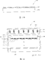
Fig. 4 is the diagrammatic elevation view of first exemplary embodiment of the mold pressing of example manufacturing system and solidified cell 500 and 600, and Fig. 5 is the process flow chart of the operation of being carried out in the mold pressing of Fig. 4 and solidified cell first embodiment.
With reference to figure 4, mold pressing unit 500 comprises mold pressing chamber 510, the first substrate supporting unit 520 and pushes unit 540, and solidified cell 600 comprises curing room 610, the second substrate supporting unit 620 and curing source unit 630.
The mold pressing chamber 510 of mold pressing unit 500 provides the wherein space of the various parts of installation unit.The first substrate supporting unit 520 is arranged in the mold pressing chamber 510, and is used to support the substrate 2000 that is carried in the mold pressing chamber 510.In this specific embodiment, substrate 2000 is meant on it that cell processing that the unit by in front for example carries out in cleaning unit, sedimentation unit and the coating unit has formed the substrate of thin metal film layer and photoresist in advance in regular turn.
On a surface of die 530, form strip pattern (not shown) with selected live width and distance between centers of tracks.Die 530 is used for strip pattern is transferred to the photoresist layer that is applied on the substrate.Illustrate in greater detail the structure and the manufacture method thereof of die 530 below with reference to Figure 12 to 15.
In the specific embodiment of Fig. 4, because the first substrate supporting unit 520 is arranged in the bottom part of mold pressing chamber 510, and push in 540 disposed thereon the parts in unit, the unit of pushing 540 is pressed on the substrate 2000 by making die 530 move down a die 530 towards the first substrate supporting unit 520.Yet the moving direction of die 530 is not limited.For example, for selecting among the embodiment, can make the first substrate supporting unit 520 and the place-exchange of pushing unit 540, promptly, push unit 540 and can be arranged in the bottom part of mold pressing chamber 510, and the first substrate supporting unit 520 can disposed thereon in the part.Because the result of this arrangement can prevent that impurity from dropping on the substrate, thereby can make substrate because the minimize contamination of impurity.
Illustrate in greater detail the technology of making wire-grid polarizer with first exemplary embodiment of the mold pressing of Fig. 4 and solidified cell 500 and 600 below with reference to Figure 4 and 5.
At first, the substrate 2000 that forms thin metal film layer and photoresist on it in regular turn is carried to mold pressing unit 500, and is placed on securely on the first substrate supporting unit 520, make die 530 be arranged on substrate 2000 tops and aim at it (Fig. 5, S510).
When die 530 is aligned in substrate 2000 tops, by pushing on the photoresist on the upper face that unit 540 is pressed downwardly onto die 530 substrate 2000 (S520).
The substrate 2000 that die 530 has been pressed on it is carried to solidified cell 600 (S530) by middle carrier unit 1000 then, and be placed on securely on the second substrate supporting unit 620 making under the pressure die 530 supine situations thereon, curing source unit 630 is by for example solidifying photoresist (S540) on the substrate 2000 with UV light or hot irradiation substrate then.When finishing photoresist curing processing, die 530 separates (S550) and turns back to mold pressing unit 500 from substrate and is used to reuse.
After substrate 2000 is removed die 530, substrate is carried to etching unit 700 (see figure 1)s in the direct downstream of solidified cell 600 to carry out subsequent treatment thereon.
Fig. 6 A and 6B are respectively the diagrammatic elevation view and the block diagrams of second exemplary embodiment of the mold pressing of example manufacturing system and solidified cell 500 and 600, and Fig. 7 is the process flow chart of the operation of being carried out in second embodiment of the mold pressing of Fig. 6 A and 6B and solidified cell.
Second embodiment of Fig. 6 A to 7 is different with first exemplary embodiment of Figure 4 and 5 to be to use a plurality of dies, and in addition, other is identical.Therefore, following argumentation mainly concentrates in two differences between the embodiment.
With reference to figure 6A and 6B, the mold pressing unit 500 of second embodiment comprises mold pressing chamber 510, the first substrate supporting unit 520, die 530, pushes unit 540 and die apotheca 550, and solidified cell 600 comprises curing room 610, the second substrate supporting unit 620 and curing source unit 630.
The mold pressing chamber 510 of mold pressing unit 500 provides the space of the various parts that mold pressing unit 500 wherein is set, and the first substrate supporting unit 520 is arranged in the mold pressing chamber 510, and is used to support the substrate 2000 that is carried in the mold pressing chamber 510.On a surface of die 530, form strip pattern (not shown) with selected live width and distance between centers of tracks.Die 530 is used for strip pattern (striped pattern) is transferred to the photoresist layer that is applied on the substrate, in the specific embodiment of institute's example, uses a plurality of dies by the mode that illustrates below.
In the part of the top of mold pressing chamber 510, be provided with and push unit 540, and be used for die 530 being pressed onto substrate 2000 by moving up and down die 530.Die apotheca 550 store other, die independently, that is, be not arranged on the die in the mold pressing chamber 510 of mold pressing unit 500, and be used for when needing, providing the die of these waits to mold pressing chamber 510.
Should understand, because the substrate that is molded in mold pressing unit 500 is carried to solidified cell 600 in the die 530 that is pressed onto on it, so in mold pressing chamber 510, do not stay die.As a result, be next substrate of mold pressing, the die that must wait for after finishing photoresist curing in solidified cell 600 handles, separates in solidified cell from substrate is got back to mold pressing chamber 510 by delivery.Yet, in the specific embodiment of Fig. 6 A, when die apotheca 550 is added to mold pressing unit 500 and one or more extra die is provided therein, needn't wait until that employed die is returned by delivery on the substrate in the solidified cell after finishing the curing processing, because when being cured processing, can be waiting for that another die in the die apotheca is carried to die chamber 510, therefore can reduce the stand-by period from apotheca.
Illustrate in greater detail the technology that second embodiment that utilizes mold pressing and solidified cell 500 and 600 makes wire-grid polarizer below with reference to Fig. 6 A to 7.
At first, the substrate 2000 that forms thin metal film layer and photoresist layer on it in regular turn is carried to mold pressing unit 500, and is placed on securely on the first substrate supporting unit 520.Die 530 is arranged on substrate 2000 tops and aim at it (Fig. 7, S710).When die 530 is aligned in substrate 2000 tops, die 530 is pressed onto (S720) on the substrate 2000 by pushing unit 540.
The substrate 2000 that die 530 has been pressed onto on it is carried to solidified cell 600 (S730) by middle carrier unit 1000 then.Simultaneously, another die delivery progressive die that is stored in the die apotheca 550 is pressed chamber 510, and begin to prepare next substrate of mold pressing queuing.
The substrate 2000 that has been pressed onto die 530 on it and has been carried to solidified cell 600 is placed on the second substrate supporting unit 620 securely, and with curing source unit 630 by its irradiation UV light or heat being solidified the photoresist (S740) on the substrate.When finishing the processing of solidifying photoresist, die 530 separates (S750) from substrate.The die 530 that separates is then got back to die apotheca 550 by delivery and is stored in wherein, and etching unit 700 (see figure 1)s that substrate 2000 is carried in solidified cell 600 direct downstreams are used for subsequent treatment.
Fig. 8 is the diagrammatic elevation view of the 3rd exemplary embodiment of the mold pressing of example manufacturing system and solidified cell 500 and 600, and Fig. 9 is the process flow chart of the operation of being carried out in the 3rd embodiment of the mold pressing of Fig. 8 and solidified cell.
Fig. 8 is similar to its first and second embodiment that introduces above with 600 the 3rd embodiment with solidified cell 500 with 9 mold pressing, but difference is that each is cured processing at mold pressing unit and solidified cell, and the asynchronism(-nization) that in the 3rd embodiment die is separated with substrate.Therefore, following argumentation mainly concentrates on the 3rd embodiment in structure and operational difference.
The photoresist that is applied on the substrate in coating unit 400 (see figure 1)s that are arranged in 500 upstreams, mold pressing unit can comprise " mixing " photoresist,, wherein mixes the photoresist of curable photoresist of UV and thermosetting photoresist that is.In this case, the curable photoresist of UV can comprise for example acrylic polymer, and the thermosetting photoresist can comprise for example epoxy polymer.
Consider above-mentioned situation, the mold pressing unit 500 of Fig. 8 and 9 the 3rd embodiment is provided with the UV light source 560 that is used to solidify the curable part of UV of mixing the photoresist potpourri extraly.UV light source 560 can be provided in pushing in the unit 540 in the top part that is arranged at mold pressing chamber 510.Yet the position that UV light source 560 is set is not limited thereto, and UV light source 560 can be arranged on various other positions in the mold pressing chamber 510.
The curing source of the solidified cell 600 of the 3rd embodiment comprises the well heater 635 that is used to solidify the thermosetting part of mixing the photoresist potpourri.
Illustrate in greater detail the technology that the 3rd exemplary embodiment of utilizing mold pressing and solidified cell 500 and 600 is made wire-grid polarizer below with reference to Fig. 8 and 9.
At first, the substrate 2000 that forms thin metal film layer and photoresist on it in regular turn is carried to mold pressing unit 500, and is placed on securely on the first substrate supporting unit 520.Then die 530 is arranged on substrate 2000 tops and aims at (S910) with it.In this specific embodiment, as mentioned above, formed photoresist is the mixing photoresist that the potpourri by curable photoresist of UV and thermosetting photoresist constitutes on substrate.
When die 530 was aligned in substrate 2000 tops, utilization was pushed unit 540 die 530 is pressed onto (S920) on the substrate 2000.In this specific embodiment, die 530 is consistent with substrate 2000 dimensionally, and therefore, the pattern of die is transferred on the substrate in a press operation.
Then, partly solidified photoresist, that is, the UV light source 560 of pushing unit 500 by utilization is solidificated in the UV photoirradiation to the substrate the curable part of UV (S930) of the mixing photoresist potpourri on the substrate.From substrate, separate die 530 (S940) then.
Then by middle carrier unit 1000 being carried to solidified cell 600 (S950) from the substrate 2000 of wherein removing die 530, and be placed on securely on the second substrate supporting unit 620, photoresist on the full solidification substrate then, that is, hot irradiation is solidificated in thereon the thermosetting part (S960) of the mixing photoresist potpourri on the substrate by the well heater 635 that utilizes solidified cell 600.Then substrate 2000 is carried to etching unit 700 (see figure 1)s that are arranged on solidified cell 600 downstreams and is used for subsequent treatment.
As mentioned above, when the mixing photoresist that is made of curable photoresist of UV and thermosetting photoresist is used as photoresist, if being forced into to mix, die also uses UV photoirradiation photoresist on the photoresist then, the curable part of the UV of photoresist is cured, so its shape becomes fixing.Under this condition, although die with mix photoresist and separate, the cured portion of photoresist is keeping transferring to pattern on it by die effectively.When photoresist being carried to solidified cell and handle to solidify mixing the thermosetting part of photoresist potpourri, mix photoresist thus by full solidification by heat curing.
Therefore, when in the 3rd embodiment of mold pressing and solidified cell 500 and 600, using above-mentioned " two curing " method respectively, can be the processed in units time decreased to minimum.
Figure 10 is the diagrammatic elevation view of the 4th exemplary embodiment of the mold pressing of example manufacturing system and solidified cell, and Figure 11 is the process flow chart of the operation of being carried out in the 4th embodiment of the mold pressing of Figure 10 and solidified cell.
Except that the size of the die that is provided than the size of substrate little, Figure 10 is identical with the 3rd embodiment of above-mentioned Fig. 8 and 9 with 11 the 4th exemplary embodiment.Therefore, following argumentation mainly concentrates in the difference of the structure of the 4th embodiment and operation.
With reference to Figure 10, the mold pressing unit 500 of the 4th embodiment comprises mold pressing chamber 510, the first substrate supporting unit 520, die 530, pushes unit 540, UV light source 560 and UV light blocking unit 570, and solidified cell 600 comprises curing room 610, the second substrate supporting unit 620 and well heater 635.
The mixing photoresist that is made of the potpourri of curable photoresist of UV and thermosetting photoresist is as the photoresist that is applied in coating unit 400 (see figure 1)s that are arranged in 500 upstreams, mold pressing unit on the substrate.Mold pressing unit 500 is provided with UV light source 560 to be solidificated in the curable part of UV of mixing photoresist potpourri set on the substrate.
As mentioned above, employed die 530 is littler than substrate 2000 in the 4th exemplary embodiment.Therefore, must repeat die 530 is pressed in technology at least twice on the substrate, with up hill and dale on the photoresist of the design transfer of littler die 530 to the bigger substrate.Should understand, if use die 530 is pressed on the mixing photoresist of substrate and also use the above-mentioned pair curing technology of UV light source 560 then with its curing, the zone that must make not the photoresist of being pressed by die 530 so was cured before with the die impression so that prevent them not by the UV photoirradiation.Therefore, UV light blocking unit 570 is set in the part of the bottom of UV light source 560, with a part of UV light on stopping from UV light source 560 irradiation to photoresist.In the present embodiment, UV light blocking unit 570 by metal material for example the metal film made of chromium or aluminium form.
Illustrate in greater detail the technology that the 4th exemplary embodiment of utilizing mold pressing and solidified cell 500 and 600 is made wire-grid polarizer below with reference to Figure 10 and 11.
At first, the substrate 2000 that forms thin metal film layer and photoresist on it in regular turn is carried to mold pressing unit 500, and is placed on securely on the first substrate supporting unit 520.Then die 530 is arranged on substrate 2000 tops and aim at it (Figure 11, S1110).As mentioned above, in this embodiment, formed photoresist comprises the mixing photoresist on substrate, i.e. the potpourri of curable photoresist of UV and thermosetting photoresist.And die 530 is dimensionally less than substrate 2000.
When die 530 was aligned in substrate 2000 tops at first, utilization was pushed unit 540 die 530 is pressed downwardly onto (S1120) on the substrate 2000.Then, by utilizing UV light source 560, UV light only irradiation be the curable part of UV of having pressed partly solidified mixing photoresist potpourri on the zone of die on it to a part of substrate, the partly solidified region blocks UV light (S1130) that do not have that uses UV light blocking unit 570 to come from photoresist.Separate die 530 (S1140) then the partly solidified district of the photoresist from substrate.
Then, carry out above-mentioned processing step repeatedly and repeatedly, transferred to up to required mold pattern on the whole zone of the photoresist on the substrate (S1150).Then, last repeatedly after, promptly, after required pattern has been formed in the whole surface of the photoresist on the substrate 2000, the above-mentioned selectivity UV irradiation of its selection area is passed through by partly solidified in the whole surface of photoresist, by middle carrier unit 1000 substrate 2000 that die 530 has separated from it is carried to solidified cell 600 (S1160).
Figure 12 is the schematic cross section according to the exemplary embodiment of die of the present invention.Figure 13 is the diagrammatic elevation view that is attached to a plurality of units die on the parent plate.Figure 14 is a schematic cross section of selecting exemplary embodiment according to the confession of die of the present invention.
Comprise parent plate 531, a plurality of magnet 532 and a plurality of units die 535 with reference to Figure 12 and 13, the first exemplary dies 530.
As shown in figure 12, first and second magnets with opposite polarity are that arctic magnet 532a and South Pole magnet 532b are embedded in the surface of parent plate 531 in mode adjacent, that replace.Then a plurality of units die 535 is attached on the surface of the parent plate 531 that has wherein embedded magnet 532.In this embodiment, on constituent parts die 535, form meticulous, strip pattern (not shown).
With reference to Figure 13 in more detail the unit's of description die 535 be attached to principle on the parent plate 531.In Figure 13, arctic magnet 532a and South Pole magnet 532b arrange in the mode that replaces in the same plane of parent plate 531 lower surface.In this structure, magnetic flux flows to its South Pole from the arctic of magnet.According to the Lorentz law of magnetic theory, in such arrangement, along the direction perpendicular to flow direction, the direction that promptly extends to the top of structure along the bottom from structure produces electrostatic attraction, shows as the arrow among Figure 13.When producing electrostatic attraction according to this theory, metal material is when will be attached to this lower surface statically when the lower surface of parent plate 531 is placed.
Silicon or quartz wafer all can be used as the substrate of unit die 535.Because silicon wafer itself is conductor, as shown in Figure 12, the unit die 535 that is formed by silicon wafer will be attached on the parent plate and not need coated with conductive metal level thereon.Yet, when quartz wafer is used the substrate of office's die 535, because quartz wafer is an electrically insulating material, thus on the attaching surface of unit die 535, additionally form conductive metal layer 538, as shown in figure 14.In addition, even when silicon wafer is used as substrate, also can form conductive metal layer 538 alternatively thereon to strengthen electrostatic attraction.
Therefore, when the electrostatic attraction by utilizing embedded magnet is attached to a plurality of units die 535 when making big die on the parent plate 531, this technology can be advantageously utilised in abrasive indoor or even vacuum chamber in.Like this, although known air-breathing (air induction) or " vacuum cup (vacuumchuck) " method can not be used in a vacuum, but the electrostatic attraction method can even be applied in the vacuum environment, even and resulting die assembling when long-term the use, also be not easy disturbed because the intensity of electrostatic attraction keeps substantial constant.
Figure 15 A to 15D is the schematic section of substrate, respectively example be used to make operation in turn according to the exemplary embodiment of the method for unit of the present invention die.With reference to figure 15A to 15D, at first, on the surface of the unit die substrate 536 that forms by circular silicon or quartz wafer, form along the fine pattern of the metal wire of a direction extension, promptly wire grid pattern 537, shown in Figure 15 A.
Shown in Figure 15 B, the whole surface that forms the unit die substrate 536 of wire grid pattern 537 thereon forms protective seam 539.In this specific embodiment, form protective seam 539 by applying one deck organic material that constitutes by photoresist or soluble polymer, cure organic material layer then.
Then, shown in Figure 15 C, utilize diamond cut off wheel for example or laser instrument that the unit die substrate 536 that forms wire grid pattern 537 and protective seam 539 on it is cut into rectangle or square.
After the as above unit's of cutting die substrate 536, by the manufacturing of 539 unit's of the finishing dies 535 of the protective seam on the unit's of removing die, shown in Figure 15 D.
When carrying out above-mentioned operation, that is, when forming protective seam, cutting unit die substrate and removing protective seam then, prevented that the wire grid pattern on the substrate from being polluted or damage during cutting action by above-mentioned order.
Figure 16 is the diagrammatic elevation view of exemplary embodiment of mold pressing unit that is used to make the example system of wire-grid polarizer of the present invention.
The gaseous tension applying unit comprise gas supply source (not shown) and in the wall of pushing chamber 541 formed gas injection hole 543, described gas supply source is arranged on that to push chamber 541 outside and be configured to supply and be used for being injected into the gas of pushing chamber 541.
Gaseous tension amending unit 545 comprises and is arranged on a plurality of spring members (spring member) of pushing 541 inside, chamber symmetrically.
When gas by the wall of pushing chamber 541 in formed gas injection hole 543 be injected into when pushing the chamber, the pressure of gas may impose on die inconsistently, because pressure imposes on die partly according to the position of gas injection hole, it may cause die to be forced on the substrate 520 in inconsistent mode.
Yet, even gaseous tension is applied on the surface of die 530 inconsistently, promptly, may be big in the specific region of die than in other zone, thereby cause die in those positions, to be pressed more and cause inconsistent displacement, but gaseous tension amending unit 545 also comprises a plurality of spring members, the balance that it comes the compensatory pressure difference and be used for recovering institute's applied pressure by the difference in the skew of offsetting the die that is caused by unbalanced pressure.
And, the gaseous tension applying unit almost moment injecting gas enter and push chamber 541, or alternatively can be with discontinuous, the step that increases in the gas flood chamber.Therefore, it can be exerted pressure to pressing the chamber with one or more steps.
Can in the sidewall of the mold pressing chamber 510 of mold pressing unit 500, be provided for opening and closing the opening 515 of mold pressing chamber.
According to the exemplary embodiment of the invention described above,, can greatly reduce the processing time that is used to make wire-grid polarizer by arrange the each processing unit of arranging to be used to make the system of polarizer by tandem.In addition, by utilizing electrostatic force a plurality of units die is attached on the parent plate, system and method for the present invention can increase the size of wire-grid polarizer and the precision that can improve manufacturing process, thereby the size of die is increased.
So far, it will be understood by those skilled in the art that without departing from the spirit and scope of the present invention, can make and it is carried out many modifications, replacement and change at the system and method that is used for making wire-grid polarizer of the present invention.Therefore, scope of the present invention should not be limited to example shown here and specific embodiment explanation, because they in fact only are exemplary, but should fully match with after this additional claim and functional equivalent thereof.
The application requires to inject for reference in full herein in the right of priority of the korean patent application No.10-2006-0076959 of application on August 16th, 2006.
Claims (37)
1. system that is used to make wire-grid polarizer comprises:
Be used on substrate, forming the sedimentation unit of thin metal film layer;
The coating unit that is used on described thin metal film layer, applying photoresist and is used to cure described photoresist;
The mold pressing unit comprises the die that has formed pattern on it, be used for being pressed onto on the described photoresist of described substrate to described die and thus the design transfer of described die to described photoresist; And
Be used to solidify the solidified cell of described photoresist.
2. system as claimed in claim 1 also comprises:
The etching unit that is used for the described thin metal film layer of etching; And
Be used to remove the incineration unit of described photoresist.
3. system as claimed in claim 2 also comprises:
Be used for described substrate is loaded into described intrasystem load units;
Be used to clean the cleaning unit of described substrate;
Be used for from the unloading unit of the described substrate of described system's unloading; And
The a plurality of carrier units that are used for the described substrate of delivery in described system.
4. system as claimed in claim 3, wherein in the following order each other tandem ground arrange described unit: described load units, described cleaning unit, described sedimentation unit, described coating unit, described mold pressing unit, described solidified cell, described etching unit, described incineration unit and described unloading unit, and wherein each described carrier unit is set between the phase adjacency pair of other unit.
5. system as claimed in claim 1, wherein said mold pressing unit also comprises:
The mold pressing chamber;
Be arranged in the described mold pressing chamber and be configured the first substrate supporting unit that supports described substrate; And
To described die described die is pressed onto the unit of pushing on the described photoresist on the described substrate thereby be used to exert pressure.
6. system as claimed in claim 5, wherein said die comprises:
Parent plate;
Arrange and be embedded in the opposite polarity that has in the first surface of described parent plate in the mode that replaces.First and second magnets; And
Be attached to a plurality of units die of the described first surface of described parent plate statically.
7. system as claimed in claim 6, wherein each unit die comprises:
Unit die substrate with first and second opposite surfaces; And
Fine pattern in the direction extension in the described first surface upper edge of described unit die substrate.
8. system as claimed in claim 7, wherein said unit die also is included in the metal conducting layer on the described second surface of described unit die substrate.
9. system as claimed in claim 7, wherein this unit die substrate comprises silicon wafer or quartz wafer.
10. system as claimed in claim 5, the wherein said unit of pushing comprises:
Push the chamber; And
Be used for that gas is injected into described pressure chamber and the inside of described pressure chamber applied the gaseous tension applying unit of gaseous tension.
11., wherein saidly push the conforming gaseous tension amending unit that the unit also comprises the described gaseous tension that is used to keep to be applied to described inside of pushing the chamber as the system of claim 10.
12. as the system of claim 11, wherein said gas applying unit comprises:
The gas supply source is arranged on and describedly pushes outdoor and configuration is supplied and is used to be injected into the described gas of pushing the chamber; And
At the described gas injection hole that forms in the wall of chamber of pushing.
13. as the system of claim 11, wherein said gaseous tension amending unit comprises and is arranged on described a plurality of spring members of pushing chamber interior.
14. system as claimed in claim 5 also comprises the die apotheca, is used to store the die of wait.
15. as the system of claim 1 or 5, wherein said solidified cell comprises:
Curing room;
Be arranged on and also construct the second substrate supporting unit that supports described substrate in the described curing room; And
Be used to solidify the curing source unit of described photoresist.
16. as the system of claim 15, wherein said photoresist is made of curable photoresist of UV or thermosetting photoresist.
17. as the system of claim 16, wherein said curing source unit comprises UV light source or well heater.
18. as the system of claim 15, wherein said photoresist constitutes by mixing photoresist, this mixing photoresist is made of the potpourri of curable photoresist of UV and thermosetting photoresist.
19. as the system of claim 18, wherein:
Described mold pressing unit also comprises the UV light source of the curable photoresist of described UV that is used to solidify described mixing photoresist; And
The described curing source unit of described solidified cell comprises the well heater of the described thermosetting photoresist that is used to solidify described mixing photoresist.
20. as the system of claim 19, wherein said mold pressing unit also comprises the UV light blocking unit that is used to stop from the described UV light of part of described UV light source institute irradiation.
21. as the system of claim 20, wherein said UV light blocking unit comprises metal film.
22. system as claimed in claim 2, the described thin metal film layer of wherein said etching unit dry etching.
23. a method that is used to make wire-grid polarizer, this method comprises:
Substrate is provided;
On described substrate, form the thin metal film layer;
Apply photoresist to described thin metal film layer;
Cure the described substrate that has been applied in described photoresist;
The die that has pattern on it is provided;
Die is aimed at the described photoresist of described substrate;
Thereby described die is pressed onto on the described photoresist of described substrate the described design transfer of described die to described photoresist;
Solidify described photoresist;
Described die is separated with described substrate; And
The described thin metal film layer of the described substrate of etching.
24., wherein use photoresist and comprise to described thin metal film layer and apply the curable photoresist of UV or thermosetting photoresist to described thin metal film layer as the method for claim 23.
25., wherein solidify described photoresist and comprise irradiation UV light or execute and be heated to described photoresist as the method for claim 24.
26. as the method for claim 23, wherein providing die to comprise provides a plurality of dies.
27. a method that is used to make wire-grid polarizer, this method comprises:
Substrate is provided;
On described substrate, form the thin metal film layer;
Apply photoresist to described thin metal film layer;
Cure the described substrate that has been applied in described photoresist;
The die that has pattern on it is provided;
Described die is aimed at the described photoresist of described substrate,
Thereby described die is pressed on the described photoresist of described substrate the described design transfer of described die to described photoresist;
Partly solidified described photoresist;
Described die is separated with described substrate;
The described photoresist of full solidification; And
The described thin metal film layer of the described substrate of etching.
28., wherein apply photoresist and comprise to described thin metal film layer and apply mixing photoresist that the potpourri by curable photoresist of UV and thermosetting photoresist constitutes to described thin metal film layer as the method for claim 27.
29. as the method for claim 28, wherein partly solidified described photoresist comprises with the described photoresist of UV photoirradiation.
30. as the method for claim 29, wherein
Providing die to comprise provides the die littler than described substrate; And
Partly solidified described photoresist comprises with the zone of having been pressed described die on its of the described substrate of UV photoirradiation.
31. method as claim 30, wherein saidly make on described die and described base plate alignment, the described described photoresist that described die is pressed in described substrate, described partly solidified described photoresist and describedly described die is separated with described substrate repeated repeatedly, be transferred to the whole zone of the described photoresist of described substrate up to the described pattern of described die.
32. as the method for claim 28, wherein the described photoresist of full solidification comprises executing and is heated to described photoresist.
33. as the method for claim 23 or 27, wherein providing die to comprise provides a plurality of units die.
34., wherein provide a plurality of units die to comprise as the method for claim 33:
Parent plate is provided;
Embed first and second magnets in the first surface of parent plate, described magnet has opposite polarity and arranges in the mode that replaces; And
The described first surface of a plurality of units die electrostatic adhesion to described parent plate.
35., wherein provide a plurality of units die to comprise as the method for claim 33:
Unit with first and second opposite surfaces die substrate is provided;
On the described first surface of described unit die substrate, form fine pattern;
Above the described first surface of described unit die substrate and the described fine pattern on it, form protective seam;
Cut described unit die substrate; And
Remove described protective seam.
36., wherein form protective seam and comprise as the method for claim 35:
Apply one deck organic material layer of constituting by photoresist or soluble polymer described first surface and described fine pattern on it to described unit die substrate; And
Cure described organic material layer.
37., form metal conducting layer on the described second surface that wherein provides a plurality of units die also to be included in described unit die substrate as the method for claim 35.
Applications Claiming Priority (2)
| Application Number | Priority Date | Filing Date | Title |
|---|---|---|---|
| KR76959/06 | 2006-08-16 | ||
| KR1020060076959A KR20080015536A (en) | 2006-08-16 | 2006-08-16 | System and method for manufacturing wire grid polarizer |
Publications (1)
| Publication Number | Publication Date |
|---|---|
| CN101126894A true CN101126894A (en) | 2008-02-20 |
Family
ID=38962156
Family Applications (1)
| Application Number | Title | Priority Date | Filing Date |
|---|---|---|---|
| CNA2007100081174A Pending CN101126894A (en) | 2006-08-16 | 2007-01-26 | Systems and methods for manufacturing wire grid polarizers |
Country Status (6)
| Country | Link |
|---|---|
| US (1) | US20080041816A1 (en) |
| EP (1) | EP1914571A3 (en) |
| JP (1) | JP2008046580A (en) |
| KR (1) | KR20080015536A (en) |
| CN (1) | CN101126894A (en) |
| TW (1) | TW200811487A (en) |
Cited By (4)
| Publication number | Priority date | Publication date | Assignee | Title |
|---|---|---|---|---|
| CN102044476B (en) * | 2009-10-13 | 2013-06-19 | 中芯国际集成电路制造(上海)有限公司 | Forming method of metal pattern |
| CN109270620A (en) * | 2018-11-16 | 2019-01-25 | 京东方科技集团股份有限公司 | The production method and display panel of wire grating polarizing film |
| CN111149025A (en) * | 2017-09-27 | 2020-05-12 | 日本电气硝子株式会社 | Glass plate with optical film and method for producing same |
| WO2020124890A1 (en) * | 2018-12-20 | 2020-06-25 | 深圳市华星光电半导体显示技术有限公司 | Manufacturing method for wire grid type polarizer, and transparent display apparatus |
Families Citing this family (17)
| Publication number | Priority date | Publication date | Assignee | Title |
|---|---|---|---|---|
| TWI481496B (en) * | 2007-12-19 | 2015-04-21 | Heptagon Micro Optics Pte Ltd | Manufacturing optical elements |
| JP5077764B2 (en) | 2008-04-22 | 2012-11-21 | 富士電機株式会社 | Imprint method and apparatus |
| JP5370806B2 (en) * | 2008-04-22 | 2013-12-18 | 富士電機株式会社 | Imprint method and apparatus |
| JP5279397B2 (en) * | 2008-08-06 | 2013-09-04 | キヤノン株式会社 | Imprint apparatus, imprint method, and device manufacturing method |
| JP5149244B2 (en) * | 2009-06-19 | 2013-02-20 | 東京エレクトロン株式会社 | IMPRINT SYSTEM, IMPRINT METHOD, PROGRAM, AND COMPUTER STORAGE MEDIUM |
| KR20120075877A (en) * | 2010-12-29 | 2012-07-09 | 삼성전자주식회사 | Liquid crystal display panel and apparautus thereof |
| JP2013020182A (en) * | 2011-07-13 | 2013-01-31 | Asahi Kasei E-Materials Corp | Wire grid polarizing plate and method for manufacturing wire grid polarizing plate |
| US20130043956A1 (en) * | 2011-08-15 | 2013-02-21 | Honeywell International Inc. | Systems and methods for a nanofabricated optical circular polarizer |
| KR20140030382A (en) | 2012-08-27 | 2014-03-12 | 삼성디스플레이 주식회사 | Liquid crystal display and fabrication method of the same |
| CN104058362B (en) * | 2013-03-21 | 2017-06-27 | 无锡华润上华半导体有限公司 | The processing method of microelectromechanical systems |
| KR102056902B1 (en) | 2013-05-29 | 2019-12-18 | 삼성전자주식회사 | Wire grid polarizer and liquid crystal display panel and liquid crystal display device having the same |
| KR102089661B1 (en) | 2013-08-27 | 2020-03-17 | 삼성전자주식회사 | Wire grid polarizer and liquid crystal display panel and liquid crystal display device having the same |
| KR101729683B1 (en) * | 2015-09-16 | 2017-04-25 | 한국기계연구원 | Manufacturing method of wire grid polarizer |
| JP6725097B2 (en) | 2016-01-27 | 2020-07-15 | エルジー・ケム・リミテッド | Film mask, manufacturing method thereof, pattern forming method using the same, and pattern formed using the same |
| EP3410214A4 (en) | 2016-01-27 | 2019-01-23 | LG Chem, Ltd. | Film mask, method for manufacturing same, and method for forming pattern using film mask and pattern formed thereby |
| CN108351603A (en) | 2016-01-27 | 2018-07-31 | 株式会社Lg化学 | Film mask, preparation method and the pattern forming method using film mask |
| KR102022268B1 (en) * | 2018-02-14 | 2019-09-19 | 한국기계연구원 | Imprint apparatus using instantaneous heating and liquid transfer, the method |
Family Cites Families (10)
| Publication number | Priority date | Publication date | Assignee | Title |
|---|---|---|---|---|
| JP3152257B2 (en) * | 1992-08-10 | 2001-04-03 | 株式会社タツノ・メカトロニクス | Refueling device |
| US7218465B1 (en) * | 2002-06-28 | 2007-05-15 | Seagate Technology Llc | Magnetic media patterning via contact printing utilizing stamper having magnetic pattern formed in non-magnetic substrate |
| KR100484088B1 (en) * | 2002-12-06 | 2005-04-20 | 삼성전자주식회사 | Die attach and cure in line apparatus for multi chip package |
| WO2004092085A2 (en) * | 2003-04-14 | 2004-10-28 | National Graphics, Inc. | Lenticular images formed on selected images portions |
| JP4295592B2 (en) * | 2003-09-30 | 2009-07-15 | 大日本印刷株式会社 | Production method of duplicate plate |
| JP2005153091A (en) * | 2003-11-27 | 2005-06-16 | Hitachi Ltd | Transfer method and transfer device |
| KR100624414B1 (en) * | 2003-12-06 | 2006-09-18 | 삼성전자주식회사 | Manufacturing Method of Diffractive Lens Array and UV Dispenser |
| KR20050075580A (en) * | 2004-01-16 | 2005-07-21 | 엘지전자 주식회사 | Fabricating method of larger area stamp with nano imprint lithography |
| US20060056024A1 (en) * | 2004-09-15 | 2006-03-16 | Ahn Seh W | Wire grid polarizer and manufacturing method thereof |
| JP2006084776A (en) * | 2004-09-16 | 2006-03-30 | Lg Electronics Inc | Wire-grid polarizer and its manufacturing method |
-
2006
- 2006-08-16 KR KR1020060076959A patent/KR20080015536A/en not_active Application Discontinuation
- 2006-11-27 JP JP2006317914A patent/JP2008046580A/en active Pending
- 2006-12-29 US US11/648,092 patent/US20080041816A1/en not_active Abandoned
-
2007
- 2007-01-26 CN CNA2007100081174A patent/CN101126894A/en active Pending
- 2007-04-25 TW TW096114603A patent/TW200811487A/en unknown
- 2007-08-16 EP EP07016076A patent/EP1914571A3/en not_active Withdrawn
Cited By (5)
| Publication number | Priority date | Publication date | Assignee | Title |
|---|---|---|---|---|
| CN102044476B (en) * | 2009-10-13 | 2013-06-19 | 中芯国际集成电路制造(上海)有限公司 | Forming method of metal pattern |
| CN111149025A (en) * | 2017-09-27 | 2020-05-12 | 日本电气硝子株式会社 | Glass plate with optical film and method for producing same |
| CN109270620A (en) * | 2018-11-16 | 2019-01-25 | 京东方科技集团股份有限公司 | The production method and display panel of wire grating polarizing film |
| US11307341B2 (en) | 2018-11-16 | 2022-04-19 | Boe Technology Group Co., Ltd. | Method for manufacturing metal wire grid polarizer and display panel |
| WO2020124890A1 (en) * | 2018-12-20 | 2020-06-25 | 深圳市华星光电半导体显示技术有限公司 | Manufacturing method for wire grid type polarizer, and transparent display apparatus |
Also Published As
| Publication number | Publication date |
|---|---|
| EP1914571A2 (en) | 2008-04-23 |
| EP1914571A3 (en) | 2010-01-20 |
| US20080041816A1 (en) | 2008-02-21 |
| TW200811487A (en) | 2008-03-01 |
| KR20080015536A (en) | 2008-02-20 |
| JP2008046580A (en) | 2008-02-28 |
Similar Documents
| Publication | Publication Date | Title |
|---|---|---|
| CN101126894A (en) | Systems and methods for manufacturing wire grid polarizers | |
| KR100806513B1 (en) | Method of patterning conductive layers, method of manufacturing polarizers, and polarizers manufactured using the same | |
| JP4824487B2 (en) | LED package manufacturing method | |
| US8909009B2 (en) | Light guides having enhanced light extraction | |
| US20080064131A1 (en) | Light emitting apparatus and method for the same | |
| US20090061552A1 (en) | Light emitting apparatus and method for the same | |
| US9952367B2 (en) | Wire grid polarizer and manufacturing method thereof, and display device | |
| JP2003094445A (en) | Manufacturing method for fine structure, manufacturing method for device equipped with the fine structure, fine structure by the manufacturing method, device for manufacturing the fine structure, and device for manufacturing device equipped with the fine structure | |
| US7796336B2 (en) | Lens, lens array and method for making lens array | |
| TW200632577A (en) | Exposure device and manufacturing method of device | |
| US20120257292A1 (en) | Wafer Level Lens Module and Method for Manufacturing the Wafer Level Lens Module | |
| KR101521730B1 (en) | Backlight module, display device and fabricating method of grid points on light guiding plate and light guiding plate | |
| WO2016107040A1 (en) | Wire-grid polarizer, manufacturing method therefor, and display device | |
| KR20060080476A (en) | Method for forming pattern on shadow-mask | |
| CN101963760B (en) | Coating apparatus having coater chuck | |
| RU2432417C1 (en) | Device for sputtering thin layers in multi-layer items in vacuum | |
| US6994951B1 (en) | Method of fabricating a stamper by half-tone technology | |
| KR101316742B1 (en) | Main frame manufacturing method for supporting lcd of smart phone | |
| US10042256B2 (en) | Silane coupling agent and method of manufacturing wire grid pattern using the same | |
| CN102392994A (en) | Back frame of panel display device, backlight system and panel liquid crystal display device | |
| US20090268302A1 (en) | Light blocking plate, lens module having same and method for making same | |
| KR101914454B1 (en) | Mold for optical sheet and manufacturing method therefor and, optical sheet manufactured using the mold | |
| US10910514B1 (en) | Molded etch masks | |
| KR101260939B1 (en) | Attaching module, Apparatus for attaching substrate and method for manufacturing attaching pad | |
| KR102489591B1 (en) | Deposition Apparatus |
Legal Events
| Date | Code | Title | Description |
|---|---|---|---|
| C06 | Publication | ||
| PB01 | Publication | ||
| C10 | Entry into substantive examination | ||
| SE01 | Entry into force of request for substantive examination | ||
| C02 | Deemed withdrawal of patent application after publication (patent law 2001) | ||
| WD01 | Invention patent application deemed withdrawn after publication |
Application publication date: 20080220 |