KR20060126712A - Gallium nitride material devices including an electrode-defining layer and methods of forming the same - Google Patents
Gallium nitride material devices including an electrode-defining layer and methods of forming the same Download PDFInfo
- Publication number
- KR20060126712A KR20060126712A KR1020067014242A KR20067014242A KR20060126712A KR 20060126712 A KR20060126712 A KR 20060126712A KR 1020067014242 A KR1020067014242 A KR 1020067014242A KR 20067014242 A KR20067014242 A KR 20067014242A KR 20060126712 A KR20060126712 A KR 20060126712A
- Authority
- KR
- South Korea
- Prior art keywords
- electrode
- gallium nitride
- nitride material
- material region
- forming layer
- Prior art date
Links
- 239000000463 material Substances 0.000 title claims abstract description 168
- JMASRVWKEDWRBT-UHFFFAOYSA-N Gallium nitride Chemical compound [Ga]#N JMASRVWKEDWRBT-UHFFFAOYSA-N 0.000 title claims abstract description 166
- 229910002601 GaN Inorganic materials 0.000 title claims abstract description 165
- 238000000034 method Methods 0.000 title claims abstract description 65
- 239000004065 semiconductor Substances 0.000 claims description 61
- 239000000758 substrate Substances 0.000 claims description 56
- 230000007704 transition Effects 0.000 claims description 28
- PXHVJJICTQNCMI-UHFFFAOYSA-N Nickel Chemical compound [Ni] PXHVJJICTQNCMI-UHFFFAOYSA-N 0.000 claims description 25
- 229910052751 metal Inorganic materials 0.000 claims description 25
- 239000002184 metal Substances 0.000 claims description 25
- 230000015572 biosynthetic process Effects 0.000 claims description 24
- 238000002161 passivation Methods 0.000 claims description 21
- 229910052710 silicon Inorganic materials 0.000 claims description 21
- 239000010703 silicon Substances 0.000 claims description 20
- 229910052759 nickel Inorganic materials 0.000 claims description 13
- 229910052737 gold Inorganic materials 0.000 claims description 10
- 239000010931 gold Substances 0.000 claims description 10
- PCHJSUWPFVWCPO-UHFFFAOYSA-N gold Chemical compound [Au] PCHJSUWPFVWCPO-UHFFFAOYSA-N 0.000 claims description 9
- -1 silicon nitride compound Chemical class 0.000 claims description 9
- 229910052581 Si3N4 Inorganic materials 0.000 claims description 8
- 229910052733 gallium Inorganic materials 0.000 claims description 5
- 229910052814 silicon oxide Inorganic materials 0.000 claims description 5
- GYHNNYVSQQEPJS-UHFFFAOYSA-N Gallium Chemical compound [Ga] GYHNNYVSQQEPJS-UHFFFAOYSA-N 0.000 claims description 4
- 230000007423 decrease Effects 0.000 claims description 4
- 239000000203 mixture Substances 0.000 claims description 3
- 238000001020 plasma etching Methods 0.000 claims description 3
- 239000010410 layer Substances 0.000 description 169
- XUIMIQQOPSSXEZ-UHFFFAOYSA-N Silicon Chemical compound [Si] XUIMIQQOPSSXEZ-UHFFFAOYSA-N 0.000 description 17
- 238000013461 design Methods 0.000 description 15
- 238000005530 etching Methods 0.000 description 13
- 238000000151 deposition Methods 0.000 description 12
- 230000015556 catabolic process Effects 0.000 description 11
- 230000008569 process Effects 0.000 description 11
- 230000008021 deposition Effects 0.000 description 10
- 229910045601 alloy Inorganic materials 0.000 description 8
- 239000000956 alloy Substances 0.000 description 8
- 230000005684 electric field Effects 0.000 description 8
- 230000007547 defect Effects 0.000 description 7
- 229910052757 nitrogen Inorganic materials 0.000 description 7
- 229910052782 aluminium Inorganic materials 0.000 description 6
- 230000000694 effects Effects 0.000 description 6
- 239000007772 electrode material Substances 0.000 description 6
- 238000012545 processing Methods 0.000 description 6
- 238000000059 patterning Methods 0.000 description 5
- 239000011347 resin Substances 0.000 description 5
- 229920005989 resin Polymers 0.000 description 5
- XKRFYHLGVUSROY-UHFFFAOYSA-N Argon Chemical compound [Ar] XKRFYHLGVUSROY-UHFFFAOYSA-N 0.000 description 4
- 150000001875 compounds Chemical class 0.000 description 4
- 230000006872 improvement Effects 0.000 description 4
- 230000001965 increasing effect Effects 0.000 description 4
- 229910052738 indium Inorganic materials 0.000 description 4
- 239000011229 interlayer Substances 0.000 description 4
- 150000002500 ions Chemical class 0.000 description 4
- HQVNEWCFYHHQES-UHFFFAOYSA-N silicon nitride Chemical compound N12[Si]34N5[Si]62N3[Si]51N64 HQVNEWCFYHHQES-UHFFFAOYSA-N 0.000 description 4
- VYPSYNLAJGMNEJ-UHFFFAOYSA-N Silicium dioxide Chemical compound O=[Si]=O VYPSYNLAJGMNEJ-UHFFFAOYSA-N 0.000 description 3
- 230000009286 beneficial effect Effects 0.000 description 3
- 239000013078 crystal Substances 0.000 description 3
- 239000007789 gas Substances 0.000 description 3
- 238000005468 ion implantation Methods 0.000 description 3
- 238000001465 metallisation Methods 0.000 description 3
- 238000012986 modification Methods 0.000 description 3
- 230000004048 modification Effects 0.000 description 3
- 238000004151 rapid thermal annealing Methods 0.000 description 3
- 238000004088 simulation Methods 0.000 description 3
- 235000012431 wafers Nutrition 0.000 description 3
- 239000004642 Polyimide Substances 0.000 description 2
- 229910052786 argon Inorganic materials 0.000 description 2
- QVGXLLKOCUKJST-UHFFFAOYSA-N atomic oxygen Chemical compound [O] QVGXLLKOCUKJST-UHFFFAOYSA-N 0.000 description 2
- 238000006243 chemical reaction Methods 0.000 description 2
- PMHQVHHXPFUNSP-UHFFFAOYSA-M copper(1+);methylsulfanylmethane;bromide Chemical compound Br[Cu].CSC PMHQVHHXPFUNSP-UHFFFAOYSA-M 0.000 description 2
- 238000005538 encapsulation Methods 0.000 description 2
- 238000002248 hydride vapour-phase epitaxy Methods 0.000 description 2
- 229930195733 hydrocarbon Natural products 0.000 description 2
- 150000002430 hydrocarbons Chemical class 0.000 description 2
- 238000002513 implantation Methods 0.000 description 2
- 239000011810 insulating material Substances 0.000 description 2
- 230000003993 interaction Effects 0.000 description 2
- 150000002739 metals Chemical class 0.000 description 2
- 150000004767 nitrides Chemical class 0.000 description 2
- 239000001301 oxygen Substances 0.000 description 2
- 229910052760 oxygen Inorganic materials 0.000 description 2
- 238000000623 plasma-assisted chemical vapour deposition Methods 0.000 description 2
- 229920001721 polyimide Polymers 0.000 description 2
- 229910052594 sapphire Inorganic materials 0.000 description 2
- 239000010980 sapphire Substances 0.000 description 2
- 230000008646 thermal stress Effects 0.000 description 2
- 229910002704 AlGaN Inorganic materials 0.000 description 1
- 239000004215 Carbon black (E152) Substances 0.000 description 1
- 229910001218 Gallium arsenide Inorganic materials 0.000 description 1
- 208000012868 Overgrowth Diseases 0.000 description 1
- OAICVXFJPJFONN-UHFFFAOYSA-N Phosphorus Chemical compound [P] OAICVXFJPJFONN-UHFFFAOYSA-N 0.000 description 1
- 229910008807 WSiN Inorganic materials 0.000 description 1
- 239000008186 active pharmaceutical agent Substances 0.000 description 1
- 230000002411 adverse Effects 0.000 description 1
- 238000005275 alloying Methods 0.000 description 1
- XAGFODPZIPBFFR-UHFFFAOYSA-N aluminium Chemical compound [Al] XAGFODPZIPBFFR-UHFFFAOYSA-N 0.000 description 1
- 229910052785 arsenic Inorganic materials 0.000 description 1
- RQNWIZPPADIBDY-UHFFFAOYSA-N arsenic atom Chemical compound [As] RQNWIZPPADIBDY-UHFFFAOYSA-N 0.000 description 1
- 230000004888 barrier function Effects 0.000 description 1
- 238000005452 bending Methods 0.000 description 1
- 239000000969 carrier Substances 0.000 description 1
- 238000003486 chemical etching Methods 0.000 description 1
- 238000005229 chemical vapour deposition Methods 0.000 description 1
- 239000004020 conductor Substances 0.000 description 1
- 238000007796 conventional method Methods 0.000 description 1
- 230000001627 detrimental effect Effects 0.000 description 1
- 229910003460 diamond Inorganic materials 0.000 description 1
- 239000010432 diamond Substances 0.000 description 1
- 239000003989 dielectric material Substances 0.000 description 1
- 238000001312 dry etching Methods 0.000 description 1
- 238000005516 engineering process Methods 0.000 description 1
- 230000005669 field effect Effects 0.000 description 1
- APFVFJFRJDLVQX-UHFFFAOYSA-N indium atom Chemical compound [In] APFVFJFRJDLVQX-UHFFFAOYSA-N 0.000 description 1
- 230000001939 inductive effect Effects 0.000 description 1
- 238000002347 injection Methods 0.000 description 1
- 239000007924 injection Substances 0.000 description 1
- 239000012212 insulator Substances 0.000 description 1
- 239000007788 liquid Substances 0.000 description 1
- 238000005259 measurement Methods 0.000 description 1
- 150000002736 metal compounds Chemical class 0.000 description 1
- 238000004377 microelectronic Methods 0.000 description 1
- 238000001451 molecular beam epitaxy Methods 0.000 description 1
- IJGRMHOSHXDMSA-UHFFFAOYSA-N nitrogen Substances N#N IJGRMHOSHXDMSA-UHFFFAOYSA-N 0.000 description 1
- 230000005693 optoelectronics Effects 0.000 description 1
- 239000012071 phase Substances 0.000 description 1
- 229910052698 phosphorus Inorganic materials 0.000 description 1
- 239000011574 phosphorus Substances 0.000 description 1
- 238000000206 photolithography Methods 0.000 description 1
- 229920002120 photoresistant polymer Polymers 0.000 description 1
- 238000009832 plasma treatment Methods 0.000 description 1
- 229910052697 platinum Inorganic materials 0.000 description 1
- 229910021420 polycrystalline silicon Inorganic materials 0.000 description 1
- 229920005591 polysilicon Polymers 0.000 description 1
- 239000011591 potassium Substances 0.000 description 1
- 229910052700 potassium Inorganic materials 0.000 description 1
- 230000002028 premature Effects 0.000 description 1
- 230000009467 reduction Effects 0.000 description 1
- 229910010271 silicon carbide Inorganic materials 0.000 description 1
- HBMJWWWQQXIZIP-UHFFFAOYSA-N silicon carbide Chemical compound [Si+]#[C-] HBMJWWWQQXIZIP-UHFFFAOYSA-N 0.000 description 1
- 239000002356 single layer Substances 0.000 description 1
- 238000004544 sputter deposition Methods 0.000 description 1
- 230000035882 stress Effects 0.000 description 1
- 239000000126 substance Substances 0.000 description 1
- 150000003463 sulfur Chemical class 0.000 description 1
- 229910052719 titanium Inorganic materials 0.000 description 1
- 238000007704 wet chemistry method Methods 0.000 description 1
- 238000001039 wet etching Methods 0.000 description 1
- 229910052984 zinc sulfide Inorganic materials 0.000 description 1
Images


Classifications
-
- H—ELECTRICITY
- H01—ELECTRIC ELEMENTS
- H01L—SEMICONDUCTOR DEVICES NOT COVERED BY CLASS H10
- H01L21/00—Processes or apparatus adapted for the manufacture or treatment of semiconductor or solid state devices or of parts thereof
- H01L21/02—Manufacture or treatment of semiconductor devices or of parts thereof
- H01L21/04—Manufacture or treatment of semiconductor devices or of parts thereof the devices having at least one potential-jump barrier or surface barrier, e.g. PN junction, depletion layer or carrier concentration layer
- H01L21/18—Manufacture or treatment of semiconductor devices or of parts thereof the devices having at least one potential-jump barrier or surface barrier, e.g. PN junction, depletion layer or carrier concentration layer the devices having semiconductor bodies comprising elements of Group IV of the Periodic System or AIIIBV compounds with or without impurities, e.g. doping materials
- H01L21/20—Deposition of semiconductor materials on a substrate, e.g. epitaxial growth solid phase epitaxy
-
- H—ELECTRICITY
- H01—ELECTRIC ELEMENTS
- H01L—SEMICONDUCTOR DEVICES NOT COVERED BY CLASS H10
- H01L29/00—Semiconductor devices adapted for rectifying, amplifying, oscillating or switching, or capacitors or resistors with at least one potential-jump barrier or surface barrier, e.g. PN junction depletion layer or carrier concentration layer; Details of semiconductor bodies or of electrodes thereof ; Multistep manufacturing processes therefor
- H01L29/66—Types of semiconductor device ; Multistep manufacturing processes therefor
- H01L29/66007—Multistep manufacturing processes
- H01L29/66075—Multistep manufacturing processes of devices having semiconductor bodies comprising group 14 or group 13/15 materials
- H01L29/66083—Multistep manufacturing processes of devices having semiconductor bodies comprising group 14 or group 13/15 materials the devices being controllable only by variation of the electric current supplied or the electric potential applied, to one or more of the electrodes carrying the current to be rectified, amplified, oscillated or switched, e.g. two-terminal devices
- H01L29/66196—Multistep manufacturing processes of devices having semiconductor bodies comprising group 14 or group 13/15 materials the devices being controllable only by variation of the electric current supplied or the electric potential applied, to one or more of the electrodes carrying the current to be rectified, amplified, oscillated or switched, e.g. two-terminal devices with an active layer made of a group 13/15 material
- H01L29/66204—Diodes
- H01L29/66212—Schottky diodes
-
- H—ELECTRICITY
- H01—ELECTRIC ELEMENTS
- H01L—SEMICONDUCTOR DEVICES NOT COVERED BY CLASS H10
- H01L21/00—Processes or apparatus adapted for the manufacture or treatment of semiconductor or solid state devices or of parts thereof
- H01L21/02—Manufacture or treatment of semiconductor devices or of parts thereof
- H01L21/04—Manufacture or treatment of semiconductor devices or of parts thereof the devices having at least one potential-jump barrier or surface barrier, e.g. PN junction, depletion layer or carrier concentration layer
- H01L21/18—Manufacture or treatment of semiconductor devices or of parts thereof the devices having at least one potential-jump barrier or surface barrier, e.g. PN junction, depletion layer or carrier concentration layer the devices having semiconductor bodies comprising elements of Group IV of the Periodic System or AIIIBV compounds with or without impurities, e.g. doping materials
- H01L21/28—Manufacture of electrodes on semiconductor bodies using processes or apparatus not provided for in groups H01L21/20 - H01L21/268
- H01L21/283—Deposition of conductive or insulating materials for electrodes conducting electric current
- H01L21/285—Deposition of conductive or insulating materials for electrodes conducting electric current from a gas or vapour, e.g. condensation
- H01L21/28506—Deposition of conductive or insulating materials for electrodes conducting electric current from a gas or vapour, e.g. condensation of conductive layers
- H01L21/28575—Deposition of conductive or insulating materials for electrodes conducting electric current from a gas or vapour, e.g. condensation of conductive layers on semiconductor bodies comprising AIIIBV compounds
- H01L21/28587—Deposition of conductive or insulating materials for electrodes conducting electric current from a gas or vapour, e.g. condensation of conductive layers on semiconductor bodies comprising AIIIBV compounds characterised by the sectional shape, e.g. T, inverted T
-
- H—ELECTRICITY
- H01—ELECTRIC ELEMENTS
- H01L—SEMICONDUCTOR DEVICES NOT COVERED BY CLASS H10
- H01L29/00—Semiconductor devices adapted for rectifying, amplifying, oscillating or switching, or capacitors or resistors with at least one potential-jump barrier or surface barrier, e.g. PN junction depletion layer or carrier concentration layer; Details of semiconductor bodies or of electrodes thereof ; Multistep manufacturing processes therefor
- H01L29/66—Types of semiconductor device ; Multistep manufacturing processes therefor
- H01L29/66007—Multistep manufacturing processes
- H01L29/66075—Multistep manufacturing processes of devices having semiconductor bodies comprising group 14 or group 13/15 materials
- H01L29/66227—Multistep manufacturing processes of devices having semiconductor bodies comprising group 14 or group 13/15 materials the devices being controllable only by the electric current supplied or the electric potential applied, to an electrode which does not carry the current to be rectified, amplified or switched, e.g. three-terminal devices
- H01L29/66409—Unipolar field-effect transistors
- H01L29/66446—Unipolar field-effect transistors with an active layer made of a group 13/15 material, e.g. group 13/15 velocity modulation transistor [VMT], group 13/15 negative resistance FET [NERFET]
- H01L29/66462—Unipolar field-effect transistors with an active layer made of a group 13/15 material, e.g. group 13/15 velocity modulation transistor [VMT], group 13/15 negative resistance FET [NERFET] with a heterojunction interface channel or gate, e.g. HFET, HIGFET, SISFET, HJFET, HEMT
-
- H—ELECTRICITY
- H01—ELECTRIC ELEMENTS
- H01L—SEMICONDUCTOR DEVICES NOT COVERED BY CLASS H10
- H01L29/00—Semiconductor devices adapted for rectifying, amplifying, oscillating or switching, or capacitors or resistors with at least one potential-jump barrier or surface barrier, e.g. PN junction depletion layer or carrier concentration layer; Details of semiconductor bodies or of electrodes thereof ; Multistep manufacturing processes therefor
- H01L29/66—Types of semiconductor device ; Multistep manufacturing processes therefor
- H01L29/86—Types of semiconductor device ; Multistep manufacturing processes therefor controllable only by variation of the electric current supplied, or only the electric potential applied, to one or more of the electrodes carrying the current to be rectified, amplified, oscillated or switched
- H01L29/861—Diodes
- H01L29/872—Schottky diodes
-
- H—ELECTRICITY
- H01—ELECTRIC ELEMENTS
- H01L—SEMICONDUCTOR DEVICES NOT COVERED BY CLASS H10
- H01L29/00—Semiconductor devices adapted for rectifying, amplifying, oscillating or switching, or capacitors or resistors with at least one potential-jump barrier or surface barrier, e.g. PN junction depletion layer or carrier concentration layer; Details of semiconductor bodies or of electrodes thereof ; Multistep manufacturing processes therefor
- H01L29/02—Semiconductor bodies ; Multistep manufacturing processes therefor
- H01L29/12—Semiconductor bodies ; Multistep manufacturing processes therefor characterised by the materials of which they are formed
- H01L29/20—Semiconductor bodies ; Multistep manufacturing processes therefor characterised by the materials of which they are formed including, apart from doping materials or other impurities, only AIIIBV compounds
- H01L29/2003—Nitride compounds
Landscapes
- Engineering & Computer Science (AREA)
- Microelectronics & Electronic Packaging (AREA)
- Power Engineering (AREA)
- Physics & Mathematics (AREA)
- Condensed Matter Physics & Semiconductors (AREA)
- General Physics & Mathematics (AREA)
- Computer Hardware Design (AREA)
- Manufacturing & Machinery (AREA)
- Ceramic Engineering (AREA)
- Electrodes Of Semiconductors (AREA)
- Junction Field-Effect Transistors (AREA)
- Insulated Gate Type Field-Effect Transistor (AREA)
Abstract
Description
본 발명은 일반적으로 질화갈륨 재료에 관한 것이며, 보다 구체적으로 전극 형성층을 포함하는 질화갈륨 재료 장치 및 그 형성 방법에 관한 것이다.The present invention relates generally to gallium nitride materials, and more particularly to a gallium nitride material device including an electrode forming layer and a method of forming the same.
질화갈륨(GaN) 재료는 GaN과, AlGaN, InGaN 및 AlInGaN 등의 그 합금을 포함한다. 이 재료들은 매우 강한 에너지의 전자 전이가 일어는 것을 허용하는 상대적으로 넓고 직접적인 밴드갭을 갖는 반도체 화합물들이다. 질화갈륨 재료는 높은 전자이동도, 청색 광을 효율적으로 방출하기 위한 능력, 신호를 고주파수에서 전송하기 위한 능력 등을 포함하는 다수의 이로운 속성들을 갖는다. 따라서, 질화갈륨 재료는 트랜지스터, 필드 이미터(field emitter) 및 광전자 장치 등의 다수의 마이크로전자 응용에서 광범위하게 개발되고 있다.Gallium nitride (GaN) materials include GaN and its alloys such as AlGaN, InGaN and AlInGaN. These materials are semiconductor compounds with a relatively wide and direct bandgap that allows very strong energy electron transitions to occur. Gallium nitride materials have a number of beneficial properties, including high electron mobility, the ability to efficiently emit blue light, the ability to transmit signals at high frequencies, and the like. Thus, gallium nitride materials are widely developed in many microelectronic applications such as transistors, field emitters and optoelectronic devices.
<발명의 요약>Summary of the Invention
본 발명은 전극 형성층을 포함하는 질화갈륨 재료 장치 및 그 형성 방법을 제공한다.The present invention provides a gallium nitride material device including an electrode forming layer and a method of forming the same.
일 실시예에서, 반도체 구조물이 제공된다. 이 구조는 질화갈륨 재료 영역 및 질화갈륨 재료 영역 위에 형성된 전극 형성층을 포함한다. 전극 형성층은 그 내부에 형성된 비아(via)를 포함한다. 비아의 상단에서의 단면적은 비아의 하단에서의 단면적보다 크다. 이 구조는 또한 질화갈륨 재료 영역 상에 및 비아 내에 형성된 전극도 포함하는데, 여기서 전극 길이는 비아의 하단에서 정의된다.In one embodiment, a semiconductor structure is provided. This structure includes an electrode forming layer formed over the gallium nitride material region and the gallium nitride material region. The electrode forming layer includes vias formed therein. The cross sectional area at the top of the via is greater than the cross sectional area at the bottom of the via. This structure also includes electrodes formed on gallium nitride material regions and in vias, wherein the electrode length is defined at the bottom of the vias.
또 다른 실시예에서, 트랜지스터가 제공된다. 트랜지스터는 질화갈륨 재료 영역 및 질화갈륨 재료 영역 위에 형성된 전극 형성층을 포함한다. 전극 형성층은 그 내부에 형성된 비아를 포함한다. 비아의 단면적은 비아의 하단에서보다 비아의 상단에서 더욱 크다. 비아의 측벽은 비아의 하단에서부터 약 5도 내지 약 85도 사이의 각으로 상향 연장되고, 비아의 상단으로부터 약 90도 내지 약 160도 사이의 각으로 하향 연장된다. 트랜지스터는 또한 질화갈륨 재료 영역 상에 형성된 소스 전극, 질화갈륨 재료 영역 상에 형성된 드레인 전극 및 질화갈륨 재료 영역 상에 및 비아 내에 형성된 게이트 전극을 포함한다. 게이트 전극의 길이는 비아의 하단에서 정의되고, 비아의 상단에서의 단면 치수에 대한 게이트 전극 길이의 비는 약 0.50 내지 0.95 사이이다.In yet another embodiment, a transistor is provided. The transistor includes a gallium nitride material region and an electrode forming layer formed over the gallium nitride material region. The electrode forming layer includes vias formed therein. The cross section of the via is larger at the top of the via than at the bottom of the via. The sidewalls of the vias extend upwards at an angle between about 5 degrees and about 85 degrees from the bottom of the vias, and downwardly at an angle between about 90 degrees and about 160 degrees from the top of the vias. The transistor also includes a source electrode formed on the gallium nitride material region, a drain electrode formed on the gallium nitride material region and a gate electrode formed on the gallium nitride material region and in the via. The length of the gate electrode is defined at the bottom of the via and the ratio of the gate electrode length to the cross sectional dimension at the top of the via is between about 0.50 and 0.95.
또 다른 실시예에서, 쇼트키 다이오드(Schottky diode)가 제공된다. 쇼트키 다이오드는 질화갈륨 재료 영역 및 질화갈륨 재료 영역 위에 형성된 전극 형성층을 포함한다. 전극 형성층은 그 내부에 형성된 비아를 포함한다. 비아의 상단에서의 단면적은 비아의 하단에서의 단면적 보다 크다. 비아의 측벽은 비아의 하단으로부터 약 5도 내지 약 85도 사이의 각으로 상향 연장되고, 비아의 상단으로부터 약 90 도 내지 약 160도 사이의 각으로 하향 연장된다. 쇼트키 다이오드는 또한 질화갈륨 재료 영역 상에 및 비아 내에 형성된 쇼트키 전극을 포함하며, 전극 길이는 비아의 하단에서 정의된다. 쇼트키 다이오드는 또한 질화갈륨 재료 영역 상에 형성된 옴 전극(ohmic electrode)을 포함한다.In yet another embodiment, a Schottky diode is provided. The Schottky diode includes a gallium nitride material region and an electrode forming layer formed over the gallium nitride material region. The electrode forming layer includes vias formed therein. The cross sectional area at the top of the via is greater than the cross sectional area at the bottom of the via. The sidewalls of the vias extend upwards from an angle of about 5 degrees to about 85 degrees from the bottom of the vias and downwardly from an angle of about 90 degrees to about 160 degrees from the top of the vias. The Schottky diode also includes a Schottky electrode formed on the gallium nitride material region and in the via, the electrode length being defined at the bottom of the via. The Schottky diode also includes an ohmic electrode formed on the gallium nitride material region.
또 다른 실시예에서, 반도체 구조물을 형성하는 방법이 제공된다. 이 방법은 질화갈륨 재료 영역 위에 전극 형성층을 형성하는 단계 및 비아의 상단에서의 단면 치수가 비아의 하단에서의 단면 치수보다 크도록 전극 형성층 내에 비아를 형성하는 단계를 포함한다. 이 방법은 또한 질화갈륨 재료 영역 상에 및 비아 내에 전극을 형성하는 단계를 포함하는데, 전극의 길이는 비아의 하단에서 정의된다.In yet another embodiment, a method of forming a semiconductor structure is provided. The method includes forming an electrode forming layer over a region of gallium nitride material and forming a via in the electrode forming layer such that the cross sectional dimension at the top of the via is greater than the cross sectional dimension at the bottom of the via. The method also includes forming an electrode on the gallium nitride material region and in the via, the length of the electrode being defined at the bottom of the via.
또 다른 실시예에서, 트랜지스터를 형성하는 방법이 제공된다. 이 방법은 질화갈륨 재료 영역 상에 전극 형성층을 형성하는 단계 및 전극 형성층 내에 비아를 형성하는 단계를 포함한다. 비아의 상단에서의 단면 치수는 비아의 하단에서의 단면 치수보다 크며, 비아의 측벽은 비아의 하단에서부터 약 5도 내지 약 85도 사이의 각으로 상향 연장되고, 비아의 상단에서부터 약 90도 내지 약 160도 사이의 각으로 하향 연장된다. 이 방법은 또한 질화갈륨 재료 영역 상에 소스 전극을 형성하는 단계, 질화갈륨 재료 영역 상에 드레인 전극을 형성하는 단계 및 질화갈륨 재료 영역 상에 게이트 전극을 형성하는 단계를 포함한다. 게이트 전극의 길이는 비아 하단에서 정의되며, 비아의 상단에서의 단면 치수에 대한 게이트 전극 길이의 비율은 약 0.50 내지 0.95 사이이다.In yet another embodiment, a method of forming a transistor is provided. The method includes forming an electrode forming layer on the gallium nitride material region and forming a via in the electrode forming layer. The cross sectional dimension at the top of the via is greater than the cross sectional dimension at the bottom of the via, and the sidewalls of the via extend upwardly at an angle between about 5 degrees and about 85 degrees from the bottom of the via, and from about 90 degrees to about from the top of the via. Extend downwards at an angle between 160 degrees. The method also includes forming a source electrode on the gallium nitride material region, forming a drain electrode on the gallium nitride material region, and forming a gate electrode on the gallium nitride material region. The length of the gate electrode is defined at the bottom of the via and the ratio of the gate electrode length to the cross sectional dimension at the top of the via is between about 0.50 and 0.95.
또 다른 실시예에서, 쇼트키 다이오드를 형성하는 방법이 제공된다. 이 방 법은 질화갈륨 재료 영역 상에 전극 형성층을 형성하는 단계 및 전극 형성층 내에 비아를 형성하는 단계를 포함한다. 비아의 상단에서의 단면 치수는 비아의 하단에서의 단면 치수보다 크다. 비아의 측벽은 비아의 하단에서부터 약 5도 내지 약 85도 사이의 각으로 상향 연장되고, 비아의 상단에서부터 약 90도 내지 약 160도 사이의 각으로 하향 연장된다. 이 방법은 또한 질화갈륨 재료 영역 위에 옴 전극을 형성하는 단계, 질화갈륨 재료 영역 상에 및 비아 내에 쇼트키 전극을 형성하는 단계를 포함하는데, 전극 길이는 비아의 하단에서 정의된다.In yet another embodiment, a method of forming a Schottky diode is provided. This method includes forming an electrode forming layer on the gallium nitride material region and forming a via in the electrode forming layer. The cross sectional dimension at the top of the via is greater than the cross sectional dimension at the bottom of the via. The sidewalls of the vias extend upwards from an angle of about 5 degrees to about 85 degrees from the bottom of the vias and downwardly from an angle of about 90 degrees to about 160 degrees from the top of the vias. The method also includes forming an ohmic electrode over the gallium nitride material region, and forming a Schottky electrode on the gallium nitride material region and in the via, the electrode length being defined at the bottom of the via.
본 발명의 다른 양태, 실시예 및 특징은 첨부된 도면에 관련하여 고려될 때 다음의 본 발명의 상세한 설명으로부터 명백해질 것이다. 첨부된 도면은 개요적인 것일뿐 크기를 한정하기 위해 의도된 것은 아니다. 도면에서, 여러 도면에 나타내진 각각의 동일한 또는 상당히 유사한 컴포넌트는 하나의 번호 또는 표식으로 나타내진다. 명료하게 하기 위해, 모든 도면 내의 모든 컴포넌트들이 라벨링(labeling)되지는 않는다. 참조에 의해 여기에 통합된 모든 특허출원 및 특허들은 참조에 의해 그것의 전체가 통합된다. 분쟁의 경우에는 정의를 포함하는 본 명세가 조정할 것이다.Other aspects, embodiments and features of the invention will become apparent from the following detailed description of the invention when considered in conjunction with the accompanying drawings. The accompanying drawings are schematic only and are not intended to limit the size. In the drawings, each identical or substantially similar component that is represented in several figures is represented by a single number or mark. For clarity, not every component in every drawing is labeled. All patent applications and patents incorporated herein by reference are incorporated by reference in their entirety. In case of conflict, the present specification, including definitions, will control.
도 1a는 본 발명의 일 실시예에 따라 전극 형성층을 포함한 질화갈륨 재료 장치의 단면도.1A is a cross-sectional view of a gallium nitride material device including an electrode forming layer in accordance with one embodiment of the present invention.
도 1b는 도 1a의 질화갈륨 재료 장치의 평면도.FIG. 1B is a top view of the gallium nitride material device of FIG. 1A. FIG.
도 2는 본 발명의 일 실시예에 따른 전극 형성층의 프로파일(profile)을 나 타내는 도면.2 illustrates a profile of an electrode forming layer in accordance with an embodiment of the present invention.
도 3은 본 발명의 일 실시예에 따라 전극 형성층의 두께에 걸쳐 일부분만을 연장시킨 비아를 포함하는 전극 형성층을 포함하는 질화갈륨 재료 장치의 단면도.3 is a cross-sectional view of a gallium nitride material device including an electrode forming layer including vias extending only a portion over the thickness of the electrode forming layer in accordance with one embodiment of the present invention.
도 4는 본 발명의 일 실시예에 따라 전극 형성층과 질화칼륨 재료 영역 사이에 형성된 부동태층을 포함하는 질화갈륨 재료 장치의 단면도.4 is a cross-sectional view of a gallium nitride material device including a passivation layer formed between an electrode forming layer and a potassium nitride material region in accordance with one embodiment of the present invention.
도 5의 (a) 및 (b) 각각은 본 발명의 일 실시예에 따른 쇼트키 다이오드의 평면도 및 단면도.5A and 5B are a plan view and a cross-sectional view of a Schottky diode according to an embodiment of the present invention.
도 6은 본 발명의 방법에 따른 금속화 단계 이후의 반도체 구조물의 단면도.6 is a cross-sectional view of a semiconductor structure after the metallization step in accordance with the method of the present invention.
도 7은 본 발명의 방법에 따른 전극 형성층의 퇴적 이후의 반도체 구조물의 단면도.7 is a cross-sectional view of a semiconductor structure after deposition of an electrode forming layer in accordance with the method of the present invention.
도 8은 본 발명의 방법에 따른 이온주입 단계 동안의 반도체 구조물의 단면도.8 is a cross-sectional view of a semiconductor structure during an ion implantation step in accordance with the method of the present invention.
도 9는 본 발명의 방법에 따른 감광성 수지막 패터닝 단계(photoresist patterning step) 이후의 반도체 구조물의 단면도.9 is a cross-sectional view of a semiconductor structure after a photoresist patterning step in accordance with the method of the present invention.
도 10은 본 발명의 방법에 따른 전극 형성층 에칭 단계 이후의 반도체 구조물의 단면도.10 is a cross-sectional view of a semiconductor structure after an electrode forming layer etching step in accordance with the method of the present invention.
도 11은 본 발명의 방법에 따른 금속화 단계 이후의 반도체 구조물의 단면도.11 is a cross-sectional view of a semiconductor structure after the metallization step in accordance with the method of the present invention.
도 12는 본 발명의 방법에 따른 캡슐화 단계 이후의 반도체 구조물의 단면도.12 is a cross-sectional view of a semiconductor structure after the encapsulation step in accordance with the method of the present invention.
도 13a은 예1에 설명된 것과 같은 본 발명의 FET 장치의 T자형 게이트 전극의 단면도.Fig. 13A is a sectional view of a T-shaped gate electrode of the FET device of the present invention as described in Example 1;
도 13b는 예1에 설명된 것과 같은 종래 FET 장치의 사다리꼴형 게이트 전극의 단면도.Fig. 13B is a sectional view of the trapezoidal gate electrode of the conventional FET device as described in Example 1;
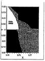
도 13c 및 13d는 각각 예1에 설명된 것과 같은, 도 10a 및 10b의 게이트 전극들의 드레인 에지에서의 2차원 전기장 시뮬레이션.13C and 13D are two-dimensional electric field simulations at the drain edges of the gate electrodes of FIGS. 10A and 10B, respectively, as described in Example 1. FIGS.
도 14는 예2에 설명된 장치에 대하여 드레인 누설 전류를 드레인-소스 전압의 함수로서 나타내는 도면.FIG. 14 shows the drain leakage current as a function of drain-source voltage for the apparatus described in Example 2. FIG.
도 15는 본 발명의 일 실시예에 따른, 부동태층의 두께보다 얇은 게이트 전극 높이를 포함하는 질화갈륨 재료 장치의 단면도.15 is a cross-sectional view of a gallium nitride material device including a gate electrode height thinner than the thickness of a passivation layer, in accordance with an embodiment of the present invention.
본 발명은 질화갈륨 재료 장치 및 그 형성 방법을 제공한다. 이 장치는 전극 형성층을 포함한다. 전극 형성층은 전형적으로 그 내부에 (적어도 부분적으로) 전극이 형성된 비아를 갖는다. 따라서, 비아는 (적어도 부분적으로) 전극의 치수를 정의한다. 몇몇 경우에, 전극 형성층은 질화갈륨 재료 영역 상에 형성된 부동태층이다.The present invention provides a gallium nitride material device and a method of forming the same. The apparatus includes an electrode forming layer. The electrode forming layer typically has vias (at least partially) with electrodes formed therein. Thus, the via defines (at least partially) the dimensions of the electrode. In some cases, the electrode forming layer is a passivation layer formed on the gallium nitride material region.
도 1a 및 1b는 본 발명의 일 실시예에 따른 질화갈륨 재료 영역(12)을 포함하는 반도체 장치(10)를 나타낸다. 나타낸 실시예에서, 장치(10)는 질화갈륨 재료 영역 상에 형성된 소스 전극(14), 드레인 전극(16) 및 게이트 전극(18)을 포함하는 FET(field effect transistor)이다. 질화갈륨 재료 영역은 기판(20) 상에 형성되 며, 나타낸 바와 같이, 전이층(22)은 기판과 질화갈륨 재료 영역 사이에 형성될 수 있다. 나타낸 바와 같이, 장치는 질화갈륨 재료 영역의 표면을 보호하고 부동태화하는 부동태층(passivating layer)인 전극 형성층(24)을 포함한다. 비아(26)는 부분적으로 층(24) 내에 형성되고, 그 내부에 게이트 전극이 형성된다. 후술된 바와 같이, 비아의 모양 및 크기는, 그리고 그에 따른 게이트 전극의 모양 및 크기는, 장치의 속성을 향상시키도록 제어될 수 있다.1A and 1B show a
도 1a 및 1b에 나타낸 실시예에서는 장치(10)가 FET이지만, 후술된 것과 같이 본 발명은 다른 유형의 장치들도 포함한다. 본 발명의 FET가 사용되지 않는 실시예에서, 전극 형성층은 게이트 전극 이외의 쇼트키 컨택트 등의 다른 유형의 전극을 형성할 수 있다는 것이 이해되어야 한다. 또한, 도 1a 및 1b 내의 전극 형성층은 부동태층으로서 동작하지만, 다른 실시예에서, 전극 형성층은 부동태층으로서 동작하지 않을 수도 있다(예를 들어, 도 4 참조).Although the
층이 다른 층 또는 기판 "상에(on)" 또는 "위에(over)" 있다고 언급될 때, 그것은 층 또는 기판 상에 바로 위치하는 것일 수 있으며, 또는 매개층이 또한 존재할 수도 있다. 다른 층 또는 기판 "바로 위에" 있는 층은 매개층에 없다는 것을 의미한다. 또한 층이 다른 층 또는 기판 "상에" 또는 "위에" 있다고 언급될 때, 그것은 층이나 기판 전체, 또는 층이나 기판의 일부분을 덮을 수 있다는 것도 이해되어야 한다.When a layer is referred to as being "on" or "over" another layer or substrate, it may be located directly on the layer or substrate, or an intermediate layer may also be present. It is meant that no other layer or layer "on top" of the substrate is in the intermediate layer. It is also to be understood that when a layer is referred to as "on" or "on" another layer or substrate, it may cover the layer or the substrate as a whole, or a portion of the layer or substrate.
여기에 사용된 바와 같이, "부동태층"이란 용어는 하지층(예를 들어, 질화갈륨 재료 장치(12)) 상에 성장되면, 하지층의 밴드갭 내의 표면/계면 준위의 개수를 줄이고, 및/또는 그것의 성분을 보호하거나, 하지층의 표면/계면에서의 자유 캐리어(예를 들어, 전극 또는 홀) 트랩핑 준위(free carrier trapping state)의 개수를 줄이고, 및/또는 그것의 성분을 보호하는 임의의 층을 의미한다. 예를 들어, 트랩핑 준위는 종결되지 않은 화학적 결합에 의해 생성되는 표면 준위에 관련되어, 주위 환경으로부터 표면에 흡수된 이온 또는 표면에서의 전위(dislocation)를 스레딩(threading)할 수 있게 된다. FET 장치에서, 트랩핑 준위는 자유 캐리어를 캡처하고 DC 또는 RF 동작 동안 바람직하지 않은 공핍 영역을 생성할 수 있다. 이러한 영향은 그것이 없었다면 동작하는 동안 FET의 채널 내에서 흘렀을 전류의 양을 줄일 수 있으며, 따라서 장치의 성능을 약화시킬 수 있다. 부동태층은 이러한 영향을 상당히 줄임으로써, 향상된 출력 전력 또는 효율 등의 장치의 전기적 성능을 향상시킬 수 있다. 부동태층은 또한 장치의 항복 전압을 증가시킬 수 있다.As used herein, the term " passive layer ", when grown on an underlayer (e.g., gallium nitride material device 12), reduces the number of surface / interface levels in the bandgap of the underlayer, and And / or protect its components, reduce the number of free carrier trapping states (eg electrodes or holes) at the surface / interface of the underlying layer, and / or protect its components It means any layer. For example, trapping levels relate to surface levels created by unterminated chemical bonds, thereby allowing threading of ions or dislocations at the surface absorbed by the surface from the surrounding environment. In FET devices, trapping levels can capture free carriers and create undesirable depletion regions during DC or RF operation. This effect can reduce the amount of current that would otherwise flow in the channel of the FET during operation, and thus degrade the performance of the device. The passivation layer significantly reduces this effect, thereby improving the electrical performance of the device, such as improved output power or efficiency. The passivation layer can also increase the breakdown voltage of the device.
부동태층은 또한 포토리소그래픽, 에칭, 금속(예를 들어, 게이트, 상호접속) 퇴적, 주입, 습식 화학, 및 레지스트 스트립(예를 들어, 플라즈마 내의) 단계들을 포함하는 후속 프로세스 단계들 동안 하지층(예를 들어, 질화갈륨 재료 장치(12))을 보호할 수 있다는 것이 이해되어야 한다. 따라서, 부동태층은 다른 프로세스 종류(예를 들어, 액체, 이온, 플라즈마, 가스 종류)가 질화갈륨 재료의 표면과 반응 및/또는 상호작용하는 것을 제한 또는 제거할 수 있다. 이러한 반응 및/또는 상호작용은 표면 형태학, 표면 준위 개수, 표면 전하의 양, 표면 전하의 극성 또는 이들의 임의의 조합을 변경시킴으로써 장치의 전기적 속성에 불리해질 수 있다.The passivation layer also underlies the underlying layer during subsequent process steps, including photolithography, etching, metal (eg, gate, interconnect) deposition, implantation, wet chemistry, and resist strip (eg, within plasma) steps. It should be understood that it is possible to protect (eg, gallium nitride material device 12). Thus, the passivation layer may limit or eliminate the reaction and / or interaction of other process types (eg, liquid, ionic, plasma, gas types) with the surface of the gallium nitride material. Such reactions and / or interactions may be detrimental to the electrical properties of the device by altering surface morphology, number of surface levels, amount of surface charge, polarity of surface charge, or any combination thereof.
전극 형성층(24)의 적절한 성분은 질화물 기반 화합물(예를 들어, 질화실리 콘 화합물), 산화물 기반 화합물(예를 들어, 산화실리콘 화합물), 폴리이미드(polyimide), 다른 비전기적 재료, 또는 이러한 성분들의 조합(예를 들어, 산화실리콘과 질화실리콘)을 포함하지만, 이에만 한정되는 것은 아니다. 몇몇의 경우에는, 전극 형성층이 질화실리콘 화합물(예를 들어, Si3N4) 또는 비화학량론(non-stoichiometric) 질화실리콘 화합물인 것이 바람직할 수 있다. 이러한 성분은, 전극 형성층이 부동태층으로 기능하거나(도 1a 및 1b에 도시된 바와 같음), 전극 형성층이 부동태층으로 기능하지 않을 때 적절하다는 것이 이해되어야 한다.Suitable components of
전극 형성층(24)의 두께는 장치의 설계에 따른다. 몇몇 경우, 전극 형성층은 약 50 옹스트롬 내지 1.0 미크론 사이의 두께를 가질 수 있다. 몇몇 경우에는 두께가 약 700 옹스트롬 내지 약 1200 옹스트롬 사이일 수도 있다.The thickness of the
나타낸 바와 같이, 전극 형성층(24)은 전극 영역(소스(14), 드레인(16) 및 게이트(18))을 제외한 질화갈륨 재료 영역(12)의 표면 전체를 덮는다.As shown, the
도 1-2에서, 중요한 치수를 나타내기 위해 다음의 지정들이 사용된다: 게이트 길이(즉, 비아의 하단에서의 게이트의 단면 치수)(a), 비아의 상단에서의 단면 치수(b), 전극 형성층 두께(c), 소스 전극측 돌출 거리(d), 드레인 전극측 돌출 거리(e), 게이트-소스 간격(f), 게이트-드레인 간격(g) 및 게이트 전극 높이(h).In Figures 1-2, the following designations are used to indicate important dimensions: gate length (i.e. cross-sectional dimension of the gate at the bottom of the via) (a), cross-sectional dimension (b) at the top of the via, electrode Formation layer thickness (c), source electrode side protrusion distance (d), drain electrode side protrusion distance (e), gate-source spacing (f), gate-drain spacing (g) and gate electrode height (h).
상기 언급된 단면적은 소스 및 드레인 전극에 수직인 평면 P(도 1b) 내에서 측정된 것이며, 그들 간의 최소 거리를 정의한다.The cross-sectional area mentioned above is measured in plane P (FIG. 1B) perpendicular to the source and drain electrodes, and defines the minimum distance between them.
도 2는 비아 및 대응하는 게이트 전극의 프로파일을 나타낸다. 각 Z는 전극 형성층의 측벽(28)이 전극 형성층의 저면(30)으로부터 위쪽으로 연장된 각이고, 각 Y는 측벽이 전극 형성층의 상단면(32)으로부터 아래쪽으로 연장된 각이다. 각 Y 및 Z는 각각 저면(30) 및 상단면(32)에서 측정되며, 측벽(28)은 저면 및 상단면으로부터 떨어져 있는 곳에서 이러한 각들에서 빗나갈 수 있다.2 shows a profile of a via and a corresponding gate electrode. Each Z is an angle in which the
전술된 치수 및 각은 도 1 및 2의 FET 실시예들의 게이트 전극에 관련하여 나타내져있지만, 이러한 치수 및 각 중에서 몇몇은 또한 후술된 바와 같은 FET를 사용하지 않는 실시예들의 다른 유형의 전극에도 적용될 수 있다.Although the dimensions and angles described above are shown in relation to the gate electrodes of the FET embodiments of FIGS. 1 and 2, some of these dimensions and angles may also be applied to other types of electrodes of embodiments that do not use a FET as described below. Can be.
유리하게도, 후술된 본 발명의 장치 형성 방법은 게이트 전극 치수(예를 들어, a)가 전체적으로 전극 형성층 내에 형성되는 것을 허용한다. 이것은 전극 형성층 퇴적 이전에 게이트 전극을 형성하는 프로세스, 또는 게이트 길이(a)가 아니라 게이트 전극 일부분을 전극 형성층 내에 형성하는 프로세스와는 구별된다. 예를 들어, 전극 형성층 내에 게이트 전극의 일부분을 정의하는 이러한 프로세스는 게이트 전극 재료로 완벽하게 채워지지 않는 영역(예를 들어, 전극 형성층을 언더컷(undercut)한 저면(30)에 인접한 영역)을 비아 내에 포함할 수 있다. 이러한 프로세스에서, 게이트 길이는 이에 따라 완전히 전극 형성층에 의해서만 정의되지 못할 수 있다. 반대로, 소정의 바람직한 본 발명의 방법에서, 비아 전체가 게이트 전극 재료로 채워져, 비아의 치수가 게이트 치수, 특히 게이트 길이에 정확하게 대응하게 된다. 따라서, 본 발명의 방법을 이용하면, 중요한 전극 치수(예를 들어, 게이트 길이)는 장치 성능을 최적화하도록 정확하게 제어될 수 있다. 본 발명의 일 양태는 어떠한 게이트 전극 치수(게이트 전극 프로파일 포함)가 FET 장치(10) 내의 성능 향상을 이끌어낼 수 있다는 것을 개시한다.Advantageously, the device formation method of the present invention described below allows the gate electrode dimension (e.g., a) to be formed entirely in the electrode formation layer. This is distinct from the process of forming the gate electrode prior to the electrode formation layer deposition, or the process of forming a portion of the gate electrode in the electrode formation layer rather than the gate length a. For example, this process of defining a portion of the gate electrode in the electrode forming layer may via a region that is not completely filled with the gate electrode material (eg, an area adjacent the bottom 30 that undercut the electrode forming layer). It can be included within. In this process, the gate length may thus not be fully defined only by the electrode forming layer. In contrast, in certain preferred methods of the present invention, the entire via is filled with the gate electrode material such that the dimensions of the via correspond exactly to the gate dimensions, in particular the gate length. Thus, using the method of the present invention, important electrode dimensions (eg, gate length) can be precisely controlled to optimize device performance. One aspect of the present invention discloses that any gate electrode dimension (including gate electrode profile) can lead to performance improvements within the
본 발명의 몇몇 방법에서, 게이트 전극 높이(h)가 전극 형성층 두께(c)보다 작으면(도 15 참조), 상단면(32)에서의 또는 그에 인접한 비아의 영역은 게이트 전극 재료로 채워지지 않을 수 있다는 것이 이해되어야 한다.In some methods of the invention, if the gate electrode height h is less than the electrode forming layer thickness c (see FIG. 15), the region of the via at or adjacent the
도 1a 및 1b에 나타낸 실시예에서, 게이트 길이(a)는 비아의 상단에서의 단면 치수(b)보다 작다. 비아(26)(따라서, 게이트 전극(18))는 또한 비아의 하단에서의 단면적보다 넓은 비아의 상단에서의 단면적을 갖는다. 나타낸 바와 같이, 비아(따라서, 게이트 전극(18))의 단면적은 비아의 상단에서 비아의 하단으로 갈수록 작아진다. 측벽(28)은 곧은(굽지 않은) 경사를 갖는 것이 바람직할 수 있다. 몇몇 경우에는, 측벽(28)이 굽은 경사를 갖는 것이 바람직할 수도 있다. 측벽이 굽은 경사를 갖는 경우, 나타낸 바와 같이 측벽은 질화갈륨 재료 영역(12)에 대하여 위로 오목한(concave-up) 모양을 가질 수 있다. 후술된 바와 같이, 전극 형성층 에칭 단계는 원하는 게이트 프로파일을 제공하도록 제어될 수 있다.In the embodiment shown in FIGS. 1A and 1B, the gate length a is smaller than the cross-sectional dimension b at the top of the via. Via 26 (thus gate electrode 18) also has a cross sectional area at the top of the via that is wider than the cross sectional area at the bottom of the via. As shown, the cross-sectional area of the via (and hence gate electrode 18) becomes smaller from the top of the via to the bottom of the via. It may be desirable for
비아(및 전극)의 단면적은 나타낸 전극 형성층에 의해 형성된 평면에 평행한 평면에서 측정된다는 것이 이해되어야 한다.It should be understood that the cross-sectional area of the via (and electrode) is measured in a plane parallel to the plane formed by the electrode forming layer shown.
(a)/(b)의 비율이 항복 전압에 영향을 주는, 장치(10)에 대한 중요한 설계 매개변수일 수 있다는 것은 알려져 있다. 본 발명의 몇몇 실시예에서, (a)/(b)의 비율은 약 0.50 내지 약 0.95 사이가 되도록 제어된다. 몇몇 경우에서는, 비율을 약 0.75 내지 0.90이 되도록 제어하는 것이 바람직할 수도 있다. 이러한 범위 내의 (a)/(b) 비율 값은 항복 전압을 향상시킬 수 있다. (a)/(b) 비율의 최적 값은 특정한 장치에 따라 달라지며, 또한 다른 설계 매개변수에 따라 달라질 수도 있다. 후술된 바와 같이, 전극 형성층 에칭 단계의 매개변수는 원하는 (a)/(b) 비율을 제공하도록 제어될 수 있다.It is known that the ratio of (a) / (b) may be an important design parameter for
게이트 길이 (a)의 절대값은 특정한 장치 설계에 따른다. 예를 들어, (a)는 약 0.1 미크론 내지 약 5.0 미크론 사이일 수 있다. 그러나, (a)에 대한 다른 값들도 또한 적절할 수 있음이 이해되어야 한다.The absolute value of the gate length (a) depends on the particular device design. For example, (a) can be between about 0.1 micron and about 5.0 micron. However, it should be understood that other values for (a) may also be appropriate.
또한 각 Y 및 Z가 장치 동작에 대하여 바람직한 범위를 갖는다는 것도 알려져 있다. 각 Z는 90도 미만인 것이 바람직할 수 있다. 예를 들어, 각 Z는 약 5도 내지 약 85 사이가 바람직할 수 있지만, 몇몇 경우에는 약 10도 내지 약 60도 사이, 그리고 몇몇 경우에는 약 15도 내지 약 40도 사이가 바람직할 수 있다. 각 Y는 90도 초과인 것이 바람직할 수 있다. 각 Y는 전형적으로 약 90도 내지 약 160도 사이이다. 각 Y는 약 90도 내지 약 135도 사이인 것이 바람직하지만, 몇몇 경우에는 약 90도 내지 약 110도 사이인 것이 바람직할 수 있다.It is also known that each Y and Z has a preferred range for device operation. It may be desirable for each Z to be less than 90 degrees. For example, each Z may preferably be between about 5 degrees and about 85 degrees, but in some cases between about 10 degrees and about 60 degrees, and in some cases between about 15 degrees and about 40 degrees. It may be desirable for each Y to be greater than 90 degrees. Each Y is typically between about 90 degrees and about 160 degrees. Each Y is preferably between about 90 degrees and about 135 degrees, but in some cases it may be preferred between about 90 degrees and about 110 degrees.
각 Y 및 Z가 장치에 의해 형성된 전기장의 위치 및 세기에 영향을 준다고 판정되어 왔다. Y 및 Z의 값을 상기 범위 내로 제어함으로써, 장치 동작 동안 게이트 전극의 드레인 에지(drain edge)에 인접하게 생성되는 최고 전기장이 감소될 수 있다. 이러한 개선은 동작 전압을 증가시키고 및/또는 게이트 누설 전류를 감소시킬 수 있다. Y 및 Z의 값이 상기 범위 이외의 값이면, 게이트 전극의 드레인 에지에 인접하게 생성된 최고 전기장이 너무 높아, 초과 게이트 누설 전류 및/또는 조기 장치 실패를 발생시킬 수 있다.It has been determined that each Y and Z affects the position and intensity of the electric field formed by the device. By controlling the values of Y and Z within this range, the highest electric field generated adjacent to the drain edge of the gate electrode during device operation can be reduced. This improvement may increase operating voltage and / or reduce gate leakage current. If the values of Y and Z are outside the above ranges, the highest electric field generated near the drain edge of the gate electrode is too high, which may cause excess gate leakage current and / or premature device failure.
전술된 각 Y 및 Z의 범위는 또한 게이트 전극 재료로 비아를 완벽하게 채우게 하는데 중요하다. 각 Y 및 Z의 최적 값(들)은 특정한 장치에 따르며, 또한 다른 설계 매개변수에 따를 수도 있다. 후술된 바와 같이, 전극 형성층 에칭 단계는 각 Y 및 Z의 원하는 값을 제공하도록 제어될 수 있다.The range of angles Y and Z described above is also important to fully fill the via with the gate electrode material. The optimal value (s) of each Y and Z depends on the particular device and may also depend on other design parameters. As described below, the electrode forming layer etching step can be controlled to provide the desired values of each Y and Z.
후술된 바와 같이, 각 Y 및 Z은 또한 FET 장치를 사용하지 않는 쇼트키 다이오드(예를 들어, 도 5의 (a) 및 (b) 참조)에 중요할 수 있다.As described below, each Y and Z may also be important for Schottky diodes (eg, see FIGS. 5A and 5B) that do not use a FET device.
여기서 언급된 각들은 예를 들어, (도 13a에 나타낸 바와 같이) SEM을 사용하여 현미경 스케일(예를 들어, 약 50 또는 100 옹스트롬보다 큰 치수)로 측정될 수 있다는 것이 이해되어야 한다. 각은 예를 들어 TEM을 사용하여 각의 값을 왜곡시킬 수 있는 존재 표면 효과(예를 들어, 원자의 단층)를 나타내는 원자 스케일로 측정되도록 의도되지 않는다.It should be understood that the angles referred to herein can be measured on a microscope scale (eg, dimensions greater than about 50 or 100 angstroms) using, for example, an SEM (as shown in FIG. 13A). The angles are not intended to be measured on an atomic scale that exhibits an existing surface effect (eg, a monolayer of atoms) that can distort the value of the angle using, for example, a TEM.
또한 게이트 전극은 하지 전극 형성층(24) 위로 돌출된 일부분을 포함하는 T자형 설계를 갖는 것도 바람직하다. 장치의 항복 전압을 생성하는데 드레인 전극측 돌출 거리(e)가 특히 중요하다고 판정됐다. 드레인 전극의 방향에서 전극 형성층 위로 돌출된 게이트 전극의 일부분은 (다른 유용한 효과들 중에서) 장치의 항복 전압을 증가시키는 필드 플레이트(field plate)로 기능할 수 있다. 예를 들어, (e)가 게이트 드레인 간격(g)의 약 2 퍼센트 내지 약 60 퍼센트 사이일 때, 항복 전압은 증가할 수 있음이 알려져 있다. 몇몇의 경우, 장치의 항복 전압을 더욱 최적화하기 위해 (e)는 약 10 퍼센트 내지 약 50 퍼센트 사이인 것이 바람직할 수 있다. (e)의 최적 값(들)은 특정한 장치에 따라 달라지며, 또한 다른 설계 매개변수 에 따라 달라질 수도 있다.It is also desirable for the gate electrode to have a T-shaped design that includes a portion that projects above the underlying
소스 전극측 돌출 거리(d)를 드레인 전극측 돌출 거리(e)보다 짧도록 제어하는 것이 이롭다는 것도 또한 알려져 있다. 몇몇 경우에, (d)는 (e)의 50 퍼센트보다 짧거나, 심지어는 (e)의 20%보다 짧은 것이 바람직하다. 몇몇 경우에는, 비아 전체가 채워질 것을 보장하는 한편, (d)를 최소화하는 것이 이롭다. (d)의 값을 줄이는 것은 원하지 않는 게이트-소스 용량을 제한 또는 방지한다.It is also known that it is advantageous to control the source electrode side protrusion distance d to be shorter than the drain electrode side protrusion distance e. In some cases, it is preferred that (d) is shorter than 50 percent of (e) or even shorter than 20 percent of (e). In some cases it is beneficial to minimize (d) while ensuring that the entire via is filled. Reducing the value of (d) limits or prevents unwanted gate-source capacity.
(d) 및 (e)의 값은 부분적으로 후술되는 패터닝 단계 및 금속 퇴적에 의해 제어된다.The values of (d) and (e) are controlled in part by the patterning step and metal deposition described below.
소스 전극측 돌출 거리(d), 드레인 전극측 돌출 거리(e), 게이트 소스 간격(f) 및 게이트 드레인 거리(g)의 절대값은 장치 설계에 따른다. 비록 다른 값들도 가능하지만, 전형적인 (f) 및 (g) 값은 약 0.1 미크론 내지 약 10 미크론 사이이다.The absolute values of the source electrode side protrusion distance d, the drain electrode side protrusion distance e, the gate source spacing f and the gate drain distance g depend on the device design. Although other values are possible, typical values of (f) and (g) are between about 0.1 micron and about 10 microns.
몇몇 실시예에서, 게이트 전극 높이(h)의 값은 전극 형성층 두께(c)의 값보다 크다(도 1a 참조). 다른 실시예에서, 게이트 전극 높이(h)의 값은 전극 형성층 두께(c)의 값보다 작다(도 15 참조). 다른 게이트 치수들만큼 중요하진 않지만, (h)의 바람직한 값은 특정한 장치에 따르며, 또한 다른 설계 매개변수에 따를 수도 있다. 예를 들어, (h)는 약 100 옹스트롬 내지 2.0 미크론 사이일 수 있다. (h) 값은 후술된 바와 같은 게이트 전극 재료를 퇴적시키는데 사용되는 프로세싱 조건에 의해 제어될 수 있다.In some embodiments, the value of the gate electrode height h is greater than the value of the electrode forming layer thickness c (see FIG. 1A). In another embodiment, the value of the gate electrode height h is smaller than the value of the electrode formation layer thickness c (see FIG. 15). Although not as important as other gate dimensions, the preferred value of (h) depends on the particular device and may also depend on other design parameters. For example, (h) may be between about 100 angstroms and 2.0 microns. The value (h) can be controlled by the processing conditions used to deposit the gate electrode material as described below.
게이트 전극(18)은 금속(예를 들어, Au, Ni), 금속 화합물(예를 들어, WSi, WSiN), 합금, 반도체, 폴리실리콘, 질화물 또는 이들 재료의 조합물 등의 임의의 적절한 도전성 금속으로 형성될 수 있다. 예를 들어, 게이트 전극은 금, 니켈 또는 둘 모두로 형성될 수 있다. 유익하게도, 비아(26) 내에 게이트 전극을 형성함으로써 게이트 길이 전체에 걸쳐 질화갈륨 금속 영역에 바로 접촉하여 단일 도전성 금속 성분(예를 들어, 니켈)을 포함하는 게이트 전극을 형성할 수 있으며, 게이트 전극이 제2 도전성 금속 성분도 포함하는 경우에도 그러하다. 예를 들어, 게이트 전극이 니켈 및 금으로 형성될 때, 니켈층은 게이트 길이 전체에 걸쳐 질화갈륨 재료 영역에 바로 접촉해 있을 수 있으며, 금층이 니켈층 위에 형성될 수 있다(도 13a 참조). 반대로, 복수의 금속 성분을 포함하는 게이트 전극을 형성하기 위한 종래 기술은 게이트 길이의 내부에 바로 접촉해 있는 제1 성분(예를 들어, 니켈) 및 게이트 길이의 에지부에 바로 접촉해 있는 제2 성분(예를 들어, 금)을 포함할 수 있다(도 13b 참조). 게이트 길이 전체에 걸쳐 질화갈륨 재료 영역에 바로 접촉하여 단일 성분을 제공하는 것은 제2 성분이 게이트 길이의 일부분들에 바로 접촉해 있을 때 발생할 수 있는 손실을 제거함으로써 게이트 누설 전류를 줄이는 등의 전기적 속성을 향상시킬 수 있다. 또한, 복수의 성분들이 질화갈륨 재료 영역에 바로 접촉해 있을 때는, 게이트 전극의 쇼트키 장벽 높이가 금속 성분에 의해 제어될 수 없을 수 있다.
또한 소스 전극(14) 및 드레인 전극(16)은 Ti, Al, Pt 또는 Si뿐만 아니라 게이트 전극에 관련하여 전술된 것과 동일한 금속을 포함하는 임의의 적절한 도전성 재료로 형성될 수도 있다.The
어떤 바람직한 실시예에서, 기판(20)은 실리콘 기판이다. 여기에 사용된 바와 같이, 실리콘 기판은 실리콘면을 포함하는 임의의 기판을 의미한다. 적절한 실리콘 기판의 예는 다른 것들 중에서 전체적으로 실리콘으로만 구성된 기판(예를 들어, 벌크 실리콘 웨이퍼(bulk silicon wafer)), SOI(sillicon-on-insulator) 기판, SOS(silicon-on-sapphire) 기판 및 SIMOX 기판을 포함한다. 적절한 실리콘 기판은 또한 다이아몬드, AIN 또는 다른 다결정 재료 등의 또 다른 재료에 본딩(bonding)되된 실리콘 웨이퍼를 갖는 기판을 포함한다. 다른 결정학적 방향을 갖는 실리콘 기판이 사용될 수도 있다. 몇몇 경우에는 실리콘(111) 기판이 바람직하다. 다른 경우에는 실리콘(100) 기판이 바람직하다.In some preferred embodiments, the
사파이어, 탄화실리콘, 질화갈륨 및 질화알루미늄 기판을 포함하는 다른 유형의 기판들도 사용될 수 있음이 이해되어야 한다.It should be understood that other types of substrates may be used, including sapphire, silicon carbide, gallium nitride, and aluminum nitride substrates.
기판(20)은 임의의 적절한 치수를 가질 수 있으며, 그것의 특정한 치수는 응용에 따라 지시된다. 2인치(50mm), 4인치(100mm), 6인치(150mm) 및 8인치(200mm)가 적절한 지름이지만, 이에만 한정되는 것은 아니다. 몇몇 실시예에서, 기판(20)은 예를 들어 250 미크론보다 상대적으로 두껍다. 보다 두꺼운 기판은 일반적으로 얇은 기판에서 몇몇 경우에 발생할 수 있는 휨(bending)을 방지할 수 있다. 다른 실시예에서는 보다 얇은 기판(예를 들어, 250 미크론보다 얇음)이 사용된다.
전이층(22)은 질화갈륨 재료 영역(12)이 퇴적되기 전에 기판(20) 상에 형성될 수 있다. 전이층은 다음 중 하나 이상을 수행할 수 있다: 질화갈륨 재료와 기판 간의 열팽창율 차로부터 발생되는 열 스트레스를 낮춤으로써 질화갈륨 재료 영 역(12) 내의 균열(crack) 형성을 줄이는 것; 질화갈륨 재료와 기판 간의 격자상수 차로부터 발생되는 격자 스트레스를 낮춤으로써 질화갈륨 재료 영역 내의 결함 형성을 줄이는 것; 및 기판과 질화갈륨 재료 간의 밴드 갭 차를 줄임으로써 기판과 질화갈륨 재료 영역 간의 도전성을 증가시키는 것. 질화갈륨 재료와 실리콘 간의 열팽창율과 격자상수에의 큰 차이 때문에, 실리콘 기판을 사용할 때 전이층이 존재하는 것이 특히나 바람직할 수 있다. 다양한 이유로 전이층은 또한 기판(20)과 질화갈륨 재료 영역 사이에 형성될 수 있음이 이해되어야 한다. 몇몇 경우에, 예를 들어, 실리콘 기판이 사용되지 않는 경우, 장치는 전이층을 포함하지 않을 수 있다.The
전이층(22)의 성분은 적어도 부분적으로 기판의 유형 및 질화갈륨 재료 영역(12)의 성분에 따른다. 실리콘 기판을 사용하는 몇몇 실시예에서, 전이층은 층의 적어도 일부분에 걸쳐 다양한 성분을 갖는 조성-기울기를 갖는 전이층(compositionally-graded transition layer)을 포함하는 것이 바람직할 수 있다. 적절한 조성-기울기를 갖는 전이층은, 예를 들어 여기에 참조에 의해 통합된 미국특허번호 제6,649,287의 "Gallium Nitride Materials and Methods"(2000년 12월 14일)에 설명되어 있다. 조성-기울기를 갖는 전이층은 특히 질화갈륨 재료와 기판(예를 들어, 실리콘) 간의 열팽창율 차로부터 발생하는 열 스트레스를 줄임으로써 질화갈륨 재료 영역 내의 균열 형성을 줄이는데 효과적이다. 몇몇 실시예에서, 조성-기울기를 갖는 전이층은 AlxInyGa(1-x-y)N, AlxGa(1-x)N 또는 InyGa(1-y)N 등의 질화갈 륨의 합금으로 형성되며, 여기서 0≤x≤1, 0≤y≤1이다. 이러한 실시예에서, 합금의 요소(예를 들어, Ga, Al, In) 중 적어도 하나의 농도는 전형적으로 층의 단면 두께의 적어도 일부분에 걸쳐 다양하다. 몇몇 경우, 전이층은 단일결정 구조를 갖는다.The composition of the
다른 실시예에서, 전이층(22)은 그것의 두께에 걸쳐 일정한(즉, 다양하지 않은) 성분을 갖는다. 이러한 전이층은 또한 버퍼층으로 언급될 수도 있다.In other embodiments, the
몇몇 실시예에서, 장치(10)는 또한 도면에 나타내지 않은 다른 층들도 선택적으로 포함할 수 있다. 예를 들어, 장치(10)는 하나 이상의 중간층을 포함할 수 있다. 예를 들어, 중간층은 기판과 전이층(예를 들어, 조성-기울기를 갖는 전이층) 사이에 및/또는 전이층과 질화갈륨 재료 영역 사이에 형성될 수 있다. 예를 들어, 적절한 중간층은 상기 참조에 의해 통합된 미국특허번호 제6,649,287호에 설명 및 나타나있다. 몇몇 실시예에서, 중간층은 질화갈륨 합금(AlxInyGa(1-x-y)N,AlxGa(1-x)N 또는 InyGa(1-y)N 등)의 일정한 성분, 질화알루미늄 또는 질화알루미늄 합금을 가질 수 있다. 몇몇 경우에, 중간층(들)은 단일결정 구조를 갖는다.In some embodiments,
질화갈륨 재료 영역(12)은 적어도 하나의 질화갈륨 재료 층을 포함한다. 여기에 사용된 바와 같이, "질화갈륨 재료"란 구문은 질화갈륨(GaN) 및 다른 것들 중에서 AlxGa(1-x)N, InyGa(1-y)N, AlxInyGa(1-x-y)N, GaAsaPbN(1-a-b), AlxInyGa(1-x-y)AsaPbN(1-a-b) 등의 임의의 합금을 의미한다. 전형적으로, 비소 및/또는 인이 존재할 경우, 그들은 농도가 낮다(즉, 5 무게 퍼센트 미만). 어떤 바람직한 실시예에서, 질화갈륨 재료는 고농도의 갈륨을 가지며, 알루미늄 및/또는 인듐을 거의 포함하지 않거나 아예 포함하지 않는다. 고농도 갈륨의 실시예에서, (x+y)의 합은 0.4 미만이거나, 0.2 미만이거나, 0.1 미만이거나, 심지어는 그 미만일 수 있다. 몇몇 경우에서, 질화갈륨 재료 층은 GaN 성분을 갖는 것이 바람직하다(즉, x+y=0). 질화갈륨 재료는 n형 또는 p형 도핑(dopping)될 수 있거나, 진성(intrinsic)일 수 있다. 적절한 질화갈륨 재료는 상기 참조에 의해 통합된 미국특허번호 제6,649,287호에 설명되어 있다.Gallium
몇몇 경우에, 질화갈륨 재료 영역(12)은 오직 하나의 질화갈륨 재료 층만을 포함한다. 다른 경우에, 질화갈륨 재료 영역(12)은 2개 이상의 질화갈륨 재료 층을 포함한다. 상이한 층들은 반도체 장치의 상이한 영역을 형성할 수 있다. 질화갈륨 재료 영역(12)은 또한 다른 Ⅲ-Ⅴ족 화합물 또는 합금, 산화층 및 금속층 등의 질화갈륨 재료 성분을 갖지 않는 하나 이상의 층을 포함할 수도 있다.In some cases, gallium
질화갈륨 재료 영역(12)은 그것 내에 장치의 형성을 허용하기에 충분히 품질이 높다. 가급적 질화갈륨 재료 영역(12)은 낮은 균열 레벨 및 낮은 결함 레벨을 갖는다. 전술된 바와 같이, 전이층(22)(특히 조성-기울기를 갖는 것일 경우)은 균열 및/또는 결함 형성을 줄일 수 있다. 몇몇 실시예에서, 질화갈륨 재료 영역은 약 109결함/cm2를 갖는다. 낮은 균열 레벨을 갖는 질화갈륨 재료는 상기 참조에 의해 통합된 미국특허번호 제6,649,287호에 설명되어 있다. 몇몇 경우, 질화갈륨 재료 영역은 0.005㎛/㎛2 미만의 균열 레벨을 갖는다. 몇몇 경우, 질화갈륨 재료 영 역은 0.001㎛/㎛2 미만의 매우 낮은 균열 레벨을 갖는다. 특정한 경우에, 질화갈륨 재료 영역은 0.0001㎛/㎛2 미만의 균열 레벨로 정의된 바와 같이 실제로 균열이 없는 것이 바람직할 수 있다.The gallium
어떤 경우, 질화갈륨 재료 영역(12)은 단일결정 구조를 갖는 층 또는 층들을 포함한다. 몇몇 경우, 질화갈륨 재료 영역은 우르짜이트(Wurtzite)(육방정계) 구조를 갖는 하나 이상의 층들을 포함한다.In some cases, gallium
질화갈륨 재료 영역(12)의 두께 및 다른 층들의 개수는 적어도 부분적으로 특정한 장치의 요구사항에 의해 지시된다. 최소한, 질화갈륨 재료 영역(12)의 두께는 원하는 장치의 형성을 허용할만큼 충분하다. 항상 그런 것은 아니지만, 질화갈륨 재료 영역(12)은 일반적으로 0.1 미크론 이상의 두께를 갖는다. 다른 경우, 질화갈륨 재료 영역(12)은 0.5 미크론 이상의, 0.75 미크론 이상의, 0.1 미크론 이상의, 2.0 미크론 이상의, 또는 심지어 5.0 미크론 이상의 두께를 갖는다.The thickness of the gallium
도 3은 본 발명의 다른 실시예에 따른 반도체 장치(40)를 나타낸다. 도 3의 실시예에서, 비아(26)는 전극 형성층(24)의 두께를 통한 길의 일부분만으로 연장된다. 따라서, 전극 형성층 일부분은 게이트 전극(18)과 질화갈륨 재료 영역(12) 사이에 남아있다. 몇몇 실시예에서, 전극 형성층은 산화실리콘, 질화실리콘, 폴리이미드, 다른 유전체 재료 또는 이들 성분의 조합(예를 들어, 산화실리콘 및 질화실리콘) 등의 절연 재료로 형성되는 것이 바람직하다. 전극 형성층이 절연 재료로 형성되는 실시예에서, 장치(40)는 MISFET(metal-insulator-semiconductor)를 형성 한다.3 shows a
도 4는 본 발명의 다른 실시예에 따른 반도체 장치(42)를 나타낸다. 장치(42)는 전극 형성층(24)과 질화갈륨 재료 영역(12) 사이에 형성된 층(43)을 포함한다. 층(43)은 전극 형성층(24)과 다른 구조물을 갖는다. 몇몇 경우에, 층(43)은 부동태층인 것이 바람직하다. 적절한 부동태층 구성이 전술되었다. 몇몇 경우에는, 2개 이상의 층이 전극 형성층과 질화갈륨 재료 영역 사이에 형성될 수 있다는 것이 이해되어야 한다.4 shows a
도 5a 및 5b는 본 발명의 다른 실시예에 따른 반도체 장치(44)를 나타낸다. 이 실시예에서, 장치(44)는 비아(26) 내에 (부분적으로) 형성된 쇼트키 전극(46)(즉, 쇼트키 컨택트)을 포함하는 쇼트키 다이오드이다. 장치(44)는 또한 그 구조의 지름 둘레에 형성된 옴 전극(48)을 포함한다.5A and 5B show a semiconductor device 44 according to another embodiment of the present invention. In this embodiment, device 44 is a Schottky diode that includes a Schottky electrode 46 (ie, Schottky contact) formed (partially) in via 26. Device 44 also includes an
쇼트키 다이오드 실시예(또는 다른 장치)에서 FET 실시예에 관련하여 전술된 각 Y 및 Z의 범위도 또한 중요하다. 특히, 전술된 범위 내의 Y 및 Z의 값은, 다른 장점들 중에서 비아를 전극 재료로 완벽하게 채우는 것을 촉진시킨다. 각 Y 및 Z의 최적 값(들)은 특정한 장치에 따르며, 또한 다른 설계 매개변수에 따를 수 있다. 후술된 바와 같이, 전극 형성층 에칭 단계는 각 Y 및 Z의 원하는 값을 제공하도록 제어될 수 있다.The range of angles Y and Z described above with respect to the FET embodiment in the Schottky diode embodiment (or other device) is also important. In particular, the values of Y and Z within the aforementioned ranges facilitate the full filling of vias with electrode material, among other advantages. The optimal value (s) of each Y and Z depends on the particular device and may also depend on other design parameters. As described below, the electrode forming layer etching step can be controlled to provide the desired values of each Y and Z.
쇼트키 전극(46)은 또한, 도 1a 및 1b의 FET 실시예에 관련하여 설명된 바와 같이 하지 전극 형성층(24)에서 돌출된 일부분을 포함하는 T자형 설계를 갖는 것이 바람직할 수 있다. 돌출 거리(i)가 장치의 항복 전압에 영향을 주는데 특히 중요 하다고 결정됐다. 전극 형성층에서 옴 전극 방향으로 돌출된 쇼트키 전극의 일부분은 다른 유익한 효과들 중에서 장치의 항복 전압을 증가시키는 필드 플레이트로 기능할 수 있다. 예를 들어 (i)가 쇼트키 전극과 옴 전극 사이의 거리 (j)의 약 2퍼센트 내지 약 60퍼센트 사이일 때 항복 전압이 증가될 수 있다는 것이 알려져 있다. 몇몇 경우, 장치의 항복 전압을 더욱 최적화하기 위해 (i)는 (j)의 약 10 퍼센트 내지 약 50 퍼센트 사이인 것이 바람직할 수 있다. (j)의 최적 값(들)은 특정한 장치에 따르며, 또는 다른 설계 매개변수에 따를 수 있다.
본 발명의 쇼트키 다이오드는 또한 원이 아닌 레이아웃을 가질 수 있다는 것이 이해되어야 한다.It should be understood that the Schottky diode of the present invention may also have a layout other than a circle.
또한, 본 발명이 트랜지스터 및 쇼트키 다이오드에 관련하여 전술되었지만, 본 발명은 다른 장치들도 포함할 수 있다는 것이 이해되어야 한다. 예를 들어, 다른 전기 또는 전기광학 장치가 전극 형성층(몇몇 경우에 부동태층으로도 기능할 수 있음)을 사용할 수 있다. 적절한 장치는 쇼트키 정류기, 건 효과 다이오드(Gunn-effect diode), 버랙터 다이오드(varactor diode), 전압 제어 발진기, 광 방출 다이오드, 레이저 또는 광검출기를 포함한다.In addition, although the present invention has been described above with reference to transistors and Schottky diodes, it should be understood that the present invention may also include other devices. For example, other electro- or electro-optic devices may use an electrode forming layer (which in some cases may also function as a passivation layer). Suitable devices include Schottky rectifiers, Gunn-effect diodes, varactor diodes, voltage controlled oscillators, light emitting diodes, lasers or photodetectors.
도 6-11은 본 발명의 일 예시된 방법에 따른 상이한 프로세싱 단계 이후의 결과적인 반도체 구조물의 단면도를 나타낸다. 도 6-11이 본 발명의 일 방법에 따른 FET의 생성을 나타내지만, 유사한 방법 단계들을 사용하여 본 발명의 다른 장치들도 생성될 수 있다는 것도 또한 이해되어야 한다.6-11 illustrate cross-sectional views of the resulting semiconductor structure after different processing steps in accordance with one illustrated method of the present invention. 6-11 illustrate the creation of a FET in accordance with one method of the present invention, it should also be understood that other devices of the present invention may be created using similar method steps.
도 6은 기판(20) 상의 질화갈륨 재료 영역(12)과 전이층(22)의 퇴적, 및 소 스 전극(14)과 드레인 전극(16)의 퇴적 이후의 구조의 단면도를 나타낸다.6 shows a cross-sectional view of a structure after deposition of gallium
전이층(22) 및 질화갈륨 재료 영역(12)은 다른 기술들 중에서 예를 들어 MOCVD(metalorganic chemical vapor deposition), MBE(molecular beam epitaxy) 및 HVPE(hydride vapor phase epitaxy)를 사용하여 기판(20) 상에 퇴적될 수 있다. 소정의 경우에는, MOCVD 프로세스가 바람직할 수 있다. 실리콘 기판 위에 조성-기울기를 갖는 전이층 및 질화갈륨 재료 영역을 형성하기 위한 적절한 MOCVD 프로세스가 상기 참조에 의해 통합된 미국특허번호 제6,649,287호에 설명되어 있다. 질화갈륨 재료 영역(12)이 상이한 계층들을 가질 때, 몇몇 경우에는 단일 퇴적 단계(예를 들어, MOCVD 단계)를 사용하여 전체 영역(12)을 형성하는 것이 바람직할 수 있다. 단일 퇴적 단계를 사용할 때는, 상이한 층들을 형성하기 위해 프로세싱 매개변수가 알맞은 시간에 적절하게 바뀐다. 어떠한 바람직한 경우에는, 단일 성장 단계를 사용하여 전이층 및 질화갈륨 재료 영역이 형성될 수 있다.The
예를 들어, 참조에 의해 여기에 통합된 미국특허 번호 제6,051,849호에 설명된 바와 같이, 본 발명의 다른 실시예에서(나타내지 않음), 질화갈륨 재료 영역을 형성하기 위해 마스크 개구를 통한 후 측면으로 마스크 위에 하지 질화갈륨층을 성장시키는 것에 관련된 LEO(lateral epitaxial overgrowth) 기술을 사용하여 질화갈륨 재료 영역(12)을 성장시킬 수 있다. 마스크 영역은 도면에 나타나지 않는다.In another embodiment of the present invention (not shown), for example, as described in US Pat. No. 6,051,849, incorporated herein by reference, for example, laterally through the mask opening to form a gallium nitride material region. The gallium
예를 들어, 참조에 의해 여기에 통합된 미국특허번호 제6,177,688호에 설명되어 있는 바와 같이, 본 발명의 다른 실시예에서(나타내지 않음), 인접한 측벽으로부터의 성장이 유착되어 질화갈륨 재료 영역을 형성할 때까지, 질화갈륨 재료 포 스트의 측벽을 트랜치(trench) 내에 성장시키는 것에 관련된 펜더에피텍셜 기술(pendeoepitaxial technique)을 사용하여 영역(12)을 성장시킬 수 있다. 이러한 측면 성장 기술로, 매우 낮은 결함 밀도를 갖는 질화갈륨 재료 영역이 생성될 수 있다. 예를 들어, 질화갈륨 재료 영역의 적어도 일부분은 약 105결함/cm2 미만의 결함 밀도를 가질 수 있다.In another embodiment of the invention (not shown), for example, growth from adjacent sidewalls coalesces to form gallium nitride material regions, as described, for example, in US Pat. No. 6,177,688, incorporated herein by reference. Until then, the
소스 전극(14) 및 드레인 전극(16)은 증착 기술 등의 알려진 기술을 사용하여 질화갈륨 재료 영역 상에 퇴적될 수 있다. 전극이 2개의 금속을 포함하는 경우에, 금속은 전형적으로 연속적인 단계들에서 퇴적된다. 퇴적된 금속층은 전극을 형성하기 위한 종래 방법을 사용하여 패터닝될 수 있다.
도 6에 나타낸 구조는, 예를 들어 구조가 약 500℃ 내지 1000℃ 사이의 온도로 가열되는 RTA(rapid thermal annealing) 단계에 영향을 받을 수 있다. 몇몇 경우에, 온도는 약 800℃ 내지 900℃ 사이일 수 있다. RTA 단계는 소스 및 드레인 전극 내의 상이한 재료들의 합금화를 촉진시키고, 이러한 전극과 하지 질화갈륨 재료 영역 간의 초기 접촉의 형성을 촉진시키기 위해 수행된다.The structure shown in FIG. 6 can be affected, for example, by a rapid thermal annealing (RTA) step in which the structure is heated to a temperature between about 500 ° C and 1000 ° C. In some cases, the temperature may be between about 800 ° C and 900 ° C. The RTA step is performed to promote alloying of different materials in the source and drain electrodes and to promote the formation of initial contact between this electrode and the underlying gallium nitride material region.
도 7은 전극 형성층(24)이 퇴적된 후의 반도체 구조물의 단면도를 나타낸다. 나타낸 바와 같이, 전극 형성층(24)은 확실하게 질화갈륨 재료 영역(12)을 덮는다. 전극 형성층은 임의의 적절한 기술을 사용하여 퇴적될 수 있다. 사용된 기술은 부분적으로 전극 형성층의 구성에 따른다. 적절한 기술은 CVD, PECVD, LP-CVD, ECR-CVD, ICP-CVD, 증착 및 스퍼터링(sputtering)을 포함하지만, 이에만 한정되는 것은 아니다. 전극 형성층이 질화실리콘 재료로 형성된 때는, PECVD를 사용하여 층을 퇴적시키는 것이 바람직할 수 있다.7 shows a cross-sectional view of a semiconductor structure after
전술된 바와 같이, 게이트 전극을 형성하기 전에 전극 형성층을 퇴적시키는 것은 유리하게도 게이트 전극을 형성하는 단계를 포함하는 다음의 프로세싱 단계 동안 전극 형성층이 질화갈륨 재료 영역을 부동태화 및 보호할 수 있게 한다. 본 발명의 다른 방법에서는, 소스 및 드레인 전극이 퇴적되기 전에 전극 형성층이 퇴적될 수 있다는 것이 이해되어야 한다. 이러한 실시예에서, 예를 들어 에칭 기술을 사용하여 각각의 비아가 전극 형성층 내에서 열려, 소스 및 드레인 전극과 하지 질화갈륨 재료 영역 사이가 접촉될 수 있다.As described above, depositing the electrode forming layer prior to forming the gate electrode advantageously allows the electrode forming layer to passivate and protect the gallium nitride material region during the next processing step including forming the gate electrode. In another method of the present invention, it should be understood that the electrode forming layer may be deposited before the source and drain electrodes are deposited. In such embodiments, each via may be opened in the electrode forming layer using, for example, an etching technique such that contact between the source and drain electrodes and the underlying gallium nitride material region may be made.
도 8은 이온 주입 단계 동안의 구조의 단면도를 나타낸다. 드레인 및 소스 전극의 각 측 상의 영역을 노출시키기 위해 감광성 수지막층(34)이 패터닝된다. 나타낸 실시예에서, 질소 이온이 노출된 영역에 주입되어 그 영역 아래에 비결정질화된(amorphized) 질화갈륨 재료 영역(35)이 형성된다. 비결정질화된 영역은 동일한 웨이퍼 상에 형성된 인접한 장치로부터 장치를 전자적으로 격리시킨다.8 shows a cross-sectional view of the structure during the ion implantation step. The photosensitive
주입 단계에 다른 유형의 이온들이 또한 사용되거나, 인접한 장치를 격리하기 위한 다른 기술들이 사용될 수 있다. 몇몇 경우에, 인접한 장치들은 질화갈륨 재료 영역의 일부분뿐만 아니라 전극 형성층을 제거하는 에칭 단계를 사용해 격리될 수 있다. 최적의 에칭 깊이 값은 특정한 장치에 따르며, 또한 다른 설계 매개변수에 따를 수도 있다. 다른 경우에, 인접한 장치를 격리시킬 필요가 없을 수 있으며, 따라서 주입 단계가 요구되지 않는다.Other types of ions may also be used in the implantation step, or other techniques for isolating adjacent devices. In some cases, adjacent devices may be isolated using an etching step that removes portions of the gallium nitride material region as well as the electrode forming layer. The optimal etch depth value depends on the particular device and may also depend on other design parameters. In other cases, it may not be necessary to isolate adjacent devices, so no injection step is required.
도 9는 감광성 수지막층(34a)이 제거된 후 제2 감광성 수지막층(34b)이 패터닝된 구조의 단면도를 나타낸다.9 shows a cross-sectional view of the structure in which the second photosensitive
도 10은 감광성 수지막층(34b)이 제거되고 전극 형성층(24)이 에칭된 후의 반도체 구조물의 단면도를 나타낸다. 이 에칭 단계는 비아(26)를 형성한다. 플라즈마 에칭 기술을 사용하여 제어된 치수로 비아를 형성하는 것이 바람직하다. 어떠한 종래의 건습 화학 에칭 기술은 중요한 비아 치수를 충분히 제어하지 않음이 발견되었다. 몇몇 방법에서는, 고밀도 플라즈마 기술(예를 들어, ICP 또는 ECR)을 사용하여 플라즈마가 생성된다. 다른 방법에서는, RIE 또는 CAIBE 기술이 사용될 수 있다. 이온화되어 플라즈마를 형성할 수 있는 적절할 가스는 불소가 첨가된 탄화수소, 불소가 첨가된 유황-기반 가스, 산소 및 아르곤을 포함한다. 에칭을 시작하기 전, 산소-기반 또는 아르곤-기반 플라즈마 처리를 통해 전극 형성층의 표면 상의 임의의 남아있는 탄화수소 종류를 제거할 수 있다.10 shows a cross-sectional view of the semiconductor structure after the photosensitive
전술된 것과 같은 원하는 치수 및 프로파일을 갖춘 비아(26)를 형성하도록 에칭 조건을 제어할 수 있다. 하나의 중요한 프로세싱 매개변수는 플라즈마 종류의 평균 자유 경로를 대략적으로 결정하고 이에 따라 에칭의 방향성을 제어하는 플라즈마 내의 압력 조건이다. 에칭의 방향성 또는 이방성은 다른 비아 치수들 (예를 들어, a, b) 중에서 비아의 프로파일, 각 Y 및 각 Z를 제어한다. 각 Y 및 Z를 갖는 비아를 생성하기에 적절한 압력 조건은 약 1 내지 100mTorr 사이일 수 있음이 밝혀졌다.Etching conditions can be controlled to form
RF 전력은 건습 에칭 프로세스에 대한 또다른 중요한 프로세스 매개변수이 다. RF 전력은 처리중인 구조의 표면 상에 충돌하는 종류의 이온 에너지에 영향을 미친다. 이온 주입은 에칭의 이방성에 영향을 미치며, 이에 따라 다른 비아 치수들 (예를 들어, a, b) 중에서 비아의 프로파일, 각 Y 및 각 Z를 제어한다. 몇몇 경우에, 약 50Watt 미만의 RF 전력을 유지하는 것이 바람직할 수 있다. 몇몇 경우에는 약 10Watt 미만의 RF 전력을 유지하는 것이 바람직할 수 있다. 상기 범위 내의 RF 전력을 사용하여, 비아를 형성할 때 다른 한편으로 발생될 수 있는 질화갈륨 재료 영역에 대한 플라즈마 유도 손상을 제한 또는 방지할 수 있다.RF power is another important process parameter for the wet and dry etching process. RF power affects the kind of ion energy impinging on the surface of the structure being processed. Ion implantation affects the anisotropy of the etch, thus controlling the profile, angle Y and angle Z of the via, among other via dimensions (eg, a, b). In some cases, it may be desirable to maintain RF power below about 50 Watts. In some cases it may be desirable to maintain RF power below about 10 Watts. RF power within this range can be used to limit or prevent plasma induced damage to gallium nitride material regions that may occur on the other hand when forming vias.
ICP 전력은 ICP 플라즈마를 사용하는 에칭 프로세스에 대한 다른 중요한 프로세싱 매개변수이다. ICP 전력은 플라즈마 챔버(plasma chamber) 벽 외부의 유도성 코일에 적용되는 전력으로서 측정된다. 이 전력은 조밀한 플라즈마를 한정 및 생성하는 자계를 생성한다. 따라서, ICP 전력은 다른 매개변수들 중에서 다음에 전극 형성층의 에칭 속도를 제어하는데 사용될 수 있는 플라즈마 밀도(이온 에너지에 상대적으로 독립적임)를 제어한다. 이 방식에서, 에칭 속도는 실제로 비아 치수를 조정하는 비아의 프로파일로부터 분리될 수 있다. 몇몇 경우에, ICP 전력을 약 5W 내지 약 300W 사이로 유지하는 것이 바람직함이 밝혀졌다. 몇몇 경우에는, ICP 전력을 약 10W 내지 약 100W 사이로 유지하는 것이 바람직할 수 있다. 이 범위 이상의 ICP 전력 값은 감광성 수지막층(34b)에 불리한 효과를 발생시킬 수 있으며, 이 범위 이하의 ICP 전력 값은 전극 형성층(24)의 에칭 속도를 수용불가능한 레벨로 낮출 수 있다.ICP power is another important processing parameter for etching processes using ICP plasma. ICP power is measured as the power applied to the inductive coil outside the plasma chamber wall. This power creates a magnetic field that defines and produces a dense plasma. Thus, the ICP power controls, among other parameters, the plasma density (relative to the ion energy) that can then be used to control the etch rate of the electrode forming layer. In this way, the etch rate can be separated from the profile of the via that actually adjusts the via dimension. In some cases, it has been found desirable to maintain ICP power between about 5W and about 300W. In some cases, it may be desirable to maintain the ICP power between about 10W and about 100W. An ICP power value above this range can cause an adverse effect on the photosensitive
ICP 플라즈마를 사용하는 어떤 프로세스에서, RF 전력은 전술된 바람직한 영 역 내에 있을 수 있으며, 몇몇 경우에는 0일 수 있다는 것이 이해되어야 한다.In some processes using ICP plasma, it should be understood that RF power may be within the preferred region described above, and in some cases may be zero.
이 에칭 단계는 또한 주입된 영역들 위뿐만 아니라 소스 및 드레인 전극 상의 영역들을 포함하는 다른 노출된 영역으로부터 전극 형성층(24)을 제거할 수 있다.This etching step can also remove the
도 11은 게이트 전극 및 상호접속 패터닝, 및 퇴적 단계 이후의 반도체 구조물의 단면도를 나타낸다. 패터닝 단계는 원하는 소스 전극 측 돌출 거리(d) 및 드레인 전극 측 돌출 거리(e)를 제공하도록 제어된다. 종래 패터닝 및 퇴적 단계들이 사용될 수도 있다. 게이트 및 상호접속(38)은 별개의 단계 또는 같은 단계에서 패터닝 및 퇴적될 수 있다.11 illustrates a cross-sectional view of a semiconductor structure after the gate electrode and interconnect patterning, and deposition steps. The patterning step is controlled to provide the desired source electrode side protrusion distance d and drain electrode side protrusion distance e. Conventional patterning and deposition steps may be used. Gate and interconnect 38 may be patterned and deposited in separate steps or in the same step.
도 12는 캡슐화층(52)이 퇴적된 이후의 반도체 구조물의 단면도를 나타낸다.12 shows a cross-sectional view of a semiconductor structure after
본 발명이 여기에 구체적으로 설명된 것들 이외의 다른 방법들도 포함한다는 것이 이해되어야 한다. 또한, 전술된 방법에 대한 변형물들은 당업자들에게 알려진 것이며, 본 발명의 영역 내에 속하는 것이다.It should be understood that the present invention also encompasses methods other than those specifically described herein. In addition, variations on the methods described above are known to those skilled in the art and are within the scope of the present invention.
다음의 예들은 예시적인 것일 뿐 제한적인 것은 아니다.The following examples are illustrative only and not restrictive.
예 1Example 1
이 예는 본 발명의 FET 장치의 속성을 종래 FET 장치에 비교함으로써, 전기적 속성에 대한 게이트 전극 구성 및 모양의 효과를 나타낸다.This example shows the effect of gate electrode configuration and shape on electrical properties by comparing the properties of the FET device of the present invention to conventional FET devices.
도 13a는 본 발명의 FET 장치의 T자형 게이트 전극의 단면도를 나타낸다. 단면 내에서 비아의 상단에서 비아의 하단으로 갈수록 작아지는 비아 내에 게이트 전극이 형성된다. 전극은 니켈 성분 및 금 성분으로 형성된다. 니켈 성분은 게이 트 일부분들을 포함하는 전체 게이트 길이에 걸쳐 질화갈륨 재료 영역에 바로 접촉해 있다Fig. 13A shows a sectional view of a T-shaped gate electrode of the FET device of the present invention. A gate electrode is formed in the via that decreases from the top of the via to the bottom of the via in the cross section. The electrode is formed of a nickel component and a gold component. The nickel component is in direct contact with the gallium nitride material region over the entire gate length including the gate portions.
도 13b는 종래 FET 장치의 사다리꼴형 게이트 전극의 단면도를 나타낸다. 전극은 니켈 성분 및 금 성분으로 형성된다. 니켈 성분은 게이트 길이의 내부에 바로 접촉해 있으며, 금 성분은 게이트 길이의 에지부에 바로 접촉해 있다.13B shows a cross-sectional view of a trapezoidal gate electrode of a conventional FET device. The electrode is formed of a nickel component and a gold component. The nickel component directly contacts the inside of the gate length, and the gold component directly contacts the edge portion of the gate length.
도 13c 및 13d 각각은 도 13a 및 13b의 게이트 전극들의 드레인 에지에서의 2차원 전기장 시뮬레이션이다. 시뮬레이션은 VDS=28 및 VGS=0V에서 수행됐다. 최고 전기장은 도 13c의 게이트 전극에 대해서 2.4*106 V/cm이고, 도 13d의 게이트 전극에 대해서 6.4*106V/m였다.13C and 13D are two-dimensional electric field simulations at the drain edges of the gate electrodes of FIGS. 13A and 13B, respectively. Simulations were performed at V DS = 28 and V GS = 0V. The highest electric field was 2.4 * 10 6 V / cm for the gate electrode of FIG. 13C and 6.4 * 10 6 V / m for the gate electrode of FIG. 13D.
종래 FET 장치에 비교되는 본 발명의 FET 장치에 대한 감소된 최고 전기장은 게이트 전극의 드레인 에지에 모이는 감소된 전기장으로부터 구해진다. 이러한 감소는 게이트 전극의 모양, 특히 비아 측벽의 모양에 기인하며, 이것은 비아의 단면적이 비아의 상단으로부터 비아의 하단으로 갈수록 낮아지게 한다. 이러한 감소는 증가된 동작 전압 및/또는 감소된 게이트 누설 전류를 포함하는 개선된 전극 형성 특성을 이끌어 낸다.The reduced maximum electric field for the FET device of the present invention compared to the conventional FET device is obtained from the reduced electric field that collects at the drain edge of the gate electrode. This decrease is due to the shape of the gate electrode, in particular the shape of the via sidewalls, which causes the via cross section to decrease from the top of the via to the bottom of the via. This reduction leads to improved electrode formation characteristics including increased operating voltage and / or reduced gate leakage current.
이 예는 본 발명의 FET 장치가 종래 FET 장치에 비해 향상된 전자적 속성을 가질 수 있다는 것을 입증한다.This example demonstrates that the FET device of the present invention can have improved electronic properties compared to conventional FET devices.
예 2Example 2
이 예는 본 발명의 FET 장치의 드레인 전극 측 돌출 거리(e)를 다양하게 하 는 것에 대한 영향을 나타낸다.This example shows the influence on varying the drain electrode side protrusion distance e of the FET device of the present invention.
드레인 누설 전류는 도 1a 및 1b에 나타낸 장치와 같은 동일한 일반적인 설계를 갖는 2개의 FET 장치(장치 1 및 장치 2)에 대한 드레인-소스 전압의 기능으로서 측정되었다. 측정 동안, 게이트 전압은 -8 볼트의 값에서 일정하게 유지되었다.Drain leakage current was measured as a function of drain-source voltage for two FET devices (device 1 and device 2) having the same general design as the device shown in FIGS. 1A and 1B. During the measurement, the gate voltage remained constant at the value of -8 volts.
장치 1 및 2는 다음의 치수를 포함한다:Devices 1 and 2 include the following dimensions:
a = 0.7 미크론a = 0.7 micron
b = 0.9 미크론b = 0.9 micron
a/b = .78a / b = .78
d = 0.1 미크론d = 0.1 micron
f = 1.0 미크론f = 1.0 micron
g = 3.0 미크론g = 3.0 micron
h = 5.2 미크론h = 5.2 micron
y = 100°y = 100 °
z = 20°z = 20 °
장치 1은 게이트 드레인 간격(g)의 5%인 0.15 미크론의 드레인 전극 측 돌출 거리(e)를 포함했다.Apparatus 1 included a 0.15 micron drain electrode side protrusion distance e of 5% of the gate drain spacing g.
장치 2는 게이트 드레인 간격(g)의 20%인 0.60 미크론의 드레인 전극 측 돌출 거리(e)를 포함했다.Apparatus 2 included a 0.66 micron drain electrode side protrusion distance e of 20% of the gate drain spacing g.
도 14는 장치 1 및 2의 드레인 누설 전류를 드레인-소스 전압의 함수로서 나 타낸다. 양 장치에서, 드레인 누설 전류는 일반적으로 이러한 게이트들을 갖는 FET 장치에 대한 모든 드레인-소스 전압에서 10mA 이하였다. 장치 2 내의 드레인 누설 전류는 장치 1 내의 드레인 누설 전류보다 상당히 낮다. 이 장치 설계에 대해서, 돌출 거리(e)를 게이트 드레인 간격(g)의 5%로부터 게이트 드레인 간격의 20%로 증가시키면, 드레인 누설 전류가 줄어든다.14 shows the drain leakage current of devices 1 and 2 as a function of drain-source voltage. In both devices, the drain leakage current was generally less than 10 mA at all drain-source voltages for the FET device with these gates. The drain leakage current in device 2 is significantly lower than the drain leakage current in device 1. For this device design, increasing the protruding distance e from 5% of the gate drain interval g to 20% of the gate drain interval reduces the drain leakage current.
이러한 발명의 적어도 하나의 실시예에 대한 설명된 몇몇 양태들을 통해, 당업자들은 다양한 변형물, 수정물 및 개선물들을 쉽게 생각해낼 것이란 것이 자명하다. 이러한 대안물, 수정물 및 개선물들은 이러한 개시의 일부로 의도되며, 본 발명의 취지 및 영역 내에 속하도록 의도된다. 따라서, 상기 설명 및 도면들은 단지 예일 뿐이다.Through several described aspects of at least one embodiment of this invention, it will be apparent to those skilled in the art that various modifications, modifications and improvements will be readily contemplated. Such alternatives, modifications, and improvements are intended to be part of this disclosure, and are intended to be within the spirit and scope of the invention. Accordingly, the above description and drawings are only examples.
Claims (73)
Applications Claiming Priority (2)
| Application Number | Priority Date | Filing Date | Title |
|---|---|---|---|
| US10/740,376 | 2003-12-17 | ||
| US10/740,376 US7071498B2 (en) | 2003-12-17 | 2003-12-17 | Gallium nitride material devices including an electrode-defining layer and methods of forming the same |
Publications (1)
| Publication Number | Publication Date |
|---|---|
| KR20060126712A true KR20060126712A (en) | 2006-12-08 |
Family
ID=34677862
Family Applications (1)
| Application Number | Title | Priority Date | Filing Date |
|---|---|---|---|
| KR1020067014242A KR20060126712A (en) | 2003-12-17 | 2004-12-16 | Gallium nitride material devices including an electrode-defining layer and methods of forming the same |
Country Status (4)
| Country | Link |
|---|---|
| US (2) | US7071498B2 (en) |
| JP (2) | JP2007516615A (en) |
| KR (1) | KR20060126712A (en) |
| WO (1) | WO2005059983A1 (en) |
Cited By (5)
| Publication number | Priority date | Publication date | Assignee | Title |
|---|---|---|---|---|
| KR101103775B1 (en) * | 2008-11-21 | 2012-01-06 | 페어차일드코리아반도체 주식회사 | GaN SEMICONDUCTOR DEVICE AND METHOD FOR FABRICATING THE SAME |
| KR101219441B1 (en) * | 2010-12-27 | 2013-01-11 | 전자부품연구원 | Nitride semiconductor device having fine gate contact hole and method for manufacturing thereof |
| US8445891B2 (en) | 2010-12-09 | 2013-05-21 | Samsung Electro-Mechanics Co., Ltd. | Nitride based semiconductor device and method for manufacturing the same |
| US8735941B2 (en) | 2010-12-09 | 2014-05-27 | Samsung Electro-Mechanics Co., Ltd. | Nitride based semiconductor device and method for manufacturing the same |
| US10700667B2 (en) | 2017-02-20 | 2020-06-30 | Gwangju Institute Of Science And Technology | Metal-semiconductor-metal two-dimensional electron gas varactor and method of manufacturing the same |
Families Citing this family (124)
| Publication number | Priority date | Publication date | Assignee | Title |
|---|---|---|---|---|
| CA2454269C (en) * | 2001-07-24 | 2015-07-07 | Primit Parikh | Insulating gate algan/gan hemt |
| US7501669B2 (en) | 2003-09-09 | 2009-03-10 | Cree, Inc. | Wide bandgap transistor devices with field plates |
| US7071498B2 (en) * | 2003-12-17 | 2006-07-04 | Nitronex Corporation | Gallium nitride material devices including an electrode-defining layer and methods of forming the same |
| US20050145851A1 (en) * | 2003-12-17 | 2005-07-07 | Nitronex Corporation | Gallium nitride material structures including isolation regions and methods |
| US8174048B2 (en) * | 2004-01-23 | 2012-05-08 | International Rectifier Corporation | III-nitride current control device and method of manufacture |
| US20070164326A1 (en) * | 2004-02-20 | 2007-07-19 | Yasuhiro Okamoto | Field effect transistor |
| US7550783B2 (en) * | 2004-05-11 | 2009-06-23 | Cree, Inc. | Wide bandgap HEMTs with source connected field plates |
| US7573078B2 (en) * | 2004-05-11 | 2009-08-11 | Cree, Inc. | Wide bandgap transistors with multiple field plates |
| US9773877B2 (en) * | 2004-05-13 | 2017-09-26 | Cree, Inc. | Wide bandgap field effect transistors with source connected field plates |
| US7339205B2 (en) * | 2004-06-28 | 2008-03-04 | Nitronex Corporation | Gallium nitride materials and methods associated with the same |
| US7566917B2 (en) * | 2004-09-28 | 2009-07-28 | Sharp Kabushiki Kaisha | Electronic device and heterojunction FET |
| US8441030B2 (en) * | 2004-09-30 | 2013-05-14 | International Rectifier Corporation | III-nitride multi-channel heterojunction interdigitated rectifier |
| WO2006050403A2 (en) * | 2004-10-28 | 2006-05-11 | Nitronex Corporation | Gallium nitride/silicon based monolithic microwave integrated circuit |
| US7247889B2 (en) | 2004-12-03 | 2007-07-24 | Nitronex Corporation | III-nitride material structures including silicon substrates |
| KR100620967B1 (en) * | 2005-02-21 | 2006-09-14 | 삼성전자주식회사 | Schottky diode with low leakage current and fabrication method thereof |
| US7821030B2 (en) * | 2005-03-02 | 2010-10-26 | Panasonic Corporation | Semiconductor device and method for manufacturing the same |
| US11791385B2 (en) * | 2005-03-11 | 2023-10-17 | Wolfspeed, Inc. | Wide bandgap transistors with gate-source field plates |
| US7365374B2 (en) | 2005-05-03 | 2008-04-29 | Nitronex Corporation | Gallium nitride material structures including substrates and methods associated with the same |
| JP4730529B2 (en) * | 2005-07-13 | 2011-07-20 | サンケン電気株式会社 | Field effect transistor |
| US20070018199A1 (en) | 2005-07-20 | 2007-01-25 | Cree, Inc. | Nitride-based transistors and fabrication methods with an etch stop layer |
| EP2312634B1 (en) * | 2005-09-07 | 2019-12-25 | Cree, Inc. | Transistors with fluorine treatment |
| WO2007041710A2 (en) * | 2005-10-04 | 2007-04-12 | Nitronex Corporation | Gallium nitride material transistors and methods for wideband applications |
| WO2007064689A1 (en) * | 2005-12-02 | 2007-06-07 | Nitronex Corporation | Gallium nitride material devices and associated methods |
| US7566913B2 (en) | 2005-12-02 | 2009-07-28 | Nitronex Corporation | Gallium nitride material devices including conductive regions and methods associated with the same |
| US7777217B2 (en) * | 2005-12-12 | 2010-08-17 | Kyma Technologies, Inc. | Inclusion-free uniform semi-insulating group III nitride substrate and methods for making same |
| US7709269B2 (en) * | 2006-01-17 | 2010-05-04 | Cree, Inc. | Methods of fabricating transistors including dielectrically-supported gate electrodes |
| US20090267114A1 (en) * | 2006-03-28 | 2009-10-29 | Nec Corporation | Field effect transistor |
| US7388236B2 (en) * | 2006-03-29 | 2008-06-17 | Cree, Inc. | High efficiency and/or high power density wide bandgap transistors |
| JP5231719B2 (en) * | 2006-03-30 | 2013-07-10 | 富士通株式会社 | Method for manufacturing field effect transistor |
| US20080035143A1 (en) * | 2006-08-14 | 2008-02-14 | Sievers Robert E | Human-powered dry powder inhaler and dry powder inhaler compositions |
| EP1921669B1 (en) * | 2006-11-13 | 2015-09-02 | Cree, Inc. | GaN based HEMTs with buried field plates |
| US7692263B2 (en) | 2006-11-21 | 2010-04-06 | Cree, Inc. | High voltage GaN transistors |
| US8212290B2 (en) | 2007-03-23 | 2012-07-03 | Cree, Inc. | High temperature performance capable gallium nitride transistor |
| JP2008288289A (en) * | 2007-05-16 | 2008-11-27 | Oki Electric Ind Co Ltd | Field-effect transistor and its manufacturing method |
| US7745848B1 (en) | 2007-08-15 | 2010-06-29 | Nitronex Corporation | Gallium nitride material devices and thermal designs thereof |
| US7875537B2 (en) * | 2007-08-29 | 2011-01-25 | Cree, Inc. | High temperature ion implantation of nitride based HEMTs |
| JP5446161B2 (en) * | 2007-08-31 | 2014-03-19 | 住友電気工業株式会社 | Schottky barrier diode and manufacturing method thereof |
| JP2009076866A (en) * | 2007-08-31 | 2009-04-09 | Sumitomo Electric Ind Ltd | Schottky barrier diode |
| JP5386810B2 (en) * | 2007-09-13 | 2014-01-15 | 沖電気工業株式会社 | MIS FET and manufacturing method thereof |
| US7915643B2 (en) | 2007-09-17 | 2011-03-29 | Transphorm Inc. | Enhancement mode gallium nitride power devices |
| US7750370B2 (en) * | 2007-12-20 | 2010-07-06 | Northrop Grumman Space & Mission Systems Corp. | High electron mobility transistor having self-aligned miniature field mitigating plate on a protective dielectric layer |
| US8026581B2 (en) * | 2008-02-05 | 2011-09-27 | International Rectifier Corporation | Gallium nitride material devices including diamond regions and methods associated with the same |
| US8519438B2 (en) * | 2008-04-23 | 2013-08-27 | Transphorm Inc. | Enhancement mode III-N HEMTs |
| US8343824B2 (en) * | 2008-04-29 | 2013-01-01 | International Rectifier Corporation | Gallium nitride material processing and related device structures |
| WO2010001607A1 (en) * | 2008-07-03 | 2010-01-07 | パナソニック株式会社 | Nitride semiconductor device |
| US8289065B2 (en) | 2008-09-23 | 2012-10-16 | Transphorm Inc. | Inductive load power switching circuits |
| US8816356B2 (en) * | 2008-09-30 | 2014-08-26 | Youngstown State University | Silicon carbide barrier diode |
| US7898004B2 (en) | 2008-12-10 | 2011-03-01 | Transphorm Inc. | Semiconductor heterostructure diodes |
| US8742459B2 (en) | 2009-05-14 | 2014-06-03 | Transphorm Inc. | High voltage III-nitride semiconductor devices |
| JP5595685B2 (en) * | 2009-07-28 | 2014-09-24 | パナソニック株式会社 | Semiconductor device |
| US8390000B2 (en) | 2009-08-28 | 2013-03-05 | Transphorm Inc. | Semiconductor devices with field plates |
| JP5521447B2 (en) * | 2009-09-07 | 2014-06-11 | 富士通株式会社 | Manufacturing method of semiconductor device |
| US20110075392A1 (en) | 2009-09-29 | 2011-03-31 | Astec International Limited | Assemblies and Methods for Directly Connecting Integrated Circuits to Electrically Conductive Sheets |
| US8389977B2 (en) | 2009-12-10 | 2013-03-05 | Transphorm Inc. | Reverse side engineered III-nitride devices |
| US8637360B2 (en) | 2010-04-23 | 2014-01-28 | Intersil Americas Inc. | Power devices with integrated protection devices: structures and methods |
| US8742460B2 (en) | 2010-12-15 | 2014-06-03 | Transphorm Inc. | Transistors with isolation regions |
| US8643062B2 (en) | 2011-02-02 | 2014-02-04 | Transphorm Inc. | III-N device structures and methods |
| US8716141B2 (en) | 2011-03-04 | 2014-05-06 | Transphorm Inc. | Electrode configurations for semiconductor devices |
| US8772842B2 (en) | 2011-03-04 | 2014-07-08 | Transphorm, Inc. | Semiconductor diodes with low reverse bias currents |
| JP5872810B2 (en) * | 2011-07-21 | 2016-03-01 | サンケン電気株式会社 | Nitride semiconductor device and manufacturing method thereof |
| US8901604B2 (en) | 2011-09-06 | 2014-12-02 | Transphorm Inc. | Semiconductor devices with guard rings |
| US9257547B2 (en) | 2011-09-13 | 2016-02-09 | Transphorm Inc. | III-N device structures having a non-insulating substrate |
| US8664679B2 (en) | 2011-09-29 | 2014-03-04 | Toshiba Techno Center Inc. | Light emitting devices having light coupling layers with recessed electrodes |
| US8698163B2 (en) | 2011-09-29 | 2014-04-15 | Toshiba Techno Center Inc. | P-type doping layers for use with light emitting devices |
| US20130082274A1 (en) | 2011-09-29 | 2013-04-04 | Bridgelux, Inc. | Light emitting devices having dislocation density maintaining buffer layers |
| US9012921B2 (en) | 2011-09-29 | 2015-04-21 | Kabushiki Kaisha Toshiba | Light emitting devices having light coupling layers |
| US8853668B2 (en) | 2011-09-29 | 2014-10-07 | Kabushiki Kaisha Toshiba | Light emitting regions for use with light emitting devices |
| US9178114B2 (en) | 2011-09-29 | 2015-11-03 | Manutius Ip, Inc. | P-type doping layers for use with light emitting devices |
| US8598937B2 (en) | 2011-10-07 | 2013-12-03 | Transphorm Inc. | High power semiconductor electronic components with increased reliability |
| US9601638B2 (en) | 2011-10-19 | 2017-03-21 | Nxp Usa, Inc. | GaN-on-Si switch devices |
| US8530978B1 (en) * | 2011-12-06 | 2013-09-10 | Hrl Laboratories, Llc | High current high voltage GaN field effect transistors and method of fabricating same |
| US9165766B2 (en) | 2012-02-03 | 2015-10-20 | Transphorm Inc. | Buffer layer structures suited for III-nitride devices with foreign substrates |
| TWI484626B (en) * | 2012-02-21 | 2015-05-11 | Formosa Epitaxy Inc | Semiconductor light-emitting component and light-emitting device having same |
| US9093366B2 (en) | 2012-04-09 | 2015-07-28 | Transphorm Inc. | N-polar III-nitride transistors |
| US9136341B2 (en) | 2012-04-18 | 2015-09-15 | Rf Micro Devices, Inc. | High voltage field effect transistor finger terminations |
| JP6090764B2 (en) * | 2012-05-24 | 2017-03-08 | ローム株式会社 | Nitride semiconductor device and manufacturing method thereof |
| US9184275B2 (en) | 2012-06-27 | 2015-11-10 | Transphorm Inc. | Semiconductor devices with integrated hole collectors |
| US9917080B2 (en) * | 2012-08-24 | 2018-03-13 | Qorvo US. Inc. | Semiconductor device with electrical overstress (EOS) protection |
| US9147632B2 (en) | 2012-08-24 | 2015-09-29 | Rf Micro Devices, Inc. | Semiconductor device having improved heat dissipation |
| JP6085442B2 (en) * | 2012-09-28 | 2017-02-22 | トランスフォーム・ジャパン株式会社 | Compound semiconductor device and manufacturing method thereof |
| KR20140066015A (en) * | 2012-11-22 | 2014-05-30 | 삼성전자주식회사 | Hetero junction field effect transistor and method for manufacturing the same |
| JP6522521B2 (en) | 2013-02-15 | 2019-05-29 | トランスフォーム インコーポレーテッド | Electrode of semiconductor device and method of manufacturing the same |
| US9087718B2 (en) | 2013-03-13 | 2015-07-21 | Transphorm Inc. | Enhancement-mode III-nitride devices |
| US9245992B2 (en) | 2013-03-15 | 2016-01-26 | Transphorm Inc. | Carbon doping semiconductor devices |
| US9755059B2 (en) | 2013-06-09 | 2017-09-05 | Cree, Inc. | Cascode structures with GaN cap layers |
| US9847411B2 (en) | 2013-06-09 | 2017-12-19 | Cree, Inc. | Recessed field plate transistor structures |
| US9679981B2 (en) | 2013-06-09 | 2017-06-13 | Cree, Inc. | Cascode structures for GaN HEMTs |
| US9443938B2 (en) | 2013-07-19 | 2016-09-13 | Transphorm Inc. | III-nitride transistor including a p-type depleting layer |
| CN103646968B (en) * | 2013-11-27 | 2017-01-11 | 西安电子科技大学 | A HEMT gate leakage current separating structure and method based on capacitor structure |
| US10276712B2 (en) | 2014-05-29 | 2019-04-30 | Hrl Laboratories, Llc | III-nitride field-effect transistor with dual gates |
| US9455327B2 (en) | 2014-06-06 | 2016-09-27 | Qorvo Us, Inc. | Schottky gated transistor with interfacial layer |
| CN104062485B (en) * | 2014-07-04 | 2016-08-17 | 西安电子科技大学 | The method of testing of table top leakage current in HEMT device grid leakage current |
| US9318593B2 (en) | 2014-07-21 | 2016-04-19 | Transphorm Inc. | Forming enhancement mode III-nitride devices |
| WO2016017127A1 (en) * | 2014-07-29 | 2016-02-04 | パナソニックIpマネジメント株式会社 | Nitride semiconductor device |
| US9536803B2 (en) | 2014-09-05 | 2017-01-03 | Qorvo Us, Inc. | Integrated power module with improved isolation and thermal conductivity |
| US9536966B2 (en) | 2014-12-16 | 2017-01-03 | Transphorm Inc. | Gate structures for III-N devices |
| US9536967B2 (en) | 2014-12-16 | 2017-01-03 | Transphorm Inc. | Recessed ohmic contacts in a III-N device |
| US10062684B2 (en) | 2015-02-04 | 2018-08-28 | Qorvo Us, Inc. | Transition frequency multiplier semiconductor device |
| US10615158B2 (en) | 2015-02-04 | 2020-04-07 | Qorvo Us, Inc. | Transition frequency multiplier semiconductor device |
| US9812532B1 (en) | 2015-08-28 | 2017-11-07 | Hrl Laboratories, Llc | III-nitride P-channel transistor |
| US9806182B2 (en) | 2015-09-08 | 2017-10-31 | Macom Technology Solutions Holdings, Inc. | Parasitic channel mitigation using elemental diboride diffusion barrier regions |
| US9627473B2 (en) | 2015-09-08 | 2017-04-18 | Macom Technology Solutions Holdings, Inc. | Parasitic channel mitigation in III-nitride material semiconductor structures |
| US20170069721A1 (en) | 2015-09-08 | 2017-03-09 | M/A-Com Technology Solutions Holdings, Inc. | Parasitic channel mitigation using silicon carbide diffusion barrier regions |
| US9773898B2 (en) | 2015-09-08 | 2017-09-26 | Macom Technology Solutions Holdings, Inc. | III-nitride semiconductor structures comprising spatially patterned implanted species |
| US9799520B2 (en) | 2015-09-08 | 2017-10-24 | Macom Technology Solutions Holdings, Inc. | Parasitic channel mitigation via back side implantation |
| US9673281B2 (en) | 2015-09-08 | 2017-06-06 | Macom Technology Solutions Holdings, Inc. | Parasitic channel mitigation using rare-earth oxide and/or rare-earth nitride diffusion barrier regions |
| US9704705B2 (en) | 2015-09-08 | 2017-07-11 | Macom Technology Solutions Holdings, Inc. | Parasitic channel mitigation via reaction with active species |
| US10211294B2 (en) | 2015-09-08 | 2019-02-19 | Macom Technology Solutions Holdings, Inc. | III-nitride semiconductor structures comprising low atomic mass species |
| US9806159B2 (en) | 2015-10-08 | 2017-10-31 | Macom Technology Solutions Holdings, Inc. | Tuned semiconductor amplifier |
| CN108292678B (en) | 2015-11-19 | 2021-07-06 | Hrl实验室有限责任公司 | Group III nitride field effect transistor with dual gates |
| US11322599B2 (en) | 2016-01-15 | 2022-05-03 | Transphorm Technology, Inc. | Enhancement mode III-nitride devices having an Al1-xSixO gate insulator |
| US20170301780A1 (en) | 2016-04-15 | 2017-10-19 | Macom Technology Solutions Holdings, Inc. | High-voltage gan high electron mobility transistors with reduced leakage current |
| US20170302245A1 (en) | 2016-04-15 | 2017-10-19 | Macom Technology Solutions Holdings, Inc. | Ultra-broad bandwidth matching technique |
| US10651317B2 (en) | 2016-04-15 | 2020-05-12 | Macom Technology Solutions Holdings, Inc. | High-voltage lateral GaN-on-silicon Schottky diode |
| US10224401B2 (en) | 2016-05-31 | 2019-03-05 | Transphorm Inc. | III-nitride devices including a graded depleting layer |
| US10950598B2 (en) | 2018-01-19 | 2021-03-16 | Macom Technology Solutions Holdings, Inc. | Heterolithic microwave integrated circuits including gallium-nitride devices formed on highly doped semiconductor |
| US11056483B2 (en) | 2018-01-19 | 2021-07-06 | Macom Technology Solutions Holdings, Inc. | Heterolithic microwave integrated circuits including gallium-nitride devices on intrinsic semiconductor |
| US11233047B2 (en) | 2018-01-19 | 2022-01-25 | Macom Technology Solutions Holdings, Inc. | Heterolithic microwave integrated circuits including gallium-nitride devices on highly doped regions of intrinsic silicon |
| US11158575B2 (en) | 2018-06-05 | 2021-10-26 | Macom Technology Solutions Holdings, Inc. | Parasitic capacitance reduction in GaN-on-silicon devices |
| US11038023B2 (en) | 2018-07-19 | 2021-06-15 | Macom Technology Solutions Holdings, Inc. | III-nitride material semiconductor structures on conductive silicon substrates |
| EP3811416A1 (en) | 2018-07-19 | 2021-04-28 | MACOM Technology Solutions Holdings, Inc. | Iii-nitride material semiconductor structures on conductive substrates |
| JP6752304B2 (en) * | 2019-01-17 | 2020-09-09 | 三菱電機株式会社 | Field effect transistor |
| CN112531025B (en) * | 2019-09-17 | 2024-01-30 | 联华电子股份有限公司 | High electron mobility transistor |
| US11600614B2 (en) | 2020-03-26 | 2023-03-07 | Macom Technology Solutions Holdings, Inc. | Microwave integrated circuits including gallium-nitride devices on silicon |
Family Cites Families (96)
| Publication number | Priority date | Publication date | Assignee | Title |
|---|---|---|---|---|
| US4843440A (en) | 1981-12-04 | 1989-06-27 | United States Of America As Represented By The Administrator Of The National Aeronautics & Space Administration | Microwave field effect transistor |
| JPS61177781A (en) * | 1985-02-02 | 1986-08-09 | Sony Corp | Field effect transistor |
| US4865952A (en) | 1986-09-20 | 1989-09-12 | Mitsubishi Denki Kabushiki Kaisha | Method of forming a T-shaped control electrode through an X-ray mask |
| JPS63136575A (en) * | 1986-11-27 | 1988-06-08 | Sumitomo Electric Ind Ltd | Schottky gate field-effect transistor and manufacture thereof |
| JPH0225040A (en) * | 1988-07-13 | 1990-01-26 | Fujitsu Ltd | Manufacture of semiconductor device |
| JP2751935B2 (en) * | 1989-06-14 | 1998-05-18 | 富士通株式会社 | Method for manufacturing semiconductor device |
| US5290393A (en) | 1991-01-31 | 1994-03-01 | Nichia Kagaku Kogyo K.K. | Crystal growth method for gallium nitride-based compound semiconductor |
| US5633192A (en) | 1991-03-18 | 1997-05-27 | Boston University | Method for epitaxially growing gallium nitride layers |
| US5192987A (en) | 1991-05-17 | 1993-03-09 | Apa Optics, Inc. | High electron mobility transistor with GaN/Alx Ga1-x N heterojunctions |
| JP3352712B2 (en) | 1991-12-18 | 2002-12-03 | 浩 天野 | Gallium nitride based semiconductor device and method of manufacturing the same |
| EP0569745A1 (en) * | 1992-05-14 | 1993-11-18 | Siemens Aktiengesellschaft | Method of manufacturing a field effect transistor with asymmetrical gate structure |
| JP3109279B2 (en) * | 1992-09-30 | 2000-11-13 | 日本電気株式会社 | Method for manufacturing semiconductor device |
| JPH06342811A (en) * | 1993-06-01 | 1994-12-13 | Nec Corp | Field effect transistor and its manufacture |
| US5393993A (en) | 1993-12-13 | 1995-02-28 | Cree Research, Inc. | Buffer structure between silicon carbide and gallium nitride and resulting semiconductor devices |
| US5679152A (en) | 1994-01-27 | 1997-10-21 | Advanced Technology Materials, Inc. | Method of making a single crystals Ga*N article |
| US6440823B1 (en) | 1994-01-27 | 2002-08-27 | Advanced Technology Materials, Inc. | Low defect density (Ga, Al, In)N and HVPE process for making same |
| US5838029A (en) | 1994-08-22 | 1998-11-17 | Rohm Co., Ltd. | GaN-type light emitting device formed on a silicon substrate |
| US5523589A (en) | 1994-09-20 | 1996-06-04 | Cree Research, Inc. | Vertical geometry light emitting diode with group III nitride active layer and extended lifetime |
| US5592501A (en) | 1994-09-20 | 1997-01-07 | Cree Research, Inc. | Low-strain laser structures with group III nitride active layers |
| US5679965A (en) | 1995-03-29 | 1997-10-21 | North Carolina State University | Integrated heterostructures of Group III-V nitride semiconductor materials including epitaxial ohmic contact, non-nitride buffer layer and methods of fabricating same |
| US5739554A (en) | 1995-05-08 | 1998-04-14 | Cree Research, Inc. | Double heterojunction light emitting diode with gallium nitride active layer |
| WO1996041906A1 (en) | 1995-06-13 | 1996-12-27 | Advanced Technology Materials, Inc. | Bulk single crystal gallium nitride and method of making same |
| JP2795226B2 (en) | 1995-07-27 | 1998-09-10 | 日本電気株式会社 | Semiconductor light emitting device and method of manufacturing the same |
| DE69633203T2 (en) | 1995-09-18 | 2005-09-01 | Hitachi, Ltd. | Semiconductor laser devices |
| JP3396356B2 (en) | 1995-12-11 | 2003-04-14 | 三菱電機株式会社 | Semiconductor device and method of manufacturing the same |
| JP3409958B2 (en) | 1995-12-15 | 2003-05-26 | 株式会社東芝 | Semiconductor light emitting device |
| US5915164A (en) * | 1995-12-28 | 1999-06-22 | U.S. Philips Corporation | Methods of making high voltage GaN-A1N based semiconductor devices |
| US5874747A (en) | 1996-02-05 | 1999-02-23 | Advanced Technology Materials, Inc. | High brightness electroluminescent device emitting in the green to ultraviolet spectrum and method of making the same |
| US5929467A (en) | 1996-12-04 | 1999-07-27 | Sony Corporation | Field effect transistor with nitride compound |
| US5741724A (en) | 1996-12-27 | 1998-04-21 | Motorola | Method of growing gallium nitride on a spinel substrate |
| JPH10209177A (en) * | 1997-01-23 | 1998-08-07 | Nec Corp | Field-effect transistor and formation of gate electrode |
| JP3621221B2 (en) | 1997-03-18 | 2005-02-16 | 沖電気工業株式会社 | Manufacturing method of semiconductor device |
| JP3546634B2 (en) * | 1997-03-19 | 2004-07-28 | ソニー株式会社 | Selective etching method for nitride-based compound semiconductor and method for manufacturing semiconductor device |
| JP3491492B2 (en) | 1997-04-09 | 2004-01-26 | 松下電器産業株式会社 | Method for producing gallium nitride crystal |
| ATE550461T1 (en) | 1997-04-11 | 2012-04-15 | Nichia Corp | GROWTH METHOD FOR A NITRIDE SEMICONDUCTOR |
| US6069021A (en) | 1997-05-14 | 2000-05-30 | Showa Denko K.K. | Method of growing group III nitride semiconductor crystal layer and semiconductor device incorporating group III nitride semiconductor crystal layer |
| JPH10335637A (en) | 1997-05-30 | 1998-12-18 | Sony Corp | Hetero-junction field effect transistor |
| US6261931B1 (en) | 1997-06-20 | 2001-07-17 | The Regents Of The University Of California | High quality, semi-insulating gallium nitride and method and system for forming same |
| JP2002511831A (en) | 1997-07-03 | 2002-04-16 | シービーエル テクノロジーズ | Compensation for thermal mismatch forming free-standing substrates by epitaxial deposition |
| JPH11135522A (en) * | 1997-08-28 | 1999-05-21 | Nec Corp | Manufacture of compound semiconductor device |
| US6201262B1 (en) | 1997-10-07 | 2001-03-13 | Cree, Inc. | Group III nitride photonic devices on silicon carbide substrates with conductive buffer interlay structure |
| JP3517867B2 (en) | 1997-10-10 | 2004-04-12 | 豊田合成株式会社 | GaN-based semiconductor devices |
| JP3225902B2 (en) * | 1997-10-31 | 2001-11-05 | 日本電気株式会社 | Method for manufacturing semiconductor device |
| JP3036495B2 (en) | 1997-11-07 | 2000-04-24 | 豊田合成株式会社 | Method for manufacturing gallium nitride-based compound semiconductor |
| US6051849A (en) | 1998-02-27 | 2000-04-18 | North Carolina State University | Gallium nitride semiconductor structures including a lateral gallium nitride layer that extends from an underlying gallium nitride layer |
| US6180270B1 (en) | 1998-04-24 | 2001-01-30 | The United States Of America As Represented By The Secretary Of The Army | Low defect density gallium nitride epilayer and method of preparing the same |
| US6064078A (en) | 1998-05-22 | 2000-05-16 | Xerox Corporation | Formation of group III-V nitride films on sapphire substrates with reduced dislocation densities |
| US6265289B1 (en) | 1998-06-10 | 2001-07-24 | North Carolina State University | Methods of fabricating gallium nitride semiconductor layers by lateral growth from sidewalls into trenches, and gallium nitride semiconductor structures fabricated thereby |
| US6316793B1 (en) | 1998-06-12 | 2001-11-13 | Cree, Inc. | Nitride based transistors on semi-insulating silicon carbide substrates |
| JP3450713B2 (en) * | 1998-07-21 | 2003-09-29 | 富士通カンタムデバイス株式会社 | Semiconductor device, method for manufacturing the same, and method for manufacturing microstrip line |
| SG94712A1 (en) | 1998-09-15 | 2003-03-18 | Univ Singapore | Method of fabricating group-iii nitride-based semiconductor device |
| US6177688B1 (en) | 1998-11-24 | 2001-01-23 | North Carolina State University | Pendeoepitaxial gallium nitride semiconductor layers on silcon carbide substrates |
| US6255198B1 (en) | 1998-11-24 | 2001-07-03 | North Carolina State University | Methods of fabricating gallium nitride microelectronic layers on silicon layers and gallium nitride microelectronic structures formed thereby |
| US6329063B2 (en) | 1998-12-11 | 2001-12-11 | Nova Crystals, Inc. | Method for producing high quality heteroepitaxial growth using stress engineering and innovative substrates |
| US20010042503A1 (en) | 1999-02-10 | 2001-11-22 | Lo Yu-Hwa | Method for design of epitaxial layer and substrate structures for high-quality epitaxial growth on lattice-mismatched substrates |
| TW449937B (en) | 1999-02-26 | 2001-08-11 | Matsushita Electronics Corp | Semiconductor device and the manufacturing method thereof |
| EP1039555A1 (en) | 1999-03-05 | 2000-09-27 | Toyoda Gosei Co., Ltd. | Group III nitride compound semiconductor device |
| TW474024B (en) | 1999-08-16 | 2002-01-21 | Cornell Res Foundation Inc | Passivation of GaN based FETs |
| JP2001085670A (en) | 1999-09-14 | 2001-03-30 | Nec Corp | Field effect type transistor and its manufacturing method |
| US6521514B1 (en) | 1999-11-17 | 2003-02-18 | North Carolina State University | Pendeoepitaxial methods of fabricating gallium nitride semiconductor layers on sapphire substrates |
| US6441393B2 (en) | 1999-11-17 | 2002-08-27 | Lumileds Lighting U.S., Llc | Semiconductor devices with selectively doped III-V nitride layers |
| US6291319B1 (en) | 1999-12-17 | 2001-09-18 | Motorola, Inc. | Method for fabricating a semiconductor structure having a stable crystalline interface with silicon |
| US6380108B1 (en) | 1999-12-21 | 2002-04-30 | North Carolina State University | Pendeoepitaxial methods of fabricating gallium nitride semiconductor layers on weak posts, and gallium nitride semiconductor structures fabricated thereby |
| US6586781B2 (en) | 2000-02-04 | 2003-07-01 | Cree Lighting Company | Group III nitride based FETs and HEMTs with reduced trapping and method for producing the same |
| US6403451B1 (en) | 2000-02-09 | 2002-06-11 | Noerh Carolina State University | Methods of fabricating gallium nitride semiconductor layers on substrates including non-gallium nitride posts |
| US6261929B1 (en) | 2000-02-24 | 2001-07-17 | North Carolina State University | Methods of forming a plurality of semiconductor layers using spaced trench arrays |
| US6498111B1 (en) | 2000-08-23 | 2002-12-24 | Cree Lighting Company | Fabrication of semiconductor materials and devices with controlled electrical conductivity |
| US6521961B1 (en) * | 2000-04-28 | 2003-02-18 | Motorola, Inc. | Semiconductor device using a barrier layer between the gate electrode and substrate and method therefor |
| FR2810159B1 (en) | 2000-06-09 | 2005-04-08 | Centre Nat Rech Scient | THICK LAYER OF GALLIUM NITRIDE OR MIXED NITRIDE OF GALLIUM AND ANOTHER METAL, PROCESS FOR PREPARING THE SAME, AND ELECTRONIC OR OPTOELECTRONIC DEVICE COMPRISING SUCH A LAYER |
| JP4186032B2 (en) | 2000-06-29 | 2008-11-26 | 日本電気株式会社 | Semiconductor device |
| US6610144B2 (en) | 2000-07-21 | 2003-08-26 | The Regents Of The University Of California | Method to reduce the dislocation density in group III-nitride films |
| US6624452B2 (en) | 2000-07-28 | 2003-09-23 | The Regents Of The University Of California | Gallium nitride-based HFET and a method for fabricating a gallium nitride-based HFET |
| WO2002013245A1 (en) | 2000-08-04 | 2002-02-14 | The Regents Of The University Of California | Method of controlling stress in gallium nitride films deposited on substrates |
| JP2002076023A (en) | 2000-09-01 | 2002-03-15 | Nec Corp | Semiconductor device |
| US6391748B1 (en) | 2000-10-03 | 2002-05-21 | Texas Tech University | Method of epitaxial growth of high quality nitride layers on silicon substrates |
| JP2002118122A (en) * | 2000-10-06 | 2002-04-19 | Nec Corp | Schottky gate field effect transistor |
| US6583034B2 (en) | 2000-11-22 | 2003-06-24 | Motorola, Inc. | Semiconductor structure including a compliant substrate having a graded monocrystalline layer and methods for fabricating the structure and semiconductor devices including the structure |
| US6548333B2 (en) | 2000-12-01 | 2003-04-15 | Cree, Inc. | Aluminum gallium nitride/gallium nitride high electron mobility transistors having a gate contact on a gallium nitride based cap segment |
| US6649287B2 (en) | 2000-12-14 | 2003-11-18 | Nitronex Corporation | Gallium nitride materials and methods |
| US6956250B2 (en) | 2001-02-23 | 2005-10-18 | Nitronex Corporation | Gallium nitride materials including thermally conductive regions |
| US6611002B2 (en) | 2001-02-23 | 2003-08-26 | Nitronex Corporation | Gallium nitride material devices and methods including backside vias |
| US6406965B1 (en) | 2001-04-19 | 2002-06-18 | Trw Inc. | Method of fabricating HBT devices |
| US6849882B2 (en) | 2001-05-11 | 2005-02-01 | Cree Inc. | Group-III nitride based high electron mobility transistor (HEMT) with barrier/spacer layer |
| JP2003203930A (en) * | 2002-01-08 | 2003-07-18 | Nec Compound Semiconductor Devices Ltd | Schottky gate field effect transistor |
| US6841409B2 (en) | 2002-01-17 | 2005-01-11 | Matsushita Electric Industrial Co., Ltd. | Group III-V compound semiconductor and group III-V compound semiconductor device using the same |
| US6903385B2 (en) * | 2002-10-09 | 2005-06-07 | Sensor Electronic Technology, Inc. | Semiconductor structure having a textured nitride-based layer |
| JP2004253620A (en) * | 2003-02-20 | 2004-09-09 | Nec Compound Semiconductor Devices Ltd | Field effect transistor and its manufacturing method |
| US7135720B2 (en) * | 2003-08-05 | 2006-11-14 | Nitronex Corporation | Gallium nitride material transistors and methods associated with the same |
| US6867078B1 (en) * | 2003-11-19 | 2005-03-15 | Freescale Semiconductor, Inc. | Method for forming a microwave field effect transistor with high operating voltage |
| US7071498B2 (en) * | 2003-12-17 | 2006-07-04 | Nitronex Corporation | Gallium nitride material devices including an electrode-defining layer and methods of forming the same |
| US20050145851A1 (en) * | 2003-12-17 | 2005-07-07 | Nitronex Corporation | Gallium nitride material structures including isolation regions and methods |
| US7361946B2 (en) * | 2004-06-28 | 2008-04-22 | Nitronex Corporation | Semiconductor device-based sensors |
| US7339205B2 (en) * | 2004-06-28 | 2008-03-04 | Nitronex Corporation | Gallium nitride materials and methods associated with the same |
| US7687827B2 (en) * | 2004-07-07 | 2010-03-30 | Nitronex Corporation | III-nitride materials including low dislocation densities and methods associated with the same |
| US7238560B2 (en) * | 2004-07-23 | 2007-07-03 | Cree, Inc. | Methods of fabricating nitride-based transistors with a cap layer and a recessed gate |
| US7247889B2 (en) * | 2004-12-03 | 2007-07-24 | Nitronex Corporation | III-nitride material structures including silicon substrates |
-
2003
- 2003-12-17 US US10/740,376 patent/US7071498B2/en not_active Expired - Lifetime
-
2004
- 2004-12-16 KR KR1020067014242A patent/KR20060126712A/en not_active Application Discontinuation
- 2004-12-16 JP JP2006545431A patent/JP2007516615A/en not_active Withdrawn
- 2004-12-16 WO PCT/US2004/042260 patent/WO2005059983A1/en active Application Filing
-
2006
- 2006-06-29 US US11/477,834 patent/US20060249750A1/en not_active Abandoned
-
2011
- 2011-12-06 JP JP2011266458A patent/JP2012089867A/en active Pending
Cited By (5)
| Publication number | Priority date | Publication date | Assignee | Title |
|---|---|---|---|---|
| KR101103775B1 (en) * | 2008-11-21 | 2012-01-06 | 페어차일드코리아반도체 주식회사 | GaN SEMICONDUCTOR DEVICE AND METHOD FOR FABRICATING THE SAME |
| US8445891B2 (en) | 2010-12-09 | 2013-05-21 | Samsung Electro-Mechanics Co., Ltd. | Nitride based semiconductor device and method for manufacturing the same |
| US8735941B2 (en) | 2010-12-09 | 2014-05-27 | Samsung Electro-Mechanics Co., Ltd. | Nitride based semiconductor device and method for manufacturing the same |
| KR101219441B1 (en) * | 2010-12-27 | 2013-01-11 | 전자부품연구원 | Nitride semiconductor device having fine gate contact hole and method for manufacturing thereof |
| US10700667B2 (en) | 2017-02-20 | 2020-06-30 | Gwangju Institute Of Science And Technology | Metal-semiconductor-metal two-dimensional electron gas varactor and method of manufacturing the same |
Also Published As
| Publication number | Publication date |
|---|---|
| WO2005059983A1 (en) | 2005-06-30 |
| US7071498B2 (en) | 2006-07-04 |
| JP2007516615A (en) | 2007-06-21 |
| US20050133818A1 (en) | 2005-06-23 |
| US20060249750A1 (en) | 2006-11-09 |
| JP2012089867A (en) | 2012-05-10 |
Similar Documents
| Publication | Publication Date | Title |
|---|---|---|
| US7071498B2 (en) | Gallium nitride material devices including an electrode-defining layer and methods of forming the same | |
| US11830940B2 (en) | Semiconductor device including high electron mobility transistor or high hole mobility transistor and method of fabricating the same | |
| KR100955249B1 (en) | Nitride semiconductor element and manufacturing method thereof | |
| US10566450B2 (en) | Normally-off HEMT transistor with selective generation of 2DEG channel, and manufacturing method thereof | |
| JP4792558B2 (en) | Gallium nitride material devices and methods including backside vias | |
| US7479669B2 (en) | Current aperture transistors and methods of fabricating same | |
| US20170125574A1 (en) | Trenched vertical power field-effect transistors with improved on-resistance and breakdown voltage | |
| US8987075B2 (en) | Method for manufacturing a compound semiconductor device | |
| US20050145851A1 (en) | Gallium nitride material structures including isolation regions and methods | |
| JP2006279032A (en) | Semiconductor device and manufacturing method thereof | |
| US20080203471A1 (en) | Nitride semiconductor device and method for producing nitride semiconductor device | |
| KR101943356B1 (en) | Nitride semiconductor using selective growth and method thereof | |
| US20230231022A1 (en) | High electron mobility transistor and method for fabricating the same | |
| US11888054B2 (en) | Semiconductor device and method for manufacturing the same | |
| CN110875379B (en) | Semiconductor device and manufacturing method thereof | |
| CN111243954A (en) | GaN-based normally-off high electron mobility transistor and preparation method thereof | |
| US20240021724A1 (en) | GaN TRENCH MOSFET AND FABRICATION METHOD | |
| CN219393401U (en) | High-integration enhanced GaN-HEMT | |
| WO2021142823A1 (en) | Gan-based normally-off high-electron-mobility transistor and preparation method therefor | |
| WO2022204913A1 (en) | Iii nitride semiconductor devices on patterned substrates | |
| CN116230534A (en) | Preparation method of enhanced GaN-HEMT with high power density | |
| KR20130092752A (en) | Nitride-based heterostructure field effect transistor |
Legal Events
| Date | Code | Title | Description |
|---|---|---|---|
| A201 | Request for examination | ||
| E902 | Notification of reason for refusal | ||
| E601 | Decision to refuse application |