KR101115659B1 - Substrate mounting table, substrate processing apparatus and substrate temperature control method - Google Patents
Substrate mounting table, substrate processing apparatus and substrate temperature control method Download PDFInfo
- Publication number
- KR101115659B1 KR101115659B1 KR1020090009726A KR20090009726A KR101115659B1 KR 101115659 B1 KR101115659 B1 KR 101115659B1 KR 1020090009726 A KR1020090009726 A KR 1020090009726A KR 20090009726 A KR20090009726 A KR 20090009726A KR 101115659 B1 KR101115659 B1 KR 101115659B1
- Authority
- KR
- South Korea
- Prior art keywords
- substrate
- mounting table
- cooling gas
- convex portion
- board
- Prior art date
Links
Images


Classifications
-
- H—ELECTRICITY
- H01—ELECTRIC ELEMENTS
- H01L—SEMICONDUCTOR DEVICES NOT COVERED BY CLASS H10
- H01L21/00—Processes or apparatus adapted for the manufacture or treatment of semiconductor or solid state devices or of parts thereof
- H01L21/67—Apparatus specially adapted for handling semiconductor or electric solid state devices during manufacture or treatment thereof; Apparatus specially adapted for handling wafers during manufacture or treatment of semiconductor or electric solid state devices or components ; Apparatus not specifically provided for elsewhere
- H01L21/683—Apparatus specially adapted for handling semiconductor or electric solid state devices during manufacture or treatment thereof; Apparatus specially adapted for handling wafers during manufacture or treatment of semiconductor or electric solid state devices or components ; Apparatus not specifically provided for elsewhere for supporting or gripping
- H01L21/687—Apparatus specially adapted for handling semiconductor or electric solid state devices during manufacture or treatment thereof; Apparatus specially adapted for handling wafers during manufacture or treatment of semiconductor or electric solid state devices or components ; Apparatus not specifically provided for elsewhere for supporting or gripping using mechanical means, e.g. chucks, clamps or pinches
-
- H—ELECTRICITY
- H01—ELECTRIC ELEMENTS
- H01L—SEMICONDUCTOR DEVICES NOT COVERED BY CLASS H10
- H01L21/00—Processes or apparatus adapted for the manufacture or treatment of semiconductor or solid state devices or of parts thereof
- H01L21/67—Apparatus specially adapted for handling semiconductor or electric solid state devices during manufacture or treatment thereof; Apparatus specially adapted for handling wafers during manufacture or treatment of semiconductor or electric solid state devices or components ; Apparatus not specifically provided for elsewhere
- H01L21/67005—Apparatus not specifically provided for elsewhere
- H01L21/67011—Apparatus for manufacture or treatment
- H01L21/67098—Apparatus for thermal treatment
- H01L21/67109—Apparatus for thermal treatment mainly by convection
-
- H—ELECTRICITY
- H01—ELECTRIC ELEMENTS
- H01L—SEMICONDUCTOR DEVICES NOT COVERED BY CLASS H10
- H01L21/00—Processes or apparatus adapted for the manufacture or treatment of semiconductor or solid state devices or of parts thereof
- H01L21/67—Apparatus specially adapted for handling semiconductor or electric solid state devices during manufacture or treatment thereof; Apparatus specially adapted for handling wafers during manufacture or treatment of semiconductor or electric solid state devices or components ; Apparatus not specifically provided for elsewhere
- H01L21/683—Apparatus specially adapted for handling semiconductor or electric solid state devices during manufacture or treatment thereof; Apparatus specially adapted for handling wafers during manufacture or treatment of semiconductor or electric solid state devices or components ; Apparatus not specifically provided for elsewhere for supporting or gripping
- H01L21/6831—Apparatus specially adapted for handling semiconductor or electric solid state devices during manufacture or treatment thereof; Apparatus specially adapted for handling wafers during manufacture or treatment of semiconductor or electric solid state devices or components ; Apparatus not specifically provided for elsewhere for supporting or gripping using electrostatic chucks
Landscapes
- Engineering & Computer Science (AREA)
- Physics & Mathematics (AREA)
- Condensed Matter Physics & Semiconductors (AREA)
- General Physics & Mathematics (AREA)
- Manufacturing & Machinery (AREA)
- Computer Hardware Design (AREA)
- Microelectronics & Electronic Packaging (AREA)
- Power Engineering (AREA)
- Drying Of Semiconductors (AREA)
- Container, Conveyance, Adherence, Positioning, Of Wafer (AREA)
Abstract
정전 척을 구비한 기판 탑재대에 있어서는 정전 척 전극으로의 급전선의 주위를 절연재료로 둘러싸기 때문에, 전열이 나쁜 부분이 생긴다. 그래서, 이 부분의 전열을 보상하여, 기판 전체의 온도를 균일하게 하는 수단을 제공한다. 급전선 주위의 기판 탑재대 표면에 환상 볼록부를 형성하여, 기판과 탑재대의 간극의 공간을 내측 영역과 외측 영역으로 구획하고, 각 영역에 냉각 가스의 공급관과 배출관을 배치하여, 각각의 영역의 냉각 가스 압력을 독립적으로 제어할 수 있게 한다. In the board | substrate mounting table provided with an electrostatic chuck, since the periphery of the feed line to an electrostatic chuck electrode is surrounded by an insulating material, a part with bad heat transfer arises. Thus, the heat transfer of this portion is compensated, thereby providing a means for making the temperature of the entire substrate uniform. Annular convex portions are formed on the surface of the substrate mounting table around the feeder line, the space between the substrate and the mounting table is partitioned into an inner region and an outer region, and supply and discharge pipes for cooling gas are arranged in the respective regions. Independent pressure control
Description
본 발명은 정전 척을 구비한 반도체 웨이퍼 등의 기판의 탑재대에 관한 것으로서, 정전 척에 있어서의 급전선 주위의 열전도의 특이성에 의한 기판온도의 불균일을 해소할 수 있는 기판 탑재대, 이 탑재대를 구비한 기판 처리 장치 및 피처리 기판의 온도 제어 방법에 관한 것이다.BACKGROUND OF THE
반도체 웨이퍼 등의 기판의 처리 장치에 있어서는 기판을 유지?고정시키기 위해 정전 척이 이용되는 경우가 많다. 정전 척은 기판의 탑재대 표면을 유전체로 구성하고, 그 바로 아래에 금속성의 전극판을 매립하며, 이 전극판에 직류 고전압을 인가하고, 쿨롱력 또는 죤슨?라벡력에 의해, 기판을 흡착 유지하는 것이다. BACKGROUND OF THE INVENTION In an apparatus for processing a substrate such as a semiconductor wafer, an electrostatic chuck is often used to hold and fix the substrate. The electrostatic chuck consists of a dielectric on the mounting surface of the substrate, and embeds a metallic electrode plate directly under the substrate, applies a direct current high voltage to the electrode plate, and holds the substrate by the Coulomb force or the Johnson-Label force. It is.
또한, 플라즈마 처리 장치에 있어서는 피처리 기판인 웨이퍼가 위쪽으로부터 열을 받기 때문에, 기판의 탑재대를 열전도율이 높은 재료 예를 들면 금속으로 구성하고, 그 내부에 냉매유로를 마련해서 탑재대를 냉각하는 동시에, 탑재대와 웨이 퍼 이면의 간극에 He 가스 등의 열전달용 가스를 도입하여, 웨이퍼의 냉각을 촉진시키고 있다. In the plasma processing apparatus, since the wafer, which is the substrate to be processed, receives heat from the upper side, the mounting table of the substrate is made of a material having high thermal conductivity, for example, metal, and a coolant path is provided therein to cool the mounting table. At the same time, heat transfer gas such as He gas is introduced into the gap between the mounting table and the back surface of the wafer to accelerate cooling of the wafer.
정전 척의 전극판에는 전원으로부터 인가 전압을 공급하기 위해 급전선이 부착되어 있다. 이 급전선은 예를 들면 하기 특허문헌 1에 기재되어 있는 바와 같이 탑재대 중앙부에 마련되는 경우와, 예를 들면 하기 특허문헌 2와 같이 탑재대 주연부에 마련되는 경우가 있다. A feed line is attached to the electrode plate of the electrostatic chuck to supply an applied voltage from a power supply. This feeder may be provided in the center part of a mounting table, for example, as described in following
[특허문헌 1] 일본 특허공개공보 제 2000-317761 호 [Patent Document 1] Japanese Patent Laid-Open No. 2000-317761
[특허문헌 2] 일본 특허공개공보 제 2001-274228 호[Patent Document 2] Japanese Patent Laid-Open No. 2001-274228
정전 척의 전극판에 인가되는 전압이 고전압이기 때문에, 급전선의 주위는 절연재료로 구성하지 않으면 안 된다. 일반적으로 절연재료는 열전도율도 낮기 때문에, 급전선 주위의 절연재의 부분과, 그 이외의 고열전도율 재료의 부분에서, 기판으로부터 탑재대에 열전도량이 다르다고 하는 문제가 생긴다. 즉, 급전선의 주위는 냉매로의 전열량이 적고, 탑재대 표면 온도가 높아진다. 그 때문에, 기판으로부터 탑재대로의 발열량이 작아지고, 기판 온도가 다른 부분보다 높게 되어 버린다. 이것에 의해 플라즈마 에칭 등의 처리를 했을 때에, 급전선의 주위와 그 밖의 부분에서 에칭 등의 처리 특성에 차가 생길 우려가 있어, 바람직하지 못하다.Since the voltage applied to the electrode plate of the electrostatic chuck is a high voltage, the periphery of the feeder must be made of an insulating material. In general, since the insulating material has a low thermal conductivity, there arises a problem that the amount of thermal conductivity varies from the substrate to the mounting table in the portion of the insulating material around the feed line and in the portion of the other high thermal conductivity material. That is, the amount of heat transfer to the refrigerant is small around the feeder line, and the surface temperature of the mounting table is increased. Therefore, the amount of heat generated from the substrate to the mounting table becomes small, and the substrate temperature becomes higher than other portions. As a result, when a treatment such as plasma etching is performed, there is a possibility that a difference occurs in the processing characteristics such as etching around the feeder line and other portions, which is not preferable.
그래서, 본 발명은 플라즈마 처리를 실행하는 감압 챔버내에 있어서, 정전 척에 의해 피처리 기판을 흡착?유지하는 기판 탑재대로서, 정전 척의 급전선 주위와 그 밖의 부분에서, 기판으로부터의 발열량을 원하는 값으로 제어해서, 기판 전체의 온도를 대략 균일하게 할 수 있는 기판 탑재대와 온도 제어 방법을 제공하는 것을 과제로 하고 있다. Therefore, the present invention is a substrate mounting table for adsorbing and holding a substrate to be processed by an electrostatic chuck in a decompression chamber for performing plasma processing, wherein the amount of heat generated from the substrate around the feed line of the electrostatic chuck to a desired value. It is a subject to provide the board | substrate mounting stand and temperature control method which can control and make the temperature of the whole board | substrate substantially uniform.
상기 과제를 해결하기 위한 본 발명의 기판 탑재대는 기판을 플라즈마 처리하는 처리 챔버내에 마련되고, 급전선 주위가 절연재료로 구성된 급전부와 내부에 냉각 매체 유로를 구비한 기판 탑재대로서, 상기 탑재대의 기판 탑재면측을 복수의 영역으로 칸막이하는 볼록부와, 상기 볼록부에 의해 칸막이된 영역에 냉각 가스를 도입하는 도입구와, 상기 냉각 가스의 압력 또는 유량을 조절하는 조절 수단을 마련한 것을 특징으로 한다. The substrate mounting table of the present invention for solving the above problems is provided as a substrate mounting table provided in a processing chamber for plasma processing a substrate, the feeder portion having an insulating material surrounding the feeder line, and a cooling medium flow path therein. And a convex portion partitioning the mounting surface side into a plurality of regions, an introduction port for introducing a cooling gas into a region partitioned by the convex portion, and an adjusting means for adjusting the pressure or flow rate of the cooling gas.
이 탑재대는 상기 볼록부에 의해 칸막이된 복수의 영역의 각각에, 상기 냉각 가스의 도입구와 배출구를 포함하는 가스 유로가 형성되어 있는 것이어도 좋다.The mounting table may be provided with a gas flow path including an inlet and an outlet of the cooling gas in each of the plurality of regions partitioned by the convex portion.
또한, 이 탑재대에 있어서는 상기 영역의 면적은 상기 급전선의 중심에 가까운 영역일수록 작게 되는 것이 바람직하다. Moreover, in this mounting table, it is preferable that the area of the said area becomes small so that the area which is closer to the center of the said feeder line.
상기 급전부는 상기 기판 탑재대의 중심부에 있어도 좋다. 이 경우에 있어서, 상기 급전부의 주위를 소정의 반경으로 동심원 형상으로 복수의 영역으로 칸막이하는 볼록부가 형성되어 있어도 좋다. The said power supply part may be in the center of the said board mounting table. In this case, the convex part which partitions the circumference | surroundings of the said electric power feeding part to several area | region in concentric shape at predetermined radius may be formed.
또한, 이 경우에 있어서, 상기 볼록부는 상기 급전부의 중심을 중심축으로 해서 동심원 형상으로 형성되어 있는 것이어도 좋다. In this case, the convex portion may be formed concentrically with the center of the power feeding portion as the central axis.
상기 급전부가 적어도 1개 이상, 기판 탑재대의 둘레 가장자리부에 있어도 좋다. 이 경우에 있어서, 상기 급전부의 주위를 소정의 반경으로 동심원 형상으로 적어도 1개 이상의 영역으로 칸막이하는 볼록부가 형성되어 있어도 좋다. 또한, 상기 볼록부는 상기 급전부의 중심을 중심축으로 해서 동심원 형상으로 형성되어 있는 것이어도 좋다. At least one said power supply part may exist in the peripheral part of a board mounting stand. In this case, the convex part which partitions at least 1 or more area | regions concentrically at a predetermined radius around the said electric power feeding part may be formed. The convex portion may be formed concentrically with the center of the feeder as the central axis.
본 발명의 피처리 기판의 온도 제어 방법은 기판을 플라즈마 처리하는 처리 챔버내에 마련되고, 급전선 주위가 절연재료로 구성된 급전부와 내부에 냉각 매체 유로를 구비한 기판 탑재대에 탑재되는 피처리 기판의 온도 제어 방법으로서, 상기 탑재대의 기판 탑재면측에 상기 급전선의 주위를 복수의 영역으로 칸막이하는 볼록부를 형성하고, 상기 볼록부에 의해 칸막이된 복수의 영역의 각각에 냉각 가스를 도입하고, 상기 영역에 공급하는 상기 냉각 가스의 압력 또는 유량을 조절하는 것에 의해, 피처리 기판의 온도를 조정하는 것을 특징으로 하는 것이다. A temperature control method of a substrate to be processed of the present invention is provided in a processing chamber for plasma processing a substrate, the substrate being treated on a substrate mounting table having a power supply portion made of insulating material and a cooling medium flow path therein. As a temperature control method, the convex part which divides the periphery of the said feeder line into a some area | region is provided in the board | substrate mounting surface side of the said mounting base, a cooling gas is introduce | transduced into each of the some area | region partitioned by the said convex part, and The temperature of the to-be-processed substrate is adjusted by adjusting the pressure or flow volume of the said cooling gas to supply.
이 온도 제어 방법에 있어서는 상기 영역의 면적을 그 외측 영역의 면적보다 작게 해서 피처리 기판의 온도를 조정하는 것이 바람직하다. In this temperature control method, it is preferable to adjust the temperature of the to-be-processed substrate by making the area of the said area smaller than the area of the outer area.
또한, 상기 급전부를 중심으로 해서 그 주위를 소정의 반경으로 동심원 형상으로 복수의 영역으로 칸막이하는 볼록부를 형성하고, 피처리 기판의 온도를 조정하는 것이 바람직하다. Moreover, it is preferable to form the convex part which partitions in the some area concentrically at predetermined radius about the said power feeding part in a predetermined radius, and to adjust the temperature of a to-be-processed substrate.
또한, 본 발명은 상기의 기판 탑재대를 구비한 기판 처리 장치를 포함한다. Moreover, this invention includes the substrate processing apparatus provided with said board | substrate mounting table.
본 발명에 따르면, 탑재대에 마련된 정전 척의 급전선 주위에 있어서의 전열의 특이 상태가 해소되고, 탑재대상의 기판온도를 균일하게 할 수 있으며, 피처리 기판의 품질을 향상시킬 수 있게 되었다. According to the present invention, the singular state of heat transfer around the feeder line of the electrostatic chuck provided on the mounting table is eliminated, the substrate temperature of the mounting target can be made uniform, and the quality of the substrate to be processed can be improved.
이하, 실시예의 도면을 참조해서 본 발명을 상세하게 설명한다. 도 1에, 본 발명의 실시에 이용되는 플라즈마 처리 장치(플라즈마 에칭 장치)의 전체의 개략 구성을 나타낸다. 도 1에 있어서, 챔버(1)는 예를 들면 알루미늄, 스테인리스강 등 의 재질로 이루어지고, 내부를 기밀하게 밀폐 가능한 원통형의 것이다. 이 챔버(1)는 어스에 접지되어 있다. EMBODIMENT OF THE INVENTION Hereinafter, this invention is demonstrated in detail with reference to drawings of an Example. 1, the schematic structure of the whole plasma processing apparatus (plasma etching apparatus) used for implementation of this invention is shown. In Fig. 1, the
챔버(1)의 내부에는 피처리 기판으로서 예를 들면 반도체 웨이퍼(기판)(W)가 탑재되는 탑재대(이하, 서셉터)(2)가 마련된다. 도 1에 나타내는 서셉터(2)는 반도체 웨이퍼(W)와 접촉해서 열교환을 실행하는 것에 의해, 반도체 웨이퍼(W)의 온도를 조절하는 열교환 플레이트로서 이용된다. 서셉터(2)는 알루미늄 등의 도전성 및 열전도성이 우수한 재질로 이루어지고, 하부 전극을 겸하고 있다. Inside the
서셉터(2)는 세라믹스 등의 절연성의 통형상 유지부(3)에 지지된다. 통형상 유지부(3)는 챔버(1)의 통형상 지지부(4)에 지지된다. 통형상 유지부(3)의 상면에는 서셉터(2)의 상면을 환상으로 둘러싸는 석영 등으로 이루어지는 포커스 링(5)이 배치된다. The
챔버(1)의 측벽과 통형상 지지부(4)의 사이에는 환상의 배기로(6)가 형성되어 있다. 이 배기로(6)의 입구 또는 도중에 환상의 배플판(7)이 부착된다. 배기로(6)의 바닥부는 배기관(8)을 거쳐서 배기 장치(9)에 접속된다. 배기 장치(9)는 진공 펌프를 갖고 있으며, 챔버(1)내의 공간을 소정의 진공도까지 감압한다. 챔버(1)의 측벽에는 반도체 웨이퍼(W)의 반입출구(10)를 개폐하는 게이트밸브(11)가 부착된다. An
서셉터(2)에는 플라즈마 생성용의 고주파 전원이 정합기 및 급전봉(모두 도시하고 있지 않음)을 거쳐서 전기적으로 접속된다. 고주파 전원은 예를 들면 40 ㎒의 높은 주파수의 고주파 전력을 서셉터(2)가 겸하는 하부 전극에 공급한다. 챔 버(1)의 천장부에는 샤워헤드(15)가 상부 전극으로서 마련된다. 고주파 전원으로부터의 고주파 전력에 의해, 서셉터(2)와 샤워헤드(15)의 사이에 플라즈마가 생성된다. The
또, 서셉터(2)에는 플라즈마중의 이온을 반도체 웨이퍼(W)에 인입하는 바이어스용의 고주파 전원이 정합기 및 급전봉(모두 도시하고 있지 않음)을 거쳐서 접속된다. 바이어스용의 고주파 전원은 예를 들면 12.88 ㎒, 3.2 ㎒ 등의 약간 낮은 주파수의 고주파 전력을 서셉터(2)에 공급한다. The
서셉터(2)의 상면에는 반도체 웨이퍼(W)를 정전 흡착력으로 유지하기 위해, 세라믹스 등의 유전체로 이루어지는 정전 척(16)이 마련된다. 정전 척(16)의 내부에는 도전체, 예를 들면 구리, 텅스텐 등의 도전막으로 이루어지는 내부 전극(17)이 매립되어 있다. 내부 전극(17)에는 고전압, 예를 들면 2500 V, 3000 V 등의 직류 고압 전원(12)이 급전선(13)을 거쳐서 전기적으로 접속되어 있다. 직류 고압 전원(12)으로부터 내부 전극(17)에 직류 고전압을 인가하면, 쿨롱력 또는 죤슨?라벡력에 의해 반도체 웨이퍼(W)가 정전 척(16)에 흡착 유지된다. An upper surface of the
서셉터(2)의 내부에는 냉매유로(18)가 마련된다. 이 냉매유로(18)에는 냉매유닛(19)으로부터 배관(20)을 거쳐서 예를 들면 냉수가 순환 공급된다. The
정전 척(16)의 가장자리에는 둘레가장자리 환상 볼록부(21)가 마련되어 있고, 정전 척(16)의 표면과 반도체 웨이퍼(W)의 이면의 사이에는 간극이 형성되어 있다. 이 간극은 급전선(13)의 주위에 소정 반경으로 마련된 내부 환상 볼록부(31)에 의해 내측 영역(32)과 외측 영역(33)으로 구획되어 있다. 냉각 가스 공급부(22) 로부터의 냉각 가스 예를 들면 He 가스가 가스 공급관(23a)을 거쳐서 내측 영역(32)에, 가스 공급관(23b)을 거쳐서 외측 영역(33)에 따로따로 공급된다. 이 냉각 가스는 그 압력을 바꾸는 것에 의해, 정전 척(16), 즉 서셉터(2)와 반도체 웨이퍼(W)의 사이의 열전도의 정도를 임의로 제어하는 효과를 갖는다. 이것이 본 발명의 포인트이지만, 상세한 것은 후술한다. The peripheral edge
샤워헤드(15)는 다수의 가스 통기 구멍을 갖는 하면의 전극판(24)과,이 전극판(24)을 착탈 가능하게 지지하는 전극 지지체(25)를 갖는다. 전극 지지체(25)의 내부에는 버퍼실(26)이 마련되고, 이 버퍼실(26)의 가스 도입구(27)에는 처리 가스 공급부(28)로부터의 가스 도입관(29)이 접속된다. The
샤워헤드(15)와 서셉터(2)는 평행하게 대향해서 설치되고, 한쌍의 전극 즉 상부 전극과 하부 전극으로서 기능한다. 샤워헤드(15)와, 반도체 웨이퍼(W)가 탑재된 서셉터(2)와의 사이의 공간에는 고주파 전력에 의해서 연직 방향의 고주파 전계가 형성되고, 고주파의 방전에 의해서 반도체 웨이퍼(W)의 표면 근방에 고밀도의 플라즈마가 생성된다. 또한, 챔버(1)의 주위에는 챔버(1)와 동심원 형상으로 환상의 링 자석(30)이 배치되고, 샤워헤드(15)와 서셉터(2)의 사이의 처리공간에 자장을 형성한다. The
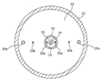
도 2a 및 2b는 본 실시예에 있어서의 서셉터 상부의 구조를 나타내는 도면으로서, 도 2a는 단면도, 도 2b는 도 2a의 A-A 화살표 단면의 평면도이다. 서셉터(2)의 상부에는 유전체층(34)이 형성되고, 그 바로 아래에는 도전 막으로 이루어지는 내부 전극(17)이 매립되어 있다. 내부 전극(17)에는 급전선(13)에 의해 직류 고전 압이 인가된다. 급전선(13)의 주위에는 원통형상의 절연 부재(14)가 배치되어 누전을 방지한다. 서셉터(2)는 열전도율이 높은 재료 예를 들면 금속으로 구성되고, 그 내부에 냉매유로(18)가 마련되어 있다. 냉매유로(18)에는 배관(20a)으로부터 냉매가 공급되고, 배관(20b)으로부터 배출되어, 냉매가 순환한다. 2A and 2B are views showing the structure of the susceptor upper part in this embodiment, FIG. 2A is a sectional view, and FIG. 2B is a plan view of an A-A arrow cross section in FIG. 2A. A
서셉터(2)의 상단 바깥가장자리 전체 둘레에는 둘레가장자리 환상 볼록부(21)가 마련되고, 기판(W)은 이 둘레가장자리 환상 볼록부(21)의 위에 탑재된다. 이 때문에, 기판(W)과 유전체층(34)의 사이에는 약간의 공간이 형성된다. 또한, 절연 부재(14)를 둘러싸도록, 내부 환상 볼록부(31)가 마련되어 있고, 상기의 공간은 내측 영역(32)과 외측 영역(33)으로 구획되어 있다. The peripheral edge annular
내측 영역(32)에는 가스 공급관(23a)을 거쳐서 냉각 가스가 공급되고, 가스 배출관(35a)으로부터 배출된다. 외측 영역(33)에는 가스 공급관(23b)을 거쳐서 냉각 가스가 공급되고, 가스 배출관(35b)으로부터 배출된다. 가스 공급관(23a, 23b) 및 가스 배출관(35a, 35b)에는 유량 조절 밸브(36)가 배치되고, 또한 가스 공급관(23a, 23b)에는 각각 압력계(37)가 설치되어 있다. 유량 조절 밸브(36)를 조절하는 것에 의해, 내측 영역(32) 및 외측 영역(33)의 압력을 원하는 값으로 제어할 수 있다. Cooling gas is supplied to the
또, 본 실시예에 있어서는 냉각 가스의 공급관과 배출관이 마련되어 있지만, 배출관은 반드시 필요하지는 않다. 둘레가장자리 환상 볼록부(21)나 내부 환상 볼록부(31)와 기판(W)의 사이의 시일의 방법(밀착성의 정도)을 조정하는 것에 의해, 냉각 가스를 챔버내에 누출시킴으로써 가스류를 발생시킬 수 있기 때문이다.In addition, in this embodiment, although the supply pipe and the discharge pipe of a cooling gas are provided, the discharge pipe is not necessarily required. By adjusting the sealing method (degree of adhesion) between the circumferential annular
본 발명에 있어서, 서셉터(2)와 기판(W)의 간극을 내측 영역(32)과 외측 영역(33)으로 구획하고, 각각 독립적으로 냉각 가스를 흘리는 이유는 기판(W)로부터의 발열량을 조절하여, 기판 전체에서 그 온도를 균일하게 유지하기 위해서이다. 급전선(13)의 주위의 절연 부재(14)는 열전도도가 작기 때문에 냉매에 전열하기 어렵다. 그 때문에, 내측 영역(32)에서는 외측 영역(33)보다도 서셉터(2)의 표면온도가 높아지고, 기판(W)로부터 서셉터(2)에의 발열량이 낮아진다. 그래서, 서셉터(2) 표면과 기판(W)의 간극에 흘리는 냉각 가스의 압력을, 내측 영역(32)과 외측 영역(33)에서 따로따로 제어하여, 내측 영역(32)에서의 냉각 가스를 거친 전열을 촉진시키는 것이 본 발명의 포인트이다. In the present invention, the gap between the
즉, 플라즈마 처리 장치내에 있어서는 공간의 유지 압력에 대해 공간의 대표길이가 짧기 때문에, 장치내에 도입된 냉각 가스는 분자류 영역에 있다. 분자류 영역에서는 가스의 열전도도가 그 압력에 비례하므로, 내측 영역(32)의 압력을 외측 영역(33)보다도 높게 하는 것에 의해, 기판(W)로부터 서셉터(2)에 전열을 촉진할 수 있고, 이것에 의해 기판(W)의 전체의 온도를 균일하게 할 수 있다. 이것이 가능하게 되는 근거에 대해서는 후에 상세하게 설명한다. That is, in the plasma processing apparatus, since the representative length of the space is short with respect to the holding pressure of the space, the cooling gas introduced into the apparatus is in the molecular flow region. In the molecular flow region, since the thermal conductivity of the gas is proportional to the pressure, the heat transfer from the substrate W to the
도 3a 및 3b은 본 발명의 제2 실시예에 있어서의 서셉터 상부의 구조를 나타내는 도면(중앙부근만 확대해서 나타냄)으로서, 도 3a는 단면도, 도 3b는 평면도이다. 이 예에 있어서는 급전선(13)의 주위의 절연 부재(14)의 주변에 이중의 내부 환상 볼록부, 즉 내측의 제 1 환상 볼록부(31a)와 외측의 제 2 환상 볼록부(31b)가 마련되어 있다. 이것에 의해, 서셉터(2)와 기판(W)의 간극은 제 1 내측 영 역(32a), 제 2 내측 영역(32b)과 외측 영역(33)으로 3분할되어 있다. 각 영역에는 각각 독립적으로 냉각 가스가 취입되고, 독립적으로 영역 내부의 압력을 제어할 수 있도록 되어 있다. 3A and 3B are diagrams showing the structure of the upper part of the susceptor in the second embodiment of the present invention (only the center portion is enlarged), and FIG. 3A is a sectional view and FIG. In this example, a double inner annular projection, that is, an inner first
즉, 제 1 내측 영역(32a)에는 가스 공급관(23a)을 거쳐서 냉각 가스가 공급되고, 가스 배출관(35a)으로부터 배출된다. 제 2 내측 영역(32b)에는 가스 공급관(23c)을 거쳐서 냉각 가스가 공급되고, 가스 배출관(35c)으로부터 배출된다. 또한, 외측 영역(33)에는 가스 공급관(23b)을 거쳐서 냉각 가스가 공급되고, 가스 배출관(35b)으로부터 배출된다. 가스 공급관(23a, 23b, 23c) 및 가스 배출관(35a, 35b, 35c)에는 각각 유량 조절 밸브(도시하지 않음)가 배치되어, 각 영역의 압력을 독립적으로 제어할 수 있다. 이와 같이 3개의 영역으로 분할하는 이유는 기판 온도의 제어 정밀도를 높이기 위함이지만, 상세한 것은 후술한다. That is, cooling gas is supplied to the 1st inner side area |
또, 본 실시예에서는 제 1 환상 볼록부(31a)와 제 2 환상 볼록부(31b)는 급전선(13)의 중심을 중심축으로 해서 동심원 형상으로 형성되어 있지만, 동심원의 중심이 급전선(13)의 중심과 일치하고 있지 않아도, 대략 그 부근에 있으면 좋다. In the present embodiment, the first
도 4a 및 4b는 본 발명의 제 3 실시예에 있어서의 서셉터 상부의 구조를 나타내는 도면으로서, 도 4a는 단면도, 도 4b는 도 4a의 B-B 화살표 단면의 평면도이다. 이 예에 있어서는 급전선(13)은 서셉터(2)의 중앙이 아니라, 둘레 가장자리 부근에 한쌍, 대략 대상의 위치에 마련되어 있다. 급전선(13)의 주위가 절연 부재(14)에 의해 절연되는 것은 도 2a 및 2b와 마찬가지이다. 따라서, 각각의 절연 부재(14)의 주위에 내부 환상 볼록부(31)가 마련되고, 서셉터(2)와 기판(W)의 간극 은 2개의 내측 영역(32)과 외측 영역(33)으로 분할되어 있다. 이와 같은 구조로 하는 것에 의해서, 내부 전극(17)에의 급전선(13)이 서셉터(2)의 둘레 가장자리에 있는 경우에도, 본 발명의 목적을 달성할 수 있다. 4A and 4B are views showing the structure of the upper part of the susceptor in the third embodiment of the present invention. FIG. 4A is a sectional view, and FIG. 4B is a plan view of the cross-section B-B in FIG. 4A. In this example, the
다음에 본 발명의 근거로 되는 열해석의 결과에 대해 설명한다. 도 5는 서셉터 상부의 전열 해석의 조건 및 결과의 설명도이다. 계산을 간단히 하기 위해, 높이 방향으로만 열이 흐르는 것을 상정한 일차원의 열전도 모델에서 고려한다. 열류속(熱流束)은 어느 위치에서도 2 W/㎠의 일정값으로 하고, 냉매온도 즉 냉매유로의 표면온도는 T1(일정값), 전열층의 두께는 15 ㎜로 한다. 또한, 급전선 주위의 절연재료(AL2O3)의 열전도율은 16 W/m?K로 하고, 그 이외의 구조재료(Al)의 열전도율은 160 W/m?K로 한다. Next, the result of the thermal analysis on which the present invention is based will be described. It is explanatory drawing of the conditions and result of the electrothermal analysis of the upper part of a susceptor. In order to simplify the calculation, it is considered in the one-dimensional heat conduction model that assumes heat flows only in the height direction. The heat flux is at a constant value of 2 W /
이 조건에서 서셉터 표면의 온도를 계산한 결과, 절연재와 구조재의 표면온도의 차 △T = T2(절연재) - T2(구조재)는 16.9 ℃로 되는 것이 명백하게 되었다. 서셉터 표면 온도에 이만큼의 차가 생기면, 기판도 이것에 가까운 온도차가 생겨, 플라즈마 처리의 품질의 균일성에 악영향을 미칠 가능성이 크다. As a result of calculating the temperature of the susceptor surface under these conditions, it became clear that the difference ΔT = T 2 (insulating material)-T 2 (structural material) between the surface temperatures of the insulating material and the structural material became 16.9 ° C. If such a difference occurs in the susceptor surface temperature, the substrate also has a temperature difference close to this, which is likely to adversely affect the uniformity of the quality of the plasma treatment.
실제의 열류는 일차원이 아니라, 횡방향으로도 열이 확산하므로, 축 대상의 이차원 전열 모델에서 고려할 필요가 있다. 도 6a 및 6b는 실제의 서셉터 표면 온도 분포의 개념도와, 이것에 대응한 존 분할의 사고방식의 설명도이다. 도 6a에 나타내는 바와 같이, 표면온도 T2가 피크 형상으로 높게 되어 있는 존 1과, T2가 완만하게 경사지고 점차 감소하는 존 2와, T2가 일정값으로 되는 존 3으로 나누어진다. 따라서, 도 6b에 나타내는 바와 같이, 기판(W)와 서셉터(2)의 사이의 공간을, 제 1 환상 볼록부(31a)와 제 2 환상 볼록부(31b)로 이중으로 칸막이를 마련하여, 제 1 내측 영역(존 1)과 제 2 내측 영역(존 2)과 외측 영역(존 3)으로 분할하고, 그 압력 P가 (존 1) > (존 2) > (존 3)으로 되도록 제어하면 좋다. The actual heat flow is not only one-dimensional, but heat also diffuses in the lateral direction, so it must be considered in the two-dimensional heat transfer model of the axis target. 6A and 6B are conceptual diagrams of actual susceptor surface temperature distributions, and explanatory diagrams of a zone division thinking method corresponding thereto. As shown in Fig. 6a, the surface temperature T 2 that is to a zone which is high in the peak shape and one, T 2 is the
이와 같이 해서, 존 1~3의 압력을 적절하게 제어하는 것에 의해, 기판(W)의 온도의 균일성을 더욱 높일 수 있다. 전술한 제 2 실시예는 이러한 사고방식에 의거하여, 제 1 실시예보다도 정밀한 기판 온도의 제어를 실행하는 것을 의도한 것이다. 또, 존의 분할수를 더욱 많게 해도 좋다. In this way, the temperature uniformity of the substrate W can be further increased by appropriately controlling the pressure in the
또한, 제 3 실시예와 같은 급전선(13)이 서셉터(2)의 둘레 가장자리부에 마련되어 있는 경우에도, 각 급전선(13)의 절연부(14)에 이중 또는 그 이상의 환상 볼록부(31)를 마련하여, 각 3존 이상으로 분할해도 좋다. 이것에 의해, 기판 온도 제어의 정밀도를 높일 수 있다. Further, even when the
다음에, 냉각 가스 압력의 전열에 미치는 영향에 대해 설명한다. 플라즈마 처리 등의 진공 처리 장치에 있어서는 기판(W)과 서셉터(2)의 사이의 공간에 도입된 냉각 가스는 분자류 영역에 있고, 그 열전도도는 절대압력에 비례한다. 그 때문에, 냉각 가스를 거쳐서 기판(W)으로부터 서셉터(2)에 전도되는 열량은 냉각 가스의 압력에 비례적으로 증대한다. 그래서, 열류속과 서셉터 표면 온도가 일정으로 해서, 냉각 가스(He)의 압력과 기판온도의 관계를 시산(試算)한 결과의 예를 도 7 에 나타낸다. 동일 도면에 있어서는 He 압력 50 Torr의 경우를 기준으로 하고, 이 때에 기판온도가 0 ℃가 되도록 조건을 설정하여, He 압력이 변경되었을 때의 기판온도를 계산하였다.Next, the influence on the heat transfer of the cooling gas pressure is demonstrated. In a vacuum processing apparatus such as plasma processing, the cooling gas introduced into the space between the substrate W and the
도 7에 보이는 바와 같이, 기판온도는 He 압력 50 Torr의 경우를 0 ℃로 해서, He 압력의 저하와 함께 상승하고, 압력 20 Torr에서 약 10 ℃, 10 Torr에서 약 20 ℃로 된다. 앞의 도 5에서 나타낸 절연재와 구조재의 표면온도의 차 16.9 ℃에 상당하는 바와 같이, 기판(W)으로부터 서셉터(2)에의 전열량을 증가시키기 위해서는 절연재의 부분(내측 영역(32))의 He 압력을 50 Torr로 하고, 구조재의 부분(외측 영역(33))의 압력을 13.5 Torr 정도로 하면 좋은 것이 이해된다. 이상은 대략의 추정이지만, 본 발명의 방법에서 He 압력을 상기와 같이 제어하는 것에 곤란은 없고, 본 발명에 의해 급전선 부분의 기판온도의 특이성을 회피할 수 있는 것이 명백하게 되었다. As shown in Fig. 7, the substrate temperature rises with a decrease in the He pressure, with a He pressure of 50 Torr of 0 deg. C, and a temperature of about 10 deg. C at 20 Torr and about 20 deg. As the difference between the surface temperature of the insulating material and the structural material shown in FIG. 5 is 16.9 ° C, in order to increase the heat transfer amount from the substrate W to the
도 1은 발명의 실시에 이용되는 플라즈마 처리 장치(플라즈마 에칭 장치)의 전체의 개략 구성을 나타내는 도면. BRIEF DESCRIPTION OF THE DRAWINGS The figure which shows schematic structure of the whole plasma processing apparatus (plasma etching apparatus) used for implementation of this invention.
도 2a 및 2b는 본 발명의 일실시예에 있어서의 서셉터 상부의 구조를 나타내는 도면. 2A and 2B are views showing the structure of the susceptor upper part in one embodiment of the present invention.
도 3a 및 3b는 본 발명의 제 2 실시예에 있어서의 서셉터 상부의 구조를 나타내는 도면. 3A and 3B show a structure of an upper susceptor in a second embodiment of the present invention.
도 4a 및 4b는 본 발명의 제 3 실시예에 있어서의 서셉터 상부의 구조를 나타내는 도면. 4A and 4B are views showing the structure of the upper part of the susceptor in the third embodiment of the present invention.
도 5는 서셉터 상부의 전열 해석의 조건 및 결과의 설명도. 5 is an explanatory diagram of conditions and results of an electrothermal analysis on an upper part of the susceptor.
도 6a 및 6b은 실제의 서셉터 표면 온도 분포와, 이것에 대응한 존 분할의 사고방식을 나타내는 설명도. 6A and 6B are explanatory diagrams showing an actual susceptor surface temperature distribution and a thinking scheme of zone division corresponding thereto.
도 7은 냉각 가스의 압력과 기판온도의 관계를 시산한 결과의 예를 나타내는 도면. Fig. 7 is a diagram showing an example of the result of calculating the relationship between the pressure of the cooling gas and the substrate temperature.
도면의 주요부분에 관한 부호의 설명Explanation of symbols about main parts of the drawings
1: 챔버 2: 서셉터(탑재대)1: chamber 2: susceptor (mounting stage)
3: 통형상 유지부 4: 통형상 지지부3: cylindrical holder 4: cylindrical holder
5: 포커스 링 6: 배기로5: focus ring 6: exhaust passage
7: 배플판 8: 배기관7: baffle plate 8: exhaust pipe
9: 배기장치 10: 반입출구9: exhaust system 10: inlet and outlet
11: 게이트 밸브 12: 직류 고압 전원11: gate valve 12: DC high voltage power supply
13: 급전선 14: 절연 부재13: feeder 14: insulation member
15: 샤워헤드 16: 정전 척15: showerhead 16: electrostatic chuck
17: 내부 전극 18: 냉매 유로17: internal electrode 18: refrigerant path
19: 냉매 유닛 20, 20a, 20b: 배관19:
21: 둘레가장자리 환상 볼록부 22: 냉각 가스 공급부21: circumferential edge annular convex portion 22: cooling gas supply portion
23a, 23b, 23c: 가스 공급관 24: 전극판23a, 23b, 23c: gas supply pipe 24: electrode plate
25: 전극 지지체 26: 버퍼실25
27: 가스 도입구 28: 처리 가스 공급부27: gas inlet 28: process gas supply part
29: 가스 도입관 30: 링 자석29: gas introduction pipe 30: ring magnet
31, 31a, 31b: 내부 환상 볼록부 32, 32a, 32b: 내측 영역31, 31a, 31b: inner annular
33: 외측 영역 34: 유전체층33: outer region 34: dielectric layer
35a, 35b, 35c: 가스 배출관 36: 유량 조절 밸브35a, 35b, 35c: gas discharge line 36: flow control valve
37: 압력계 W: 기판(반도체 웨이퍼) 37: pressure gauge W: substrate (semiconductor wafer)
Claims (13)
Applications Claiming Priority (2)
| Application Number | Priority Date | Filing Date | Title |
|---|---|---|---|
| JPJP-P-2008-026235 | 2008-02-06 | ||
| JP2008026235A JP5222442B2 (en) | 2008-02-06 | 2008-02-06 | Substrate mounting table, substrate processing apparatus, and temperature control method for substrate to be processed |
Publications (2)
| Publication Number | Publication Date |
|---|---|
| KR20090086171A KR20090086171A (en) | 2009-08-11 |
| KR101115659B1 true KR101115659B1 (en) | 2012-03-14 |
Family
ID=40404297
Family Applications (1)
| Application Number | Title | Priority Date | Filing Date |
|---|---|---|---|
| KR1020090009726A KR101115659B1 (en) | 2008-02-06 | 2009-02-06 | Substrate mounting table, substrate processing apparatus and substrate temperature control method |
Country Status (6)
| Country | Link |
|---|---|
| US (1) | US8696862B2 (en) |
| EP (1) | EP2088616A3 (en) |
| JP (1) | JP5222442B2 (en) |
| KR (1) | KR101115659B1 (en) |
| CN (1) | CN101504928B (en) |
| TW (1) | TWI445124B (en) |
Families Citing this family (40)
| Publication number | Priority date | Publication date | Assignee | Title |
|---|---|---|---|---|
| JP5418300B2 (en) * | 2010-02-26 | 2014-02-19 | 株式会社Ihi | In-furnace transport roll |
| CN101866826B (en) * | 2010-04-29 | 2012-04-11 | 中微半导体设备(上海)有限公司 | Fluid conveying device for vacuum processing system |
| JP5101665B2 (en) * | 2010-06-30 | 2012-12-19 | 東京エレクトロン株式会社 | Substrate mounting table, substrate processing apparatus, and substrate processing system |
| TWI762170B (en) * | 2011-10-05 | 2022-04-21 | 美商應用材料股份有限公司 | Plasma processing apparatus comprising symmetric plasma process chamber and lid assembly for the same |
| JP5993568B2 (en) * | 2011-11-09 | 2016-09-14 | 東京エレクトロン株式会社 | Substrate mounting system, substrate processing apparatus, electrostatic chuck, and substrate cooling method |
| DE102012101923B4 (en) * | 2012-03-07 | 2019-11-07 | Osram Opto Semiconductors Gmbh | Substrate carrier assembly, coating system with substrate carrier assembly and method for performing a coating method |
| JP5946365B2 (en) * | 2012-08-22 | 2016-07-06 | 株式会社アルバック | Electrostatic adsorption device, residual adsorption removal method |
| JP6010433B2 (en) * | 2012-11-15 | 2016-10-19 | 東京エレクトロン株式会社 | Substrate mounting table and substrate processing apparatus |
| EP3594998B1 (en) * | 2013-03-06 | 2022-01-05 | Plasma-Therm, Llc | Method for plasma dicing a semi-conductor wafer |
| US20150060013A1 (en) * | 2013-09-05 | 2015-03-05 | Applied Materials, Inc. | Tunable temperature controlled electrostatic chuck assembly |
| CN104465450B (en) * | 2013-09-22 | 2017-05-10 | 中微半导体设备(上海)有限公司 | Gas supply device and method for cooling static sucker |
| CN104752301B (en) * | 2013-12-31 | 2018-05-25 | 北京北方华创微电子装备有限公司 | A kind of electrostatic chuck and chamber |
| CN103792974B (en) * | 2014-01-22 | 2015-12-02 | 清华大学 | A kind of can the heating plate of quick meticulous adjustment temperature field space distribution and control method |
| WO2015145663A1 (en) * | 2014-03-27 | 2015-10-01 | 株式会社日立国際電気 | Semiconductor device manufacturing method and substrate processing apparatus |
| CN103972013B (en) | 2014-05-14 | 2016-08-24 | 京东方科技集团股份有限公司 | A kind of vacuum equipment |
| JP6469985B2 (en) * | 2014-07-28 | 2019-02-13 | 株式会社日立ハイテクノロジーズ | Plasma processing equipment |
| US9613839B2 (en) * | 2014-11-19 | 2017-04-04 | Varian Semiconductor Equipment Associates, Inc. | Control of workpiece temperature via backside gas flow |
| KR101670457B1 (en) * | 2014-11-28 | 2016-10-31 | 세메스 주식회사 | Support unit and apparatus for treating substrate with the support unit |
| JP2016136554A (en) * | 2015-01-23 | 2016-07-28 | 株式会社日立ハイテクノロジーズ | Plasma processing apparatus |
| US10515786B2 (en) * | 2015-09-25 | 2019-12-24 | Tokyo Electron Limited | Mounting table and plasma processing apparatus |
| WO2017126534A1 (en) * | 2016-01-19 | 2017-07-27 | 住友大阪セメント株式会社 | Electrostatic chuck device |
| JP6847610B2 (en) * | 2016-09-14 | 2021-03-24 | 株式会社Screenホールディングス | Heat treatment equipment |
| DE102017200588A1 (en) * | 2017-01-16 | 2018-07-19 | Ers Electronic Gmbh | Device for tempering a substrate and corresponding manufacturing method |
| WO2018183557A1 (en) * | 2017-03-31 | 2018-10-04 | Lam Research Corporation | Electrostatic chuck with flexible wafer temperature control |
| JP7030557B2 (en) * | 2018-02-27 | 2022-03-07 | 日本特殊陶業株式会社 | Holding device |
| JP7145625B2 (en) * | 2018-03-07 | 2022-10-03 | 東京エレクトロン株式会社 | Substrate mounting structure and plasma processing apparatus |
| CN110767568B (en) * | 2018-07-26 | 2022-05-27 | 北京北方华创微电子装备有限公司 | Pressure regulating assembly, lower electrode device, process chamber and semiconductor processing equipment |
| JP2020043171A (en) * | 2018-09-07 | 2020-03-19 | 東京エレクトロン株式会社 | Temperature control method |
| JP7209515B2 (en) * | 2018-11-27 | 2023-01-20 | 東京エレクトロン株式会社 | Substrate holding mechanism and deposition equipment |
| CN111326390B (en) * | 2018-12-17 | 2023-09-12 | 中微半导体设备(上海)股份有限公司 | Radio frequency electrode assembly and plasma processing apparatus |
| US11875970B2 (en) * | 2018-12-17 | 2024-01-16 | Advanced Micro-Fabrication Equipment Inc. China | Radio frequency electrode assembly for plasma processing apparatus, and plasma processing apparatus |
| JP7186096B2 (en) * | 2019-01-09 | 2022-12-08 | 東京エレクトロン株式会社 | Hot plate cooling method and heat treatment apparatus |
| JP7254542B2 (en) * | 2019-02-01 | 2023-04-10 | 東京エレクトロン株式会社 | Mounting table and substrate processing device |
| JP7407529B2 (en) | 2019-07-10 | 2024-01-04 | 東京エレクトロン株式会社 | Substrate mounting table, substrate processing equipment, and temperature control method |
| WO2021060843A1 (en) * | 2019-09-27 | 2021-04-01 | 주식회사 뷰웍스 | Substrate fixation device for scintillator deposition, substrate deposition device comprising same, and deposition method of scintillator by using same |
| JP7402037B2 (en) | 2019-12-23 | 2023-12-20 | 日本特殊陶業株式会社 | electrostatic chuck |
| CN113053715B (en) * | 2019-12-27 | 2023-03-31 | 中微半导体设备(上海)股份有限公司 | Lower electrode assembly, plasma processing device and working method thereof |
| CN113130279B (en) * | 2019-12-30 | 2023-09-29 | 中微半导体设备(上海)股份有限公司 | Lower electrode assembly, plasma processing device and working method thereof |
| JP7442347B2 (en) * | 2020-03-06 | 2024-03-04 | 東京エレクトロン株式会社 | Substrate processing equipment and substrate processing method |
| CN115552586A (en) * | 2020-05-25 | 2022-12-30 | 日本碍子株式会社 | Electrostatic chuck |
Citations (4)
| Publication number | Priority date | Publication date | Assignee | Title |
|---|---|---|---|---|
| JP2003282692A (en) * | 2002-03-27 | 2003-10-03 | Matsushita Electric Ind Co Ltd | Substrate carrying tray and substrate processing apparatus using this tray |
| JP2004172202A (en) * | 2002-11-18 | 2004-06-17 | Anelva Corp | Electrostatic chuck device |
| JP2005079415A (en) * | 2003-09-02 | 2005-03-24 | Hitachi High-Technologies Corp | Plasma processing apparatus |
| KR20060001172A (en) * | 2004-06-30 | 2006-01-06 | 주성엔지니어링(주) | Electrode static chuck |
Family Cites Families (16)
| Publication number | Priority date | Publication date | Assignee | Title |
|---|---|---|---|---|
| JP3086970B2 (en) * | 1991-07-03 | 2000-09-11 | 東京エレクトロン株式会社 | Substrate processing equipment |
| JPH0567551A (en) | 1991-09-05 | 1993-03-19 | Canon Inc | Wafer chuck |
| US5738165A (en) * | 1993-05-07 | 1998-04-14 | Nikon Corporation | Substrate holding apparatus |
| TW277139B (en) * | 1993-09-16 | 1996-06-01 | Hitachi Seisakusyo Kk | |
| US5609720A (en) * | 1995-09-29 | 1997-03-11 | Lam Research Corporation | Thermal control of semiconductor wafer during reactive ion etching |
| JPH09213777A (en) * | 1996-01-31 | 1997-08-15 | Kyocera Corp | Electrostatic chuck |
| JP2000317761A (en) | 1999-03-01 | 2000-11-21 | Toto Ltd | Electrostatic chuck and attracting method |
| US6740853B1 (en) * | 1999-09-29 | 2004-05-25 | Tokyo Electron Limited | Multi-zone resistance heater |
| JP4317329B2 (en) | 2000-01-20 | 2009-08-19 | 日本碍子株式会社 | Electrostatic chuck |
| US20050211385A1 (en) * | 2001-04-30 | 2005-09-29 | Lam Research Corporation, A Delaware Corporation | Method and apparatus for controlling spatial temperature distribution |
| US7161121B1 (en) * | 2001-04-30 | 2007-01-09 | Lam Research Corporation | Electrostatic chuck having radial temperature control capability |
| JP3810300B2 (en) * | 2001-10-30 | 2006-08-16 | 京セラ株式会社 | Electrostatic chuck |
| US7156951B1 (en) * | 2002-06-21 | 2007-01-02 | Lam Research Corporation | Multiple zone gas distribution apparatus for thermal control of semiconductor wafer |
| JP4540407B2 (en) * | 2004-06-28 | 2010-09-08 | 京セラ株式会社 | Electrostatic chuck |
| US8021521B2 (en) * | 2005-10-20 | 2011-09-20 | Applied Materials, Inc. | Method for agile workpiece temperature control in a plasma reactor using a thermal model |
| US8226769B2 (en) * | 2006-04-27 | 2012-07-24 | Applied Materials, Inc. | Substrate support with electrostatic chuck having dual temperature zones |
-
2008
- 2008-02-06 JP JP2008026235A patent/JP5222442B2/en not_active Expired - Fee Related
-
2009
- 2009-02-05 EP EP09152132A patent/EP2088616A3/en not_active Withdrawn
- 2009-02-05 US US12/366,177 patent/US8696862B2/en active Active
- 2009-02-05 TW TW098103675A patent/TWI445124B/en not_active IP Right Cessation
- 2009-02-06 KR KR1020090009726A patent/KR101115659B1/en active IP Right Grant
- 2009-02-06 CN CN2009100051604A patent/CN101504928B/en not_active Expired - Fee Related
Patent Citations (4)
| Publication number | Priority date | Publication date | Assignee | Title |
|---|---|---|---|---|
| JP2003282692A (en) * | 2002-03-27 | 2003-10-03 | Matsushita Electric Ind Co Ltd | Substrate carrying tray and substrate processing apparatus using this tray |
| JP2004172202A (en) * | 2002-11-18 | 2004-06-17 | Anelva Corp | Electrostatic chuck device |
| JP2005079415A (en) * | 2003-09-02 | 2005-03-24 | Hitachi High-Technologies Corp | Plasma processing apparatus |
| KR20060001172A (en) * | 2004-06-30 | 2006-01-06 | 주성엔지니어링(주) | Electrode static chuck |
Also Published As
| Publication number | Publication date |
|---|---|
| JP2009188162A (en) | 2009-08-20 |
| EP2088616A2 (en) | 2009-08-12 |
| CN101504928B (en) | 2011-08-03 |
| EP2088616A3 (en) | 2013-01-02 |
| TW201001612A (en) | 2010-01-01 |
| JP5222442B2 (en) | 2013-06-26 |
| US20090194264A1 (en) | 2009-08-06 |
| CN101504928A (en) | 2009-08-12 |
| TWI445124B (en) | 2014-07-11 |
| US8696862B2 (en) | 2014-04-15 |
| KR20090086171A (en) | 2009-08-11 |
Similar Documents
| Publication | Publication Date | Title |
|---|---|---|
| KR101115659B1 (en) | Substrate mounting table, substrate processing apparatus and substrate temperature control method | |
| US11004716B2 (en) | Electrostatic chuck assembly and semiconductor manufacturing apparatus including the same | |
| JP6453240B2 (en) | Shower head with removable gas distribution plate | |
| KR100270207B1 (en) | Plasma treatment apparatus | |
| KR100748372B1 (en) | A method and apparatus for thermal control of a semiconductor substrate | |
| US20080053958A1 (en) | Plasma processing apparatus | |
| US20080260966A1 (en) | Plasma processing method | |
| US11152196B2 (en) | Substrate processing apparatus | |
| US20230326724A1 (en) | Plasma processing apparatus | |
| US11955314B2 (en) | Plasma processing apparatus | |
| JP2006351887A (en) | Plasma processing device | |
| US11342165B2 (en) | Plasma processing method | |
| US11862436B2 (en) | Plasma processing apparatus and plasma processing method | |
| US10847348B2 (en) | Plasma processing apparatus and plasma processing method | |
| CN110581051B (en) | Apparatus and method for processing substrate | |
| KR20210089787A (en) | Electrostatic chuck with improved thermal coupling for temperature sensitive processes | |
| KR100999588B1 (en) | Apparatus and method for processing substrate | |
| JP7090149B2 (en) | Plasma processing equipment and plasma etching method | |
| KR20160145865A (en) | Electrostatic chuck and substrate treating apparatus | |
| JP2006060073A (en) | Plasma processing equipment | |
| JP2005203426A (en) | Electrode for mounting wafer | |
| US20210020408A1 (en) | Substrate support assembly, substrate processing apparatus, and edge ring | |
| KR20110083979A (en) | Plasma processing apparatus | |
| CN115938896A (en) | Support unit and apparatus for processing substrate | |
| TW202309312A (en) | Plasma processing apparatus |
Legal Events
| Date | Code | Title | Description |
|---|---|---|---|
| A201 | Request for examination | ||
| E902 | Notification of reason for refusal | ||
| E701 | Decision to grant or registration of patent right | ||
| GRNT | Written decision to grant | ||
| FPAY | Annual fee payment |
Payment date: 20150105 Year of fee payment: 4 |
|
| FPAY | Annual fee payment |
Payment date: 20160105 Year of fee payment: 5 |
|
| FPAY | Annual fee payment |
Payment date: 20170103 Year of fee payment: 6 |
|
| FPAY | Annual fee payment |
Payment date: 20180119 Year of fee payment: 7 |
|
| FPAY | Annual fee payment |
Payment date: 20190117 Year of fee payment: 8 |