KR101035184B1 - Semiconductor test apparatus - Google Patents
Semiconductor test apparatus Download PDFInfo
- Publication number
- KR101035184B1 KR101035184B1 KR1020047020030A KR20047020030A KR101035184B1 KR 101035184 B1 KR101035184 B1 KR 101035184B1 KR 1020047020030 A KR1020047020030 A KR 1020047020030A KR 20047020030 A KR20047020030 A KR 20047020030A KR 101035184 B1 KR101035184 B1 KR 101035184B1
- Authority
- KR
- South Korea
- Prior art keywords
- signal
- data
- information
- cross point
- timing
- Prior art date
Links
- 238000012360 testing method Methods 0.000 title claims abstract description 61
- 239000004065 semiconductor Substances 0.000 title claims abstract description 50
- 230000007704 transition Effects 0.000 claims abstract description 86
- 238000005259 measurement Methods 0.000 claims abstract description 47
- 238000004364 calculation method Methods 0.000 claims abstract description 12
- 238000005070 sampling Methods 0.000 claims description 22
- 230000000630 rising effect Effects 0.000 claims description 15
- 238000006243 chemical reaction Methods 0.000 claims description 13
- 238000012545 processing Methods 0.000 claims description 10
- 238000013500 data storage Methods 0.000 claims description 7
- 238000000034 method Methods 0.000 claims 5
- 238000003708 edge detection Methods 0.000 description 11
- 230000006870 function Effects 0.000 description 5
- 238000010998 test method Methods 0.000 description 5
- 239000000470 constituent Substances 0.000 description 4
- 238000010586 diagram Methods 0.000 description 4
- 230000000694 effects Effects 0.000 description 3
- 230000001360 synchronised effect Effects 0.000 description 3
- 238000012546 transfer Methods 0.000 description 3
- 230000005540 biological transmission Effects 0.000 description 2
- 238000011156 evaluation Methods 0.000 description 1
- 230000001788 irregular Effects 0.000 description 1
- 238000004519 manufacturing process Methods 0.000 description 1
Images
Classifications
-
- G—PHYSICS
- G01—MEASURING; TESTING
- G01R—MEASURING ELECTRIC VARIABLES; MEASURING MAGNETIC VARIABLES
- G01R31/00—Arrangements for testing electric properties; Arrangements for locating electric faults; Arrangements for electrical testing characterised by what is being tested not provided for elsewhere
- G01R31/28—Testing of electronic circuits, e.g. by signal tracer
- G01R31/317—Testing of digital circuits
- G01R31/3181—Functional testing
- G01R31/319—Tester hardware, i.e. output processing circuits
- G01R31/3193—Tester hardware, i.e. output processing circuits with comparison between actual response and known fault free response
- G01R31/31937—Timing aspects, e.g. measuring propagation delay
-
- G—PHYSICS
- G01—MEASURING; TESTING
- G01R—MEASURING ELECTRIC VARIABLES; MEASURING MAGNETIC VARIABLES
- G01R25/00—Arrangements for measuring phase angle between a voltage and a current or between voltages or currents
-
- G—PHYSICS
- G01—MEASURING; TESTING
- G01R—MEASURING ELECTRIC VARIABLES; MEASURING MAGNETIC VARIABLES
- G01R31/00—Arrangements for testing electric properties; Arrangements for locating electric faults; Arrangements for electrical testing characterised by what is being tested not provided for elsewhere
- G01R31/28—Testing of electronic circuits, e.g. by signal tracer
- G01R31/317—Testing of digital circuits
- G01R31/3181—Functional testing
- G01R31/319—Tester hardware, i.e. output processing circuits
- G01R31/31903—Tester hardware, i.e. output processing circuits tester configuration
- G01R31/31908—Tester set-up, e.g. configuring the tester to the device under test [DUT], down loading test patterns
- G01R31/3191—Calibration
-
- G—PHYSICS
- G01—MEASURING; TESTING
- G01R—MEASURING ELECTRIC VARIABLES; MEASURING MAGNETIC VARIABLES
- G01R31/00—Arrangements for testing electric properties; Arrangements for locating electric faults; Arrangements for electrical testing characterised by what is being tested not provided for elsewhere
- G01R31/28—Testing of electronic circuits, e.g. by signal tracer
- G01R31/317—Testing of digital circuits
- G01R31/3181—Functional testing
- G01R31/319—Tester hardware, i.e. output processing circuits
- G01R31/31917—Stimuli generation or application of test patterns to the device under test [DUT]
- G01R31/31922—Timing generation or clock distribution
Landscapes
- Physics & Mathematics (AREA)
- General Physics & Mathematics (AREA)
- Engineering & Computer Science (AREA)
- General Engineering & Computer Science (AREA)
- Tests Of Electronic Circuits (AREA)
Abstract
DUT로부터 출력되는 차동 클럭 신호 CLK의 크로스포인트와, 데이터 신호 DATA의 양 신호의 타이밍을 측정하고, 양 신호간의 상대적인 위상차를 구함으로써, 양호한 디바이스의 양부(良否) 판정을 실현 가능하게 한다. 피시험 디바이스로부터 출력되는 한쪽의 차동 출력 신호의 크로스포인트의 타이밍을 측정하여 얻은 크로스포인트 정보 Tcross를 출력하는 차동 신호 타이밍 측정 수단과, DUT로부터 출력되는 다른쪽의 비차동 출력 신호의 논리가 천이하는 천이 타이밍을 측정하여 얻은 데이터 변화점 정보 Tdata를 출력하는 비차동 신호 타이밍 측정 수단과, 양 출력 신호를 동시에 측정하여 얻은 크로스포인트 정보 Tcross와 데이터 변화점 정보 Tdata의 양자간의 상대적인 위상차를 구하여 얻은 위상차 ΔT를 출력하는 위상차 산출 수단과, 위상차 ΔT를 받아서 양부 판정을 수행하는 소정의 임계값에 기초하여 임계값 DUT의 상대적인 위상 관계의 양부를 판정하는 양부 판정 수단을 구비한다.The cross point of the differential clock signal CLK output from the DUT and the timing of the both signals of the data signal DATA are measured and the relative phase difference between the both signals is determined. Differential signal timing measurement means for outputting cross point information Tcross obtained by measuring the timing of a cross point of one differential output signal outputted from the DUT, and a comparator for comparing the logic of the other non-differential output signal output from the DUT A non-differential signal timing measurement means for outputting data change point information Tdata obtained by measuring the transition timing and a phase difference DELTA T obtained by obtaining a relative phase difference between the cross point information Tcross obtained by simultaneously measuring both output signals and the data change point information Tdata And positive and negative determination means for determining the relative phase relationship of the threshold value DUT on the basis of the predetermined threshold value for performing the positive / negative determination in response to the phase difference? T.
반도체 시험, 차동 클럭 신호, 크로스포인트, 위상차 산출, 신호 타이밍 측정Semiconductor test, differential clock signal, crosspoint, phase difference calculation, signal timing measurement
Description
본 발명은 차동 클럭 신호를 출력하는 피시험 디바이스(DUT)를 시험하는 반도체 시험 장치에 관한 것이다. 특히, DUT로부터 출력되는 하나의 차동 클럭 신호 CLK의 크로스포인트와, DUT로부터 출력되는 다른쪽의 데이터 신호 DATA에 대한 상대적인 위상차를 시험하는 반도체 시험 장치에 관한 것이다.The present invention relates to a semiconductor test apparatus for testing a device under test (DUT) that outputs a differential clock signal. In particular, the present invention relates to a semiconductor test apparatus for testing a relative phase difference between a cross point of one differential clock signal CLK output from a DUT and the other data signal DATA output from the DUT.
본원에 관련되는 배경 기술을 개시한다. 일본 특허출원 2000-178917호(반도체 디바이스 시험 방법·반도체 디바이스 시험 장치)에서는 데이터의 판독에 동기하여 데이터의 전달에 이용되는 기준 클럭 DQS를 출력하는 반도체 디바이스를 단시간에 고정밀도로 시험하는 시험 방법을 해결하고 있다.The background art relating to the present invention is disclosed. In Japanese Patent Application No. 2000-178917 (Semiconductor Device Test Method and Semiconductor Device Test Apparatus), a test method for testing a semiconductor device that outputs a reference clock DQS used for transferring data in synchronism with data reading in a short period of time is solved .
또한, 일본 특허출원 2000-9113호(반도체 디바이스 시험 방법·반도체 디바이스 시험 장치)에서는 데이터의 판독에 동기하여 데이터의 전달에 이용되는 기준 클럭 DQS를 출력하는 반도체 디바이스를 단시간에 고정밀도로 시험하는 시험 방법을 해결하고 있다.In Japanese Patent Application 2000-9113 (semiconductor device testing method and semiconductor device testing apparatus), a test method for testing a semiconductor device that outputs a reference clock DQS used for transferring data in synchronization with data reading in a short time with high accuracy .
또한, 일본 특허출원 2000-204757호(반도체 디바이스 시험 방법·반도체 디바이스 시험 장치)에서는 데이터의 판독 출력과 동기하여 기준 클럭을 출력하고, 이 기준 클럭을 데이터의 전달에 제공하는 반도체 디바이스에 있어서, 기준 클럭과 데이터간의 위상차에 따라서 불량으로 판정하는 시험 방법을 해결하고 있다.Japanese Patent Application No. 2000-204757 (Semiconductor Device Test Method and Semiconductor Device Test Apparatus) discloses a semiconductor device that outputs a reference clock in synchronization with a readout output of data and provides the reference clock to the transfer of data, And a test method for judging a failure according to a phase difference between a clock and data is solved.
그러나, 이들 배경 기술에서는 차동 클럭 신호 CLK의 크로스포인트를 특정할 수 없으므로, 다른 신호간의 상대적인 위상차를 적확하게 양부 판정할 수 없다.However, in these background arts, since the cross point of the differential clock signal CLK can not be specified, it is not possible to accurately determine the relative phase difference between the other signals.
다음에, 본 발명에 따른 문제점을 설명한다.Next, problems according to the present invention will be described.
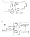
도 6의 (a)는 회로 기판상 등에서 2개의 디바이스간에서, 평형 신호로서 출력되는 차동의 클럭에 동기하여 고속의 데이터 전송을 수행하는 경우의 원리적인 회로 접속으로서, ECL이나 LVDS와 같은 차동 전송에 사용된다.6A is a schematic circuit connection in a case where high-speed data transfer is performed in synchronism with a differential clock output as a balanced signal between two devices on a circuit board or the like, and differential transmission such as ECL or LVDS .
제1 디바이스의 차동 드라이버 DR1로부터 차동 클럭 신호 CLK(정클럭 신호 CLKP, 부클럭 신호 CLKN)가 출력되고, 전송 선로를 통하여 제2 디바이스의 차동 수신기 RCV2에 공급된다. 또한, 제1 디바이스의 플립 플롭 FF1으로부터 클럭에 동기한 1개 또는 복수개의 데이터 신호 DATA가 제2 디바이스의 플립 플롭 FF2의 입력단에 공급되어, 차동 수신기 RCV2에 의한 클럭으로 리타이밍되어 사용되는 예이다. 그런데, 차동 클럭 신호는 IC의 제조 편차에 수반하는 출력 진폭의 편차나, 회로 구성에 수반하는 차동 신호간의 위상 오차 등이 있다. 또한, 차동 클럭 신호나 데이터 DATA에는 다소의 지터 성분이 포함되는 경우나 공통 모드 잡음(common-mode noise)을 발생하는 경우도 있다.The differential clock signal CLK (positive clock signal CLKP, negative clock signal CLKN) is output from the differential driver DR1 of the first device and supplied to the differential receiver RCV2 of the second device through the transmission line. One or a plurality of data signals DATA synchronized with the clock from the flip-flop FF1 of the first device are supplied to the input terminal of the flip-flop FF2 of the second device and are retimed to the clock by the differential receiver RCV2 . Incidentally, the differential clock signal has a variation in the output amplitude due to the manufacturing deviation of the IC, a phase error between the differential signals accompanying the circuit configuration, and the like. In some cases, the differential clock signal or data DATA may include some jitter components or generate common-mode noise.
이들을 고려하여, 피시험 디바이스(DUT)가 되는 제1 디바이스는 클럭과 데이터간의 출력 관계가, 규정된 위상 관계로 출력될 것이 요구되고 있다. 반도체 시험 장치에서는 차동 클럭 신호와 데이터 DATA간에 있어서, 규정된 위상 관계로 출력되고 있는지를 측정하여 양부 판정할 수 있음이 요구되고 있다. 또한, 차동 드 라이버 DR1는 출력을 오프하여 하이 임피던스 상태로 억제할 수도 있으므로, 이에 대한 시험도 가능할 필요성이 있다.Taking these into consideration, it is demanded that the first device that becomes the DUT (device under test) outputs the output relationship between clock and data in a prescribed phase relation. In the semiconductor testing apparatus, it is required that the difference between the differential clock signal and the data DATA can be judged by measuring whether or not the differential clock signal is output in a prescribed phase relationship. In addition, since the differential driver DR1 can turn off the output to suppress the high impedance state, there is a need to test the differential driver DR1.
도 6의 (b)는 DUT로부터 출력되는 차동 클럭 신호인 정클럭 신호 CLKP, 부클럭 신호 CLKN의 각각의 신호를 받기 위해, 싱글 엔드(불평형형)의 형태로 사용하는 비교기(comparator; CP)를 구비하는 구성의 반도체 시험 장치의 요부이다. 여기에서, 반도체 시험 장치는 DUT로부터 출력되는 차동 클럭 신호의 각각의 신호를 측정할 필요가 있으므로, 2채널의 싱글 엔드의 비교기 CP에서 개별적으로 수신하는 구성으로 되어 있다. 이 이유는 예를 들면, DUT의 차동 클럭 신호가 하이 임피던스 상태(Hi-Z모드)에서의 시험 항목이 있어, 이것을 시험 가능할 필요가 있기 때문이다.6B shows a comparator (CP) used in a single-ended (unbalanced) form to receive the respective signals of the positive clock signal CLKP and the sub clock signal CLKN, which are differential clock signals output from the DUT The semiconductor testing apparatus according to
도 6에 있어서, 제1 비교기 CP는 하나의 정클럭 신호 CLKP를 받아서, 소정의 임계 레벨 Vref에서 논리 신호로 변환한 후, 이를 타이밍 비교기 TC가 받아서, 원하는 타이밍의 스트로브 신호 STRB에 의해 홀드한 신호에 기초하여 양부 판정이 이루어진다.6, the first comparator CP receives one positive clock signal CLKP, converts the positive clock signal CLKP into a logic signal at a predetermined threshold level Vref, receives the positive clock signal CLKP, and outputs the logic signal to the timing comparator TC so that the signal held by the strobe signal STRB Quot ;. < / RTI >
제2 비교기 CP도 다른 쪽의 부클럭 신호 CLKN을 받아서, 소정의 임계 레벨 Vref에서 논리 신호로 변환한 후, 이를 타이밍 비교기 TC가 받아서, 원하는 타이밍의 스트로브 신호 STRB에 의해 홀드한 신호에 기초하여, 개별 입력의 싱글 엔드 신호에 대한 양부 판정이 이루어진다.The second comparator CP also receives the other sub clock signal CLKN and converts it into a logic signal at a predetermined threshold level Vref and then receives the clock signal CLKN and supplies it to the timing comparator TC to generate a logic signal based on the signal held by the strobe signal STRB at a desired timing. An affirmative decision on the single-ended signal of the individual input is made.
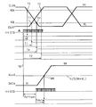
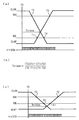
여기에서, 도 7의 (a)의 이상적인 차동 신호의 경우에는, 클럭 신호의 크로스포인트(도 7의 A점)가, 진폭의 1/2로 한 중간 전압의 임계 레벨 Vref의 전압에서 논리 신호로 변환하면 된다.Here, in the case of the ideal differential signal shown in Fig. 7A, the cross point (point A in Fig. 7) of the clock signal is shifted from the voltage of the intermediate voltage threshold level Vref by half of the amplitude to the logic signal Conversion.
그러나, 도 7의 (b)의 실제의 차동 신호예로 도시한 바와 같이, 임계 레벨 Vref에서 논리 신호로 변환하면, 목적하는 크로스포인트(도 7B 점)에 대하여, 오차가 생긴 크로스포인트(도 7의 C점)로서 검출되게 된다. 이 결과, 양 크로스포인트 사이에서 타이밍 오차(도 7의 E차)가 발생되는 난점이 있어, 타이밍 측정의 정밀도가 악화된다. 특히, 클럭 주파수가 수백MHz 이상이 되게 되면, 측정 정밀도의 영향이 커지게 된다. 반도체 시험 장치는 고정밀도의 타이밍 측정이 요구되는 측정 장치이므로, 이는 실용상의 큰 난점이다.However, as shown in the example of the actual differential signal of Fig. 7B, when the signal is converted from the threshold level Vref to the logic signal, the cross point (Fig. 7B) Point " C "). As a result, there is a difficulty in generating a timing error (E difference in Fig. 7) between both cross points, and the accuracy of the timing measurement deteriorates. Particularly, when the clock frequency becomes several hundred MHz or more, the influence of the measurement accuracy becomes large. Since the semiconductor testing apparatus is a measuring apparatus requiring a high-precision timing measurement, this is a practical difficulty.
또한, 도 7의 (c)는 차동 클럭 신호 CLK와, 데이터 신호 DATA의 양 신호의 동시 측정에 있어서, 신호간 간섭 노이즈/전원 노이즈 등의 지터 요인에 수반하여 양 신호간이 동상 변화하는 경우이다. 이 경우에는 양 신호간의 순간의 상대 위상차 Δf는 작다. 이 순간적인 위상차 Δf1를 측정하여, 정상적인 위상 범위내인지의 양부 판정을 수행할 필요가 있다.7C shows a case where both signals are changed in the same phase in accordance with a jitter factor such as inter-signal interference noise / power supply noise in the simultaneous measurement of both the differential clock signal CLK and the data signal DATA. In this case, the relative phase difference f between the two signals is small. It is necessary to measure the instantaneous phase difference DELTA f1 to determine whether or not it is within the normal phase range.
반대로, 도 7의 (d)는 차동 클럭 신호 CLK와, 데이터 신호 DATA의 양 신호의 동시 측정에 있어서, 지터 요인에 수반하여 양 신호간이 역상 변화하는 경우이다. 이 경우에는 양 신호간의 순간의 상대 위상차 Δf는 커진다. 상기의 지터 요인에 수반하는 순간적인 위상차 Δf2를 측정하여, 정상적인 위상 범위내인지의 양부 판정을 수행할 필요가 있다. 이와 같이, 양 신호간의 상대적인 위상차를 동시각에 측정하여 양부 판정할 필요성이 있다.In contrast, FIG. 7 (d) shows a case where both signals are reversed in phase with the jitter factor in the simultaneous measurement of both the differential clock signal CLK and the data signal DATA. In this case, the relative phase difference f of the instant between the two signals becomes large. It is necessary to measure the instantaneous phase difference? F2 accompanying the above-described jitter factor, and to judge whether or not it is within the normal phase range. Thus, there is a need to measure the relative phase difference between the two signals at the same time and to judge whether the two signals are correct.
앞서 설명한 바와 같이, 싱글 엔드의 비교기 CP를 2채널 적용하여, 차동 클 럭 신호 CLK의 크로스포인트의 위치를 특정하는 것은, 정클럭 신호 CLKP와 부클럭 신호 CLKN의 위상차나 진폭의 차이 등으로 크로스포인트가 이동하는 결과, 적확하게 특정할 수 없다.As described above, the two-channel single-ended comparator CP is used to specify the position of the cross point of the differential clock signal CLK. This is because the cross point of the positive clock signal CLKP and the negative clock signal CLKN As a result of the movement, it can not be precisely specified.
차동 클럭 신호 CLK와 데이터 신호 DATA의 양 신호간의 위상을 적확하게 평가하기 위해서는, 동(同) 시각에 양 신호를 샘플링 측정하고, 또한 차동 클럭 신호 CLK의 크로스포인트를 특정하고, 특정된 크로스포인트와 데이터 신호 DATA 사이의 위상을 평가하는 것이 요구된다.In order to accurately evaluate the phase between the differential clock signal CLK and the data signal DATA, both signals are sampled at the same time, the cross point of the differential clock signal CLK is specified, It is required to evaluate the phase between the data signal DATA.
그러나 종래 기술에 있어서는, 차동 클럭 신호 CLK의 크로스포인트와, 데이터 신호 DATA의 양 신호에 있어서의 상대적인 위상차를 적확하게 구하여 양부 판정할 수 없다. 반도체 시험 장치는 고정밀도의 타이밍 측정이 요구되는 측정 장치이므로, 이는 바람직하지 않아 실용상의 난점이다.However, in the prior art, the relative phase difference between the cross point of the differential clock signal CLK and both signals of the data signal DATA can not be accurately judged and can not be determined. Since the semiconductor testing apparatus is a measuring apparatus requiring timing measurement with high accuracy, this is not preferable and is a practical difficulty.
그래서, 본 발명이 해결하려는 과제는 2채널의 싱글 엔드의 비교기 CP를 적용하여, DUT로부터 출력하는 하나의 차동 클럭 신호의 크로스포인트의 타이밍을 측정하여 특정하고, DUT로부터 출력되는 다른쪽의 데이터 신호 DATA의 타이밍을 측정하고, 이로부터 양 신호간의 상대적인 위상차를 구함으로써, 양호한 디바이스의 양부 판정을 실현 가능하게 하는 반도체 시험 장치를 제공하는 것이다.Therefore, a problem to be solved by the present invention is to measure and specify the timing of a cross point of one differential clock signal output from the DUT by applying a two-channel single-ended comparator CP, The present invention provides a semiconductor testing apparatus which can measure the timing of DATA and determine the relative phase difference between the two signals from this to realize a good device judgment.
또한, 2채널의 싱글 엔드의 비교기 CP를 적용하여, DUT로부터 출력되는 차동 클럭 신호의 크로스포인트를 적확하게 측정하여 구할 수 있는 반도체 시험 장치를 제공하는 것이다.It is another object of the present invention to provide a semiconductor testing apparatus which can accurately measure the cross point of a differential clock signal output from a DUT by applying a two-channel single-ended comparator CP.
또한, DUT로부터 출력되는 차동 신호와, DUT로부터 출력되는 다른 싱글 엔드 의 신호 또는 차동 신호와의 사이에서의 상대적인 위상차를 특정할 수 있는 반도체 시험 장치를 제공하는 것이다. 또한, DUT로부터 출력되는 차동 신호와, DUT로부터 출력되는 다른 신호와의 상대적인 지터량을 측정할 수 있는 반도체 시험 장치를 제공하는 것이다.Another object of the present invention is to provide a semiconductor testing apparatus capable of specifying a relative phase difference between a differential signal output from a DUT and another differential signal outputted from a DUT or a differential signal. It is another object of the present invention to provide a semiconductor testing apparatus capable of measuring a relative jitter amount between a differential signal output from a DUT and another signal output from a DUT.
본 발명의 제1 해결 수단을 개시한다. 여기에서 도 4와 도 1은 본 발명에 따른 해결 수단을 도시하고 있다.A first solution means of the present invention is disclosed. Here, FIG. 4 and FIG. 1 show the solution means according to the invention.
상기 과제를 해결하기 위하여, 피시험 디바이스(DUT)로부터 출력되는 한쪽의 차동 출력 신호의 크로스포인트의 타이밍을 측정하여 얻은 크로스포인트 정보 Tcross를 출력하는 차동 신호 타이밍 측정 수단(예를 들면, 크로스포인트 측정부(600))를 구비하고, In order to solve the above problem, a differential signal timing measuring means (for example, a cross point measuring means) for outputting cross point information Tcross obtained by measuring a timing of a cross point of one differential output signal outputted from a DUT (600)),
DUT로부터 출력되는 다른 쪽의 비차동(싱글 엔드)의 출력 신호의 논리가 천이하는 천이 타이밍을 측정하여 얻은 데이터 변화점 정보 Tdata를 출력하는 비차동 신호 타이밍 측정 수단(예를 들면, 데이터 측정부(300))를 구비하고,Differential signal timing measuring means (for example, a data measuring unit (not shown) for outputting data change point information Tdata obtained by measuring the transition timing at which the logic of the other non-differential (single-ended) 300)
양 출력 신호를 동시에 측정하여 얻은 크로스포인트 정보 Tcross와 데이터 변화점 정보 Tdata의 양자간의 상대적인 위상차를 구하여 얻은 위상차 ΔT를 출력하는 위상차 산출 수단(예를 들면, 위상차 산출부(400))을 구비하고,(For example, a phase difference calculating section 400) for obtaining a relative phase difference between the cross point information Tcross obtained by simultaneously measuring both output signals and the data change point information Tdata,
위상차 ΔT를 받아서 양부 판정을 수행하는 소정의 상한의 임계값과 하한의 임계값 또는 한쪽 임계값에 기초하여 상기 DUT의 상대적인 위상 관계의 양부를 판정하는 양부 판정 수단(예를 들면, 양부 판정부(500))을 구비하며, 이상을 구비하 는 것을 특징으로 하는 반도체 시험 장치이다.A positive / negative determination means (for example, a positive / negative determination means (for example, a positive / negative determination means) for determining the relative phase relationship of the DUT based on a predetermined upper limit threshold value and a lower threshold value or one threshold value for receiving the phase difference? 500), and is provided with the semiconductor test apparatus.
상기 발명에 따르면, 2채널의 싱글 엔드의 비교기 CP를 적용하여, DUT로부터 출력되는 하나의 차동 신호의 크로스포인트의 타이밍을 측정하여 특정하고, DUT로부터 출력되는 다른쪽의 데이터 신호 DATA의 타이밍을 측정하여, 이로부터 양 신호간의 상대적인 위상차를 구함으로써, 양호한 디바이스의 양부 판정을 실현 가능하게 하는 반도체 시험 장치를 실현할 수 있다.According to the present invention, the timing of the cross point of one differential signal outputted from the DUT is measured and specified by applying the two-channel single-ended comparator CP, and the timing of the other data signal DATA output from the DUT is measured And by obtaining the relative phase difference between the two signals from this, it is possible to realize a semiconductor testing apparatus capable of realizing good device fairness determination.
다음에, 제2 해결 수단을 개시한다. 여기에서 도 13은 본 발명에 따른 해결 수단을 도시하고 있다.Next, a second solution means is disclosed. Here, Fig. 13 shows the solution means according to the invention.
피시험 디바이스(DUT)로부터 출력되는 한쪽의 제1 차동 출력 신호의 크로스포인트의 타이밍을 측정하여 얻은 제1 크로스포인트 정보 Tcross를 출력하는 제1 차동 신호 타이밍 측정 수단(예를 들면, 크로스포인트 측정부(600))을 구비하고,A first differential signal timing measurement means (for example, a cross point measurement section) for outputting first cross point information Tcross obtained by measuring the timing of a cross point of one of the first differential output signals outputted from the DUT, (600)),
DUT로부터 출력되는 다른쪽의 제2 차동 출력 신호의 크로스포인트의 타이밍을 측정하여 얻은 제2 크로스포인트 정보 Tcross를 출력하는 제2 차동 신호 타이밍 측정 수단(예를 들면, 크로스포인트 측정부(600))을 구비하고, (For example, the cross point measuring unit 600) for outputting the second cross point information Tcross obtained by measuring the timing of the cross point of the other second differential output signal outputted from the DUT, And,
양(兩) 차동 출력 신호를 동시에 측정하여 얻은 제1 크로스포인트 정보 Tcross와 제2 크로스포인트 정보 Tcross의 양자간의 상대적인 위상차를 구하여 얻은 위상차 ΔT를 출력하는 위상차 산출 수단(예를 들면, 위상차 산출부(400))을 구비하고,A phase difference calculating unit (for example, a phase difference calculating unit (for example, a phase difference calculating unit) for calculating a phase difference? T obtained by obtaining a relative phase difference between the first cross point information Tcross and the second cross point information Tcross obtained by simultaneously measuring both differential output signals 400)
양부 판정을 수행하는 상기 DUT에 대응한 소정의 상한 임계값과 하한 임계값 또는 한쪽 임계값에 기초하여, 상기 위상차 ΔT를 받아서 DUT의 양부를 판정하는 양부 판정 수단(예를 들면, 양부 판정부(500))을 구비하며, 이상을 구비하는 것을 특징으로 하는 반도체 시험 장치가 있다.A positive / negative determination means (for example, a positive / negative determination means (for example, a positive / negative determination means) for determining the positive and negative sides of the DUT based on a predetermined upper limit threshold value and a lower limit threshold value or one threshold value corresponding to the DUT, 500), and has a semiconductor testing apparatus as described above.
이에 따라, 2계통의 차동 신호의 상대적인 위상차를 특정하여 상대적인 위상차의 양부 판정을 수행할 수 있다.Thus, relative phase difference can be determined by specifying the relative phase difference of the two systems of differential signals.
다음에, 제3 해결 수단을 개시한다. 여기에서 도 4와 도 5와 도 1은 본 발명에 따른 해결 수단을 도시하고 있다.Next, a third solution means is disclosed. 4, Fig. 5 and Fig. 1 show the solution according to the invention.
상기 과제를 해결하기 위하여, 피시험 디바이스로부터 출력되는 한쪽의 차동 출력 신호의 크로스포인트의 타이밍을 기준으로 하여, DUT로부터 출력되는 다른쪽의 데이터 신호 DATA와의 사이의 상대적인 위상차를 양호한 정밀도로 측정하는 것이 요구되는 반도체 시험 장치에 있어서,In order to solve the above problem, it is desirable to measure the relative phase difference between the data signal DATA output from the DUT and the other data signal DATA with good precision, based on the timing of the cross point of one differential output signal output from the DUT In the required semiconductor testing apparatus,
차동 출력 신호에서의 한쪽의 신호의 천이 파형에 대하여, 크로스포인트 전후에서 2점이 측정되는 소정의 임계 레벨 VOH 및 VOL에서 논리 신호로 변환한 후, 이미 알려진 타이밍의 다상 스트로브 신호에 기초하여 샘플링 측정한 후, 코드 데이터로 변환한 2점의 타이밍 정보를 출력하는 제1 천이 정보 측정 수단(예를 들면, 제1 천이 시간 정보 수집 수단(100#1))을 구비하고, A transition waveform of one signal in the differential output signal is converted into a logic signal at a predetermined threshold level VOH and VOL at which two points are measured before and after the cross point and then sampled and measured based on a polyphase strobe signal at a known timing (For example, first transition time information collecting means 100 # 1) for outputting two pieces of timing information converted into code data,
차동 출력 신호에서의 다른쪽의 신호의 천이 파형에 대하여, 크로스포인트 전후에서 2점이 측정되는 소정의 임계 레벨 VOH 및 VOL에서 논리 신호로 변환한 후, 이미 알려진 타이밍의 다상 스트로브 신호에 기초하여 샘플링 측정한 후, 코드 데이터로 변환한 2점의 타이밍 정보를 출력하는 제2 천이 정보 측정 수단(예를 들면 제2 천이 시간 정보 수집 수단(100#2))을 구비하고,A transition waveform of the other signal in the differential output signal is converted into a logic signal at a predetermined threshold level VOH and VOL at which two points are measured before and after the cross point, (For example, second transition time information collecting means 100 # 2) for outputting two pieces of timing information converted into code data,
차동 출력 신호에서의 한쪽의 신호의 천이 파형으로부터 얻어진 2점의 타이밍 정보의 사이를 통과하는 제1 직선과, 차동 출력 신호에서의 다른쪽의 신호의 천이 파형으로부터 얻어진 2점의 타이밍 정보의 사이를 통과하는 제2 직선에 있어서, 양자의 직선이 교차하는 위치를 크로스포인트 정보 Tcross로서 특정하는 크로스포인트 산출 수단(예를 들면, 크로스포인트 산출부(200))을 구비하고,Between a first straight line passing between two timing information obtained from a transition waveform of one signal in the differential output signal and a second straight line passing between two timing information obtained from a transition waveform of the other signal in the differential output signal (For example, a cross point calculating section 200) for specifying, as a cross point information Tcross, a position at which a straight line intersects on a second straight line passing therethrough,
DUT로부터 출력되는 다른쪽의 데이터 신호 DATA를 받아서, 소정의 임계 레벨 Vref에서 논리 신호로 변환한 후, 이미 알려진 타이밍의 다상 스트로브 신호에 기초하여 샘플링 측정한 후, 데이터 신호 DATA의 상승 또는 하강 중 어느 한쪽의 타이밍 정보를 나타내는 코드 데이터로 변환한 데이터 변화점 정보 Tdata를 출력하는 데이터 천이 시간 정보 수집 수단(예를 들면, 데이터 측정부(300))을 구비하고,The other data signal DATA output from the DUT is received and converted into a logic signal at a predetermined threshold level Vref and then sampled and measured based on a polyphase strobe signal at a known timing. (For example, a data measuring unit 300) for outputting data change point information Tdata converted into code data representing one of the timing information,
상기 크로스포인트 정보 Tcross와 상기 데이터 변화점 정보 Tdata의 상대적인 위상차 ΔT를 구하여 출력하는 위상차 산출 수단(예를 들면 위상차 산출부(400))을 구비하고,(For example, a phase difference calculating section 400) for obtaining and outputting a relative phase difference? T between the cross point information Tcross and the data change point information Tdata,
상기 위상차 ΔT를 받아서, 상기 DUT 품종에 대한 위상차의 규격내인지 아닌지의 양부 판정을 수행하는 양부 판정 수단(예를 들면 양부 판정부(500))을 구비하며, 이상을 구비하는 것을 특징으로 하는 반도체 시험 장치가 있다.(For example, the positive / negative determination section 500) that receives the phase difference? T and determines whether or not the phase difference is within the specification of the phase difference with respect to the DUT varieties. There is a testing device.
다음에, 제4 해결 수단을 개시한다. 여기에서 도 4와 도 1은 본 발명에 따른 해결 수단을 도시하고 있다.Next, a fourth solution means is disclosed. Here, FIG. 4 and FIG. 1 show the solution means according to the invention.
상기 과제를 해결하기 위하여, 피시험 디바이스는 차동 출력 신호(예를 들면, 정클럭 신호와 부클럭 신호)와 이에 동기한 적어도 하나의 데이터 신호 DATA를 출력하는 디바이스로서, 상기 차동 출력 신호의 정부의 신호를 아날로그 비교기에 의해 싱글 엔드 형태(불평형형)로 개별적으로 받는 구성을 구비하며, DUT로부터 출력되는 차동 출력 신호의 정부의 양 신호가 크로스하는 크로스포인트의 타이밍을 기준으로 했을 때의 데이터 신호 DATA의 상대적인 위상차를 양호한 정밀도로 측정하는 것이 요구되는 반도체 시험 장치에 있어서,In order to achieve the above object, a device under test is a device for outputting a differential output signal (for example, a positive clock signal and a sub clock signal) and at least one data signal DATA synchronized with the differential output signal, (Unbalanced) by an analog comparator, and has a structure in which a signal of a data signal DATA (DATA) when the timing of a cross point at which both positive signals of the differential output signal outputted from the DUT cross In a semiconductor testing apparatus in which it is required to measure the relative phase difference of the semiconductor wafer with good precision,
차동 출력 신호의 한 신호의 천이 파형에 대하여, 크로스포인트를 발생시키는 소정의 로우 레벨과 하이 레벨의 2포인트의 임계 레벨에서 논리 신호로 변환한 후, 이미 알려진 타이밍의 다상 스트로브 신호에 기초하여 샘플링 측정하여 코드 데이터로 변환한 제1 타이밍 정보 T1와 제2 타이밍 정보 T2를 출력하는 제1 천이 정보 측정 수단(예를 들면, 제1 천이 시간 정보 수집 수단(100#1))을 구비하고,The signal is converted into a logic signal at a two-point threshold level of a predetermined low level and a high level for generating a cross point with respect to a transition waveform of a signal of the differential output signal. Thereafter, based on the polyphase strobe signal of known timing, (For example, first transition time information collecting means 100 # 1) for outputting first timing information T1 and second timing information T2 converted into code data,
차동 출력 신호의 다른쪽의 신호의 천이 파형에 대하여, 크로스포인트를 발생시키는 소정의 하이 레벨과 로우 레벨의 2포인트의 임계 레벨에서 논리 신호로 변환한 후, 이미 알려진 타이밍의 다상 스트로브 신호에 기초하여 샘플링 측정하여 코드 데이터로 변환한 제3 타이밍 정보 T3와 제4 타이밍 정보 T4를 출력하는 제2 천이 정보 측정 수단(예를 들면 제2 천이 시간 정보 수집 수단(100#2))을 구비하고,A logic level conversion circuit for converting a logic level of a transition waveform of the other signal of the differential output signal into a logic level at a predetermined high level and a low level at two threshold levels for generating a cross point, (For example, second transition time information collecting means 100 # 2) for outputting third timing information T3 and fourth timing information T4 obtained by sampling measurement and converted into code data,
한쪽의 천이 파형으로부터 얻은 제1 타이밍 정보 T1와 제2 타이밍 정보 T2에 기초하여 상기 천이 파형이 통과하는 제1 직선과, 다른쪽의 천이 파형으로부터 얻어진 제3 타이밍 정보 T3와 제4 타이밍 정보 T4에 기초하여 상기 천이 파형이 통과하는 제2 직선의 양자의 직선이 교차하는 위치를 크로스포인트 정보 Tcross로서 구 하는 크로스포인트 산출 수단(예를 들면 크로스포인트 산출부(200))을 구비하고,Based on the first timing information T1 and the second timing information T2 obtained from one of the transition waveforms, the first line passing through the transition waveform and the third timing information T3 and the fourth timing information T4 obtained from the other transition waveform And a cross point calculating means (for example, a cross point calculating section 200) for finding, as cross point information Tcross, a position at which the straight line of the second straight line passing through the transition waveform crosses,
DUT로부터 출력되는 데이터 신호 DATA를 받아서, 소정의 임계 레벨 Vref에서 논리 신호로 변환한 후, 이미 알려진 타이밍의 다상 스트로브 신호에 기초하여 샘플링 측정하여 데이터 신호 DATA의 상승 또는 하강의 타이밍을 나타내는 코드 데이터로 변환한 데이터 변화점 정보 Tdata를 출력하는 데이터 천이 시간 정보 수집 수단(예를 들면, 데이터 측정부(300))을 구비하고,The data signal DATA output from the DUT is converted into a logic signal at a predetermined threshold level Vref and then subjected to sampling measurement based on a polyphase strobe signal at a known timing to generate code data indicating the timing of the rise or fall of the data signal DATA And a data transition time information collection means (for example, a data measurement unit 300) for outputting the converted data change point information Tdata,
상기 크로스포인트 정보 Tcross와 상기 데이터 변화점 정보 Tdata의 상대적인 위상차 ΔT를 구하여 출력하는 위상차 산출 수단(예를 들면, 위상차 산출부(400))을 구비하고,(For example, a phase difference calculating section 400) for obtaining and outputting a relative phase difference? T between the cross point information Tcross and the data change point information Tdata,
구해진 상기 위상차 ΔT를 받아서, 상기 DUT 품종에 대한 위상차의 규격내(예를 들면, 최대 위상차 Tmax, 최소 위상차 Tmin)인지 아닌지의 양부 판정을 수행하는 양부 판정 수단(예를 들면, 양부 판정부(500))를 구비하며, 이상을 구비하는 것을 특징으로 하는 반도체 시험 장치가 있다.(For example, an affirmative judgment section 500 (for example, a negative judgment section) for judging whether or not the obtained phase difference? T is within the specification of the phase difference for the DUT varieties (for example, the maximum phase difference Tmax and the minimum phase difference Tmin) ), And has a semiconductor testing apparatus as described above.
다음에, 제5 해결 수단을 개시한다. 여기에서 도 5는 본 발명에 따른 해결 수단을 도시하고 있다.Next, a fifth solution means is disclosed. Here, Figure 5 shows the solution according to the invention.
상기 과제를 해결하기 위하여, 피시험 디바이스로부터 출력되는 차동 출력 신호의 크로스포인트의 타이밍을 양호한 정밀도로 측정하는 것이 요구되는 반도체 시험 장치에 있어서,In order to solve the above problems, there is provided a semiconductor testing apparatus which is required to measure a timing of a cross point of a differential output signal outputted from a device under test with good precision,
차동 출력 신호에서의 한쪽의 신호의 천이 파형에 대하여, 크로스포인트 전후에서 2점이 측정되는 소정의 임계 레벨 VOH 및 VOL에서 논리 신호로 변환한 후, 이미 알려진 타이밍의 다상 스트로브 신호에 기초하여 샘플링 측정한 후, 코드 데이터로 변환한 2점의 타이밍 정보를 출력하는 제1 천이 정보 측정 수단(예를 들면, 제1 천이 시간 정보 수집 수단(100#1))을 구비하고,A transition waveform of one signal in the differential output signal is converted into a logic signal at a predetermined threshold level VOH and VOL at which two points are measured before and after the cross point and then sampled and measured based on a polyphase strobe signal at a known timing (For example, first transition time information collecting means 100 # 1) for outputting two pieces of timing information converted into code data,
차동 출력 신호에서의 다른쪽의 신호의 천이 파형에 대하여, 크로스포인트 전후에서 2점이 측정되는 소정의 임계 레벨 VOH 및 VOL에서 논리 신호로 변환한 후, 이미 알려진 타이밍의 다상 스트로브 신호에 기초하여 샘플링 측정한 후, 코드 데이터로 변환한 2점의 타이밍 정보를 출력하는 제2 천이 정보 측정 수단(예를 들면, 제2 천이 시간 정보 수집 수단(100#2))을 구비하고,A transition waveform of the other signal in the differential output signal is converted into a logic signal at a predetermined threshold level VOH and VOL at which two points are measured before and after the cross point, (For example, second transition time information collecting means 100 # 2) for outputting two pieces of timing information converted into code data,
차동 출력 신호에서의 한쪽의 신호의 천이 파형으로부터 얻어진 2점의 타이밍 정보의 사이를 통과하는 제1 직선과, 차동 출력 신호에서의 다른쪽의 신호의 천이 파형으로부터 얻어진 2점의 타이밍 정보의 사이를 통과하는 제2 직선에 있어서, 양자의 직선이 교차하는 위치를 크로스포인트 정보 Tcross로서 특정하는 크로스포인트 산출 수단(예를 들면, 크로스포인트 산출부(200))을 구비하며, 이상을 구비하는 것을 특징으로 하는 반도체 시험 장치가 있다.Between a first straight line passing between two timing information obtained from a transition waveform of one signal in the differential output signal and a second straight line passing between two timing information obtained from a transition waveform of the other signal in the differential output signal And a cross point calculating means (for example, a cross point calculating section 200) for specifying, as the cross point information Tcross, a position where the straight lines intersect on the second straight line passing through the intersection, As shown in FIG.
이에 따라, 차동 신호의 크로스포인트를 정확히 특정 가능하게 된다.Thus, the cross point of the differential signal can be accurately specified.
다음에, 제6 해결 수단을 개시한다. 여기에서 도 1은 본 발명에 따른 해결 수단을 도시하고 있다.Next, a sixth solution means is disclosed. 1 shows a solution according to the invention.
상술 천이 정보 측정 수단(예를 들면, 제1 천이 시간 정보 수집 수단 (100#1), 제2 천이 시간 정보 수집 수단(100#2))의 일 양태는, 상기 제1 타이밍 정보 T1을 생성하는 제1 아날로그 비교기(CP1)와 제1 다상 스트로브 수단(10)과 제1 에지 검출부(52)를 구비하며, 상기 제2 타이밍 정보 T2를 생성하는 제2 아날로그 비교기 CP2와 제2 다상 스트로브 수단(10)과 제2 에지 검출부(51)를 구비하고,One mode of the transition information measuring means (for example, the first transition time information collecting means 100 # 1 and the second transition time information collecting means 100 # 2) A second analog comparator CP2 for generating the second timing information T2 and a second polyphase strobe means 10 for generating the second timing information T2, each of which has a first analog comparator CP1, a first polyphase strobe means 10 and a
제1 아날로그 비교기 CP1는 DUT로부터 출력되는 신호를 받아서 소정의 로우 레벨 VOL에서 논리 신호로 변환한 논리 신호를 제1 다상 스트로브 수단(10)에 공급하는 것이며,The first analog comparator CP1 receives a signal output from the DUT and supplies a logic signal converted from a predetermined low level VOL to a logic signal to the first polyphase strobe means 10,
제1 다상 스트로브 수단(10)은 제1 아날로그 비교기 CP1로부터의 논리 신호를 받아서, 미소 위상차를 부여한 복수 m의 다상 스트로브 신호를 내부에서 생성하고, 생성한 복수 m의 다상 스트로브 신호에 의해 논리 신호를 각각 샘플링한 복수 m비트의 로우측 홀드 신호 LD#i (여기서, i=1∼m)를 출력하는 것이며,The first polyphase strobe means 10 receives a logic signal from the first analog comparator CP1 to generate a plurality of m polyphase strobe signals provided with micro-phase difference therein and generates a logic signal by the generated polyphase strobe signals (Here, i = 1 to m) of sampled plural m-bit low-side hold signals LD # i,
제1 에지 검출부(52)는 복수 m비트의 로우측 홀드 신호 LD#i를 받아서, 상승 또는 하강의 에지 방향을 선택하는 에지 선택 신호 S2에 기초하여 m비트 입력을 n비트 출력으로 인코딩 변환한 제1 타이밍 정보 T1를 출력하는 데이터 인코더이며,The first
제2 아날로그 비교기 CP2는 DUT로부터 출력되는 신호를 받아서 소정의 하이 레벨 VOH에서 논리 신호로 변환한 논리 신호를 제2 다상 스트로브 수단(10)에 공급하는 것이며,The second analog comparator CP2 receives the signal output from the DUT and supplies a logic signal obtained by converting the signal from the predetermined high level VOH to the logic signal to the second polyphase strobe means 10,
제2 다상 스트로브 수단(10)은 제2 아날로그 비교기 CP2로부터의 논리 신호를 받아서, 미소 위상차를 부여한 복수 m의 다상 스트로브 신호를 내부에서 생성하고, 생성한 복수 m의 다상 스트로브 신호에 의해 논리 신호를 각각 샘플링한 복수 m비트의 하이측 홀드 신호 HD#i를 출력하는 것이며,The second polyphase strobe means 10 receives the logic signal from the second analog comparator CP2 and internally generates a plurality of m polyphase strobe signals to which micro-phase difference is given, and generates a logic signal by the generated polyphase strobe signals And outputs the sampled high-side hold signal HD # i of a plurality of m bits,
제2 에지 검출부(51)는 복수 m비트의 하이측 홀드 신호 HD#i를 받아서, 상승 또는 하강의 에지 방향을 선택하는 에지 선택 신호 S2에 기초하여 m비트 입력을 n비트 출력으로 인코딩 변환한 제2 타이밍 정보 T2를 출력하는 데이터 인코더인 것을 특징으로 하는 상술한 반도체 시험 장치가 있다.The
다음에, 제7 해결 수단을 개시한다. 여기에서 도 1은 본 발명에 따른 해결 수단을 도시하고 있다.Next, a seventh solution means is disclosed. 1 shows a solution according to the invention.
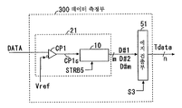
상술 데이터 천이 시간 정보 수집 수단(예를 들면, 데이터 측정부(300))의 일 양태는, 타이밍 정보 T1을 생성하는 아날로그 비교기와 다상 스트로브 수단(10)과 제1 에지 검출부와 제2 에지 검출부와 멀티플렉서(350)를 구비하고,One aspect of the above-described data transition time information collecting means (for example, the data measuring unit 300) includes an analog comparator for generating the timing information T1, a
아날로그 비교기는 DUT로부터 출력되는 비차동 신호의 데이터 신호 DATA를 받아서 소정의 임계 레벨 Vref에서 논리 신호로 변환한 논리 신호를 다상 스트로브 수단(10)에 공급하는 것이며,The analog comparator receives a data signal DATA of a non-differential signal output from the DUT and supplies a logic signal obtained by converting the data signal DATA to a logic signal at a predetermined threshold level Vref to the polyphase strobe means 10,
다상 스트로브 수단(10)은 아날로그 비교기로부터의 논리 신호를 받아서, 미소 위상차를 부여한 복수 m의 다상 스트로브 신호를 내부에서 생성하고, 생성한 복수 m의 다상 스트로브 신호에 의해 논리 신호를 각각 샘플링한 복수 m비트의 홀드 신호 D#i (여기서 i=1∼m)를 출력하는 것이며,The multiphase strobe means 10 receives a logic signal from the analog comparator and generates a plurality of m multiphase strobe signals provided with micro-phase difference therein. The multiphase strobing means 10 generates a plurality of m And outputs a hold signal D # i of the bit (here, i = 1 to m)
제1 에지 검출부는 복수 m비트의 홀드 신호 D#i를 받아서, 상승 에지 방향을 선택하는 에지 선택 신호 S2에 기초하여 m비트 입력을 n비트 출력으로 인코딩 변환한 한쪽의 상승측의 타이밍 정보 Tdh를 출력하는 데이터 인코더이며,The first edge detection unit receives the hold signal D # i of a plurality of m bits and generates timing information Tdh of one rising side which is obtained by encoding conversion of the m-bit input into n-bit output based on the edge selection signal S2 for selecting the rising edge direction And outputting the encoded data,
제2 에지 검출부는 복수 m비트의 홀드 신호 D#i를 받아서, 하강 에지 방향을 선택하는 에지 선택 신호 S2에 기초하여 m비트 입력을 n비트 출력으로 인코딩 변환 한 다른 쪽의 하강측의 타이밍 정보 Tdl를 출력하는 데이터 인코더이며,The second edge detection unit receives the hold signal D # i of a plurality of m bits and outputs the timing information Tdl of the other side on which the m-bit input is encoded into the n-bit output based on the edge selection signal S2 for selecting the falling edge direction And outputs the data,
멀티플렉서(350)는 한쪽의 상승측의 타이밍 정보 Tdh와 다른 쪽의 하강측의 타이밍 정보 Tdl를 받아서 데이터 에지를 선택하는 데이터 에지 선택 신호 S3에 기초하여 어느 하나를 선택하여 데이터 변화점 정보 Tdata로서 출력하는 것을 특징으로 하는 상술한 반도체 시험 장치가 있다.The
다음에, 제8 해결 수단을 개시한다. 여기에서 도 12는 본 발명에 따른 해결 수단을 도시하고 있다.Next, an eighth solution means is disclosed. Here, Fig. 12 shows the solution means according to the invention.
상술 데이터 천이 시간 정보 수집 수단(예를 들면, 데이터 측정부(300))의 일 양태는 타이밍 정보 T1를 생성하는 아날로그 비교기와 다상 스트로브 수단(10)과 에지 검출부를 구비하고,One aspect of the above-described data transition time information collection means (for example, the data measurement unit 300) includes an analog comparator for generating the timing information T1, a
아날로그 비교기는 DUT로부터 출력되는 비차동 신호의 데이터 신호 DATA를 받아서 소정의 임계 레벨 Vref에서 논리 신호로 변환한 논리 신호를 다상 스트로브 수단(10)에 공급하는 것이며,The analog comparator receives a data signal DATA of a non-differential signal output from the DUT and supplies a logic signal obtained by converting the data signal DATA to a logic signal at a predetermined threshold level Vref to the polyphase strobe means 10,
다상 스트로브 수단(10)은 아날로그 비교기로부터의 논리 신호를 받아서, 미소 위상차를 부여한 복수 m의 다상 스트로브 신호를 내부에서 생성하고, 생성한 복수 m의 다상 스트로브 신호에 의해 논리 신호를 각각 샘플링한 복수 m비트의 홀드 신호 D#i를 출력하는 것이며,The multiphase strobe means 10 receives a logic signal from the analog comparator and generates a plurality of m multiphase strobe signals provided with micro-phase difference therein. The multiphase strobing means 10 generates a plurality of m Bit hold signal D # i,
에지 검출부는 복수 m비트의 홀드 신호 D#i를 받아서, 상승 에지 방향 또는 하강 에지 방향의 데이터 에지를 선택하는 데이터 에지 선택 신호 S3에 기초하여 m비트 입력을 n비트 출력으로 인코딩 변환한 데이터 변화점 정보 Tdata를 출력하는 데이터 인코더인 것을 특징으로 하는 상술한 반도체 시험 장치가 있다.The edge detection unit receives the hold signal D # i of a plurality of m bits and generates a data change point which is obtained by encoding the m-bit input into the n-bit output based on the data edge selection signal S3 for selecting the data edge in the rising edge direction or the falling edge direction. And a data encoder for outputting information Tdata.
다음에, 제9 해결 수단을 개시한다. 여기에서 도 3과 도 5는 본 발명에 따른 해결 수단을 도시하고 있다.Next, a ninth solution means is disclosed. 3 and 5 show the solution means according to the invention.
상술한 크로스포인트 산출 수단의 일 양태는 제1 천이 정보 측정 수단에서 얻어진 제1 타이밍 정보를 T1으로 하고, 제2 타이밍 정보를 T2로 하고, 제2 천이 정보 측정 수단에서 얻어진 제3 타이밍 정보를 T3로 하고, 제4 타이밍 정보를 T4로 했을 때, One aspect of the above-mentioned cross point calculating means is such that the first timing information obtained by the first transition information measuring means is T1, the second timing information is T2, the third timing information obtained by the second transition information measuring means is T3 And the fourth timing information is T4,
Tcross={(T2×T4)-(T1×T3)}/{(T2-T1)+(T4-T3)}Tcross = {(T2.times.T4) - (T1.times.T3)} / {(T2-T1) + (T4-T3)}
의 연산 처리를 한 크로스포인트 정보 Tcross를 생성하여 출력하는 것(예를 들면, 크로스포인트 산출부(200))인 것을 특징으로 하는 상술한 반도체 시험 장치가 있다.(For example, a cross point calculating section 200) for generating and outputting cross point information Tcross subjected to the arithmetic processing of the cross point information Tcross.
다음에, 제10 해결 수단을 개시한다. 여기에서 도 11은 본 발명에 따른 해결 수단을 도시하고 있다.Next, a tenth solution means is disclosed. Here, Fig. 11 shows the solution means according to the invention.
상술 크로스포인트 산출 수단의 일 양태는 데이터 변환용의 크로스포인트 변환 메모리(250)를 구비하고,One aspect of the above-mentioned cross point calculating means includes the cross
제1 천이 정보 측정 수단에서 얻어진 제1 타이밍 정보를 T1으로 하고, 제2 타이밍 정보를 T2로 하고, 제2 천이 정보 측정 수단에서 얻어진 제3 타이밍 정보를 T3로 하고, 제4 타이밍 정보를 T4로 했을 때,The first timing information obtained by the first transition information measuring means is T1, the second timing information is T2, the third timing information obtained by the second transition information measuring means is T3, and the fourth timing information is T4 When you do,
크로스포인트 변환 메모리(250)는 상술 연산 처리에 대응하는 크로스포인트 정보 Tcross를 미리 상기 메모리에 저장해 두고, 타이밍 정보 T1, T2, T3, T4의 데 이터를 어드레스 입력단에 공급하고, 상기 어드레스에 의해 판독된 판독 데이터를 크로스포인트 정보 Tcross로서 출력하는 것을 특징으로 하는 상술한 반도체 시험 장치가 있다.The cross
다음에, 제11 해결 수단을 개시한다. 여기에서 도 3은 본 발명에 따른 해결 수단을 도시하고 있다.Next, an eleventh solution means is disclosed. Here, Fig. 3 shows a solution according to the invention.
상술 위상차 산출 수단의 일 양태로서는, 크로스포인트 산출 수단으로부터의 크로스포인트 정보 Tcross와, 데이터 천이 시간 정보 수집 수단(예를 들면, 데이터 측정부(300))으로부터의 데이터 변화점 정보 Tdata를 받아서, 양 데이터의 차분을 산출한 상대적인 위상차 ΔT를 출력하거나, 또는 상기 위상차 ΔT에 대해서 소정의 오프셋량(오프셋 시간 Toffset)을 더 가산한 결과의 위상차 ΔT를 출력하는 것(예를 들면, 위상차 산출부(400))인 것을 특징으로 하는 상술한 반도체 시험 장치가 있다.As one aspect of the above-described phase difference calculating means, the cross point information Tcross from the cross point calculating means and the data change point information Tdata from the data transition time information collecting means (for example, the data measuring unit 300) Outputting a relative phase difference DELTA T that calculates the difference of data or outputting a phase difference DELTA T as a result of further adding a predetermined offset amount (offset time Toffset) to the phase difference DELTA T (for example, )). ≪ / RTI >
다음에, 제12 해결 수단을 개시한다. 여기에서 도 3은 본 발명에 따른 해결 수단을 도시하고 있다.Next, a twelfth solution means is disclosed. Here, Fig. 3 shows a solution according to the invention.
상술 양부 판정 수단의 일 양태로서는, 위상차 산출 수단으로부터의 상대적인 위상차 ΔT를 받아서, 상기 DUT의 양불 판정을 수행하는 소정의 최대 위상차Tmax로부터 최소 위상차 Tmin의 허용 범위내인지에 기초하여 DUT의 양부 판정을 수행하는 것(예를 들면, 양부 판정부(500))인 것을 특징으로 하는 상술한 반도체 시험 장치가 있다.As an aspect of the above-described good and good determining means, the relative phase difference DELTA T is received from the phase difference calculating means, and the positive / negative determination of the DUT is made based on whether the predetermined maximum phase difference Tmax is within the allowable range of the minimum phase difference Tmin (For example, the positive / negative determination section 500).
다음에, 제13 해결 수단을 개시한다. 여기에서 도 10은 본 발명에 따른 해 결 수단을 도시하고 있다.Next, a thirteenth solution means is disclosed. Here, Fig. 10 shows the solution means according to the invention.
상술 크로스포인트 산출 수단과 양부 판정 수단에 대해서 양부 판정 제어 수단을 추가하여 구비하고,The above-mentioned cross-point calculating means and the above-mentioned correcting means are additionally provided,
양부 판정 제어 수단은 상기 천이 정보 측정 수단(예를 들면, 제1 천이 시간 정보 수집 수단(100#1), 제2 천이 시간 정보 수집 수단(100#2))으로부터 출력되는 4점의 제1 타이밍 정보 T1, 제2 타이밍 정보 T2, 제3 타이밍 정보 T3, 제4 타이밍 정보 T4 중 적어도 어느 하나의 데이터 값이 '0'일 때는, 정상적인 크로스포인트가 측정되지 않은 것으로 하여 데이터 에러 신호 Derr를 크로스포인트 산출 수단으로부터 발생시키고, 양부 판정 수단은 상기 데이터 에러 신호 Derr를 받았을 때에는 양부 판정을 수행하지 않도록 내부 제어하는 수단을 구비하는 것을 특징으로 하는 상술한 반도체 시험 장치가 있다.The positive decision control means is provided with a first timing of four points output from the transition information measuring means (for example, the first transition time information collecting means 100 # 1 and the second transition time information collecting means 100 # 2) When the data value of at least one of the information T1, the second timing information T2, the third timing information T3 and the fourth timing information T4 is '0', it is determined that the normal cross point is not measured and the data error signal Derr is cross- And the means for judging whether or not the data error signal Derr has been received is provided from the calculating means.
다음에, 제14 해결 수단을 개시한다. 여기에서 도 9는 본 발명에 따른 해결 수단을 도시하고 있다.Next, a fourteenth solution means is disclosed. Here, Fig. 9 shows the solution means according to the invention.
상기 과제를 해결하기 위하여, 피시험 디바이스로부터 출력되는 차동 출력 신호의 크로스포인트의 타이밍을 기준으로 하여, DUT로부터 출력되는 다른 데이터 신호 DATA와의 사이의 상대적인 위상차를 양호한 정밀도로 측정하는 것이 요구되는 반도체 시험 장치에 있어서,In order to solve the above problems, there is a semiconductor test in which it is required to measure the relative phase difference between the differential output signal output from the DUT and the other data signal DATA output from the DUT with good precision, based on the timing of the cross point of the differential output signal outputted from the DUT In the apparatus,
소정의 로우 레벨과 하이 레벨의 2포인트의 임계 레벨에서 논리 신호로 변환한 후, 이미 알려진 타이밍의 다상 스트로브 신호에 기초하여 샘플링 측정하여 코드 데이터로 변환한 제1 타이밍 정보 T1와 제2 타이밍 정보 T2를 출력하는 제1 천 이 정보 측정 수단(예를 들면, 제1 천이 시간 정보 수집 수단(100#1))을 구비하고,The first timing information T1 and the second timing information T2, which have been converted into the code data by the sampling measurement based on the polyphase strobe signal of known timing and converted into the code data, are converted into the logic signals at the two threshold levels of the predetermined low level and high level, (For example, the first transition time information collecting means 100 # 1) for outputting the first transition time information,
차동 출력 신호의 다른쪽의 신호의 천이 파형에 대하여, 크로스포인트를 발생시키는 소정의 하이 레벨과 로우 레벨의 2포인트의 임계 레벨에서 논리 신호로 변환한 후, 이미 알려진 타이밍의 다상 스트로브 신호에 기초하여 샘플링 측정하여 코드 데이터로 변환한 제3 타이밍 정보 T3와 제4 타이밍 정보 T4를 출력하는 제2 천이 정보 측정 수단(예를 들면, 제2 천이 시간 정보 수집 수단(100#2))을 구비하고,A logic level conversion circuit for converting a logic level of a transition waveform of the other signal of the differential output signal into a logic level at a predetermined high level and a low level at two threshold levels for generating a cross point, (For example, second transition time information collecting means 100 # 2) for outputting third timing information T3 and fourth timing information T4 obtained by sampling measurement and converted into code data,
DUT로부터 출력되는 데이터 신호 DATA를 받아서, 소정의 임계 레벨 Vref에서 논리 신호로 변환한 후, 이미 알려진 타이밍의 다상 스트로브 신호에 기초하여 샘플링 측정하여 데이터 신호 DATA의 상승 또는 하강의 타이밍을 나타내는 코드 데이터로 변환한 데이터 변화점 정보 Tdata를 출력하는 데이터 천이 시간 정보 수집 수단(예를 들면, 데이터 측정부(300))을 구비하고,The data signal DATA output from the DUT is converted into a logic signal at a predetermined threshold level Vref and then subjected to sampling measurement based on a polyphase strobe signal at a known timing to generate code data indicating the timing of the rise or fall of the data signal DATA And a data transition time information collection means (for example, a data measurement unit 300) for outputting the converted data change point information Tdata,
제1 천이 정보 측정 수단에서 측정한 2점의 타이밍 정보와, 제2 천이 정보 측정 수단에서 측정한 2점의 타이밍 정보와, 데이터 천이 시간 정보 수집 수단에서 측정한 1점의 타이밍 정보를 소정 복수회 측정하여 저장하는, 소정 저장 용량을 구비하는 에지 데이터 저장 수단(예를 들면, 에지 데이터 저장 메모리(700))를 구비하고,The timing information of two points measured by the first transition information measuring means, the timing information of two points measured by the second transition information measuring means, and the timing information of one point measured by the data transition time information collecting means, (For example, edge data storage memory 700) having a predetermined storage capacity for storing the measured and stored data,
에지 데이터 저장 수단의 데이터 내용을 판독하여, 소프트적으로 크로스포인트를 연산하여 산출한 크로스포인트 정보 Tcross와 데이터 변화점 정보 Tdata의 상대적인 위상차 ΔT를 연산하여 산출하고, 상기 연산 처리를 측정 회수에 대응한 회 수 수행하고, 얻어진 복수점의 위상차 ΔT에 대해서 상기 DUT 품종에 대한 위상차의 규격내인지 아닌지의 양부 판정을 수행하는 크로스포인트 산출·양부 판정 처리 수단(예를 들면, 크로스포인트 산출/위상차 산출/양부 판정 처리부(650))을 구비하며, 이상을 구비하는 것을 특징으로 하는 반도체 시험 장치가 있다.The data content of the edge data storage means is read and the relative phase difference? T between the cross point information Tcross and the data change point information Tdata calculated by calculating the cross point in software is calculated and calculated, (For example, a cross point calculation / phase difference calculation / phase difference calculation processing) for determining whether or not the obtained phase difference? T of the plurality of points is within the standard of the phase difference for the DUT type, And a positive / negative determination processing unit (650)), and has the above-described configuration.
다음에, 제15 해결 수단을 개시한다. 여기에서 도 9는 본 발명에 따른 해결 수단을 도시하고 있다.Next, a fifteenth solution means is disclosed. Here, Fig. 9 shows the solution means according to the invention.
상술한 반도체 시험 장치에 있어서, 상기 크로스포인트 산출·양부 판정 처리 수단에서 구한 측정 회수에 대응한 복수점의 위상차 ΔT를 받아서, 복수점의 위상차 ΔT의 변동량을 구하여 양 신호간에서의 지터량을 특정하는 기능을 추가하여 구비하는 것을 특징으로 하는반도체 시험 장치가 있다.In the semiconductor testing apparatus described above, a plurality of points of phase difference DELTA T corresponding to the number of measurements obtained by the cross point calculation and positive / negative determination processing means are received, and the amount of fluctuation of the phase difference DELTA T at a plurality of points is obtained. The semiconductor testing apparatus further includes a function of adding a function for testing the semiconductor device.
이에 따라, 양 신호간의 상대적인 지터량을 측정할 수 있다.Thus, the relative amount of jitter between both signals can be measured.
또한, 본 발명은 원하는 바에 따라 상기 해결 수단에서의 각 요소 수단을 적절히 조합하여, 실용 가능한 다른 구성 수단으로 해도 된다. 또한, 상기 각 요소에 부여되어 있는 부호는 발명의 실시 형태 등에 개시되어 있는 부호에 대응하지만, 이에 한정되는 것은 아니고, 실용 가능한 다른 균등물을 적용한 구성 수단으로 해도 된다.Further, the present invention may be applied to other constituent means that are practically usable by suitably combining the respective element means in the solution means as desired. The numerals given to the respective elements correspond to the numerals disclosed in the embodiments of the present invention and the like, but the present invention is not limited thereto, and constituent means using other practically usable equivalents may be used.
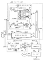
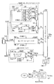
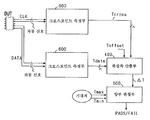
도 1은 DUT로부터 출력되는 차동 클럭 신호와 싱글 엔드의 데이터 신호 DATA를 받아서 양자의 상대적인 위상차를 구하여 양부 판정을 수행하는 경우의 반도체 시험 장치의 요부 블록 구성예이다.FIG. 1 is a block diagram showing a configuration of a main part of a semiconductor testing apparatus in a case where a differential clock signal outputted from a DUT and a single-ended data signal DATA are received and a relative phase difference between the differential clock signal and a differential signal is obtained.
도 2는 m=4비트일 때의 에지 검출부의 인코딩예, 및 회로 구성예이다.2 is an example of encoding and an example of a circuit configuration of the edge detecting unit when m = 4 bits.
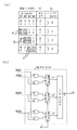
도 3은 크로스포인트 산출부(200)의 구체적인 내부 구성예이다.3 is a specific internal configuration example of the cross
도 4는 스트로브 신호 STRB1∼STRB4가 동일한 기준 타이밍 T0에서 발생하는 경우로 한 타이밍 정보 T1∼T4, Tdh를 나타내는 간명한 타이밍도이다.Fig. 4 is a simplified timing chart showing the timing information T1 to T4, Tdh when the strobe signals STRB1 to STRB4 occur at the same reference timing TO.
도 5는 크로스포인트 정보 Tcross의 산출 설명도이다.5 is an explanatory diagram of calculation of cross-point information Tcross.
도 6은 회로 기판상 등에서 2개의 디바이스간에서, 차동 클럭에 동기한 고속의 데이터 전송을 수행하는 경우의 원리적인 회로 접속과, DUT로부터 출력되는 차동 클럭 신호인 정클럭 신호 CLKP, 부클럭 신호 CLKN의 각각의 신호를 받기 위하여, 싱글 엔드의 비교기 CP를 구비하는 구성의 반도체 시험 장치의 요부이다.6 shows a schematic circuit connection in case of performing high-speed data transfer in synchronism with a differential clock between two devices on a circuit board or the like, a positive clock signal CLKP as a differential clock signal output from the DUT, a negative clock signal CLKN End comparator CP in order to receive the respective signals of the comparator CP.
도 7은 이상적인 차동 신호인 경우의 크로스포인트와, 실제의 차동 신호예의 크로스포인트와, 차동 클럭 신호 CLK와 데이터 신호 DATA의 양 신호에 있어서 지터 요인 등에 수반하는 동상 변화와 역상 변화를 설명하는 도면이다.Fig. 7 is a diagram for explaining the in-phase variation and the reverse phase variation accompanying the jitter factor in the cross point in the case of the ideal differential signal, the cross point in the actual differential signal example, and both signals of the differential clock signal CLK and the data signal DATA .
도 8은 펄스폭이 좁은 경우의 예를 나타낸 타이밍도이다.8 is a timing chart showing an example of a case where the pulse width is narrow.
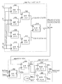
도 9는 DUT로부터 출력되는 차동 클럭 신호와 싱글 엔드의 데이터 신호 DATA를 받아서 양자의 상대적인 위상차를 구하여 양부 판정을 수행하는 경우의 반도체 시험 장치의, 다른 요부 블록 구성예이다.FIG. 9 shows another example of the main part block configuration of the semiconductor testing device in the case where the differential clock signal outputted from the DUT and the data signal DATA of the single end are received and the relative phase difference between them is obtained to perform the positive / negative judgment.
도 10은 DUT로부터 출력되는 차동 클럭 신호와 싱글 엔드의 데이터 신호 DATA를 받아서 양자의 상대적인 위상차를 구하여 양부 판정을 수행하는 경우의 반도체 시험 장치의, 또 다른 요부 블록 구성예이다.10 is another example of the configuration of the main part of the semiconductor testing apparatus in the case where the differential clock signal outputted from the DUT and the data signal DATA of the single end are received and the relative phase difference between the differential clock signal and the differential signal is obtained.
도 11은 DUT로부터 출력되는 차동 클럭 신호와 싱글 엔드의 데이터 신호 DATA를 받아서 양자의 상대적인 위상차를 구하여 양부 판정을 수행하는 경우의 반도체 시험 장치의, 또 다른 요부 블록 구성예이다.11 is another example of the configuration of a substantial block of the semiconductor testing apparatus in the case where the differential clock signal output from the DUT and the single-ended data signal DATA are received and the relative phase difference between them is obtained to perform the positive / negative determination.
도 12는 데이터 측정부(300)의 다른 구성예이다.FIG. 12 shows another configuration example of the data measuring unit 300. FIG.
도 13은 2계통의 차동 신호의 상대적인 위상차를 구하여 양부 판정을 수행하는 다른 구성예이다.Fig. 13 shows another configuration example in which the relative phase difference of the differential signals of the two systems is obtained to perform the positive / negative determination.
이하에 본 발명을 적용한 실시 형태의 일예를 도면을 참조하면서 설명한다. 또한, 이하의 실시 형태의 설명 내용에 의해 특허 청구의 범위를 한정하는 것은 아니며, 더욱이 실시의 형태에서 설명되어 있는 요소나 접속 관계 등이 해결 수단에 필수라고는 한정할 수 없다. 또한, 실시의 형태에서 설명되어 있는 요소나 접속 관계 등의 형용/형태는 일예로서 그 형용/형태 내용에만 한정하는 것은 아니다.BEST MODE FOR CARRYING OUT THE INVENTION Hereinafter, an embodiment of the present invention to which the present invention is applied will be described with reference to the drawings. Furthermore, the claims are not intended to limit the scope of the claims according to the following description of the embodiments, and the elements and connection relationships described in the embodiments can not necessarily be essential to the solution. In addition, the form / form of the element or the connection relationship described in the embodiment is not limited to the form / form content as an example.
본 발명에 대하여, 도 1∼도 13을 참조하여 이하에 설명한다.The present invention will be described below with reference to Figs.
도 1은 DUT로부터 출력되는 차동 클럭 신호와 싱글 엔드의 데이터 신호 DATA를 받아서 양자의 상대적인 위상차를 구하여 양부 판정을 수행하는 반도체 시험 장치의 요부 블록 구성예이다. 또한, 반도체 시험 장치의 전체 구성은 일본 특허출원 2000-178917호에 도시되어 있으므로 생략한다.FIG. 1 shows an example of the configuration of a main part of a semiconductor testing apparatus that receives a differential clock signal output from a DUT and a data signal DATA of a single end to obtain a relative phase difference between the two and determine whether the semiconductor test apparatus is correct. Further, the entire configuration of the semiconductor testing apparatus is shown in Japanese Patent Application No. 2000-178917, and will not be described here.
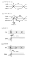
이 구성 요소는 제1 천이 시간 정보 수집 수단(100#1)과, 제2 천이 시간 정보 수집 수단(100#2)과, 제3 천이 시간 정보 수집 수단(100#3)과, 멀티플렉서(350)와, 크로스포인트 산출부(200)와, 위상차 산출부(400)와, 양부 판정부(500)를 구비한다. 또한, 데이터 측정부(300)는 상기 제3 천이 시간 정보 수집 수단(100#3)과 상기 멀티플렉서(350)의 구성 요소로 이루어진다.This component includes a first transition time information collection means 100 # 1, a second transition time information collection means 100 # 2, a third transition time information collection means 100 # 3, a
제1 천이 시간 정보 수집 수단(100#1)은 DUT로부터 출력되는 차동 클럭 신호의 하나의 정클럭 신호 CLKP를 받아서, 하이측과 로우측의 2점의 임계 레벨 VOH, VOL에서 논리 신호로 변환한 후, 논리 신호가 천이하기 전후의 타이밍 정보를 스트로브 신호 STRB2, STRB1에 기초하는 다상 STB에서 각각 측정하여, 시간 정보가 되는 코드 데이터로 변환한 타이밍 정보 T2, T1를 생성하여 출력하는 것이다. 이 내부 요소는 하이측 다상 스트로브 수단(21)과, 로우측 다상 스트로브 수단(22)과, 에지 검출부(51, 52)를 구비한다.The first transition time information collecting means 100 # 1 receives one positive clock signal CLKP of the differential clock signal output from the DUT and converts the one positive clock signal CLKP into a logic signal at the two threshold levels VOH and VOL on the high side and the low side The timing information before and after the transition of the logic signal is measured in the multi-phase STB based on the strobe signals STRB2 and STRB1, respectively, and the timing information T2 and T1 converted into the code data to be time information is generated and output. This internal element has high side polyphase strobing means 21, low side polyphase strobing means 22, and
하이측 다상 스트로브 수단(21)은 하이측의 임계 레벨 VOH에서 논리 신호로 변환한 논리 신호를 스트로브 신호 STRB2에 기초하는 다상 STB(다상 스트로브 신호)에 의한 m점의 개별 타이밍에서 샘플링한 결과의 m비트의 하이측 홀드 신호 HD#1∼HD#m를 출력하는 것이다. 내부 구성예로서는 비교기 CP2와, 다상 스트로브 수단(10)을 구비한다. 이에 대하여, 도 4의 타이밍 챠트를 참조하면서 설명한다. 또한, 도 4는 스트로브 신호 STRB1∼STRB4가 동일의 기준 타이밍 T0에서 발생하는 경우로 한 타이밍 정보 T1∼T4, Tdh를 나타내는 간명한 타이밍도이다.The high side polyphase strobing means 21 samples the logic signal converted into the logic signal at the high side threshold level VOH at the individual timing of the m point by the polyphase STB (polyphase strobe signal) based on the strobe signal STRB2, Bit high-side hold
다상 스트로브 수단(10)은 타이밍 발생기 TG(도시 생략)로부터의 하나의 스트로브 신호 STRB2를 받아서 시계열적으로 미소 지연하여 어긋나게 한 m점의 다상 STB(도 4의 A 참조)를 생성하고, 생성한 m점의 다상 STB에서, 비교기 CP2로부터 출력되는 논리 신호 CP2s를 m개의 타이밍 비교기 TC에서 각각 샘플링하고, 상기에서 샘플링한 결과의 m비트의 하이측 홀드 신호 HD#1∼HD#m을 출력하는 것이다. 여기 에서, m의 값은 예를 들면 16점/32점 등이 적용된다. 또한, 미소 지연량은 예를 들면 20피코초 피치가 적용된 경우, 32점×20피코초=640피코초의 구간에 걸쳐 연속한 미세한 피치의 시간 정보로서 취득할 수 있다. 한편으로, 스트로트 신호 STRB2 및 개개의 다상 STB는 캘리브레이션함으로써 이미 알려진 스트로브 타이밍으로 할 수 있다. 더욱이 스트로브 신호 STRB2는 임의의 타이밍으로 이동시켜 발생 억제할 수도 있다. 따라서, 도 4에 도시한 바와 같이, 유한 구간의 다상 STB이지만, 정클럭 신호 CLKP가 하이측의 임계 레벨 VOH 전후의 위치로 스트로브 신호 STRB2를 이동시켜 샘플링하는 것이 가능하다.The multi-phase strobe means 10 receives the one strobe signal STRB2 from the timing generator TG (not shown) and generates an m-point multi-phase STB (see Fig. 4A) In the multiphase STB of the point, the logic signals CP2s output from the comparator CP2 are sampled by the m timing comparators TC, respectively, and the m-bit high-side hold
에지 검출부(51)는 상승 또는 하강 에지의 선택 기능을 구비하며, m비트 입력을 n비트 출력으로 변환하는 데이터 인코더이다. 이에 대해서 도 2의 (a)의 m=4비트일 때의 에지 검출부의 인코딩예, 및 도 2의 (b)의 회로 구성예를 참조하면서 설명한다.The
도 2의 (a)에 있어서 첫째로, 에지 선택 신호 S2가 '0'일 때는 상승 에지를 대상으로 하여 인코딩한다. 입력 데이터가 '0111'인 시계열 데이터(도 2의 A 참조)일 때, 인코딩한 2비트의 코드 데이터 '1'로 변환하여 출력한다. 마찬가지로, 입력 데이터가 '0011'인 시계열 데이터(도 2의 B 참조)일 때, 코드 데이터 '2'를 출력한다. 마찬가지로, 입력 데이터가 '0001'인 시계열 데이터(도 2의 C 참조)일 때, 코드 데이터 '3'를 출력한다.In FIG. 2A, first, when the edge selection signal S2 is '0', the rising edge is encoded. When the input data is time series data (see A in FIG. 2) having '0111', it is converted into encoded 2-bit code data '1' and output. Likewise, when the input data is time series data (see FIG. 2B) having '0011', code data '2' is output. Likewise, when the input data is time series data (see C in FIG. 2) having the value '0001', the code data '3' is outputted.
둘째로, 에지 선택 신호 S2가 '1'일 때는 하강 에지를 대상으로 하여 인코딩한다. 상기와 마찬가지로 하여 입력 데이터가 '1000'인 시계열 데이터(도 2의 A 참조)일 때, 코드 데이터 '1'을 출력한다. 마찬가지로, 입력 데이터가 '1100'인 시계열 데이터(도 2의 B 참조)일 때, 코드 데이터 '2'를 출력한다. 마찬가지로, 입력 데이터가 '1110'인 시계열 데이터(도 2의 C 참조)일 때, 코드 데이터 '3'을 출력한다.Second, when the edge selection signal S2 is '1', the falling edge is encoded. In the same manner as described above, when the input data is time series data (see A in FIG. 2) having "1000", code data "1" is output. Similarly, when the input data is time series data (see FIG. 2B) of '1100', code data '2' is output. Likewise, when the input data is time series data (see C in FIG. 2) having "1110", code data "3" is output.
도 2의 (b)의 회로 구성예는 상기 동작을 실현하는 일예로서, 한쪽이 반전 입력단인 6개의 AND 게이트에서 시계열 데이터의 상승 변화 또는 하강 변화를 검출하여 출력하고, 3개 멀티플렉서와 에지 선택 신호 S2에 의해 상승 변화 또는 하강 변화의 어느 하나를 선택하여 출력하고, 이들 3비트의 검출 데이터를 우선순위 인코더(Priority Encoder)에서 2비트의 코드 데이터로 변환한 타이밍 정보 T2로서 출력한다.The circuit configuration example of FIG. 2 (b) is an example of realizing the above operation. In the circuit configuration example of FIG. 2 (b), one of the six AND gates as the inverting input terminal detects and outputs the rising or falling change of the time series data, S2, and outputs these 3-bit detected data as the timing information T2 obtained by converting a 2-bit code data from a priority encoder into a 2-bit code data.
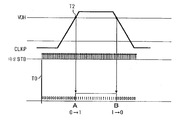
여기에서, 도 8의 펄스폭이 좁은 경우에 대해서 설명한다. 다상 STB 구간내에 있어서, 정클럭 신호 CLKP의 상승측과 하강측 모두가 존재하는 경우가 있다. 그러나, 에지 선택 신호 S2에 의해서 도 8의 A에 나타낸 상승 에지를 변환 대상으로 하거나, 도 8의 B에 나타낸 하강 에지를 변환 대상으로 하는지를 지정할 수 있으므로, 이와 같은 조건에 있어서도 목적의 코드 데이터를 지장없이 생성할 수 있다.Here, the case where the pulse width in Fig. 8 is narrow will be described. There are cases where both the rising side and the falling side of the positive clock signal CLKP exist in the polyphase STB section. However, it is possible to designate whether the rising edge shown in Fig. 8A is to be converted or the falling edge shown in Fig. 8B is to be converted by the edge selection signal S2. Therefore, even in such a condition, .
다음에, 도 1에 도시한 로우측 다상 스트로브 수단(22)은 상술한 하이측 다상 스트로브 수단(21)과 동일하므로, 로우측의 임계 레벨 VOL에서 논리 신호로 변환한 논리 신호를 스트로브 신호 STRB1에 기초한 다상 STB에 의한 m점의 개별 타이밍에서 샘플링한 결과의 m비트의 로우측 홀드 신호 LD#1∼LD#m를 출력하는 것이다. 또한, 스트로브 신호 STRB1와 상기 스트로브 신호 STRB2는 하나의 스트로브 신호로 공용해도 된다.Next, since the row side polyphase strobing means 22 shown in Fig. 1 is the same as the above-described high side polyphase strobing means 21, a logic signal converted into a logic signal at the threshold level VOL on the low side is input to the strobe signal STRB1 And outputs the m-bit low-side hold signals
에지 검출부(52)는 상술한 에지 검출부(51)와 동일하며, 상승 또는 하강 에지의 선택 기능을 구비하며, m비트 입력 n비트의 코드 데이터로 변환한 타이밍 정보 T1를 출력한다.The
제2 천이 시간 정보 수집 수단(100#2)은 상술한 제1 천이 시간 정보 수집 수단(100#1)과 동일하며, DUT로부터 출력되는 차동 클럭 신호의 다른 쪽의 부클럭 신호 CLKN을 받아서, 하이측과 로우측의 2점의 임계 레벨 VOH, VOL에서 논리 신호로 변환한 후, 스트로브 신호 STRB3, STRB4에 기초한 다상 STB에서 각각 측정하여, 시간 정보가 되는 코드 데이터로 변환한 타이밍 정보 T3, T4를 생성하여 출력한다.The second transition time information collecting means 100 # 2 is the same as the first transition time information collecting means 100 # 1 described above. The second transition time information collecting means 100 # 2 receives the other sub clock signal CLKN of the differential clock signal output from the DUT, Stage STB based on the strobe signals STRB3 and STRB4, and converts the timing information T3 and T4, which are converted into the code data serving as the time information, into the logic signals, respectively, from the threshold levels VOH and VOL at the two points And outputs it.
제3 천이 시간 정보 수집 수단(100#3)도 상술한 제1 천이 시간 정보 수집 수단(100#1)과 거의 동일하며, DUT로부터 출력되는 데이터 신호 DATA를 받아서 도 4 하측의 타이밍도에 도시한 바와 같이, 중간의 임계 레벨 Vref에서 논리 신호로 변환한 후, 스트로브 신호 STRB5, STRB6에 기초한 다상 STB에서 각각 측정하여, 시간 정보가 되는 코드 데이터로 변환한 타이밍 정보 Tdh, Tdl를 생성하여 출력한다. 이 때, 스트로브 신호 STRB5, STRB6측과, 스트로브 신호 STRB1∼STRB4측과는 기준 타이밍 T0에 대해서 도 4에 나타낸 오프셋 시간 Toffset가 존재하는 경우가 있다. 단, 이 오프셋 시간 Toffset은 각 스트로브 신호 STRB1∼STRB6가 이미 알려진 타이밍이므로, 이미 알려진 시간 정보이다.The third transition time information collecting means 100 # 3 is also substantially the same as the first transition time information collecting means 100 # 1 described above, and receives the data signal DATA output from the DUT, , The timing information Tdh and Tdl converted into the code data serving as time information are generated and output after being converted into the logic signal at the intermediate threshold level Vref and then measured at the multi-phase STB based on the strobe signals STRB5 and STRB6. At this time, the offset time Toffset shown in FIG. 4 may exist for the strobe signals STRB5 and STRB6 and for the strobe signals STRB1 to STRB4 with respect to the reference timing T0. However, this offset time Toffset is known time information since each of the strobe signals STRB1 to STRB6 is known timing.
또, 제3 천이 시간 정보 수집 수단(100#3)은 동일한 임계 레벨 Vref에서 논 리 신호로 변환하면 되므로, 이 내부 구성 요소는 도 1에 도시한 어느 하나의 다상 스트로브 수단(10)만을 구비하며, 이 출력 신호를 공용하여 에지 검출부(51)와 에지 검출부(52) 모두에게 공급하도록 구성해도 된다.Since the third transition time information collecting means 100 # 3 can be converted into a logical signal at the same threshold level Vref, this internal component includes only one of the polyphase strobing means 10 shown in FIG. 1 , And this output signal may be shared and supplied to both the
또한, 상기의 제3 천이 시간 정보 수집 수단(100#3)과 멀티플렉서(350)로 이루어지는 데이터 측정부(300)는 동일한 임계 레벨 Vref에서 논리 신호로 변환한 신호를 1계통의 다상 STB로 샘플링하면 되므로, 도 12의 데이터 측정부(300) 이외의 구성예로 도시한 바와 같이 구성 가능하다. 즉, 하이측 다상 스트로브 수단(21)과 에지 검출부(51)로 실현할 수 있다. 즉, 상술한 하나의 하이측 다상 스트로브 수단(21)에 있어서 임계 레벨 Vref에서 논리 신호로 변환하고, 이로부터 출력되는 홀드 신호 D#1∼D#m를 에지 검출부(51)에 공급하고, 데이터 에지 선택 신호 S3에 기초하여 선택한 상승측 에지 또는 하강측 에지의 데이터 변화점 정보 Tdata를 출력한다. 이 구성예에서는 보다 저렴하게 구성할 수 있다.When the data measuring unit 300 including the third transition time
도 1에 도시한 멀티플렉서(350)는 2입력 1출력형의 n비트폭의 데이터 셀렉터로서, 데이터 에지 선택 신호 S3에 의해, 상기 제3 천이 시간 정보 수집 수단(100#3)에서 생성한 상승 에지의 타이밍 정보 Tdh나, 하강 에지의 타이밍 정보 Tdl 중 어느 것을 선택한 결과의 데이터 변화점 정보 Tdata를 위상차 산출부(400)에 공급한다.The
크로스포인트 산출부(200)는 상술에서 얻은 정클럭 신호 CLKP측의 2점의 타이밍 정보 T1, T2와, 부클럭 신호 CLKN측의 2점의 타이밍 정보 T3, T4에 기초하여 크로스포인트를 산출하는 것이다. 이에 대해서 도 5의 크로스포인트 정보 Tcross 의 산출 설명도를 참조하면서 설명한다. 여기에서 타이밍 정보 T1 과 T2의 파형 구간, 및 타이밍 정보 T3 와 T4의 파형 구간에 있어서는, 대략 직선적으로 파형 변화하는 것으로 가정하여 산출한다.The cross
도 5의 (a)의 크로스포인트 정보 Tcross는 도 5의 (b)에 도시한 바와 같이, The cross-point information Tcross shown in FIG. 5 (a), as shown in FIG. 5 (b)
Tcross={(T2×T4)-(T1×T3)}/{(T2-T1)+(T4-T3)}Tcross = {(T2.times.T4) - (T1.times.T3)} / {(T2-T1) + (T4-T3)}
의 연산식으로부터 구할 수 있다.Can be obtained from the following expression.
또, 도 5의 (c)의 변칙적인 타이밍 정보 T1∼T4로 된 경우에 있어서도, 상기 연산식으로부터 구할 수 있다. 이로부터, 클럭이 천이하는 파형 구간 가운데에서, 직선적이 되는 원하는 파형 부분을 측정할 수 있음을 의미한다.Also, even in the case of the irregular timing information T1 to T4 in Fig. 5 (c), it can be obtained from the above equation. From this, it means that a desired waveform portion that is linear can be measured in a waveform section in which the clock transits.
도 3에 크로스포인트 산출부(200)의 구체적인 내부 구성예를 도시한다. 이 구성예에서는 상기 연산식에 대응하여, 2개의 승산기와, 3개의 감산기와, 1개의 가산기와, 1개의 제산기를 구비한다. 상기에서 연산한 결과의 데이터에서, 원하는 n비트의 크로스포인트 정보 Tcross를 위상차 산출부(400)에 공급한다. 그런데, 이들의 연산 시간은 수백 나노초 전후 걸리므로, DUT의 샘플링 측정의 주기도 이에 대응한 시간 이상의 주기로 측정을 수행한다. 또한, DUT의 특성에 따라서도 다르지만, 실용적으로는 예를 들면 수천회 이상의 샘플링 측정과 PASS/FAIL 판정을 반복하면, DUT의 평가를 실용적으로 수행할 수 있다.FIG. 3 shows a concrete internal configuration example of the cross
도 1에 도시한 위상차 산출부(400)는 차동 클럭 신호 CLK의 크로스포인트와, 데이터 신호 DATA의 양 신호에서의 상대적인 위상차 ΔT를 구하는 것이다, 즉, 상술에서 구한 크로스포인트 정보 Tcross와 데이터 변화점 정보 Tdata를 받아서, 양 자의 위상차 ΔT를 산출하여 양부 판정부(500)에 공급한다. 실제의 반도체 시험 장치의 측정에서는 개별 타이밍의 스트로브 신호가 사용되므로, 스트로브 신호간의 시간차인 오프셋 시간 Toffset을 부여한 위상차 ΔT를 산출한다. 따라서, 위상차 ΔT는, The
ΔT=(Tdata+Toffset)-Tcross DELTA T = (Tdata + Toffset) - Tcross
의 연산 처리를 수행한다. 또, 오프셋 시간 Toffset은 DUT 품종의 규격에 의존하여 다르므로, 정의 값, 부의 값, 또는 제로 값이 될 수 있다.. Since the offset time Toffset differs depending on the specification of the DUT varieties, it can be a positive value, a negative value, or a zero value.
양부 판정부(500)는 상기 DUT 품종에 대한 위상차의 규격내이면 PASS로서 판정하고, 범위 밖에 있으면 FAIL로서 판정하는 것이다. 즉, DUT의 규격인 최대 위상차 Tmax와 최소 위상차 Tmin에 기초하여, 상기에서 구한 위상차 ΔT를 비교하여, Tmin≤ΔT≤Tmax이면 PASS로서 판정하고, 그 이외는 FAIL로서 판정을 수행한다.The positive /
상술한 도 1의 발명 구성예에 따르면, 동일 측정 시각에서의 차동 클럭 신호 CLK의 크로스포인트를 특정하고, 상기 크로스포인트와 데이터 신호 DATA의 양 신호간의 위상차를 구하고, 구한 위상차가 소정의 규격내인지의 여부에 따라 양부 판정하는 수단을 구비하는 구성으로 함으로써, 차동 클럭 신호 CLK의 크로스포인트에 기초하여 양 신호의 상대적인 위상차를 적확하게 양부 판정할 수 있는 우수한 이점을 얻을 수 있다. 물론, 양 신호간에 있어서 순간적인 지터나 요동 등이 존재하더라도, 적확하게 양부 판정할 수 있다.According to the inventive configuration example of FIG. 1 described above, the cross point of the differential clock signal CLK at the same measurement time is specified, the phase difference between the cross point and the data signal DATA is found, and if the obtained phase difference is within a predetermined standard It is possible to obtain a superior advantage that the relative phase difference between both signals can be accurately judged based on the cross point of the differential clock signal CLK. Of course, even if there is instantaneous jitter or fluctuation between both signals, it is possible to judge whether or not the signal is correct.
또한, 본 발명의 기술적 사상은 상술 실시의 형태의 구체 구성예, 접속 형태예로 한정되는 것은 아니다. 또한, 본 발명의 기술적 사상에 기초하여 상술 실시 의 형태를 적절히 변형하여 광범위하게 응용해도 된다.The technical spirit of the present invention is not limited to the concrete configuration example of the above-described embodiment, and the connection form example. Further, the above-described embodiments may be suitably modified on the basis of the technical idea of the present invention to be widely applied.
상술한 도 1의 구성예에서는 차동 클럭 신호 CLK로 한 구체예에서 설명했으나, 클럭 신호 CLK 이외의 다른 차동 신호에도 적용할 수 있다.In the configuration example of FIG. 1 described above, the differential clock signal CLK has been described in the specific example, but it can also be applied to differential signals other than the clock signal CLK.
또한, 상술한 도 1 의 구성예에서는 1채널의 차동 클럭 신호 CLK와, 1채널의 데이터 신호 DATA로 한 신호 조건에서의 위상차를 시험하는 구체예로 설명했으나, 다른 신호 조건에 적용해도 된다. 첫번째 예로서는 도 13에 도시한 2계통의 차동 신호의 상대적인 위상차를 구하여 양부 판정을 수행하는 다른 구성예가 있다. 이는 2계통의 차동 신호의 양자간의 위상차를 시험할 수 있도록, 도 1에 도시한 크로스포인트 측정부(600)를 2계통 구비하는 구성으로 함으로써, 2계통의 차동 신호간의 위상차를 양부 판정할 수 있다. 두번째 예로서는, 도 1의 구성예에 나타낸 데이터 신호 DATA를 측정하는 데이터 측정부(300)를 복수 계통 구비하고, 이에 대응하는 위상차 산출부(400)와, 양부 판정부(500)로 함으로써, 복수 계통의 데이터 신호 DATA에 대해서 상대적인 위상차를 한번에 양부 판정할 수 있다.In the above-described configuration example of FIG. 1, a specific example of testing the phase difference under one signal condition using the differential clock signal CLK of one channel and the data signal DATA of one channel has been described. However, it may be applied to other signal conditions. As a first example, there is another configuration example in which the relative phase difference of the two systems of differential signals shown in Fig. This makes it possible to determine the phase difference between the differential signals of the two systems by providing two systems of the
또한, DUT의 디바이스 품종에 따라 다르지만, 시험 대상의 차동 클럭 신호 CLK 등의 차동 신호는 통상 1채널 또는 수채널 정도의 특정의 신호이므로, 반도체 시험 장치에 구비하는 상술 구성의 채널수는, DUT에 대응한 채널수를 구비하도록 구성하면 된다.Since the differential signal such as the differential clock signal CLK to be tested is usually a specific signal of about one channel or several channels, the number of channels of the above-described configuration provided in the semiconductor testing apparatus is different from that of the DUT It may be configured to have the corresponding number of channels.
또한, 1채널의 차동 클럭 신호 CLK와, 복수 채널의 데이터 신호 DATA를 동시에 시험하는 경우에는, 이에 대응하여 복수 채널의 데이터 측정부(300)와, 상기 복수 채널의 데이터 측정부(300)에 대응한 위상차 산출부(400)와 양부 판정부(500)를 구비하도록 구성할 수 있다.When a single-channel differential clock signal CLK and a plurality of channels of data signals DATA are tested at the same time, a plurality of channels of data measurement unit 300 and a plurality of channels of data measurement unit 300 A phase
또한, 상술한 도 1의 구성예에서는 전체를 회로로 실현한 구체예였으나, 이에 한정하지 않는다. 예를 들면, 도 9에 도시한 다른 구성예로도 실현 가능하다, 이는 도 1의 크로스포인트 산출부(200)와 위상차 산출부(400)와 양부 판정부(500)를 삭제하고, 대신에 에지 데이터 저장 메모리(700)와, 어드레스 발생부(620)와, 크로스포인트 산출/위상차 산출/양부 판정 처리부(650)를 추가하여 구비하는 구성예이다.In the above-described configuration example of Fig. 1, the entirety is a circuit, but the present invention is not limited thereto. For example, another configuration example shown in Fig. 9 can be realized. This is achieved by deleting the cross
에지 데이터 저장 메모리(700)는 원하는 용량의 메모리로서, 샘플링 측정의 각 시간, 타이밍 정보 T1∼T4, 및 데이터 변화점 정보 Tdata를 일괄하여 저장한다. 이로써, 다수회의 샘플링 측정 결과를 저장할 수 있다.The edge
어드레스 발생부(620)는 메모레에의 어드레스 발생용으로서, 샘플링 측정의 각 시간, INC 신호에 의해 어드레스 값을 +1한 어드레스 신호를 발생하여 에지 데이터 저장 메모리(700)에 공급한다.The
크로스포인트 산출/위상차 산출/양부 판정 처리부(650)는 소프트적으로 크로스포인트를 산출하여 판정하는 것으로서, 상기 에지 데이터 저장 메모리(700)에 저장된 에지 데이터를 순차 판독하여, 도 1의 구성예와 마찬가지로 하여, 소프트적으로 크로스포인트 정보 Tcross를 산출하고, 소프트적으로 위상차 ΔT를 산출하고, 기대치의 최대 위상차 Tmax와 최소 위상차 Tmin에 기초하여 위상차 ΔT의 양부 판정 처리를 수행하여, PASS/FAIL의 판정 결과를 출력한다.The cross-point calculation / phase-difference calculation / positive / negative
이에 따르면, 도 1의 구성예보다도 회로 규모를 저감할 수 있는 이점을 얻을 수 있다. This makes it possible to obtain an advantage that the circuit scale can be reduced as compared with the configuration example of Fig.
또한, 도 3에 도시한 크로스포인트 산출부(200)에 있어서, 원하는 바에 따라 클럭에 동기하여 연산하는 파이프 라인 회로 구성이나 인터리브 구성을 구비해도 된다. 이 경우에는, 반복 샘플링 측정하는 샘플링 주기를 대폭으로 단축할 수 있다.The cross-point calculating
또한, 도 11에 다른 구성예를 도시한다, 이는 상술한 도 1 구성의 크로스포인트 산출부(200) 대신에, 데이터 변환용의 크로스포인트 변환 메모리(250)를 구비하는 구성예이다. 크로스포인트 변환 메모리(250)는 타이밍 정보 T1∼T4의 입력 데이터를 어드레스 입력단에 공급하고, 이에 따라 지정된 어드레스의 내용을 판독하여 크로스포인트 정보 Tcross로서 출력한다. n=5비트인 경우, 5×4=20비트의 어드레스 공간의 메모리(RAM/ROM)를 구비한다. 여기에서, 메모리의 내용은 상술한 크로스포인트 정보 Tcross가 판독되도록, 미리 저장하여 구비해 둔다. 이에 의해서도, 상술한 크로스포인트 산출부(200)와 같은 기능을 실현할 수 있다.11 shows another configuration example. This configuration is an example of a configuration including the cross
또한, 도 10에 다른 구성예를 도시한다. 이는 상술한 도 1 구성의 크로스포인트 산출부(200)과 양부 판정부(500)을, 크로스포인트 산출부(201)과 양부 판정부(501)로 변경한 구성이다. 크로스포인트 산출부(201)은 입력되는 타이밍 정보 T1∼T4 중 어느 것이 '0'인 경우에는 크로스포인트가 검출되지 않았으므로, 정상적인 위치에서 샘플링 측정할 수 없었던 것으로 하여 데이터 에러 신호 Derr를 발생시킨다. 양부 판정부(501)은 상기 데이터 에러 신호 Derr를 받았을 때는 양부 판정을 수행하지 않도록 내부 제어한다.
Fig. 10 shows another configuration example. This is a configuration in which the cross
이에 따르면, 정상적인 위치에서 샘플링 측정이 이루어졌을 때에만 양부 판정이 수행되는 결과, 예를 들면 차동 클럭 신호 CLK와 반도체 시험 장치의 시험 주기(테스트 레이트)가 비동기 관계인 경우이거나, 차동 클럭 신호 CLK의 클럭 주파수가 큰 요동을 가지는 경우이더라도, 일정의 확률 빈도로 정상적으로 샘플링 측정할 수 있으므로, 정상적으로 샘플링 측정할 수 있었을 때에 적확한 양부 판정이 가능한 큰 이점을 얻을 수 있다.For example, when the differential clock signal CLK and the test period (test rate) of the semiconductor testing apparatus are asynchronous, or when the differential clock signal CLK is synchronized with the differential clock signal CLK, Even when the frequency has a large fluctuation, the sampling measurement can be performed normally at a certain probability frequency, so that it is possible to obtain a great advantage that a good judgment can be made when the sampling measurement can be normally performed.
또한, 상술 구성 요소 또는 실현하는 기능 수단에 대해서 실용적으로 적용 가능한 부위에 대해서는, 소프트웨어 또는 마이크로프로그램과 하드웨어 로직 양쪽에 기초하여 실현하는 구성 수단으로 해도 되고, 소프트웨어에 기초하여 실현하는 구성 수단으로 해도 된다.In addition, as for the parts that can be practically applied to the above-mentioned constituent elements or the functional means to be realized, the constituent elements may be realized by software or by both microprograms and hardware logic, or may be realized by software .
본 발명은 상술의 설명 내용으로부터, 하기에 기재되는 효과를 갖는다.The present invention has the effects described below from the above description.
상기 설명한 바와 같이 본 발명에 따르면, 동일 측정 시각에 있어서의 차동 클럭 신호 CLK의 크로스포인트를 특정하고, 상기 크로스포인트와 데이터 신호 DATA의 양 신호간의 위상차를 구하고, 구한 위상차가 소정의 규격내인지의 여부에 따라 양부 판정하는 수단을 구비하는 구성으로 함으로써, 차동 클럭 신호 CLK의 크로스포인트에 기초하여 양 신호의 상대적인 위상차를 적확하게 양부 판정할 수 있는 우수한 이점을 얻을 수 있다.As described above, according to the present invention, the cross point of the differential clock signal CLK at the same measurement time is specified, the phase difference between the signal of the cross point and the signal of the data signal DATA is obtained, It is possible to obtain a superior advantage that the relative phase difference between both signals can be accurately judged based on the cross point of the differential clock signal CLK.
또한 도 10의 구성예에 따르면, 정상적인 위치에서 샘플링 측정이 이루어졌을 때에만 양부 판정이 이루어지는 결과, 차동 클럭 신호 CLK와 반도체 시험 장치 의 시험 주기(테스트 레이트)가 비동기 관계인 경우이더라도, 적정하게 샘플링 측정된 측정 결과에 기초하여 적확한 양부 판정을 할 수 있는 이점을 얻을 수 있다.According to the configuration example of FIG. 10, even when the differential clock signal CLK and the test cycle (test rate) of the semiconductor test apparatus are in an asynchronous relationship as a result of judging only when the sampling measurement is performed at the normal position, It is possible to obtain an advantage of making an appropriate judgment based on the measurement result.
따라서, 본 발명의 기술적 효과는 크며, 산업상의 경제 효과도 크다. Therefore, the technical effect of the present invention is large, and the industrial economic effect is great.
Claims (10)
Applications Claiming Priority (3)
| Application Number | Priority Date | Filing Date | Title |
|---|---|---|---|
| JP2002168304 | 2002-06-10 | ||
| JPJP-P-2002-00168304 | 2002-06-10 | ||
| PCT/JP2003/007315 WO2003104826A1 (en) | 2002-06-10 | 2003-06-10 | Semiconductor test apparatus |
Publications (2)
| Publication Number | Publication Date |
|---|---|
| KR20050007601A KR20050007601A (en) | 2005-01-19 |
| KR101035184B1 true KR101035184B1 (en) | 2011-05-17 |
Family
ID=29727683
Family Applications (1)
| Application Number | Title | Priority Date | Filing Date |
|---|---|---|---|
| KR1020047020030A KR101035184B1 (en) | 2002-06-10 | 2003-06-10 | Semiconductor test apparatus |
Country Status (4)
| Country | Link |
|---|---|
| US (2) | US7126366B2 (en) |
| JP (2) | JP4628096B2 (en) |
| KR (1) | KR101035184B1 (en) |
| WO (1) | WO2003104826A1 (en) |
Families Citing this family (18)
| Publication number | Priority date | Publication date | Assignee | Title |
|---|---|---|---|---|
| DE10029536A1 (en) * | 2000-06-15 | 2001-12-20 | Bosch Gmbh Robert | Handgrip for a portable power tool has an elastic vibration damper at the mounting to the tool housing to prevent vibrations through the handle and maintain a mounting at the tool housing if the damper is damaged |
| KR100942104B1 (en) * | 2002-12-20 | 2010-02-12 | 가부시키가이샤 어드밴티스트 | Semiconductor test instrument |
| US20060267605A1 (en) * | 2005-05-27 | 2006-11-30 | Yang Kei-Wean C | Differential measurement probe having a ground clip system for the probing tips |
| US7346880B2 (en) * | 2005-06-30 | 2008-03-18 | Intel Corporation | Differential clock ganging |
| JP4895551B2 (en) * | 2005-08-10 | 2012-03-14 | 株式会社アドバンテスト | Test apparatus and test method |
| WO2007032061A1 (en) * | 2005-09-13 | 2007-03-22 | Advantest Corporation | Manufacturing system, manufacturing method, management device, managing method, and program |
| DE112006003595T5 (en) * | 2005-12-28 | 2008-11-13 | Advantest Corporation | Tester, test method and program |
| US7671602B1 (en) * | 2007-01-24 | 2010-03-02 | Integrated Device Technology, Inc. | Method and apparatus for cross-point detection |
| US7783452B2 (en) | 2007-03-08 | 2010-08-24 | Advantest Corporation | Signal measurement apparatus and test apparatus |
| US7797121B2 (en) * | 2007-06-07 | 2010-09-14 | Advantest Corporation | Test apparatus, and device for calibration |
| US7834615B2 (en) * | 2007-07-02 | 2010-11-16 | Texas Instruments Incorporated | Bist DDR memory interface circuit and method for self-testing the same using phase relationship between a data signal and a data strobe signal |
| US7756654B2 (en) * | 2007-08-15 | 2010-07-13 | Advantest Corporation | Test apparatus |
| JP5446112B2 (en) * | 2008-03-31 | 2014-03-19 | 富士通セミコンダクター株式会社 | Semiconductor device and method for monitoring operation of semiconductor device |
| US8456170B2 (en) * | 2008-05-09 | 2013-06-04 | Advantest Corporation | Test apparatus for digital modulated signal |
| JP5359570B2 (en) * | 2009-06-03 | 2013-12-04 | 富士通株式会社 | Memory test control apparatus and memory test control method |
| JP2014017807A (en) * | 2012-06-11 | 2014-01-30 | Denso Corp | Semiconductor device |
| JP2014109453A (en) * | 2012-11-30 | 2014-06-12 | Renesas Electronics Corp | Semiconductor device |
| US9891277B2 (en) * | 2014-09-30 | 2018-02-13 | Nxp Usa, Inc. | Secure low voltage testing |
Citations (2)
| Publication number | Priority date | Publication date | Assignee | Title |
|---|---|---|---|---|
| KR20010076307A (en) * | 2000-01-18 | 2001-08-11 | 오우라 히로시 | Method and apparatus for testing semiconductor devices |
| US20020003433A1 (en) | 2000-07-06 | 2002-01-10 | Takahiro Housako | Method and apparatus for testing semiconductor devices |
Family Cites Families (7)
| Publication number | Priority date | Publication date | Assignee | Title |
|---|---|---|---|---|
| JP3331109B2 (en) * | 1996-01-23 | 2002-10-07 | 株式会社アドバンテスト | Semiconductor test equipment comparator |
| JPH1138086A (en) * | 1997-07-16 | 1999-02-12 | Advantest Corp | Semiconductor test device |
| JP4495308B2 (en) | 2000-06-14 | 2010-07-07 | 株式会社アドバンテスト | Semiconductor device testing method and semiconductor device testing equipment |
| JP4394789B2 (en) | 2000-01-18 | 2010-01-06 | 株式会社アドバンテスト | Semiconductor device testing method and semiconductor device testing equipment |
| WO2001095075A1 (en) * | 2000-06-02 | 2001-12-13 | Hitachi,Ltd | Semiconductor integrated circuit and clock distribution circuit |
| JP4443728B2 (en) * | 2000-06-09 | 2010-03-31 | 株式会社ルネサステクノロジ | Clock generation circuit |
| JP4429625B2 (en) * | 2003-04-25 | 2010-03-10 | 株式会社アドバンテスト | Measuring apparatus and program |
-
2003
- 2003-06-10 WO PCT/JP2003/007315 patent/WO2003104826A1/en active Application Filing
- 2003-06-10 JP JP2004511845A patent/JP4628096B2/en not_active Expired - Fee Related
- 2003-06-10 US US10/516,093 patent/US7126366B2/en not_active Expired - Fee Related
- 2003-06-10 KR KR1020047020030A patent/KR101035184B1/en active IP Right Grant
-
2006
- 2006-07-14 US US11/486,825 patent/US7332926B2/en active Active
-
2010
- 2010-01-18 JP JP2010008199A patent/JP4977217B2/en not_active Expired - Fee Related
Patent Citations (4)
| Publication number | Priority date | Publication date | Assignee | Title |
|---|---|---|---|---|
| KR20010076307A (en) * | 2000-01-18 | 2001-08-11 | 오우라 히로시 | Method and apparatus for testing semiconductor devices |
| US20010052097A1 (en) | 2000-01-18 | 2001-12-13 | Advantest Corporation | Method and apparatus for testing semiconductor devices |
| KR100432965B1 (en) | 2000-01-18 | 2004-05-28 | 가부시키가이샤 아드반테스트 | Method and apparatus for testing semiconductor devices |
| US20020003433A1 (en) | 2000-07-06 | 2002-01-10 | Takahiro Housako | Method and apparatus for testing semiconductor devices |
Also Published As
| Publication number | Publication date |
|---|---|
| US20050231227A1 (en) | 2005-10-20 |
| KR20050007601A (en) | 2005-01-19 |
| US7126366B2 (en) | 2006-10-24 |
| WO2003104826A1 (en) | 2003-12-18 |
| US20070024311A1 (en) | 2007-02-01 |
| JP2010096770A (en) | 2010-04-30 |
| US7332926B2 (en) | 2008-02-19 |
| JP4628096B2 (en) | 2011-02-09 |
| JP4977217B2 (en) | 2012-07-18 |
| JPWO2003104826A1 (en) | 2005-10-06 |
Similar Documents
| Publication | Publication Date | Title |
|---|---|---|
| JP4977217B2 (en) | Semiconductor test equipment | |
| KR100997086B1 (en) | Jitter measuring instrument and tester | |
| KR100432965B1 (en) | Method and apparatus for testing semiconductor devices | |
| US7574632B2 (en) | Strobe technique for time stamping a digital signal | |
| US7474974B2 (en) | Embedded time domain analyzer for high speed circuits | |
| KR101243627B1 (en) | Time measurement using phase shifted periodic waveforms | |
| US7856578B2 (en) | Strobe technique for test of digital signal timing | |
| US7355387B2 (en) | System and method for testing integrated circuit timing margins | |
| JP5254794B2 (en) | Strobe technique for testing the timing of digital signals | |
| KR100269704B1 (en) | Apparatus for testing delay circuit and integrated circuit including means for testing the same | |
| JP4495308B2 (en) | Semiconductor device testing method and semiconductor device testing equipment | |
| CN100422756C (en) | Semiconductor test device | |
| JP2001201532A (en) | Method and apparatus for testing semiconductor device | |
| US7197682B2 (en) | Semiconductor test device and timing measurement method | |
| US20110181298A1 (en) | Measurement apparatus and test apparatus | |
| US20030210032A1 (en) | Jitter quantity calculator and tester | |
| KR102198916B1 (en) | Apparatus for Measuring Signal Delay for Semiconductor Test and Apparatus for Test using Same | |
| WO2011033588A1 (en) | Testing apparatus and testing method | |
| KR100429633B1 (en) | Boundary Scan Test System and Method for the Same | |
| JP2014130095A (en) | Testing device and testing method |
Legal Events
| Date | Code | Title | Description |
|---|---|---|---|
| A201 | Request for examination | ||
| E902 | Notification of reason for refusal | ||
| E902 | Notification of reason for refusal | ||
| E701 | Decision to grant or registration of patent right | ||
| GRNT | Written decision to grant | ||
| FPAY | Annual fee payment |
Payment date: 20140418 Year of fee payment: 4 |
|
| FPAY | Annual fee payment |
Payment date: 20150424 Year of fee payment: 5 |
|
| FPAY | Annual fee payment |
Payment date: 20160425 Year of fee payment: 6 |
|
| FPAY | Annual fee payment |
Payment date: 20170427 Year of fee payment: 7 |
|
| FPAY | Annual fee payment |
Payment date: 20180425 Year of fee payment: 8 |
|
| FPAY | Annual fee payment |
Payment date: 20190425 Year of fee payment: 9 |