KR100720122B1 - 반도체 웨이퍼 검사기의 프로브 장치 - Google Patents
반도체 웨이퍼 검사기의 프로브 장치 Download PDFInfo
- Publication number
- KR100720122B1 KR100720122B1 KR1020050026480A KR20050026480A KR100720122B1 KR 100720122 B1 KR100720122 B1 KR 100720122B1 KR 1020050026480 A KR1020050026480 A KR 1020050026480A KR 20050026480 A KR20050026480 A KR 20050026480A KR 100720122 B1 KR100720122 B1 KR 100720122B1
- Authority
- KR
- South Korea
- Prior art keywords
- circuit board
- wafer
- probe card
- vertical circuit
- probe
- Prior art date
- Legal status (The legal status is an assumption and is not a legal conclusion. Google has not performed a legal analysis and makes no representation as to the accuracy of the status listed.)
- Expired - Fee Related
Links
Images


Classifications
-
- G—PHYSICS
- G01—MEASURING; TESTING
- G01R—MEASURING ELECTRIC VARIABLES; MEASURING MAGNETIC VARIABLES
- G01R1/00—Details of instruments or arrangements of the types included in groups G01R5/00 - G01R13/00 and G01R31/00
- G01R1/02—General constructional details
- G01R1/06—Measuring leads; Measuring probes
- G01R1/067—Measuring probes
- G01R1/073—Multiple probes
- G01R1/07307—Multiple probes with individual probe elements, e.g. needles, cantilever beams or bump contacts, fixed in relation to each other, e.g. bed of nails fixture or probe card
- G01R1/07314—Multiple probes with individual probe elements, e.g. needles, cantilever beams or bump contacts, fixed in relation to each other, e.g. bed of nails fixture or probe card the body of the probe being perpendicular to test object, e.g. bed of nails or probe with bump contacts on a rigid support
-
- G—PHYSICS
- G01—MEASURING; TESTING
- G01R—MEASURING ELECTRIC VARIABLES; MEASURING MAGNETIC VARIABLES
- G01R31/00—Arrangements for testing electric properties; Arrangements for locating electric faults; Arrangements for electrical testing characterised by what is being tested not provided for elsewhere
- G01R31/26—Testing of individual semiconductor devices
- G01R31/2601—Apparatus or methods therefor
Landscapes
- Physics & Mathematics (AREA)
- General Physics & Mathematics (AREA)
- Testing Or Measuring Of Semiconductors Or The Like (AREA)
Abstract
Description
Claims (8)
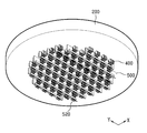
- 마더보드(100)의 중앙에 배열된 커넥터들(300)과,커넥터(300)들을 통해 상기 마더보드(100)의 하부에 전기적으로 연결된 프로브카드(200)와,상기 커넥터(300)와 교차되는 방향으로 배열되어 상기 프로브카드(200)의 하부 중앙에 통전가능하게 부착된 소켓(400)들과,상기 소켓(400)들을 통해 프로브카드(200)와 분리가능하게 통전결합되며 하단에 웨이퍼칩(3a)의 패드(3b)에 접촉되는 접촉핀(520)들이 다수형성된 수직회로기판(500)을 포함하여 구성된 것을 특징으로 하는 반도체 웨이퍼 검사기의 프로브 장치.
- 삭제
- 제 1항에 있어서,상기 소켓(400)은프로브카드(200)의 하부에 수직으로 부착되는 박판으로서, 수직회로기판(500)의 전면 또는 후면에 지지되어 수직회로기판(500)과 통전가능하게 접촉되는 지지편(401)이 형성된 것을 특징으로 하는 반도체 웨이퍼 검사기의 프로브 장치.
- 제 1항에 있어서,상기 수직회로기판(500)의 전극(501) 및 전극홀(502)은 기판의 전후면에 다층으로 형성된 것을 특징으로 하는 반도체 웨이퍼 검사기의 프로브 장치.
- 제 1항 또는 제 4항에 있어서,상기 수직회로기판(500)은 열이나 외력에 의한 기판의 변형을 막도록 세라믹으로 제작된 것을 특징으로 하는 반도체 웨이퍼 검사기의 프로브 장치.
- 제 1항 또는 제 4항에 있어서,상기 수직회로기판(500)의 하부에는 열이나 외력에 의한 기판의 변형을 막도록 세라믹부재(530)가 부착된 것을 특징으로 하는 반도체 웨이퍼 검사기의 프로브 장치.
- 제 1항에 있어서,상기 수직회로기판(500)의 양단에는 수직회로기판(500)이 소켓(400)에 끼워진 상태에서 안정된 접촉상태를 유지할 수 있도록 프로브카드(200)의 하부에 고정되는 고정브라켓(540)이 더 결합된 것을 특징으로 하는 반도체 웨이퍼 검사기의 프로브 장치.
- 제 1항에 있어서,접촉핀(520)의 전체적인 배열은 수직회로기판(500)의 길이나 수직회로기판(500)상의 접촉핀(520) 형성위치를 변형시켜 웨이퍼(3)의 외곽을 따라 원형으로 이루어지고, 각각의 웨이퍼칩(3a)에 대응되도록 균일하게 분포된 것을 특징으로 하는 반도체 웨이퍼 검사기의 프로브 장치.
Priority Applications (1)
| Application Number | Priority Date | Filing Date | Title |
|---|---|---|---|
| KR1020050026480A KR100720122B1 (ko) | 2005-03-30 | 2005-03-30 | 반도체 웨이퍼 검사기의 프로브 장치 |
Applications Claiming Priority (1)
| Application Number | Priority Date | Filing Date | Title |
|---|---|---|---|
| KR1020050026480A KR100720122B1 (ko) | 2005-03-30 | 2005-03-30 | 반도체 웨이퍼 검사기의 프로브 장치 |
Publications (2)
| Publication Number | Publication Date |
|---|---|
| KR20060104366A KR20060104366A (ko) | 2006-10-09 |
| KR100720122B1 true KR100720122B1 (ko) | 2007-05-22 |
Family
ID=37634425
Family Applications (1)
| Application Number | Title | Priority Date | Filing Date |
|---|---|---|---|
| KR1020050026480A Expired - Fee Related KR100720122B1 (ko) | 2005-03-30 | 2005-03-30 | 반도체 웨이퍼 검사기의 프로브 장치 |
Country Status (1)
| Country | Link |
|---|---|
| KR (1) | KR100720122B1 (ko) |
Families Citing this family (4)
| Publication number | Priority date | Publication date | Assignee | Title |
|---|---|---|---|---|
| KR100773732B1 (ko) * | 2006-05-09 | 2007-11-09 | 주식회사 파이컴 | 프로브 유닛 및 이를 포함하는 프로브 장치 |
| KR20100069300A (ko) | 2008-12-16 | 2010-06-24 | 삼성전자주식회사 | 프로브 카드와, 이를 이용한 반도체 디바이스 테스트 장치 및 방법 |
| KR101459667B1 (ko) * | 2013-07-22 | 2014-11-12 | 바이옵트로 주식회사 | 지그 장치 |
| WO2020033335A1 (en) * | 2018-08-06 | 2020-02-13 | Testmetrix, Inc. | Apparatus and method for testing semiconductor devices |
Citations (2)
| Publication number | Priority date | Publication date | Assignee | Title |
|---|---|---|---|---|
| JPH07201935A (ja) * | 1993-12-28 | 1995-08-04 | Nippon Maikuronikusu:Kk | プローブカード及び検査方法 |
| JPH1019930A (ja) * | 1996-06-28 | 1998-01-23 | Nhk Spring Co Ltd | 導電性接触子 |
-
2005
- 2005-03-30 KR KR1020050026480A patent/KR100720122B1/ko not_active Expired - Fee Related
Patent Citations (2)
| Publication number | Priority date | Publication date | Assignee | Title |
|---|---|---|---|---|
| JPH07201935A (ja) * | 1993-12-28 | 1995-08-04 | Nippon Maikuronikusu:Kk | プローブカード及び検査方法 |
| JPH1019930A (ja) * | 1996-06-28 | 1998-01-23 | Nhk Spring Co Ltd | 導電性接触子 |
Non-Patent Citations (2)
| Title |
|---|
| 07201935 |
| 10019930 |
Also Published As
| Publication number | Publication date |
|---|---|
| KR20060104366A (ko) | 2006-10-09 |
Similar Documents
| Publication | Publication Date | Title |
|---|---|---|
| KR101493871B1 (ko) | 웨이퍼 검사장치의 인터페이스 구조 | |
| US8102184B2 (en) | Test contact system for testing integrated circuits with packages having an array of signal and power contacts | |
| TWI689731B (zh) | 探針卡測試裝置及其訊號轉接模組 | |
| KR102163321B1 (ko) | 프로브 카드 및 그 제조 방법 | |
| CN111721979A (zh) | 探针卡测试装置及其信号转接模块 | |
| KR101345308B1 (ko) | 프로브카드 | |
| US9459286B2 (en) | Large-area probe card and method of manufacturing the same | |
| KR20100069300A (ko) | 프로브 카드와, 이를 이용한 반도체 디바이스 테스트 장치 및 방법 | |
| KR20130047933A (ko) | 프로브, 프로브 어셈블리 및 이를 포함하는 프로브 카드 | |
| KR101115958B1 (ko) | 프로브 카드 | |
| KR100720122B1 (ko) | 반도체 웨이퍼 검사기의 프로브 장치 | |
| JP5024861B2 (ja) | プローブカード | |
| KR102047665B1 (ko) | 프로브 카드 및 이를 포함하는 테스트 장치 | |
| US7501838B2 (en) | Contact assembly and LSI chip inspecting device using the same | |
| TWI484192B (zh) | Probe card, inspection device and inspection method | |
| JPH11344521A (ja) | 積層型コネクター装置および回路基板の検査装置 | |
| KR100635524B1 (ko) | 반도체 웨이퍼 검사기의 프로브장치 | |
| JP4962929B2 (ja) | プローバ装置及びこれに用いるプローブ組立体 | |
| JP2020017713A (ja) | 中間接続部材、および検査装置 | |
| KR20050029066A (ko) | 프로브 카드 | |
| KR100291940B1 (ko) | 중공형 프로브팁을 수직으로 배치한 프로브카드 | |
| JP5333829B2 (ja) | プローブ組立体 | |
| JP2705332B2 (ja) | Icデバイスの電気的特性測定装置 | |
| KR200423446Y1 (ko) | 프로브 카드 | |
| KR101363368B1 (ko) | 인쇄회로기판 검사장치 |
Legal Events
| Date | Code | Title | Description |
|---|---|---|---|
| A201 | Request for examination | ||
| PA0109 | Patent application |
St.27 status event code: A-0-1-A10-A12-nap-PA0109 |
|
| PA0201 | Request for examination |
St.27 status event code: A-1-2-D10-D11-exm-PA0201 |
|
| D13-X000 | Search requested |
St.27 status event code: A-1-2-D10-D13-srh-X000 |
|
| D14-X000 | Search report completed |
St.27 status event code: A-1-2-D10-D14-srh-X000 |
|
| E902 | Notification of reason for refusal | ||
| PE0902 | Notice of grounds for rejection |
St.27 status event code: A-1-2-D10-D21-exm-PE0902 |
|
| PG1501 | Laying open of application |
St.27 status event code: A-1-1-Q10-Q12-nap-PG1501 |
|
| T11-X000 | Administrative time limit extension requested |
St.27 status event code: U-3-3-T10-T11-oth-X000 |
|
| E13-X000 | Pre-grant limitation requested |
St.27 status event code: A-2-3-E10-E13-lim-X000 |
|
| P11-X000 | Amendment of application requested |
St.27 status event code: A-2-2-P10-P11-nap-X000 |
|
| P13-X000 | Application amended |
St.27 status event code: A-2-2-P10-P13-nap-X000 |
|
| E701 | Decision to grant or registration of patent right | ||
| PE0701 | Decision of registration |
St.27 status event code: A-1-2-D10-D22-exm-PE0701 |
|
| R18-X000 | Changes to party contact information recorded |
St.27 status event code: A-3-3-R10-R18-oth-X000 |
|
| GRNT | Written decision to grant | ||
| PR0701 | Registration of establishment |
St.27 status event code: A-2-4-F10-F11-exm-PR0701 |
|
| PR1002 | Payment of registration fee |
St.27 status event code: A-2-2-U10-U11-oth-PR1002 Fee payment year number: 1 |
|
| PG1601 | Publication of registration |
St.27 status event code: A-4-4-Q10-Q13-nap-PG1601 |
|
| G170 | Re-publication after modification of scope of protection [patent] | ||
| PG1701 | Publication of correction |
St.27 status event code: A-5-5-P10-P19-oth-PG1701 Patent document republication publication date: 20080424 Republication note text: Request for Correction Notice (Document Request) Gazette number: 1007201220000 Gazette reference publication date: 20070522 |
|
| LAPS | Lapse due to unpaid annual fee | ||
| PC1903 | Unpaid annual fee |
St.27 status event code: A-4-4-U10-U13-oth-PC1903 Not in force date: 20100515 Payment event data comment text: Termination Category : DEFAULT_OF_REGISTRATION_FEE |
|
| PC1903 | Unpaid annual fee |
St.27 status event code: N-4-6-H10-H13-oth-PC1903 Ip right cessation event data comment text: Termination Category : DEFAULT_OF_REGISTRATION_FEE Not in force date: 20100515 |
|
| P22-X000 | Classification modified |
St.27 status event code: A-4-4-P10-P22-nap-X000 |