JPWO2015190488A1 - Shift register circuit and display device including the same - Google Patents
Shift register circuit and display device including the same Download PDFInfo
- Publication number
- JPWO2015190488A1 JPWO2015190488A1 JP2016527828A JP2016527828A JPWO2015190488A1 JP WO2015190488 A1 JPWO2015190488 A1 JP WO2015190488A1 JP 2016527828 A JP2016527828 A JP 2016527828A JP 2016527828 A JP2016527828 A JP 2016527828A JP WO2015190488 A1 JPWO2015190488 A1 JP WO2015190488A1
- Authority
- JP
- Japan
- Prior art keywords
- tft
- gate
- gate line
- potential
- drive circuit
- Prior art date
- Legal status (The legal status is an assumption and is not a legal conclusion. Google has not performed a legal analysis and makes no representation as to the accuracy of the status listed.)
- Pending
Links
Images


Classifications
-
- G—PHYSICS
- G09—EDUCATION; CRYPTOGRAPHY; DISPLAY; ADVERTISING; SEALS
- G09G—ARRANGEMENTS OR CIRCUITS FOR CONTROL OF INDICATING DEVICES USING STATIC MEANS TO PRESENT VARIABLE INFORMATION
- G09G3/00—Control arrangements or circuits, of interest only in connection with visual indicators other than cathode-ray tubes
- G09G3/20—Control arrangements or circuits, of interest only in connection with visual indicators other than cathode-ray tubes for presentation of an assembly of a number of characters, e.g. a page, by composing the assembly by combination of individual elements arranged in a matrix no fixed position being assigned to or needed to be assigned to the individual characters or partial characters
- G09G3/34—Control arrangements or circuits, of interest only in connection with visual indicators other than cathode-ray tubes for presentation of an assembly of a number of characters, e.g. a page, by composing the assembly by combination of individual elements arranged in a matrix no fixed position being assigned to or needed to be assigned to the individual characters or partial characters by control of light from an independent source
- G09G3/36—Control arrangements or circuits, of interest only in connection with visual indicators other than cathode-ray tubes for presentation of an assembly of a number of characters, e.g. a page, by composing the assembly by combination of individual elements arranged in a matrix no fixed position being assigned to or needed to be assigned to the individual characters or partial characters by control of light from an independent source using liquid crystals
- G09G3/3611—Control of matrices with row and column drivers
- G09G3/3648—Control of matrices with row and column drivers using an active matrix
-
- G—PHYSICS
- G09—EDUCATION; CRYPTOGRAPHY; DISPLAY; ADVERTISING; SEALS
- G09G—ARRANGEMENTS OR CIRCUITS FOR CONTROL OF INDICATING DEVICES USING STATIC MEANS TO PRESENT VARIABLE INFORMATION
- G09G3/00—Control arrangements or circuits, of interest only in connection with visual indicators other than cathode-ray tubes
- G09G3/20—Control arrangements or circuits, of interest only in connection with visual indicators other than cathode-ray tubes for presentation of an assembly of a number of characters, e.g. a page, by composing the assembly by combination of individual elements arranged in a matrix no fixed position being assigned to or needed to be assigned to the individual characters or partial characters
- G09G3/34—Control arrangements or circuits, of interest only in connection with visual indicators other than cathode-ray tubes for presentation of an assembly of a number of characters, e.g. a page, by composing the assembly by combination of individual elements arranged in a matrix no fixed position being assigned to or needed to be assigned to the individual characters or partial characters by control of light from an independent source
- G09G3/36—Control arrangements or circuits, of interest only in connection with visual indicators other than cathode-ray tubes for presentation of an assembly of a number of characters, e.g. a page, by composing the assembly by combination of individual elements arranged in a matrix no fixed position being assigned to or needed to be assigned to the individual characters or partial characters by control of light from an independent source using liquid crystals
- G09G3/3611—Control of matrices with row and column drivers
- G09G3/3674—Details of drivers for scan electrodes
- G09G3/3677—Details of drivers for scan electrodes suitable for active matrices only
-
- G—PHYSICS
- G11—INFORMATION STORAGE
- G11C—STATIC STORES
- G11C19/00—Digital stores in which the information is moved stepwise, e.g. shift registers
- G11C19/28—Digital stores in which the information is moved stepwise, e.g. shift registers using semiconductor elements
-
- G—PHYSICS
- G09—EDUCATION; CRYPTOGRAPHY; DISPLAY; ADVERTISING; SEALS
- G09G—ARRANGEMENTS OR CIRCUITS FOR CONTROL OF INDICATING DEVICES USING STATIC MEANS TO PRESENT VARIABLE INFORMATION
- G09G2300/00—Aspects of the constitution of display devices
- G09G2300/04—Structural and physical details of display devices
- G09G2300/0404—Matrix technologies
- G09G2300/0408—Integration of the drivers onto the display substrate
-
- G—PHYSICS
- G09—EDUCATION; CRYPTOGRAPHY; DISPLAY; ADVERTISING; SEALS
- G09G—ARRANGEMENTS OR CIRCUITS FOR CONTROL OF INDICATING DEVICES USING STATIC MEANS TO PRESENT VARIABLE INFORMATION
- G09G2300/00—Aspects of the constitution of display devices
- G09G2300/04—Structural and physical details of display devices
- G09G2300/0421—Structural details of the set of electrodes
- G09G2300/0426—Layout of electrodes and connections
-
- G—PHYSICS
- G09—EDUCATION; CRYPTOGRAPHY; DISPLAY; ADVERTISING; SEALS
- G09G—ARRANGEMENTS OR CIRCUITS FOR CONTROL OF INDICATING DEVICES USING STATIC MEANS TO PRESENT VARIABLE INFORMATION
- G09G2310/00—Command of the display device
- G09G2310/02—Addressing, scanning or driving the display screen or processing steps related thereto
- G09G2310/0264—Details of driving circuits
- G09G2310/0286—Details of a shift registers arranged for use in a driving circuit
-
- G—PHYSICS
- G09—EDUCATION; CRYPTOGRAPHY; DISPLAY; ADVERTISING; SEALS
- G09G—ARRANGEMENTS OR CIRCUITS FOR CONTROL OF INDICATING DEVICES USING STATIC MEANS TO PRESENT VARIABLE INFORMATION
- G09G2310/00—Command of the display device
- G09G2310/08—Details of timing specific for flat panels, other than clock recovery
Landscapes
- Engineering & Computer Science (AREA)
- Chemical & Material Sciences (AREA)
- Crystallography & Structural Chemistry (AREA)
- Physics & Mathematics (AREA)
- Computer Hardware Design (AREA)
- General Physics & Mathematics (AREA)
- Theoretical Computer Science (AREA)
- Control Of Indicators Other Than Cathode Ray Tubes (AREA)
- Liquid Crystal Display Device Control (AREA)
- Liquid Crystal (AREA)
- Shift Register Type Memory (AREA)
Abstract
シフトレジスタにおける各駆動回路は、出力部、プリチャージ部、昇圧部、ゲート電圧放電部、ゲート線放電部、内部配線netAを備える。出力部は、ゲート線に選択電圧を出力するTFT(F)を含む。プリチャージ部は、出力部のTFTを動作させる制御電圧を出力するTFT(B)を含む。昇圧部は、キャパシタ(Cbst)を介して、出力部のTFTのゲート電圧を昇圧する。ゲート電圧放電部は、ゲート線の非選択期間に、このゲート電圧を引き下げるTFT(K)を含む。ゲート線放電部は、ゲート線の非選択期間に、ゲート線に非選択電圧を出力するTFT(L)を含む。内部配線は、出力部のTFTのゲート端子、プリチャージ部、ゲート電圧放電部、昇圧部に接続される。プリチャージ部、ゲート電圧放電部、及びゲート線放電部の少なくとも一のTFTのゲート端子は、他の駆動回路における内部配線に接続される。Each drive circuit in the shift register includes an output unit, a precharge unit, a booster unit, a gate voltage discharge unit, a gate line discharge unit, and an internal wiring netA. The output unit includes a TFT (F) that outputs a selection voltage to the gate line. The precharge unit includes a TFT (B) that outputs a control voltage for operating the TFT of the output unit. The boosting unit boosts the gate voltage of the TFT of the output unit via the capacitor (Cbst). The gate voltage discharge unit includes a TFT (K) that lowers the gate voltage during a non-selection period of the gate line. The gate line discharge unit includes a TFT (L) that outputs a non-selection voltage to the gate line during a non-selection period of the gate line. The internal wiring is connected to the gate terminal, precharge unit, gate voltage discharge unit, and boost unit of the TFT of the output unit. The gate terminal of at least one TFT in the precharge portion, the gate voltage discharge portion, and the gate line discharge portion is connected to an internal wiring in another drive circuit.
Description
本発明は、シフトレジスタ回路、及びそれを備えた表示装置に関する。 The present invention relates to a shift register circuit and a display device including the same.
従来、アクティブマトリクス基板に設けられた複数のゲート線を順次走査するシフトレジスタ回路が知られている。シフトレジスタ回路は、ゲート線を選択状態に切り替える出力用トランジスタと、出力用トランジスタのゲート電圧をプリチャージするプリチャージ用トランジスタと、プリチャージ電圧を昇圧するブートストラップコンデンサとを含む駆動回路をゲート線ごとに備える。プリチャージ用トランジスタには、ダイオード接続されたトランジスタが用いられており、プリチャージ電圧は、プリチャージ用トランジスタの閾値電圧だけ降下した電圧値となる。トランジスタの劣化による閾値電圧の上昇によりプリチャージ電圧が低下すると、出力用トランジスタのゲート電圧も低下し、駆動回路の動作が不安定となる。その結果、シフトレジスタ回路の動作マージンが低下する。 Conventionally, a shift register circuit that sequentially scans a plurality of gate lines provided on an active matrix substrate is known. The shift register circuit includes a drive circuit including an output transistor that switches a gate line to a selected state, a precharge transistor that precharges the gate voltage of the output transistor, and a bootstrap capacitor that boosts the precharge voltage. Prepare for each. A diode-connected transistor is used as the precharge transistor, and the precharge voltage has a voltage value that is lowered by the threshold voltage of the precharge transistor. When the precharge voltage is lowered due to an increase in the threshold voltage due to the deterioration of the transistor, the gate voltage of the output transistor is also lowered, and the operation of the drive circuit becomes unstable. As a result, the operation margin of the shift register circuit is reduced.
特表2008−508654号公報には、プリチャージ用トランジスタの閾値電圧に依存して出力用トランジスタのゲート電圧が低下することを抑制するシフトレジスタ回路が開示されている。このシフトレジスタ回路は、プリチャージ用トランジスタのドレイン端子に前段の行パルスが入力され、そのゲート端子には、プリチャージ用トランジスタのゲート電圧を昇圧するためのプレ充電回路が接続されている。特表2008−508654号公報では、プリチャージ用トランジスタの閾値電圧が変動しても、プレ充電回路により、プリチャージ用トランジスタのゲート電圧が昇圧され、プリチャージ電圧の低下が抑制される。 Japanese Translation of PCT International Application No. 2008-508654 discloses a shift register circuit that suppresses a decrease in gate voltage of an output transistor depending on a threshold voltage of a precharge transistor. In this shift register circuit, the previous row pulse is input to the drain terminal of the precharge transistor, and a precharge circuit for boosting the gate voltage of the precharge transistor is connected to the gate terminal. In Japanese translation of PCT publication No. 2008-508654, even if the threshold voltage of the precharge transistor fluctuates, the precharge circuit boosts the gate voltage of the precharge transistor and suppresses a decrease in the precharge voltage.
上記特表2008−508654号公報のように、プレ充電回路を設けることで、出力用トランジスタのゲート電圧をプリチャージする際の電圧低下を抑制することができるが、各駆動回路の回路素子数が増加し、シフトレジスタ回路の回路規模が大きくなる。 By providing a precharge circuit as in the above-mentioned special table 2008-508654, voltage drop when precharging the gate voltage of the output transistor can be suppressed, but the number of circuit elements in each drive circuit is small. As a result, the circuit scale of the shift register circuit increases.
また、ゲート線を非選択状態に遷移させる際の、出力用トランジスタのゲート電圧及びゲート線の放電が不十分である場合、ゲート線に意図しないノイズが入力されてゲート線を適切に走査することができず、シフトレジスタ回路の動作マージンの低下を引き起こす。 In addition, when the gate voltage of the output transistor and the discharge of the gate line are insufficient when the gate line is changed to the non-selected state, unintended noise is input to the gate line and the gate line is scanned appropriately. Cannot be performed, and the operation margin of the shift register circuit is lowered.
本発明は、シフトレジスタ回路における各駆動回路を安定して動作させ、シフトレジスタ回路の動作マージンを向上させる技術を提供することを目的とする。 An object of the present invention is to provide a technique for stably operating each driving circuit in a shift register circuit and improving an operation margin of the shift register circuit.
本発明に係るシフトレジスタ回路は、アクティブマトリクス基板に設けられた複数のゲート線の各々を選択状態又は非選択状態に切り替えるシフトレジスタ回路であって、前記シフトレジスタ回路は、個々のゲート線に接続され、当該ゲート線を選択状態又は非選択状態に切り替える駆動回路を複数有し、前記駆動回路の各々は、一のゲート線に接続され、前記一のゲート線を選択状態に切り替える選択電圧を出力するスイッチング素子を含む出力部と、前記出力部におけるスイッチング素子を動作させるための制御電圧を出力するスイッチング素子を含むプリチャージ部と、キャパシタと、前記キャパシタを充電するスイッチング素子とを有し、前記キャパシタを介して、前記出力部におけるスイッチング素子のゲート電圧を昇圧する昇圧部と、前記一のゲート線を非選択状態に切り替える非選択期間に、前記ゲート電圧を引き下げるスイッチング素子を含むゲート電圧放電部と、前記一のゲート線の非選択期間に、前記一のゲート線に非選択電圧を出力するスイッチング素子を含むゲート線放電部と、前記出力部におけるスイッチング素子のゲート端子、前記プリチャージ部、前記ゲート電圧放電部、前記昇圧部が接続されている内部配線と、を備え、前記プリチャージ部、前記ゲート電圧放電部、及び前記ゲート線放電部におけるスイッチング素子のうちの少なくとも一のスイッチング素子のゲート端子は、他の駆動回路における前記内部配線に接続されている。 A shift register circuit according to the present invention is a shift register circuit that switches each of a plurality of gate lines provided on an active matrix substrate to a selected state or a non-selected state, and the shift register circuit is connected to each gate line. A plurality of drive circuits for switching the gate line to a selected state or a non-selected state, each of the drive circuits being connected to one gate line and outputting a selection voltage for switching the one gate line to a selected state An output unit including a switching element, a precharge unit including a switching element that outputs a control voltage for operating the switching element in the output unit, a capacitor, and a switching element that charges the capacitor, Boosting that boosts the gate voltage of the switching element in the output section via a capacitor And a gate voltage discharge unit including a switching element that reduces the gate voltage in a non-selection period for switching the one gate line to a non-selection state, and a non-selection period of the one gate line in the one gate line. A gate line discharge unit including a switching element that outputs a non-selection voltage; and an internal wiring to which the gate terminal of the switching element in the output unit, the precharge unit, the gate voltage discharge unit, and the boost unit are connected. A gate terminal of at least one of the switching elements in the precharge unit, the gate voltage discharge unit, and the gate line discharge unit is connected to the internal wiring in another drive circuit.
本発明の構成によれば、シフトレジスタ回路における各駆動回路を安定して動作させ、シフトレジスタ回路の動作マージンを向上させることができる。 According to the configuration of the present invention, each drive circuit in the shift register circuit can be operated stably, and the operation margin of the shift register circuit can be improved.
本発明の一実施形態に係るシフトレジスタ回路は、アクティブマトリクス基板に設けられた複数のゲート線の各々を選択状態又は非選択状態に切り替えるシフトレジスタ回路であって、前記シフトレジスタ回路は、個々のゲート線に接続され、当該ゲート線を選択状態又は非選択状態に切り替える駆動回路を複数有し、前記駆動回路の各々は、一のゲート線に接続され、前記一のゲート線を選択状態に切り替える選択電圧を出力するスイッチング素子を含む出力部と、前記出力部におけるスイッチング素子を動作させるための制御電圧を出力するスイッチング素子を含むプリチャージ部と、キャパシタと、前記キャパシタを充電するスイッチング素子とを有し、前記キャパシタを介して、前記出力部におけるスイッチング素子のゲート電圧を昇圧する昇圧部と、前記一のゲート線を非選択状態に切り替える非選択期間に、前記ゲート電圧を引き下げるスイッチング素子を含むゲート電圧放電部と、前記一のゲート線の非選択期間に、前記一のゲート線に非選択電圧を出力するスイッチング素子を含むゲート線放電部と、前記出力部におけるスイッチング素子のゲート端子、前記プリチャージ部、前記ゲート電圧放電部、前記昇圧部が接続されている内部配線と、を備え、前記プリチャージ部、前記ゲート電圧放電部、及び前記ゲート線放電部におけるスイッチング素子のうちの少なくとも一のスイッチング素子のゲート端子は、他の駆動回路における前記内部配線に接続されている(第1の構成)。 A shift register circuit according to an embodiment of the present invention is a shift register circuit that switches each of a plurality of gate lines provided on an active matrix substrate to a selected state or a non-selected state, and the shift register circuit includes individual shift lines. A plurality of driving circuits connected to the gate lines and switching the gate lines to a selected state or a non-selected state, each of the driving circuits being connected to one gate line and switching the one gate line to a selected state; An output unit including a switching element that outputs a selection voltage, a precharge unit including a switching element that outputs a control voltage for operating the switching element in the output unit, a capacitor, and a switching element that charges the capacitor And having the gate voltage of the switching element in the output section through the capacitor. A boosting unit for compressing, a gate voltage discharging unit including a switching element for lowering the gate voltage in a non-selection period for switching the one gate line to a non-selection state, and a non-selection period for the one gate line. A gate line discharge unit including a switching element that outputs a non-selection voltage to the gate line, and an internal wiring to which the gate terminal of the switching element in the output unit, the precharge unit, the gate voltage discharge unit, and the boost unit are connected A gate terminal of at least one of the switching elements in the precharge unit, the gate voltage discharge unit, and the gate line discharge unit is connected to the internal wiring in another drive circuit (First configuration).
つまり、第1の構成は、各ゲート線に接続された複数の駆動回路を有する。駆動回路の各々は、出力部、プリチャージ部、昇圧部、ゲート電圧充電部、ゲート線放電部、及び内部配線を備える。出力部は、一のゲート線に選択電圧を出力するスイッチング素子を含む。プリチャージ部は、出力部のスイッチング素子を動作させる制御電圧を出力するスイッチング素子を含む。昇圧部は、キャパシタとキャパシタを充電するスイッチング素子を含み、キャパシタを介して出力部のスイッチング素子のゲート電圧を昇圧する。ゲート電圧放電部は、一のゲート線の非選択期間に、出力部のスイッチング素子のゲート電圧を引き下げるスイッチング素子を含む。ゲート線放電部は、一のゲート線の非選択期間に、一のゲート線に非選択電圧を出力するスイッチング素子を含む。内部配線は、出力部のスイッチング素子のゲート端子、プリチャージ部、昇圧部と接続される。プリチャージ部、ゲート電圧放電部、及び前記ゲート線放電部におけるスイッチング素子のうち、少なくとも一のスイッチング素子のゲート端子は、他の駆動回路における内部配線に接続されている。 In other words, the first configuration has a plurality of drive circuits connected to each gate line. Each of the drive circuits includes an output unit, a precharge unit, a boosting unit, a gate voltage charging unit, a gate line discharging unit, and an internal wiring. The output unit includes a switching element that outputs a selection voltage to one gate line. The precharge unit includes a switching element that outputs a control voltage for operating the switching element of the output unit. The boosting unit includes a capacitor and a switching element that charges the capacitor, and boosts the gate voltage of the switching element of the output unit via the capacitor. The gate voltage discharge unit includes a switching element that lowers the gate voltage of the switching element of the output unit during a non-selection period of one gate line. The gate line discharge unit includes a switching element that outputs a non-selection voltage to one gate line during a non-selection period of one gate line. The internal wiring is connected to the gate terminal of the switching element of the output unit, the precharge unit, and the boosting unit. Of the switching elements in the precharge unit, the gate voltage discharge unit, and the gate line discharge unit, the gate terminal of at least one switching element is connected to an internal wiring in another drive circuit.
第1の構成によれば、プリチャージ部から出力される制御電圧は、内部配線を介して、出力部のスイッチング素子のゲート端子に入力される。また、内部配線には昇圧部が接続され、内部配線を介して、出力部のスイッチング素子のゲート電圧が昇圧される。つまり、内部配線の電位は、プリチャージ部から出力される制御電圧以上に昇圧される。プリチャージ部とゲート電圧放電部とゲート線放電部のスイッチング素子の少なくとも一のスイッチング素子は、他の駆動回路における内部配線の電位によってオンに切り替わる。そのため、プリチャージ部とゲート電圧放電部とゲート線放電部のスイッチング素子の劣化により閾値電圧の変動が生じても、プリチャージ部とゲート電圧放電部とゲート線放電部の少なくとも1つを安定して動作させることができる。その結果、ゲート線への選択電圧の印加、ゲート線の非選択期間におけるゲート電圧の引き下げ、及びゲート線への非選択電圧の印加のいずれかを確実に行うことができ、シフトレジスタ回路の動作マージンを向上させることができる。 According to the first configuration, the control voltage output from the precharge unit is input to the gate terminal of the switching element of the output unit via the internal wiring. Further, a booster is connected to the internal wiring, and the gate voltage of the switching element of the output unit is boosted via the internal wiring. That is, the potential of the internal wiring is boosted above the control voltage output from the precharge unit. At least one of the switching elements of the precharge portion, the gate voltage discharge portion, and the gate line discharge portion is turned on by the potential of the internal wiring in another drive circuit. Therefore, even if the threshold voltage fluctuates due to deterioration of the switching elements of the precharge portion, the gate voltage discharge portion, and the gate line discharge portion, at least one of the precharge portion, the gate voltage discharge portion, and the gate line discharge portion is stabilized. Can be operated. As a result, it is possible to reliably perform the application of the selection voltage to the gate line, the reduction of the gate voltage during the non-selection period of the gate line, and the application of the non-selection voltage to the gate line. The margin can be improved.
第2の構成は、第1の構成において、前記プリチャージ部のスイッチング素子は、ゲート端子が、前記他の駆動回路における前記内部配線に接続され、ソース端子は、前記内部配線に接続され、ドレイン端子は、他のゲート線に接続されていることとしてもよい。 According to a second configuration, in the first configuration, the switching element of the precharge unit has a gate terminal connected to the internal wiring in the other driving circuit, a source terminal connected to the internal wiring, and a drain. The terminal may be connected to another gate line.
第2の構成によれば、プリチャージ部のスイッチング素子の閾値電圧に依存することなく、ゲート電圧を他のゲート線の電位に充電することができる。 According to the second configuration, the gate voltage can be charged to the potential of another gate line without depending on the threshold voltage of the switching element of the precharge unit.
第3の構成は、第1の構成において、前記プリチャージ部のスイッチング素子は、ゲート端子が、前記他の駆動回路における前記内部配線に接続され、ソース端子は、前記内部配線に接続され、ドレイン端子は、一定周期ごとに、前記選択状態に対応する電位と前記非選択状態に対応する電位との間で切り替わる制御信号が供給されることとしてもよい。 According to a third configuration, in the first configuration, the switching element of the precharge unit has a gate terminal connected to the internal wiring in the other driving circuit, a source terminal connected to the internal wiring, and a drain. The terminal may be supplied with a control signal that switches between a potential corresponding to the selected state and a potential corresponding to the non-selected state at regular intervals.
第2の構成のように、ゲート線の電位をプリチャージ部のスイッチング素子のドレイン端子に入力する場合、ゲート線の出力波形が鈍ると、プリチャージ部による充電能力が低下し、十分に内部配線を充電できなくなる場合がある。第3の構成によれば、プリチャージ部のスイッチング素子のドレイン端子には、一定周期ごとに、ゲート線の選択状態に対応する電位と非選択状態に対応する電位との間で切り替わる制御信号が入力される。そのため、第2の構成と比べ、ゲート線の出力波形に依存せずにプリチャージ部を動作させることができるので、プリチャージ部による充電能力の低下を抑制することができる。 When the potential of the gate line is input to the drain terminal of the switching element of the precharge portion as in the second configuration, if the output waveform of the gate line is dull, the charging capability by the precharge portion is reduced and the internal wiring is sufficiently May not be able to charge. According to the third configuration, the control signal that switches between the potential corresponding to the selected state of the gate line and the potential corresponding to the non-selected state is supplied to the drain terminal of the switching element of the precharge unit at regular intervals. Entered. Therefore, as compared with the second configuration, the precharge unit can be operated without depending on the output waveform of the gate line, so that it is possible to suppress a decrease in charging capability due to the precharge unit.
第4の構成は、第1の構成において、前記ゲート電圧放電部のスイッチング素子は、ゲート端子が、前記他の駆動回路における前記内部配線に接続され、ソース端子は、前記内部配線に接続され、ドレイン端子は、一定周期ごとに、前記選択状態に対応する電位と前記非選択状態に対応する電位との間で切り替わる制御信号が供給されることとしてもよい。 According to a fourth configuration, in the first configuration, the switching element of the gate voltage discharging unit has a gate terminal connected to the internal wiring in the other drive circuit, and a source terminal connected to the internal wiring. The drain terminal may be supplied with a control signal that switches between a potential corresponding to the selected state and a potential corresponding to the non-selected state at regular intervals.
第4の構成によれば、ゲート電圧放電部のスイッチング素子のドレイン端子に、一定周期ごとに、ゲート線の選択状態に対応する電位と非選択状態に対応する電位との間で切り替わる制御信号が入力されるため、ゲート線の非選択期間において適切なタイミングでゲート電圧を引き下げることができる。 According to the fourth configuration, the control signal that switches between the potential corresponding to the selected state of the gate line and the potential corresponding to the non-selected state is applied to the drain terminal of the switching element of the gate voltage discharging unit at a certain period. Therefore, the gate voltage can be lowered at an appropriate timing in the non-selection period of the gate line.
第5の構成は、第1の構成において、前記ゲート線放電部のスイッチング素子は、ゲート端子が、前記他の駆動回路における前記内部配線に接続され、ソース端子は、前記内部配線に接続され、ドレイン端子は、一定周期ごとに、前記選択状態に対応する電位と前記非選択状態に対応する電位との間で切り替わる制御信号が供給されることとしてもよい。 According to a fifth configuration, in the first configuration, the switching element of the gate line discharge unit includes a gate terminal connected to the internal wiring in the other drive circuit, and a source terminal connected to the internal wiring. The drain terminal may be supplied with a control signal that switches between a potential corresponding to the selected state and a potential corresponding to the non-selected state at regular intervals.
第5の構成によれば、ゲート線放電部のスイッチング素子のソース端子に、一定周期ごとに、ゲート線の選択状態に対応する電位と非選択状態に対応する電位との間で切り替わる制御信号が入力されるため、ゲート線の非選択期間において適切なタイミングでゲート線を非選択状態にすることができる。 According to the fifth configuration, the control signal that switches between the potential corresponding to the selected state of the gate line and the potential corresponding to the non-selected state is supplied to the source terminal of the switching element of the gate line discharge unit at a certain period. Since it is input, the gate line can be brought into a non-selected state at an appropriate timing in the non-selected period of the gate line.
第6の構成は、第1から第5のいずれかの構成において、前記出力部におけるスイッチング素子は、ソース端子が前記一のゲート線に接続され、ドレイン端子は、前記選択状態に対応する電位を示す直流電圧信号が供給されることとしてもよい。 According to a sixth configuration, in any one of the first to fifth configurations, the switching element in the output unit has a source terminal connected to the one gate line, and a drain terminal having a potential corresponding to the selected state. A direct-current voltage signal may be supplied.
第6の構成によれば、出力部のスイッチング素子のドレイン端子には、ゲート線の選択状態に対応する電位を示す直流電圧信号が入力される。そのため、一定周期ごとに、選択状態に対応する電位と非選択状態に対応する電位とを繰り返す制御信号を入力する場合と比べ、出力部を動作させるための負荷及び消費電力を低減することができる。 According to the sixth configuration, the DC voltage signal indicating the potential corresponding to the selected state of the gate line is input to the drain terminal of the switching element of the output unit. Therefore, it is possible to reduce the load and power consumption for operating the output unit, compared to the case where a control signal that repeats the potential corresponding to the selected state and the potential corresponding to the non-selected state is input at regular intervals. .
第7の構成は、第1から第5のいずれかの構成において、前記出力部のスイッチング素子は、ソース端子が前記一のゲート線に接続され、ドレイン端子は、前記選択状態及び前記非選択状態の一方に対応する電位を示す指示信号が供給されることとしてもよい。 According to a seventh configuration, in any one of the first to fifth configurations, the switching element of the output unit has a source terminal connected to the one gate line, and a drain terminal connected to the selected state and the non-selected state. An instruction signal indicating a potential corresponding to one of the two may be supplied.
第7の構成によれば、出力部のスイッチング素子のドレイン端子には選択状態又は非選択状態に対応する電位を示す指示信号が入力されるため、任意のゲート線を選択状態に切り替えることができる。 According to the seventh configuration, since the instruction signal indicating the potential corresponding to the selected state or the non-selected state is input to the drain terminal of the switching element of the output unit, any gate line can be switched to the selected state. .
第8の構成は、第1から第7のいずれかの構成において、前記アクティブマトリクス基板に、前記複数のゲート線の各々と交差する複数のソース線が設けられ、前記駆動回路は、前記複数のゲート線と前記複数のソース線とで規定される表示領域に設けられていることとしてもよい。 In an eighth configuration according to any one of the first to seventh configurations, the active matrix substrate is provided with a plurality of source lines intersecting with each of the plurality of gate lines, and the driving circuit includes the plurality of source lines. It may be provided in a display region defined by a gate line and the plurality of source lines.
第8の構成によれば、駆動回路は表示領域に設けられているため、表示領域の外側に設けられる場合と比べ、アクティブマトリクス基板における額縁領域を小さくすることができる。また、表示領域に駆動回路を設けることで、駆動回路とゲート線及びソース線との間に寄生容量が生じるが、プリチャージ部、ゲート電圧放電部、及びゲート線放電部の少なくとも一のスイッチング素子がより確実に駆動されるので、駆動回路を安定して動作させることができ、シフトレジスタ回路の動作マージンを向上させることができる。 According to the eighth configuration, since the drive circuit is provided in the display area, the frame area in the active matrix substrate can be reduced as compared with the case where the drive circuit is provided outside the display area. Further, by providing the driving circuit in the display region, parasitic capacitance is generated between the driving circuit and the gate line and the source line. At least one switching element of the precharge unit, the gate voltage discharging unit, and the gate line discharging unit Therefore, the driving circuit can be operated stably and the operation margin of the shift register circuit can be improved.
本発明の一実施形態に係る表示装置は、第1から第8のいずれかのシフトレジスタ回路を備えるアクティブマトリクス基板と、カラーフィルタを有する対向基板と、前記アクティブマトリクス基板と前記対向基板との間に挟持された液晶層と、を有する(第9の構成)。 A display device according to an embodiment of the present invention includes an active matrix substrate including any one of the first to eighth shift register circuits, a counter substrate having a color filter, and between the active matrix substrate and the counter substrate. A liquid crystal layer sandwiched between the layers (a ninth configuration).
以下、図面を参照し、本発明の実施の形態を詳しく説明する。図中同一又は相当部分には同一符号を付してその説明は繰り返さない。 Hereinafter, embodiments of the present invention will be described in detail with reference to the drawings. In the drawings, the same or corresponding parts are denoted by the same reference numerals and description thereof will not be repeated.
<第1実施形態>
(液晶表示装置の構成)
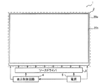
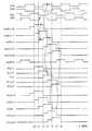
図1は、本実施形態に係る液晶表示装置の概略構成を示した模式図である。液晶表示装置1は、表示パネル2、ソースドライバ3、表示制御回路4、及び電源5を有する。表示パネル2は、アクティブマトリクス基板20aと、対向基板20bと、これら基板に挟持された液晶層(図示略)とを有する。図1において図示を省略しているが、アクティブマトリクス基板20aと対向基板20bとを挟むように、一対の偏光板が設けられている。対向基板20bには、ブラックマトリクスと、赤(R)、緑(G)、青(B)の3色のカラーフィルタと、共通電極(いずれも図示略)が形成されている。<First Embodiment>
(Configuration of liquid crystal display device)
FIG. 1 is a schematic diagram showing a schematic configuration of the liquid crystal display device according to the present embodiment. The liquid
図1に示すように、アクティブマトリクス基板20aは、フレキシブル基板に形成されたソースドライバ3と電気的に接続されている。表示制御回路4は、表示パネル2、ソースドライバ3、及び電源5と電気的に接続されている。表示制御回路4は、ソースドライバ3と、アクティブマトリクス基板20aに設けられた後述のシフトレジスタ回路(以下、ゲートドライバ)に制御信号を出力する。電源5は、表示パネル2、ソースドライバ3、及び表示制御回路4と電気的に接続されており、各々に電源電圧信号を供給する。 As shown in FIG. 1, the
(アクティブマトリクス基板の構成)
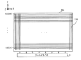
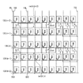
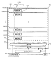
図2は、アクティブマトリクス基板20aの概略構成を示す模式図である。アクティブマトリクス基板20aにおいて、X軸方向の一端から他端までM(M:自然数)本のゲート線13G(1)〜13G(M)が一定の間隔で略平行に形成されている。以下、ゲート線を区別しないときは、ゲート線13Gと称する。アクティブマトリクス基板20aには、各ゲート線13Gと交差するように複数のソース線15Sが形成されている。ゲート線13Gとソース線15Sとで囲まれる領域が1つの画素を形成し、各画素は、カラーフィルタのいずれかの色に対応している。(Configuration of active matrix substrate)
FIG. 2 is a schematic diagram showing a schematic configuration of the
図3は、アクティブマトリクス基板20aと、アクティブマトリクス基板20aと接続されている各部の概略構成を示す模式図である。図3では、便宜上、ソース線15Sの図示を省略している。図3の例に示すように、アクティブマトリクス基板20aには、表示領域201の領域201aと201bの各々に、ゲートドライバ11A、11Bが設けられている。ゲートドライバ11Aは、ゲート線13G(1)、13G(3)、…13G(M)の奇数行のゲート線13Gに対して設けられ、配線15Lを介して接続された複数の駆動回路11を有する。また、ゲートドライバ11Bは、ゲート線13G(2)、13G(4)、…13G(M−1)の偶数行のゲート線13Gに対して設けられ、配線15Lを介して接続された複数の駆動回路11を有する。 FIG. 3 is a schematic diagram showing a schematic configuration of each part connected to the
図3に示すアクティブマトリクス基板20aにおいて、ソースドライバ3が設けられている辺の額縁領域202には、端子部12gが設けられている。端子部12gは、表示制御回路4及び電源5と接続されている。端子部12gは、表示制御回路4及び電源5から出力される制御信号や電源電圧信号等の信号を受け取る。端子部12gに入力された制御信号及び電源電圧信号等の信号は、配線15Lを介して各駆動回路11に供給される。駆動回路11は、供給される信号に応じて、接続されているゲート線13Gに対し、選択状態と非選択状態の一方を示す電圧信号を出力する。以下の説明において、ゲート線13Gが選択されている状態をゲート線13Gの駆動と呼ぶ。 In the
また、アクティブマトリクス基板20aにおける額縁領域202には、ソースドライバ3とソース線15S(図2参照)とを接続する端子部12sが設けられている。ソースドライバ3は、表示制御回路4から入力される制御信号に応じて、各ソース線15S(図2参照)にデータ信号を出力する。 Further, the
表示制御回路4は、制御信号として、2水平期間ごとに、電位がHレベル(VDD)とLレベル(VSS)とを繰り返す信号(以下、クロック信号)と、クロック信号のHレベルと同じ電位の信号(以下、リセット信号)とを端子部12gへ供給する。 The
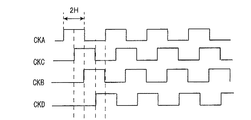
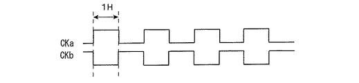
図4は、クロック信号の波形を例示した図である。本実施形態では、クロック信号として、位相が1/4周期ずつずれた4相のクロック信号CKA、CKC、CKB、及びCKDが端子部12gへ供給される。なお、この例において、4相のクロック信号を用いるが、例えば、1水平走査期間毎にHレベル(VDD)とLレベル(VSS)とを繰り返し、位相が1/2周期ずれた2相のクロック信号等、位相が異なる複数のクロック信号を用いてもよい。 FIG. 4 is a diagram illustrating the waveform of the clock signal. In the present embodiment, four-phase clock signals CKA, CKC, CKB, and CKD, whose phases are shifted by ¼ period, are supplied to the
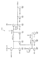
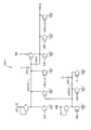
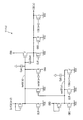
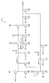
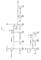
(回路構成)
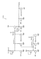
次に、本実施形態における駆動回路11の構成について説明する。図5は、ゲート線13G(n)を駆動する駆動回路11(以下、駆動回路11(n))の等価回路の一例を示す図である。(Circuit configuration)
Next, the configuration of the
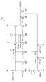
図5に示すように、駆動回路11(n)は、スイッチング素子として、アルファベットA〜Lで示す薄膜トランジスタ(TFT:Thin Film Transistor)(以下、TFT−A〜TFT−L)と、キャパシタCbstとを有する。 As shown in FIG. 5, the drive circuit 11 (n) includes thin film transistors (TFTs) (hereinafter referred to as TFT-A to TFT-L) indicated by alphabets A to L, and a capacitor Cbst as switching elements. Have.
図5において、TFT−Bのソース端子と、TFT−A、TFT−C、及びTFT−Kのドレイン端子と、TFT−Fのゲート端子と、キャパシタCbstの一方の電極とが接続されている内部配線をnetAと称する。また、TFT−Gのソース端子と、TFT−H、TFT−I、及びTFT−Jのドレイン端子と、TFT−Cのゲート端子とが接続されている内部配線をnetBと称する。 In FIG. 5, the source terminal of TFT-B, the drain terminals of TFT-A, TFT-C, and TFT-K, the gate terminal of TFT-F, and one electrode of capacitor Cbst are connected. The wiring is referred to as netA. An internal wiring in which the source terminal of TFT-G, the drain terminals of TFT-H, TFT-I, and TFT-J and the gate terminal of TFT-C are connected is referred to as netB.
本実施形態において、駆動回路11は、表示領域内に設けられるため、netAとnetBは、ソース線15S(図2参照)や画素に設けられる他の素子との間で寄生容量Cpa、Cpbを各々有する。 In the present embodiment, since the
TFT−Aのドレイン端子はnetAと接続され、ゲート端子にリセット信号CLRが供給され、ソース端子に電源電圧信号VSSが供給される。TFT−Aは、リセット信号CLRの電位に応じて、netA(n)をLレベル(VSS)に引き下げる。 The drain terminal of the TFT-A is connected to netA, the reset signal CLR is supplied to the gate terminal, and the power supply voltage signal VSS is supplied to the source terminal. The TFT-A lowers netA (n) to L level (VSS) in accordance with the potential of the reset signal CLR.
TFT−Bのゲート端子には、ゲート線13G(n−2)を駆動する駆動回路11(以下、駆動回路11(n−2))におけるnetA(以下、netA(n−2))が接続され、ドレイン端子は、ゲート線13G(n−1)と接続され、ソース端子は、駆動回路11(n)におけるnetA(以下、netA(n))と接続されている。TFT−Bは、セット信号Sとして、ゲート線13G(n−1)の電位を受け取る。なお、ゲート線13G(1)を駆動する駆動回路11におけるTFT−Bは、セット信号Sとして、表示制御回路4から出力されるゲートスタートパルス信号を受け取る。 The gate terminal of the TFT-B is connected to netA (hereinafter referred to as netA (n-2)) in the drive circuit 11 (hereinafter referred to as drive circuit 11 (n-2)) that drives the
つまり、この例において、駆動回路11(n)におけるTFT−Bのゲート端子は、ゲート線13G(n)の駆動タイミングより2水平走査期間前に駆動されるゲート線13G(n−2)に対して設けられた駆動回路11(n−2)のnetA(n−2)の電位が入力される。TFT−Bは、netA(n−2)の電位に応じて、セット信号Sの電位をnetA(n)に出力し、netA(n)を充電(プリチャージ)する。 That is, in this example, the gate terminal of the TFT-B in the driving circuit 11 (n) is connected to the
TFT−Cは、ゲート端子がnetB(n)と接続され、ドレイン端子がnetA(n)と接続され、ソース端子に電源電圧信号VSSが供給される。TFT−Cは、netB(n)の電位に応じて、netA(n)をLレベル(VSS)に引き下げる。 The TFT-C has a gate terminal connected to netB (n), a drain terminal connected to netA (n), and a power supply voltage signal VSS is supplied to the source terminal. The TFT-C pulls down netA (n) to L level (VSS) in accordance with the potential of netB (n).
TFT−Kは、ゲート端子が、ゲート線13G(n+2)と接続され、ドレイン端子はnetA(n)と接続され、ソース端子に電源電圧信号VSSが供給される。TFT−Kは、ゲート線13G(n+2)の電位に応じて、netA(n)をLレベル(VSS)に引き下げる。 The TFT-K has a gate terminal connected to the
TFT−Fは、ゲート端子がnetA(n)と接続され、ソース端子がゲート線13G(n)に接続され、ドレイン端子にクロック信号CKAが供給される。TFT−Fは、netA(n)の電位に応じて、クロック信号CKAの電位をゲート線13G(n)に出力してキャパシタCbstを充電し、ゲート線13G(n)を選択状態に切り替える。なお、TFT−Fは、比較的負荷の重いゲート線を駆動するため、チャネル幅を大きくする必要がある。図5に示す等価回路においては、TFT−Fを1つのTFTで表しているが、TFT−Fは、複数のTFTを接続して構成される。TFT−Fの具体的な構成例は後述する。 The TFT-F has a gate terminal connected to netA (n), a source terminal connected to the
キャパシタCbstは、一方の電極がnetA(n)と接続され、他方の電極がゲート線13G(n)と接続されている。キャパシタCbstは、TFT−Fから出力されるクロック信号CKAの電位に応じて、netA(n)の電位を昇圧する。 The capacitor Cbst has one electrode connected to the netA (n) and the other electrode connected to the
TFT−Eは、ドレイン端子がゲート線13G(n)と接続され、ゲート端子にリセット信号CLRが供給され、ソース端子に電源電圧信号VSSが供給される。TFT−Eは、リセット信号CLRの電位に応じて、ゲート線13G(n)の電位をLレベル(VSS)に引き下げる。 The TFT-E has a drain terminal connected to the
TFT−Dは、ドレイン端子がゲート線13G(n)と接続され、ゲート端子にクロック信号CKBが供給され、ソース端子に電源電圧信号VSSが供給される。TFT−Dは、クロック信号CKBの電位に応じて、ゲート線13G(n)の電位をLレベル(VSS)に引き下げる。 In the TFT-D, the drain terminal is connected to the
TFT−Lは、ドレイン端子がゲート線13G(n)と接続され、ゲート端子がゲート線13G(n+2)と接続され、ソース端子に電源電圧信号VSSが供給される。TFT−Lは、ゲート線13G(n+2)の電位に応じて、ゲート線13G(n)の電位をLレベル(VSS)に引き下げる。 The TFT-L has a drain terminal connected to the
TFT−Gは、ゲート端子とドレイン端子とが接続され、ゲート端子とドレイン端子にクロック信号CKDが供給され、ソース端子がnetB(n)に接続されている。TFT−Gは、クロック信号CKDの電位に応じて、netB(n)に、(クロック信号CKDのHレベルの電位−閾値電圧)の電位を出力する。 In the TFT-G, a gate terminal and a drain terminal are connected, a clock signal CKD is supplied to the gate terminal and the drain terminal, and a source terminal is connected to netB (n). The TFT-G outputs a potential of (H level potential of the clock signal CKD−threshold voltage) to the netB (n) in accordance with the potential of the clock signal CKD.
TFT−Hは、ドレイン端子がnetB(n)に接続され、ゲート端子にクロック信号CKCが供給され、ソース端子に電源電圧信号VSSが供給される。TFT−Hは、クロック信号CKCの電位に応じて、netB(n)をLレベル(VSS)の電位に引き下げる。 The TFT-H has a drain terminal connected to netB (n), a gate terminal supplied with a clock signal CKC, and a source terminal supplied with a power supply voltage signal VSS. The TFT-H lowers netB (n) to the L level (VSS) potential in accordance with the potential of the clock signal CKC.
TFT−Iは、ドレイン端子がnetB(n)と接続され、ゲート端子にリセット信号CLRが供給され、ソース端子に電源電圧信号VSSが供給される。TFT−Iは、リセット信号CLRの電位に応じて、netB(n)をLレベル(VSS)の電位に引き下げる。 The TFT-I has a drain terminal connected to netB (n), a gate terminal supplied with a reset signal CLR, and a source terminal supplied with a power supply voltage signal VSS. The TFT-I lowers netB (n) to the L level (VSS) potential in accordance with the potential of the reset signal CLR.
TFT−Jは、ドレイン端子がnetB(n)と接続され、ゲート端子がゲート線13G(n―1)と接続され、ソース端子に電源電圧信号VSSが供給される。TFT−Jは、セット信号Sとして、ゲート線13G(n−1)の電位を受け取る。なお、ゲート線13G(1)を駆動する駆動回路11におけるTFT−Jは、セット信号Sとして、表示制御回路4から出力されるゲートスタートパルス信号を受け取る。TFT−Jは、セット信号Sの電位に応じて、netB(n)をLレベル(VSS)の電位に引き下げる。 In the TFT-J, the drain terminal is connected to netB (n), the gate terminal is connected to the
つまり、本実施形態において、TFT−Fは、ゲート線13G(n)に、選択状態に対応する選択電圧を出力する出力部として機能する。TFT−Bは、TFT−Fを動作させるための制御電圧をnetA(n)に出力し、netA(n)を充電するプリチャージ部として機能する。TFT−FとキャパシタCbstは、netA(n)の電位を昇圧することにより、TFT-Fのゲート電圧を昇圧する昇圧部として機能する。また、TFT−A、TFT−K、及びTFT−Cは、netA(n)の電位を引き下げるゲート電圧放電部として機能する。TFT−E、TFT−D、及びTFT−Lは、ゲート線13Gに非選択電圧を出力するゲート線放電部として機能する。 That is, in the present embodiment, the TFT-F functions as an output unit that outputs a selection voltage corresponding to the selected state to the
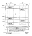
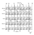
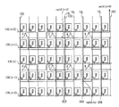
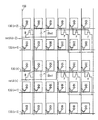
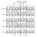
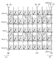
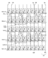
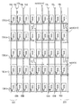
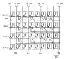
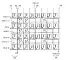
(配置例)
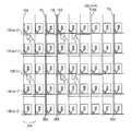
次に、本実施形態における駆動回路11の配置例について説明する。図6A〜図6Dは、駆動回路11(n)及び駆動回路11(n+2)の配置例を示す模式図である。なお、図6A〜図6Dでは、便宜上、アルファベットA〜Lのみ記載し、”TFT−”の表記を省略しているが、A〜Lは、図5に示したTFT−A〜TFT−Lに対応している。また、図6A〜6Dに示す各表示領域は、列201〜204において連続しているものとする。(Arrangement example)
Next, an arrangement example of the
図6A〜6Dに示すように、駆動回路11(n)を構成する各素子は、ゲート線13G(n−2)〜13G(n)の各ゲート線の間に配置されている。また、駆動回路11(n+2)を構成する各素子は、ゲート線13G(n)〜13G(n+2)の各ゲート線の間に配置されている。駆動回路11(n)は、ゲート線13G(n−1)、ゲート線13G(n)、及びゲート線13G(n+2)と接続され、駆動回路11(n+2)は、ゲート線13G(n+1)、ゲート線13G(n+2)、及び図示しないゲート線13G(n+4)と接続されている。 As shown in FIGS. 6A to 6D, each element constituting the drive circuit 11 (n) is arranged between the
図6A、6B、及び6Dに示すように、駆動回路11(n)と駆動回路11(n+2)のTFT−E、TFT−I、TFT−H、TFT−G、TFT−J、TFT−C、TFT−A、TFT−K、TFT−D、TFT−Lは、電源電圧信号VSSを供給する配線15Lを介して接続されている。また、図6Aに示すように、これら駆動回路11のTFT−H、TFT−Gは、クロック信号CKC、及びCKDを各々供給する配線15Lを介して接続されている。 As shown in FIGS. 6A, 6B, and 6D, TFT-E, TFT-I, TFT-H, TFT-G, TFT-J, and TFT-C of the drive circuit 11 (n) and the drive circuit 11 (n + 2) The TFT-A, TFT-K, TFT-D, and TFT-L are connected via a
配線15Lは、アクティブマトリクス基板20aにおけるソース線15Sが形成されたソース層において、ソース線15Sと略平行に設けられる。また、駆動回路11におけるnetAの配線は、ゲート線13Gが形成されたゲート層において、ゲート線13Gと略平行に設けられる。 The
図6A及び図6Bに示すように、電源電圧信号VSSを供給する配線15Lは、TFT−E、TFT−I、TFT−H、TFT−G、TFT−J、TFT−C、TFT−A、TFT−Kが配置された列とは異なる他の列において、端子部12g(図3参照)からソース線15Sと略平行となるように配線され、これらTFTが配置された画素まで引き回されている。また、図6Dにおいても、電源電圧信号VSSを供給する配線15Lは、TFT−D、TFT−Lが配置された列とは異なる他の列において、端子部12g(図3参照)からソース線15Sと略平行となるように配線され、これらTFTが配置された画素まで引き回されている。 As shown in FIGS. 6A and 6B, the
また、図6Aにおいて、駆動回路11(n)におけるTFT−Hのゲート端子はクロック信号CKCを供給する配線15Lに接続され、駆動回路11(n+2)におけるTFT−Hのゲート端子は、クロック信号CKDを供給する配線15Lに接続されている。また、駆動回路11(n)におけるTFT−Gのゲート端子はクロック信号CKDを供給する配線15Lに接続され、駆動回路11(n+2)におけるTFT−Gのゲート端子は、クロック信号CKCを供給する配線15Lに接続されている。 In FIG. 6A, the gate terminal of the TFT-H in the driving circuit 11 (n) is connected to the
また、図6Cに示すように、TFT−Fは、3つのTFTが並列に接続されて構成されている。接続されるTFTの数はこれに限らず、1つ以上のTFTが接続されていればよい。また、TFT−F以外の他のTFT及びキャパシタCbstについても、必要に応じて複数のTFT及びキャパシタを並列に接続して構成してもよい。 Further, as shown in FIG. 6C, the TFT-F is configured by connecting three TFTs in parallel. The number of TFTs to be connected is not limited to this, and one or more TFTs may be connected. Also, other TFTs and capacitors Cbst other than TFT-F may be configured by connecting a plurality of TFTs and capacitors in parallel as necessary.
図6Cにおいて、駆動回路11(n)における3つのTFT−Fの各ドレイン端子は、クロック信号CKAが供給される配線15Lに接続されている。一方、駆動回路11(n+2)における3つのTFTの各ドレイン端子は、クロック信号CKBが供給される配線15Lに接続されている。また、各TFT−Fにクロック信号CKA、CKBを供給する配線15Lは、TFT−Fが配置された列と異なる列において、端子部12g(図3参照)からソース線15Sと略平行となるように配線され、各TFT−Fが配置された画素まで引き回されている。 In FIG. 6C, the drain terminals of the three TFT-Fs in the driving circuit 11 (n) are connected to the
このように、ゲートドライバ11A、11Bにおける各駆動回路11は、ゲートドライバにおいて隣接する駆動回路11に供給されるクロック信号と逆位相のクロック信号が供給される。また、隣接するゲート線13Gを駆動する駆動回路11に供給されるクロック信号は互いに位相が1/4周期ずれている。例えば、駆動回路11(n)におけるTFT−Fのドレイン端子にクロック信号CKAが入力される場合、駆動回路11(n−2)及び駆動回路11(n+2)におけるTFT−Fのドレイン端子にはクロック信号CKBが入力される。また、駆動回路11(n−1)におけるTFT−Fのドレイン端子にはクロック信号CKD、駆動回路11(n+1)におけるTFT−Fのドレイン端子には、クロック信号CKCが入力される。 In this manner, each
(動作例)
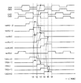
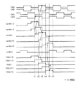
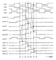
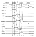
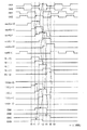
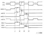
次に、駆動回路11の動作について説明する。図7は、駆動回路11(n)がゲート線13G(n)を駆動する際のタイミングチャートである。(Operation example)
Next, the operation of the
駆動回路11(n)には、表示制御回路4から供給されるクロック信号CKA、CKB、CKC、及びCKDが入力される。なお、図7では図示を省略しているが、1垂直走査期間毎に一定期間H(High)レベルとなるリセット信号CLRが表示制御回路4から各駆動回路11に入力される。リセット信号CLRが入力されると、駆動回路11(n)におけるnetA(n)、netB(n)、及びゲート線13Gの電位はL(Low)レベルに遷移する。 Clock signals CKA, CKB, CKC, and CKD supplied from the
時刻t1のタイミングで、ゲート線13G(n−1)が選択状態に切り替えられ、駆動回路11(n)のTFT−Bのドレイン端子に、セット信号Sとして、ゲート線13G(n−1)のHレベルの電位が入力される。TFT−Bのゲート端子には、netA(n−2)の電位が入力される。netA(n−2)の電位は、時刻t1より前にHレベルとなっており、TFT−Bは、時刻t1においてオン状態となっている。TFT−Bは、netA(n−2)の電位がLレベルに遷移する時刻t2までオン状態となり、時刻t1からt2の間、netA(n)は、ゲート線13G(n−1)のHレベルの電位(VDD)にプリチャージされる。 At time t1, the
TFT−Fのゲート端子には、netA(n)のHレベルの電位が入力され、オン状態となる。時刻t1において、TFT−Dのゲート端子にはクロック信号CKBのHレベルの電位が入力されるため、TFT−Dはオン状態となり、ゲート線13G(n)にLレベルの電位(VSS)が入力される。 The gate terminal of the TFT-F is inputted with the H level potential of netA (n) and is turned on. At time t1, since the H-level potential of the clock signal CKB is input to the gate terminal of the TFT-D, the TFT-D is turned on, and the L-level potential (VSS) is input to the
また、時刻t1において、クロック信号CKDの電位はHレベルであり、クロック信号CKCの電位はLレベルである。これにより、TFT−Gはオン状態、TFT−Hはオフ状態となる。TFT−Jのゲート端子には、セット信号Sとして、ゲート線13G(n−1)のHレベルの電位が入力され、TFT−Jはオン状態になる。そのため、netB(n)はLレベルの電位に維持され、TFT−Cはオフ状態となる。 At time t1, the potential of the clock signal CKD is at the H level, and the potential of the clock signal CKC is at the L level. As a result, the TFT-G is turned on and the TFT-H is turned off. The H-level potential of the
時刻t2において、クロック信号CKAの電位がHレベルとなり、TFT−Fを介してクロック信号CKAのHレベルの電位がゲート線13G(n)に入力される。ゲート線13G(n)の電位の上昇に伴って、netA(n)とゲート線13G(n)の間に接続されたキャパシタCbstにより、netA(n)は、クロック信号CKAのHレベルの電位よりも高い電位まで充電される。つまり、netA(n)は、(プリチャージ電圧VDD+TFT−Fの閾値電圧Vth)よりも高い電位に充電される。 At time t2, the potential of the clock signal CKA becomes H level, and the H level potential of the clock signal CKA is input to the
時刻t2において、ゲート線13G(n−1)の電位はHレベルであり、TFT−Jはオン状態を維持する。時刻t3において、クロック信号CKCの電位がHレベルに遷移し、TFT−Hがオン状態となる。そのため、時刻t2からt4の間、netB(n)はLレベルの電位に維持される。 At time t2, the potential of the
また、時刻t2において、クロック信号CKBの電位がHレベルからLレベルに遷移し、TFT−Dはオフ状態となる。これにより、時刻t2からt4において、ゲート線13G(n)に、クロック信号CKAのHレベルの電位(選択電圧)が出力されてゲート線13G(n)が選択状態に切り替えられる。 At time t2, the potential of the clock signal CKB transits from the H level to the L level, and the TFT-D is turned off. Thereby, from time t2 to t4, the H-level potential (selection voltage) of the clock signal CKA is output to the
なお、ゲート線13G(n+1)を駆動する駆動回路11(n+1)は、ゲート線13G(n)をセット信号Sとして、駆動回路11(n)と同様に動作し、ゲート線13G(n+1)は、時刻t3のタイミングで選択状態に切り替えられる。また、ゲート線13G(n+2)を駆動する駆動回路11(n+2)は、ゲート線13G(n+1)をセット信号Sとして、駆動回路11(n)と同様に動作し、ゲート線13G(n+2)は、時刻t4のタイミングで選択状態に切り替えられる。 Note that the drive circuit 11 (n + 1) that drives the
時刻t4において、クロック信号CKBの電位がHレベルに遷移し、TFT−Dはオン状態となる。また、時刻t4において、ゲート線13G(n+2)の電位がHレベルに遷移するため、TFT-KとTFT-Lもオン状態となる。これにより、TFT−D及びTFT−Lを介してゲート線13G(n)にLレベルの電位が入力され、ゲート線13G(n)は非選択状態に切り替えられる。また、TFT−Kを介してnetA(n)にはLレベルの電位が入力される。このとき、クロック信号CKCの電位はHレベルであり、TFT−Hはオン状態を維持するため、netB(n)の電位はLレベルに維持される。 At time t4, the potential of the clock signal CKB changes to the H level, and the TFT-D is turned on. At time t4, since the potential of the
続いて、時刻t5において、クロック信号CKDの電位がHレベル、クロック信号CKCの電位がLレベルに遷移すると、TFT−Hはオフ状態、TFT−Gはオン状態となる。これにより、netB(n)は、クロック信号CKDのHレベルの電位よりTFT−Gの閾値電圧分小さい電位に充電される。このとき、TFT−K及びTFT−Lはオン状態となっており、TFT−Cはオン状態となるため、netA(n)とゲート線13G(n)はLレベルの電位に維持される。 Subsequently, at time t5, when the potential of the clock signal CKD transitions to the H level and the potential of the clock signal CKC transitions to the L level, the TFT-H is turned off and the TFT-G is turned on. Thereby, netB (n) is charged to a potential that is smaller than the H-level potential of the clock signal CKD by the threshold voltage of the TFT-G. At this time, since the TFT-K and the TFT-L are in an on state and the TFT-C is in an on state, the netA (n) and the
時刻t6以降は、クロック信号CKBがHレベルの電位となるタイミングで、ゲート線13G(n)は、TFT−Dを介してLレベルの電位に維持される。 After time t6, the
また、時刻t6以降は、クロック信号CKDがHレベルの電位となるタイミングで、netB(n)の電位がHレベルに充電され、netA(n)は、TFT−Cを介してLレベルの電位に維持される。 Further, after time t6, at the timing when the clock signal CKD becomes the H level potential, the potential of netB (n) is charged to the H level, and netA (n) becomes the potential of the L level via the TFT-C. Maintained.
つまり、netB(n)は、TFT−Cを介してnetA(n)の電位をLレベルに維持するためのものである。ただし、ゲート線13G(n)を選択状態に切り替える際、TFT−Cはオフ状態である必要がある。そのため、ゲート線13G(n)の非選択期間に、クロック信号CKDの電位に応じてTFT−Cがオン状態となるように、駆動回路11(n)は構成されている。また、TFT−Fは、クロック信号CKAを供給する配線15Lとの間で寄生容量を持つ。そのため、netA(n)をLレベルの電位に保持する期間に、その寄生容量を介してnetA(n)にクロック信号CKAに同期したノイズが入る。このノイズを回避するため、クロック信号CKAの電位がHレベルとなるタイミングでTFT−Cがオン状態となるように、クロック信号CKDと同じタイミングでnetB(n)の電位をHレベルに遷移させている。 That is, netB (n) is for maintaining the potential of netA (n) at the L level via TFT-C. However, when the
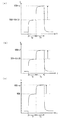
ここで、図8に、ダイオード接続されたTFT−Bを用いた従来の駆動回路100(n)の等価回路を示す。図8に示す駆動回路100(n)は、TFT−Bのゲート端子及びドレイン端子に、ゲート線13G(n−2)の電位を入力する点を除き、駆動回路11(n)と同じ構成である。 Here, FIG. 8 shows an equivalent circuit of a conventional driving circuit 100 (n) using a diode-connected TFT-B. The drive circuit 100 (n) shown in FIG. 8 has the same configuration as the drive circuit 11 (n) except that the potential of the
図9の(a)は、表示領域の外側に駆動回路100(n)を配置した場合の、netA(n)のプリチャージ期間Tpと、ゲート線13G(n)の選択期間TsにおけるnetA(n)の電位変化を表した図である。また、図9の(b)は、表示領域内に駆動回路100(n)を配置した場合の、netA(n)のプリチャージ期間Tpと、ゲート線13G(n)の選択期間TsにおけるnetA(n)の電位変化を表した図である。 FIG. 9A shows the netA (n) in the precharge period Tp of netA (n) and the selection period Ts of the
図9の(a)に示すように、表示領域外に設けられた駆動回路100(n)では、プリチャージ期間Tpにおいて、ゲート線13G(n−2)のHレベルの電位(VDD)よりTFT−Bの閾値電圧(Vth(B))分だけ小さい電位(VDD−Vth(B))が、netA(n)にプリチャージされる。選択期間Tsでは、TFT−Fを介してクロック信号CKAのHレベルの電位がゲート線13G(n)に入力され、キャパシタCbstによって、netA(n)の電位は、プリチャージ電圧よりも高い電位(VDD+α)まで突き上げられる。 As shown in FIG. 9A, in the driving circuit 100 (n) provided outside the display region, the TFT is applied from the H level potential (VDD) of the
一方、表示領域内に駆動回路100(n)を設ける場合、駆動回路100(n)は、表示領域に設けられたソース線15S等の他の素子との間に寄生容量を持ち、netA(n)の寄生容量は、表示領域外に設ける場合よりも大きくなる。その結果、キャパシタCbstを介したnetA(n)の電位の上昇効率が低下し、図9の(b)に示すように、選択期間TsにおけるnetA(n)の電位(VDD+β(β<α))は、表示領域の外側に駆動回路100(n)を配置する場合よりも小さくなる。これにより、TFT−Fのゲート電圧が低下し、駆動回路を安定して動作させることができず、ゲートドライバの動作マージンが低下する。 On the other hand, when the driver circuit 100 (n) is provided in the display region, the driver circuit 100 (n) has a parasitic capacitance with another element such as the
これに対し、上述した第1実施形態では、TFT−Bのゲート端子にnetA(n−2)の電位を入力し、ドレイン端子にゲート線13G(n−1)の電位をセット信号として入力する。これにより、図9の(c)に示すように、プリチャージ期間TpにおけるnetA(n)のプリチャージ電圧は、TFT−Bの閾値電圧分だけ低下することなく、ゲート線13G(n)のHレベルの電位(VDD)となる。これにより、表示領域内に設けた駆動回路11(n)のnetA(n)の寄生容量の影響によってnetA(n)の電位の上昇効率が低下しても、選択期間TsにおけるnetA(n)の電位を図9の(a)と同等以上まで引き上げることができ、駆動回路を安定して動作させ、ゲートドライバの動作マージンを向上させることができる。 In contrast, in the first embodiment described above, the potential of netA (n-2) is input to the gate terminal of the TFT-B, and the potential of the
<第1実施形態の応用例>
上述した第1実施形態では、駆動回路11(n)のTFT−Bに入力されるセット信号Sとしてゲート線13G(n−1)の電位を入力する例について説明した。本応用例では、TFT−Bに入力されるセット信号Sとしてクロック信号を入力する例について説明する。以下の説明において、第1実施形態と異なる構成について説明する。<Application example of the first embodiment>
In the first embodiment described above, the example in which the potential of the
(回路構成)
図10は、本応用例における駆動回路110の等価回路を例示した図である。図10に示すように、ゲート線13G(n)を駆動する駆動回路110(n)は、TFT−Bのドレイン端子に、クロック信号CKDが入力される点を除き、駆動回路11(n)と同じ構成を有する。(Circuit configuration)
FIG. 10 is a diagram illustrating an equivalent circuit of the
(配置例)
図11は、表示領域における駆動回路110(n)と、ゲート線13G(n+2)を駆動する駆動回路110(n+2)のTFT−Bの接続例を示す模式図である。なお、図11では、便宜上、”TFT−”の表記を省略しているが、図11においてアルファベットで示すTFTは、図10における同じアルファベットが付されたTFTと対応している。図11に示すように、駆動回路110(n)におけるTFT−Bのドレイン端子は、クロック信号CKDが供給される配線15Lに接続されている。また、駆動回路110(n+2)におけるTFT−Bのドレイン端子は、クロック信号CKDと逆位相のクロック信号CKCが供給される配線15Lに接続されている。(Arrangement example)
FIG. 11 is a schematic diagram showing a connection example of the TFT-B of the driving circuit 110 (n) in the display region and the driving circuit 110 (n + 2) that drives the
(動作例)
図12は、駆動回路110(n)がゲート線13G(n)を駆動する際のタイミングチャートである。以下、第1実施形態と異なる動作について説明する。(Operation example)
FIG. 12 is a timing chart when the driving circuit 110 (n) drives the
時刻t1において、クロック信号CKDの電位はHレベルとなり、このときTFT−Bはオン状態となっているため、TFT−Bを介してnetA(n)にクロック信号CKDのHレベル(VDD)の電位がプリチャージされる。なお、クロック信号CKDは、2水平走査期間ごとにHレベルに遷移するが、TFT−Bは、netA(n−2)の電位がHレベルとなっている期間以外はオフ状態となるため、時刻t2以降は、TFT−Bを介して、クロック信号CKDのHレベルの電位がnetA(n)に入力されない。 At time t1, the potential of the clock signal CKD becomes H level, and at this time, the TFT-B is in an on state. Therefore, the potential of the H level (VDD) of the clock signal CKD is transferred to the netA (n) via the TFT-B. Is precharged. Note that the clock signal CKD changes to the H level every two horizontal scanning periods, but the TFT-B is in the off state except during the period in which the potential of the netA (n-2) is at the H level. After t2, the H level potential of the clock signal CKD is not input to the netA (n) via the TFT-B.
ゲート線13Gは、寄生容量が比較的大きく、ゲート線13Gの出力波形は鈍りやすい。そのため、第1実施形態のように、TFT−Bのドレイン端子に、ゲート線13G(n−1)の電位を入力すると、ゲート線13G(n−1)の出力波形の鈍りの影響を受け、TFT−Bを介してnetA(n)をプリチャージする能力が低下する。また、駆動回路110における各TFTの劣化に伴って、ゲート線13Gの出力波形の鈍りは次第に大きくなる。その結果、netA(n)をプリチャージする能力がより低下し、駆動回路の動作が不安定になる。第1実施形態の応用例では、TFT−Bのドレイン端子にクロック信号を入力するため、ゲート線13Gの出力波形の鈍りの程度に関係なく、netAを適切にプリチャージすることができる。 The
<第2実施形態>
上述の第1実施形態とその応用例では、netAのプリチャージ電圧の低下を抑制し、ゲートドライバの動作マージンを向上させる例を説明した。ゲートドライバの動作マージンの低下の要因として、ゲート線を非選択期間に切り替える際のnetAの電位の引き下げが不十分であることが挙げられる。特に、表示領域内にゲートドライバを配置する場合には、表示領域内に配置されたソース線15Sや配線15L等の素子との間に生じる寄生容量の影響を受け、netAを確実にLレベルに引き下げることができないことがある。本実施形態では、ゲートドライバの動作マージンを向上させるべく、ゲート線を非選択状態に遷移させる際にnetAの電位の引き下げをより確実に行う例を説明する。以下、第1実施形態と異なる構成について説明する。Second Embodiment
In the first embodiment and its application example, the example in which the decrease in the precharge voltage of netA is suppressed and the operation margin of the gate driver is improved has been described. As a cause of a decrease in the operation margin of the gate driver, there is an insufficient reduction in the potential of netA when the gate line is switched to the non-selection period. In particular, when a gate driver is arranged in the display area, netA is reliably set to L level due to the influence of parasitic capacitance generated between elements such as the
(回路構成)
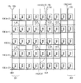
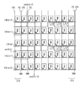
図13は、本実施形態における駆動回路111の等価回路を示す図である。図13に示すように、ゲート線13G(n)を駆動する駆動回路111(n)は、netA(n)のプリチャージ用のTFT−Bは、ダイオード接続されている。TFT−Bのゲート端子とドレイン端子には、ゲート線13G(n−2)の電位が入力される。また、TFT−Kのゲート端子には、ゲート線13G(n+2)を駆動する駆動回路111(n+2)におけるnetA(n+2)の電位が入力され、ドレイン端子には、クロック信号CKAの電位が入力される。(Circuit configuration)
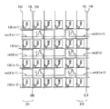
FIG. 13 is a diagram showing an equivalent circuit of the
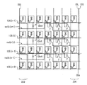
(配置例)
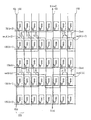
図14A及び14Bは、表示領域における駆動回路111(n)と、駆動回路111(n+2)のTFT−K、及びTFT−Bの接続例を示す模式図である。なお、図14及び14Bでは、便宜上、”TFT−”の表記を省略しているが、図14A及び14Bにおいてアルファベットで示すTFTは、図13における同じアルファベットが付されたTFTと対応している。(Arrangement example)
14A and 14B are schematic diagrams illustrating a connection example of the driver circuit 111 (n) and the TFT-K and TFT-B of the driver circuit 111 (n + 2) in the display region. 14 and 14B, the notation of “TFT−” is omitted for convenience, but the TFTs indicated by alphabets in FIGS. 14A and 14B correspond to the TFTs denoted by the same alphabets in FIG.
図14Aに示すように、駆動回路111(n)におけるTFT−Kのゲート端子は、netA(n+2)に接続され、駆動回路111(n+2)におけるTFT−Kのゲート端子は、netA(n+4)に接続されている。駆動回路111(n)におけるTFT−Kのドレイン端子は、クロック信号CKAを供給する配線15Lに接続され、駆動回路111(n+2)におけるTFT−Kのドレイン端子は、クロック信号CKBを供給する配線15Lに接続されている。 As shown in FIG. 14A, the gate terminal of the TFT-K in the drive circuit 111 (n) is connected to netA (n + 2), and the gate terminal of the TFT-K in the drive circuit 111 (n + 2) is connected to netA (n + 4). It is connected. The drain terminal of the TFT-K in the driving circuit 111 (n) is connected to the
また、図14Bに示すように、駆動回路111(n)におけるTFT−Bのゲート端子とドレイン端子は、ゲート線13G(n−2)に接続され、駆動回路111(n+2)におけるTFT−Bのゲート端子とドレイン端子は、ゲート線13G(n)に接続されている。 As shown in FIG. 14B, the gate terminal and the drain terminal of the TFT-B in the driving circuit 111 (n) are connected to the
(動作例)
図15は、駆動回路111(n)がゲート線13G(n)を駆動する際のタイミングチャートである。以下、第1実施形態と異なる動作について説明する。(Operation example)
FIG. 15 is a timing chart when the drive circuit 111 (n) drives the
図15に示す時刻t0からt2において、ゲート線13G(n−2)が選択状態となり、駆動回路111(n)におけるTFT−Bのゲート端子とドレイン端子に、ゲート線13G(n−2)のHレベルの電位が入力される。これにより、TFT−Bがオン状態となり、netA(n)に、TFT−Bを介して、ゲート線13G(n−2)のHレベルの電位よりTFT−Bの閾値電圧だけ小さい電位がプリチャージされる。 From time t0 to t2 shown in FIG. 15, the
図15に示す時刻t2からt4において、クロック信号CKAのHレベルの電位がTFT−Fを介してゲート線13G(n)に入力される。netA(n)の電位は、キャパシタCbstを介してクロック信号CKAのHレベルよりも高い電位まで突き上げられ、このnetA(n)の電位がTFT−Fのゲート端子に入力され、ゲート線13G(n)にクロック信号CKAのHレベルの電位が入力されて選択状態となる。 From time t2 to time t4 shown in FIG. 15, the H level potential of the clock signal CKA is input to the
駆動回路111(n)におけるTFT−Jは、ゲート線13G(n−1)の電位がHレベルとなる時刻t1から時刻t3の期間にオン状態となり、TFT−Hは、クロック信号CKCの電位がHレベルとなる時刻t3から時刻t5の期間にオン状態となる。これにより、時刻t1から時刻t5において、netB(n)は、Lレベルの電位に維持される。 The TFT-J in the driver circuit 111 (n) is turned on during a period from time t1 to time t3 when the potential of the
図15に示すように、netA(n+1)は、時刻t1にプリチャージが開始され、時刻t3に、ゲート線13G(n+1)は選択状態に切り替えられる。また、netA(n+2)は、時刻t2でプリチャージが開始され、時刻t4に、ゲート線13G(n+2)は選択状態に切り替えられる。 As shown in FIG. 15, precharge of netA (n + 1) is started at time t1, and the
時刻t4において、netA(n+2)の電位がHレベルに遷移すると、TFT−Kがオン状態となる。このとき、クロック信号CKAの電位はLレベルであるため、netA(n)の電位は、TFT−Kを介してHレベル(VDD)からLレベル(VSS)に引き下げられる。また、TFT−Lのゲート端子にゲート線13G(n+2)のHレベルの電位が入力され、TFT−Lがオン状態となるため、ゲート線13G(n)はHレベル(VDD)からLレベル(VSS)の電位に遷移する。 When the potential of netA (n + 2) transitions to the H level at time t4, the TFT-K is turned on. At this time, since the potential of the clock signal CKA is at the L level, the potential of netA (n) is lowered from the H level (VDD) to the L level (VSS) via the TFT-K. Further, since the H-level potential of the
時刻t6以降は、netA(n+2)の電位がLレベルとなるため、TFT−Kはオフ状態となるが、クロック信号CKDの電位がHレベルとなるタイミングで、netB(n)の電位がHレベルとなり、netA(n)は、TFT−Cを介してLレベルの電位に維持される。 After time t6, the potential of netA (n + 2) becomes L level, so that the TFT-K is turned off, but the potential of netB (n) becomes H level at the timing when the potential of the clock signal CKD becomes H level. Thus, netA (n) is maintained at the L level potential via the TFT-C.
上述した第2実施形態では、netA(n)をLレベルに引き下げるTFT−Kのゲート端子に、netA(n+2)が接続される。駆動回路111におけるnetAは、ゲート線13Gの選択期間において、キャパシタCbstを介して選択電圧よりも高い電位まで突き上げられる。そのため、TFT−Kのゲート電圧が向上し、TFT−Kのドレイン端子からソース端子へと流れる電流値が大きくなり、TFT−Kの駆動力が向上する。その結果、表示領域内に駆動回路111を配置することにより、netAに寄生容量Cpaが生じても、ゲート線13Gの非選択期間の遷移時に、TFT−Kを介してnetAの電位を十分引き下げることができ、駆動回路111を安定して動作させることができる。 In the second embodiment described above, netA (n + 2) is connected to the gate terminal of the TFT-K that pulls netA (n) to the L level. The netA in the
<第3実施形態>
上述した第2実施形態では、ゲートドライバの動作マージンを向上させるべく、ゲート電圧放電部として機能するTFT−Kのゲート端子に、他の駆動回路のnetAを接続し、TFT−Kの駆動力を向上させる例を説明した。本実施形態では、ゲート線の非選択期間の遷移時におけるゲート線の放電を強化し、ゲートドライバの動作マージンの向上を図る。以下、第2実施形態と異なる構成について説明する。<Third Embodiment>
In the second embodiment described above, in order to improve the operation margin of the gate driver, the gate A of the TFT-K functioning as a gate voltage discharging unit is connected to the netA of another driving circuit, and the driving power of the TFT-K is increased. The example which improves is demonstrated. In the present embodiment, the gate line discharge is enhanced at the transition of the non-selection period of the gate line, and the operation margin of the gate driver is improved. Hereinafter, a configuration different from the second embodiment will be described.
(回路構成)
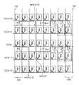
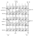
図16は、本実施形態における駆動回路112の等価回路を例示した図である。図16に示すように、ゲート線13G(n)を駆動する駆動回路112(n)において、netA(n)の電位を引き下げるためのTFT−Kは、ゲート端子にゲート線13G(n+2)が接続され、ドレイン端子にnetA(n)が接続され、ソース端子に電源電圧信号VSSが入力されている。また、ゲート線13G(n)に非選択電圧を出力するTFT−Lは、ゲート端子に、駆動回路112(n+2)におけるnetA(n+2)が接続され、ドレイン端子にクロック信号CKAが入力され、ソース端子にゲート線13G(n)が接続されている。(Circuit configuration)
FIG. 16 is a diagram illustrating an equivalent circuit of the
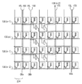
(配置例)
図17A及び17Bは、表示領域における駆動回路112(n)と、駆動回路112(n+2)のTFT−K、及びTFT−Lの接続例を示す模式図である。なお、図17A及び17Bでは、便宜上、”TFT−”の表記を省略しているが、図17A及び17Bにおいてアルファベットで示すTFTは、図16における同じアルファベットが付されたTFTと対応している。(Arrangement example)
17A and 17B are schematic diagrams illustrating a connection example of the driver circuit 112 (n) and the TFT-K and TFT-L of the driver circuit 112 (n + 2) in the display region. 17A and 17B, the notation of “TFT−” is omitted for the sake of convenience, but TFTs indicated by alphabets in FIGS. 17A and 17B correspond to TFTs denoted by the same alphabets in FIG.
図17Aに示すように、駆動回路112(n)におけるTFT−Kのゲート端子は、ゲート線13G(n+2)に接続され、駆動回路112(n+2)におけるTFT−Kのゲート端子は、ゲート線13G(n+4)に接続されている。駆動回路112(n)と駆動回路112(n+2)におけるTFT−Kのソース端子は、電源電圧信号VSSを供給する配線15Lに接続されている。 As shown in FIG. 17A, the gate terminal of the TFT-K in the driving circuit 112 (n) is connected to the
また、図17Bに示すように、駆動回路112(n)におけるTFT−Lのゲート端子は、netA(n+2)に接続され、ドレイン端子は、クロック信号CKAを供給する配線15Lに接続されている。駆動回路112(n+2)におけるTFT−Lのゲート端子は、netA(n+4)に接続され、ドレイン端子は、クロック信号CKBを供給する配線15Lに接続されている。 As shown in FIG. 17B, the gate terminal of the TFT-L in the driver circuit 112 (n) is connected to netA (n + 2), and the drain terminal is connected to the
(動作例)
次に、駆動回路112(n)の動作について説明する。図18は、駆動回路112(n)がゲート線13G(n)を駆動する際のタイミングチャートである。以下、第2実施形態と異なる駆動回路112(n)の動作について、図18及び図16を用いて説明する。(Operation example)
Next, the operation of the drive circuit 112 (n) will be described. FIG. 18 is a timing chart when the drive circuit 112 (n) drives the
図18に示す時刻t4において、netA(n+2)の電位がHレベルに遷移し、ゲート線13G(n+2)が選択状態に遷移すると、TFT−LとTFT−Kがオン状態となる。このとき、クロック信号CKAの電位はLレベルであるため、ゲート線13G(n)は、TFT−Lを介してLレベル(VSS)の電位が印加される。また、netA(n)は、TFT−Kを介してLレベル(VSS)の電位に引き下げられる。 At time t4 shown in FIG. 18, when the potential of netA (n + 2) changes to the H level and the
時刻t6以降は、netA(n+2)の電位がLレベルとなるため、TFT−Lはオフ状態となるが、クロック信号CKBの電位がHレベルとなるタイミングで、TFT−Dがオン状態となり、TFT−Dを介して、ゲート線13G(n)はLレベルの電位に維持される。また、時刻t6以降、ゲート線13G(n+2)の電位はLレベルとなり、TFT−Kはオフ状態となるが、クロック信号CKDの電位がHレベルとなるタイミングで、netB(n)はTFT−Gを介してHレベルの電位が入力される。これにより、TFT−Cがオン状態となり、netA(n)はLレベルの電位に維持される。 After time t6, since the potential of netA (n + 2) becomes L level, the TFT-L is turned off, but at the timing when the potential of the clock signal CKB becomes H level, the TFT-D is turned on, and the TFT
表示領域内に駆動回路112を配置する場合、クロック信号や電源電圧信号を供給するための配線15Lが画素に設けられるため、表示領域外に駆動回路112を配置する場合と比べて、配線15Lとゲート線13Gとの間の寄生容量が増加し、ゲート線13Gを非選択状態に遷移させる際、ゲート線13Gを確実に非選択状態にできない場合がある。上述の第3実施形態では、ゲート線13G(n)に非選択電圧を出力するTFT−Lのゲート端子にnetA(n+2)を接続してTFT−Lのゲート電圧を向上させ、TFT−Lの駆動力を上げることができるので、ゲート線を非選択状態に遷移させる期間に、ゲート線13G(n)をより確実に非選択状態に遷移させることができる。 When the
<第4実施形態>
上述した第1実施形態から第3実施形態では、出力部として機能するTFTのドレイン端子と、ゲート線放電部として機能するTFTのドレイン端子にクロック信号を入力し、クロック信号を用いてゲート線を充電する例を説明した。本実施形態では、Hレベル(VDD)の直流電圧信号を用いて充電する例について説明する。<Fourth embodiment>
In the first to third embodiments described above, a clock signal is input to the drain terminal of the TFT functioning as an output unit and the drain terminal of the TFT functioning as a gate line discharge unit, and the gate line is connected using the clock signal. An example of charging has been described. In the present embodiment, an example in which charging is performed using a DC voltage signal of H level (VDD) will be described.
(回路構成)
図19は、本実施形態における駆動回路113の等価回路を例示した図である。図19に示すように、ゲート線13G(n)を駆動する駆動回路113(n)は、以下の点において、第1実施形態の応用例の駆動回路と異なっている。(Circuit configuration)
FIG. 19 is a diagram illustrating an equivalent circuit of the
駆動回路113(n)は、TFT−P、内部配線netC(n)、TFT−N、及びTFT−Mを備える。 The drive circuit 113 (n) includes a TFT-P, an internal wiring netC (n), a TFT-N, and a TFT-M.
netC(n)は、TFT−Fのソース端子、キャパシタCbst、TFT−Eのドレイン端子、TFT−Dのドレイン端子が接続されており、netC(n)の電位R(n)は、駆動回路113(n−2)のTFT−Lのゲート端子に入力される。 The netC (n) is connected to the source terminal of the TFT-F, the capacitor Cbst, the drain terminal of the TFT-E, and the drain terminal of the TFT-D. The potential R (n) of the netC (n) Input to the gate terminal of the TFT-L of (n-2).
TFT−Fは、netA(n)の電位に応じて、クロック信号CKAの電位をnetC(n)に出力し、キャパシタCbstを充電する。 The TFT-F outputs the potential of the clock signal CKA to netC (n) according to the potential of netA (n) to charge the capacitor Cbst.
TFT−Eは、ゲート端子に入力されるリセット信号CLRの電位に応じて、netC(n)をLレベルの電位に引き下げる。 The TFT-E lowers netC (n) to the L level potential in accordance with the potential of the reset signal CLR input to the gate terminal.
TFT−Dは、ゲート端子に入力されるクロック信号CKBの電位に応じて、netC(n)をLレベルの電位に引き下げる。 The TFT-D lowers netC (n) to the L level potential in accordance with the potential of the clock signal CKB input to the gate terminal.
TFT−Lは、ゲート端子に、ゲート線13G(n+2)を駆動する駆動回路113(n+2)におけるnetCの電位R(n+2)が入力される。TFT−Lは、電位R(n+2)に応じて、ゲート線13G(n)に非選択電圧を印加し、Lレベルの電位に引き下げる。 In the TFT-L, the netC potential R (n + 2) in the driving circuit 113 (n + 2) for driving the
TFT−Nは、ゲート端子にリセット信号CLRが入力され、ドレイン端子にゲート線13G(n)が接続され、ソース端子に電源電圧信号VSSが入力される。TFT−Nは、リセット信号CLRの電位に応じて、ゲート線13G(n)に非選択電圧を印加し、Lレベルの電位に引き下げる。 In the TFT-N, the reset signal CLR is input to the gate terminal, the
TFT−Mは、ゲート端子にnetB(n)が接続され、ドレイン端子にゲート線13G(n)が接続され、ソース端子に電源電圧信号VSSが入力される。TFT−Mは、netB(n)の電位に応じて、ゲート線13G(n)に非選択電圧を印加し、Lレベルの電位に引き下げる。 In the TFT-M, netB (n) is connected to the gate terminal, the
TFT−Pは、ゲート端子がnetA(n)と接続され、ドレイン端子にHレベル(VDD)の直流電圧信号が入力され、ソース端子がゲート線13G(n)に接続されている。TFT−Pは、netA(n)の電位に応じて、ゲート線13G(n)をHレベル(VDD)の電位に充電し、選択状態に切り替える。 The TFT-P has a gate terminal connected to netA (n), a drain terminal to which a DC voltage signal of H level (VDD) is input, and a source terminal that is connected to the
つまり、本実施形態において、TFT−Pは出力部として機能し、TFT−FとキャパシタCbstは昇圧部として機能する。また、TFT−L、TFT−M、TFT−Nは、ゲート線放電部として機能する。 That is, in the present embodiment, the TFT-P functions as an output unit, and the TFT-F and the capacitor Cbst function as a boosting unit. The TFT-L, TFT-M, and TFT-N function as a gate line discharge portion.
(配置例)
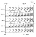
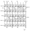
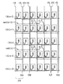
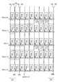
次に、本実施形態における駆動回路の表示領域における配置例について説明する。図20A〜20Fは、表示領域における駆動回路113(n)と駆動回路113(n+2)の配置例を示す模式図である。図20A〜20Fは、列211〜215において連続しているものとする。また、各図では、便宜上、”TFT”の表記を省略しているが、A〜N、Pが付されたTFTは、図19に示すTFT−A〜TFT−N、及びTFT−Pを示している。以下、主に、第1実施形態の応用例と異なる構成の配置について説明する。(Arrangement example)
Next, an arrangement example of the drive circuit in the display area in this embodiment will be described. 20A to 20F are schematic diagrams illustrating an arrangement example of the drive circuit 113 (n) and the drive circuit 113 (n + 2) in the display region. 20A-20F are assumed to be continuous in columns 211-215. In each figure, the notation of “TFT” is omitted for the sake of convenience, but TFTs with A to N and P indicate TFT-A to TFT-N and TFT-P shown in FIG. ing. Hereinafter, an arrangement having a configuration different from the application example of the first embodiment will be mainly described.
図20A〜20Fにおいて、駆動回路113(n)の各素子は、ゲート線13G(n)からゲート線13G(n−2)の間に配置され、駆動回路113(n+2)の各素子は、ゲート線13G(n+2)からゲート線13G(n)の間に配置されている。 20A to 20F, each element of the drive circuit 113 (n) is arranged between the
図20Aに示すように、駆動回路113(n)及び駆動回路113(n+2)の各々におけるTFT−NとTFT−Iは、各ゲート端子に、リセット信号CLRを供給する配線15Lが接続されている。また、図20Bに示すように、駆動回路113(n)におけるTFT−Mのゲート端子は、netB(n)と接続され、駆動回路113(n+2)におけるTFT−Mのゲート端子は、netB(n+2)と接続されている。また、駆動回路113(n)及び駆動回路113(n+2)の各々におけるTFT−Mのソース端子は、図20Aに配置された電源電圧信号VSSを供給する配線15Lに接続されている。 As shown in FIG. 20A, the TFT-N and the TFT-I in each of the drive circuit 113 (n) and the drive circuit 113 (n + 2) are connected to a
本実施形態では、図20Cに示すように、出力部として機能するTFT−Pは、3つのTFT−Pを並列に接続して構成される。図20Cにおいて、Hレベル(VDD)の直流電圧信号を供給する配線15Lは、各TFT−Pが配置された画素まで引き回され、各TFT−Pのドレイン端子と接続されている。 In this embodiment, as shown in FIG. 20C, the TFT-P functioning as an output unit is configured by connecting three TFT-Ps in parallel. In FIG. 20C, a
また、図20Dに示すように、本実施形態では、ゲート線放電部として機能するTFT−Lは、3つのTFT−Lを並列に接続して構成される。図20D及び図20Eに示すように、駆動回路113(n)における各TFT−Lのゲート端子は、駆動回路113(n+2)におけるnetC(n+2)と接続され、netC(n+2)の電位R(n+2)が入力される。また、駆動回路113(n+2)における各TFT−Lのゲート端子は、図示しない駆動回路113(n+4)におけるnetC(n+4)と接続され、netC(n+4)の電位R(n+4)が入力される。また、図20Dに示すように、Lレベル(VSS)の直流電圧信号を供給する配線15Lは、駆動回路113(n)及び駆動回路113(n+2)における各TFT−Lが配置された画素まで引き回され、各TFT−Lのソース端子と接続されている。 As shown in FIG. 20D, in the present embodiment, the TFT-L functioning as the gate line discharge unit is configured by connecting three TFT-Ls in parallel. As shown in FIGS. 20D and 20E, the gate terminal of each TFT-L in the drive circuit 113 (n) is connected to netC (n + 2) in the drive circuit 113 (n + 2), and the potential R (n + 2) of netC (n + 2). ) Is entered. The gate terminal of each TFT-L in the drive circuit 113 (n + 2) is connected to netC (n + 4) in the drive circuit 113 (n + 4) (not shown), and the potential R (n + 4) of netC (n + 4) is input. Further, as shown in FIG. 20D, the
本実施形態では、図20Eに示すように、昇圧部として機能するTFT−Fは1つのTFTで構成される例を説明するが、TFT−Fは、複数のTFTを並列に接続して構成されていてもよい。図20Eにおいて、駆動回路113(n)におけるTFT−Fのソース端子及びキャパシタCbstの一方の電極が接続されたnetC(n)は、図示しない駆動回路113(n−2)におけるTFT−Lのゲート端子に接続され、そのゲート端子に電位R(n)が入力される。また、図20Fに示すように、駆動回路113(n)におけるTFT−E及びTFT−Dのドレイン端子は、キャパシタCbstの一方の電極と接続されたnetC(n)に接続される。駆動回路113(n+2)におけるTFT−E及びTFT−Dのドレイン端子も同様に、キャパシタCbstの一方の電極と接続されたnetC(n+2)に接続される。 In this embodiment, as shown in FIG. 20E, an example in which the TFT-F functioning as the boosting unit is configured by one TFT will be described. The TFT-F is configured by connecting a plurality of TFTs in parallel. It may be. In FIG. 20E, netC (n) to which the source terminal of the TFT-F in the driving circuit 113 (n) and one electrode of the capacitor Cbst are connected is the gate of the TFT-L in the driving circuit 113 (n-2) (not shown). The potential R (n) is input to the gate terminal. As shown in FIG. 20F, the drain terminals of the TFT-E and TFT-D in the driving circuit 113 (n) are connected to netC (n) connected to one electrode of the capacitor Cbst. Similarly, the drain terminals of TFT-E and TFT-D in the drive circuit 113 (n + 2) are also connected to netC (n + 2) connected to one electrode of the capacitor Cbst.
(動作例)
次に、駆動回路113(n)の動作について説明する。図21は、駆動回路113(n)がゲート線13G(n)を駆動する際のタイミングチャートである。以下、第1実施形態の応用例と異なる動作について、図21及び図19を用いて説明する。(Operation example)
Next, the operation of the drive circuit 113 (n) will be described. FIG. 21 is a timing chart when the drive circuit 113 (n) drives the
時刻t1において、クロック信号CKDの電位はHレベルとなり、netA(n−2)の電位はHレベルとなっている。そのため、時刻t1においてTFT−Bはオン状態となっており、TFT−Bを介してnetA(n)にクロック信号CKDのHレベル(VDD)の電位がプリチャージされる。これにより、TFT−Pはオン状態となり、TFT−Pを介して、ゲート線13G(n)は、(VDD−TFT−Pの閾値電圧)の電位に充電される。また、このとき、TFT−Fもオン状態となるが、クロック信号CKAの電位はLレベルであるため、netC(n)の電位R(n)はLレベルに維持される。 At time t1, the potential of the clock signal CKD is at H level, and the potential of netA (n-2) is at H level. Therefore, the TFT-B is in an on state at time t1, and the potential of the H level (VDD) of the clock signal CKD is precharged to the netA (n) via the TFT-B. Thereby, the TFT-P is turned on, and the
時刻t2において、クロック信号CKAの電位がHレベルとなる。TFT−Fは、時刻t1においてオン状態となっており、netC(n)に、TFT−Fを介してクロック信号CKAのHレベルの電位が入力される。そして、netC(n)の電位の上昇に伴い、プリチャージされたnetA(n)の電位は、キャパシタCbstを介して突き上げられ、(VDD+TFT−Pの閾値電圧)よりも大きい電位に充電される(以下、本チャージと称する)。これにより、TFT−Pに閾値電圧より大きいゲート電圧が印加され、TFT−Pを介してHレベル(VDD)の電位がゲート線13G(n)に入力され、時刻t2から時刻t4の期間、ゲート線13G(n)は選択状態となる。 At time t2, the potential of the clock signal CKA becomes H level. The TFT-F is in an on state at time t1, and an H-level potential of the clock signal CKA is input to netC (n) via the TFT-F. As the potential of netC (n) increases, the precharged potential of netA (n) is pushed up through the capacitor Cbst and charged to a potential higher than (VDD + TFT-P threshold voltage) ( Hereinafter, it is referred to as a main charge). As a result, a gate voltage higher than the threshold voltage is applied to the TFT-P, and an H level (VDD) potential is input to the
時刻t4において、駆動回路113(n+2)におけるnetC(n+2)の電位R(n+2)がHレベルになると、駆動回路113(n)におけるTFT−K及びTFT−Lはオン状態となる。これにより、netA(n)の電位は、TFT−Kを介してLレベル(VSS)に引き下げられ、ゲート線13G(n)に、TFT−Lを介してLレベル(VSS)の電位が印加される。 At time t4, when the potential R (n + 2) of netC (n + 2) in the driver circuit 113 (n + 2) becomes an H level, the TFT-K and TFT-L in the driver circuit 113 (n) are turned on. As a result, the potential of netA (n) is lowered to L level (VSS) via TFT-K, and the potential of L level (VSS) is applied to
時刻t6以降は、電位R(n+2)がLレベルとなるため、TFT−K及びTFT−Lはオフ状態となるが、クロック信号CKDの電位がHレベルとなるタイミングで、netB(n)はHレベルの電位が入力されるので、netA(n)はTFT−Cを介してLレベルの電位に維持され、ゲート線13G(n)はTFT−Mを介してLレベルの電位に維持される。 After time t6, since the potential R (n + 2) is at the L level, the TFT-K and the TFT-L are turned off, but at the timing when the potential of the clock signal CKD becomes the H level, netB (n) is H Since the level potential is input, netA (n) is maintained at the L level potential via the TFT-C, and the
上述した第4実施形態では、選択電圧に対応するHレベル(VDD)の電位を示す直流電圧信号を用いてゲート線13Gの充電を行うため、駆動回路113にクロック信号を供給する負荷を軽減することができ、消費電力を軽減することができる。また、第4実施形態では、駆動回路113において、TFT−Pが追加されているため、駆動回路113におけるnetAの寄生容量Cpaがさらに増加し、キャパシタCbstによるnetAの電位の上昇効率が低下する。しかしながら、プリチャージ用のTFT−Bのゲート端子にnetA(n−2)を接続することにより、TFT−Bをダイオード接続する場合と比べ、netAの電位の上昇効率の低下が抑制される。その結果、駆動回路113において、TFT−Pに高いゲート電圧が印加され、TFT−Pの駆動力が向上し、駆動回路113を安定して動作させることができる。 In the above-described fourth embodiment, the
<第5実施形態>
上述した第4実施形態では、M本のゲート線13Gを順次駆動する例について説明したが、本実施形態では、任意のゲート線13Gを駆動させる例について説明する。<Fifth Embodiment>
In the above-described fourth embodiment, an example in which
(回路構成)
図22は、本実施形態における駆動回路114の等価回路を例示した図である。図22に示すゲート線13G(n)を駆動する駆動回路114(n)は、第4実施形態における駆動回路113(n)と以下の点において異なる。(Circuit configuration)
FIG. 22 is a diagram illustrating an equivalent circuit of the
駆動回路114(n)におけるTFT−Pは、ドレイン端子に、行選択信号ENAが入力される。また、TFT−Kは、ゲート端子にnetA(n+2)が接続され、ドレイン端子にクロック信号CKAが入力される。 The row selection signal ENA is input to the drain terminal of the TFT-P in the drive circuit 114 (n). In addition, in TFT-K, netA (n + 2) is connected to the gate terminal, and the clock signal CKA is input to the drain terminal.
TFT−Jは、ゲート端子にnetA(n+2)が接続される。上述した第1実施形態〜第4実施形態では、TFT−Jのゲート端子に、隣接するゲート線13G(n−1)が接続されていたが、本実施形態では、隣接するゲート線13G(n−1)が駆動されない場合がある。そのため、本実施形態では、TFT−Jのゲート端子には、隣接するゲート線13Gの電位が入力されないように駆動回路114を構成している。 In the TFT-J, netA (n + 2) is connected to the gate terminal. In the first to fourth embodiments described above, the
行選択信号は、Hレベル(VDD)又はLレベル(VSS)の電位を示す信号である。表示制御回路4(図1及び図3参照)は、制御信号として、クロック信号に加え、行選択信号ENA、ENB、ENC、ENDのいずれかを各駆動回路におけるTFT−Pのドレイン端子に供給する。 The row selection signal is a signal indicating a potential of H level (VDD) or L level (VSS). The display control circuit 4 (see FIGS. 1 and 3) supplies one of the row selection signals ENA, ENB, ENC, and END as a control signal to the drain terminal of the TFT-P in each drive circuit in addition to the clock signal. .
(配置例)
図23A〜23Dは、駆動回路114(n)と、ゲート線13G(n+2)を駆動する駆動回路114(n+2)におけるTFT−J、TFT−K、TFT−Pを含む一部の素子が配置された表示領域を示す模式図である。図23A〜23Dは、列221〜223において連続しているものとする。また、図23A〜23Dにおいて、便宜上、”TFT−”の表記を省略しているが、各図においてアルファベットを付したTFTは、図22において同じアルファベットが付されたTFTに対応している。(Arrangement example)
23A to 23D, some elements including TFT-J, TFT-K, and TFT-P are arranged in the drive circuit 114 (n) and the drive circuit 114 (n + 2) that drives the
図23Aに示すように、駆動回路114(n)におけるTFT−Jのゲート端子は、netA(n)と接続され、駆動回路114(n+2)におけるTFT−Jのゲート端子は、netA(n+2)と接続されている。 As shown in FIG. 23A, the gate terminal of the TFT-J in the driving circuit 114 (n) is connected to netA (n), and the gate terminal of the TFT-J in the driving circuit 114 (n + 2) is netA (n + 2). It is connected.
また、図23Bに示すように、駆動回路114(n)における各TFT−Pのドレイン端子は、行選択信号ENAが供給される配線15Lに接続されている。一方、駆動回路114(n+2)における各TFT−Pのドレイン端子は、図23Cに示すように、行選択信号ENBが供給される配線15Lに接続されている。 As shown in FIG. 23B, the drain terminal of each TFT-P in the drive circuit 114 (n) is connected to a
なお、図示を省略するが、ゲート線13G(n−1)を駆動する駆動回路114(n−1)におけるTFT−Pのドレイン端子は、行選択信号ENDが供給される配線15Lに接続されている。また、ゲート線13G(n+1)を駆動する駆動回路114(n+1)におけるTFT−Pのドレイン端子は、行選択信号ENCが供給される配線15Lに接続されている。また、ゲート線13G(n−2)を駆動する駆動回路114(n−2)における各TFT−Pのドレイン端子は、行選択信号ENBが供給される配線15Lに接続されている。 Although not shown, the drain terminal of the TFT-P in the driving circuit 114 (n−1) that drives the
図23C及び23Dに示すように、駆動回路114(n)におけるTFT−Kのゲート端子は、駆動回路114(n)におけるnetA(n+2)に接続されている。駆動回路114(n+2)におけるTFT−Kのゲート端子は、図示しない駆動回路114(n+4)におけるnetA(n+4)に接続されている。 As shown in FIGS. 23C and 23D, the gate terminal of the TFT-K in the drive circuit 114 (n) is connected to netA (n + 2) in the drive circuit 114 (n). The gate terminal of the TFT-K in the drive circuit 114 (n + 2) is connected to netA (n + 4) in the drive circuit 114 (n + 4) (not shown).
また、図23Dに示すように、本実施形態では、TFT−Kのゲート端子にnetCが接続されず、TFT−Lの各ゲート端子にnetCが接続されるように配線されており、TFT−KとTFT−Lの各ゲート端子にnetCを接続する第4実施形態と比べ、netCの配線が短くなっている。 Further, as shown in FIG. 23D, in this embodiment, the netC is not connected to the gate terminal of the TFT-K, and the netC is connected to each gate terminal of the TFT-L. Compared with the fourth embodiment in which netC is connected to each gate terminal of TFT-L, the netC wiring is shortened.
(動作例)
次に、本実施形態における駆動回路の動作について説明する。図24は、1フレームにおいて、一部のゲート線13Gを駆動する際のタイミングチャートである。以下、第4実施形態と異なる動作について説明する。(Operation example)
Next, the operation of the drive circuit in this embodiment will be described. FIG. 24 is a timing chart when a part of the
表示制御回路4(図1又は図3参照)は、一のフレームにおいて、ゲート線13G(n−1)〜13G(n+1)を駆動させ、ゲート線13G(n−2)及びゲート線13G(n+2)を駆動させないように、行選択信号ENA〜ENDを出力する。具体的には、表示制御回路4は、図24に示す時刻t0からt3の間、Hレベルの電位を示す行選択信号ENDを出力し、時刻t1からt4の間、Hレベルの電位を示す行選択信号ENAを出力する。また、表示制御回路4は、時刻t2からt5の間、Hレベルの電位を示す行選択信号ENCを出力し、1フレームの間、Lレベルの電位を示す行選択信号ENBを出力する。 In one frame, the display control circuit 4 (see FIG. 1 or FIG. 3) drives the
図24において、時刻t0からt2の間、netA(n−2)が本チャージされ、時刻t1において、クロック信号CKDの電位がHレベルに遷移すると、駆動回路114(n)におけるTFT−Bはオン状態となり、netA(n)は、TFT−Bを介してHレベル(VDD)にプリチャージされる。これにより、TFT−Pはオン状態となる。このとき、行選択信号ENAの電位はHレベル(VDD)であるため、TFT−Pを介して、ゲート線13G(n)は、(VDD−TFT−Pの閾値電圧)の電位に充電される。また、このとき、TFT−Fもオン状態となるが、クロック信号CKAの電位はLレベルであるため、netC(n)の電位R(n)はLレベルに維持される。 In FIG. 24, netA (n-2) is fully charged from time t0 to t2, and when the potential of the clock signal CKD transitions to H level at time t1, TFT-B in the drive circuit 114 (n) is turned on. NetA (n) is precharged to the H level (VDD) via the TFT-B. As a result, the TFT-P is turned on. At this time, since the potential of the row selection signal ENA is at the H level (VDD), the
各駆動回路114におけるnetCの電位Rは、TFT−Fがオン状態において、TFT−Fのドレイン端子に入力されるクロック信号の電位に応じてHレベルに遷移する。この例では、図24に示すように、電位R(n−2)、R(n−1)、R(n)、R(n+1)、R(n+2)は、各々、クロック信号CKB、CKD、CKA、CKC、CKDの電位がHレベルとなるタイミングでHレベルに遷移する。 The potential R of netC in each
時刻t0からt2において、電位R(n−2)の上昇に伴い、netA(n−2)の電位はキャパシタCbstによって突き上げられ、本チャージされる。このとき、行選択信号ENBの電位はLレベルとなっているため、駆動回路114(n−2)におけるTFT−Pを介して、ゲート線13G(n−2)にLレベルの電位が入力され、ゲート線13G(n−2)は非選択状態を維持する。 From time t0 to t2, as the potential R (n-2) rises, the potential of netA (n-2) is pushed up by the capacitor Cbst and fully charged. At this time, since the potential of the row selection signal ENB is at L level, an L level potential is input to the
また、時刻t1からt3において、netA(n−1)は、上記netA(n−2)と同様、電位R(n−1)の上昇に伴って本チャージされる。このとき、行選択信号ENDの電位はHレベルとなっているため、駆動回路114(n−1)におけるTFT−Pを介して、ゲート線13G(n−1)にHレベルの電位が入力され、ゲート線13G(n−1)は選択状態となる。 Further, from time t1 to time t3, netA (n-1) is fully charged as the potential R (n-1) rises, similar to the above netA (n-2). At this time, since the potential of the row selection signal END is at the H level, an H level potential is input to the
同様に、時刻t2からt4において、netA(n)は電位R(n)の上昇に伴って本チャージされる。このとき、行選択信号ENAの電位はHレベルであり、ゲート線13G(n)は選択状態となる。また、時刻t3からt5において、netA(n+1)は電位R(n+1)の上昇に伴って本チャージされる。このとき、行選択信号ENCの電位はHレベルであり、ゲート線13G(n+1)は選択状態となる。 Similarly, from time t2 to t4, netA (n) is fully charged as the potential R (n) rises. At this time, the potential of the row selection signal ENA is at the H level, and the
時刻t4からt6において、netA(n+2)は電位R(n+2)の上昇に伴って本チャージされるが、行選択信号ENBの電位はLレベルであり、ゲート線13G(n+2)は非選択状態を維持する。 From time t4 to t6, netA (n + 2) is fully charged as the potential R (n + 2) rises, but the potential of the row selection signal ENB is at the L level, and the
上述した第5実施形態では、駆動回路114におけるTFT−Pのドレイン端子に行選択信号が入力されることにより、任意のゲート線13Gを駆動させることができる。そのため、例えば、連続する複数のゲート線のみを一定周波数で駆動させ、他のゲート線13Gは、その周波数よりも低い周波数で駆動させることができる。その結果、全てのゲート線13Gを一定周波数で駆動させる場合と比べ、ゲート線を駆動する際の消費電力を低減させることができる。また、表示データを更新するべき行のみデータ信号を入力すればよく、ソース線15Sを駆動する際の消費電力を低減することができる。 In the fifth embodiment described above, an
<変形例>
以上、本発明の実施の形態を説明したが、上述した実施の形態は本発明を実施するための例示に過ぎない。よって、本発明は上述した実施の形態に限定されることなく、その趣旨を逸脱しない範囲内で上述した実施の形態を適宜変形、又は組み合わせて実施することが可能である。以下、本発明の変形例について説明する。<Modification>
While the embodiments of the present invention have been described above, the above-described embodiments are merely examples for carrying out the present invention. Therefore, the present invention is not limited to the above-described embodiments, and the above-described embodiments can be appropriately modified or combined in a range not departing from the gist thereof. Hereinafter, modifications of the present invention will be described.
(1)上述した第1実施形態では、位相が互いに異なる4相のクロック信号を用いる例を説明したが、2相のクロック信号を用いてもよい。以下、2相のクロック信号を用いる場合について、主に第1実施形態と異なる点を説明する。 (1) In the above-described first embodiment, an example in which four-phase clock signals having different phases are used has been described. However, a two-phase clock signal may be used. Hereinafter, differences from the first embodiment will be mainly described in the case of using a two-phase clock signal.
(アクティブマトリクス基板の構成)
図25は、本変形例におけるアクティブマトリクス基板の概略構成を示す模式図である。なお、図25において、ソース線15S(図2参照)の図示は省略されている。図25に示すように、本変形例では、アクティブマトリクス基板20aにおける表示領域201において、ゲート線13Gごとに一の駆動回路115が設けられたゲートドライバ115Aを有する。各駆動回路115は、配線15Lを介して接続されている。(Configuration of active matrix substrate)
FIG. 25 is a schematic diagram showing a schematic configuration of an active matrix substrate in the present modification. In FIG. 25, the
表示制御回路41は、制御信号として、図26に示す2相のクロック信号CKa,CKbを端子部12gに出力する。クロック信号CKa、CKbは、図26に示すように、1水平走査期間ごとに、電位がHレベル(VDD)とLレベル(VSS)とを繰り返す信号である。 The
(回路構成)
図27は、駆動回路115の等価回路を例示した図である。図27に示すように、ゲート線13G(n)を駆動する駆動回路115(n)は、第1実施形態における駆動回路11を構成するTFT−F、TFT−G、TFT−Hに入力されるクロック信号と、TFT−Bのゲート端子に入力されるnetAの電位と、TFT−K、及びTFT−Lのゲート端子に入力されるゲート線13Gの電位とが異なる点を除き、駆動回路11と同じ構成である。つまり、本実施形態では、TFT−Fのドレイン端子には、クロック信号CKaが入力される。TFT−Gのゲート端子及びドレイン端子には、クロック信号CKbが入力される。TFT−Hのゲート端子には、クロック信号CKaが入力される。TFT−Bのゲート端子には、ゲート線13G(n−1)を駆動する駆動回路115(n−1)におけるnetA(n−1)の電位が入力される。TFT−K、及びTFT−Lのゲート端子には、ゲート線13G(n+1)の電位が入力される。(Circuit configuration)
FIG. 27 is a diagram illustrating an equivalent circuit of the
(配置例)
次に、表示領域における駆動回路115の配置例について説明する。図28A〜28Eは、ゲート線13G(n−1)〜ゲート線13G(n+1)を各々駆動する駆動回路115(n−1)、駆動回路115(n)、駆動回路115(n+1)、が配置された画素を示す模式図である。図28A〜28Eでは、便宜上、”TFT−”の表記は省略しているが、図28A〜28EのA〜Lで示す各TFTは、図27に示すTFT−A〜TFT−Lに対応する。また、図28A〜28Eは、列231〜234において連続しているものとする。(Arrangement example)
Next, an arrangement example of the driving
図28A〜28Eにおいて、駆動回路115(n−1)の各素子は、ゲート線13G(n−1)とゲート線13G(n−2)の間に配置され、駆動回路115(n)の各素子は、ゲート線13G(n−1)とゲート線13G(n)の間に配置されている。また、駆動回路115(n+1)の各素子は、ゲート線13G(n)とゲート線13G(n+1)の間に配置されている。 28A to 28E, each element of the driver circuit 115 (n−1) is arranged between the
図28Aにおいて、駆動回路115(n−1)及び駆動回路115(n+1)におけるTFT−Gのゲート端子及びドレイン端子は、クロック信号CKaが供給される配線15Lに接続されている。また、駆動回路115(n−1)及び駆動回路115(n+1)におけるTFT−Hのゲート端子は、クロック信号CKbが供給される配線15Lに接続されている。駆動回路115(n)におけるTFT−G及びTFT−Hのゲート端子は、駆動回路115(n−1)及び駆動回路115(n+1)におけるTFT−G及びTFT−Hと逆位相のクロック信号が供給される配線15Lに接続されている。 In FIG. 28A, the gate terminal and the drain terminal of the TFT-G in the driver circuit 115 (n−1) and the driver circuit 115 (n + 1) are connected to the
また、図28Cにおいて、駆動回路115(n+1)におけるTFT−Kのゲート端子は、図示しないゲート線13G(n+2)に接続され、駆動回路115(n)におけるTFT−Kのゲート端子は、ゲート線13G(n+1)に接続されている。また、駆動回路115(n−1)におけるTFT−Kのゲート端子は、ゲート線13G(n)に接続されている。また、駆動回路115(n+1)におけるTFT−Bのゲート端子はnetA(n)に接続され、駆動回路115(n)におけるTFT−Bのゲート端子はnetA(n−1)に接続され、駆動回路115(n−1)におけるTFT−Bのゲート端子は、図示しないnetA(n−2)に接続されている。 In FIG. 28C, the gate terminal of the TFT-K in the driver circuit 115 (n + 1) is connected to the
また、図28Dにおいて、駆動回路115(n−1)及び駆動回路115(n+1)におけるTFT−Fの各ドレイン端子は、図28Eに示すように、クロック信号CKbが供給される配線15Lに接続されている。駆動回路115(n)におけるTFT−Fの各ドレイン端子は、図28Eに示すように、クロック信号CKaが供給される配線15Lに接続されている。 In FIG. 28D, each drain terminal of the TFT-F in the driver circuit 115 (n−1) and the driver circuit 115 (n + 1) is connected to the
(動作例)
次に、本変形例における駆動回路115の動作について説明する。図29は、駆動回路115によるゲート線13Gの駆動タイミングを示すタイミングチャートである。(Operation example)
Next, the operation of the
時刻t1からt2において、TFT−Bのゲート端子に、駆動回路115(n−1)におけるnetA(n−1)の電位が入力され、TFT−Bのドレイン端子に、ゲート線13G(n−1)の電位が入力される。netA(n−1)の電位は、プリチャージ後、キャパシタCbstを介して突き上げられ、時刻t1からt2において、netA(n−1)は、(Hレベル(VDD)+TFT−Fの閾値電圧)よりも高い電位に本チャージされる。 From time t1 to t2, the potential of netA (n-1) in the driving circuit 115 (n-1) is input to the gate terminal of the TFT-B, and the
なお、時刻t1からt2において、TFT−Gのゲート端子及びドレイン端子には、クロック信号CKbのHレベルの電位が入力されるが、TFT−Jのゲート端子には、ゲート線13G(n−1)のHレベルの電位が入力される。そのため、netB(n)は、TFT−Jを介してLレベルの電位を維持し、TFT−Cはオフ状態となる。 Note that from time t1 to time t2, the H-level potential of the clock signal CKb is input to the gate terminal and the drain terminal of the TFT-G, but the
その結果、時刻t1からt2において、netA(n)がプリチャージされる電圧は、TFT−Bの閾値電圧分だけ降下せず、Hレベル(VDD)までプリチャージされる。これにより、TFT−Fはオン状態となるが、時刻t1からt2において、クロック信号CKaの電位はLレベルのため、ゲート線13G(n)にLレベルの電位が出力される。 As a result, from time t1 to t2, the voltage at which netA (n) is precharged is not lowered by the threshold voltage of TFT-B, but is precharged to H level (VDD). As a result, the TFT-F is turned on, but since the potential of the clock signal CKa is L level from time t1 to t2, an L level potential is output to the
次に、時刻t2において、クロック信号CKaの電位がHレベルに遷移すると、プリチャージされたnetA(n)の電位が、駆動回路115(n)におけるキャパシタCbstを介して突き上げられ、(Hレベル(VDD)+TFT−Fの閾値電圧)に本チャージされる。また、このとき、TFT−Hを介してnetB(n)はLレベルの電位に維持され、TFT−Cはオフ状態である。その結果、時刻t2からt3において、TFT−Fを介して、ゲート線13G(n)にクロック信号CKaのHレベル(VDD)の電位が出力され、ゲート線13G(n)は選択状態に切り替えられる。 Next, when the potential of the clock signal CKa transitions to the H level at time t2, the potential of the precharged netA (n) is pushed up through the capacitor Cbst in the driving circuit 115 (n), and the (H level ( VDD) + TFT-F threshold voltage). At this time, netB (n) is maintained at the L-level potential via the TFT-H, and the TFT-C is in the OFF state. As a result, from time t2 to t3, the potential of the H level (VDD) of the clock signal CKa is output to the
次に、時刻t3において、ゲート線13G(n+1)が選択状態に切り替えられると、駆動回路115(n)におけるTFT−K及びTFT−Lのゲート端子に、ゲート線13G(n+1)のHレベルの電位が入力される。これにより、netA(n)の電位は、TFT−Kを介してLレベルの電位に引き下げられ、ゲート線13G(n)の電位は、TFT−Lを介してLレベルの電位に引き下げられる。 Next, when the
時刻t4以降は、ゲート線13G(n+1)の電位はLレベルとなり、TFT−K及びTFT−Lはオフ状態となるが、クロック信号CKbの電位がHレベルとなるタイミングで、TFT−Gを介して、netB(n)が(VDD−TFT−Gの閾値電圧)の電位に充電される。これにより、TFT−Cがオン状態となり、netA(n)は、TFT−Cを介してLレベル(VSS)の電位に維持される。 After time t4, the potential of the
本変形例では、2相のクロック信号を用いて駆動回路115を動作させるため、第1実施形態と比べ、クロック信号を供給する配線15Lの配線数を削減することができ、クロック信号を供給する際の消費電力を低減することができる。 In this modification, since the
(2)上述した第5実施形態では、4つの行選択信号を用いる例を説明したが、2つの行選択信号を用いて任意のゲート線13Gを駆動するように構成してもよい。この場合、例えば、駆動回路114(n)と駆動回路114(n−1)のTFT−Pのドレイン端子に行選択信号ENAを入力する。また、駆動回路114(n+1)及び駆動回路114(n+2)と、駆動回路114(n−2)及びゲート線13G(n−3)を駆動する駆動回路114(n−3)の各組におけるTFT−Pのドレイン端子には行選択信号ENBを入力する。つまり、隣接する2本のゲート線に対して設けられた2つの駆動回路114に対し、同じ行選択信号を入力する。 (2) In the above-described fifth embodiment, an example using four row selection signals has been described. However, an
図30は、本変形例におけるゲート線13Gの駆動タイミングを示すタイミングチャートである。表示制御回路4(図3参照)は、ゲート線13G(n−1)、13G(n)を駆動する際にHレベルの行選択信号ENAを出力し、ゲート線13G(n−2)、13G(n+1)、13G(n+2)を駆動する際にHレベルの行選択信号ENBを出力する。 FIG. 30 is a timing chart showing the drive timing of the
図30に示すように、時刻t0からt4の期間、行選択信号ENAの電位はHレベルとなり、時刻t2からt6の期間、行選択信号ENBの電位はHレベルとなっている。つまり、行選択信号ENAの電位は、netA(n−1)及びnetA(n)のプリチャージ及び本チャージの期間にHレベルとなっており、行選択信号ENBの電位は、netA(n+1)及びnetA(n+2)のプリチャージ及び本チャージの期間にHレベルとなっている。 As shown in FIG. 30, during the period from time t0 to t4, the potential of the row selection signal ENA is at H level, and during the period from time t2 to t6, the potential of the row selection signal ENB is at H level. That is, the potential of the row selection signal ENA is at the H level during the period of precharging and netA (n-1) and netA (n), and the potential of the row selection signal ENB is netA (n + 1) and It is at the H level during the netA (n + 2) precharge and main charge periods.
その結果、行選択信号ENAのHレベルの電位は、時刻t0からt3において、駆動回路114(n−1)のTFT−Pを介してゲート線13G(n−1)に入力され、時刻t1からt4において、駆動回路114(n)のTFT−Pを介してゲート線13G(n)に入力される。また、行選択信号ENBのHレベルの電位は、時刻t2からt5において、駆動回路114(n+1)のTFT−Pを介してゲート線13G(n+1)に入力され、時刻t3〜t6において、駆動回路114(n+2)のTFT−Pを介してゲート線13G(n+2)に入力される。 As a result, the H level potential of the row selection signal ENA is input to the
なお、時刻t0からt2において、行選択信号ENBの電位はLレベルとなっているため、駆動回路114(n−2)のTFT−Pを介してゲート線13G(n−2)にLレベルの電位が入力され、ゲート線13G(n−2)は非選択状態に維持される。 Note that since the potential of the row selection signal ENB is at the L level from time t0 to t2, the L level is applied to the
本変形例では、2つの行選択信号を用いて、2本のゲート線単位にゲート線の駆動を制御することができるため、第5実施形態と比べ、行選択信号を供給する配線15Lの数を削減することができ、行選択信号を供給する際の消費電力を低減することができる。 In this modification, the driving of the gate lines can be controlled in units of two gate lines using two row selection signals, so the number of
(3)上述した第1実施形態から第5実施形態では、ゲートドライバの各駆動回路を表示領域201に設ける例について説明したが、ゲートドライバは、表示領域201の外側に設けられていてもよい。 (3) In the first to fifth embodiments described above, the example in which each drive circuit of the gate driver is provided in the
(4)上述した第1実施形態又は第1実施形態の応用例に、第2実施形態及び/又は第3実施形態を適用してもよい。つまり、駆動回路11,110におけるTFT−Kのゲート端子にnetA(n+2)の電位を入力し、ドレイン端子にクロック信号を入力してもよい。また、駆動回路11,110におけるTFT−Lのゲート端子にnetA(n+2)の電位を入力し、ドレイン端子にクロック信号を入力してもよい。 (4) You may apply 2nd Embodiment and / or 3rd Embodiment to the application example of 1st Embodiment or 1st Embodiment mentioned above. That is, the potential of netA (n + 2) may be input to the gate terminal of the TFT-K in the
Claims (9)
前記シフトレジスタ回路は、個々のゲート線に接続され、当該ゲート線を選択状態又は非選択状態に切り替える駆動回路を複数有し、
前記駆動回路の各々は、
一のゲート線に接続され、前記一のゲート線を選択状態に切り替える選択電圧を出力するスイッチング素子を含む出力部と、
前記出力部におけるスイッチング素子を動作させるための制御電圧を出力するスイッチング素子を含むプリチャージ部と、
キャパシタと、前記キャパシタを充電するスイッチング素子とを有し、前記キャパシタを介して、前記出力部におけるスイッチング素子のゲート電圧を昇圧する昇圧部と、
前記一のゲート線を非選択状態に切り替える非選択期間に、前記ゲート電圧を引き下げるスイッチング素子を含むゲート電圧放電部と、
前記一のゲート線の非選択期間に、前記一のゲート線に非選択電圧を出力するスイッチング素子を含むゲート線放電部と、
前記出力部におけるスイッチング素子のゲート端子、前記プリチャージ部、前記ゲート電圧放電部、前記昇圧部が接続されている内部配線と、を備え、
前記プリチャージ部、前記ゲート電圧放電部、及び前記ゲート線放電部におけるスイッチング素子のうちの少なくとも一のスイッチング素子のゲート端子は、他の駆動回路における前記内部配線に接続されている、シフトレジスタ回路。A shift register circuit that switches each of a plurality of gate lines provided on an active matrix substrate to a selected state or a non-selected state,
The shift register circuit includes a plurality of drive circuits that are connected to individual gate lines and switch the gate lines to a selected state or a non-selected state.
Each of the drive circuits includes:
An output unit including a switching element connected to one gate line and outputting a selection voltage for switching the one gate line to a selected state;
A precharge unit including a switching element that outputs a control voltage for operating the switching element in the output unit;
A booster that boosts the gate voltage of the switching element in the output unit via the capacitor, the capacitor and a switching element that charges the capacitor;
A gate voltage discharge unit including a switching element that lowers the gate voltage in a non-selection period in which the one gate line is switched to a non-selection state;
A gate line discharge unit including a switching element that outputs a non-selection voltage to the one gate line during a non-selection period of the one gate line;
A gate terminal of a switching element in the output unit, the precharge unit, the gate voltage discharge unit, and an internal wiring to which the boost unit is connected,
A shift register circuit in which a gate terminal of at least one of the switching elements in the precharge unit, the gate voltage discharge unit, and the gate line discharge unit is connected to the internal wiring in another drive circuit .
前記駆動回路は、前記複数のゲート線と前記複数のソース線とで規定される表示領域に設けられている、請求項1から7のいずれか一項に記載のシフトレジスタ回路。A plurality of source lines intersecting each of the plurality of gate lines is provided on the active matrix substrate,
The shift register circuit according to claim 1, wherein the drive circuit is provided in a display region defined by the plurality of gate lines and the plurality of source lines.
カラーフィルタを有する対向基板と、
前記アクティブマトリクス基板と前記対向基板との間に挟持された液晶層と、
を有する表示装置。An active matrix substrate comprising the shift register circuit according to any one of claims 1 to 8,
A counter substrate having a color filter;
A liquid crystal layer sandwiched between the active matrix substrate and the counter substrate;
A display device.
Applications Claiming Priority (3)
| Application Number | Priority Date | Filing Date | Title |
|---|---|---|---|
| JP2014122391 | 2014-06-13 | ||
| JP2014122391 | 2014-06-13 | ||
| PCT/JP2015/066621 WO2015190488A1 (en) | 2014-06-13 | 2015-06-09 | Shift-register circuit and display device containing same |
Publications (1)
| Publication Number | Publication Date |
|---|---|
| JPWO2015190488A1 true JPWO2015190488A1 (en) | 2017-06-01 |
Family
ID=54833578
Family Applications (1)
| Application Number | Title | Priority Date | Filing Date |
|---|---|---|---|
| JP2016527828A Pending JPWO2015190488A1 (en) | 2014-06-13 | 2015-06-09 | Shift register circuit and display device including the same |
Country Status (4)
| Country | Link |
|---|---|
| US (1) | US20180108309A1 (en) |
| JP (1) | JPWO2015190488A1 (en) |
| CN (1) | CN106463178A (en) |
| WO (1) | WO2015190488A1 (en) |
Families Citing this family (6)
| Publication number | Priority date | Publication date | Assignee | Title |
|---|---|---|---|---|
| CN107331295B (en) * | 2016-04-29 | 2020-10-27 | 群创光电股份有限公司 | Display panel |
| JP2019191396A (en) * | 2018-04-26 | 2019-10-31 | シャープ株式会社 | Display device |
| CN112967691B (en) * | 2021-02-04 | 2022-10-18 | 业成科技(成都)有限公司 | Gate driving circuit, gate driving device and tiled display |
| KR20220129703A (en) * | 2021-03-16 | 2022-09-26 | 삼성디스플레이 주식회사 | Display device and tiled display device including the same |
| KR20220129694A (en) * | 2021-03-16 | 2022-09-26 | 삼성디스플레이 주식회사 | Display device and tiled display device including the same |
| CN115294915B (en) * | 2022-08-29 | 2023-07-18 | 惠科股份有限公司 | Gate driving circuit and display device |
Citations (7)
| Publication number | Priority date | Publication date | Assignee | Title |
|---|---|---|---|---|
| JPH10197851A (en) * | 1997-01-07 | 1998-07-31 | Toshiba Corp | Liquid crystal display device |
| US20080016139A1 (en) * | 2006-07-12 | 2008-01-17 | Wintek Corporation | Shift register with each stage controlled by a specific voltage of the next stage and the stage after thereof |
| US20100054392A1 (en) * | 2008-08-27 | 2010-03-04 | Au Optronics Corp. | Shift register |
| US20120155604A1 (en) * | 2010-12-16 | 2012-06-21 | Yu-Chung Yang | Shift register circuit |
| US20140043304A1 (en) * | 2012-08-09 | 2014-02-13 | Chimei Innolux Corporation | Shift registers, display panels, display devices, and electronic devices |
| WO2014208123A1 (en) * | 2013-06-28 | 2014-12-31 | シャープ株式会社 | Unit shift register circuit, shift register circuit, method for controlling unit shift register circuit, and display device |
| WO2015033838A1 (en) * | 2013-09-04 | 2015-03-12 | シャープ株式会社 | Active matrix substrate, display panel, and display device comprising same |
Family Cites Families (5)
| Publication number | Priority date | Publication date | Assignee | Title |
|---|---|---|---|---|
| US7969400B2 (en) * | 2004-02-25 | 2011-06-28 | Hitachi Displays, Ltd. | Liquid crystal display device with decreased power consumption |
| TWI366814B (en) * | 2006-07-12 | 2012-06-21 | Wintek Corp | Shift register |
| TWI404332B (en) * | 2009-12-11 | 2013-08-01 | Au Optronics Corp | Shift register circuit |
| TWI415052B (en) * | 2010-12-29 | 2013-11-11 | Au Optronics Corp | Switch device and shift register circuit using the same |
| WO2014142183A1 (en) * | 2013-03-15 | 2014-09-18 | シャープ株式会社 | Active matrix substrate, manufacturing method for active matrix substrate, and display panel |
-
2015
- 2015-06-09 WO PCT/JP2015/066621 patent/WO2015190488A1/en active Application Filing
- 2015-06-09 CN CN201580031373.8A patent/CN106463178A/en not_active Withdrawn
- 2015-06-09 JP JP2016527828A patent/JPWO2015190488A1/en active Pending
- 2015-06-09 US US15/318,043 patent/US20180108309A1/en not_active Abandoned
Patent Citations (7)
| Publication number | Priority date | Publication date | Assignee | Title |
|---|---|---|---|---|
| JPH10197851A (en) * | 1997-01-07 | 1998-07-31 | Toshiba Corp | Liquid crystal display device |
| US20080016139A1 (en) * | 2006-07-12 | 2008-01-17 | Wintek Corporation | Shift register with each stage controlled by a specific voltage of the next stage and the stage after thereof |
| US20100054392A1 (en) * | 2008-08-27 | 2010-03-04 | Au Optronics Corp. | Shift register |
| US20120155604A1 (en) * | 2010-12-16 | 2012-06-21 | Yu-Chung Yang | Shift register circuit |
| US20140043304A1 (en) * | 2012-08-09 | 2014-02-13 | Chimei Innolux Corporation | Shift registers, display panels, display devices, and electronic devices |
| WO2014208123A1 (en) * | 2013-06-28 | 2014-12-31 | シャープ株式会社 | Unit shift register circuit, shift register circuit, method for controlling unit shift register circuit, and display device |
| WO2015033838A1 (en) * | 2013-09-04 | 2015-03-12 | シャープ株式会社 | Active matrix substrate, display panel, and display device comprising same |
Also Published As
| Publication number | Publication date |
|---|---|
| WO2015190488A1 (en) | 2015-12-17 |
| US20180108309A1 (en) | 2018-04-19 |
| CN106463178A (en) | 2017-02-22 |
Similar Documents
| Publication | Publication Date | Title |
|---|---|---|
| JP6498327B2 (en) | Electro-optic device | |
| JP5128102B2 (en) | Shift register circuit and image display apparatus including the same | |
| JP5079350B2 (en) | Shift register circuit | |
| JP4990034B2 (en) | Shift register circuit and image display apparatus including the same | |
| JP4912121B2 (en) | Shift register circuit | |
| JP5436324B2 (en) | Shift register circuit | |
| JP5132884B2 (en) | Shift register circuit and image display apparatus including the same | |
| JP6215490B2 (en) | Active matrix substrate and display panel | |
| JP7264820B2 (en) | SHIFT REGISTER UNIT AND DRIVING METHOD, GATE DRIVE CIRCUIT AND DISPLAY DEVICE | |
| WO2015190488A1 (en) | Shift-register circuit and display device containing same | |
| US10121429B2 (en) | Active matrix substrate, display panel, and display device including the same | |
| US20190251921A1 (en) | Shift register circuit and display panel | |
| KR20070105242A (en) | Shift register circuit and image display apparatus equipped with the same | |
| WO2012063696A1 (en) | Liquid-crystal display device | |
| JP2008251094A (en) | Shift register circuit and image display apparatus with the same | |
| WO2015163305A1 (en) | Active matrix substrate and display device provided with same | |
| WO2015163306A1 (en) | Active-matrix substrate and display device provided with same | |
| JP2007207411A (en) | Shift register circuit and image display device provided with the same | |
| KR101297241B1 (en) | Driving device of Liquid crystal display device | |
| KR102309625B1 (en) | Gate driving circuit, driving metohd for gate driving circuit and display panel using the same | |
| KR20230110687A (en) | Gate driving circuit and display device using the same | |
| KR102278812B1 (en) | Gate shift register and flat panel display using the same | |
| JP2007242129A (en) | Shift register circuit and image display device having the circuit | |
| JP2012083478A (en) | Gate signal line driving circuit and display device | |
| JP5610778B2 (en) | Scan line drive circuit |
Legal Events
| Date | Code | Title | Description |
|---|---|---|---|
| A521 | Request for written amendment filed |
Free format text: JAPANESE INTERMEDIATE CODE: A523 Effective date: 20161209 |
|
| A621 | Written request for application examination |
Free format text: JAPANESE INTERMEDIATE CODE: A621 Effective date: 20161209 |
|
| A131 | Notification of reasons for refusal |
Free format text: JAPANESE INTERMEDIATE CODE: A131 Effective date: 20170627 |
|
| A02 | Decision of refusal |
Free format text: JAPANESE INTERMEDIATE CODE: A02 Effective date: 20180109 |